Embed Size (px)
Citation preview

Feasibility of hybrid Josephson field effect transistorsT. D. Clark, R. J. Prance, and A. D. C. Grassie Citation: Journal of Applied Physics 51, 2736 (1980); doi: 10.1063/1.327935 View online: http://dx.doi.org/10.1063/1.327935 View Table of Contents: http://scitation.aip.org/content/aip/journal/jap/51/5?ver=pdfcov Published by the AIP Publishing Articles you may be interested in Metal-semiconductor hybrid thin films in field-effect transistors Appl. Phys. Lett. 103, 253111 (2013); 10.1063/1.4851895 Hybrid graphene/organic semiconductor field-effect transistors Appl. Phys. Lett. 101, 033309 (2012); 10.1063/1.4737939 Nonlinear characteristics of the hysteretic magnetoresistance of a hybrid nanomagnetic field-effect transistor Appl. Phys. Lett. 93, 143109 (2008); 10.1063/1.2987735 Electrical detection of hybridization and threading intercalation of deoxyribonucleic acid using carbon nanotubenetwork field-effect transistors Appl. Phys. Lett. 89, 232104 (2006); 10.1063/1.2399355 Ginzburg–Landau theory of Josephson field effect transistors Appl. Phys. Lett. 69, 2432 (1996); 10.1063/1.117661
[This article is copyrighted as indicated in the article. Reuse of AIP content is subject to the terms at: http://scitation.aip.org/termsconditions. Downloaded to ] IP:
144.32.240.51 On: Wed, 26 Nov 2014 13:38:46
Feasibility of hybrid Josephson field effect transistors T. D. Clark, R. J. Prance, and A. D. C. Grassie School of Mathematics and Physical Sciences, University of Sussex, Brighton, England
(Received 21 May 1979; accepted for pUblication 20 November 1979)
We consider the feasibility offabricating planar superconductor-semiconductor-superconductor Josephson junctions in which the junction supercurrent is controlled by a gate electrode isolated from the junction by either a dielectric film (MOS-JOFET) or a Schottky barrier (MES-JOFET). We fin~ that device critical currents between ~ 1 and 100 f-lA and critical temperatures approxImately a few K appear possible. We discuss the circuit applications of such devices.
PACS numbers: 74.50. + r, 73.40.Gk, 73.40.Sx
I. INTRODUCTION
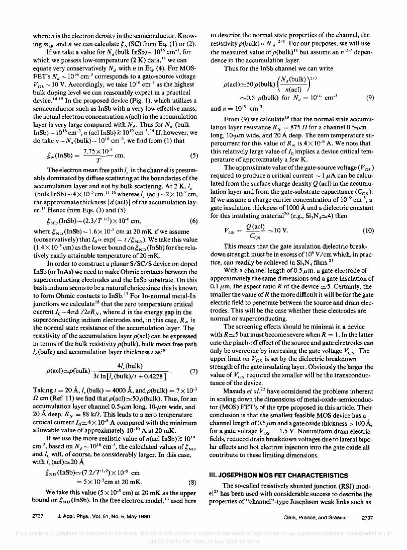
The possibility of fabricating a voltage-controlled hybrid Josephson FET junction ("JOFET") was, to our knowledge, first discussed by one of the authors I in 1971. In its simplest form the device, which is depicted in Fig. 1, consists of a coplanar superconductor-semiconductor-superconductor (source-channel-drain) Josephson junction2 with an insulated gate formed over the semiconducting channel. The function of the gate electrode, when positively biased, is to induce an accumulation layer in the surface region of the ntype semiconducting channel. We will refer to this device as a Metal-Oxide-Semiconductor (MOS) JOFET. When first considered, I heavily doped GaAs appeared to be the natural choice for the substrate material. However, in recent years it has become apparent that the high mobility III-V semiconductors InSb and InAs offer much greater potential as substrate materials. In the last two years there has been renewed interest in this kind of device,3.4 but, as yet, field effect action has not been observed in hybrid JOFET structures.
II. THE HYBRID FIELD EFFECT DEVICE
The decay of the Cooper pair probability amplitude into a normal metal at a superconducting-normal (SN) interface was first discussed by Deutscher and De Gennes.5
-7 They
found that the pair amplitude F N (x) = <P (x) exp( - Ix 1/5 N )
for large Ix I, where x is the distance into the normal metal and 5N is the pair "coherence" or decay length in this material. For a "clean" normal metal with a critical temperature (TCN) taken equal to zero,
5N = fzVFN /21TkBT, (1)
where VFN is the Fermi velocity in the normal metal. If
TCN >0,
5N ~fzVFN/21TkB T(1 - T /TCN)I/2 . (2)
In this analysis. as T -0, F N (x) decays not exponentially but much more slowly as F(x) = constant. [l!(x + xo)] For a "dirty" normal metal the effective coherence length is
(3)
where Ie is electronic mean free path. Superconductor-normal metal-superconductor (SNS)
proximity effect Josephson junctions have been fabricated successfully in both layered8 and coplanar form. 9 Similarly, coplanar superconductor-semiconductor-superconductor (S/SC/S) junctions have been prepared. 2 For the case of
SNS junctions with a thickness t of normal material, the critical current fo ex exp( - t/5 N ). For the junction to exhibit Josephson properties we require that it is phase-locked against thermodynamic fluctuations, i.e., (fz/2e) fo> kB T. Here, (fz/2e) fo is the maximum phase-coherent coupling energy of the junction. 10 It has been found experimentally for SNS junctions8 that this condition sets tmax ~85N at 4 K.
The coplanar S/SC/S MOS-JOFET device is shown in Fig. 1. Here, the accumulation layer (channel) conductance, and hence the critical current fo, can be controlled by means ofvoItage applied to the insulated gate electrode positioned above the channel. For what are considered reasonable doping levels ( :S 1016 cm-3
) the channel material should be an ntype III-V semiconductor since it appears that only this combination is suitable for low-temperature operations. II Unless very heavily doped, p-type systems always exhibit carrier freeze-out at low temperatures due to the finite ionization energy of acceptors.
In order to avoid majority carrier freeze-out while at the same time maintaining the condition (fz/2e) fo > kB T, the donor ionization energy Ed must be < kB T. Of the materials available, InSb and InAs appear to be best in this respect, followed by GaAs and InP. Thus for InSb (or InAs), Ed =Oandmeffective = 0.012 me ,II.12 where me is the free electron mass. This small value of meff ensures that the impurity band overlaps the conduction band, even at low donor concentrations (Nd ~ 1014 cm-3
). With overlap into the conduction band of the semiconductor, even at T~few K, we can use the free electron model l3 to calculate the Fermi velocity in the semiconductor VF(SC), In this approximation
vF(SC) = fz/meff(3~n)I/3 • (4)
+
aluminium gate electrode ~
source~
/ superconductlng electrodes
(indium)
gate II1sulation
/drOIll
FIG. I. Basic metal-oxide-semiconductor (MOS) JOFET configuration with Ohmic indium contacts to the source and drain; insulation 1000 A Si02
or Si,N •.
2736 J. Appl. Phys. 51(5). May 1980 0021-8979/80/052736-08$01.10 © 1980 American Institute of Physics 2736
[This article is copyrighted as indicated in the article. Reuse of AIP content is subject to the terms at: http://scitation.aip.org/termsconditions. Downloaded to ] IP:
144.32.240.51 On: Wed, 26 Nov 2014 13:38:46
where n is the electron density in the semiconductor. Knowing meff and n we can calculate SN(SC) from Eq. (1) or (2).
If we take a value for Nd(bulk InSb)-1016 cm-3, for which we possess low-temperature (2 K) data, II we can equate very conservatively Nd with n in Eq. (4). For MOSFET's Nd _1016 cm-3 corresponds to a gate-source voltage VGS -10 V. Accordingly, we take 1016 cm-3 as the highest bulk doping level we can reasonably expect in a practical device. 14.15 In the proposed device (Fig. 1), which utilizes a semiconductor such as InSb with a very low effective mass, the actual electron concentration n(acl) in the accumulation layer is very large compared with Nd. Thus for Nd (bulk InSb)-10 16 cm-3, n (acl InSb);::: 1019 cm-3.14 If, however, we do take n -Nd (bulk)-1016 cm-3, we find from (1) that
SN(lnSb)= 7.7SX1O-5
cm. (S) T
The electron mean free path Ie in the channel is presumably dominated by diffuse scattering at the boundaries of the accumulation layer and not by bulk scattering. At 2 K, le_ (bulk InSb)-4 X 10⁻⁵ cm. II .16 whereas Ie (acl)-2 X 10⁻⁷ cm, the approximate thickness {d (acl) J of the accumulation layer. 11 Hence from Eqs. (3) and (S)
SNo(lnSb)-(2.3/T 1/2) X 10-6 cm, (6)
where S NO (InSb) - 1. 6 X 10⁻⁵ cm at 20 mK if we assume (conservatively) that 10 ex: exp( - t /SNO)' We take this value (1.4 X 10⁻⁵ cm) as the lower bound onSNO (InSb) for the relatively easily attainable temperature of 20 mK.
In order to construct a planar S/SC/S device on doped InSb (or InAs) we need to make Ohmic contacts between the superconducting electrodes and the InSb substrate. On this basis indium seems to be a natural choice since this is known to form Ohmic contacts to InSb. 17 For In-normal metal-In junctions we calculate l8 that the zero temperature critical current 10-411".:1 /2eRN' where.:1 is the energy gap in the superconducting indium electrodes and, in this case, R N is the normal state resistance of the accumulation layer. The resistivity of the accumulation layer p(acl) can be expressed in terms of the bulk resistivity p(bulk), bulk mean free path I. (bulk) and accumulation layer thickness t as l9
4Ie(bulk) p(acl} .... ·p(bulk) (7)
3t In [Ie (bulk)/t + 0.4228 ]
Taking t = 20 A, Ie (bulk) = 4000 A, and p(bulk) = 7 X 10⁻³
n cm (Ref. 11) we find that p(acl)~SO p(bulk). Thus, for an accumulation layer channel O.S-,um long, 1O-,um wide, and 20 A deep, RN = 88 kil. This leads to a zero temperature critical current 10~4 X 10⁻⁸ A compared with the minimum allowable value of approximately 10-10 A at 20 mK.
If we use the more realistic value of n(acl InSb);::: 1019
cm-3, based on Nd _1016 cm-3, the calculated values of SNO and 10 will, of course, be considerably larger. In this case, with Ie (acl)~20 A
5No(lnSb)~(7.2/TI/2)X 10-6 cm
= S X 1O-5cm at 20 mK. (8)
We take this value (S X 10-5 cm) at 20 mK as the upper bound on 5No (InSb). In the free electron model, 13 used here
2737 J_ AppL Phys_, Vol. 51, No.5, May 1980
to describe the normal state properties of the channel, the resistivity p(bulk) ex: N d- 213. For our purposes, we will use
the measured value of p(bulk) I I but assume an n-2/3 dependence in the accumulation layer.
Thus for the InSb channel we can write
(NAbUlk»)2/3
p(acl)~SO p(bulk) n(acl)
~O.S p(bulk) for Nd = 1016 cm-3 (9)
and n = 10 19 cm-3•
From (9) we calculate 19 that the normal state accumulation layer resistance RN = 87S n for a channel O.S-,um long, 1O-,um wide, and 20·A deep. The zero temperature supercurrent for this value of RN is 4 X 10⁻⁶ A. We note that this relatively large value of 10 implies a device critical temperature of approximately a few K.
The approximate value of the gate-source voltage (V GS )
required to produce a critical current - 1 f..lA can be calculated from the surface charge density Q (acl) in the accumulation layer and from the gate-substrate capacitance (CGs )'
Ifwe assume a charge carrier concentration of 1019 cm-3, a gate insulation thickness of 1000 A and a dielectric constant for this insulating materiafo (e.g., Si3N4~4) then
VGS
= Q(acl) ~1O V. (10) CGS
This means that the gate insulation dielectric breakdown strength must be in excess of 106 V /cm which, in practice, can readily be achieved in Si3N4 films?1
With a channel length ofO.S f..lm, a gate electrode of approximately the same dimensions and a gate insulation of 0.1 f..lm, the aspect ratio R of the device ~S. Certainly, the smaller the value of R the more difficult it will be for the gate electric field to penetrate between the source and drain electrodes. This will be the case whether these electrodes are normal or superconducting.
The screening effects should be minimal in a device with R ~S but must become severe when R = 1. In the latter case the pinch -off effect of the source and gate electrodes can only be overcome by increasing the gate voltage V GS' The upper limit on VGS is set by the dielectric breakdown strength of the gate insulating layer. Obviously the larger the value of V GS required the smaller will be the transconductance of the device.
Masuda et al. 22 have considered the problems inherent in scaling down the dimensions of metal-oxide-semiconductor (MOS) FET's of the type proposed in this article. Their conclusion is that the smallest feasible MOS device has a channellength oro.S f..lm and a gate oxide thickness > 100 A, for a gate voltage VGS = 1.S V. Nonuniform drain electric fields, reduced drain breakdown voltages due to lateral bipolar effects and hot electron injection into the gate oxide all contribute to these limiting dimensions.
III. JOSEPHSON MOS FET CHARACTERISTICS
The so-called resistively shunted junction (RSJ) modef3 has been used with considerable success to describe the properties of "channel" -type Josephson weak links such as
Clark, Prance, and Grassie 2737
[This article is copyrighted as indicated in the article. Reuse of AIP content is subject to the terms at: http://scitation.aip.org/termsconditions. Downloaded to ] IP:
144.32.240.51 On: Wed, 26 Nov 2014 13:38:46
+
aluminium gate elect rode
source ~ ~~~'77":67777"77> gate insu!aton
/drall
semiconductor substrate (InSb or InAs) -~ ----/------'\--.-/
superconductlng electnodes (indium)
n type epitaxial layer
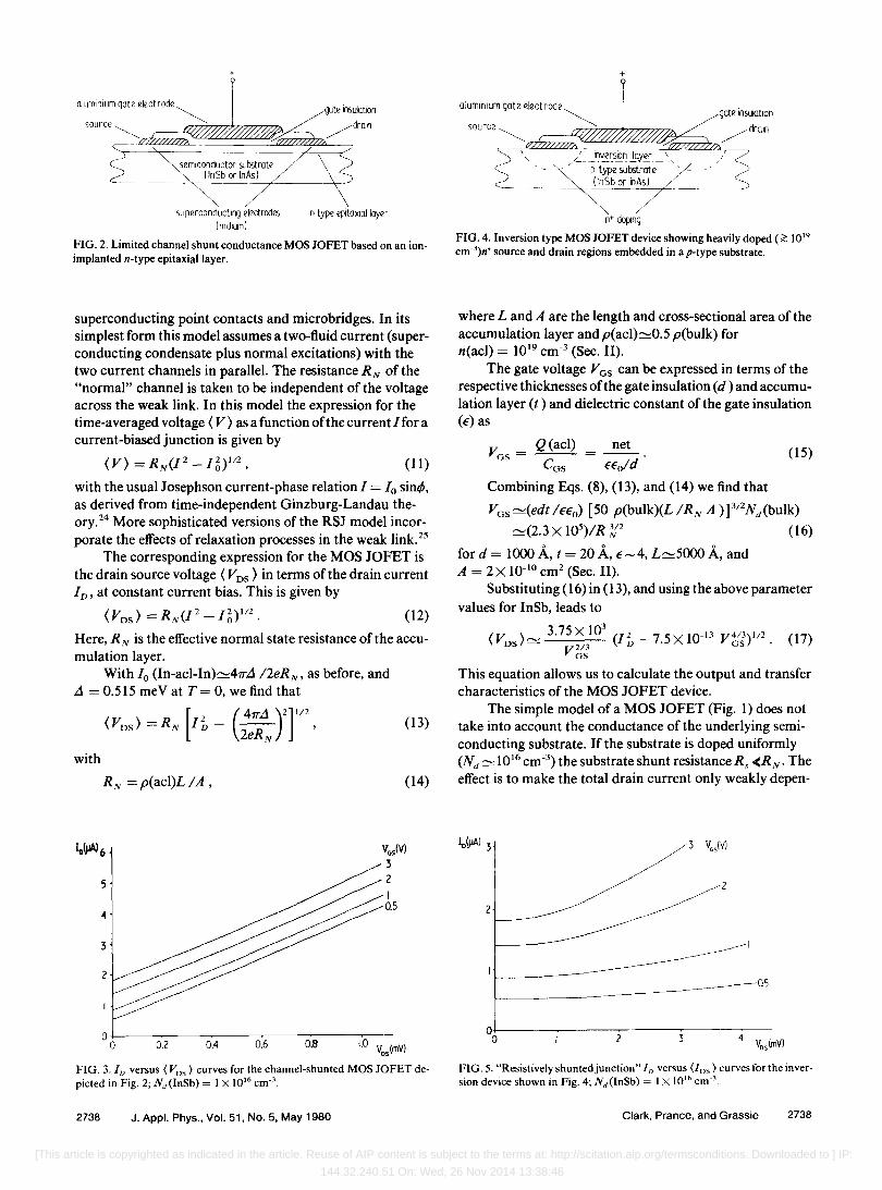
FIG. 2. Limited channel shunt conductance MOS JOFET based on an ionimplanted n-type epitaxial layer.
superconducting point contacts and microbridges. In its simplest form this model assumes a two-fluid current (superconducting condensate plus normal excitations) with the two current channels in parallel. The resistance R N of the "normal" channel is taken to be independent of the voltage across the weak link. In this model the expression for the time-averaged voltage ( V) as a function of the current I for a current-biased junction is given by
(V) = RN(/2 - 16)1/2, (11)
with the usual Josephson current-phase relation I = 10 sinc/l, as derived from time-independent Ginzburg-Landau theory.24 More sophisticated versions of the RSJ model incorporate the effects of relaxation processes in the weak link.25
The corresponding expression for the MOS JOFET is the drain source voltage ( Vos ) in terms of the drain current I D' at constant current bias. This is given by
(Vos) =RN(/2 _/6)1/2. (12)
Here, RN is the effective normal state resistance of the accumulation layer.
With 10 (In-acl-In).-....-41T..:::1 12eR N , as before, and ..:::1 = 0.515 meV at T= 0, we find that
( Vos) = R N [I ~ - C:~..:::1N r r2
,
with
RN =p(acl)LIA,
(13)
(14)
i"ljJAl6 V.5(V)
3
5 2 I 0.5 ..
3
2
O+-----~--~----~----~----~---o 0.2 0.4 0.6 0.8 1.0 V. (mV)
os
FIG. 3. In versus (VDS ) curves for the channel-shunted MOS JOFET depicted in Fig. 2; NAInSb) = 1 X 10'6 cm-'.
2738 J. Appl. Phys., Vol. 51, No.5, May 1980
+
aluminium gate electrode
source ~ ~/77.,..n777-h-r~~~ \ / -inversion layer \
~ -~/ -- P ~type~ubStrOt~- -'/ ~ __ _ (In5b or hAsI / -7
n+ doping
gate Insulation
/drOin
FIG. 4. Inversion type MOS JOFET device showing heavily doped (~ 10'9 cm-')n' source and drain regions embedded in a p-type substrate.
where L and A are the length and cross-sectional area of the accumulation layer and p(acl).-....-0.5 p(bulk) for n(acl) = 1019 cm-3 (Sec. II).
The gate voltage V GS can be expressed in terms of the respective thicknesses ofthe gate insulation (d) and accumulation layer (t) and dielectric constant of the gate insulation (€) as
VGS
= Q(acl) = ~. (15) eGS unld
Combining Eqs. (8), (13), and (14) we find that
VGS '-""-(edt luo) [50 p(bulk)(L IRN A) ]3i2NAbulk)
=(2.3 X 10⁵)IR ~2 (16)
for d = 1000 A, t = 20 A, €-4, L.-....-5000 A, and A = 2 X 10⁻¹⁰ cm2 (Sec. II).
Substituting (16) in (13), and using the above parameter values for InSb, leads to
( V, )~ 3.75x10³
(/2 -75xlO-13 V4/3)1/2 (17) os - V2/3 D' GS·
GS
This equation allows us to calculate the output and transfer characteristics of the MOS JOFET device.
The simple model ofa MOS JOFET (Fig. 1) does not take into account the conductance of the underlying semiconducting substrate. If the substrate is doped uniformly (Nd = 1016 cm-3
) the substrate shunt resistance R, <.R N • The effect is to make the total drain current only weakly depen-
lo!JJA) 3 3 VGs(V)
/2
2
L----------- 0.5
2
FIG. 5. "Resistively shunted junction" In versus (Ins) curves for the inversion device shown in Fig. 4; NAInSb) = I X 10'0 cm-~'.
Clark, Prance, and Grassie 2738
[This article is copyrighted as indicated in the article. Reuse of AIP content is subject to the terms at: http://scitation.aip.org/termsconditions. Downloaded to ] IP:
144.32.240.51 On: Wed, 26 Nov 2014 13:38:46
dent on Vos . The substrate conductance can be reduced substantially by limiting the thickness of the n-doped layer. Using ion implantation techniques this layer can be as thin as 500 ;""26 (See Fig. 2.) For this thickness, with Nd = 1016
cm-3, Rs = 300 fl for a length of 0.5 j.Lm and width 10 j.Lm. In Fig. 3 we plot (V DS ) versus I D curves at various
values of Vos for the parallel combination RN = 875 fl (9) and Rs = 300 fl. The transconductance (dID/dVOS )v,,, of the device is approximately 0.3 ,umho. From this analysis it appears that most of the current in an enhancement MOS JOFET flows through the n-type substrate and not in the weakly superconducting accumulation layer. Obviously, in an ideal device R s = 00 and the ( V DS) - I D characteristics revert to the RSJ form, as given by Eq. (17).
The substrate conductance can be eliminated by transforming the MOS JOFET into an inversion layer device,27 operating in the induced channel, enhancement mode and shown in Fig. 4. This consists of two heavily doped n-type (n+) regions a few ,um's deep which act as the source and drain. Ohmic In contacts are made to both, as in the previous device. The substrate material is lightly doped, p-type InSb. At low temperatures (less than a few K) the majority carriers in the substrate are frozen out. II However, the In/n+ regions provide sources of minority carriers (electrons) for the substrate. 28 With the In contacts superconducting, pairs and quasiparticles (normal electrons) diffuse into the substrate. The pairs break up into quasiparticles within a characteristic decay length Eq. (3). For small positive values of Vos no continuous n-type channel exists between the source and drain electrode. Since the p-type substrate is frozen out the conductance of the device is essentially zero. When Vos exceeds a critical turn-on voltage quasiparticle electrons move towards the surface of the InSb to compensate for the charge on the gate electrode. An inversion layer is thus formed and a conducting n-type channel is opened up between the source and drain.
According to Keyes 14 and Stern29 MOS FET inversion and accumulation layers are of comparable thickness for the same bulk doping level. We assume this to be approximately 20 A, as before. Figure 5 shows the I D versus Vos characteristics of the inversion layer MOS JOFET device for various values of Vos, as calculated from Eq. (17). The transconductance is approximately 1 ,umho which, since Rs = 00, cannot be increased further without changing either the dimensions of the device or the doping level, N d •
source~
_ / Shottky gate electrode
/dram
substrate (ln5b or InAs)
n type epilayer
buffer layer (hg1 purity)
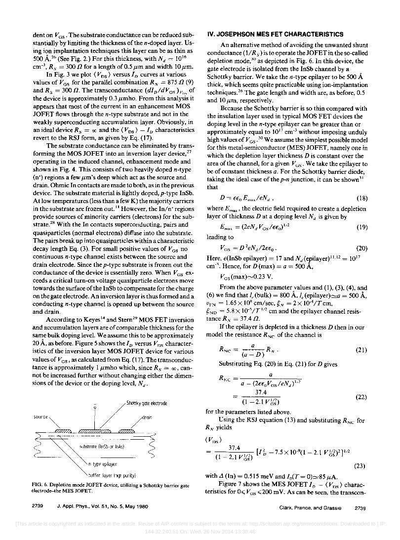
FIG. 6. Depletion mode JOFET device, utilizing a Schottky barrier gate electrode-the MES JOFET.
2739 J. Appl. Phys., Vol. 51, No.5, May 1980
IV. JOSEPHSON MES FET CHARACTERISTICS
An alternative method of avoiding the unwanted shunt conductance (1/ Rs) is to operate the JOFET in the so-called depletion mode,30 as depicted in Fig. 6. In this device, the gate electrode is isolated from the InSb channel by a Schottky barrier. We take the n-type epilayer to be 500 A thick, which seems quite practicable using ion-implantation techniques. z6 The gate length and width are, as before, 0.5 and 10 ,um, respectively.
Because the Schottky barrier is so thin compared with the insulation layer used in typical MOS FET devices the doping level in the n-type epilayer can be greater than or approximately equal to 1017 cm-3 without imposing unduly high values of Vos .30 We assume the simplest possible model for this metal-semiconductor (MES) JOFET, namely one in which the depletion layer thickness D is constant over the area of the channel, for a given Vos. We take the epilayer to be of constant thickness a. For the Schottky barrier diode, taking the ideal case of the p-n junction, it can be shown31
that
(18)
where E max ' the electric field required to create a depletion layer of thickness D at a doping level Nd is given by
Emax = (2eNd Vos/UO) liZ
leading to
(19)
Vos = D zeNd/2uo . (20)
Here, €(lnSb epilayer) = 17 and NAepilayer)".1Z = 1017
cm-3• Hence, for D (max) = a = 500 A, Vos (max)~0.23 V.
From the above parameter values and (1), (3), (4), and (6) we find that Ie (bulk) = 800 A, Ie (epilayer)=a = 500 A, VFN = 1.65 X lOR em/sec, 5N = 2 X lO-4/Tcm, 5NO = 5.8 X 1O-5/T 1/2 em and the epilayer channel resistance RN = 37.4 fl.
If the epilayer is depleted in a thickness D then in our model the resistance RNC of the channel is
a RNC = R N •
(a -D) (21)
Substituting Eq. (20) in Eq. (21) for D gives
(I - 2.1 V 2(i) (22)
for the parameters listed above. Using the RSJ equation (13) and substituting RNC for
RN yields
__ 3_7_.4 __ [It -7.5X 10⁻⁹(1-2.1 V2(i)2]1/2 (1 -2.1 V2(i)
with..::1 (In) = 0.515 meV and Io(T = 0}:::,~85 ,uA.
(23)
Figure 7 shows the MES JOFET I D - (V os) characteristics for 0.;;; Vos .;;;200 mY. As can be seen, the transcon-
Clark, Prance, and Grassie 2739
[This article is copyrighted as indicated in the article. Reuse of AIP content is subject to the terms at: http://scitation.aip.org/termsconditions. Downloaded to ] IP:
144.32.240.51 On: Wed, 26 Nov 2014 13:38:46
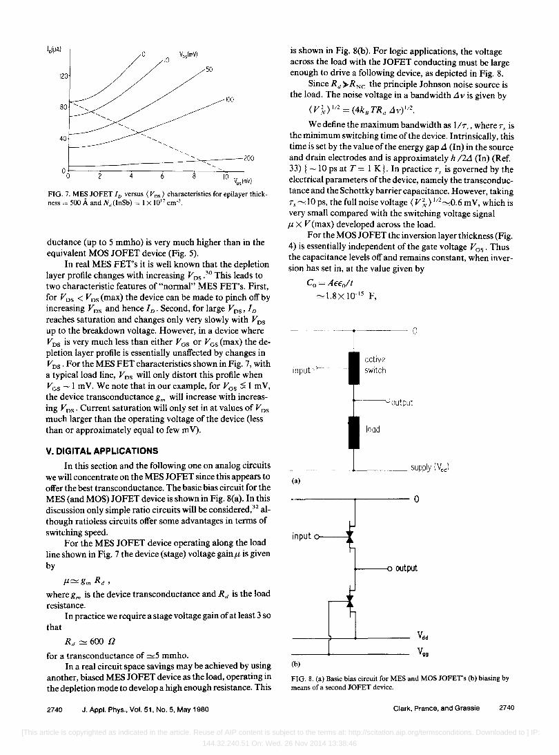
o 10
50 120
100
40
10 VoslmVJ
FIG. 7. MES JOFET 10 versus (VDS ) characteristics for epilayer thickness = 500 A and NAInSb) = 1 X 10 '7 cm-3
ductance (Up to 5 mmho) is very much higher than in the equivalent MOS JOFET device (Fig. 5).
In real MES FET's it is well known that the depletion layer profile changes with increasing Vos. 30 This leads to two characteristic features of "normal" MES FET's. First, for Vos < Vos (max) the device can be made to pinch off by increasing Vos and hence I D' Second, for large Vos, I D
reaches saturation and changes only very slowly with Vos up to the breakdown voltage. However, in a device where Vos is very much less than either Vas or Vas (max) the depletion layer profile is essentially unaffected by changes in Vos' For the MES FETcharacteristicsshown in Fig. 7, with a typical load line, Vos will only distort this profile when Vas -1 mY. We note that in our example, for Vas:;; 1 mY, the device transconductance gm will increase with increasing Vos. Current saturation will only set in at values of Vos much larger than the operating voltage of the device (less than or approximately equal to few m V).
V. DIGITAL APPLICATIONS
In this section and the following one on analog circuits we will concentrate on the MES JOFET since this appears to offer the best transconductance. The basic bias circuit for the MES (and MOS) JOFET device is shown in Fig. 8(a). In this discussion only simple ratio circuits will be considered,32 although ratioless circuits offer some advantages in terms of switching speed.
For the MES JOFET device operating along the load line shown in Fig. 7 the device (stage) voltage gain,u is given by
,u"" gm Rd ,
where g m is the device transconductance and R d is the load resistance.
In practice we require a stage voltage gain of at least 3 so that
R d "" 600 fl
for a transconductance of =5 mmho. In a real circuit space savings may be achieved by using
another, biased MES JOFET device as the load, operating in the depletion mode to develop a high enough resistance. This
2740 J. Appl. Phys., Vol. 51, No.5, May 1980
is shown in Fig. 8(b). For logic applications, the voltage across the load with the JOFET conducting must be large enough to drive a following device, as depicted in Fig. 8.
Since Rd >RNC the principle Johnson noise source is the load. The noise voltage in a bandwidth.1v is given by
(V~) 1/2 = (4kB TRd .1V)1/2.
We define the maximum bandwidth as 1 h ... where 1"s is the minimum switching time of the device. Intrinsically, this time is set by the value of the energy gap.1 (In) in the source and drain electrodes and is approximately h /2.1 (In) (Ref. 33) ! -10 ps at T = 1 K J. In practice 1"s is governed by the electrical parameters of the device, namely the transconductance and the Schottky barrier capacitance. However, taking 1", = 10 ps, the full noise voltage (V~) 1/2=0.6 m V, which is very small compared with the switching voltage signal ,u X V (max) developed across the load.
For the MOS JOFET the inversion layer thickness (Fig. 4) is essentially independent of the gate voltage Vas. Thus the capacitance levels off and remains constant, when inversion has set in, at the value given by
Co =AEEoIt
= 1.8 X 10⁻¹⁵ F,
input
(a)
actiw switch
load
o
output
----------~-------o
input 0---'-1' ~~
(b)
t-----"o output
FIG. 8. (a) Basic bias circuit for MES and MOS JOFET's (b) biasing by means of a second JOFET device.
Clark, Prance, and Grassie 2740
[This article is copyrighted as indicated in the article. Reuse of AIP content is subject to the terms at: http://scitation.aip.org/termsconditions. Downloaded to ] IP:
144.32.240.51 On: Wed, 26 Nov 2014 13:38:46
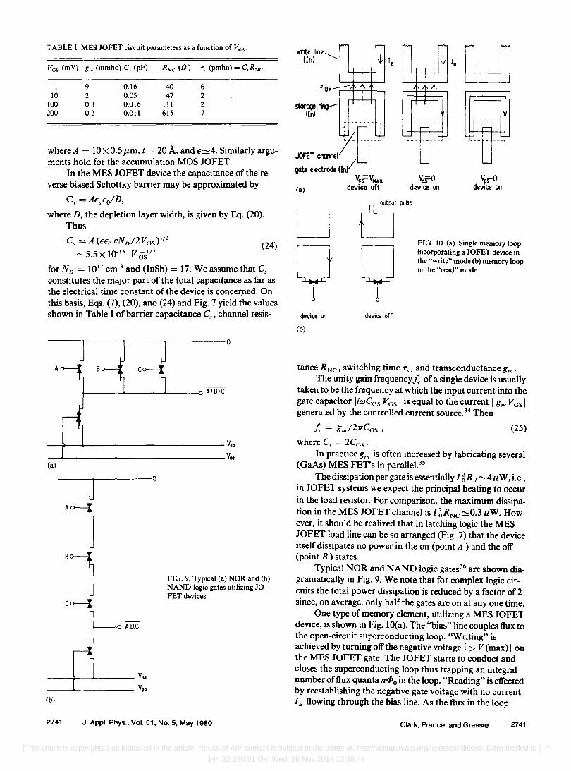
TABLE I. MES JOFET circuit parameters as a function of VGs.
Vos (mV) gm (mmho) C, (pF) RNc (11) T, (pmho) = C,RNC
I 10
100 200
9 2 0.3 0.2
0.16 0.05 0.016 O.otl
40 47
III 615
6 2 2 7
whereA = IOXO.5 j.tm, t = 20 A, and E::::::::4. Similarly arguments hold for the accumulation MOS JOFET.
In the MES JOFET device the capacitance of the reverse biased Schottky barrier may be approximated by
C, =AEsEoID,
where D, the depletion layer width, is given by Eq. (20). Thus
Cs =A(uoeNDI2VGs)I/2 (24) ::::::::5.5 X 10⁻¹⁵ V OSI12
for ND = 1017 cm-3 and (InSb) = 17. We assume that Cs
constitutes the major part of the total capacitance as far as the electrical time constant of the device is concemed. On this basis, Eqs. (7), (20), and (24) and Fig. 7 yield the values shown in Table I of barrier capacitance Cs ' channel resis-
------r------,------r----------o
A
~------L-------L-----~A+B+C
--~--~--------------------------~. --~------------------------------~. (a)
------~---------O
A
B
-----t---+------- Vd•
____ ~ ___________ V ••
(b)
FIG. 9. Typical (a) NOR and (b) NAND logic gates utilizing JOFET devices.
2741 J. Appl. Phys., Vol. 51, No.5, May 1980
write line '--... (In)
flux
stora;Jl! rrg(In)
r - - - - - - 1 T _. --~ '0 ' ..oFET chcmel
gate electrode Unl
(a)
device al
(b)
VGrVNAX device off
device off
'"7 ______ ~
Vci=0 device on
~ __ - __ :T
Vci=0 device on
FIG. 10. (a). Single memory loop incorporating a JOFET device in the "write" mode (b) memory loop in the "read" mode.
tance R NC ' switching time 7 s, and transconductance gm. The unity gain frequency fc of a single device is usually
taken to be the frequency at which the input current into the gate capacitor liwCGS VGS I is equal to the current I gm VGS I generated by the controlled current source. 34 Then
fc = gm I21TCGS , (25)
where Cs = 2CGS •
In practice gm is often increased by fabricating several (GaAs) MES FET's in paralle1.35
The dissipation per gate is essentially nRd ::::::::4j.tW, i.e., in JOFET systems we expect the principal heating to occur in the load resistor. For comparison, the maximum dissipation in the MES JOFET channel is I~RNc ::::::::0.3 j.tW. However, it should be realized that in latching logic the MES JOFET load line can be so arranged (Fig. 7) that the device itself dissipates no power in the on (point A ) and the off (point B) states.
Typical NOR and NAND logic gates36 are shown diagramatically in Fig. 9. We note that for complex logic circuits the total power dissipation is reduced by a factor of 2 since, on average, only half the gates are on at anyone time.
One type of memory element, utilizing aMES JOFET device, is shown in Fig. lO(a). The "bias" line couples flux to the open-circuit superconducting loop. "Writing" is achieved by turning off the negative voltage I > V (max) J on the MES JOFET gate. The JOFET starts to conduct and closes the superconducting loop thus trapping an integral number offtux quanta n<Po in the loop. "Reading" is effected by reestablishing the negative gate voltage with no current I B flowing through the bias line. As the flux in the loop
Clark, Prance, and Grassie 2741
[This article is copyrighted as indicated in the article. Reuse of AIP content is subject to the terms at: http://scitation.aip.org/termsconditions. Downloaded to ] IP:
144.32.240.51 On: Wed, 26 Nov 2014 13:38:46
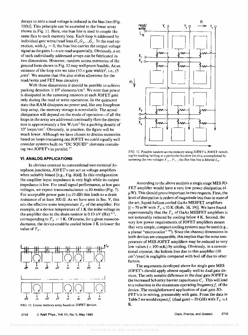
decays to zero a read voltage is induced in the bias line (Fig. lO(b)]. This principle can be extended to the linear array shown in Fig. 11. Here, one bias line is used to couple the same flux to each memory loop. Each loop is addressed by individual gate write/read lines G"G2 , •.. ,Gn • In the read operation, with I B = 0, the bias line carries the output voltage signal as the gates l···n are read sequentially. Obviously, a set of such individually addressed arrays can be fabricated in two dimensions. However, random access memories of the general form shown in Fig. 12 may well prove feasible. As an estimate of the loop size we take (lOx gate width)2, i.e., (5 ,um)2. We assume that this also makes allowance for the read/write and FET bias circuitry.
With these dimensions it should be possible to achieve packing densities ;(; 106 elements/cm2. We note that power is dissipated in the summing resistors at each JOFET gate only during the read or write operations. In the quiescent state this RAM dissipates no power and, like any Josephson loop array, the memory storage is nonvolatile. The actual dissipation will depend on the mode of operation-if all the loops in the array are addressed continually then the dissipation is approximately a few W /cm2 for a packing density of 106 100ps/cm2
• Obviously, in practice, the figure will be much lower. Although we have chosen to discuss memories based on loops containing one JOFET we could equally well consider systems built on "DC SQUID" elements containing two JOFET's in parallel. 37
VI. ANALOG APPLICATIONS
In obvious contrast to conventional two-terminal Josephson junctions, JOFET's can act as voltage amplifiers when suitably biased [e.g., Fig. 8(a)]. In this configuration the amplifier input impedance is very high while its output impedance is low. For small signal performance, at low gate voltages, we expect transconductance '"" 10 mmho (Fig. 7). For acceptable power gain (c:::dO dB) this leads to a drain resistance of at least 300 n. As we have seen in Sec. V, this sets the effective noise temperature TN of the amplifier. For example, at a device temperature of 1 K the noise voltage in the amplifier due to the drain resistor is 0.13 n V (Hzt'/2, corresponding to T", = 1 K. Of course, for a given transconductance, the device could be cooled below 1 K to lower the value of T,\'.
i 1111~111111111~1~11I11~1" TTTTTTTT ~ 00 ~ ~ 00 00 ~ 00
I 101 I Inlo1 101 TTTTTTTT ~ 00 ~ ~ 00 00 ~ 00
FIG. 11. Linear memory array based on JOFET devices.
2742 J. Appl. Phys., Vol. 51, No.5, May 1980
Y, read/ write LBV-------7-----~------~
X, o---~~--?_--~--~--~ X2 o---~~--?_--,_--~--~
FIG. 12. Possible random access memory using JOFET's; JOFET switching for reading/writing at a particular location (m,n) is accomplished by summing the two voltages V""' V,,, ; the flux bias line is labeled Ln.
According to the above analysis a single stage MES JOFET amplifier would have a very low power dissipation (4 ,u W). This should prove important in two respects. First, the level of dissipation is orders of magnitude less than in state of the art, liquid-helium cooled GaAs MESFET amplifiers [( -70 mW with T:'V.:;;; 10 K (Refs. 38, 39)]. We have found experimentally that the TN of GaAs MESFET amplifiers is not noticeably reduced by cooling below 4 K. Second, the very low power requirements of JOFET amplifiers means that very simple, compact cooling systems may be used (e.g., a planar "microcooler" 40). Since the channel dimensions in both devices are comparable, this implies that the noise temperature of MES JOFET amplifiers may be reduced to very low values ( < 100 mK) by cooling. Obviously, in a conventional cryostat, the helium loss due to this amplifier (10 cm3/year) is negligible compared with boil off due to other factors.
The arguments developed above for single gate MES JOFET's should apply almost equally well to dual gate devices. The only notable difference in the dual gate JOFET is the increased Schottky barrier capacitance Cs • This wi1l1ead to a reduction in the maximum operating frequency fc of the device. The straightforward application of dual gate JOFET's is in mixing, presumably with gain. From the data in Table I we would expectfc ( dual gate) - 20 G Hz with TN c:::; 1 K.
Clark, Prance, and Grassie 2742
[This article is copyrighted as indicated in the article. Reuse of AIP content is subject to the terms at: http://scitation.aip.org/termsconditions. Downloaded to ] IP:
144.32.240.51 On: Wed, 26 Nov 2014 13:38:46
VII. SUMMARY AND CONCLUSIONS
We have calculated the effective coherence or decay length ~ND for Cooper pairs along a channel of doped InSb in a proposed Josephson Field Effect (JOFET) device. We show that for the worst and best cases ~ ND at 20 mK can vary between approximately 0.5 J-lm and a few J-lm, depending on the form of the device (MOSFET or MESFET). With a channel length of 0.5 J-lm, well within the current state of the lithographic art, we estimate the range of zero temperature critical currents to be between a few J-lA and 100 J-lA. This implies device critical temperatures - few K.
Our calculations suggest that the search for FET action in JOFET devices with relatively long channels (-0.5 J-lm) should be undertaken at low temperatures, certainly < 100 mK, in order to maximize the value of ~ND' This has not yet been attempted. We must also expect early devices to display less than optimum performance, e.g., through poor channel definition, poor Ohmic contact between source and drain electrodes and the semiconductor substrate, etc. This further strengthens the case for very low temperature measurements.
The estimates of JOFET performance made in this paper are based on the still limited data available on the properties of small band gap materials ~uch as InSb. 11.12 Even so, predicted switching speeds and power dissipation appear to be comparable with the best available conventional Josephson devices. 37 We must assume that a more judicial choice of device parameters such as doping level, channel length, channel thickness and superconducting source and drain material will lead to improved performance, particularly with regard to the temperature of operation. We also assume that the choice of channel material will not be limited to InSh-any small band gap semiconducting material with high carrier mobility and essentially zero carrier ionization energy will suffice. 12
'T.D. Clark, Ph.D. Thesis, University of London, 1971 (unpublished). 'M. Schyfter, J. Maah-Sango, N. Raley, R. Ruby, RT. Ulrich, and T. van Duzer, Proc. Appl. Superconductivity Conf., Stanford, California, August, 1976 (unpublished).
'A. Silver, A Chase, M. McColl, and M. Millea, Conference on Future Trends in Superconductive Electronics, Charlottsville, Va., March 1978 ( unpublished).
"M.F. Millea, A.H. Silver, and L.D. Fiesner, Appl. Superconductivity Conf., Pittsburg, Pa., Sept. 1978 (unpublished).
'G. Deutscher and P.G. de Gennes, Proximity Effects in Superconductivity, edited by R.D. Parks (Marcell Dekker, New York, 1969), p. 1005.
'H.J. Fink, Phys. Rev. B 14, 1028 (1976). 7H.J. Fink and R.S. Poulsen, Phys. Rev. B 18 (1978). "J. Clarke, Proc. Int. Conf. on Low Temperature Physics (12), Kyoto, Japan, Sept. 1970. p. 443 (unpublished); Proc. Roy. Soc. A 308, 447 (1969). ~H.W. Notarys and J.E. Mercereau, J. Appl. Phys. 44, 1821 (1973); E.P. Harris, IEEE Trans. Mag. MAG-H, 785 (1975).
"'See for example, Tinkham, Introduction to Superconductivity (McGrawHill, Kogakusha, 1975), p. 212.
liB. Lengeler, Cryogenics 14, 439 (1974).
2743 J. Appl. Phys., Vol. 51, No.5, May 1980
12E.H. Putlye, Proc. Phys. Soc. 73, 280 (1959); see also Semiconductors, edited by R.A. Smith (Cambridge D.P., Cambridge, 1978), Chap. 12 and 13 for more information on small band gap (III-V) semiconductors.
I 'N. W. Ashcroft and N.D. Mermin, Solid State Physics (Holt, Rinehart and Winston, New York, 1976), p. 36.
I4R. W. Keyes, A Perspective 0/ PhYSics, edited by Sir Rudolf Peierls (Gordon and Breach, London, 1977), Vol. I, p. 81.
"See, for example, S.M. Sze, Physics o/Semiconductor Devices (Wiley, New York, 1969), Chap. 10, for a review of MOS devices.
"H.M. Rosenberg, Low Temperature Solid State Physics (Clarendon, Oxford, 1965), p. 74.
17J. Shannon, Philips Research Laboratories, Sal fords, Surrey (private communication); Sol. State Electron. 18, 541 (1975).
"P.G. De Gennes, Superconductivity 0/ Metals and Alloys (Benjamin, New York, 1966), p. 238.
'"For Fuchs-Sondheimer scattering in thin conducting films see, for example, O.S. Heavens, Thin Film Physics, (Methuen, London, 1977), p. 116.
2°E(Si,N4) depends on the methods of preparation but is typically 4 [1. Shannon, Philips Labs., Salfords, Surrey, England (private communication)].
2IS.M. Sze, Physics o/Semiconductor Devices (Wiley. New York, 1969), p. 500.
22H. Masuda, M. Nakai, and M. Kubo, IEEE Trans. Electron. Devices ED-26, 980 (\ 979).
23D.E. McCumber, J. Appl. Phys. 39, 3113 (1968); W.e. Stewart, Appl. Phys. Lett. 12, 277 (1968).
24L.G. Aslamazov and A.I. Larkin, JETP Lett. 9,87 (1969). 25See, for example, H.H. Jensen and P.E. Lindelof, J. Low Temp. Phys. 23,
469 (1976); T.D. Clark and P.E. Lindelof, Phys. Rev. Lett. 37,368 (1976). "e. Reece, Plessey Laboratories, Towcester, England (private communica
tion); see also G. Zimmer, B. Hoeffiinger, and 1. Schneider, IEEE Trans. Electron. Devices ED-26, 390 (1979), for examples of ion implantation in MOS FET devices.
27See, for example, T.H. Beeforth and H,J. Goldsmid, Physics o/Solid State Devices (Pion, London, 1970); S.M. Sze, Physics o/Semiconductors Devices (Wiley, New York, 1969), p. 429.
'"J. Shannon, Philips Laboratories, Redhill, England (private communication).
2°F. Stern, in Proc. 10th Con! on the Physics 0/ Semiconductors (National Technical Information Service, Springfield, Va., 1970), pp. 451-458.
.'°See, for example, T.H. Beeforth and H,J. Goldsmid, Physicso/Solid State Devices (Pion, London, 1970), p. 73; S.M. Sze (Wiley, New York, 1969), Chap. 10; Glaser and Subak-Sharpe, Integrated Circuit Engineering (Addison-Wesley, New York, 1978), Chap. 3.
"J.E. Carroll, Physical Models/or Semiconductor Devices (Edward Arnold, London, 1974), p. 152.
'''See, for example, J. Mavor, MOST Integrated Circuit Engineering (Peter Peregrinus, Stevenage, England, 1973), p. 46.
"See, K.K. Likharev, Rev. Mod. Phys. 51,101 (1979); J.R. Waldram, Rep. Prog. Phys. 39, 751 (1976), for reviews of the high-frequency properties of Josephson junctions.
.'4e.A. Liechti, IEEE Trans. Microwave Theory and Techniques MIT-24, 279 (1976).
"For example, Plessey GAT 6 GaAs FET's contain two parallel FET devices on one chip (Plessey Electro-optical Devices Co. Ltd., Towcester, Northamptonshire, United Kingdom).
."See, J. Mavor, MOST Integrated Circuit Engineering (Peter Peregrinus, Stevenage, England, 1973), for descriptions ofFET-based NOR and NAND circuits.
HSee, J. Matisoo, in Proc. L.T.15 Conference, Rev. de Phys. III, C6-1590, 1978 (unpublished); W. Anacker, IEEE Spectrum 16,26 (1979); D.J. Herrell, in Conf. Proc. ofInt. Cryogenics Eng. Conf., Vol. 7, July 4--8, 1978 (unpublished); for current reviews of Josephson junction computer technology.
'"A.P. Long, T.D. Clark, R.1. Prance, and M.G. Richards, Rev. Sci. Instrum. 50, 1376 (1979).
W A.P. Long, T.D. Clark, and R.J. Prance, Rev. Sci. Instrum. 51, 85 (19xx). 4<IW.A. Little, in AlP Conf. Proc. 44, 421 (1978).
Clark, Prance, and Grassie 2743
[This article is copyrighted as indicated in the article. Reuse of AIP content is subject to the terms at: http://scitation.aip.org/termsconditions. Downloaded to ] IP:
144.32.240.51 On: Wed, 26 Nov 2014 13:38:46