Embed Size (px)
Citation preview

30 IEEE CIRCUITS AND SYSTEMS MAGAZINE 1531-636X/10/$26.00©2010 IEEE SECOND QUARTER 2010
Feature
Digital Object Identifier 10.1109/MCAS.2010.936784
ESD Avoiding Circuits for Solving OTP Memory Falsely Programmed Issues
Shao-Chang Huang, Ke-Horng Chen, Hsin-Ming Chen, Ming-Chou Ho, and Rick Shih-Jye ShenAbstract
One-time program (OTP) memories are pro-grammed for memory design without elec-trostatic discharge (ESD) stresses. However, in reality, ESD events are not selective and thus ESD currents can falsely program OTP memory cells. Many integrated circuit (IC) designers focus only on improving OTP mem-ory control architectures to avoid memory being falsely programmed without mention-ing the ESD-introduced memory errors. This article investigates a new ESD architecture and novel ESD avoiding circuits, aiming to solve ESD-introduced memory falsely pro-grammed issues. It should be noted that this article focuses on ESD circuit designs to pro-tect OTP memory instead of OTP control ar-chitectures. With such new ESD schemes, our prototype circuits have demonstrated that memory cells can indeed be programmed at IC program mode without ESD stresses.
© S
TO
CK
BY
TE
& P
HO
TO
DIS
C

SECOND QUARTER 2010 IEEE CIRCUITS AND SYSTEMS MAGAZINE 31
I. Introduction
Embedded non-volatile memory devices can provide
capabilities for system program code storage, con-
figuration setting, and product identification set-
ting [1–4]. However, the complexity of device fabrication
may lead to low product yield and high process cost. In
this article, a new embedded one time programmed bit-
cell (Neobit) [5] device, fabricated by mature process
technologies with minor changes, is used as the memo-
ry cell. It is noted that such non-volatile OTP memories
should be programmed under IC program mode, but
should not be programmed under IC read and other IC
operation modes. ESD events can induce non-volatile
memories falsely programmed under IC transportations
and other unpredicted stresses. This article focuses on
the issue of how to avoid ESD falsely programming of
non-volatile memories.
In this study, Neobit is said to be programmed if Neobit
has current equal to or larger than 1 mA. If Neobit is not
operated under program processes, but the memory cell
is programmed on unpredicted occasions, the status is
referred to as the memory falsely programmed issue.
ESD device turn-on voltage (Vt1) must be designed
to be larger than the programming voltage (Vprog), so
that ESD protection devices can keep the off state dur-
ing IC program operations. On the contrary, Vt1 must be
designed as small as possible, so that ESD device can
turn on effectively to protect Neobit. Although the Neobit
programmed time (100 ms) is much larger than the ESD
event time ( , 1 ms), large Vt1 can still result in memory
falsely programmed under ESD stresses. This is because
ESD currents possibly enter Neobit if ESD device does
not turn on to dissipate ESD charges. In this article, ESD
avoiding circuit [6], which uses one inverter for control-
ling transmission N/PMOS transistors, is designed for
preventing ESD currents from entering OTP cells.
This IC test-chip is processed by 0.25 mm silicon
technology and there are four kinds of Voltage Program
PAD (VPP) circuits under the framework of this article.
The first VPP circuit, Circuit A, is Gate-Grounded NMOS
transistor (GGNMOST); the second, Circuit B, is Gate-
Driven NMOS transistors (GDNMOST); the third, Circuit
C, uses a GGNMOST as ESD protection circuit and an ESD
avoiding circuit as ESD current stopping wall between
VPP and OTP memory cells; the last, Circuit D, consists
of GDNMOST and ESD avoiding circuit.
Firstly, Circuit A cannot bypass ESD currents effectively
and cannot prevent ESD currents from entering OTP cells,
consequently OTP cells will encounter falsely memory
programmed issues. Secondly, Circuit B can obtain a
much lower Vt1, but memory falsely programmed issue
still exists because ESD currents are not selective to flow
only into ESD NMOS transistors. Thirdly, Circuit C still has
memory falsely programmed issue, where although ESD
avoiding circuit is designed for preventing ESD currents
from entering OTP cells, GGNMOST cannot effectively
dissipate ESD currents. Finally, Circuit D has no memory
falsely programmed issue because GDNMOST can turn on
effectively under ESD stresses and ESD avoiding circuit
can prevent ESD currents from entering OTP cells.
To carry out the study below, in Section II memory ar-
chitecture description is firstly described. ESD circuits
are then discussed in Section III and ESD testing experi-
ments are listed in Section IV. Finally, to analyze and
demonstrate the results, falsely programming analysis
and simulation analysis are presented in Section V and
Section VI, respectively.
II. Memory Architecture Description
Metal fuse is often used as one switch, as illustrated in
Fig. 1(a). Under IC normal operation conditions, terminal
A connects to terminal B. Once large currents flow
through the metal to burn it out, terminal A disconnects
to terminal B and there is an opening with a very high
resistor between the two terminals. However, the
Figure 1. Traditional metal fuse and OTP memory appli-cations. (a) shows the traditional metal fuse, (b) shows switch controlled under OTP memory, and (c) shows one transmission gate structure and one inverter as the switch connected with OTP memories.
A
B
A
B
Switch OTP
A
B
OTP
Switch
(c)(b)(a)
Shao-Chang Huang ([email protected]) and Ke-Horng Chen are with the Institute of Electrical and Control Engineering, National Chiao Tung
University, Hsinchu, Taiwan. Hsin-Ming Chen, Ming-Chou Ho, and Rick Shih-Jye Shen are with the eMemory Technology Inc., Hsinchu, Taiwan.
Embedded non-volatile memory devices can provide capabilities for system program code storage, configuration setting, and product identification setting.

32 IEEE CIRCUITS AND SYSTEMS MAGAZINE SECOND QUARTER 2010
opening gives an entrance for contaminants, such as
water vapor, which destroy surrounding devices, and
as a result this lowers the reliability of the surrounding
devices. Metal cut is a relatively more time-consuming
procedure since enough heats are necessary to cut the
metal. Furthermore, metal fuse cannot be connected
under electrical operations after the metal is cut.
Due to the above three major disadvantages of metal
fuse, easy contaminant entrance, time-consuming metal
cut and non-recovered characteristics under electrical
operations, one-time program memory (OTP) is applied to
replace metal fuse here. Fig. 1(b) illustrates OTP memory
which controls the switch. If OTP memory provides a
low-level voltage before it is programmed and provides
a high-level voltage after it is programmed, OTP memory
can connect terminal A and terminal B together before
OTP memory is programmed, whereas OTP memory can
disconnect terminal A and terminal B after OTP memory
is programmed. The detailed structure of OTP memory,
which controls the switch, is shown in Fig. 1(c). Herein,
terminals A and B become the switch composing of
transmission N/PMOS transistors and one inverter.
Fig. 2 illustrates the Neobit architecture [7] that forms
the OTP memory cell in this study. It contains two PMOS
transistors. The 1st PMOS transistor operates as one
switch and the 2nd PMOS transistor is the programmed
cell. When performing the program operations, word-
line voltage VSG is applied on the selected poly gate of
the 1st PMOS transistor, thereby turning on a P-channel.
A source-line voltage VSL is applied on the P1 source
region of 1st PMOS transistor and is connected to the
programming bonding VPP. A well voltage VNW is applied
on the N-well. A bit-line voltage VBL is applied on the
P1 drain region of the 2nd PMOS transistor. The floating
gate of the 2nd PMOS transistor is in a floating state.
Under the above voltage conditions, a coupling voltage
is sensed by the floating gate due to capacitive coupling
effect, thereby turning on a P-channel under the
floating gate. Hot carriers such as electrons, which are
accelerated by the electric field at the depletion region,
tunnel through the floating poly gate oxide layer by
way of the turned on P-channel, and are finally trapped
inside the P1 floating poly gate.
Fig. 3 indicates OTP cell operations [8]. On the one
hand, PMOS transistor P1 and NMOS transistor N1 turn
on at the IC program mode. VPP is connected to 7 V
so that PMOS transistor P2 can be programmed. If the
OTP cell is not designed for being programmed, both
transistors P1 and N1 will turn off. On the other hand,
P1 turns on but N1 turns off at the IC read mode. Both
PMOS transistors P3 and P4 turn on and VPP is tied to
3.3 V. If P2 is programmed, then terminal D can own a
high-level voltage so that terminal Dout can obtain a
low-level voltage. Then, data output terminal DBout
obtains a high-level voltage. On the contrary, DBout can
obtain a low-level voltage if P2 is not programmed.
Briefly summarizing, OTP memory can provide a
high-level voltage if Neobit is programmed and OTP
memory can provide a low-level voltage if Neobit is
not programmed. Through selecting Neobit to be
programmed or non-programmed, IC designers can obtain
switch-off or switch-on functions. Since Neobit operates
under electrons, absorbed in floating poly gate oxide for
being programmed, the electrons permanently exist in
the floating poly gate oxide after the cell is programmed,
except that the cell is exposed in the complicated cell
Figure 3. Neobit program and read operation circuit.
VPP
FGDLU
P2
P3
P4 P5
N1
PGM
DIN
N2 N3
Dout
RE
ZEN
BIAS
P1SL
Program
Path Read Path
D DBout
Figure 4. IC bonding pad assignment.
VDDPORVSS
PTM[1:0]
PA[1:0]PWE
PDIN[7:0]
PDOB[31:0]VPP
5 µm
5 µm
X = 137 µm Y = 50 µm
OTP Fuse
Logic Device Block
5 µm
VPP
X
Y
Figure 2. Neobit structure and operation.
P+ P+ P+
VSG VFG
VBL
VSL
(VPP)
Second PMOSFirst PMOS
N-Well

SECOND QUARTER 2010 IEEE CIRCUITS AND SYSTEMS MAGAZINE 33
recovery procedures. In other words, electrons cannot
be changed even the power supply turns off, so switch-
off and switch-on characteristics such as the metal fuse
characteristics cannot be easily changed.
There exist not only Neobit but also many other kinds
of bonding pads for providing IC suitable operation
voltages in OTP memories, as shown in Fig. 4. VDD
provides IC power supply and VSS provides IC grounding
signals. POR gives power-on reset function and PTM is
for test mode enabling. VPP is a 7 V pad in program cycle
and a 3.3 V pad in read cycle. PA is the address input for
program control and PWE defines program cycle. PDIN
is designed for data input and PDOB is designed for data
output [9]. Fig. 5 and Fig. 6 illustrate test-chip layout and
microphotograph, respectively. The IC test-chip circuits
can be classified into three major parts, OTP memory
control circuit (CTL), OTP memory cells and I/O circuits.
According to Neobit operations and other control
signals, circuit designers can obtain switch-on or switch-
off characteristics from OTP memory. OTP memory not
only owns the same switch functions as metal fuse,
but also overcomes metal fuse’s three disadvantages.
Firstly, OTP memory has no contaminant issue because
there is no metal opening. Secondly, all the OTP memory
programmed operation procedures are finished under
electrical controls, so much time is saved in OTP
memory. Finally, OTP memory users can use UV photo
to delete floating PMOS transistor poly gates’ electrons,
so they can recover IC to the pre-programmed status
under electrical operations.
Unlike other types of Flash memories, Neobit structure
is not suitable for multiple-time being pro grammed and
erased, because UV photo consumes much time for
memory erasure and charges are
stored in the poly gate oxide. Neobit
is designed for being programmed
and erased in the applications with
recycling frequencies less than 10,
although they can be used in more
cycles. This is the so-called One-
Time Program (OTP) memory.
III. ESD Circuit Discussion
In order to protect IC against ESD damage while not
to let ESD circuit interfere IC normal operations, Gate-
Grounded NMOS transistors are often used as ESD circuit,
such as Circuit A discussed above. To reduce ESD device
turn-on voltage, power-up reset circuit [10] is used to
locate the poly gate of ESD NMOS transistor for forming
Gate-Driven circuit, as illustrated in Circuit B. Although
there are ESD protection circuits, ESD currents can
enter OTP memories from VPP, so ESD avoiding circuit
is proposed to stop ESD currents. Circuit C combines
Circuit A and ESD avoiding circuit. Circuit D combines
Circuit B and ESD avoiding circuit. Circuits A-D will be
described below in more details.
For negative ESD charges, they can be easily dissipated
by the parasitic diode D1 of Circuits A-D, therefore the
descriptions given below will focus on positive ESD
charges only. Moreover, from IC area consumption
points of view, GGNMOST is much saved as compared
to GDNMOST, because ESD-driven circuits cost a lot
of layout area. Normally, the gate-driven circuit layout
size is almost equal to ESD NMOS transistor size. This
is the other reason why GGNMOST is the typical ESD
protection circuit. However, such simple ESD protection
circuit cannot protect OTP memory cells from ESD
damages, so we need to discover the new ESD circuit.
Circuit A: Gate-Grounded NMOS
Transistor (GGNMOST)
GGNMOST is often used as ESD protection device, as
illustrated in Fig. 8. There are NMOS transistor N2 as
ESD device and one gate-coupled resistor R1 between
transistor N2 poly gate and grounding terminal VSS.
Figure 5. IC test chip layout, including OTP cells, control circuits (CTL), and input/output (I/O) circuits.
VPP
I/O Circuit
OTP OTP OTP OTPCTL CTL CTL CTL
Figure 6. IC test chip microphotograph, including OTP cells, CTL, and I/O circuits.
34 IEEE CIRCUITS AND SYSTEMS MAGAZINE SECOND QUARTER 2010
Under IC normal operations, there are no leakage currents
because transistor N2 poly gate is connected to VSS
through R1. The parasitic NPN bipolar of transistor N2
can turn on to dissipate ESD currents under positive ESD
stresses [11]. When positive ESD events occur, Isub can
go through Rsub to make base-emitter voltage VBE larger
than 0.7 V and then turn on the parasitic bipolar.
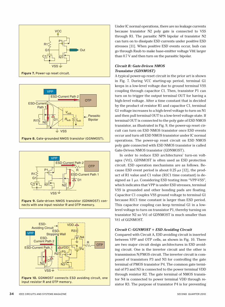
Circuit B: Gate-Driven NMOS
Transistor (GDNMOST)
A typical power-up reset circuit in the prior art is shown
in Fig. 7. During VCC starting-up period, terminal G1
keeps in a low-level voltage due to ground terminal VSS
coupling through capacitor C1. Then, transistor P1 can
turn on to trigger the output terminal OUT for having a
high-level voltage. After a time constant that is decided
by the product of resistor R1 and capacitor C1, terminal
G1 voltage increases to a high-level voltage to turn on N1
and then pull terminal OUT to a low-level voltage state. If
terminal OUT is connected to the poly gate of ESD NMOS
transistor, as illustrated in Fig. 9, the power-up reset cir-
cuit can turn on ESD NMOS transistor once ESD events
occur and turn off ESD NMOS transistor under IC normal
operations. The power-up reset circuit on ESD NMOS
poly gate connected with ESD NMOS transistor is called
Gate-Driven NMOS transistor (GDNMOST).
In order to reduce ESD architectures’ turn-on volt-
ages (Vt1), GDNMOST is often used as ESD protection
circuit. ESD operation mechanisms are as follows. Be-
cause ESD event period is about 0.25 ms [12], the prod-
uct of R1 value and C1 value (R1C1 time constant) is de-
signed as 1 ms. Considering ESD testing item “VPP-VSS”,
which indicates that VPP is under ESD stresses, terminal
VSS is grounded and other bonding pads are floating.
Capacitor C1 couples VSS ground voltage to terminal G1
because R1C1 time constant is larger than ESD period.
This capacitor coupling can keep terminal G1 in a low-
level voltage to turn on transistor P1, thereby turning on
transistor N2 so Vt1 of GDNMOST is much smaller than
Vt1 of GGNMOST.
Circuit C: GGNMOST 1 ESD Avoiding Circuit
Compared with Circuit A, ESD avoiding circuit is inserted
between VPP and OTP cells, as shown in Fig. 10. There
are two major circuit design architectures in ESD avoid-
ing circuit. One is the inverter circuit and the other is
transmission N/PMOS circuit. The inverter circuit is com-
posed of transistors P3 and N3 for controlling the gate
terminal of PMOS transistor P4. The common gate termi-
nal of P3 and N3 is connected to the power terminal VDD
through resistor R2. The gate terminal of NMOS transis-
tor N4 is connected to power terminal VDD through re-
sistor R3. The purpose of transistor P4 is for preventing
Figure 7. Power-up reset circuit.
G1
C1
R1P1
N1
Out
VCC
VSS
Figure 8. Gate-grounded NMOS transistor (GGNMOST).
VPP
N2
OTP
VSS
D1R1 Rsub
Vsub
Isub
Parasitic
Bipolar
ESD-Current Path 2
ESD-Current
Path 1
Figure 9. Gate-driven NMOS transistor (GDNMOST) con-nects with one input resistor R and OTP memory.
C1
R1
P1
N1
VPP
N2
OTP
VSS
D1
R
G1
ESD-Current Path 2
ESD-Current Path 1
Figure 10. GGNMOST connects ESD avoiding circuit, one input resistor R and OTP memory.
VPP
N2
OTP
VSS
D1
P3
N3
R3
R
P4
N4
VDD
VDD
ESD-
Avoiding Circuit
ESD-Current Path 2
ESD-Current Path 1
ESD-Stopping Wall
R2

SECOND QUARTER 2010 IEEE CIRCUITS AND SYSTEMS MAGAZINE 35
ESD currents from entering OTP cells. N-well of transistor
P4 must be connected to VPP, so that the programming
voltage can be transmitted to OTP cells at IC program-
ming mode. Transistor N4 is the auxiliary device for
transmitting high programming voltage to OTP cells.
IC operations of ESD avoiding circuits are described
as follows. On the one hand, under IC normal operations
(VPP5VDD), VDD can turn on transistor N3 and turn off
transistor P3. This makes the gate terminal of transistor
P4 have a low-level voltage so that it can turn on. VDD
can also turn on transistor N4 through resistor R3. Tran-
sistors P4 and N4 can execute VPP signal pass function
under IC normal operations. On the other hand, at IC
programming mode (VDD53.3 D and VPP57 V), both
transistors P3 and N3 can turn on. Transistor P3 size
is designed to be much smaller than transistor N3 size,
so transistor P4 gate voltage is at a low-level voltage as
compared to transistor P4 n-well voltage. In this study,
transistor P3 channel width is designed as 2 mm and
transistor N3 channel width 40 mm. Hence, 7 V can be
transmitted from VPP to OTP cell. Turning on transistors
P3 and N3 can result in 0.5 mA current flowing from VPP
to ground VSS. However, the programming mode is not
IC normal operation mode and OTP memory consumes
4 mA at programming mode. Furthermore, OTP memory
program depends on VPP voltage that is not impacted
by this extra leakage current and 0.5 mA is a small value
compared with 4 mA programming current, therefore the
leakage current drawback of ESD avoiding circuit can be
overcome by IC programming applications.
Consider ESD testing item “VPP-VSS” again. This kind
of ESD testing condition is ESD charges entering VPP,
terminal VSS tied to 0 V, and all other bonding pads
floating controlled by ESD testing machine program
definitions. On the one hand, same as Circuits A and B,
positive ESD charges must be dissipated through the
parasitic bipolar of transistor N2. On the other
hand, ESD avoiding circuit can act as one ESD
current stop wall. Terminal VDD is charged to a
low-level voltage because terminal VDD is float-
ing at ESD events and thus transistor P3 can
turn on. Positive ESD charges can be coupled
to the gate terminal of transistor P4 to turn it
off through transistor P3. Meanwhile, transis-
tor N4 can also turn off. Consequently, both
transistors P4 and N4 turn off for forming one
ESD current stop wall. Typically, each transistor
P3, P4 and N4 can turn on or off in 0.2 ns.
Circuit D: GDNMOST 1 ESD
Avoiding Circuit
Compared with Circuit C, GDNMOST is uti-
lized as ESD protection circuit to replace
GGNMOST, as illustrated by Fig. 11. GDNMOST can
obtain a smaller Vt1 in ESD devices and ESD avoiding
circuit can form an ESD current avoiding wall in the
OTP memory program path.
IV. ESD Testing Experiments
ESD testing experiments are designed for “VPP-other IC
bonding pads” because falsely programming resources
come from VPP. Testing combinations are divided into
three groups, “VPP-VDD”, “VPP-VSS”, and “VPP-IO”.
Herein, VDD is the power supply that provides IC power
sources. VSS provides a ground voltage for IC. IO rep-
resents input and/or output signal pads, which can
provide only input signals, only output signals, or both
input/ output signals. For example, ESD testing group
“VPP-VDD” indicates that ESD charges enter VPP and
VDD pad is tied to 0 V.
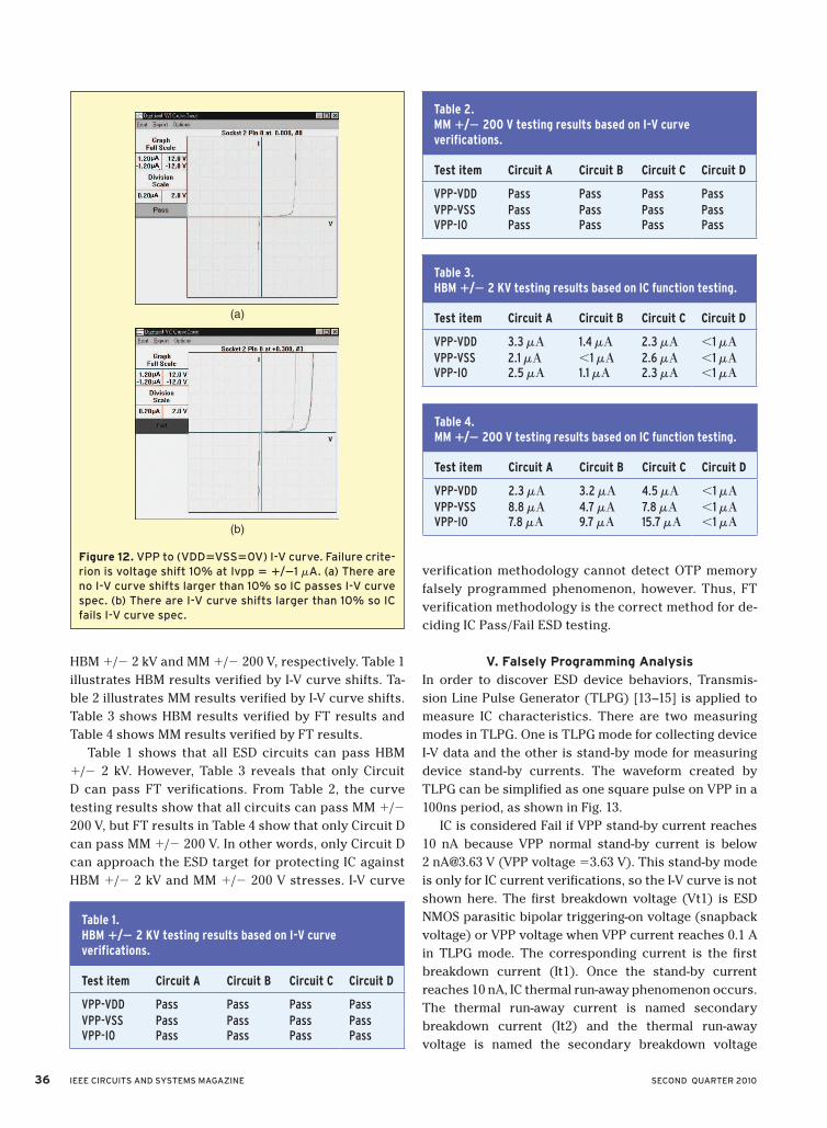
IC failure criteria depend on two types of testing
methodologies. The first method is I-V curve measure-
ment. This method has voltage test at VPP from 212 V to
112 V combined with both terminals VDD and VSS in
0 V. VPP current (Ivpp) range is measured from 21.2 mA
to 1.2 mA. If VPP voltage shift is larger than 10% at Ivpp
equal to 1 /21 mA, IC is considered Fail; otherwise, IC
is considered Pass. Fig. 12 illustrates the I-V curve mea-
sured by the machine Thermo Keytek Zapmaster. Pass
testing result is illustrated in Fig. 12 (a) and Fail testing
result in Fig. 12 (b). The second verification methodol-
ogy depends on function testing (FT) result to check
whether or not there are ESD currents entering OTP. If
the OTP cell current reaches 1 mA, IC is considered Fail;
otherwise, IC is regarded as Pass.
Two kinds of ESD events, Human Body Model (HBM)
and Machine Model (MM) are utilized in this study.
Each ESD event has both kinds of stress polarities,
positive and negative zapping. The stress voltages are
Figure 11. GDNMOST connects ESD avoiding circuit and OTP memory.
G1
C1
R1P1
N1
VPP
N2
OTP
VSS
D1
P3
N3
R3
P4
N4
VDD
VDD
ESD-Avoiding Circuit
ESD-Current Path 2
ESD-Stopping Wall
ESD-Current
Path 1
R2
36 IEEE CIRCUITS AND SYSTEMS MAGAZINE SECOND QUARTER 2010
HBM 1/2 2 kV and MM 1/2 200 V, respectively. Table 1
illustrates HBM results verified by I-V curve shifts. Ta-
ble 2 illustrates MM results verified by I-V curve shifts.
Table 3 shows HBM results verified by FT results and
Table 4 shows MM results verified by FT results.
Table 1 shows that all ESD circuits can pass HBM
1/2 2 kV. However, Table 3 reveals that only Circuit
D can pass FT verifications. From Table 2, the curve
testing results show that all circuits can pass MM 1/2
200 V, but FT results in Table 4 show that only Circuit D
can pass MM 1/2 200 V. In other words, only Circuit D
can approach the ESD target for protecting IC against
HBM 1/2 2 kV and MM 1/2 200 V stresses. I-V curve
verification methodology cannot detect OTP memory
falsely programmed phenomenon, however. Thus, FT
verification methodology is the correct method for de-
ciding IC Pass/Fail ESD testing.
V. Falsely Programming Analysis
In order to discover ESD device behaviors, Transmis-
sion Line Pulse Generator (TLPG) [13–15] is applied to
measure IC characteristics. There are two measuring
modes in TLPG. One is TLPG mode for collecting device
I-V data and the other is stand-by mode for measuring
device stand-by currents. The waveform created by
TLPG can be simplified as one square pulse on VPP in a
100ns period, as shown in Fig. 13.
IC is considered Fail if VPP stand-by current reaches
10 nA because VPP normal stand-by current is below
2 [email protected] V (VPP voltage 53.63 V). This stand-by mode
is only for IC current verifications, so the I-V curve is not
shown here. The first breakdown voltage (Vt1) is ESD
NMOS parasitic bipolar triggering-on voltage (snapback
voltage) or VPP voltage when VPP current reaches 0.1 A
in TLPG mode. The corresponding current is the first
breakdown current (It1). Once the stand-by current
reaches 10 nA, IC thermal run-away phenomenon occurs.
The thermal run-away current is named secondary
breakdown current (It2) and the thermal run-away
voltage is named the secondary breakdown voltage
Figure 12. VPP to (VDD5VSS50V) I-V curve. Failure crite-rion is voltage shift 10% at Ivpp 5 1/21 mA. (a) There are no I-V curve shifts larger than 10% so IC passes I-V curve spec. (b) There are I-V curve shifts larger than 10% so IC fails I-V curve spec.
(a)
(b)
Table 1. HBM 1/2 2 KV testing results based on I-V curve verifications.
Test item Circuit A Circuit B Circuit C Circuit D
VPP-VDD Pass Pass Pass PassVPP-VSS Pass Pass Pass PassVPP-IO Pass Pass Pass Pass
Table 2. MM 1/2 200 V testing results based on I-V curve verifications.
Test item Circuit A Circuit B Circuit C Circuit D
VPP-VDD Pass Pass Pass PassVPP-VSS Pass Pass Pass PassVPP-IO Pass Pass Pass Pass
Table 3.HBM 1/2 2 KV testing results based on IC function testing.
Test item Circuit A Circuit B Circuit C Circuit D
VPP-VDD 3.3 mA 1.4 mA 2.3 mA ,1 mAVPP-VSS 2.1 mA ,1 mA 2.6 mA ,1 mAVPP-IO 2.5 mA 1.1 mA 2.3 mA ,1 mA
Table 4.MM 1/2 200 V testing results based on IC function testing.
Test item Circuit A Circuit B Circuit C Circuit D
VPP-VDD 2.3 mA 3.2 mA 4.5 mA ,1 mAVPP-VSS 8.8 mA 4.7 mA 7.8 mA ,1 mAVPP-IO 7.8 mA 9.7 mA 15.7 mA ,1 mA

SECOND QUARTER 2010 IEEE CIRCUITS AND SYSTEMS MAGAZINE 37
(Vt2) for distinguishing them from It1
and Vt1. Table 5 lists all Vt1, It1, Vt2 and
It2 values. Fig. 14 illustrates TLPG I-V
curve results for Circuits A-D at TLPG
mode. From I-V curves, Circuits A and C
that own GGNMOST as ESD protection
circuit have ESD device snapback ef-
fects, but Circuits B and D that have
GDNMOST as ESD protection circuit do
not have such phenomena.
Since Vt1 (,2.5 V) of GDNMOST
does not reach 7 V, VPP voltage does
not necessarily reach the program-
ming voltage when ESD device turns
on. This result can reduce OTP memory
falsely programmed possibilities. It can also explain why
GDNMOST is necessary for ESD protection circuit. How-
ever, TLPG voltage keeps on increasing after VPP reaches
turn-on voltage. In Circuits B and D, VPP voltage reaches
7 V when VPP current is about 1.4 A. If VPP current is
multiplied by 1.5 kV (HBM mode equal resistor), HBM
endured voltages of IC are 2040 V and 2115 V for Circuit
B and Circuit D, respectively. VPP voltage reaches 7 V
under about 2000 V HBM stress, so ESD currents can
enter OTP cells if there are no ESD avoiding circuits for
preventing ESD currents from entering OTP cells. The
above analysis explains why only Circuit D can pass
HBM 1/2 2 kV and MM 1/2 200 V without any falsely
programmed issues.
Usually, many circuit designers add a 100 V input
resistor for preventing OTP memory from falsely
programmed. The resistor cannot be designed to be
too large; otherwise, OTP cells will encounter program
efficiency issues. When ESD event happens, only a little
ESD current can be allowed to enter OTP cells. For exam-
ple, 1 mA is the maximum current in this study. From the
Ohm rule, there is only a maximum allowable voltage 0.1
mV (100 V * 1 mA 2 on the input resistor at ESD events. Such
small voltage dropping cannot stop ESD currents entering
OTP cells, so the input resistor of Circuits B and C cannot
avoid OTP cell to have falsely programmed issues.
Briefly summarizing, for Circuits A-D,
desired ESD dissipation path is the ESD
current path 1, but ESD currents can
fl ow the ESD current path 2 to falsely
program OTP memory cells. OTP
memory cells with Circuits A and B can
be easily falsely programmed, whereas
those memory cells with Circuits
C and D are not because they have
ESD avoiding circuit forming the ESD
stopping wall. However, ESD devices of
Circuit C cannot effectively turn on to
dissipate ESD currents since Vt1 is too
large. Finally, only Circuit D that owns
ESD avoiding circuit and GDNMOST can
be chosen as ESD protection circuit for avoiding OTP
memory cells falsely programmed.
VI. Simulation Analysis
Circuit D is the only circuit that has no OTP memory
cell falsely programmed issues. In order to study the
turning-on mechanism of Circuit D, TLPG 100 ns square
Table 5. TLPG testing results and OTP memory falsely programmed list.
Circuit name
ESD protection circuit Vt1(V) It1(A) Vt2(V) It2 (A)
Ivpp (A) at VPP57 V
Ivpp (at 7V) 3 1.5 V k(V)
Falsely programmed
Circuit A GGNMOST 8.8 0.056 9.5 4.18 0.003 4.5 V
Circuit B GDNMOST 2.2 0.1 9.6 3.45 1.36 2040 V
Circuit C GGNMOST 1 ESD avoiding
8.9 0.006 10.7 3.97 0.002 3 V
Circuit D GDNMOST 1 ESD avoiding
2.3 0.101 10.2 3.94 1.41 2115 X
Figure 14. TLPG I-V curves of four kinds of VPP circuits.
0 2 4 6 8 10 12
0
1
2
3
4
5
Circuit A:
GGNMOST
Circuit B:
GDNMOST
Circuit C:
GGNMOST + ESD Avoiding
Circuit D:
GDNMOST + ESD Avoiding
Devic
e U
nder
Test C
urr
ent (A
)
Device Under Test Voltage (V)
Figure 13. Ideal transmission line pulse generator (TLPG) square pulse in 100-ns pe-riod.
Stress Pulse Time (ns)50 100 150
Str
ess P
uls
e V
oltage (
V)

38 IEEE CIRCUITS AND SYSTEMS MAGAZINE SECOND QUARTER 2010
pulse shown in Fig. 13 is used to simulate Circuit D
behaviors and H-spice is taken as the simulation tool.
ESD event “VPP-VSS” is considered again. VPP tied to 7 V
is considered as the simulation condition because OTP
memory programmed voltage is 7 V. VPP is at 7 V and
VSS is at 0 V, so floating terminal VDD coupled voltage is
decided ideally by PMOS and NMOS size ratio through
the inverter P3/N3, obeying the following equation:
VDD5 VPP 3P3
P31 N35 7 V 3
2
21 40 6 0.33 V. (1)
The above description illustrates the ideal charge
coupled result, but terminal VDD coupled voltage
does not follow the above ideal equation. According
to the charge coupled effect, VDD coupled voltage
is considered having four kinds of values. The first
condition is considering VDD coupled voltage as 0 V if
terminal VDD is coupled to terminal VSS only; the second
is VDD coupled voltage in 0.33 V from the ideal charge
coupled equation; the third is VDD coupled voltage in 0.7
V if a little more charges are coupled to terminal VDD;
the last condition is VDD coupled voltage in 1V if a lot of
charges are coupled to terminal VDD.
The simulation program operat es in four time divisions
because of four kinds of VDD estimated voltages. Each
time division has both rise time and fall time equal to 10
ns. From Fig. 15, one can see that if VDD coupled voltage
is equal to 0 V, 0.33 V or 0.7 V, OTP memory voltage is
about 3.9 V, much less than 7 V, so there are no falsely
programmed events in OTP memories. However, if termi-
nal VDD is coupled to 1V, OTP memories can reach 7 V
and thus they can be falsely programmed. This is because
the threshold voltage range of NMOS transistor is from
0.65 V to 0.95 V.
There is no falsely programmed issue
in Circuit D, so VDD coupled voltage is
below 1 V under HBM 1/2 2k V and MM
1/2 200 V stresses in this study. Based
on the above analyses, the coupled
charge from terminal VPP to terminal
VDD is very important under ESD
stresses. P3 size must be kept as small
as possible as compared to N3 size, so
that P3 can turn on and then turn off
transistor P4 under ESD stresses.
VII. Conclusions
Transmission gate N/PMOS transistors
are the normal I/O circuits for signal
controls, but no circuit designers use
them for stopping ESD currents. In
this study, since OTP memory cells
are so sensitive to ESD currents, the
transmission N/PMOS transistors are adopted for
preventing ESD currents from entering OTP memory
cells. They are combined with one control inverter for
forming the ESD avoiding circuit. Furthermore, in order
to make ESD protection devices turn on at a smaller
voltage, Gate-Driven circuit is used. If both Gate-Driven
circuit and ESD avoiding circuit are adopted, there will
be no OTP memory cell falsely programmed issues. Cir-
cuit designers can use the same technique to increase
ICs’ reliabilities. The transmission N/PMOS transistors
controlled under the inverter not only stop ESD currents
entering memories, but also work for preventing other
unpredicted events from damaging IC, such as noise.
Acknowledgments
The authors wish to thank Shine Chung of Taiwan Semi-
conductor Manufacturing Company for helpful data
analyses. They also would like to thank Tien-Hao Tang
of United Microelectronics Corporation and Jian-Hsin
Lee for TLPG measurements.
Shao-Chang Huang received the B.S.
and M.S. degrees in electrical engineer-
ing from the National Cheng Kung Uni-
versity, Tainan, Taiwan, in 1994 and
1996, respectively.
From 1996 to 1998, he was an officer
in national compulsory military service.
From 1998 to 1999, he was engaged in thin-film-transistor
device at ERSO in ITRI, Taiwan. From 1999 to 2006, he
worked on ESD/Latch-up/IO research in UMC, Ltd., HBA,
Ltd., TSMC, Ltd. and NOVATEK, Ltd. As a UMC engineer,
he worked on 90nm process ESD solutions at IBM, Fish-
kill, N.Y. in 2001. Since the end of 2006, he joined eMemory
Figure 15. GDNMOST and ESD avoiding circuit simulation results at VPP in 7V.
8.0
7.0
6.0
5.0
4.0
3.0
Voltage (
V)
2.0
1.0
0.0
–1.00.0N
C1: 61.84211N
200.
0 N
300.
0 N
400.
0 N
500.
0 N
600.
0 N
700.
0 N
800.
0 N
Time (s)
Y1
7.00000 7.00000 7.00000 7.00000
V (VPP)V (VDD)V (OTP)
7.00000
3.859833.898303.89720
0.000000.33000
0.700001.00000

SECOND QUARTER 2010 IEEE CIRCUITS AND SYSTEMS MAGAZINE 39
Technology, Taiwan, where he is currently the ESD/ IO de-
partment manager. He is the author or coauthor of more
than 8 papers published in journals and conferences, and
he holds more than 20 patents. His current research in-
terests include ESD/Latch-up devices and circuits, and
I/O related circuits.
Ke-Horng Chen (M’04-SM’09) received
the B.S., M.S., and Ph.D. degrees in elec-
trical engineering from the National Tai-
wan University, Taipei, Taiwan, in 1994,
1996, and 2003, respectively.
From 1996 to 1998, he was a part-
time IC Designer at Philips, Taipei. From
1998 to 2000, he was an Application Engineer at Avanti,
Ltd., Taiwan. From 2000 to 2003, he was a Project Man-
ager at ACARD, Ltd., where he was engaged in design-
ing power management ICs. He is currently an Associate
Professor in the Department of Electrical Engineering,
National Chiao Tung University, Hsinchu, Taiwan, where
he organized a Mixed-Signal and Power Management IC
Laboratory. He is the author or coauthor of more than
80 papers published in journals and conferences, and
he holds several patents. His current research interests
include power management ICs, mixed-signal circuit
designs, display algorithm and driver designs of liquid
crystal display (LCD) TV, RGB-color sequential backlight
designs for optically compensated bend (OCB) panels,
and low-voltage circuit designs.
Hsin-Ming Chen received the B.S. and
M.S. degrees in electrical engineering
from the National Tsing Hua Univer-
sity, Hsinchu, Taiwan, in 1994 and 1996,
respectively.
From 1996 to 1998, he was an officer
in national compulsory military service.
From 1998 to 2002, he worked on Nonvolatile Memory
and Cu/LK process development at TSMC. Since 2002,
he joined eMemory Technology, Taiwan, where he is
currently the deputy director working on embedded
memory technology development. He is the author or
coauthor of 5 papers published in journals and confer-
ences, and he holds more than 20 patents.
Ming-Chou Ho received the B.S. and
M.S. degrees in electrical engineering
from the National Tsing Hua Univer-
sity, Hsinchu, Taiwan, in 1992 and 1994,
respectively.
From 1994 to 1996, he was an officer
in national compulsory military service.
From 1996 to 2002, he was an engineer at TSMC, Ltd.,
where he was engaged in IC process integrations. Since
2002, he joined eMemory Technology, Taiwan, where he
is currently the sales director. He works on Non-Volatile
Memory device and technology development. He is one in-
ventor of key embedded NVM technologies and obtained
the 2005 National Invention and Creation Award in Taiwan.
He is the author or coauthor of more than 30 patents.
Rick Shih-Jye Shen received the B.S.
and Ph.D. degrees in electrical engineer-
ing from the National Tsing Hua Univer-
sity, Hsinchu, Taiwan, in 1992 and 1998,
respectively.
From 1998 to 2000, he was an officer
in national compulsory military service.
From 2000 to 2001, he was an engineer at TSMC, Ltd.,
where he was engaged in IC process integration. Since
2001, he joined eMemory Technology, Taiwan. He works
for Non-Volatile Memory device and technology devel-
opment. He is one inventor of key embedded NVM tech-
nologies and obtained the 2005 National Invention and
Creation Award in Taiwan. He is the author or coauthor
of more than 10 papers published in journals and confer-
ences, and he holds more than 110 patents.
References[1] S. Shukuri, K. Yanagisawa, and K. Ishibashi, “CMOS process compat-
ible ie-Flash (inverse gate electrode Flash) technology for system-on-a
chip,” in Proc. IEEE Custom Integrated Circuits Conf., 2001, pp. 179–182.
[2] J.-I. Miyamoto, J.-I. Tsujimoto, N. Matsukawa, S. Morita, K. Shinada,
H. Nozawa, and T. Iizuka, “An experimental 5-V-only 256-kbit CMOS EE-
PROM with a high- performance single-polysilicon cell,” IEEE J. Solid-
State Circuits, vol. sc-21, pp. 852–860, Oct. 1986.
[3] B. Carney, E. Lucero, R. Mendel, and H. Reiter, “Confi gurable EE-
PROMS for ASICS,” in Proc. IEEE Custom Integrated Circuits Conf., 1988,
pp. 4.2.1–4.2.4.
[4] R. J. McPartland and R. Singh, “1.25 volt, low cost, embedded FLASH
memory for low density applications,” in Symp. on VLSI Circuits Dig. of
Technical Papers, 2000, pp. 158–161.
[5] R. S. C. Wang, R. S. J. Shen, and C. C. H. Hsu, “Neobit – high reliable log-
ic non-volatile memory (NVM),” in Proc. of 11th IPFA, 2004, pp. 111–114.[6] S.-C. Huang, K.-H. Chen, and H.-M. Chen, “Electrostatic discharge
avoiding circuit,” U.S. Patent Application 20080316660, June 20, 2007.
[7] C.-H. Hsu, S.-J. Shen, and M.-C. Ho, “Semiconductor memory device
having improved data retention,” U.S. Patent 6 914 825, July 5, 2005.
[8] C.-J. Huang, Y.-M. Hsu, and J.-H. Huang, “Pure CMOS latch-type fuse
circuit,” U.S. Patent 6 914 842, July 5, 2005.
[9] eMemory datasheet, EO01X32GCL2_1.0.[10] R. C. Steele, “Power-up reset circuit,” U.S. Patent 4 983 857, Jan. 8, 1991.
[11] A. Amerasekera, V. Gupta, K. Vasanth, and S. Ramaswamy, “Analysis
of snapback behavior on the ESD capability of sub-0.20 mm NMOS,” in
Proc. 37th Annu. Int. Reliability Physics Symp., 1999, pp. 159–166.
[12] “Electrostatic discharge (ESD) sensitivity testing human body
model (HBM),” JESD22-A114D, Mar. 2006.[13] N. Khurana, T. Maloney, and W. Yeh, “ESD on CHMOS devices –
equivalent circuits, physical models and failure mechanisms,” in Proc.
Int. Radiation Physics Society Conf., 1985, pp. 212–223.
[14] M. T. Lee, C. H. Liu, C.-C. Lin, J.-T. Chou, H. T. H. Tang, Y. J. Chang,
and K. Y. Fu, “Comparison and correlation of ESD HBM (human body
model) obtained between TLPG, wafer-level, and package-level tests,”
in Proc. EOS/ESD Symp., 2000, pp. 105–110.[15] R. A. Ashton, “Transmission line pulse measurements: A tool for
developing ESD robust integrated circuits,” in Proc. Int. Conf. on Micro-
electronic Test Structures, vol. 17. 2004.