Embed Size (px)
Citation preview


INTERFACING
8255: Programmable Peripheral Interface
or Programmable Input output Device

INTERFACING
Introduction
METHODS OF DATA TRANSFER
Simple Input and Output
Simple Strobe Input/ Output
Single Handshake data transfer
Double Handshake data transfer

INTERFACING
Simple Input and Output
I/O operations are not directly dependent on any other signals.For Example: Reading data from thermostat; it is simple connected to input
port line and processor simply reads the port, as data is always available and
ready so it can be read any time.
The crossed lines on the waveform represents time at which databyte is available at the port
INTERFACING
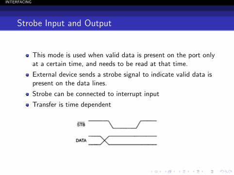
Strobe Input and Output
This mode is used when valid data is present on the port onlyat a certain time, and needs to be read at that time.
External device sends a strobe signal to indicate valid data ispresent on the data lines.
Strobe can be connected to interrupt input
Transfer is time dependent

INTERFACING
Strobe Input and Output
High speed data transfer not possible
data rates of sending system and receiving system can bedi↵erent
to avoid this HANDSHAKE data transfer is used

INTERFACING
Single handshake I/O
Handshake Data Transfer
Peripheral device outputs some data and sends strobe signalto processor
Processor detects strobe on poll or interrupt basis and readsthe data
Also it sends an Acknowledge signal to device indicating thatdata has been read and next byte of data can be sent.

INTERFACING
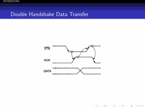
Double Handshake Data Transfer
Used where more co-ordination is required
INTERFACING
Double Handshake Data Transfer

INTERFACING
Handshaking is a good idea but uses too much processor time,so parallel port devices such as 8255 are used to automatically
manage handshake operation.
INTERFACING
8255 Programmable Peripheral Interface
It is a programmable parallel I/O device
40 pin IC
24 programmable I/O pins arranged as two 8-bit ports andtwo 4-bit ports
It has Three 8-bit ports: Port A,Port B and Port C, which arearranged in two groups of 12 pins
Control register defines the functions of each I/O port and inwhich mode they should operate

INTERFACING
Pin Diagram
INTERFACING
Pin Diagram Description
PA0- PA7 : Port A; 8-bit bidirectional I/O pins
PB0- PB7 : Port B; 8-bit bidirectional I/O pins
PC0- PC7 : Port C; 8-bit bidirectional I/O pins. These can evenbe used as two 4-bit ports (PC0 � PC3 andPC4 � PC7) , Also used to produce handshake signalsfor A and B
D0 � D7 : 8-Bit bi-directional data bus connected to processor
RESET : When reset clears control word and all ports
RD : Read, active low input line used to read data fromprocessor
WR : Write, active low input line used to send data toprocessor

INTERFACING
Pin Diagram Description
A0 � A1 : Address Lines; used to select ports of 8255
A0 A1 Selected Port0 0 Port A0 1 Port B1 0 Port C1 1 Control Register

INTERFACING
8255 Functional Block Diagram
INTERFACING
8255 Operational Modes and Initialization
MODE 0
simple input or output without handshaking
If Port A and B are initialized in mode 0, port C can be usedas 8-bit port
If port C lines are used as output, individual bits can be setand reset by special control word
Two halves of port C (4-bits)are independent
One can be used as input and other as output

INTERFACING
8255 Operational Modes and Initialization
MODE 1
Use port a or B as handshake(strobed) input/output
PC0,PC1,PC2 lines of port C are used as handshake lines forport B
PC3,PC4,PC5 lines of port C are used as handshake lines forport A(input port)
PC6,PC7 lines are used as input output lines
PC3,PC6,PC7 lines of port C are used as handshake lines forport A(output port)
PC4,PC5 lines are used as input output lines

INTERFACING
8255 Operational Modes and Initialization
MODE 2
Bi-directional handshake data transfer
Data can be output or input on the same eight lines
If port A is used in mode 2 :PC3 to PC7 are used as handshake line for port APC0 to PC2 can be used as I/O pins if Port B is in Mode 0Or PC0 to PC2 are used as port B handshake if Port B is inMode 1

INTERFACING
8255 Control word (8-bit)
There are two types of Control word:
The MSB tells which control word is being sent
1 Mode definition control word (if MSB = 1)
2 Port C bit set/reset control word (if MSB = 0)

INTERFACING
Mode definition control word (if MSB = 1)
INTERFACING
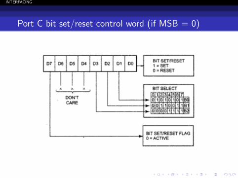
Port C bit set/reset control word (if MSB = 0)

INTERFACING
8254 Software Programmable Timer/Counter
Why 8253/8254?
Since, it is not possible to generate accurate time delays Using delay
subroutines in 8086.
8254/8253 facilitates:
Accurate time delays
Minimizes load on processor
real time clock
event counter
square wave generator
complex waveform generator
INTERFACING
8254/8253
Software Programmable Timer/Counter means, we can load countin them, start them and stop them with instructions in theprogram.To program such device, COUNT BYTES and CONTROL BYTEShave to be sent to the timer/counter peripheral device

INTERFACING
8254 vs 8253
8253 8254clock frequency 2.6MHz clock frequency 8MHz
No read back feature Read back feature
Read back feature allows to latch the count in all counters and the status of
counters at any point.

INTERFACING
Features of 8254
Three independent 16-bit down counters.
8254 can handle inputs from DC to 10 MHz (5MHz 8254-5,8MHz 8254, 10MHz 8254-2) where as 8253 can operate upto2.6 MHz
Three counters are identical presettable, and can beprogrammed for either binary or BCD count.
Counter can be programmed in six di↵erent modes.
Compatible with all Intel and most other microprocessors.
8254 has powerful command called READ BACK commandwhich allows the user to check the count value, programmedmode and current mode and current status of the counter.

INTERFACING
8254 block diagram

INTERFACING
8254 block diagram
Data Bus Bu↵er :
Bi-directional, 8-bit bu↵er is used to interface the 8253/54 tothe system data bus.
The Data bus bu↵er has three basic functions:Programming the modes of 8253/54.Loading the count registers.Reading the count values.

INTERFACING
8254 block diagram
Read/Write Logic : The Read/Write logic has five signals :RD,WR , CS and the address lines A0 and A1
In the peripheral I/O mode, the RD, and WR signals areconnected to IOR and IOW , respectively. In memory-mappedI/O, these are connected to MEMR and MEMW
INTERFACING
8254 block diagram
Control Word Register :
This register is accessed when lines A0 and A1 are at logic 1
used to write a command word which specifies the counter tobe used (binary or BCD), its mode, and either a read or writeoperation.

INTERFACING
8254 block diagram
Counters :
These three functional blocks are identical in operation.
Each counter consists of a single, 16 bit, pre-settable, downcounter.
Can operate in either binary or BCD
Its input, gate and output are configured by the selection ofmodes stored in the control word register
Programmer can read the contents of any of the threecounters without disturbing the actual count in process

INTERFACING
8254 block diagram
Counters :
CLK : Signals of frequency between 0 to 8 MHz can beapplied as input to these 3 pins
GATE : Allows to start or stop the counter with an externalhardware signal. If GATE = 1, counter is enabled forcountig and if GATE = 0 it is disabled.
OUT : Output signal of each counter appears on this pin.

INTERFACING
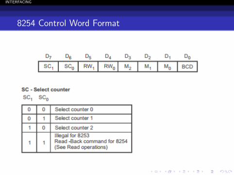
8254 Control Word Format
INTERFACING
8254 Control Word Format

INTERFACING
8254 Control Word Format

INTERFACING
8254 Control Word Format

INTERFACING
8254 Control Word Format

INTERFACING
8254 Counter Modes
1 Mode 0 (Interrupt On Terminal Count )
2 Mode 1 (Hardware retriggerable Monoshot )
3 Mode 2 (Timed interrupt Generator )
4 Mode 3 (Square Wave Generator )
5 Mode 4 (Software Triggered Strobe )
6 Mode 5 (Hardware Triggered Strobe )

INTERFACING
Mode 0 (Interrupt On Terminal Count )
The output becomes a logic 0 when the control word iswritten remains low even after count value loaded in counter.
Counter starts decrementing after falling edge of clock TheOUT goes high upon reaching the terminal count and remainshigh till reloading OUT can be used as interrupt
Writing a count register , when previous counting is in processfirst byte when loaded stops the previous count,second byte when loaded starts new count
Gate high = normal counting
Gate low = counting terminated and current count latched tillGATE goes high again

INTERFACING
Mode 0 (Interrupt On Terminal Count )
Assuming, CW = 10 ; counter 0 initialized for binary counting,mode 0 and read/write of only LSB

INTERFACING
Mode 0 (Interrupt On Terminal Count )
When GATE = 0, counter is held and when GATE = 1, countercontinues
INTERFACING
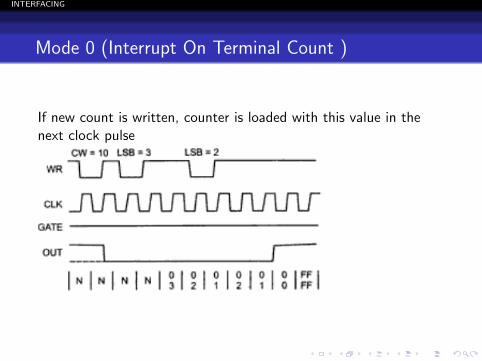
Mode 0 (Interrupt On Terminal Count )
If new count is written, counter is loaded with this value in thenext clock pulse

INTERFACING
Mode 1 (Hardware retriggerable Monoshot )
Gate input is used as trigger input
Output remains high till the count is loaded after applicationof trigger, output goes low and remains low till count becomeszero
Another count loaded, when output already low, it does notdisturb counting until a new trigger is applied at the gate
New counting starts after new trigger pulse

INTERFACING
Mode 1 (Hardware retriggerable Monoshot )
For mode 1 GATE act as trigger input, When GATE =1 count istransferred from count register to actual counter

INTERFACING
Mode 1 (Hardware retriggerable Monoshot )
This waveform demonstrates retriggerable behaviorIf another trigger pulse comes,the count is reloaded and output willremain low

INTERFACING
Mode 1 (Hardware retriggerable Monoshot )
New count will not be loaded

INTERFACING
Do it yourself
Assignment - 2
Study all the other 5 modes and prepare a document which willcontain theory and related figures.