Embed Size (px)
Citation preview

ENGINEERING.
1
FEDERAL UNIVERSITY OYE EKITI
FACULTY OF ENGINEERING
DEPARTMENT OF ELECTRICAL AND ELECTRONICS
PRACTICAL MANUAL
for
EEE 311- Electrical Engineering Practical – I
Coordinated By: Dr. Engr. A.M Zungeru
2
INTRODUCTION
The place of laboratory work in Electrical and Electronic Engineering is very
important. Laboratory course work enables students to do experiments on the
fundamental laws and principles encountered in the theoretical work. In these
formative years the student is made to identify a wide range of electrical
components, measure their values thereby learning to handle instruments and
equipments and to appreciate their limitations. Students are also made to learn how
to bread board, connect simple circuits and verify the simple laws of Ohms’
Kirchhoff ’s Current and Voltage Laws, Thevenin’s, Norton’s, and others who
have contributed immensely on the formulation of laws and theories. Other aspect
of Electrical and Electronic practical were all dealt with.
It may also be observed that the background information to every experiment is the
‘theory’ aspect and it is quit lengthy in many cases. It is aimed at ensuring that the
students are sufficiently familiar with the theoretical aspect of the experiment and
consequently sharpen their focus on the results expected.
The laboratory exercises in this manual are designed to provide a working
knowledge of some of the more fundamental principles of Electrical, Electronic an
d Computer Engineering. All the experiments on this handbook were simulated to
get the response of each circuit, and were all found working properly as expected.
While working through the manual the student will become more familiarize with
the manual and the basic theories in Electrical and Electronic Engineering.
In order to fully understand the principle being investigated, the student is advised
to read extensively in the related topics before entering the laboratory. At the end
of each laboratory, questions and exercises should be completed and returned to
the Examiner for proper grading as scheduled.

3
GENERAL LABORATORY SAFETY
Safety is an important factor in any laboratory work. It should be understood that
any use of electricity inherently involves some degree of safety hazard. The best
way to achieve safety in the use of electrical equipment is to adhere to all the
safety rules which include;
1. Understanding equipment you are proposing to use and its rating,
2. Understanding the application to which the equipment is to be use for,
3. Ensuring that all reasonable safety measures are followed,
4. Taking no chance, nor short cut, in safety procedures.
4
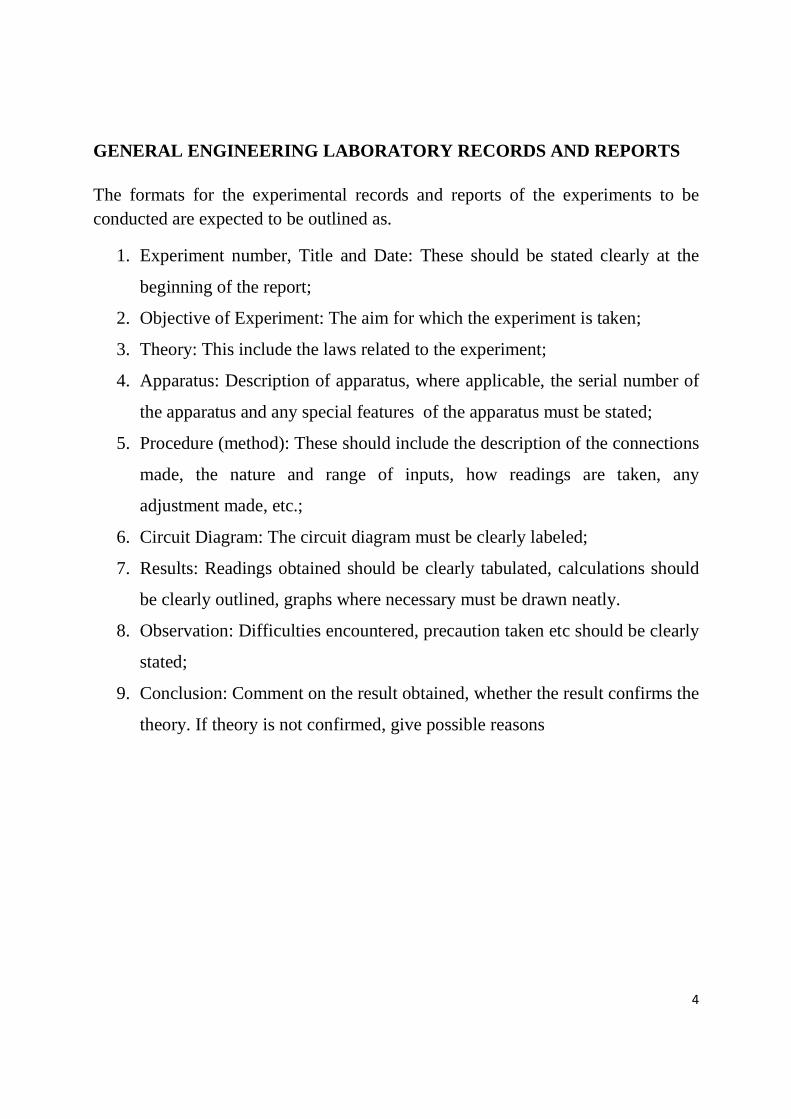
GENERAL ENGINEERING LABORATORY RECORDS AND REPORTS
The formats for the experimental records and reports of the experiments to be conducted are expected to be outlined as.
1. Experiment number, Title and Date: These should be stated clearly at the
beginning of the report;
2. Objective of Experiment: The aim for which the experiment is taken;
3. Theory: This include the laws related to the experiment;
4. Apparatus: Description of apparatus, where applicable, the serial number of
the apparatus and any special features of the apparatus must be stated;
5. Procedure (method): These should include the description of the connections
made, the nature and range of inputs, how readings are taken, any
adjustment made, etc.;
6. Circuit Diagram: The circuit diagram must be clearly labeled;
7. Results: Readings obtained should be clearly tabulated, calculations should
be clearly outlined, graphs where necessary must be drawn neatly.
8. Observation: Difficulties encountered, precaution taken etc should be clearly
stated;
9. Conclusion: Comment on the result obtained, whether the result confirms the
theory. If theory is not confirmed, give possible reasons
5
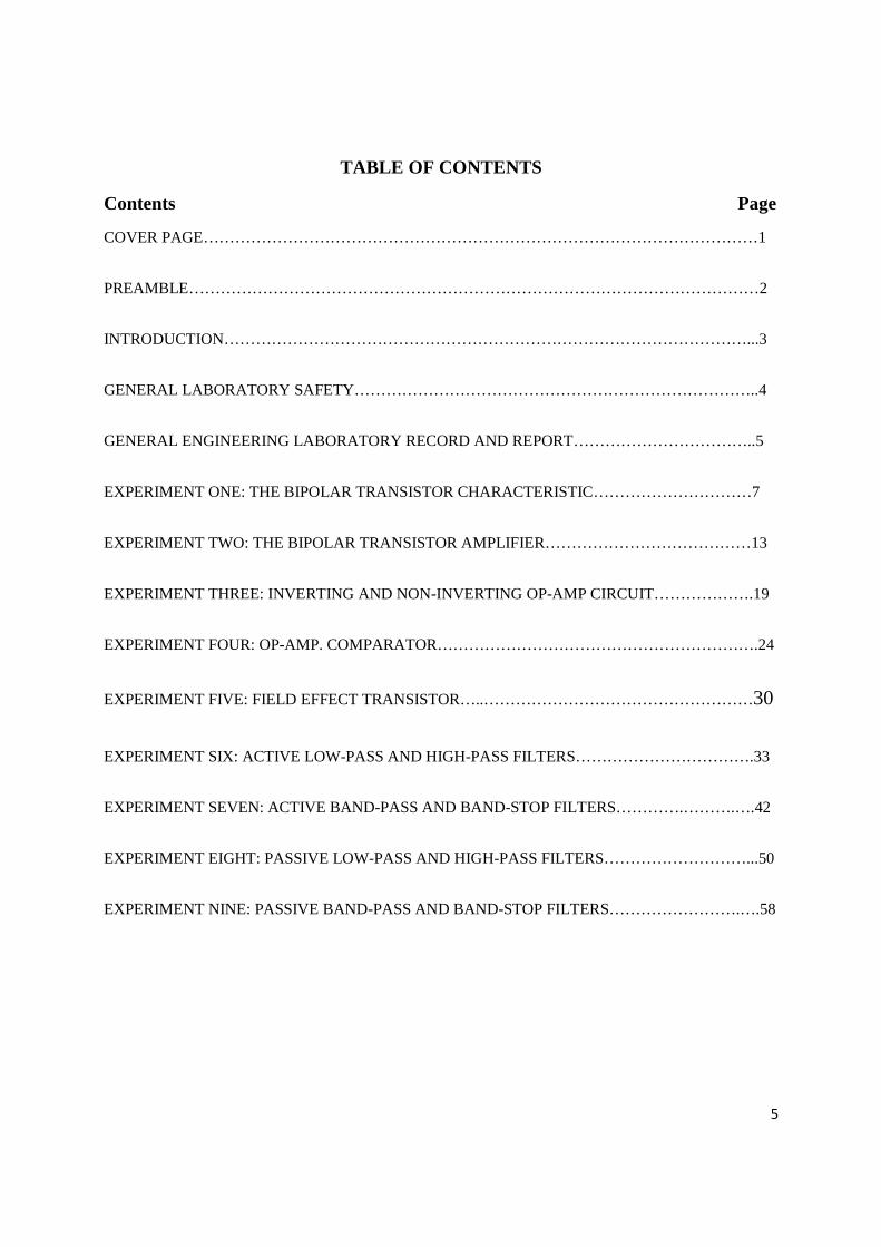
TABLE OF CONTENTS
Contents Page
COVER PAGE……………………………………………………………………………………………1
PREAMBLE………………………………………………………………………………………………2
INTRODUCTION………………………………………………………………………………………...3
GENERAL LABORATORY SAFETY…………………………………………………………………..4
GENERAL ENGINEERING LABORATORY RECORD AND REPORT……………………………..5
EXPERIMENT ONE: THE BIPOLAR TRANSISTOR CHARACTERISTIC…………………………7
EXPERIMENT TWO: THE BIPOLAR TRANSISTOR AMPLIFIER…………………………………13
EXPERIMENT THREE: INVERTING AND NON-INVERTING OP-AMP CIRCUIT……………….19
EXPERIMENT FOUR: OP-AMP. COMPARATOR…………………………………………………….24
EXPERIMENT FIVE: FIELD EFFECT TRANSISTOR…..……………………………………………30
EXPERIMENT SIX: ACTIVE LOW-PASS AND HIGH-PASS FILTERS…………………………….33
EXPERIMENT SEVEN: ACTIVE BAND-PASS AND BAND-STOP FILTERS………….……….….42
EXPERIMENT EIGHT: PASSIVE LOW-PASS AND HIGH-PASS FILTERS………………………...50
EXPERIMENT NINE: PASSIVE BAND-PASS AND BAND-STOP FILTERS…………………….….58

6
INSTITUTION:------------------------------------------------------------------------------------------------------
DEPARTMENT:----------------------------------------------------------------------------------------------------
STUDENTS’S NAME: ----------------------------------------------REG/MAT NO: ------------------
GROUP NO: -----------------------------------------------------------DATE: ----------------------------------
INSTRUCTOR’S NAME: ------------------------------------------SIGNATURE: ---------------------

7
EXPERIMENT ONE: THE BIPOLAR TRANSISTOR CHARACTERIST ICS
1.0 OBJECTIVES:
(1) The bipolar transistor.
(2) The bipolar transistor characteristics.
(3) Operating line and operating point.
1.1 EQUIPMENT REQUIRED
TPS-3321 Power supply A multimeter Banana wires Transistor 1N2222 Resistors: 100Ω, 1kΩ, 10kΩ, 91kΩ
1.2 PROCEDURE
Step 1: Connect TPS-3321 trainer to the power supply and connect the power supply to the Mains.
Step 2: Implement the following circuit on the main plug in board.
Fig 1.0
1K
+12V
VC
IC
VE
100
IE
VB 10K
VS
8
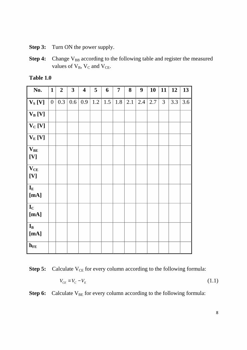
Step 3: Turn ON the power supply.
Step 4: Change VBB according to the following table and register the measured values of VB, VC and VCE.
Table 1.0
13 12 11 10 9 8 7 6 5 4 3 2 1 No.
3.6 3.3 3 2.7 2.4 2.1 1.8 1.5 1.2 0.9 0.6 0.3 0 VS [V]
VB [V]
VC [V]
VE [V]
VBE [V]
VCE [V]
IE [mA]
IC [mA]
IB [mA]
hFE
Step 5: Calculate VCE for every column according to the following formula:
ECCE VVV −= (1.1)
Step 6: Calculate VBE for every column according to the following formula:

9
EBBE VVV −= (1.2)
Step 7: Calculate IE for every column according to the following formula:
E
EE R
VI = (1.2)
Step 8: Calculate IC for every value of VC according to the following formula:
= − (1.3)
Step 9: Calculate IB for every column according to the following formula:
B
BB R
VI = (1.4)
Step 10: Calculate ℎ = for each column in the table.
Step 11: Plot your results on the following graph.
Fig 1.1
Step 12: Mark the three region on the graph:
• The cutoff region. • The linear region. • The saturation region.
Step 13: Plot your results on the following graph.
IC
0 0 IB

10
Fig 1.2
Step 14: Mark the three regions on the graph:
• The cutoff region. • The linear region. • The saturation region.
Step 15: Implement the following circuit on the main plug in board.
Fig 1.3
IC
0 0 VCE
R2
R1
+12V
RC
VC
VB
VE
RE
1K 91K
2N2222
100ΩΩΩΩ 10K

11
Step 16: Measure VB, VC and VCE.
Step 17: Calculate = − (1.5)
Step 18: Mark the operating point on the graph that you plotted in step 13.
Step 19: Implement the following circuit on the main plug in board.
Fig 1.4
Step 20: Measure VB, VC and VCE.
Step 21: Calculate IC = (VCC - VC) / RC.
Step 22: Mark the operating point on the graph that you plotted in step 13.
R2
R1
+12V
RC
VC
VB
VE
1K 91K
2N2222
10K
12
EXPERIMENT REPORT: 1) Write the name of each experiment and draw below the electronic circuit.
For each circuit include the experiment measurements, results and graphs.
2) Compare between the preliminary questions and the examples with the measurement results.
13
EXPERIMENT TWO: THE BIPOLAR TRANSISTOR AMPLIFIER
1.0 OBJECTIVES
1. Amplifier gain measurement.
2. Input impedance measurement.
3. Output impedance measurement.
4. Phase shift measurement.
1.1 EQUIPMENT REQUIRED
• TPS-3321 • Power supply • A Multimeter • An oscilloscope • Banana wires • A transistor 2N2222 • Resistors: 100Ω, 1kΩ, 5.1kΩ, 10kΩ, 91kΩ • Capacitor: 10µF
1.2 PROCEDURE
Step 1: Connect TPS-3321 trainer to the power supply and connect the power supply to the Mains.

14
Step 2: Implement the following circuit on the main plug in board.
Fig 2.0
Step 3: Turn ON the power supply.
Step 4: Measure VB, VC, VCE and VE.
Step 5: Calculate IC:
= − = 12 − 1000 (2.1)
Step 6: Plot the operating line and the operating point on the graph.
Fig 2.1
Step 7: Connect the function generator output probe to the VS point.
Step 8: Connect the scope probe CH1 to the function generator output. To calculate the amplifier’s parameters, it does not matter if we use Vpeak or Vp-p or an effective voltage as long as we are consistent.
IC
EC
CC
RR
V
++++
VC
VCC VCE
+12V
R1 RC
R2 RE
VS RS
VCE VC
5.1K VE

15
Note: To annotate AC parameters we use small letters.
We use the 1kΩ resistor as the RS resistance.
Use the following h parameter values for your calculations:
Hfe = 100, hie = 2KΩ, hoe
1 = 40KΩ
CE Amplifier:
Step 9: Connect a by-pass capacitor of 10 µF parallel to RE thus short circuiting the AC voltages RE. We do not short circuit RE in order not to change its DC operating point.
Step 10: Adjust the function generator to generate a 1 Vp-p 1KHz sine wave.
Step 11: Connect the CH2 probe to the VC point.
Step 12: Calculate and record the AV, AI, Ri, Ro according to h parameter model.
Step 13: Measure the voltages VC (Vo), VRS and Vi.
Step 14: Calculate and record the AV, AI, Ri according to your measurements.
Step 15: Check the phase shift between the output and the input.
Step 16: Compare the amplifier calculation characteristics and the measurement characteristics.
CE Amplifier with RE:
Step 17: Disconnect the by-pass capacitor of RE.
Step 18: Adjust the function generator to generate a 1 Vp-p 1KHz sine wave.
Step 19: Calculate and record the AV, AI, Ri according to h parameter model.
Step 20: Measure the voltages VC (Vo), VRS and Vi.
Step 21: Calculate and record the AV, AI, Ri according to your measurements.

16
Step 22: Check the phase shift between the output and the input.
Step 23: Compare the amplifier calculation characteristics and the measurement
characteristics.
Emitter Follower Amplifier:
Step 24: Connect the CH2 probe to point VE.
Step 25: Calculate and record the AV, AI, Ri according to h parameter model.
Step 26: Measure the voltages VE (Vo), VRS and Vi.
Step 27: Calculate and record the AV, AI, Ri according to your measurements.
Step 28: Check the phase shift between the output and the input.
Step 29: Compare the amplifier calculation characteristics and the measurement
characteristics.
CB Amplifier:
Step 30: Implement the following circuit.
Fig 2.2
+12V
R1
RC
5.1K
R2
RE
VCE
VC
VS VE RS
100ΩΩΩΩ
Vo

17
Step 31: Adjust the function generator to generate a 1 Vp-p 1KHz sine wave.
Step 32: Connect the CH2 probe to point VC.
Step 33: Calculate and record the AV, AI, Ri according to h parameter model.
Step 34: Measure the voltages VC (Vo), VRS and Vi.
Step 35: Calculate and record the AV, AI, Ri according to your measurements.
Step 36: Check the phase shift between the output and the input.
Step 37: Compare the amplifier calculation characteristics and the measurement characteristics.
EXPERIMENT REPORT: 1) Write the name of each experiment and draw below the electronic circuit.
For each circuit include the experiment measurements, results and graphs.
2) Compare between the preliminary questions and the examples with the measurement results.
18
EXPERIMENT THREE: INVERTING AND NON INVERTING OP-AM P
CIRCUITS
3.0 OBJECTIVE To demonstrate the operation of both inverting and non-inverting amplifier
circuits, using a 741 operational amplifier. Both circuits operate in the closed-loop
mode.
3.1 MATERIALS Resistors (1/2 W): 1k; 4.7k; (2) 10k; 22k; 47k; 100k
741 op-amp (8-pin mini-DIP)
Two 0-15 v dc power supplies
Signal generator
Dual trace oscilloscope
Breadboard.
3.2 PREPARATION The inverting amplifier’s closed-loop (voltage) gain can be less than, equal to, or greater than 1. As its name implies, its output signal is always inverted with respect to its input signal. On the other hand, the non-inverting closed-loop (voltage) gain is always greater than 1; while the input and output signal are always in-phase. Inverting amplifier closed-loop voltage gain
Av = (3.1)
Non-inverting amplifier closed-loop voltage gain
Av = 1 + ⁄ (3.2)

19
Fig. 3.0: Inverting Amplifier Circuit
Fig. 3.1: Non inverting Amplifier Circuit
U1
741
3
2
4
7
6
51R1
10kOhm_5%
R21.0kOhm_5%
XFG1
A BT
G
XSC1
V1
15V
V2
15V
15v -15v
R3
1kohm
U1
741
3
2
4
7
6
51
R1
1 0kOhm_5%R21.0kOhm_5%
XFG1 A BT
G
XSC1
V1
15V
V2
15V
15v -15v
R3
100kohm
20
3.3 PROCEDURE STEP 1: Wire the inverting amplifier circuit shown in the schematic diagram of
fig 3.0, and set your oscilloscope for the following settings: Channels 1
and 2: 5 v/ division, ac coupling Time base: 1 ms/division
STEP 2: Apply power to the breadboard, and adjust the input voltage to 1v peak-
to- peak and the frequency at 500 Hz. Position the input voltage above
the output voltage on the oscilloscope display. What is the difference
between the two signals? Notice that the output signal is of opposite
form, or is inverted, compare to the input signal. The output voltage is
then said to be inverted from, or 180° out-of-phase with, the input, since
the positive peak of the output signal occurs when the inputs peak is
negative.
STEP 3: Measure the peak-to-peak output voltage. Then determine the voltage
gain and compare it to the expected value, recording your results in
table 3.0 The peak-to-peak output voltage should be the same as the
input (1v), so that the voltage gain is -1. The minus sign indicates that
the output is inverted with respect to the input.
STEP 4: Keeping the input signal at 1v peak-to-peak, change resistor Rf according
to table 3.0, recording your results as in step 3. Each time, disconnect the
power supplies and signal generator before you change the resistor. Do
your results agree with those obtained from the equation for the
inverting amplifier voltage gain? As the results of table 3.0 indicate, the
voltage gain of an inverting amplifier can be made to be less than 1,
equal to 1, or greater than 1.
STEP 5: Wire the non-inverting amplifier circuit shown in the schematic diagram
of fig 3.1. Apply power to the breadboard and adjust the input voltage
to 1v peak- to-peak and the frequency at 500Hz. Again position the

21
input voltage above the output voltage on the oscilloscope’s display.
What is the difference between the two signals? The only difference is
that the output signal is larger than the input signal. Both signals are
said to be in-phase, since the output signal goes positive exactly when
the input does.
STEP 6: Measure the peak-to-peak output voltage. Then determine the voltage
gain and compare it to the expected value, recording your results in
table 3.1The peak-to-peak output voltage should be approximately 2V,
so that the voltage gain is 2.
STEP 7: Keeping the input signal at 1v peak-to-peak, change resistor Rf according
to table 3.1, recording your results as in step 6. Each time, disconnect
the power supplies and signal generator before you change the resistor.
Do your results agree with those obtained from the equation for the
non-inverting amplifier voltage gain? As the results of table 3.1
indicate, the voltage gain of a non-inverting amplifier can never be less
than 1 or equal to 1.It will always be greater than 1.
TABLE 3.0 INVERTING AMPLIFIER Rf Measured
Vo
Measured
Gain
Expected
Gain
%
Error
10k
22k
47k
100k
4.7k
1k

22
TABLE 3.1 NON-INVERTING AMPLIFIERS
Rf Measured
Vo
Measured
Gain
Expected
Gain
%
Error
10k
22k
47k
100k
4.7k
1k

23
EXPERIMENT FOUR: OP-AMP COMPARATORS
4.0 OBJECTIVE
To demonstrate the operation of non-inverting and inverting comparator circuits
using a 741 operational amplifier. A comparator determines whether an input
voltage is greater than a predetermined reference level. Since a comparator
operates in an open- loop mode, the output voltage approaches either its positive or
its negative supply voltage.
4.1 MATERIALS
Resistors (1/2 W): (2) 1k; 4.7k; (2) 10k; 47k; 100k; 100k potentiometer
741 op-amp (8-pin mini-DIP)
1N914 (or 1N4148) diode
LED
2N3904 NPN transistor
Two 0-15v dc power supplies
Signal generator
Dual trace oscilloscope
Breadboarding socket
4.2 PREPARATION Non-inverting comparator output
Vo = + Vsat when Vi > VREF
Vo = - Vsat when Vi < VREF
Inverting comparator output

24
Vo = + Vsat when Vi < VREF
Vo = - Vsat when Vi > VREF
Fig. 4.1: Inverting Operational Amplifier Comparato r Circuit
50%2.2kOhmKey = a
R1
U1
741
3
2
4
7
6
51
XFG1 A BT
G
XSC1
V1
15V
V2
15V
15v -15v
R21kohm
R41kohm
LED1

25
Fig 4.2 Non Inverting Amplifier Comparator Circuit
4.3 PROCEDURE STEP 1: Wire the circuit shown in the schematic diagram of fig 4.1, and set
your oscilloscope for the following settings:
Channel 1: 1v / division. Dc coupling
Channel 2: 10v / division, Dc coupling
Time base: 1ms/ division
STEP 2: Apply power to the breadboard, and adjust the input voltage at 3v
peak-to-peak and the frequency at 300 Hz. What the polarity of the
output voltage when the input signal goes positive? When the input
goes negative? When the input signal Vi is applied to the op-amp’s
non-inverting input, the output signal polarity will be the same as that
of the input, so that this circuit is a non-inverting comparator. In this
case, the reference voltage VREF is zero (the inverting input is
50%2.2kOhmKey = a
R2
U2
741
3
2
4
7
6
51
XFG1 A BT
G
XSC1
V1
15V
V3
15V
15v -15v
R11kohm
R31kohm
LED1
26
grounded). Because of high open loop gain of the op-amp, the output
immediately goes positive when Vi is greater than zero volt (VREF),
and vice versa. This circuit is also referred to as a non-inverting zero-
level detector since it detects the polarity of the input signal. The
maximum output (saturation) voltage VSAT, for the 741 op-amp is
typically 12V to 14V when using a 15V supply.
STEP 3: Disconnect the power and signal leads to the breadboard, and reverse
the input connections to the op-amp so that the input signal is now
connected to the inverting input while the non-inverting input is
grounded, as shown in fig 4.1.
STEP 4: Again apply both the power and signal leads to the breadboard. Now
what is the difference between the operation of this circuit and that of
the circuit used earlier? Notice that the output of this comparator circuit
has a polarity that is inverted with respect to the input signal. Such a
circuit is called inverting comparator. Furthermore, since the reference
voltage (the voltage at the non-inverting input) is zero, this circuit is
also referred to as inverting zero-level detector. When the polarity of t
he input signal is positive, the output voltage equals –VSAT, and vice
versa. As can be seen, both circuits are useful in converting sine waves
into square waves.
STEP 5: Disconnect the power and signal leads from the breadboard, and wire
the circuit shown in fig 4.1. Make sure that you have the 1N914 and
LED diodes, as well as the NPN transistors, wire correctly.

27
STEP 6: Apply power to the breadboard. Depending on the setting of the
potentiometer, the LED may or may not be ON when you connect the
power. If the LED is on, turn the potentiometer pass the point at which
the LED is off.
STEP 7: With your oscilloscope, measure the voltage at the op-amp’s inverting
terminal (pin 2), which is the reference voltage VREF for the comparator,
and record the value in table 4.0
STEP 8: Now connect the oscilloscope to the op-amp’s non-inverting input (pin
2). While watching the LED, vary the potentiometer just until the LED
lights up. Measure this voltage at pin 3, Vi (on), and record your result in
table 4.0. How does this value compare with the one you determined in
step 7? These two values should be nearly the same. When the input
voltage Vi at the non-inverting input exceeds the comparator’s reference
voltage at the inverting input, the op-amp comparator’s output switches
from its negative saturation voltage to its positive saturation voltage. This
circuit is a non-inverting comparator whose nonzero reference voltage is
set by the 10kΩ and 1kΩ resistors connected as a simple voltage divider.
The transistor-LED circuit connected to the output of the comparator
allows you to determine visually whether the input voltage is greater or
less than the reference voltage. If the input voltage exceeds the reference,
the LED is lit.
STEP 9: Disconnect the power to the breadboard. Verify the operation of this non-
inverting comparator by varying voltage-divider resistor R1 and repeating
step 6, 7 and 8, according to table 4.1
28
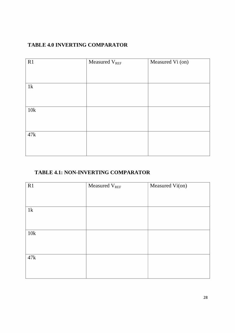
TABLE 4.0 INVERTING COMPARATOR
R1 Measured VREF Measured Vi (on)
1k
10k
47k
TABLE 4.1: NON-INVERTING COMPARATOR
R1 Measured VREF Measured Vi(on)
1k
10k
47k

29
EXPERIMENT FIVE: FIELD –EFFECT TRANSISTORS (FETS)
5.0 OBJECTIVES To examine the characteristics of a field-effect Transistor.
5.1 MATERIALS
1 FET Transistor 2N3819 or equivalent
One PSU 20V variable D.C. metered output
One 8.2kΏ resistor
One PSU 0—5V D.C. metered output
One voltmeter 0-5V D.C.
One voltmeter 0-20V D.C.
One milliammeter 0-10mA D.C.
5.2 PREPARATION The field effect transistor (FET) is a three – terminal semiconductor device having
characteristics similar to that of a pentode vacuum tube. Unlike the bipolar
Transistor, the FET is a voltage operated device (i.e. instead of being biased by
current, the FET is biased by a voltage. There are two kinds of field –effect
devices: The Junction FET (JFET) and the metal –oxide semi-conductor FET
(MOSFET). The FET has an extremely high input resistance and has no offset
voltage when used as a switch (or chopp)

30
Fig. 5.0: JFET Characteristics Circuit
5.3 PROCEDURE: Connect the circuit in fig 5.0 Ensure the power supply units (psu) control is set to
minimum. With the values of Vgs = 0, switch on the power and note VDS and ID;
Increase Vgs in steps of -1V until -4V is reached noting ID for VDS = 1, 2, 3,4, 8V
and 12V for each increment of Vgs. Tabulate your values.
Now set VDS to +1V and repeat the full set of readings as above. Finally take more
readings for VDS = + 2V, 3V, 5V, 10V and 12V.
Using The Table Of Values Obtained Above
STEP 1: Plot a graph of ID against VGS (called Transistor characteristics).
Q12SK117
50%
2.5kOhmKey = a
R1 50%
5kOhmKey = a
R2
50%
500OhmKey = a
R3
XMM1
XMM2
XMM3
V15V VDD
1.5V
VGS
VDS
ID

31
STEP 2: Plot ID against VDS (called drain characteristics).
STEP 5: Locate the knee on the forward drain characteristics VDS max and plot
log ID Versus log 10VDS max and comment on the slope. Comment on
the shape of your graphs.

32
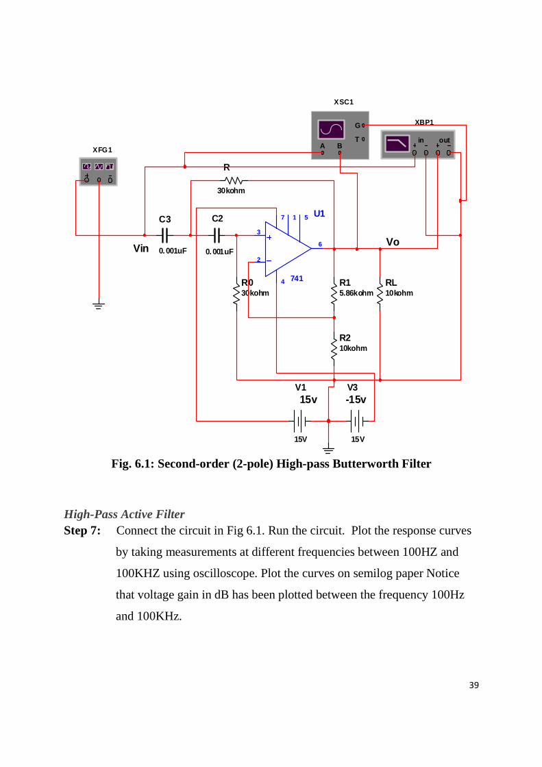
EXPERIMENT SIX: ACTIVE LOW- PASS AND HIGH – PASS FI LTERS
6.0 OBJECTIVES
1. Plot the gain-frequency response and determine the cut-off frequency of a
second-order (two-pole) low-pass active filter.
2. Plot the gain-frequency response and determine the cut-off frequency of a
second-order (two-pole) high pass active filter.
3. Determine the roll-off in dB per decade for a second-order (two-pole)
filter.
4. Plot the phase-frequency response of a second (two-pole) filter.
6.1 MATERIALS
One function generator
One dual-trace oscilloscope
One LM741 op-amp
Capacitors: two .001 µF, one pF
Resistors: one 1 kΏ, one 5.86kΏ, two 10 kΏ, two 30 Kώ
6.2 PREPARATION
In electronic communication system, it is often necessary to separate a specific
range of frequencies from the total frequency spectrum. This is normally
accomplished with filters. A filter is a circuit that passes a specific range of
frequencies while rejecting other frequencies. Active filters use active devices

33
such as op-amps combined with passive elements. Active filters have several
advantages over passive filters. The passive elements provide frequency selectivity
and active device provide voltage gain, high input impedance, and low output
impedance. The voltage gain reduces attenuation of the signal by the filter, the high
input impedance prevents excessive loading of the source, and the low output
impedance prevents the filter from being affected by the load. Active filters are
also easy to adjust over a wide frequency range without altering the required
response. The weakness of the active filters is the upper-frequency limit due to the
limited open-loop bandwidth (funity) of op-amps. The filter cut-off frequency cannot
exceed the unity-gain frequency (funity) of the op-amp. Ideally, a high-pass filter
should pass all frequencies above the cut-off frequency (fc). Because op-amps
have a limited open-loop bandwidth (unity-gain frequency, funity), high-pass active
filter have an upper-frequency limit on the high-pass response, making it appear as
a band-pass filter with a very wide bandwidth. Therefore, active filters must be
used in applications where the unity-gain frequency (funity) of the op-amp is high
enough so that it does not fall within the frequency range of the application. For
this reason, active filters are mostly used in low-frequency applications.
The four basic types of filters are low-pass, high-pass, band-pass and band-stop.
A low-pass filter is designed to pass all frequencies below the cut-off frequency
and reject all frequencies above the cut-off frequency. A high-pass filter is
designed to pass all frequencies above the cut-off frequency and rejects all the
frequencies below the cut-off frequency. A band-pass filter passes frequencies
within a band of frequencies and rejects all other frequencies outside the band. A
band-stop filter rejects all frequencies within a band of frequencies and passes all
other frequencies outside the band. A band-stop filter is often referred to as notch
filter. In this experiment, you will study active low-pass and high-pass filter.
34
The most common way to describe the frequency response characteristics of a
filter is to plot the filter voltage gain (V0/Vm) in dB as a function of frequency (f).
The frequency at which the output power gain drops to 50% of the maximum value
is called the cut-off frequency (fc). When the output power gain drops to 50%, the
voltage gain drops 3 dB (0.707 of the maximum value). When the filter dB voltage
gain is plotted as a function of frequency using straight lines to approximate the
actual frequency response, it is called a Bode plot. A Bode plot is an ideal plot of
filter frequency response because it assumes that the voltage gain remains constant
in the passband until the cut-off frequency is reached, and then drops in a straight
line. The filter network gain in dB is calculated from the actual voltage gain (A)
using the equation
AdB = 20 log A (6.1)
Where A = Vo Vin (6.2)
An ideal filter has an instantaneous roll-off at the cut-off frequency (fc), with full
signal level on one side of the cut-off frequency and no signal level on the other
side of the cut-off frequency. Although the ideal is not achievable, actual filters roll
off at 20- dB/decade or higher, depending on the type of filter. The -20-dB/decade
roll-off is obtained with one-pole filter (one R-C circuit). A two-pole filter has
two R-C circuits tuned to the same cut-off frequency and rolls off at-40 dB/decade.
Each additional pole (R-C circuit) will cause the filter to roll off an additional -
20dB/decade. In a one-pole filter, the phase between the input and the output will
change by 90 degrees over the frequency range and 45 degrees at the cut-off
frequency. In a two-pole filter, the phase will change by 180 degrees over the
frequency range and by 90 degrees at the cut-off frequency.

35
The three basic types of response characteristics that can be realized with most
active filters are Butterworth, Chebychev, and Bessel, depending on the selection
of certain filter component values. The Butterworth filter provides a flat
amplitude response in the pass-band and roll-off of -20 dB/decade/pole with a non-
linear phase response. Because of the non-linear phase response, a pulse wave
shape applied to the input of a Butterworth filter will have an overshoot on the
output. Filters with a Butterworth response are normally used in applications where
all frequencies in the pass-band must have the same gain. The Chebychev filter
provides ripple amplitude response in the pass-band and roll-off better than-20
dB/decade/pole with a less linear phase response than the Butterworth filter. Filters
with a Chebychev response are most useful when a rapid roll-off is required. The
Bessel filter provides a flat amplitude response in a pass-band and a roll-off less
than -20 dB/decade/pole with linear phase response. Because of its linear phase
response, the Bessel filter produces almost no overshoot on the output with pulse
waveforms without distorting the wave shape. Because of its maximally flat
response in the pass-band, the Butterworth is the most widely used active filter.
A second-order (two-pole) active low-pass Butterworth filter is shown in
Fig 6.0
Because it is a two-pole (two R-C circuits) low-pass filter, the output will roll-off -
40/dB per decade at frequencies above the cut-off frequency. A second-order
(two-pole) active high-pass Butterworth filter is shown in Fig 6.1. Because it is
two-pole (two R-C circuits) high-pass filter, the output will roll-off -40/dB per
decade at frequencies below the cut-off frequency. These two-pole Sallen-Key
Butterworth filters require a pass-band voltage gain of 1.586 to produce the
Butterworth response. Therefore,

36
Av = 1 + R ⁄ = 1.586 (6.3)
And
R ⁄ = 0.586 (6.4)
At the cut-off frequency of both filters, the capacitive reactance of each capacitor
(C) is equal to the resistance of each resistor (R), causing the output voltage to be
0.707 times the input voltage (-3 dB). The expected cut-off frequency (fc), based
on the circuit component values, can be calculated from
Xc = R (6.5)
= R (6.6)
Solving the fc produces the equation
=
! (6.7)

37
Fig. 6.0: Second-Order (Two-Pole) Sallen-Key Notch Filter
6.3 PROCEDURE
Low-Pass Active Filter
Step 1: Connect the circuit in Fig 6.0. Run the circuit. Plot the response curves
by taking measurements at different frequencies between 100HZ and
100KHZ using oscilloscope. Plot the curves on semilog paper Notice
that voltage gain in dB has been plotted between the frequency 100Hz
and 100KHz.
Question 6.0
a. Is the frequency responses curve that of a low-pass filter? Explain why.
Step 2 Calculate the actual voltage Gain (A) from the measured Db gain
R
54kohm
C1
0.05uF
RL10kohm
XFG1outin
XBP1
U1
741
3
2
4
7
6
51
A BT
G
XSC1
V1
15V
V3
15V
15v -15v
VinVo
R22
27kohm
C2
0.05uF
R23
54kohm
R2
10kohm
R113kohm
2C0.1uF
38
Step 3 Based on the circuit component values in fig 6.0, calculate the
Expected voltage gain (A) on the flat part of the curve for the low-pass
Butterworth filter
Question 6.1:
a. How did the measured voltage gain in step 2 compare with the Calculated
voltage gain in step 3?
Step 4: Record the decibel gain and the frequency (cut-off frequency, fc) on the
curve plot.
Step 5: Calculate the expected cut-off frequency (fC) based on the circuit
component values.
Question 6.2:
a. How did the calculated value for the cut-off frequency compare with the
measured value recorded on the curve plot for the two-pole low-pass active
filter?
Step 6: Record the dB gain frequency (f2) on the curve plot.
Questions 6.3:
a. Approximately how much did the dB gain decrease for a one-decade
increase in frequency? Was this what you expected for a two-pole filter?
39
Fig. 6.1: Second-order (2-pole) High-pass Butterworth Filter
High-Pass Active Filter Step 7: Connect the circuit in Fig 6.1. Run the circuit. Plot the response curves
by taking measurements at different frequencies between 100HZ and
100KHZ using oscilloscope. Plot the curves on semilog paper Notice
that voltage gain in dB has been plotted between the frequency 100Hz
and 100KHz.
R15.86kohm
R210kohm
RL10kohm
XFG1outin
XBP1
U1
741
3
2
4
7
6
51
A BT
G
XSC1
V1
15V
V3
15V
15v -15v
Vin Vo
C3
0.001uF
R030kohm
C2
0.001uF
R
30kohm

40
Question 6.4:
Is the frequency response curve that of a high-pass filter? Explain why.
Step 8: Calculate the actual voltage gain (A) from the dB gain.
Step 9: Based on the circuit component values in Fig 6.1, calculate the
expected voltage gain (A) on the flat part of the curve for the high-
pass Butterworth filter
Question 6.5:
a. How did the measured voltage gain in Step 8 compare with the calculated
voltage gain in Step 9?
Step 10: Record the dB gain and the frequency (cut-off frequency, fc) on the
curve plot.
Step 11: Calculate the expected cut-off frequency (fc) based on the circuit
component values.
Question 6.6:
a. How did the calculated value of the cut-off frequency compare with the
measured value recorded on the curve plot for the two-pole high-pass active
filter?
Step 12: Record the dB gain and frequency (f2) on the curve plot
Question 6.7:
a. Approximately how much did the dB gain decreases for a one-decade
decrease in frequency? Was this what you expected for a two-pole filter?

41
EXPERIMENT SEVEN: ACTIVE BAND PASS AND BAND STOP
FILTERS
7.0 OBJECTIVES
1. Plot the gain-frequency response curve and determine the centre frequency
for an active band-pass filter.
2. Determine the quality factor (Q) and bandwidth of an active band-pass
filter.
3. Plot the phase shift between the input and output for a two-pole active band-
pass filter.
4. Plot the gain-frequency response curve and determine the centre frequency
for an active band-stop (notch) filter.
5. Determine the quality factor (Q) and bandwidth of an active notch filter.
7.1 MATERIALS
One function generator
One oscilloscope
Two LM741 op-amps
Capacitors: two 0.01 µF, two 0.05 µF, and 0.1 µF
Resistors one 1 k Ω, two 10 k Ω, one 13 k Ω, one 27 k Ω, two 54 k Ω, and
One 100 k Ω

42
7.2 PREPARATION
In electronic communications systems, it is often necessary to separate a specific
range of frequencies from the total frequency spectrum. This is normally
accomplished with filters. A filter is a circuit that passes a specific range of
frequencies while rejecting other frequencies. Active filters use active devices
such as op-amps combined with passive elements. Active filters have several
advantages over passive filters. The passive elements provide frequency selectivity
and active device provide voltage gain, high input impedance, and low output
impedance. The voltage gain reduces attenuation of the signal by the filter, the high
input impedance prevents excessive loading of the source, and the low output
impedance prevents the filter from being affected by the load. Active filters are
also easy to adjust over a wide frequency range without altering the required
response. The weakness of the active filters is the upper-frequency limit due to the
limited open-loop bandwidth (funity) of op-amps. The filter cut-off frequency cannot
exceed the unity-gain frequency (funity) of the op-amp. Therefore, active filters must
be used in applications where the unity-gain frequency (funity) of the op-amp is high
enough so that it does not fall within the frequency range of the application. For
this reason, active filters are mostly used in low-frequency applications
A band-pass filter passes all the frequencies lying within a band of frequencies
and rejects all other frequencies outside the band. The low-cut-off frequency (fc1)
and the high-cut-off frequency (fc2) on the gain-frequency plot are the frequencies
where the voltage gain has dropped by dB (0.707) from the maximum gain. A
band-stop filter rejects a band of frequencies and passes all other frequencies
outside the band and the high-cut-off frequency (fc2) on the gain-frequency plot are

43
the frequencies where the voltage gain has dropped by 3 dB (0.707) from the pass-
band dB gain.
The bandwidth (BW) of a band-pass or a band-stop filter is the difference between
the high-cut-off frequency and the low cut-off frequency. Therefore,
BW = f# - f$ (7.1)
The centre frequency (f0) of a band-pass or band-stop filter is the geometric mean
of the low-cut-off frequency (fc1) and the high-cut-off frequency (fc2). Therefore,
f%= &f$f# (7.2)
The quality factor (Q) of a band-pass or a band-stop filter is the ratio of the centre
frequency (fo) and the bandwidth (BW), and is an indication of the selectivity of
the filter. Therefore,
Q = '() (7.3)
A higher value of Q means a narrower bandwidth and a more selective filter. A
filter with a Q less than one is considered to be a wide-band filter with a Q greater
than ten is considered to be a narrow-band filter.
One way to implement a band-pass filter is to cascade a low-pass and a high-pass
filter. As long as the cut-off frequencies are sufficiently separated, the low-pass
filter cut off frequency will determine the low-cut-off frequency of the band-pass
filter and the high-pass filter cut-off frequency will determine the high-cut-off
frequency of the band-pass filter. Normally this arrangement is used for a wide-
band filter (Q<1) because the cut-off frequencies need to be sufficiently separated.

44
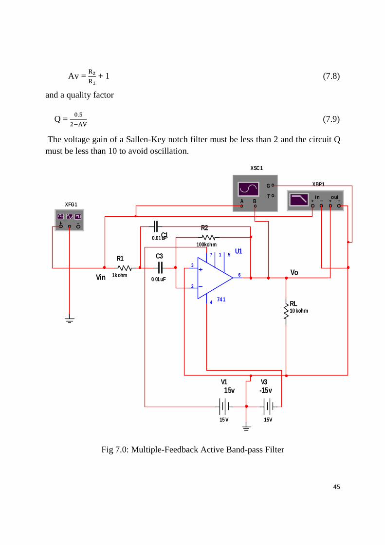
A multiple-feedback active band-pass filter is shown in Fig 7.0. Components R1
and C1 determine the low-cut-off frequency, and R2 and C2 determine the high-cut-
off frequency. The centre frequency (fo) can be calculated from the component
values using the equation
*=
&!$!#$# =
&!$!# (7.4)
Where C = C1 = C2.
The voltage gain (Av) at the centre frequency is calculated from
Av = !#!$ (7.5)
And the quality factor (Q) is calculated
Q = 0.5 + ,#,$ (7.6)
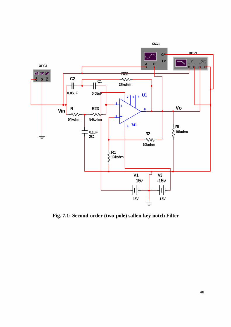
Fig 7.0 shows a second-order (two-pole) Sallen-Key notch filter. The expected
centre frequency (f0), can be calculated from
* =
! (7.7)
At this frequency (fo), the feedback signal returns with the correct amplitude and
phase to attenuate the input. This causes the output to be attenuated at the centre
frequency.
The notch filter in Fig 7.1 has a pass-band voltage gain
45
Av = ,#,$ + 1 (7.8)
and a quality factor
Q = %..
/0 (7.9)
The voltage gain of a Sallen-Key notch filter must be less than 2 and the circuit Q must be less than 10 to avoid oscillation.
Fig 7.0: Multiple-Feedback Active Band-pass Filter
R1
1kohm
C10.01uF
RL10 kohm
XFG1outi n
XBP1
U1
74 1
3
2
4
7
6
51
A BT
G
XSC1
V1
15 V
V3
15V
15v -15v
VinVo
C3
0. 01uF
R2
100kohm

46
7.3 PROCEDURE
Active Band –Pass Filter
Step 1: Connect the circuit in Fig 7.0.
Step 2: Run the circuit. Plot the response curves by taking measurements at
different frequencies between 100HZ and 10KHZ using oscilloscope.
Plot the curves on semilog paper Notice that voltage gain in dB has been
plotted between the frequency 100Hz and 10KHz.
Question 7.0:
a. Is the frequency response curves that of a band-pass filter? Explain why.
Step 3: Based on the dB voltage gain at the centre frequency, calculate the actual
voltage gain (Av)
Step 4: Based on the circuit component values, calculate the expected voltage
gain (Av) at the centre frequency (fo).
Question 7.1:
a. How did the measured voltage gain at the centre frequency compare with
voltage gain calculated from the circuit values?
Step 5: Record the frequency (low-cut-off frequency, fc1) on the curve plot.
Record the frequency (high-cut-off frequency, fc2) on the curve plot.
Step 6: Based on the measured values of fc1 and fc2, calculate the bandwidth (BW)
of the band-pass filter.
47
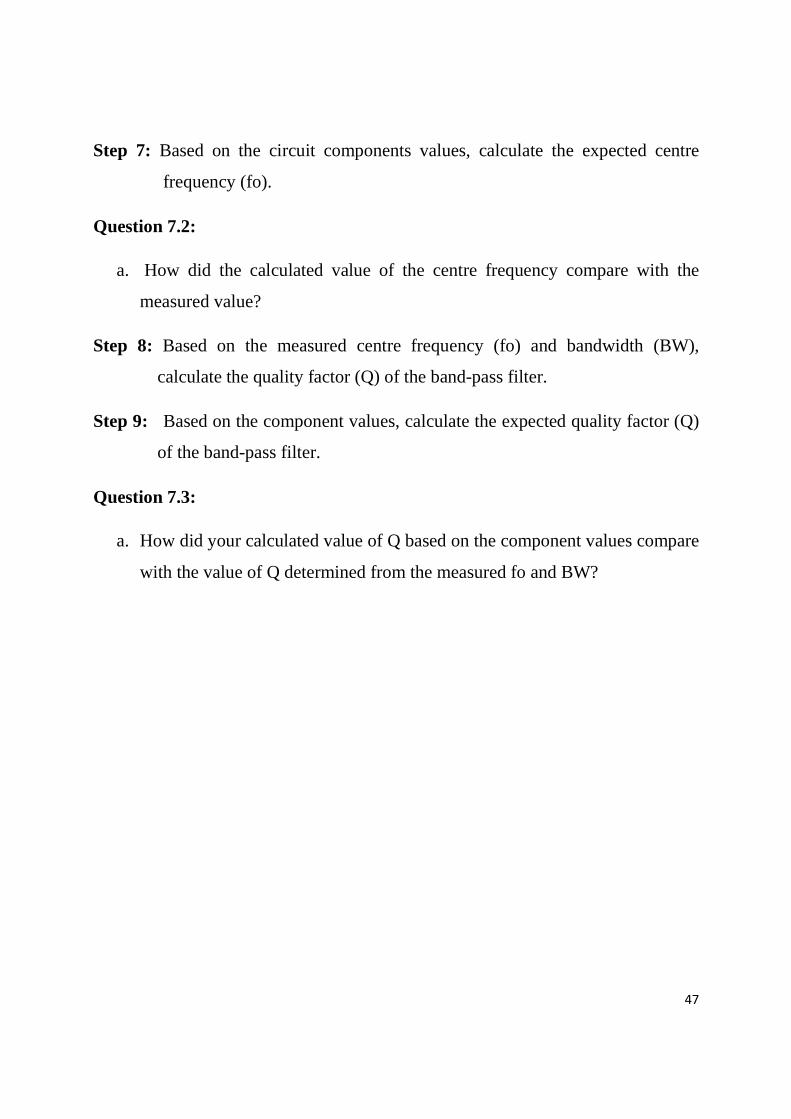
Step 7: Based on the circuit components values, calculate the expected centre
frequency (fo).
Question 7.2:
a. How did the calculated value of the centre frequency compare with the
measured value?
Step 8: Based on the measured centre frequency (fo) and bandwidth (BW),
calculate the quality factor (Q) of the band-pass filter.
Step 9: Based on the component values, calculate the expected quality factor (Q)
of the band-pass filter.
Question 7.3:
a. How did your calculated value of Q based on the component values compare
with the value of Q determined from the measured fo and BW?
48
Fig. 7.1: Second-order (two-pole) sallen-key notch Filter
R
54kohm
C1
0.05uF
RL10kohm
XFG1outin
XBP1
U1
741
3
2
4
7
6
51
A BT
G
XSC1
V1
15V
V3
15V
15v -15v
Vin Vo
R22
27kohmC2
0.05uF
R23
54kohm
R2
10kohm
R113kohm
2C0.1uF
49
EXPERIMENT EIGHT: PASSIVE LOW- PASS AND HIGH –PASS FILTERS.
8.0 OBJECTIVES
1. Plot the gain-frequency response of a first order (one-pole) R-C low pass filter.
2. Determine the cut-off frequency and roll–off of an R-C first order (one-pole)
low pass filter.
3. Plot the phase frequency response of a first order (one-pole) low pass filter.
4. Determine how the value of Rand C affects the cut off frequency of an R-C low
pass filter.
5. Plot the gain-frequency response of a first order (one-pole) R-C high pass filter.
6. Determine the cut off frequency and roll-off of a first order (one-pole) R-C high-
pass filter.
7. Plot the phase-frequency response of a first order (one-pole) high pass filter.
8. Determine how the value of R and C affects the cut off frequency of an R-C
high –pass filter.
8.1 MATERIALS
One function generator
One dual-trace oscilloscope
Capacitors: .02µf, .04µf

50
Resistor: 1k, 2k
8.2 PREPARATION
In electronics communications system, it is often necessary to separate a specific
range of frequencies types of filter from the total frequency spectrum. This is
normally accomplished with filters. A filter is a circuit that passes a specific range
of frequencies while rejecting other frequencies .A passive filter consists of passive
circuit elements such as capacitors, inductors, and resistors. There are four basic
types of filter, low-pass, high-pass, band-pass, and band-stop. A low- pass filter is
designed to pass all frequencies below the cut-off frequency and reject all
frequencies above the cut-off frequency. A high-pass all frequencies above the cut-
off frequency and reject all frequencies below the cut-off frequency. A band-pass
filter passes all frequencies within a band of frequencies and rejects all other
frequencies outside the band. A band stop filter rejects all frequencies within a
band of frequencies and passes all other frequencies outside the band. A band stop
filter is often referred to as a notch filter. In this experiment, you will study low
pass and high pass filters.
The most common way to describe the frequency response characteristics of a
filter is to plot the filter voltage gain (VO/V I) in dB as a function of frequency (f).
The frequency at which the output gain drops to 50% of the maximum value is
called the cut off frequency (FC). When the out put power gain drops to 50 %, the
voltage gain drops3dB (0.707 of the maximum value). When the filter dB voltage
gain is plotted as a function frequency on a semi log graph using straight lines to
approximate the action frequency response, it is called a Bode plot. A Bode plot is
an ideal plot of filter frequency response because it assumes that voltage gain
remains constant in the pass-band until the cut off frequency is reached and then

51
drops in a straight line. The filter network voltage gain in dB is calculated from the
actual voltage gain (A) using the equation
A(db) = 20logA (8.1)
Where A = 01023 (8.2)
A low pass RC filter is shown in fig 8.0 At frequencies well below the cut off
frequency, the capacitive reactance of a capacitor C is much higher than the
resistance of the resistor R, causing the output voltage to be practically equal to the
input voltage (A=1) and constant with variations in frequency. At frequencies well
above the cut off frequencies, the capacitive reactance of capacitor C is much
lower than the resistance of resistor R and decreases with an increase in frequency,
causing the output voltage to decrease 20 dB
Per decade, increase in frequency. At the cut off frequency, the capacitive
reactance of capacitor C is equal to the resistance of the resistor R, causing the out
voltage to be 0.707 times the input voltage (-3dB). The expected cut off frequency
(fc) of the low pass filter in figure 19.0, based on the circuit component values, can
be calculated from
Xc = R (8.3)
45 = R (8.4)
Solving for fc produces the equation
* =
! (8.5)
A high pass RC filter is shown in fig 19.1. At frequencies well above the cut off
frequency, the capacitive reactance of capacitor C is much lower than the

52
resistance of resistor R, causing the output voltage to be practically equal to the
input voltage A= 1 and constant with variations in frequency. At frequencies
well below the cut-off frequency, the capacitive reactance of capacitor C is much
higher than the resistance of resistor R and increases with a decrease in frequency,
causing the output voltage to decrease 20 dB per decade decrease in frequency. At
the cut-off frequency, the capacitive reactance of capacitor C is equal to the resistor
R, causing the voltage to be 0.707 times the input voltage -3 Db). The expected
cut-off frequency fc of the high-pass filter in fig 8.2, based on the circuit
component values, can be calculated from
* =
! (8.6)
When the frequency at the input of a low-pass filter increases above the cut-off
frequency, the filter output voltage drops at a constant rate. When the frequency at
the input of a high- pass filter decreases below the cut-off frequency, the filter
output voltage also drops at a constant rate. The constant drop in filter output
voltage per decade increases ×10, or decrease ÷10, in frequency is called roll-
off. An ideal low- pass or high-pass filter would have an instantaneous drop at the
cut-off frequency [fc], with full signal level on one side of the cut-off frequency
and no signal level on the other side of the cut-off frequency. Although the ideal is
not achievable, actual filters roll off at -20dB/decade per pole [R- C Circuit]. A
one-pole filter has one R-C circuit tuned to the cut-off frequency and rolls off at -
20dB/decade. A two-pole has two R-C circuits tuned to the same cut-off frequency
and rolls at -40dB/decade. Each additional pole [R-C circuit] will cause the filter to
roll an additional -20dB/decade. Therefore, an R-C filter with more poles [R-C
circuits] more closely approaches an ideal filter.

53
In a one- pole filter, as shown in fig 8.0 and 8.1, the phase [ø] between the input
and the output will change by 90 degrees over the frequency range and be 45
degrees at the cut-off frequency. In a two- pole filter, the phase [ø] will change by
180 degrees over the frequency range and be 90 degrees at the cut-off frequency.
Fig. 8.0: Low-pass R-C Filter
R1
1kohm
C10.02uF
outin
XBP1
XFG1
54
Fig. 8.1: High-pass R-C Filter
8.3 PROCEDURE
Low-pass filter
Step 1: Connect the circuit in Fig 8.0. Make sure that the following Bode plotter
settings are selected: Magnitude, Vertical (Log, F = 0dB, I= -40dB),
Horizontal (Log, F = 1 MHz, I = 100Hz).
Step 2: Run the circuit. Plot the response curves by taking measurements at
different frequencies between 100HZ and 1MHZ using oscilloscope. Plot
the curves on semilog paper Notice that voltage gain in dB has been
plotted between the frequencies of 100Hz and 1MHz.
Question 8.0:
a. Is the frequency response curves that of a low-pass filter? Explain why.
outin
XBP1
XFG1
C2
0. 02uF
R21kohm
55
Step 3: Calculate the actual voltage gain [A] from the dB voltage gain [AdB].
Questions 8.1:
a. Was the voltage gain on the flat part of the frequency response curve what
you expected for the circuit in Fig 8.0? Explain why.
Step 4: Calculate the expected cut-off frequency (fc) based on the circuit
component values in Fig 8.0.
Questions 8.2:
a. How did the calculated value for the cut-off frequency compare with the
measured value recorded on the curve plot? How much did the dB gain
decrease for a one-decade increase (x 10) in frequency? Was it what you
expected for a single-pole (single R-C) low pass filter?
Step 5: Connect the circuit in fig 8.1. Plot the response curves by taking
measurements at different frequencies between 100HZ and 1MHZ using
oscilloscope. Plot the curves on semilog paper Notice that voltage gain in
dB has been plotted between the frequencies of 100Hz and 1MHz.
Question 8.3:
a. Is the frequency response curves that of a high-pass filter? Explain why.
Step 6: Calculate the actual voltage gain [A] from the dB voltage gain [AdB].
Step 7: Calculate the expected cut-off frequency (fc) based on the circuit
component values in Fig 8.1
Questions 8.3:

56
a. How did the calculated value for the cut-off frequency compare with the
measured value recorded on the curve plot? How much did the dB gain
decrease for a one-decade increase (x 10) in frequency? Was it what you
expected for a single-pole (single R-C) high- pass filter?

57
EXPERIMENT NINE: PASSIVE BAND-PASS AND BAND-STOP FI LTERS
9.0 OBJECTIVES
1. Plot the gain-frequency response of an L-C series resonant and an L-C parallel
resonant band-pass filter.
2. Determine the centre frequency and the bandwidth of the L-C band –pass
filters.
3. Determine how the circuit resistance affects the bandwidth of an L-C band-
pass filter.
4. Plot the gain-frequency response of an L-C series resonant and an L-C parallel
resonant band-stop [notch] filter.
5. Determine the centre frequency and bandwidth of the L-c band-stop filters.
6. Determine how the circuit resistance affects the bandwidth of an L-C band-
stop filter.
9.1 MATERIALS
One function generator
One dual-trace oscilloscope
Capacitors: one 0.1µF, one 0.25µF
Inductors: one 50mH, one 100mH
Resistors: 100Ω, 200 Ω, 2k, 4k, 5k, 200k
58
9.2 PREPARATION
In electronic communications systems, it is often necessary to separate a specific
range of frequencies from the total frequency spectrum. This is normally
accomplished with filters. A Filter is a circuit that passes a specific range of
frequencies while rejecting other frequencies. A passive filter consists of passive
circuit elements, such as capacitors, inductors, and resistors. There are four basic
types of filters; low-pass, high-pass filter band-pass and band-stop. A low-pass
filter is designed to pass all frequencies below the cut-off frequency and reject all
frequencies above the cut-off frequency. A high-pass filter is designed to pass all
frequencies above the cut-off frequency and rejects all frequencies below the cut-
off frequency. A band-pass filter passes all frequencies within a band of
frequencies and rejects all other frequencies outside the band. A band-stop filter
rejects all frequencies within a band of frequencies and passes all other frequencies
outside the band. A band-stop filter is often referred to as a notch filter. In this
experiment, you will study band-pass and band-stop [notch] filters. The most
common way to describe the frequency response characteristics of a filter is to plot
the filter voltage gain [Vo/Vin] in dB as function of frequency [f]. The frequency
at which the output power gain drops to 50%, the maximum value is called the cut-
off frequency [fc]. When the output power drops 50%, the voltage gain drops 3db
[0.707 of the maximum value]. When the filter dB voltage gain is plotted as a
function of frequency on a semi log graph using straight lines to approximate the
actual frequency response, it is called a Bode plot. A Bode plot is an ideal plot of
frequency response because it assumes that the voltage gain remains constant in
the pass band until the cut-off frequency is reached, and then drops in a straight
lime. The filter network voltage gain in db calculated from the actual voltage gain
[A] using the equation
59
A dB=20 log A (9.1)
Where A = 01023 (9.2)
An L-C series resonant band-pass filter is shown in fig 9.0. The impedance of the
series L-C circuit is lowest at the frequency and increases on both sides of the
resonant frequency. This will cause the output voltage to be highest at the resonant
frequency and decrease on both sides of the resonant frequency. An L-C parallel
resonant band-pass filter is shown in figure 9.1. The impedance of the parallel L-C
circuit is highest at the resonant frequency and decreases on both sides of the
resonant frequency. This will also cause the output voltage to be highest at the
resonant frequency and decrease on both sides the resonant frequency.
An L-C series resonant band-stop [notch] filter is shown in fig 9.2. The impedance
of the series L-C circuit is lowest at the resonant frequency and increases on both
sides of the resonant frequency. This will cause the output voltage to be lowest at
the resonant frequency and increase on both sides of the resonant frequency. An L-
C parallel resonant band-stop [notch] filter is shown in fig 9.3. The impedance of
the parallel L-C circuit is highest at the resonant frequency and decreases on both
sides of the resonant frequency. This will also cause the output voltage to be lowest
at the resonant frequency and increase on both sides of the resonant frequency.
The centre frequency [fo] for the L-C Series resonant and the L-C parallel resonant
band-pass and band-stop [[notch] filter is equal to the resonant frequency of the L-
C circuit, which can be calculated from
f6 =
√8 (9.3)
For an L-C parallel resonant filter, the equation is accurate only for a high Q
inductor coil [QL≥10], where QL is calculated
60
Q8 = :;,< (9.4)
In addition, XL is the inductive reactance at the resonant frequency [centre
frequency, fo] and Rw is the inductor coil resistance.
In the band-pass and band-stop [notch] filters, the low-cut-off frequency [fc1]
and the high-cut-off frequency [fc2] on the gain-frequency plot are the
frequencies where the voltage gain has dropped 2dB[0.707] from the highest db
gain. The filter bandwidth [BW] is the difference between the high- cut-off
frequency [fc2] and the low-cut-off frequency [fc1]. Therefore
BW = fc2- fc1. (9.5)
The centre frequency [fo] is the geometric mean of the low-cut-off frequency
and the high-cut-off frequency. Therefore,
* = & (9.6)
The quality factor [Q] of the band-pass and band-stop [notch] is the ratio of the
centre frequency [fo] and the bandwidth [BW], and it is the indication of the
selectivity of the filter. Therefore,
Q = 1() (9.7)
A higher value of Q means a narrower bandwidth and a more selective filter.
The quality factor [Qs] of a series resonant filter is determine by first
calculating the inductive reactance [XL] of the inductor at the resonant
frequency [centre frequency, fo], and then dividing the total parallel resistance

61
[Rp] by the inductive reactance [XL] by the total series resistance (RT).
Therefore,
Qs = :;,= (9.8)
Where L 0X = 2 f Lπ (9.9)
The quality factor (Qp) of a parallel resonant filter is determined by first
calculating the inductive reactance (XL) of the inductor at the resonant
frequency (centre frequency, f0), and then dividing the total parallel resistance
(Rp) by the inductive reactance (XL)
Qp = !'>? (9.10)
Because the inductor wire resistance [Rw] is in series with inductor L, the circuit
in fig 9.1 and 9.3 are exactly parallel resonant circuits. In order to make them be
true parallel resonant circuits, the series combination of inductance [L] and
resistance [Rw] must first be converted into an equivalent parallel network with
resistance Req in parallel with inductance L. in fig 9.1, the parallel equivalent
resistance [Req] will also be in parallel with resistor R and resistor, Rs, making
the total resistance of the parallel resonant circuit [Rp] equal to the parallel
equivalent of resistors R, Rs, and Req. therefore, Rp can be solved from
,@ =
, +
,A +
,BC (9.11)
In fig 9.3, the parallel equivalent resistance [Req] will be in parallel with resistor,
making the total resistance of the parallel resonant circuit [Rp] equal to the
parallel equivalent of resistors R and Req. therefore, Rp can be solved from
62
RD = E,FE,BCF,G,BC (9.12)
The equation for converting resistance Rw to the equivalent parallel
Resistance [Req] is
2LReq = Rw [Q + 1] (9.13)
The parallel equivalent inductance [Leq] is calculated from
2 2L LLeq = L [Q + 1] Q (9.14)
This equivalent inductance can be considered equal to the original inductance [L]
for a high Q coil [QL≥10].
Fig. 9.0: L-C Parallel Resonant Band-stop (Notch) Filter
Rw
20ohm
R4kohm
L
100mH
C 0.25uF
XFG1outin
XBP1
Vin
Vo

63
Fig. 20.1: L-C Parallel Resonant Band-pass Filter
Fig. 9.2: L-C Series Resonant Band-Stop (Notch) Filter
Rw20ohm
R200kohm
L
100mH
XFG1
outin
XBP1
Vin
Vo
C2
0.25uF
Rs
5kohm
Rw20ohm
L
100mH
XFG1
outin
XBP1
Vin
Vo
C
0.25uF
Rs
100ohm
64
Fig. 9.3: L-C Parallel Resonant Band-Stop (Notch) Filter
9.3 PROCEDURE
Band-pass filters
Step 1: Connect the circuit in Fig 9.0. Make sure that the following Bode plotter
settings are selected: Magnitude, Vertical (Log, F = 0dB, I= -20dB),
Horizontal (Log, F = 2 KHz, I = 500Hz).
Step 2: Run the circuit. Plot the response curves by taking measurements at
different frequencies between 500HZ and 2KHZ using oscilloscope. Plot
Rw
20ohm
R4kohm
L
100mH
C 0.25uF
XFG1outin
XBP1
Vin
Vo

65
the curves on semilog paper Notice that voltage gain in dB has been
plotted between the frequency 500Hz and 2KHz
Question 9.0:
a. Is the frequency response curves that of a band-pass filter? Explain why.
Step 3: Based on the dB voltage gain, calculate the actual voltage gain [A] of the
series resonant band-pass filter at the centre frequency.
Step 4: Record the approximate frequency [low-cut-off frequency, fc1] on the
curve plot. Record the approximate frequency [high-cut-off frequency,
fc2] on the curve plot.
Step 5: Based on the values of fc1 and fc2 measured on the curve plot, determine
the bandwidth [BW] of the series resonant band-pass filter.
Step 6: Based on the circuit component values in fig 9.0, calculate the expected
centre frequency [fo] of the series resonant band-pass filter.
Question 9.1:
a. How did the calculated values of the centre frequency [fo] based on the
circuit component values compare with the measured value recorded on the
curve plot?
Step 7: Based on the values of fc1 and fc2; calculate the centre frequency [fo].
Question 9.2:
a. How did the calculated value of the centre frequency [fc] based on fc1 and
fc2 compare with the measured value on the curve plot?

66
Step 8: Based on the component values, calculate the quality factor [Qs] of the
series resonant band-pass filter.
Step 9: Based on the circuit quality factor [Qs] and the centre frequency [fo],
calculate the expected bandwidth BW of the series resonant band-pass
filter.
Question 9.3:
a. How did the expected bandwidth calculated from the value of centre
frequency compare with the bandwidth measured on the curve plot?
Step 10: Change the resistance of R to 200ohms. Run the circuit again. Measure
the centre frequency [fo] and the bandwidth [BW] from the curve plot
and record the values.
Fo = BW=
Questions 9.4:
a. What effect did changing the resistance of R have on the centre frequency of
the series resonant band-pass filter? What effect did changing the resistance
of R have on the bandwidth of the series resonant band-pass filter? Explain.
Step 11: Change the capacitance of C to 0.1µF. Run the circuit again. Measure the
centre frequency [fo] and the bandwidth [BW] on the curve plot and
record the values.
Fo = BW=
Questions 9.5:

67
a. What effect did changing the capacitance of C have on the centre frequency
of the series resonant band-pass filter? What effect did changing the
capacitance of C have on the bandwidth of the series resonant band-pass
filter? Explain.
Change the inductance of L to 50 mH. Run the circuit again. Measure the
centre frequency [fo] the bandwidth [BW] on the curve plot and record the
values.
Fo= BW=
Questions 9.6:
a. What effect did changing the inductance of L have on the centre frequency
of the series resonant band- pass filter? What effect did changing the
inductance of L have on the bandwidth of the series resonant band-pass
filter? Explain.
Step 13: Connect the circuit in Fig 9.1 Run the circuit. Plot the response curves
by taking measurements at different frequencies between 500HZ and
2KHZ using oscilloscope. Plot the curves on semilog paper Notice that
voltage gain in dB has been plotted between the frequency 500Hz and
2KHz.
Question 9.7:
Is the frequency response curves that of a band-pass filter? Explain why.
Step 14: Record the centre frequency [fo] and the voltage gain in dB on the curve
plot.

68
Step 15: Based on the dB voltage gain, calculate the actual voltage gain [A] of the
parallel resonant band-pass filter at the centre frequency.
Step 16: Record the approximate frequency [low-cut-off frequency, fc1] on the
curve plot. Record the approximate frequency [high-cut-off frequency,
fc2] on the curve plot.
Step 17: Based on the circuit component values in fig 9.1, calculate the expected
centre frequency [fo] of the parallel resonant band-pass filter.
Question 9.8:
a. How did the calculate value of the centre frequency [fo] based on the circuit
component values compare with the measured value recorded on the curve
plot?
Step 18: Based on the values of fc1 and fc3, calculate the centre frequency [fo].
Question 9.9:
a. How did the calculate value of the centre frequency [fo] based on fc1 and fc2
compare with the measured value on the curve plot?
Step 19: Based on the value of L and Rw; calculate the quality factor [QL] of the
inductor.
Step 20: Based on the quality factor [QL] of the inductor, calculate the equivalent
parallel inductor resistance [Req] across the tank circuit.
Step 21: Based on the value of Req, Rs, and R, calculate the total parallel
resistance [Rp] across the tank circuit.

69
Step 22: Based on the value of Rp; calculate the quality factor [Qp] of the parallel
resonant band-pass filter.
Step 23: Based on the filter quality factor [Qp] the centre frequency [fo], calculate
the expected bandwidth [BW] of the parallel resonant band-pass filter.
Question 9.10:
a. How did the expected bandwidth calculated from the value of Qp and the
centre frequency compare with the bandwidth measured on the curve plot?
Step 24: Change the resistance of R to 5kohm. Run the circuit again. Measure the
centre frequency [fo] and the bandwidth [BW] from the curve plot and
record the values.
Fo= BW=
Questions 9.11:
a. what effect did changing the resistance of R have on the centre frequency of
the parallel resonant band-pass filter? What effect did changing the
resistance of R have on the bandwidth of the parallel band-pass filter?
Explain why.
Band-stop [notch] filters
Step 25: Connect the circuit in Fig 9.2. Run the circuit. Plot the response curves
by taking measurements at different frequencies between 500HZ and
2KHZ using oscilloscope. Plot the curves on semilog paper Notice that
voltage gain in dB has been plotted between the frequency 500Hz and
2KHz
70
Question 9.12:
a. Is the frequency response curves that of a band-stop [notch] filter? Explain
why.
Step 26: Record the centre frequency [fo] on the curve plot.
Step 27: Record the dB gain on the curve plot.
Step 28: Record the approximate frequency [low- cut-off frequency, fc1]
on the curve plot. Record the approximate frequency [high-cut-off
frequency, fc2] on the curve plot.
Step 29: Based on the values of fc1 and fc2; determine the bandwidth [BW] of the
series resonant band-stop filter.
Step 30: Based on the circuit component values in figure 20.2, calculate the
expected centre [fo] of the series resonant band-stop [notch] filter.
Question 9.13:
a. How did the calculated value of the centre frequency [fo] based on the
circuit component values compare with the measured value recorded on the
curve plot?
Step 31: Based on the values of fc1 and fc2; calculate the centre frequency [fo].
Question 9.14:
a. How did the calculated value of the centre frequency [fo] based on fc1 and
fc2 compare with the measured value on the curve plot?
71
Step 32: Based on the circuit component values, calculate the quality factor [Qs]
of the series resonant band-stop [notch] filter.
Step 33: Based on the circuit quality factor [Qs] and the centre frequency [fo],
calculate the expected bandwidth [BW] of the series resonant band-stop
[notch] filter.
Question 9.15:
a. How did the expected bandwidth calculated from the value of Qs and the
centre frequency compare with the bandwidth measured on the curve plot?
Step 34: Connect the circuit in file Fig 9.3. Run the circuit. Plot the response
curves by taking measurements at different frequencies between 500HZ
and 2KHz using oscilloscope. Plot the curves on semilog paper Notice
that voltage gain in dB has been plotted between the frequency 500Hz
and 2KHz.
Question 9.16:
a. Is the frequency response curves that of a band-stop [notch] filter? Explain
why.
Step 35: Record the centre frequency [fo] on the curve plot.
Step 36: Record the dB gain on the curve plot.
Step 37: Record the approximate frequency [low-cut-off frequency, fc1] on the
curve plot. Record the approximate frequency [high-cut-off frequency,
fc2] on the curve plot.

72
Step 38: Based on the values of fc1 and fc2; determine the bandwidth [BW] of the
parallel resonant band-stop [notch] filter.
Step 39 Based on the circuit component values in fig 9.3, calculate the expected
centre frequency [fo] of the parallel resonant band-stop [notch] filter.
Question 9.17:
a. How did the calculate value of the centre frequency [fo] based on the circuit
component values compare with the measured value recorded on the curve
plot?
Step 40: Based on the values of fc1 and fc2 calculate the centre frequency [fo].
Question 9.18:
a. How did the calculated value of the centre frequency [fo] based on fc1 and
fc2 compare with the measured value on the curve plot?
Step 41: Based on the value of L and Rw; calculate the quality factor [QL] of the
inductor.
Step 42: Based on the quality factor [QL] of the inductor, calculate the equivalent
parallel inductor resistance [Req] across the tank circuit.
Step 43: Based on the value of Req and R; calculate the total parallel resistance
[Rp] across the tank circuit.
Step 44: Based on the value of Rp, calculate the quality factor [Qp] of the parallel
resonant band-stop [notch] filter.
73
Step 45: Based on the filter quality factor [Qp] and the centre frequency [fo],
calculate the expected bandwidth [BW] of the parallel resonant band-stop
[notch] filter.
Question 9.19:
a. How did the expected bandwidth calculated from the value of Qp and the
centre frequency compare with the bandwidth measured on the curve lot?
Step 46: Change the resistance of R to 2kohms. Run the circuit again. Measure the
centre frequency [fo] and the bandwidth [BW] from the curve plot and
record the values.
Fo = BW=
Questions 9.20:
a. What effect did changing the resistance of R have on the centre frequency of
the parallel resonant band-stop [notch] filter? What effect did changing the
resistance of R have on the bandwidth of the parallel resonant band-stop
[notch] filter? Explain.


![LABORATÓRIO DE SISTEMAS MECATRÔNICOS E ROBÓTICA ] - LAB.pdf · Resistores - 1,0 Ω - 100k Ω 1,2 Ω - 120k Ω 1,5 Ω - 150k Ω 1,8 Ω- 180k Ω 2,2 Ω– 220k Ω 2,7 Ω– 270k](https://img.pdfslide.net/doc/110x75/5c245c1a09d3f224508c4b48/laboratorio-de-sistemas-mecatronicos-e-robotica-labpdf-resistores-.jpg)