Embed Size (px)
DESCRIPTION
Is There a Nanocrystalline Diamond Raman Peak in Nanocrystalline Diamond
Citation preview
IS THERE A "NANOCRYST ALLINE DIAMOND" RAMAN PEAK IN NANOCRYSTALLINE DIAMOND?
A. C. FERRARI and J. ROBERTSON
Department of Engineering, University of Cambridge, Cambridge, CB2 1 PZ, UK
Abstract. It is argued that the peak near 1150 em·• in the visible Raman spectra of poor quality chemical vapour deposited diamond should not be assigned to nano-crystalline diamond or other sp3 bonded phases. Its wavenumber disperses with excitation energy, its intensity decreases with increasing excitation energy, and it is always accompanied by another peak near 1450 em·•, which acts similarly. This behaviour is that expected for sp2 bonded configurations with their smaller band gap. The peaks are assigned to trans-polyacetylene segments at the grain boundaries and surfaces.
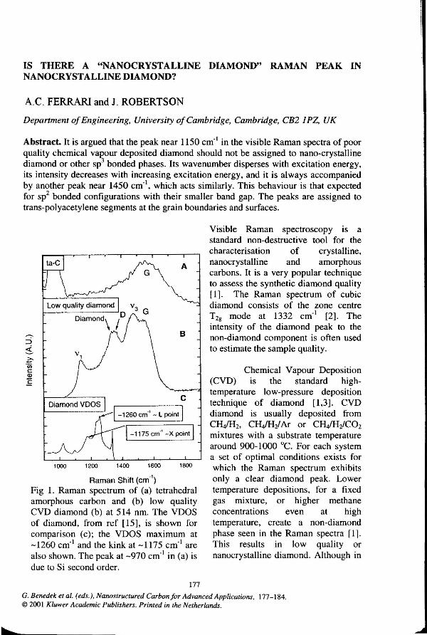
Low quality diamond
Diamond\ /D
v1
A
B
c 1-1260 em·'- L point I
1-1 t75 em·' -X point I
1000 1200 1400 1600 1800
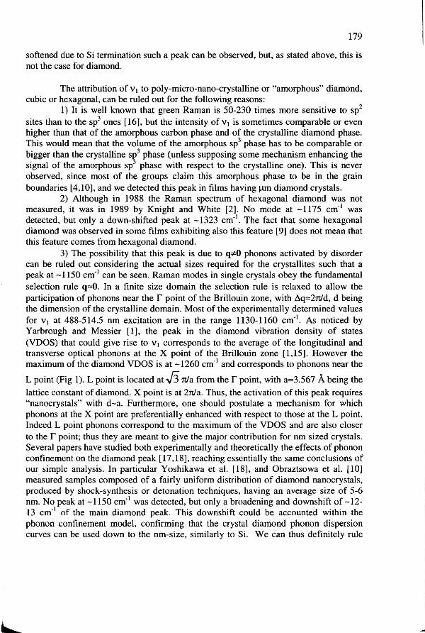
Raman Shift (em·') Fig 1. Raman spectrum of (a) tetrahedral amorphous carbon and (b) low quality CVD diamond (b) at 514 nm. The VDOS of diamond, from ref [15], is shown for comparison (c); the VDOS maximum at -1260 em·• and the kink at -1175 em·• are also shown. The peak at -970 em·• in (a) is due to Si second order.
177
Visible Raman spectroscopy is a standard non-destructive tool for the characterisation of crystalline, nanocrystalline and amorphous carbons. It is a very popular technique to assess the synthetic diamond quality [1]. The Raman spectrum of cubic diamond consists of the zone centre T2g mode at 1332 em·• [2]. The intensity of the diamond peak to the non-diamond component is often used to estimate the sample quality.
Chemical Vapour Deposition (CVD) is the standard hightemperature low-pressure deposition technique of diamond [1,3]. CVD diamond is usually deposited from CH,JH2, CHJH2/ Ar or CHJH2/C02
mixtures with a substrate temperature around 900-1000 °C. For each system a set of optimal conditions exists for which the Raman spectrum exhibits only a clear diamond peak. Lower temperature depositions, for a fixed gas mixture, or higher methane concentrations even at high temperature, create a non-diamond phase seen in the Raman spectra [1]. This results in low quality or nanocrystalline diamond. Although in
G. Benedek et al. (eds.), Narwstructured Carbon for Advanced Applications, 177-184. © 2001 Kluwer Academic Publishers. Printed in the Netherlands.
178
the past the aim was to maximise the quality of the deposit, recently production of low quality or nanocrystalline diamond is of great interest for field emission or tribology [ 4]. It is therefore important to understand the origin of the non-diamond features in the Raman spectra.
Fig 1 shows a green Raman spectrum that we measured on a diamond sample grown away from optimum conditions with a MW-plasma-CVD at 1300W, -780 °C, 180 seem H2, 17.5 seem C~, 2.5 seem C02 at 45mbar [5]. Similar spectra have been reported by a number of different groups (e.g. ref [1, 4,7-14]). A part from the tiny diamond peak, four other features are immediately recognisable around 1150, 1350, 1450, 1550 em·'. The peaks at -1350 em·' and 1550 em·' are assigned to the D and G modes of disordered or amorphous carbons. The D peak is due to rings breathing modes whilst the G peak is due to the relative motion of sp2 carbon atoms, both in rings and chains [6]. The peak at -1150 em·' is generally considered to be due to "nanocrystalline diamond" [1]. In the following we will refer to this peak as v 1 and to the peak at -1450 em·' as v3.
The origin of v1 and v3 was firstly investigated by Nemanich et a!. in their pioneering work of 1988 [7]. They proposed that v1 was due to regions of "microcrystalline or amorphous diamond". They also postulated that this should be hexagonal diamond, for which they expected the strongest mode to be at -1175 em·', with a weaker feature at -1330 em·'. For the origin of peak v3 they made 2 proposals: 1) amorphous network of four and threefold coordinated carbon atoms; 2) an impuritycarbon amorphous network, due to the presence of amorphous carbon rich SiC in the films. These hypotheses have been the basis for the interpretation of the non-diamond phase for the past years. Subsequent workers have always supported this assignment. This was largely because this wavenumber roughly corresponds to a maximum in the vibrational density of states (VDOS) of diamond [ 10,13-14].
The purpose of this paper is to critically analyse these hypotheses and their more recent slight upgrades [10]. We will show how, just relying on the published literature, we can rule out any link between v 1 and v3 and C-C sp3 vibrations. We will then present a multi-wavelength study of a typical nanocrystalline diamond sample and propose a new attribution for v1 and v3•
The attribution of v3 to a SiC related mode can be readily ruled out due to the observation of this peak for samples grown in substrates other than Si [ 12] and since its intensity does not decrease with sample thickness [12]. Some groups proposed that this peak should be due to an "sp3 bonded carbon phase" [10, 13]. However this is not possible since no C-C sp3 mode lies above -1360 em·' [15]. The alternative attribution to an amorphous network of sp2-sp3 bonds [7,12] is unlikely since such a low frequency peak is generally not observed in green Raman of amorphous carbons with any mixture of sp2 and sp3 bonds [6]. Indeed, an sp2-sf bond is polar and should have a lower Raman cross section than a sp3 -sp3 and sp -sp2 bond. Only when C-C vibrations are
179
softened due to Si termination such a peak can be observed, but, as stated above, this is not the case for diamond.
The attribution of v 1 to poly-micro-nano-crystalline or "amorphous" diamond, cubic or hexagonal, can be ruled out for the following reasons:
1) It is well known that green Raman is 50-230 times more sensitive to sp2
sites than to the sp3 ones [16], but the intensity ofv1 is sometimes comparable or even higher than that of the amorphous carbon phase and of the crystalline diamond phase. This would mean that the volume of the amorphous sp3 phase has to be comparable or bigger than the crystalline s~3 phase (unless supposing some mechanism enhancing the signal of the amorphous sp phase with respect to the crystalline one). This is never observed, since most of the groups claim this amorphous phase to be in the grain boundaries [4,10], and we detected this peak in films having J.lm diamond crystals.
2) Although in 1988 the Raman spectrum of hexagonal diamond was not measured, it was in 1989 by Knight and White [2]. No mode at -1175 em·• was detected, but only a down-shifted peak at -1323 em·•. The fact that some hexagonal diamond was observed in some films exhibiting also this feature [9] does not mean that this feature comes from hexagonal diamond.
3) The possibility that this peak is due to q;tO phonons activated by disorder can be ruled out considering the actual sizes required for the crystallites such that a peak at -1150 em·• can be seen. Raman modes in single crystals obey the fundamental selection rule q:::O. In a finite size domain the selection rule is relaxed to allow the participation of phonons near the r point of the Brillouin zone, with ilq:::21t/d, d being the dimension of the crystalline domain. Most of the experimentally determined values for v 1 at 488-514.5 nm excitation are in the range 1130-1160 em·•. As noticed by Yarbrough and Messier [1], the peak in the diamond vibration density of states (VDOS) that could give rise to v 1 corresponds to the average of the longitudinal and transverse optical phonons at the X point of the Brillouin zone [1,15]. However the maximum of the diamond VDOS is at -1260 em·• and corresponds to phonons near the
L point (Fig 1). L point is located at .J3 1t/a from the r point, with a=3.567 A being the
lattice constant of diamond. X point is at 21t/a. Thus, the activation of this peak requires "nanocrystals" with d-a. Furthermore, one should postulate a mechanism for which phonons at the X point are preferentially enhanced with respect to those at the L point. Indeed L point phonons correspond to the maximum of the VDOS and are also closer to the r point; thus they are meant to give the major contribution for nm sized crystals. Several papers have studied both experimentally and theoretically the effects of phonon confinement on the diamond peak [ 17, 18], reaching essentially the same conclusions of our simple analysis. In particular Yoshikawa et al. [18], and Obraztsowa et al. [10] measured samples composed of a fairly uniform distribution of diamond nanocrystals, produced by shock-synthesis or detonation techniques, having an average size of 5-6 nm. No peak at -1150 em·• was detected, but only a broadening and downshift of -12-13 em·• of the main diamond peak. This downshift could be accounted within the phonon confinement model, confirming that the crystal diamond phonon dispersion curves can be used down to the nm-size, similarly to Si. We can thus definitely rule
.J
r
180
out that v 1 has anything to do with poly-micro or nanocrystalline diamond. The only possibility left is that this peak stems from a atomic scale disordered sp3 network, with enough bond angle and bond length disorder to soften the VDOS of at least -100 em·• (differently from amorphous Si or Ge, where no softening is observed).
4) In 1988 tetrahedral amorphous carbon (ta-C) was not yet produced, but nowadays depositing an amorphous carbon with 85-90% sp3 is a standard procedure. In Fig 1 we show the 514.5 nm Raman spectrum of a ta-C grown by an S-bend Filtered Cathodic Vacuum arc (FCVA) [6]. No faintest peak at 1100-1200 em·• is seen, since the remaining 10-15% sp2 sites overshadow the direct contribution of the sp3 phase at this excitation wavelength. On the contrary, in low quality diamond, v 1 has a comparable intensity to the amorphous carbon phase. Thus, it is unlikely that even a 100% sp3 amorphous phase in the grain boundaries could give a signal bigger than the sp2 phase, which is also in the grain boundaries [ 10, 4]. This rules out the attribution of v1 to an amorphous sp3 phase.
If v 1 and v3 are not due to C-C sp3 vibrations they must to be due to C-C sp2,
but in a different configuration than amorphous carbon. As noted by others [ 10, 14] v 1
and v3 seem to occur always in pair, but the attribution of v3 to a C-C sp3 vibration can be straightforwardly ruled out. This again implies that v 1 cannot be due to C-C sp3
• In order to finally identify these peaks we performed a multi-wavelength investigation of
30000
25000
20000
::i ~15000
5000
Raman Shift (cm.1)
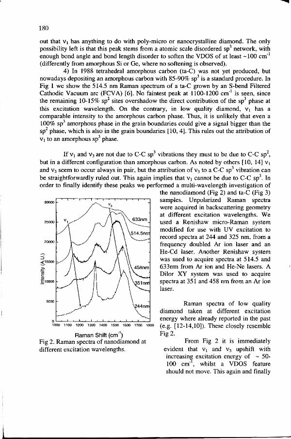
Fig 2. Raman spectra of nanodiamond at different excitation wavelengths.
the nanodiamond (Fig 2) and ta-C (Fig 3) samples. Unpolarized Raman spectra were acquired in backscattering geometry at different excitation wavelengths. We used a Renishaw micro-Raman system modified for use with UV excitation to record spectra at 244 and 325 nm, from a frequency doubled Ar ion laser and an He-Cd laser. Another Renishaw system was used to acquire spectra at 514.5 and 633nm from Ar ion and He-Ne lasers. A Dilor XY system was used to acquire spectra at 351 and 458 nm from an Ar ion laser.
Raman spectra of low quality diamond taken at different excitation energy where already reported in the past (e.g. [12-14,10]). These closely resemble Fig2.
From Fig 2 it is immediately evident that v1 and v3 upshift with increasing excitation energy of - 50-100 em·•, whilst a VDOS feature should not move. This again and finally
181
confirms that v 1 cannot be due to a C-C sp3 vibration. Furthermore, the intensity of the diamond peak is greatly enhanced over the background for UV excitation, due to the
resonant excitation of cr bonds. On the contrary the intensities of v3 and v1
decrease with increasing excitation
600 BOO 1000 1200 1400 1600 1800 2000 2200
Raman Shift (em.')
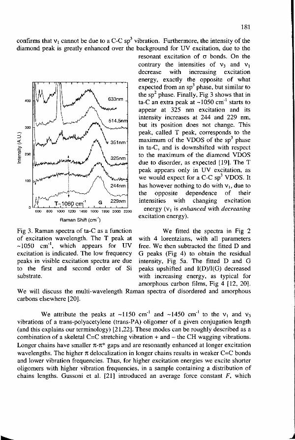
Fig 3. Raman spectra of ta-C as a function of excitation wavelength. The T peak at -1050 cm·1
, which appears for UV excitation is indicated. The low frequency peaks in visible excitation spectra are due to the first and second order of Si substrate.
energy, exactly the opposite of what expected from an sp3 phase, but similar to the sp2 phase. Finally, Fig 3 shows that in ta-C an extra peak at -1050 cm·1 starts to appear at 325 nm excitation and its intensity increases at 244 and 229 nm, but its position does not change. This peak, called T peak, corresponds to the maximum of the VDOS of the sp3 phase in ta-C, and is downshifted with respect to the maximum of the diamond VDOS due to disorder, as expected [19]. The T peak appears only in UV excitation, as we would expect for a C-C sp3 VDOS. It has however nothing to do with vh due to the opposite dependence of their intensities with changing excitation
energy (v 1 is enhanced with decreasing excitation energy).
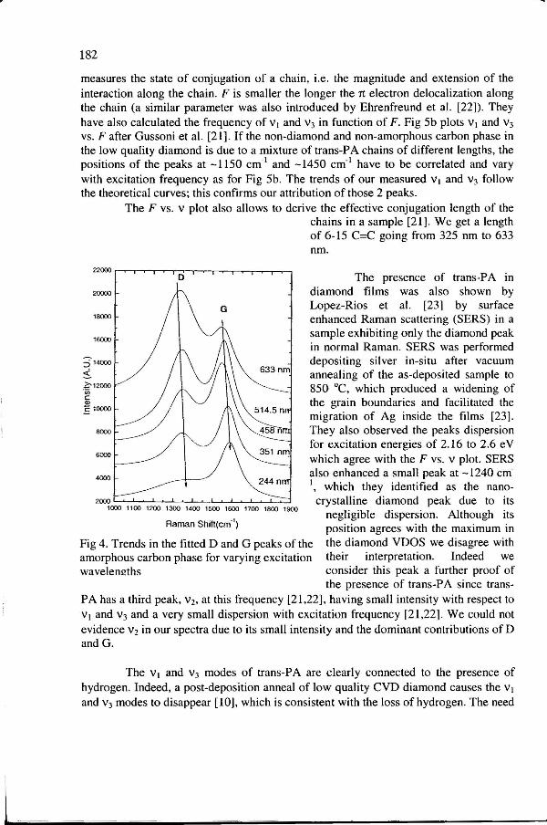
We fitted the spectra in Fig 2 with 4 lorentzians, with all parameters free. We then subtracted the fitted D and G peaks (Fig 4) to obtain the residual intensity, Fig Sa. The fitted D and G peaks upshifted and I(D)/I(G) decreased with increasing energy, as typical for amorphous carbon films, Fig 4 [12, 20].
We will discuss the multi-wavelength Raman spectra of disordered and amorphous carbons elsewhere [20].
We attribute the peaks at -1150 cm·1 and -1450 cm·1 to the v 1 and v3
vibrations of a trans-polyacetylene (trans-PA) oligomer of a given conjugation length (and this explains our terminology) [21,22]. These modes can be roughly described as a combination of a skeletal C=C stretching vibration + and - the CH wagging vibrations. Longer chains have smaller n-n* gaps and are resonantly enhanced at longer excitation wavelengths. The higher 7t delocalization in longer chains results in weaker C=C bonds and lower vibration frequencies. Thus, for higher excitation energies we excite shorter oligomers with higher vibration frequencies, in a sample containing a distribution of chains lengths. Gussoni et at. [21] introduced an average force constant F, which
r 182
measures the state of conjugation of a chain, i.e. the magnitude and extension of the interaction along the chain. F is smaller the longer the 1t electron delocalization along the chain (a similar parameter was also introduced by Ehrenfreund et al. [22]). They have also calculated the frequency of v 1 and v3 in function of F. Fig 5b plots v1 and v3
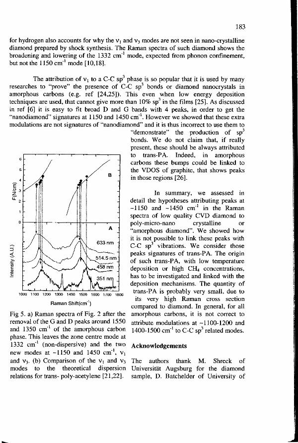
vs. F after Gussoni et al. [21]. If the non-diamond and non-amorphous carbon phase in the low quality diamond is due to a mixture of trans-PA chains of different lengths, the positions of the peaks at -1150 cm-1 and -1450 em·• have to be correlated and vary with excitation frequency as for Fig 5b. The trends of our measured v1 and v3 follow the theoretical curves; this confirms our attribution of those 2 peaks.
22000
20000
18000
16000
;14000
~ 1!'12000 ·u; c Q)
_s 10000
8000
6000
4000
The F vs. v plot also allows to derive the effective conjugation length of the chains in a sample [21]. We get a length of 6-15 C=C going from 325 nm to 633 nm.
0
G
The presence of trans-PA in diamond films was also shown by Lopez-Rios et al. [23] by surface enhanced Raman scattering (SERS) in a sample exhibiting only the diamond peak in normal Raman. SERS was performed depositing silver in-situ after vacuum annealing of the as-deposited sample to 850 °C, which produced a widening of the grain boundaries and facilitated the migration of Ag inside the films [23]. They also observed the peaks dispersion for excitation energies of 2.16 to 2.6 e V which agree with the F vs. v plot. SERS also enhanced a small peak at -1240 cm-1, which they identified as the nano-
2000 crystalline diamond peak due to its 1000 1100 1200 1300 1400 1500 1600 1700 1800 1900
Raman Shift(cm·'l
Fig 4. Trends in the fitted D and G peaks of the amorphous carbon phase for varying excitation wavelem!ths
negligible dispersion. Although its position agrees with the maximum in the diamond VDOS we disagree with their interpretation. Indeed we consider this peak a further proof of the presence of trans-P A since trans
PA has a third peak, v2, at this frequency [21,22], having small intensity with respect to v1 and v3 and a very small dispersion with excitation frequency [21,22]. We could not evidence v2 in our spectra due to its small intensity and the dominant contributions of D and G.
The v 1 and v3 modes of trans-PA are clearly connected to the presence of hydrogen. Indeed, a post-deposition anneal of low quality CVD diamond causes the v1
and v3 modes to disappear [ 10], which is consistent with the loss of hydrogen. The need
183
for hydrogen also accounts for why the v 1 and v3 modes are not seen in nano-crystalline diamond prepared by shock synthesis. The Raman spectra of such diamond shows the broadening and lowering of the 1332 em·• mode, expected from phonon confinement, but not the 1150 em·• mode [10,18}.
The attribution of v 1 to a C-C sp3 phase is so popular that it is used by many researches to "prove" the presence of C-C sp3 bonds or diamond nanocrystals in amorphous carbons (e.g. ref [24,25}). This even when low energy deposition techniques are used, that cannot give more than 10% sp3 in the films [25}. As discussed in ref [6} it is easy to fit broad D and G bands with 4 peaks, in order to get the "nanodiamond" signatures at 1150 and 1450 em·•. However we showed that these extra modulations are not signatures of "nanodiamond" and it is thus incorrect to use them to
6
5
e ~ 3 z i:L2
• B
1000 1100 1200 1300 1400 1500 1600 1700 1800
Raman Shift( em·')
Fig 5. a) Raman spectra of Fig. 2 after the removal ofthe G and D peaks around 1550 and 1350 em·• of the amorphous carbon phase. This leaves the zone centre mode at 1332 em·• (non-dispersive) and the two new modes at -1150 and 1450 em·•, v 1
and v3• (b) Comparison of the v 1 and v3
modes to the theoretical dispersion relations for trans- poly-acetylene [21 ,22}.
--
"demonstrate" the production of sp3
bonds. We do not claim that, if really present, these should be always attributed to trans-P A. Indeed, in amorphous carbons these bumps could be linked to the VDOS of graphite, that shows peaks in those regions [26} .
In summary, we assessed in detail the hypotheses attributing peaks at -1150 and -1450 em·• in the Raman spectra of low quality CVD diamond to poly-micro-nano crystalline or "amorphous diamond". We showed how it is not possible to link these peaks with C-C sp3 vibrations. We consider those peaks signatures of trans-PA. The origin of such trans-PA, with low temperature deposition or high CRt concentrations, has to be investigated and linked with the deposition mechanisms. The quantity of trans-PA is probably very small, due to its very high Raman cross section
compared to diamond. In general, for all amorphous carbons, it is not correct to attribute modulations at -1100-1200 and 1400-1500 em·• to C-C sp3 related modes.
Acknowledgements
The authors thank M. Shreck of Universitat Augsburg for the diamond sample, D. Batchelder of University of
184
Leeds, M. Stutzmann of Walter Schottky Institut Muenchen, M. Kuball of University of Bristol, D. Richards of Cavendish Laboratory, Cambridge, and G. Gibson of Materials Science and Metallurgy, Cambridge, for the access to Raman facilities. We thank C. Castiglioni for useful discussions on polyacetylenes. A.C.F. acknowledges funding from an E. U. Marie Curie fellowship.
References
I. W. A. Yarbrough, R. Messier, Science 247, 688 (1990) 2. D. S. Knight, W. B. White, J. Mater. Res . 4, 385 (1989) 3. J. C. Angus, C. C. Hayman, Science 241 , 913 (1988) 4. D. M. Gruen, Annu. Rev. Mater. Sci. 29, 211 (1999) S. M. Shreck, K. H. Thurer, B. Stritzker, J. Appl. Phys. 81,3092 (1997) 6. A. C. Ferrari, J . Robertson, Phys. Rev. B 61, 14095 (2000) 7. R. J. Nemanich, J. T. Glass, G. Lucovsky, R. E. Shroder, J. Vac. Sci. Techno!. A6, 1783 (1988); R. E.
Shroder, R. J. Nemanich, J. T. Glass, Phys. Rev. B 41, 3738 (1990). 8. K. Kobashi, K. Nishimura, Y. Kawate, T. Horiuchi, Phys. Rev. B 38, 4067 (1988) 9. K. Maruyama, M. Makino, N. Kikukawa, M. Shiraishi, J. Mat. Sci. Lett. 11, 116 (1992); S. R. P. Silva.
G. A. J. Amaratunga, E. K. H. Salje, K. M. Knowles, J. Mat. Sci. 29, 4962 (1994) 10. E. D. Obraztsova, V. L. Kuznetsov, E. N. Loubnin, S. M. Pimenov, V. G. Pereverzev, in Nanoparticles
in Solids and Solutions, p. 485, ed. by J. H. Fendler and I. Dekany, (Kuwler Academic publishers, 1996); L. C. Nistor, J. Van Landuyt, V. G. Ralchenko, E. D. Obratzova, A. A. Smolin, Diam. Relat. Mater. 6 , !59 (1997)
II. M. Nishitani-Gamo, T. Ando, K. Yamamoto, K. Watanabe, P. A. Denning, Y. Sato, M. Sekita, Appl. Phys. Lett . 70, I 530 (1997)
12. J. Wagner, M. Ramsteiner, C. Wild, P. Koidl, Phys. Rev. B, 40 1817 (1989); J. Wagner, C. Wild, P. Koidl, Appl. Phys. Lett. 59. 779 (1991)
13. B. Marcus, L. Fayette, M. Mermoux, L. Abello, G. Lucazeau, J. Appl. Phys. 76,3463 (1994) 14. K. Okada, H. Kanda, S. Komatsu, S. Matsumoto, J. Appl. Phys. 88, 1674 (2000) IS . P. Pavone, K. Karch, 0. Shutt, W. Windl, D. Strauch, P. Giannozzi , S. Baroni, Phys. Rev. B 48, 3164
(1993) 16. N. Wada, P. J. Gaczi and A. Solin, J. Non-cryst. Solids 35&36, 543 (1980); S. R. Salis, D. J. Gardiner,
M. Bowden, J. Savage and D. Rodway, Diam. Relat. Mater. 5, 589 (1996) 17. J. W. Ager III, D. K. Veirs , G. M. Rosenblatt, Phys. Rev. B 43, 6491 (1991) 18. M. Yoshikawa, Y. Mori, M. Meagawa, G. Katagiri , H. Ishida and A. Ishitani , Appl. Phys. Lett. 62,
3114 (1993); M. Yoshikawa, Y. Mori, H. Oabata, M. Maegawa, G. Katagiri , H. lshsida and A. Ishsitani , Appl. Phys. Lett. 67, 694 ( 1995)
19. K. W. R. Gilkes , H. S. Sands, D. N. Bathcelder, J. Roberston, W. I. Milne, Appl. Phys. Lett. 70, 1980 (1997); V. I. Merkulov, J. S. Lannin, C. H. Munro, S. A. Asher, V. S. Veerasamy, and W. I. Milne, Phys. Rev. Lett. 78, 4869 (1997)
20. A.C. Ferrari, J. Robertson, Phys. Rev. B. submitted (2000) 21. M. Gussoni, C. Castiglioni and G. Zerbi, Vibrational Spectroscopy of Polyconjugated Materials:
Polyacetylene and Polyenes, in Spectroscopy of Advanced Materials, ed by. R. J. Clark and R. E. Hester, p2Sl (John Wiley & Sons, 1991)
22. E. Ehrenfreund, Z. Vardeny, 0 . Brafrnan and B. Horovitz, Phys. Rev. B 36, 1535 (1987) 23. T. Lopez-Rios, E. Sandre'. S. Leclerq and E. Sauvain, Phys. Rev. Lett. 76, 4935 (1996) 24. J. Schwan, S. Ulrich, V. Batori, H. Ehrhardt, S. R. P. Silva, J. Appl. Phys. 80, 440 (1996) 25. S. Bhargava, H. D. Bist. A. V. Narlikar, S. B. Samanta, J. Narayan and H. B. Tripathi, J. Appl. Phys.
79. 1917 (1996) 26. F. Li and J. S. Lanoin, Appl. Phys. Lett. 61, 2116 (1992)


![CO2 laser micromachining of nanocrystalline diamond films ...2016).pdf · diamond at these wavelengths. Albin et al. [10] observed laser induced damage of polycrystalline diamond](https://img.pdfslide.net/doc/110x75/60a8c0bf591bf103494c5683/co2-laser-micromachining-of-nanocrystalline-diamond-films-2016pdf-diamond.jpg)