Embed Size (px)
Citation preview
Fiber draw synthesisNicholas D. Orfa,b, Ofer Shapiraa, Fabien Sorina,b, Sylvain Dantoa, Marc A. Baldoc,John D. Joannopoulosd, and Yoel Finka,b,1
aResearch Laboratory of Electronics, bDepartment of Materials Science and Engineering, cDepartment of Electrical Engineering and Computer Science,and dDepartment of Physics, Massachusetts Institute of Technology, 77 Massachusetts Avenue, Cambridge, MA 02139
Contributed by John D. Joannopoulos, January 24, 2011 (sent for review December 22, 2010)
The synthesis of a high-melting temperature semiconductor in alow-temperature fiber drawing process is demonstrated, substan-tially expanding the set of materials that can be incorporatedinto fibers. Reagents in the solid state are arranged in proximatedomains within a fiber preform. The preform is fluidized at ele-vated temperatures and drawn into fiber, reducing the lateraldimensions and bringing the domains into intimate contact toenable chemical reaction. A polymer preform containing a thinlayer of selenium contacted by tin–zinc wires is drawn to yield elec-trically contacted crystalline ZnSe domains of sub-100-nm scales.The in situ synthesized compound semiconductor becomes thebasis for an electronic heterostructure diode of arbitrary lengthin the fiber. The ability to synthesize materials within fibers whileprecisely controlling their geometry and electrical connectivity atsubmicron scales presents new opportunities for increasing thecomplexity and functionality of fiber structures.
flexible electronics ∣ optical fiber processing ∣ semiconductor device
Thermal fiber drawing is a process in which a macrostructuredpreform is heated and drawn into extended lengths of micro-
structured fiber. New methods of increasing both the structuralcomplexity of fibers and number of materials compatible with thedrawing process are substantially expanding the functionality ofphotonic crystal and semiconductor device fibers (1–3). Thedrawing process, however, has until now been limited to materialsthat flow at the draw temperature. Approaches that attempt tocircumvent this limitation include depositing materials inside(4–7) or onto the surface (8–11) of previously drawn fiber sub-strates. These methods do not take full advantage of the scalingassociated with fiber drawing and are limited in their geometriccomplexity and the length over which uniform structures can beproduced. Here this seemingly fundamental limitation is lifted byutilizing the fiber drawing process to synthesize in situ a chemicalcompound that has a melting temperature far exceeding the drawtemperature. In this process, precursors are arranged in adjacentdomains in a macroscopic preform. During thermal drawing,the fluid reactants come into contact and precipitate a new com-pound. To demonstrate the potential of this fiber draw synthesismethod, a polymer fiber preform containing a thin selenium–
sulfur layer next to eutectic tin–zinc wires is constructed and ther-mally codrawn into a fiber consisting of electrically contactedcrystalline ZnSe domains of sub-100-nm scales at the interfacebetween the metallic domains and selenium layer. The formationof the interface compound is the basis for an electronic hetero-structure and a thermally drawn fiber device exhibiting rectifyingbehavior. The ability to synthesize materials during the fiberdraw process while maintaining precise and arbitrary geometriesshould lead to substantial advances in the form and function offibers.
Results and DiscussionA fiber preform consisting of metallic Sn74Pb26 and Sn85Zn15wires placed within an amorphous polymer cladding and spannedby a thin film of Se97S3 was constructed and drawn into anextended fiber (schematic drawings and SEM micrographs ofthe preform and fiber are shown in Fig. 1). The metal electrodeswere placed in an alternating fashion such that each Sn74Pb26∕
Se97S3∕Sn85Zn15 combination forms an independently addressa-ble electronic device. Neither the elemental selenium nor zincreactants are liquid at the drawing temperature and thus incom-patible with thermal drawing. However, the melting tempera-ture of both reactants can be depressed by alloying with eithersulfur (in the case of selenium) or tin (for the zinc reactant).Upon exiting the drawing furnace, the selenium alloy is quenchedinto the amorphous state, but it easily devitrifies to the equili-brium crystalline phase when annealed for 1 h at 150 °C (12)(seeMethods for full experimental details). The distance betweenthe metal electrodes in a single fiber device is approximately15 μm, an order-of-magnitude smaller than previous compositedevice fibers, suggesting that significant device miniaturizationand concomitant increases in device performance and densityare possible in future fiber devices (13).
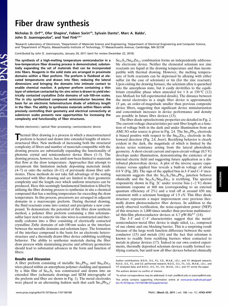
The fiber diode optoelectronic properties are detailed in Fig. 2.The current-voltage characteristics per unit fiber length as a func-tion of voltage both in the dark and under illumination from anAM1.5G solar source is given in Fig. 2A. The Sn74Pb26 electrodeis biased positive with respect to the Sn85Zn15 electrode in theforward direction (Fig. 2A, Inset). Rectifying behavior is clearlyevident in the dark, the magnitude of which is limited by thedevice series resistance arising from the lateral photodiodegeometry. A short-circuit current and open-circuit voltage (0.5 V)develops under illumination, demonstrating the existence of aninternal electric field and suggesting future application as a dis-tributed photovoltaic device. A plot of the inverse square capa-citance versus applied bias reveals a built-in voltage of about0.8 V (Fig. 2B). The sign of the applied bias in I–Vand C–V mea-surements suggests that the Se97S3∕Sn74Pb26 junction behavesohmically and the Se97S3∕Sn85Zn15 is rectifying. The spectralresponsivity shown in Fig. 2C under reverse bias (−2 V) showsmaximum response at 460 nm (corresponding to an externalquantum efficiency of 2%) and a trail off at around 650 nm,consistent with a selenium bandgap of 1.9 eV. This fiber diodestructure represents a major improvement over previous ther-mally drawn photoconductor fiber devices. In addition to thenewly observed rectification, the noise-equivalent power (NEP)of this structure is 1,000 times smaller than previous multimater-ial thin-film photoconductor devices at 4.7 pW-Hz0.5 (14).
The I–V and C–V characteristics suggest that the metal-semiconductor-metal fiber device is single sided, i.e., composedof one ohmic and one blocking barrier. This is a surprising resultbecause of the large work function difference between the semi-conductor (15) and metals (16) and the fact that selenium isknown to readily form rectifying barriers when contacted tometals in planar devices (17). Indeed in our own control experi-ments, thermally deposited selenium devices readily formed rec-tifying contacts, but until now all fiber devices behaved ohmically
Author contributions: N.D.O., O.S., F.S., S.D., M.A.B., J.D.J., and Y.F. designed research;N.D.O., O.S., F.S., and S.D. performed research; N.D.O., O.S., F.S., S.D., M.A.B., J.D.J., andY.F. analyzed data; and N.D.O., O.S., F.S., S.D., M.A.B., J.D.J., and Y.F. wrote the paper.
The authors declare no conflict of interest.1To whom correspondence may be addressed. E-mail: [email protected] or [email protected].
This article contains supporting information online at www.pnas.org/lookup/suppl/doi:10.1073/pnas.1101160108/-/DCSupplemental.
www.pnas.org/cgi/doi/10.1073/pnas.1101160108 PNAS ∣ March 22, 2011 ∣ vol. 108 ∣ no. 12 ∣ 4743–4747
ENGINEE
RING
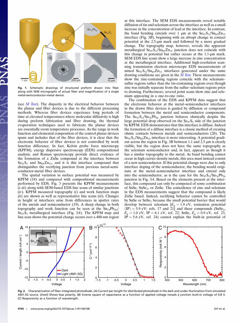
(see SI Text). The disparity in the electrical behavior betweenthe planar and fiber devices is due to the different processingmethods. Whereas fiber devices experience long periods oftime at elevated temperatures where molecular diffusivity is highduring preform fabrication and fiber drawing, the thermalevaporation techniques used to fabricate the planar devicesare essentially room temperature processes. As the range in workfunction and elemental composition of the control planar devicesspans and includes that of the fiber devices, it is clear that theelectronic behavior of fiber devices is not controlled by workfunction difference. In fact, Kelvin probe force microscopy(KPFM), energy dispersive spectroscopy (EDS) compositionalanalysis, and Raman spectroscopy provide direct evidence ofthe formation of a ZnSe compound at the interface betweenSe97S3 and Sn85Zn15, and it is this interface compound thatdistinguishes the rectifying junction from previous metal-semi-conductor-metal fiber devices.
The spatial variation in surface potential was measured byKPFM (18) and compared with compositional measurementsperformed by EDS. Fig. 3 presents the KPFM measurements(i–iii) along with SEM-based EDS line scans of similar junctions(iv). KPFM measured topography (i) and work function maps(ii) are shown as well as representative line scans (iii). Changesin height at interfaces arise from differences in sputter ratesof the metals and semiconductor (19). A sharp change in bothtopography and work function can be seen at the Sn74Pb26∕Se97S3 metallurgical interface (Fig. 3A). The KPFM map andline scan shows the potential change occurs over a 400-nm region
at this interface. The SEM EDS measurements reveal notablediffusion of tin and selenium across the interface as well as a smallincrease in the concentration of lead at the interface. In contrast,the band bending extends over 1 μm at the Se97S3∕Sn85Zn15interface (Fig. 3B), beginning with an abrupt change in contactpotential at the 2.5-μm mark and followed by a more gradualchange. The topography map, however, reveals the apparentmetallurgical Se97S3∕Sn85Zn15 junction does not coincide withthis change in potential but rather occurs at the 1.1-μm mark.SEM EDS line scans show a large increase in zinc concentrationat the metallurgical interface. Additional high-resolution scan-ning transmission electron microscope EDS measurements ofmixed Se97S3∕Sn85Zn15 interfaces generated under the samedrawing conditions are given in the SI Text. These measurementsshow the zinc-containing regions coincide with the selenium–
sulfur regions rather than the tin-containing regions even thoughzinc was initially separate from the sulfur–selenium regions priorto drawing. Furthermore, several point scans show zinc and sele-nium appearing in a one-to-one ratio.
The combination of the EDS and KPFM data suggest thatthe electronic behavior at the metal–semiconductor interfacesin the drawn fiber devices is guided by diffusion or compoundformation between the metal and semiconductor components.The Se97S3∕Sn74Pb26 junction behaves ohmically despite thelarge potential drop observed on the Se97S3 side of the junctionby KPFM. EDS demonstrates that this interface is diffuse. Indeedthe formation of a diffuse interface is a classic method of creatingohmic contacts between metals and semiconductors (20). TheSe97S3∕Sn85Zn15 interface is more interesting. A potential gradi-ent across the region in Fig. 3B between 1.1 and 2.5 μm is clearlyvisible, but the region does not have the same topography asthe selenium semiconductor and, in fact, appears as though ithas a similar topography to the metal. As band bending cannotoccur in high carrier density metals, this area must instead consistof a new semiconductor. If this potential change were due to onlyinterface doping of the semiconductor, the bending would origi-nate at the metal–semiconductor interface and extend onlyinto the semiconductor, as is the case for the Se97S3∕Sn74Pb26junction in Fig. 3A. Based on the elements present at the inter-face, this compound can only be composed of some combinationof SnSe, SnSe2, or ZnSe. The coincidence of zinc and seleniumin the EDS measurements suggest that the compound is likelyZnSe based. Indeed, rectifying behavior cannot be controlledby SnSe or SnSe2 because the small potential barrier that woulddevelop between selenium [Eg ¼ 1.9 eV, ionization potentialðIPÞ ¼ 5.9 eV; refs. 17 and 21] and these compounds (SnSe2,Eg ¼ 1.0 eV, IP ¼ 6.1 eV, ref. 22; SnSe, Eg ¼ 0.9 eV, ref. 23,IP ¼ 5.6 eV, ref. 24) cannot explain the built-in potential of
Fig. 1. Schematic drawings of structured preform drawn into fiberalong with SEM micrographs of actual fiber and magnification of a singlemetal-semiconductor-metal device.
-1.5 -1 -0.5 0 0.5 1 1.50
2
4
6
8
10x 1013
Voltage
C-2 (
cm2
F-2)
-2 -1.5 -1 -0.5 0 0.5 1 1.5 2-15
-10
-5
0
5
10
15
Voltage
Cur
rent
/ le
ngth
(nA
cm
-1)
DarkLight (AM1.5G)
Sn74Pb26 Sn85Zn15
A B C
400 500 600 700 8000
2
4
6
8
10
Wavelength (nm)
Res
pons
ivity
(m
A W
-1)
Fig. 2. Characterization of fiber-integrated photodiode. (A) Current per length for distributed photodiode in the dark and under illumination from simulatedAM1.5G source. (Inset) Shows bias polarity. (B) Inverse square of capacitance as a function of applied voltage reveals a junction built-in voltage of 0.8 V.(C) Responsivity as a function of wavelength.
4744 ∣ www.pnas.org/cgi/doi/10.1073/pnas.1101160108 Orf et al.
0.8 V determined by both C–V and KPFM measurements.Furthermore there were no signs of this compound formationat the Se97S3∕Sn74Pb26 interface even though SnSe and SnSe2would be just as likely to form at either interface due to theequally high concentration of tin and selenium at both junctions.A large bandgap semiconductor such as zinc selenide (Eg ¼2.7 eV, IP ¼ 6.8 eV) (25) would, however, form a barrier tohole conduction and explain the rectifying behavior. Additionalmacroscopic X-ray diffraction measurements performed on zincpieces incubated in molten selenium at the fiber drawing tem-perature (260 °C) confirm that crystalline ZnSe can form atthe drawing temperature (see SI Text).
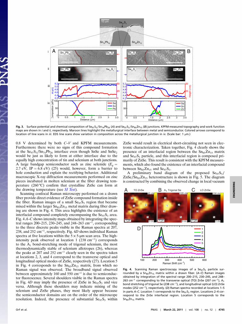
Scanning confocal Raman microscopy performed on a drawnfiber provide direct evidence of ZnSe compound formation insidethe fiber. Raman images of a small Se97S3 region that becamemixed within the larger Sn85Zn15 metal matrix during fiber draw-ing are shown in Fig. 4. This area highlights the existence of aninterfacial compound completely encompassing the Se97S3 area.Fig. 4 A–C shows intensity maps obtained by integrating the spec-tral ranges 200–215, 230–245, and 248–263 cm−1, correspondingto the three discrete peaks visible in the Raman spectra at 207,238, and 252 cm−1, respectively. Fig. 4D shows individual Ramanspectra at five locations within the 5 × 5-μm scan area. The high-intensity peak observed at location 1 (238 cm−1) correspondsto the A1 bond-stretching mode of trigonal selenium, the mostthermodynamically stable of selenium allotropes (26), whereasthe peaks at 207 and 252 cm−1 clearly seen in the spectra takenat locations 2, 3, and 4 correspond to the transverse optical andlongitudinal optical modes of ZnSe, respectively (27). Location 5in Fig. 4 corresponds to the Sn85Zn15 matrix, from which noRaman signal was observed. The broadband signal observedbetween approximately 160 and 550 cm−1 is due to semiconduc-tor fluorescence. Several shoulders visible in the Raman spectrain Fig. 4D may imply the presence of ZnSe in Se97S3 and viceversa. Although these shoulders may indicate mixing of theselenium and ZnSe phases, they most likely appear becausethe semiconductor domains are on the order of the microscoperesolution. Indeed, the presence of substantial Se97S3 within
ZnSe would result in electrical short-circuiting not seen in elec-tronic characterization. Taken together, Fig. 4 clearly shows thepresence of an interfacial region between the Sn85Zn15 matrixand Se97S3 particle, and this interfacial region is composed pri-marily of ZnSe. This result is consistent with the KPFMmeasure-ments, which also found the existence of an interfacial compoundbetween Sn85Zn15 and Se97S3.
A preliminary band diagram of the proposed Se97S3∕ZnSe∕Sn85Zn15 heterostructure is shown in Fig. 5. The diagramis constructed by combining the observed change in local vacuum
A B
Fig. 3. Surface potential and chemical composition of Se97S3∕Sn74Pb26 (A) and Se97S3∕Sn85Zn15 (B) junctions. KPFM-measured topography and work functionmaps are shown in i and ii, respectively. Maroon lines highlight the metallurgical interface between metal and semiconductor. Colored arrows correspond tolocation of line scans in iii. EDS line scans show variation in composition across the metallurgical junction in iv. (Scale bar: 1 μm.)
111 222
333
444
555
TO ZnSe LO ZnSeA1 Trigonal Se
0 cts
45 cts 105 cts 230 cts
0 cts 0 cts1 µm
A B C
1 µm1 µm
D
100 200 300 400 500 600Raman Shift (cm−1)
12345
Fig. 4. Scanning Raman spectroscopy images of a Se97S3 particle sur-rounded by a Sn85Zn15 matrix within a drawn fiber. (A–C) Raman imagesobtained by integration of the spectral range 200–215, 230–245, and 248–263 cm−1 corresponding to the transverse optical (TO) ZnSe (207 cm−1), A1
bond stretching of trigonal Se (238 cm−1), and longitudinal optical (LO) ZnSemodes (252 cm−1), respectively. (D) Raman spectra recorded at locations 1–5in parts A–C. Location 1 corresponds to the Se97S3 region. Locations 2–4 cor-respond to the ZnSe interfacial region. Location 5 corresponds to theSn85Zn15 matrix.
Orf et al. PNAS ∣ March 22, 2011 ∣ vol. 108 ∣ no. 12 ∣ 4745
ENGINEE
RING
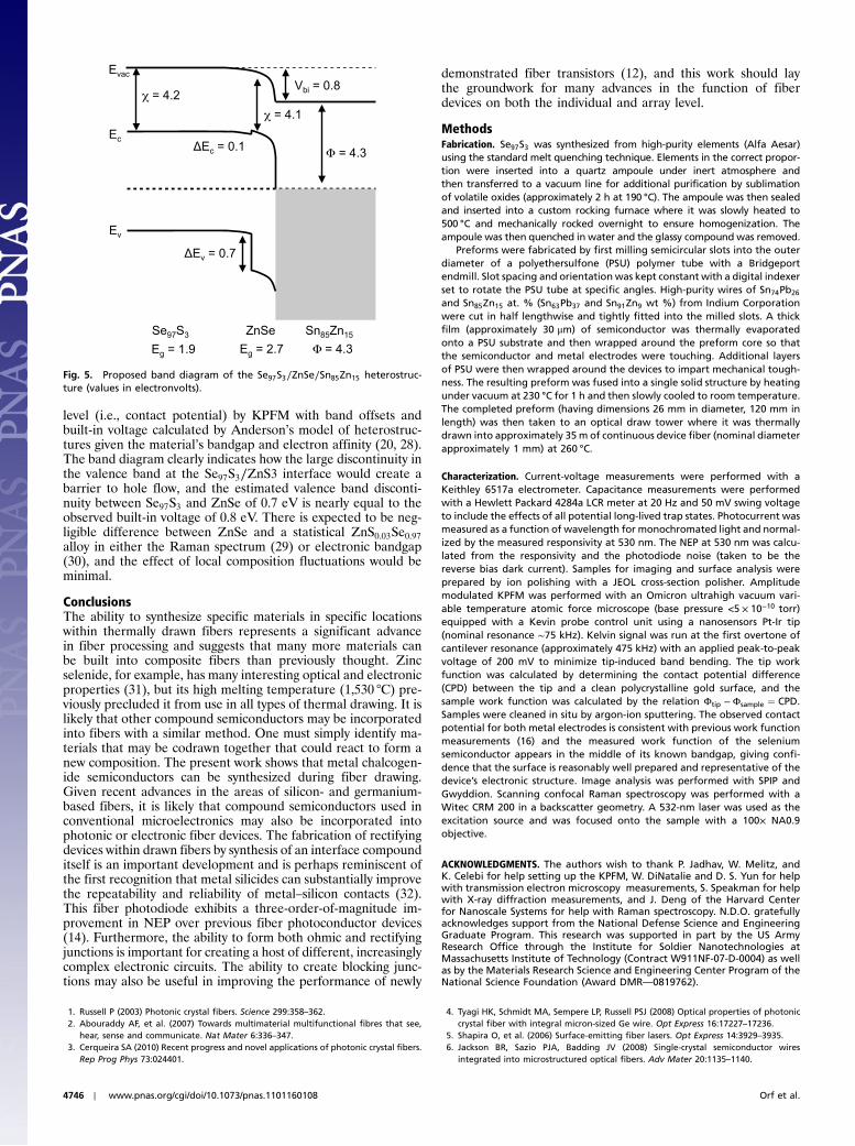
level (i.e., contact potential) by KPFM with band offsets andbuilt-in voltage calculated by Anderson’s model of heterostruc-tures given the material’s bandgap and electron affinity (20, 28).The band diagram clearly indicates how the large discontinuity inthe valence band at the Se97S3∕ZnS3 interface would create abarrier to hole flow, and the estimated valence band disconti-nuity between Se97S3 and ZnSe of 0.7 eV is nearly equal to theobserved built-in voltage of 0.8 eV. There is expected to be neg-ligible difference between ZnSe and a statistical ZnS0.03Se0.97alloy in either the Raman spectrum (29) or electronic bandgap(30), and the effect of local composition fluctuations would beminimal.
ConclusionsThe ability to synthesize specific materials in specific locationswithin thermally drawn fibers represents a significant advancein fiber processing and suggests that many more materials canbe built into composite fibers than previously thought. Zincselenide, for example, has many interesting optical and electronicproperties (31), but its high melting temperature (1,530 °C) pre-viously precluded it from use in all types of thermal drawing. It islikely that other compound semiconductors may be incorporatedinto fibers with a similar method. One must simply identify ma-terials that may be codrawn together that could react to form anew composition. The present work shows that metal chalcogen-ide semiconductors can be synthesized during fiber drawing.Given recent advances in the areas of silicon- and germanium-based fibers, it is likely that compound semiconductors used inconventional microelectronics may also be incorporated intophotonic or electronic fiber devices. The fabrication of rectifyingdevices within drawn fibers by synthesis of an interface compounditself is an important development and is perhaps reminiscent ofthe first recognition that metal silicides can substantially improvethe repeatability and reliability of metal–silicon contacts (32).This fiber photodiode exhibits a three-order-of-magnitude im-provement in NEP over previous fiber photoconductor devices(14). Furthermore, the ability to form both ohmic and rectifyingjunctions is important for creating a host of different, increasinglycomplex electronic circuits. The ability to create blocking junc-tions may also be useful in improving the performance of newly
demonstrated fiber transistors (12), and this work should laythe groundwork for many advances in the function of fiberdevices on both the individual and array level.
MethodsFabrication. Se97S3 was synthesized from high-purity elements (Alfa Aesar)using the standard melt quenching technique. Elements in the correct propor-tion were inserted into a quartz ampoule under inert atmosphere andthen transferred to a vacuum line for additional purification by sublimationof volatile oxides (approximately 2 h at 190 °C). The ampoule was then sealedand inserted into a custom rocking furnace where it was slowly heated to500 °C and mechanically rocked overnight to ensure homogenization. Theampoule was then quenched in water and the glassy compound was removed.
Preforms were fabricated by first milling semicircular slots into the outerdiameter of a polyethersulfone (PSU) polymer tube with a Bridgeportendmill. Slot spacing and orientation was kept constant with a digital indexerset to rotate the PSU tube at specific angles. High-purity wires of Sn74Pb26
and Sn85Zn15 at. % (Sn63Pb37 and Sn91Zn9 wt %) from Indium Corporationwere cut in half lengthwise and tightly fitted into the milled slots. A thickfilm (approximately 30 μm) of semiconductor was thermally evaporatedonto a PSU substrate and then wrapped around the preform core so thatthe semiconductor and metal electrodes were touching. Additional layersof PSU were then wrapped around the devices to impart mechanical tough-ness. The resulting preform was fused into a single solid structure by heatingunder vacuum at 230 °C for 1 h and then slowly cooled to room temperature.The completed preform (having dimensions 26 mm in diameter, 120 mm inlength) was then taken to an optical draw tower where it was thermallydrawn into approximately 35 m of continuous device fiber (nominal diameterapproximately 1 mm) at 260 °C.
Characterization. Current-voltage measurements were performed with aKeithley 6517a electrometer. Capacitance measurements were performedwith a Hewlett Packard 4284a LCR meter at 20 Hz and 50 mV swing voltageto include the effects of all potential long-lived trap states. Photocurrent wasmeasured as a function of wavelength for monochromated light and normal-ized by the measured responsivity at 530 nm. The NEP at 530 nm was calcu-lated from the responsivity and the photodiode noise (taken to be thereverse bias dark current). Samples for imaging and surface analysis wereprepared by ion polishing with a JEOL cross-section polisher. Amplitudemodulated KPFM was performed with an Omicron ultrahigh vacuum vari-able temperature atomic force microscope (base pressure <5 × 10⁻¹⁰ torr)equipped with a Kevin probe control unit using a nanosensors Pt-Ir tip(nominal resonance ∼75 kHz). Kelvin signal was run at the first overtone ofcantilever resonance (approximately 475 kHz) with an applied peak-to-peakvoltage of 200 mV to minimize tip-induced band bending. The tip workfunction was calculated by determining the contact potential difference(CPD) between the tip and a clean polycrystalline gold surface, and thesample work function was calculated by the relation Φtip −Φsample ¼ CPD.Samples were cleaned in situ by argon-ion sputtering. The observed contactpotential for both metal electrodes is consistent with previous work functionmeasurements (16) and the measured work function of the seleniumsemiconductor appears in the middle of its known bandgap, giving confi-dence that the surface is reasonably well prepared and representative of thedevice’s electronic structure. Image analysis was performed with SPIP andGwyddion. Scanning confocal Raman spectroscopy was performed with aWitec CRM 200 in a backscatter geometry. A 532-nm laser was used as theexcitation source and was focused onto the sample with a 100× NA0.9objective.
ACKNOWLEDGMENTS. The authors wish to thank P. Jadhav, W. Melitz, andK. Celebi for help setting up the KPFM, W. DiNatalie and D. S. Yun for helpwith transmission electron microscopy measurements, S. Speakman for helpwith X-ray diffraction measurements, and J. Deng of the Harvard Centerfor Nanoscale Systems for help with Raman spectroscopy. N.D.O. gratefullyacknowledges support from the National Defense Science and EngineeringGraduate Program. This research was supported in part by the US ArmyResearch Office through the Institute for Soldier Nanotechnologies atMassachusetts Institute of Technology (Contract W911NF-07-D-0004) as wellas by the Materials Research Science and Engineering Center Program of theNational Science Foundation (Award DMR—0819762).
1. Russell P (2003) Photonic crystal fibers. Science 299:358–362.2. Abouraddy AF, et al. (2007) Towards multimaterial multifunctional fibres that see,
hear, sense and communicate. Nat Mater 6:336–347.3. Cerqueira SA (2010) Recent progress and novel applications of photonic crystal fibers.
Rep Prog Phys 73:024401.
4. Tyagi HK, Schmidt MA, Sempere LP, Russell PSJ (2008) Optical properties of photoniccrystal fiber with integral micron-sized Ge wire. Opt Express 16:17227–17236.
5. Shapira O, et al. (2006) Surface-emitting fiber lasers. Opt Express 14:3929–3935.6. Jackson BR, Sazio PJA, Badding JV (2008) Single-crystal semiconductor wires
integrated into microstructured optical fibers. Adv Mater 20:1135–1140.
Fig. 5. Proposed band diagram of the Se97S3∕ZnSe∕Sn85Zn15 heterostruc-ture (values in electronvolts).
4746 ∣ www.pnas.org/cgi/doi/10.1073/pnas.1101160108 Orf et al.

7. Sazio PJA, et al. (2006) Microstructured optical fibers as high-pressure microfluidicreactors. Science 311:1583–1586.
8. O'Connor B, Pipe KP, Shtein M (2008) Fiber based organic photovoltaic devices. ApplPhys Lett 92:193306.
9. Liu JW, Namboothiry MAG, Carroll DL (2007) Fiber-based architectures for organicphotovoltaics. Appl Phys Lett 90:063501.
10. Liu JW, Namboothiry MAG, Carroll DL (2007) Optical geometries for fiber-basedorganic photovoltaics. Appl Phys Lett 90:133515.
11. Lee MR, et al. (2009) Solar power wires based on organic photovoltaic materials.Science 324:232–235.
12. Danto S, et al. (2010) Fiber field-effect device via in situ channel crystallization.Adv Mater 22:4162–4166.
13. Bayindir M, et al. (2005) Integrated fibres for self-monitored optical transport.Nat Mater 4:820–825.
14. Sorin F, et al. (2007) Multimaterial photodetecting fibers: A geometric and structuralstudy. Adv Mater 19:3872–3877.
15. Lide DR (2008) CRC Handbook of Chemistry and Physics (CRC, New York), pp 12–114.16. Orf N, Baikie I, Shapira O, Fink Y (2009)Work function engineering in low temperature
alloys. Appl Phys Lett 94:113504.17. Champness CH, Chan A (1985) Relation between barrier height and work function in
contacts to selenium. J Appl Phys 57:4823–4825.18. Sommerhalter C, Matthes TW, Glatzel T, Jager-Waldau A, Lux-Steiner MC (1999) High-
sensitivity quantitative Kelvin probe microscopy by noncontact ultra-high-vacuumatomic force microscopy. Appl Phys Lett 75:286–288.
19. Seah MP, Clifford CA, Green FM, Gilmore IS (2005) An accurate semi-empiricalequation for sputtering yields I: For argon ions. Surf Interface Anal 37:444–458.
20. Sze S (1981) Physics of Semiconductor Devices (Wiley Interscience, New York), 2nd Ed,,pp 122–129, pp 304–306.
21. Williams RH, Polanco JI (1974) Electronic-structure of chalcogenide solids—photoemission study of ordered and disordered selenium and tellurium. J Phys C: SolidState Phys 7:2745–2759.
22. Schlaf R, Pettenkofer C, Jaegermann W (1999) Band lineup of a SnS2/SnSe2/SnS2
semiconductor quantumwell structure prepared by van der Waals epitaxy. J Appl Phys
85:6550–6556.
23. Madelung O, Rössler U, Schulz M, eds. (1998) Tin Selenide (SnSe) Band Stucture,
Energy Gap, Effective Masses (SpringerMaterials, New York), The Landolt-Börnstein
Database, 41C.
24. Bennouna A, Priol M, Seignac A (1988) Experimental density of states of tin selenide
measurement on thin-films. Thin Solid Films 164:69–73.
25. Chiang TC, Himpsel FJ (2006) ZnSe. Electronic Structure of Solids: Photoemission
Spectra and Related Data, Landolt-Bornstein Group III, eds A Goldmann and EE Koch
(Springer Verlang, New York), Vol 23a, pp 81–84.
26. Nagata K, Ishibashi K, Miyamoto Y (1981) Raman and infrared-spectra of rhombohe-
dral selenium. Jpn J Appl Phys 20:463–469.
27. Taylor W (1967) Raman Spectra of cubic zinc selenide and telluride. Phys Lett A
24:556–558.
28. Milnes AG, Feucht DL (1972) Heterojunctions and Metal-Semiconductor Junctions
(Academic, New York), pp 1–43.
29. Gupta P, Bhattacharyya D, Chaudhuri S, Pal AK (1992) Preparation and characteriza-
tion of polycrystalline Znsxse1-X films prepared by a 2-zone hot wall technique. Thin
Solid Films 221:154–159.
30. Ebina A, Fukunaga E, Takahash T (1974) Variation with composition of E0 and E0þDelta-0 gaps in ZnSXSe1−X alloys. Phys Rev B: Condens Matter Mater Phys
10:2495–2500.
31. Kale RB, Lokhande CD (2004) Room temperature deposition of ZnSe thin films by
successive ionic layer adsorption and reaction (SILAR) method. Mater Res Bull
39:1829–1839.
32. Zhang S-L, Ostling M (2003) Metal silicides in CMOS technology: Past, present, and
future trends. Crit Rev Solid State Mater Sci 28:1–129.
Orf et al. PNAS ∣ March 22, 2011 ∣ vol. 108 ∣ no. 12 ∣ 4747
ENGINEE
RING
![Synthesis of Poly-Sodium-Acrylate (PSA)-Coated Magnetic ... · as the draw solute. Others [7,17] report the use of (24–48 %, wt %) PSA draw solute (in the form of free polyelectrolyte](https://img.pdfslide.net/doc/110x75/605f52742e685b3632287e96/synthesis-of-poly-sodium-acrylate-psa-coated-magnetic-as-the-draw-solute.jpg)