Embed Size (px)
Citation preview

ANSI/ISA-S50.02-1992
Approved May 17, 1994
American National Standard
Fieldbus Standard for Use in
Industrial Control Systems
Part 2: Physical Layer
Specification and
Service Definition

ANSI/ISA-S50.02 — Fieldbus Standard for Use in Industrial Control Systems, Part 2: Physical Layer Specification and Service Definition
ISBN 1-55617-317-2
Copyright 1992 by the Instrument Society of America. All rights reserved. Printed in the UnitedStates of America. No part of this publication may be reproduced, stored in a retrieval system, ortransmitted in any form or by any means (electronic, mechanical, photocopying, recording, orotherwise), without the prior written permission of the publisher.
ISA67 Alexander DriveP.O. Box 12277Research Triangle Park, North Carolina 27709

Preface
This preface is included for informational purposes and is not part of ISA-S50.02.
This standard has been prepared as part of the service of ISA toward a goal of uniformity in the field of instrumentation. To be of real value, this document should not be static, but should be subject to periodic review. Toward this end, the Society welcomes all comments and criticisms, and asks that they be addressed to the Secretary, Standards and Practices Board, ISA, 67 Alexander Drive, P. O. Box 12277, Research Triangle Park, NC 27709, Telephone (919) 549-8411, Fax (919) 549-8288, e-mail: [email protected].
ISA Standards and Practices Department is aware of the growing need for attention to the metric system of units in general, and the International System of Units (SI) in particular, in the preparation of instrumentation standards. The Department is further aware of the benefits to U.S.A. users of ISA standards of incorporating suitable references to the SI (and the metric system) in their business and professional dealings with other countries. Toward this end, this Department will endeavor to introduce SI-acceptable metric units in all new and revised standards to the greatest extent possible. The Metric Practice Guide, which has been published by the Institute of Electrical and Electronics Engineers as ANSI/IEEE Std. 268 1982, and future revisions, will be the reference guide for definitions, symbols, abbreviations, and conversion factors.
It is the policy of ISA to encourage and welcome the participation of all concerned individuals and interests in the development of ISA standards. Participation in ISA standards-making process by an individual in no way constitutes endorsement by the employer of that individual, of ISA, or of any of the standards that ISA develops.
This standard has been developed in cooperation with IEC SC65C/WG6, "Message data format for information transferred on process and control data highways." ISA committee and the IEC working group held concurrent meetings and have harmonized the developing drafts throughout the standards process. The IEC draft is currently at the Draft International Standard stage.
The following people served as members of ISA Subcommittee SP50.02:
NAME COMPANY
M. Zielinski, Chairman Rosemount, Inc.J. Elias, Editor Honeywell, Inc.C. Akiyama Yokogawa Electric CorporationT. Bowker Action Instruments, Inc.P. Burton ERA Technology, Ltd.P. Certiat TelemecaniqueJ. Geer ITT BartonF. Houvig Drexelbrook Engineering CompanyJ. Howard The Foxboro CompanyK. Kakizakai Fuji Electric Company, Ltd.M. Kogure Hitachi, Ltd.H. Landet Center for Industrial Research
ANSI/ISA-S50.02-1992 3

F. McKenna BP International, Ltd.E. Miller, Jr. South West Research InstituteB. Neve PACS, Ltd.P. Patel Del Mar ScientificT. Phinney Honeywell, Inc.R. Lloyd AMP, Inc.D. Simpson Masoneilan-DresserB. Squires Measurement Technology, Ltd.G. Tapperson Fisher Controls International, Inc.T. Tottori M-System Company, Ltd.C. Vaidya National Semiconductor
The following people served as members of ISA Committee SP50:
NAME COMPANY
C. Langford, Chairman E. I. du Pont de Nemours & CompanyC. Gross, Managing Director Dow Chemical CompanyK. Lindner, Managing Director Endress & Hauser GmbH & CompanyC. Akiyama Yokogawa Electric CorporationW. Baker Bailey Controls CompanyT. Bozarth Honeywell, Inc.P. Burton ERA Technology, Ltd.E. Butteriss Bechtel CompanyR. Caro Arthur D. Little, Inc.R. Crowder Ship Star Associates, Inc.E. Delahostria Allen-Bradley CompanyU. Dobrich Siemens AGB. Dumortier TelemecaniqueP. Early Texas Instruments, Inc.S. Glaser Dow Chemical CompanyB. Gross General Motors CorporationA. Gupta ABB Kent-Taylor, Inc.B. Hampton Shell Oil CompanyJ. Howard The Foxboro CompanyM. Kazahaya Fischer & Porter CompanyR. Ketcham Union Carbide CorporationR. Lasher Exxon Company USAJ. Lesnau Dow Chemical CompanyT. Madden Exxon Company USAA. McCauley, Jr. Chagrin Valley Controls, Inc.P. Noury CEGELECE. Pageler Fisher Controls International, Inc.P. Patel Del Mar ScientificD. Serang Moore Products CompanyE. Skabowski Chevron USA
4 ANSI/ISA-S50.02-1992

C. Thurwachter Square D CompanyN. Tobol Ronan EngineeringC. Williams Eastman Kodak CompanyG. Winchester National Electrical Manufacturers Assoc.M. Zielinski Rosemount, Inc
In addition to the members of the SP50 and SP50.02 listed above, significant contributions were made by other participants during the development of this document and other portions of the emerging field bus standard. These additional contributors are recognized below:
NAME COMPANY
J. Aliperti Ave SernambetibaP. Brett Honeywell, Inc.A. Capel Comgate Engineering, Ltd.B. Casey Square D CompanyJ. Cobb Rosemount, Inc.H. Danmeyer Mead CorporationL. de Souza SMARP. Griem, Jr. Honeywell, Inc.G. Hammer Siemens AGW. Hawkins Rosemount, Inc.D. Hewitson Ronan Engineering CompanyV. Jacobson Ronan Engineering CompanyF. Jaye Johnson Yokogawa CorporationB. Kasner ConsultantK. Krivoshein Fisher Controls International, Inc.M. Kross Bailey Controls CompanyT. Kuusisto ValmetA. Lesh AMP, Inc.A. Melo MacromicroM. Melton Hoechst Celanese CorporationE. Messano Valtek, Inc.N. Miller Digital Equipment CorporationO. Mirabella Instituto di Informatica eD. Modell Texas Instruments, Inc.G. Nachev IsoMatic LabM. Newman Cornell UniversityH. Obara TelemecaniqueH. Ostling Johnson YokogawaH. Overgaauw Delft InstrumentsG. Palazot EDFM. Patz Softing GmbHG. Pinkowski Krohne GmbH & CompanyD. Rundle AMP, Inc.F. Russo ENEL
ANSI/ISA-S50.02-1992 5

J. Scarlett Honeywell, Inc.Y. Shimanuki Toshiba CorporationC. Thurston Union Carbide CorporationJ. Warrior Rosemount, Inc.J. Weiss Electric Power Research InstituteR. Wing Proctor & Gamble CompanyG. Wood ConsultantW. Wright Moore ProductsD. Wroblewski Bailey Controls Company
This published standard was approved for publication by ISA Standards and Practices Board in September 1992.
NAME COMPANY
J. Rennie, Vice President Factory Mutual Research CorporationW. Weidman, Vice President Elect Gilbert Commonwealth, Inc.H. Baumann H. D. Baumann & Associates, Ltd.C. Gross Dow Chemical CompanyH. Hopkins Utility Products of ArizonaA. Iverson Lyondell Petrochemical CompanyK. Lindner Endress & Hauser GmbH & CompanyG. McFarland ABB Power Plant ControlsE. Nesvig ERDCO Engineering CorporationR. Prescott Moore Products CompanyD. Rapley Rapley Engineering ServicesR. Reimer Allen-Bradley CompanyR. Webb Pacific Gas & Electric CompanyJ. Whetstone National Institute of Standards & Tech.M. Widmeyer The Supply SystemC. Williams Eastman Kodak CompanyM. Zielinski Rosemount, Inc.D. Bishop* Chevron USAP. Bliss* ConsultantW. Calder* The Foxboro CompanyB. Christensen* ConsultantL. Combs* Retired/ConsultantN. Conger* ConsultantT. Harrison* FAMU/FSU College of EngineeringR. Jones* ConsultantR. Keller* ConsultantO. Lovett, Jr.* ConsultantE. Magison* Honeywell, Inc.R. Marvin* Roy G. Marvin Company
*Directors Emeriti
6 ANSI/ISA-S50.02-1992

A. McCauley, Jr.* Chagrin Valley Controls, Inc.W. Miller* Retired/ConsultantJ. Mock* The Supply SystemG. Platt* Retired/ConsultantC. Reimann* National Bureau of StandardsK. Whitman* ABB Combustion EngineeringJ. Williams* Consultant
ANSI/ISA-S50.02-1992 7


Contents
1 Scope ............................................................................................................................. 13
2 Normative references ................................................................................................... 13
3 Definitions ...................................................................................................................... 14
4 Symbols and abbreviations ......................................................................................... 16
5 Data Link—Physical Layer Interface ........................................................................... 17
6 Station Management—Physical Layer Interface ........................................................ 21
7 DCE Independent Sublayer (DIS) ................................................................................. 23
8 DTE-DCE interface ........................................................................................................ 23
9 Medium Dependent Sublayer (MDS): Wire media ..................................................... 35
10 MDS - MAU interface: Wire media .............................................................................. 39
11 Medium At tachment Unit (MAU): 31,25 Kbit/s, voltage mode, wire medium ......... 41
12 Medium At tachment Unit (MAU): 1,0 Mbit/s, voltage-mode, wire medium ........... 55
13 Medium At tachment Unit (MAU): current mode, wire medium ............................... 69
14 Medium At tachment Unit (MAU): 2,5 Mbit/s, voltage mode, wire medium ............ 81
Annex A. Biography and references (Informative) ..............................................94
Annex B. IEC connector specification (Normative) ............................................. 94
Annex C. Cable specifications and trunk and spur lengths for the 31, 25 Kbit/s voltage-mode MAU (Informative) ......................................................................... 102
ANSI/ISA-S50.02-1992 9

This document is Part 2 of a set of eight, which together provide a complete fieldbus standard. The other parts are as follows:
Part 1: Introductory Guide
Part 3: Data Link Service Definition
Part 4: Data Link Protocol Specification
Part 5: Application Service Definition
Part 6: Application Protocol Specification
Part 7: Fieldbus Management
Part 8: Conformance Testing
10 ANSI/ISA-S50.02-1992

Introduction
A fieldbus is a digital, serial, multidrop, data bus for communication with low level industrial control and instrumentation devices such as transducers, actuators and local controllers. The Physical Layer specified in this part of ISA-S50.02 provides for transparent transmission of data units between Data Link Layer entities across physical connections.
The Physical Layer receives data units from the Data Link Layer, adds preamble and delimiters, provides encoding and transmits the resulting physical signals to the transmission medium at one node. Signals are then received at one or more other nodes, decoded and stripped of preamble and delimiters, before being passed to the Data Link Layer of the receiving device.
Currently this part of ISA-S50.02 only specifies wire media. The common characteristics for wire media are as follows:
a) digital data transmission;
b) self-clocking;
c) half-duplex communication (bidirectional but in only one direction at a time);
d) Manchester coding.
The major variations for these media are two modes of coupling and three signaling speeds as follows:
1) voltage mode (parallel coupling), 31,25 kbit/s;
2) voltage mode (parallel coupling), 1,0 Mbit/s;
3) current mode (serial coupling), 1,0 Mbit/s;
4) voltage mode (parallel coupling), 2,5 Mbit/s.
The voltage mode variations 1), 2), and 4) may be implemented with inductive coupling using transformers. This is not mandatory if the isolation requirements of this part of ISA-S50.02 are met by other means.
Alternative media (e.g., coaxial cable, optical fiber, and radio transmission) and speeds are not included in this edition of this part of ISA-S50.02.
The Physical Layer provides the options:
i) no power via the bus conductors; not intrinsically safe;
ii) power via the bus conductors; not intrinsically safe;
iii) no power via the bus conductors; intrinsically safe;
iv) power via the bus conductors; intrinsically safe.
A fieldbus communication element is considered to be implemented in two parts, the Data Terminal Equipment (DTE) and the Data Communication Equipment (DCE). The DTE includes only one part of the Physical Layer, the DCE Independent Sublayer (DIS). The DIS transfers Interface Data Units (octets) across a Data Link Layer-Physical Layer interface that is not exposed to the user. The DIS then passes the Interface Data as a serial stream of binary
ANSI/ISA-S50.02-1992 11

Physical Layer Service Data Units (bits) across the DTE-DCE interface, which may optionally be exposed to the user, to a Medium Dependent Sublayer (MDS).
Three alternative types of MDS are currently envisaged; one for wire media, one for optical media, and one for radio. The MDS adds preamble plus start delimiter before the data block, adds an end delimiter after the data block and encodes the data. In the reverse direction it decodes signals received via the medium, removing preamble and delimiters and providing signal quality error checking.
Serial encoded signals are passed across an interface, which may optionally be exposed, to a Medium Attachment Unit (MAU), which transmits and receives Physical Layer signals via the medium. A general model of the Physical Layer is shown in Figure 1.
Figure 1—General model of Physical Layer
12 ANSI/ISA-S50.02-1992

1 Scope
This part of ISA-S50.02 specifies the requirements for fieldbus component parts. It also specifies the media and network configuration requirements necessary to ensure agreed levels of:
a) data integrity before Data Link Layer error checking;
b) interoperability between devices at the Physical Layer.
The Fieldbus Physical Layer conforms to layer 1 of the OSI 7-layer model as defined by ISO 7498 with the exception that frame delimiters are in the Physical Layer.
This part of ISA-S50.02 should be read in conjunction with Part 1, Introductory Guide, Part 3, Data Link Service Definition, and Part 7, Fieldbus Management. The conformance testing requirements will be contained in Part 8 of ISA-S50.02.
2 Normative references
The following standards contain provisions that, through reference in this text, constitute provisions of this part of ISA-S50.02. At the time of publication, the editions indicated were valid. All standards are subject to revision and parties to agreements based on this part of ISA-S50.02 are encouraged to investigate the possibility of applying the most recent editions of the standards listed below. Members of IEC and ISO maintain registers of currently valid International Standards.
ISA-S50.02/IEC 1158-1, Fieldbus—Part 1: Introductory Guide (under consider-ation)
ISA-S50.02/IEC 1158-3, Fieldbus—Part 3: Data Link Service Definition (underconsideration)
ISA-S50.02/IEC 1158-4, Fieldbus—Part 4: Data Link Protocol Specification (underconsideration)
ISA-S50.02/IEC 1158-5, Fieldbus—Part 5: Application Service Definition (underconsideration)
ISA-S50.02/IEC 1158-6, Fieldbus—Part 6: Application Protocol Specification (un-der consideration)
ISA-S50.02/IEC 1158-7, Fieldbus—Part 7: Fieldbus Management (under consider-ation)
ISA-S50.02/IEC 1158-8, Fieldbus—Part 8: Conformance Testing (under consider-ation)
IEC 1131-2: 1993, Programmable controllers—Part 2: Equipment characteristics.
IEC 255-4: 1976, Single input energizing quantity measuring relays with dependentspecified time
IEC 529: 1989, Classification of degrees of protection provided by enclosures
ANSI/ISA-S50.02-1992 13

IEC 760: 1989, Flat, quick-connect terminations
IEC 801-1: 1984, Electromagnetic compatibility for industrial-process measure-ment and control equipment—Part 1: General introduction
IEC 801-2: 1984, Electromagnetic compatibility for industrial-process measure-ment and control equipment—Part 2: Electrostatic discharge requirements
IEC 801-3: 1984, Electromagnetic compatibility for industrial-process measure-ment and control equipment—Part 3: Radiated electromagnetic field requirements
IEC 801-4: 1988, Electromagnetic compatibility for industrial-process measure-ment and control equipment—Part 4: Electrical fast transient/burst requirements
IEC 807-3: 1990, Rectangular connectors for frequencies below 3 MHz
ISO 7498: 1984, Information Processing Systems—Open Systems Interconnec-tion—Basic Reference Model
ISO/IEC 10022: 1990, Information technology—Open System Interconnection—Physical Service Definition
NOTE—A list of standards referred to for information only in this part of ISA-S50.02 is given in Annex A.
3 Definitions
For the purpose of this part of ISA-S50.02, the following definitions apply together with those in ISO 7498.
3.1 activity: The presence of a signal or noise at the input terminals of a fieldbus device that is of a level that is above the receiver signal level threshold of that device.
3.2 barrier: Physical entity that limits current and voltage into a hazardous area in order to satisfy Intrinsic Safety requirements.
3.3 bus: The trunk and all devices connected to it.
3.4 communication element: Part of a fieldbus device that communicates with other elements via the bus.
3.5 connector: Coupling device employed to connect the medium of one circuit or communication element with that of another circuit or communication element.
NOTE—This definition is taken from IEEE Std 100-1984, modified for this part of ISA-S50.02.
3.6 coupler: Physical interface between trunk and spur or trunk and device.
3.7 Data Communications Equipment (DCE): The embodiment of the media, modulation, and coding-dependent portion of a fieldbus-connected device, comprising the lower portions of the Physical Layer within the device.
14 ANSI/ISA-S50.02-1992
3.8 Data Terminal Equipment (DTE): The embodiment of the media, modulation, and coding-independent portion of a fieldbus-connected device, comprising the uppermost portion of the Phys-ical Layer and all higher layers within the device.
3.9 delimiter: Flag that separates and organizes items of data.
NOTE—This definition is taken from IEEE Std 100-1984.
3.10 device: Physical entity connected to the fieldbus that is composed of at least one commu-nication element (the network element) and may have a control element and/or a final element (transducer, actuator, etc.).
3.11 frame: A set of consecutive digit time slots in which the position of each digit time slot can be identified by reference to a framing signal.
NOTE—This definition is taken from IEEE Std 100-1984.
3.12 intrinsic s afety: Design methodology for a circuit or an assembly of circuits in which any spark or thermal effect produced under normal operating and specified fault conditions is not capable under prescribed test conditions of causing ignition of a given explosive atmosphere.
NOTE—This definition is taken from EN 50 020 :1977 (Intrinsically safe electrical apparatus).
3.13 isolation: Physical and electrical arrangement of the parts of a signal transmission system to prevent electrical interference currents within or between the parts.
NOTE—This definition is taken from IEEE Std 100-1984.
3.14 jabber: Continuous transmission on the medium due to a faulty device.
3.15 Manchester encoding: Means by which separate data and clock signals can be combined into a single, self-synchronizing data stream, suitable for transmission on a serial channel.
3.16 medium: Cable, optical fiber, or other means by which communication signals are transmitted between two or more points.
NOTE—In this part of ISA-S50.02 "media" is used only as the plural of medium.
3.17 network: All of the media, connectors, and associated communication elements by which a given set of communicating devices are interconnected.
3.18 node: End-point of a branch in a network or a point at which one or more branches meet.
NOTE—This definition is taken from the IEC Multilingual Dictionary of Electricity.
3.19 repeater: Device used to extend the range over which signals can be correctly transmitted and received for a given medium.
3.20 segment: The section of a fieldbus that is terminated in its characteristic impedance. Seg-ments are linked by repeaters to form a complete fieldbus.
3.21 separately powered device: Device that does not receive its operating power via the fieldbus signal conductors.
3.22 shield: Surrounding earthed metallic layer to confine the electric field within the cable and to protect the cable from external electrical influence.
NOTE—Metallic sheaths, armors, and earthed concentric conductors may also serve as a shield.
ANSI/ISA-S50.02-1992 15

3.23 spur: Branch line (i.e., a link connected to a larger one at a point on its route) that is a final circuit.
NOTE—This definition is taken from IEEE Std 100-1984.
3.24 transceiver: Combination of receiving and transmitting equipment in a common housing employing common circuit components for both transmitting and receiving.
NOTE—This definition is taken from IEEE Std 100-1984 (modified for non-radio use).
3.25 transmitter: Transmit circuitry of a communication element.
3.26 trunk: Main communication highway acting as a source of main supply to a number of other lines (spurs).
NOTE—This definition is taken from IEEE Std 100-1984 (modified).
4 Symbols and abbreviations
4.1 Symbols: For the purpose of this part of ISA-S50.02, the following symbols apply:
Symbol Definition Units
fr Frequency corresponding to the bit rate hertz (Hz)
N+ Non-data symbol—positive noneN– Non-data symbol—negative noneP Nominal period of octet transmission secondsVDD The most positive supply level volts (V)
VIH Minimum high-level input voltage volts (V)
VIL Maximum low-level input voltage volts (V)
VOH Minimum high-level output voltage volts (V)
VOL Maximum low-level output voltage volts (V)
Z Impedance ohms (Ω)Z0 Characteristic impedance (of cable) ohms (Ω)
4.2 Abbreviations: The following abbreviations are used in this part of ISA-S50.02:
CTS Clear To Send signal (from DCE)DCE Data Communication EquipmentDIS DCE Independent SublayerDL Data Link—Approximately Layer 2 of the OSI model (ISO 7498)DLE Data Link EntityDLL Data Link Layer—Defined in ISO 7498DTE Data Terminal EquipmentEMI Electromagnetic InterferenceIDU Interface Data Unit—Defined in ISO 7498I.S. Intrinsic Safety—Certification method for use of electrical
equipment in flammable atmospheres
16 ANSI/ISA-S50.02-1992

kbit/s Thousand bits per secondLbE Loopback Enable signal (to MAU)MAU Medium Attachment Unit—For wire media, MAU = transceiverMbit/s Million bits per secondMDS Medium Dependent SublayerNRZ Non-return-to-zero code—High level = logic 1, Low level = logic 0Ph Physical—Approximately Layer 1 of the OSI model (ISO 7498)PhE Physical layer Entity—Defined in ISO 7498PhL Physical layer—Defined in ISO 7498PhICI Physical layer Interface Control Information—Defined in
ISO 7498PhID Physical layer Interface Data—Defined in ISO 7498PhIDU Physical layer Interface Data Unit—Defined in ISO 7498PhPCI Physical layer Protocol Control Information—Defined in
ISO 7498PhPDU Physical layer Protocol Data Unit—Defined in ISO 7498PhS Physical layer Service—Defined in ISO 7498PhSAP Physical layer Service Access Point—Defined in ISO 7498PhSDU Physical layer Service Data Unit— Defined in ISO 7498pk Peakpk-pk Peak-to-peakRDF Receive Data and Framing signal (from DCE)RFI Radio Frequency InterferenceRTS Request To Send signal (to DCE)RxA Receive Activity signal (from DCE)RxC Receive Clock signal (from DCE)RxS Receive Signal (from MAU)TxC Transmit Clock signal (from DCE)TxD Transmit Data signal (to DCE)TxE Transmit Enable signal (to MAU)TxS Transmit Signal (to MAU)SDU Service Data Unit—Defined in ISO 7498
5 Data Link —Physical Layer Interface
This clause defines the required Physical Service (PhS) primitives and constraints on their use.
NOTES
1 The requirements for a Fieldbus Data Link Layer are specified in ISA-S50.02, Part 4. Services at theinterface between the Data Link Layer and Physical Layer are specified in 5.1 and 5.2.
2 The Data Link—Physical interface is a virtual service interface between virtual machines; there are norequirements for physical signal lines as the standard does not require this interface to be exposed.
ANSI/ISA-S50.02-1992 17

5.1 Required services: PhIDUs shall be transferred between the Data Link Layer and the Physical Layer in accordance with the requirements of ISO 7498 as shown in Figure 2.
Figure 2—Mapping between data units across the DL-Ph interfaceNOTES
1 These services provide for the interchange of PhIDUs between a Data Link Layer entity and its asso-ciated Physical Layer entity. Such a transfer is part of a transaction between cooperating Data Link Layerentities. The services listed in this section are the minimum that can jointly provide the means by whichcooperating Data Link Layer entities can coordinate their transmission and their exchange of data on theshared communication medium.
2 Proper layering requires that an (N+1)-layer entity not be concerned with, and that an (N)-service in-terface not overly constrain, the means by which an (N)-layer provides its (N)-services. Thus the Ph-serviceinterface does not require DLEs to be aware of internal details of the PhE (e.g., preamble, postamble, andframe delimiter signal patterns, number of bits per baud) and should not prevent the PhE from using appro-priate evolving technologies.
5.1.1 Primitives of the PhS: The granularity of PhS-user data exchanged at the PhL-DLL interface is one octet.
5.1.1.1 Ph-Characteristics indication: The PhS shall provide the following service primitive to report essential PhS characteristics (which may be used in DLL transmission, reception, and scheduling activities):
Ph-CHARACTERISTICS indication ( minimum-data-rate, framing-overhead )
18 ANSI/ISA-S50.02-1992

where
minimum-data-rate—shall specify the effective minimum rate of data conveyancein bits/second, including any timing tolerances.
NOTE—A PhE with a nominal data rate of 1 Mbit/s ± 0,01% would specify a minimum data rate of 0,9999 Mbit/s.
framing-overhead—shall specify the maximum number of bit periods (where periodis the inverse of the data rate) used in any transmission for PhPDUs that do notdirectly convey data (e.g., PhPDUs conveying preamble, frame delimiters, postam-ble, inter-frame "silence," etc.).
NOTE—If the framing overhead is F and two DL message lengths are L1 and L2, the time to send one
message of length L1 + F + L2 will be at least as great as the time required to send two immediately
consecutive messages of lengths L1 and L2.
5.1.1.2 PhS transmission and reception services: The PhS shall provide the following service primitives for transmission and reception:
Ph-DATA request ( class, data )
Ph-DATA indication ( class, data )
Ph-DATA confirm ( status )
where
class—shall specify the PhICI component of the PhIDU. For a Ph-DATA request,its possible values shall be:
START-OF-ACTIVITY—transmission of the PhPDUs that precede Ph-user datashall commence;
DATA—the single-octet value of the associated data parameter shall be trans-mitted as part of a continuous correctly-formed transmission; and
END-OF-DATA-AND-ACTIVITY—the PhPDUs that terminate Ph-user data shall betransmitted after the last preceding octet of Ph-user data, culminating in thecessation of active transmission.
For a Ph-Data indication, its possible values shall be:
START-OF-ACTIVITY—reception of an apparent transmission from one or morePhEs has commenced;
DATA—the associated data parameter was received as part of a continuouscorrectly formed reception;
END-OF-DATA—the ongoing continuous correctly formed reception of Ph-userdata has concluded with correct reception of PhPDUs implying END-OF-DATA;
END-OF-ACTIVITY—the ongoing reception (of an apparent transmission from oneor more PhEs) has concluded, with no further evidence of PhE transmission;and
END-OF-DATA-AND-ACTIVITY—simultaneous occurrence of END-OF-DATA andEND-OF-ACTIVITY.
data—shall specify the PhID component of the PhIDU. It consists of one octet ofPh-user-data to be transmitted (Ph-DATA request) or which was received success-fully (Ph-DATA indication).
status—shall specify either success or the locally detected reason for inferring fail-ure.
ANSI/ISA-S50.02-1992 19

The Ph-DATA confirm primitive shall provide the critical physical timing feedback necessary to inhibit the DLE from starting a second transmission before the first is complete. The final Ph-DATA confirm of a transmission shall not be issued until the PhE has completed the transmission.
5.1.2 Notification of PhS characteristics: The PhE has the responsibility for notifying the DLE of those characteristics of the PhS that may be relevant to DLE operation. The PhE shall do this by issuing a single Ph-CHARACTERISTICS indication primitive at each of the PhE's PhSAPs at PhE startup.
5.1.3 Transmission of Ph-user-data: The PhE shall determine the timing of all transmissions. When a DLE transmits a sequence of PhSDUs, the DLE shall send the sequence of PhSDUs by making a well-formed sequence of Ph-Data requests, consisting of a single request specifying START-OF-ACTIVITY, followed by 3 to 300 consecutive requests, inclusive, specifying DATA, each conveying a PhSDU, and concluded by a single request specifying END-OF-DATA-AND-ACTIVITY.
The PhE shall signal its completion of each Ph-DATA request, and its readiness to accept a new Ph-DATA request, by issuing a Ph-DATA confirm primitive; the status parameter of the Ph-DATA confirm primitive shall convey the success or failure of the associated Ph-DATA request. A second Ph-DATA request shall not be issued by the DLE until after the Ph-DATA confirm corresponding to the first request has been issued by the PhE.
5.1.4 Reception of Ph-user-data: The PhE shall report a received transmission with a well-formed sequence of Ph-DATA indications, which shall consist of either
a) a single indication specifying START-OF-ACTIVITY; followed by consecutive indications specifying DATA, each conveying a PhSDU; followed by a single indication specifying END-
OF-DATA; and concluded by a single indication specifying END-OF-ACTIVITY; or
b) a single indication specifying START-OF-ACTIVITY; followed by consecutive indications specifying DATA, each conveying a PhSDU; followed by a single indication specifying END-
OF-DATA-AND-ACTIVITY; or
c) a single indication specifying START-OF-ACTIVITY; optionally followed by one or more consecutive indications specifying DATA, each conveying a PhSDU; and concluded by a single indication specifying END-OF-ACTIVITY.
This last sequence is indicative of an incomplete or incorrect reception. Detection of an error in the sequence of received PhPDUs, or in the PhE's reception process, shall disable further Ph-DATA indications with a class parameter specifying DATA, END-OF-DATA, or END-OF-DATA-AND-
ACTIVITY until after both the end of the current period of activity and the start of a subsequent period of activity have been reported by Ph-DATA indications specifying END-OF-ACTIVITY and START-OF-ACTIVITY, respectively.
20 ANSI/ISA-S50.02-1992
6 Station Management-Physical Layer Interface
NOTES
1 This interface provides services to the Physical Layer that are required for initialization and selectionof options.
2 One of the objectives of the Physical Layer is to allow for future variations such as radio, fiber optics,redundant channels (e.g., cables), different modulation techniques, etc. A general form of Station Manage-ment-Physical Layer Interface is specified that provides the services required by implementations of thesevariations. Services provided by this interface are specified in 6.1 and 6.2. The standard does not requirethis interface to be exposed.
3 The complete set of management services can only be used when the device is directly coupled to themedium. In the case of actively coupled equipment (e.g., active coupler, repeater, radio/telephone modem,opto-electronics etc.) some of the services can be implicit to the active coupler. Moreover, each device canuse a subset of the described primitives.
6.1 Required services:
The minimum service primitive for Physical Layer (PhL) management shall be:
a) Ph-RESET request—reset of the Ph-Layer.
The following additional services may be provided:
b) Ph-SETVALUE request / Ph-SETVALUE confirm—set parameters;
c) Ph-GETVALUE request / Ph-GETVALUE confirm—read parameters;
d) Ph-EVENT indication—report Ph-Layer events.
6.2 Service primitive requirements:
6.2.1 Ph-RESET request: This primitive has no parameter. Upon reception of this primitive the Physical Layer shall reset all its functions.
6.2.2 Ph-SETVALUE request (parameter name, new value): If this primitive is used it shall allow Station Management to modify the parameters of the Physical Layer. Standard parameter names and value ranges are given in Table 1. The value assumed for each parameter at reset shall be the first of those shown for the parameter.
ANSI/ISA-S50.02-1992 21
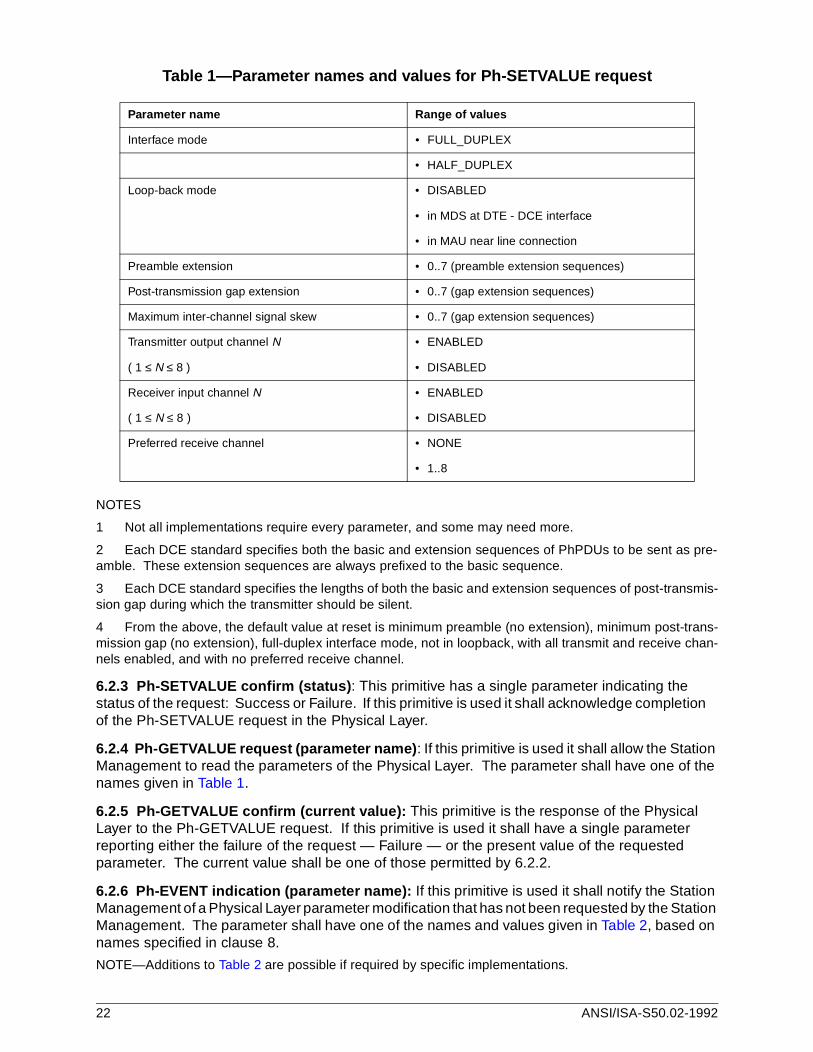
Table 1—Parameter names and values for Ph-SETVALUE request
NOTES
1 Not all implementations require every parameter, and some may need more.
2 Each DCE standard specifies both the basic and extension sequences of PhPDUs to be sent as pre-amble. These extension sequences are always prefixed to the basic sequence.
3 Each DCE standard specifies the lengths of both the basic and extension sequences of post-transmis-sion gap during which the transmitter should be silent.
4 From the above, the default value at reset is minimum preamble (no extension), minimum post-trans-mission gap (no extension), full-duplex interface mode, not in loopback, with all transmit and receive chan-nels enabled, and with no preferred receive channel.
6.2.3 Ph-SETVALUE confirm (status) : This primitive has a single parameter indicating the status of the request: Success or Failure. If this primitive is used it shall acknowledge completion of the Ph-SETVALUE request in the Physical Layer.
6.2.4 Ph-GETVALUE request (parameter name) : If this primitive is used it shall allow the Station Management to read the parameters of the Physical Layer. The parameter shall have one of the names given in Table 1.
6.2.5 Ph-GETVALUE confirm (current value): This primitive is the response of the Physical Layer to the Ph-GETVALUE request. If this primitive is used it shall have a single parameter reporting either the failure of the request — Failure — or the present value of the requested parameter. The current value shall be one of those permitted by 6.2.2.
6.2.6 Ph-EVENT indication (parameter name): If this primitive is used it shall notify the Station Management of a Physical Layer parameter modification that has not been requested by the Station Management. The parameter shall have one of the names and values given in Table 2, based on names specified in clause 8.
NOTE—Additions to Table 2 are possible if required by specific implementations.
Parameter name Range of values
Interface mode • FULL_DUPLEX
• HALF_DUPLEX
Loop-back mode • DISABLED
• in MDS at DTE - DCE interface
• in MAU near line connection
Preamble extension • 0..7 (preamble extension sequences)
Post-transmission gap extension • 0..7 (gap extension sequences)
Maximum inter-channel signal skew • 0..7 (gap extension sequences)
Transmitter output channel N • ENABLED
( 1 ≤ N ≤ 8 ) • DISABLED
Receiver input channel N • ENABLED
( 1 ≤ N ≤ 8 ) • DISABLED
Preferred receive channel • NONE
• 1..8
22 ANSI/ISA-S50.02-1992

Table 2—Parameter names for Ph-EVENT indication
7 DCE Independent Sublayer (DIS)
NOTES
1 The Physical Layer entity is partitioned into a Data Terminal Equipment (DTE) component and a DataCommunication Equipment (DCE) component. The DTE component interfaces with the Data Link Layerentity and forms the DCE Independent Sublayer (DIS). It exchanges Interface Data Units across the DL-Ph interface defined in clause 5, and provides the basic conversions between the PhIDU "at-a-time" view-point of the DL-Ph interface and the bit serial viewpoint required for physical transmission and reception.
2 This sublayer is independent of all the Physical Layer variations, including encoding and/or modulation,speed, voltage/current/optical mode, medium etc. All these variations are grouped under the designationData Communication Equipment (DCE).
The DIS shall sequence the transmission of the PhID as a sequence of serial PhSDUs. Similarly, the DIS shall form the PhID to be reported to the Data Link Layer from the sequence of received serial PhSDUs.
The PhID shall be converted to a sequence of PhSDUs for serial transmission in octets up to a maximum of 300 octets. A PhSDU representing more significant octets of the PhID shall be sent before or at the same time as a PhSDU representing less significant octets and such that within each octet, a PhSDU representing a more significant bit will be transmitted before or at the same time as a PhSDU representing a less significant bit. On reception, each sequence of PhSDUs shall be converted to PhID such that, in the absence of errors, the PhIDU indicated to the receiving Data Link Layer entity shall be unchanged from the PhIDU whose transmission was requested by the originating Data Link Layer entity.
3 This is a guarantee of transparency.
8 DTE-DCE interface
NOTES
1 The Physical Layer entity is partitioned into a Data Terminal Equipment (DTE) component containingthe MIS and higher layers and a Data Communication Equipment (DCE) component containing the MDSand lower sub-layers. The DTE-DCE interface connects these two physical components.
2 It is not mandatory for the DTE-DCE interface, or any other interface, to be exposed.
3 The DTE-DCE interface is a functional and electrical, but not mechanical, interface that supports a setof services. Each of these services is implemented by a sequence of defined signaling interactions at theinterface.
8.1 Services: The following services, defined in this sub-clause, shall be supported by the DTE-DCE interface:
a) DTE to DCE reset service;
Parameter name
DTE fault
DCE fault
ANSI/ISA-S50.02-1992 23

b) DTE to DCE configuration service;
c) DTE to DCE message transmission service;
d) DCE to DTE fault notification service;
e) DCE to DTE media-activity indication service;
f) DCE to DTE message reporting service.
8.1.1 DTE to DCE reset service: This service shall provide a means by which the DTE, at any time, can reset the DCE to its initial (power-on) state.
8.1.2 DTE to DCE configur ation service: This service shall provide a means by which the DTE can configure various characteristics of the DCE, including those characteristics that station man-agement can adjust via PhSETVALUE requests (see Table 1). It also shall provide a DCE-optional means by which the DTE can initiate reporting of DCE status by preemptive use of the DCE to DTE message reporting service.
8.1.3 DTE to DCE message transmission service: This service shall provide a means by which the DTE can transmit a message through the DCE to either the connected medium (media), or back to the DTE, or both, as determined by the current operational values of the parameters specified in Table 1. The DCE shall provide the pacing for this service.
This service is invoked upon receipt of a PhDATA request specifying START-OF-ACTIVITY at the PhL service interface and runs until receipt of and completion of the PhDATA request specifying END-OF-DATA-AND-ACTIVITY.
8.1.4 DCE to DTE faul t no tification service: This service shall provide a means by which the DCE, at any time, can report a fault. The specific nature of the fault is not reported by this service but may be determinable by use of the DTE to DCE configuration service to initiate a DCE-optional DCE status report.
8.1.5 DCE to DTE media-activity indi cation service: This service shall provide a means by which the DCE reports the inferred detection, on any of its connected media for which receiving is enabled (see Table 1), of signaling from itself or other Ph-layer entities. While loopback is enabled, this service reports only the signaling of the DCE itself.
When the DTE-DCE interface is in half-duplex mode and loopback is not enabled, this service need not report media activity resulting directly from the DTE to DCE message transmission service.
8.1.6 DCE to DTE message reporting service: This service shall provide a means by which the DCE reports the receipt of a sequence of PhPDUs from any one of the connected media for which receiving is enabled. This service terminates with an indication of whether the sequence of received PhPDUs was well formed. Errors in the sequence, including number of PhPDUs such that they could not have been a correct transmission resulting from an invocation of the DCE to DTE message transmission service shall be reported as a malformed (erroneous) sequence.
NOTE—Errors in the octet alignment of a received end delimiter with respect to the preceding start delimiter (i.e., not separated by an integral number of octets of data bits) is to be reported as a malformed sequence.
When the DTE-DCE interface is in half-duplex mode and loopback is not enabled, this service need not report the message transmitted by the DCE to DTE message transmission service.
8.2 Interface signals: If the DTE-DCE interface is exposed it shall provide the signals specified in Table 3.
24 ANSI/ISA-S50.02-1992

Table 3—Signals at DTE-DCE interface
The signal levels shall be as shown in Table 4. In general, both sides of the interface shall operate with the same approximate value of VDD. However, it is recognized that a DTE and a DCE with separate power supplies may not both reach operational VDD simultaneously. It is desirable, but not mandatory, that the DTE to DCE reset service be operational when the DCE has not yet reached operational VDD. It is also desirable that the DTE invoke this service whenever its own VDD is below operational margins.
Table 4—Signal levels for an exposed DTE-DCE interface
The timing characteristics of these signals shall be at least equal to those specified for the relevant DCE in the requirements of this part of ISA-S50.02. However, in no case shall the transition time between 0,3 VDD and 0,6 VDD be greater than either 100 ns or 0,025 P, whichever is smaller. P is defined as the nominal period of octet transmission—the inverse of the nominal PhSDU rate.
An implementation of the DTE-DCE interface shall function correctly with transmit and receive (TxC and RxC) clock frequencies between 1 kHz and 8,8 times the highest supported PhSDU rate of the DTE or DCE implementation.
NOTE—The PhSDU and equivalent bit data rates available in an implementation are stated in the Protocol Implementation Conformance Statement (PICS).
Signal Abbreviation Source
Transmit Clock TxC DCE
Request to Send RTS DTE
Clear to Send CTS DCE
Transmit Data TxD DTE
Receive Clock RxC DCE
Receive Activity RxA DCE
Receive Data and Framing RDF DCE
Symbol Parameter Conditions Limits Units Remarks
VOL Maximum low-level output voltage
Iout = ±100 µA
Iout = +1,6 mA
0,1
0,4
V
V
See Note 1
VOH Minimum high-level output voltage
Iout = ±100 µA
Iout = –0.8 mA
VDD - 0,1
VDD - 0,8
V
V
See Note 1
See Note 2
VIL Maximum low-level input voltage
0,2 VDD V
VIH Minimum high-level input voltage
0,7 VDD V See Note 3
NOTES:1) Provides the capability to drive two typical CMOS loads.2) CMOS input compatibility with TTL output requires a "pull-up" resistor from signal input to VDD.3) Compatible with CMOS output for 3,0 ≤ VDD ≤ 5,5 V. Compatibility with TTL output (4,75 V ≤ VDD ≤ 5,25 V)
requires a "pull-up" resistor from signal input to VDD.
ANSI/ISA-S50.02-1992 25
8.2.1 Transmit Clock (TxC): The Transmit Clock signal (TxC) shall provide the DTE with a continuous timing signal, such that any eight consecutive full cycles of this signal shall have the same octet period as the nominal transmit period for one data octet. The DCE shall source this nominally two-phase signal such that each phase has a duration of at least 0,04 P.
NOTE—This specification permits TxC to be a continuous, constant-period clock at the nominal bit rate (8 times the nominal octet rate) with a duty cycle of 32% to 68%, or for TxC to be a higher-frequency clock with some cycles omitted and with a duty cycle closer to 50%. This permits, for example, simple clocking in a DCE that recodes each 4 bits into 5 baud; the DCE could have a clock 10 times the nominal octet rate, with a duty cycle of between 40% and 60%, and would omit (the same) two cycles every octet.
TxC supports the DTE to DCE configuration and message transmission services.
8.2.2 Request to Send (RTS): The Request To Send (RTS) signal supports the DTE to DCE reset, configuration, and message transmission services. The DTE shall source this signal. The initial (power-on) and idle (no DTE to DCE service active) state of this signal shall be low.
When referenced to TxC at the DTE-DCE interface, this signal shall have a minimum setup time of the smaller of either 100 ns or 0,025 P; the hold time shall be zero or greater.
8.2.3 Clear to Send (CTS): The Clear to Send (CTS) signal supports the DTE to DCE configuration and message transmission services. The DCE shall source this signal. The initial (power-on) and idle (no DTE to DCE service active) state of this signal shall be low.
When referenced to TxC at the DTE-DCE interface, this signal shall have a minimum setup time of the smaller of either 100 ns or 0,025 P; the hold time shall be zero or greater.
8.2.4 Transmit Data (TxD): The Transmit Data (TxD) signal supports the DTE to DCE reset, configuration, and message transmission services. Binary data is transmitted from DTE to DCE during one phase of the latter two services, and during this phase a binary 0 is represented by a low level on TxD and a binary 1 by a high level on TxD, both sampled at the falling edge of TxC.
The DTE shall source this signal. The initial (power-on) and idle (no DTE to DCE service active) state of this signal shall be high.
When referenced to TxC at the DTE-DCE interface, this signal shall have a minimum setup time of the smaller of either 100 ns or 0,025 P; the hold time shall be zero or greater.
8.2.5 Receive Clock (RxC): The Receive Clock signal (RxC) shall provide the DTE with an intermittent (semicontinuous) nominally two-phase timing signal that defines the timing of informa-tion being reported via the RDF signal. The DCE shall source this signal such that, where RxC is defined to be meaningful (see 8.3.6), each phase has a duration of at least 0,04 P.
NOTE—This specification permits RxC to be a recovered clock at the nominal bit rate (8 times the nominal octet rate) with a duty cycle of 32% to 68%, or to be a higher-frequency clock with some cycles omitted and with a duty cycle closer to 50%. This permits, for example, simple clocking in a DCE that decodes 4 bits from each received 5 baud; the DCE could have a clock 10 times the nominal octet rate, with a duty cycle of between 40% and 60%, and would omit two cycles every octet.
This specification also permits the DCE to omit cycles of RxC during recognition of long end-delimiter sequences of PhPDUs, so that the delimiter can be reported in real time using 8 or fewer cycles of RxC (see 8.3.6).
RxC shall support the DCE to DTE message reporting service.
8.2.6 Receive Activity (RxA): The Receive Activity (RxA) signal shall support the DCE to DTE fault notification, media-activity indication, and message reporting services. The DCE shall source this signal. The initial (power-on) and idle (no DCE to DTE service active) state of this signal shall be low.
8.2.7 Receive Data and Framing (RDF): The Receive Data and Framing (RDF) signal shall
26 ANSI/ISA-S50.02-1992
support the DCE to DTE fault notification and message reporting services. Binary data is trans-mitted from DCE to DTE during some phases of the latter service, and during these phases a binary 0 is represented by a low level on RDF and a binary 1 by a high level on RDF, both sampled at the falling edge of RxC.
The DCE shall source this signal. The initial (power-on) and idle (no DCE to DTE service active) state of this signal shall be high.
When referenced to RxC at the DTE-DCE interface, this signal shall have a minimum setup time of the smaller of either 100 ns or 0,025 P; the hold time shall be zero or greater.
8.3 Encoding of services in signals: The services of 8.1 shall be implemented by the following sequences and combinations of the signals of 8.2.
NOTE—Typical transmit and receive sequencing machines are shown in Figure 3. Figure 3 is included in this part of ISA-S50.02 for explanatory purposes and does not imply a specific implementation.
ANSI/ISA-S50.02-1992 27

Figure 3—DTE/DCE sequencing machines
8.3.1 DTE to DCE reset service: This service shall be mutually exclusive with the DTE to DCE configuration and message transmission services; at most one of them may be active at any given time. This service may preempt the DTE to DCE configuration and message transmission services at any time.
This service shall be encoded as a simultaneous low level on both RTS and TxD. When asserted by the DTE, this simultaneous low level shall be held for at least the nominal transmission period of two PhSDUs (octets).
28 ANSI/ISA-S50.02-1992

NOTES
1 This is an asynchronous service and is not referenced to TxC.
2 When a DTE is itself being reset, possibly during power-up, it should attempt to reset the DCE evenwhen the DTE's own VDD is below normal operational limits.
3 This reset is under the control of the DTE. It does not preclude the existence of a separate reset pinon the DCE.
If the DTE concurrently changes both RTS and TxD during the implementation of either the DTE to DCE configuration or message transmission services, the DTE shall ensure that an interval of at least the minimum required setup time exists between changing the one signal to a high level, and subsequently changing the other signal to a low level, to eliminate potential logic hazards in the DCE's implementation of the DTE to DCE reset service.
8.3.2 DTE to DCE configuration service: This service is mutually exclusive with the DTE to DCE reset and message transmission services; at most one of them may be active at any given time. This service may initiate the DCE to DTE message reporting service to report DCE-internal status. The DTE to DCE reset service may preempt this service at any time.
This service shall be implemented in three phases; each of the latter two phases shall follow immediately upon completion of the prior phase.
NOTE 1—These phases can be implemented as a minor variation on the three phases specified for the DTE to DCE message transmission service. As a result, the DTE to DCE configuration service induces very little added complexity on the DTE and DCE.
1) The DTE shall assert (raise) RTS after the falling edge and before the rising edge of TxC. The DCE shall respond by anticipating configuration data.
2) When it is ready for configuration data from the DTE, the DCE shall raise CTS before the falling edge of TxC. The DTE shall respond by encoding the first bit of configuration data (high = 1, low = 0) on TxD before the falling edge of the next TxC, and shall continue this process without interruption until between 2 and 200 bits of data (see 8.4) have been so encoded. The DTE shall then assert (raise) TxD and negate (lower) RTS before the falling edge of the next TxC.
NOTE 2—The DTE shall ensure that TxD is raised at least one setup time before RTS is lowered to avoid potential logic hazards in the DCE implementation of the DTE to DCE reset service.
3) The DCE shall conclude any necessary reconfiguration before negating (lowering) CTS, which shall occur between two consecutive falling edges of TxC.
Both standardized and extendible configuration messages are defined in 8.4. Standardized messages cover the ranges of application of this interface which are anticipated to be most cost sensitive. Extendible messages permit differing forms of DCE configuration, where required, and can serve to initiate the DCE to DTE message reporting service to report DCE-internal status (a DCE option further described in 8.4).
8.3.3 DTE to DCE message transmission service: This service is mutually exclusive with the DTE to DCE reset and configuration services; at most one of them may be active at any given time. The DTE to DCE reset service may preempt this service at any time.
This service shall be implemented in three phases; each of the latter two phases shall follow immediately upon completion of the prior phase.
1) The DTE shall assert (raise) RTS after the rising edge and before the falling edge of TxC. The DCE shall respond by generating and transmitting the appropriate-length sequence of preamble and start delimiter PhPDUs.
ANSI/ISA-S50.02-1992 29

2) When it is ready for transparent data from the DTE, the DCE shall raise CTS before the falling edge of TxC. The DTE shall respond by encoding the first bit of transparent data (high = 1, low = 0) on TxD before the next falling edge of TxC and shall continue this process without interruption until between 3 and 300 integral octets of data have been so encoded. The DTE shall then assert (raise) TxD and negate (lower) RTS before the next falling edge of TxC.
NOTE—The DTE shall ensure that TxD is raised at least one setup time before RTS is lowered to avoid potential logic hazards in the DCE implementation of the DTE to DCE reset service.
3) The DCE shall conclude transmission of all of the encoded transparent data received from the DTE, shall then generate and transmit the appropriate length sequence of end delimiter PhPDUs and shall then cease transmission. The DCE shall then wait an amount of time equal to the configured minimum post-transmission gap (see Table 1) before negating (lowering) CTS, which shall occur after a falling edge and before the next falling edge of TxC.
8.3.4 DCE to DTE fault notification service: This service shall be mutually exclusive with the DCE to DTE media-activity indication and message reporting services; at most one of them may be active at any given time. This service may preempt the DCE to DTE media-activity indication and message reporting services at any time.
This service shall be encoded as a simultaneous low level on both RxA and RDF. Once asserted by the DCE, this simultaneous low level shall be held until activation of either the DTE to DCE reset or configuration services.
NOTE—This is an asynchronous service and is not referenced to RxC.
The DCE may concurrently change both RxA and RDF during the concurrent termination of the DCE to DTE media-activity indication and message reporting services. The DTE is responsible for avoiding any logic hazards induced by this concurrent change.
8.3.5 DCE to DTE media-activity indication service: This service is mutually exclusive with the DCE to DTE fault notification service; at most one of them may be active at any given time. The DCE to DTE fault notification service may preempt this service at any time.
This service shall be encoded as a high level on RxA. Once asserted by the DCE, this high level enables recognition of a high-to-low transition on RDF to initiate the DCE to DTE message reporting service. Any subsequent high-to-low transition on RxA terminates that DCE to DTE message reporting service.
NOTE—The DCE to DTE media-activity indication service is an asynchronous service and is not referenced to RxC.
8.3.6 DCE to DTE message reporting service: This service is mutually exclusive with the DCE to DTE fault notification service; at most one of them may be active at any given time. This service can only occur while the DCE to DTE media-activity indication service is active. The DCE to DTE fault notification service may preempt this service at any time.
8.3.6.1 Non-erroneous reception: This service shall be implemented in four phases when re-porting a well-formed message, each of which shall follow immediately upon completion of the prior phase.
The following description applies to DCEs that have end delimiter sequences of eight PhPDUs or less and do not require any extra decoding delay for an FEC (forward error correcting) code. DCEs that do not meet these conditions may introduce extra delay into their decoding and reporting processes so that, with respect to signaling on RxC and RDF, they do meet these conditions.
30 ANSI/ISA-S50.02-1992

1) After detecting received signaling, training on that signaling, and recovering a data clock from that signaling whose nominal octet frequency is the same as TxC, the DCE shall initiate the DCE to DTE message reporting service by sourcing that recovered clock on RxC and then negating (lowering) RDF after the rising edge and before the next falling edge of RxC.
NOTE 1—RxA is already asserted at this time.
2) The DCE shall continue training and attempting to match the received signaling against its expected preamble and start delimiter PhPDUs.
If the DCE supports N channels of redundant media, it may report on RDF the identityof the channel from which the signaling is being received by encoding that channelnumber, in the range 0 to N-1, as a binary number that is reported most significantbit first during reception of the last three of those start delimiter PhPDUs. The bitsreported on RDF shall be presented in series after successive rising edges of RxC,each before the immediately subsequent falling edge of RxC.
Upon detecting an exact match between the received signaling and the expectedstart delimiter, the DCE shall invert RDF after the falling edge and before the nextrising edge of RxC.
NOTE 2—If the identity of the receiving channel was being reported on RDF, this inversion will occur during the low phase of RxC that immediately follows the high phase (of RxC) during which the last (low-order) bit of the channel number was reported.
3) The DCE shall continue reception and attempting to match the received signaling against potential data and expected end delimiter PhPDUs.
The DCE shall report each data bit decoded from the received signaling on RDF. The bits reported on RDF shall be presented in series after successive rising edges of RxC, each before the immediately subsequent falling edge of RxC. In the absence of errors these bits shall be reported in the same order and with the same values as they were transmitted by a peer PhL entity.
NOTE 3—This is a guarantee of transparency.
An end delimiter may be composed of both data and non-data PhPDUs. The DCE may report similarly on RDF each data bit decoded from an end delimiter and may report also on RDF an appropriate number of data values for the non-data PhPDUs decoded from an end delimiter, except that
a) the total number of "bits" so reported shall be 7 or less, and
b) upon detecting an exact match between the received signaling and the expected end delimiter, the DCE shall not report on RDF another bit corresponding to the end delimiter's last "bit", but rather shall first assert (raise) RDF after the rising edge and before the next falling edge of RxC, and then shall negate (lower) RDF after the falling edge and before the next rising edge of RxC.
ANSI/ISA-S50.02-1992 31

NOTES
4 Most implementations will decode, and report on RDF as data, any initial data PhPDUs in a receivedend-delimiter sequence. The first non-data PhPDU, and subsequent PhPDUs, need not be reported. How-ever, a final report will be made on RDF, indicating correct end-delimiter recognition.
5 Each reported bit, except the last, is maintained on RDF for a full cycle of RxC. The last bit is replacedby a high-low sequence, each of which is maintained for just one phase of RxC.
6 This terminating high-low sequence will occur during the first eight "bit" reports that occur after the last(pre-delimiter) data bit was reported. That last (pre-delimiter) data bit will have been the 8Nth data bit soreported in this phase, where N should be at least 3 and no greater than 300.
4) The DCE shall assert (raise) RDF before the next falling edge of RxC and shall not initiate another instance of the DCE to DTE message reporting service until after the conclusion of the current DCE to DTE media-activity indication service.
8.3.6.2 Erroneous reception: An error may be detected during any phase of the reception process described in 8.3.6.1. When that occurs, the DCE shall modify its sequencing of those phases as follows.
If the DCE should detect invalid PhPDUs, or an invalid sequence of PhPDUs, or a valid end delimiter sequence of PhPDUs that is not separated from the start delimiter PhPDUs by an integral number of data-octets of PhPDUs; and if the DCE can establish a valid signal on RxC (for example, by substituting TxC or some other local signal for the recovered clock source, if necessary); then
a) if phase 2 has not already been initiated, the DCE shall immediately initiate phase 2;
b) if phase 2 has not already been concluded, the DCE shall immediately conclude phase 2 as rapidly as possible, ignoring the requirement for matching of the start delimiter PhPDU sequence;
c) otherwise, the DCE shall immediately negate (lower) RDF after the rising edge and before the next falling edge of RxC, and then shall assert (raise) RDF after the falling edge and before the next rising edge of RxC.
NOTE—This sequence permits the DCE to
— enable DTE use of RxC;
— identify the channel with the erroneous signaling; and
— indicate a reception error.
When the DCE has completed as many of the above steps (a), (b), and (c) as appropriate and possible, the DCE shall immediately initiate phase 4.
8.4 DCE configuration messages: This sub-clause defines both standardized configuration mes-sages and the standardized portion of extendible configuration messages. Standardized messages cover the ranges of application of this interface that are anticipated to be most commonly used. Extendible messages permit differing forms of DCE configuration where required and can serve to initiate the DCE to DTE message reporting service to report DCE-internal status (a DCE option).
Two standardized messages, and two classes of extendible messages, are defined. All messages are transmitted across the interface in the order in which the bits are defined. Integers are transmitted most-significant-bit (MSB) first.
The two standardized messages and two classes of extendible messages are distinguished by the first two data bits of the configuration message, as follows:
00—Basic configuration message01—Path-diversity control message10—Extendible configuration message11—Extendible status-report invocation message
32 ANSI/ISA-S50.02-1992

8.4.1 Basic configuration message: Following its initial two bits of (00), the basic configuration message specifies operational aspects common to most DCEs. The defined components of this message are, in order of transmission:
a) The operational mode of the DCE, encoded in one data bit as shown. The value for this parameter after activation of the DTE to DCE reset service is 0.
0 Two-way simultaneous (full-duplex), where each invocation of the DTE toDCE message transmission service automatically activates the DCE to DTEmedia-activity indication and message reporting services;
NOTE 1—This mode is desirable for dual-channel media such as fiber-optic pair cabling. Some DTEs may only be able to operate in this mode.
1 Two-way alternate (half-duplex), in which an invocation of the DTE to DCEmessage transmission service does not automatically activate the DCE to DTEmedia-activity indication and message reporting services;
NOTE 2—This mode minimizes DCE and DTE-DCE interface power consumption. Some DTEs may only be able to operate in this mode.
b) The selection of the DCE-internal data source for the message reporting service, encoded in two data bits as shown. (See Table 1.) The value for this parameter after activation of the DTE to DCE reset service is 00. When this selection is non-zero, transmission on all attached media shall be disabled and the DTE - DCE interface shall operate in two-way simultaneous (full-duplex) mode.
00 decoded signaling, received from one of the attached media as specified in8.4.2(b) and 8.4.2(c). The interface mode is as specified in 8.4.1(a).
01 internal-status reporting, see 8.4.4 and 8.5.
10 loopback as close as possible to the DTE-DCE interface, with no transmis-sion to connected media, where each invocation of the DTE to DCE messagetransmission service automatically activates the DCE to DTE media-activity in-dication and message reporting services;
NOTE 3—This mode is desirable for DCE vs. DTE vs. interconnect fault localization.
11 loopback as close as possible to the media interface(s), with no transmis-sion to connected media, where each invocation of the DTE to DCE messagetransmission service automatically activates the DCE to DTE media-activity in-dication and message reporting services.
NOTE 4—This mode is desirable for self-assessment before entry to an operating network.
c) The amount by which the preamble, which is the initial sequence of PhPDUs in each transmission, should be extended. Its range is zero to seven units of extension, encoded in three data bits as 0 (000) to 7 (111). The value for this parameter after activation of the DTE to DCE reset service is 0 (000). (See note 2 of 6.2.3.)
d) The amount by which the mandatory post-transmission gap, which is the period of nontransmission between successive sequences of PhPDUs, should be extended. Its range is zero to seven units of extension, encoded in three data bits as 0 (000) to 7 (111). The value for this parameter after activation of the DTE to DCE reset service is 0 (000). (See note 3 of 6.2.3.)
ANSI/ISA-S50.02-1992 33

8.4.2 Path-diversity control message: Following its initial two bits of (01), the path-diversity control message specifies additional configuration data commonly required for management and fault-assessment of redundant paths: separate transmission and reception controls for each of the attached redundant media (channels and paths). The defined components of this message are, in order of transmission:
a) Two bits of zero (00), which provide quartet and octet alignment within the message for the following fields.
b) The algorithm for choosing between redundant media as the source of received signaling when more than one of the media is enabled for reception, coded in four bits as shown. The value for this parameter after activation of the DTE to DCE reset service is 0000.
0000—The medium selected for reception should be the first medium on which signal-ing that is suitable for receiver-training is detected.
1000 to 1111 (= 7 + N, 1 ≤ N ≤ 8)—The Nth medium should be selected, except whensignaling suitable for receiver-training has been detected on another medium for a pe-riod of time equal to the extra period of inter-frame-gap extension specified in 8.4.1(d),in which case that other medium should be selected.
c) The selection of whether reception is enabled (0) or inhibited (1) on each of eight or fewer redundant media, coded in eight consecutive bits for channels 1 through 8, respectively. (See Table 1.) The value for this parameter after activation of the DTE to DCE reset service is 0000 0000.
d) The selection of whether transmission is enabled (0) or inhibited (1) on each of eight or fewer redundant media, coded in eight consecutive bits for channels 1 through 8, respectively. (See Table 1.) The value for this parameter after activation of the DTE to DCE reset service is 0000 0000.
e) The amount of post-transmission gap extension due to potential signal skew between redundant media. Its range is zero to seven units of extension, encoded in three data bits as 0 (000) to 7 (111). The value for this parameter after activation of the DTE to DCE reset service is 0 (000). (See 8.4.1(d), 8.4.2(b), and note 3 of 6.2.2.)
8.4.3 Extend ible con figur ation messages: Following its initial two bits of (10), the coding of extendible configuration messages may be implementation dependent. The structure and form of extendible configuration messages shall be the same as the basic configuration message specified in 8.4.1.
8.4.4 Extendible status-report invocation messages: Following its initial two bits of (11), the coding of extendible status-report invocation messages may be implementation dependent. The structure and form of extendible status-report invocation messages shall be the same as the basic configuration message specified in 8.4.1. The information specified shall select some DCE-internal source of received signaling, and if the DCE-internal-data-source mode is status-reporting (see 8.4.1(b)), the DCE shall generate a multi-data-octet message, padded as necessary to an octet multiple and shall report it using the DCE to DTE media-activity indication and message reporting services.
8.5 DCE-generated status reports: These reports are generated within the DCE upon request and reported when the DCE-internal-data-source is internal-status report. (See 8.4.1(b)).
34 ANSI/ISA-S50.02-1992

9 Medium Dependent Sublayer (MDS): Wire media
NOTE—The Medium Dependent Sublayer (MDS) is part of the Data Communication Equipment (DCE). It exchanges serial PhSDU sequences across the DTE-DCE interface specified in clause 8 and it communi-cates encoded bits across the MDS-MAU interface specified in Clause 10. The MDS functions are logical encoding and decoding for transmission and reception, respectively, and the addition/removal of preamble and delimiters together with timing and synchronization functions.
9.1 PhPDU: The MDS shall produce the PhPDU shown in Figure 4 by adding preamble and delimiters to frame the serial sequence of PhSDUs (bits) transferred from the DIS across the DTE-DCE interface. Transmission sequence shall be from left to right as shown in Figure 4, i.e., preamble first, followed by start delimiter, PhSDU sequence, and end delimiter.
Figure 4—Protocol Data Uni t (PhPDU)
Conversely, the MDS shall remove preamble and delimiters from a received PhPDU to produce a corresponding serial sequence of PhSDUs. If a nonbinary data unit is detected in the received PhSDU sequence, the MDS shall immediately stop transferring PhSDUs to the DIS, the MDS shall report an error, and the MDS shall indicate the end of activity to the DIS when it happens.
9.2 Encoding and d ecoding : Data units shall be encoded by the MDS for application to the MAU using the code shown in Figure 5 (Manchester Biphase L). The encoding rules are formally given in Figure 6 and Table 5.
Figure 5—PhSDU encoding and decodingNOTE 1—Figure 5 is included in this part of ISA-S50.02 for explanatory purposes and does not imply a specific implementation.
ANSI/ISA-S50.02-1992 35

Figure 6—Encoding rules
Table 5—Encoding rules
NOTE 2—It may be seen that data symbols (1 and 0, conveyed by PhSDUs) are encoded to always contain a mid-bit transition. Non-data symbols (N+ and N–) are encoded so that they never have a mid-bit transition. Frame delimiters (see 9.4 and 9.5) are constructed so that non-data symbols are conveyed in pairs of opposite polarity.
Decoding shall normally be the opposite of encoding. At reception, the MDS shall verify that each symbol is encoded in accordance with Figure 6 and Table 5 and shall detect the following errors:
a) invalid Manchester code;
b) half-bit-slip errors.
Any of these errors shall be reported as Ph-DATA indication (PhIDU, error).
9.3 Polarity detection: The option of automatic polarity detection of the received Manchester encoded signal shall be required where it is specified in the relevant MAU.
9.4 Start of frame delimiter: The following sequence of symbols, shown from left to right in order of transmission, shall immediately precede the PhSDU sequence to delimit the start of a frame:
1, N+, N–, 1, 0, N–, N+, 0.
(shown as a waveform in Figure 7)
Symbols Encoding
1 (ONE) Hi-Lo transition (mid-bit)
0 (ZERO) Lo-Hi transition (mid-bit)
N+ (NON-DATA PLUS) Hi (No transition)
N- (NON-DATA MINUS) Lo (No transition)
36 ANSI/ISA-S50.02-1992

The MDS shall only accept a received signal burst as a PhPDU after verifying this sequence and shall remove this sequence before transferring the PhSDU sequence to the DIS.
9.5 End of frame delimiter: The following sequence of symbols, shown from left to right in order of transmission, shall immediately follow the PhSDU sequence to delimit the end of a frame:
1, N+, N–, N+, N–, 1, 0, 1.
(shown as a waveform in Figure 7)
The MDS shall remove this sequence from the PhPDU before transferring the PhSDU sequence to the DIS. The MDS shall report to the corresponding Data Link Layer entity any frames received via the medium that do not include this sequence within 300 octets of start of frame (from beginning of start delimiter) as Ph-DATA indication (PhIDU, frame_too_long). The MDS shall report to the corresponding Data Link Layer entity, via the corresponding DIS, any frames received via the medium that have an end delimiter that is not located at an octet boundary as Ph-DATA indication (PhIDU, received_timing_error).
9.6 Preamble: In order to synchronize bit times a preamble shall be transmitted at the beginning of each PhPDU consisting of the following sequence of bits, shown from left to right in order of transmission:
1, 0, 1, 0, 1, 0, 1, 0.
(shown as a waveform in Figure 7)
NOTE—Received preamble can contain as few as four bits due to loss of one bit through each of four repeaters (as specified in the MAU Network Configuration Rules).
The period may be extended, but not reduced, by Station Management as given in Table 1. A preamble extension sequence as listed in Table 1 shall be defined as the following sequence of bits, shown from left to right in order of transmission:
1, 0, 1, 0, 1, 0, 1, 0.
9.7 Synchronization: After the reception of the fourth bit of the frame and until end of frame or frame termination, the receiver shall detect and report half-bit-slip errors.
NOTE 1—This synchronization specification allows the loss of four bits of the preamble.
After the preamble, half-bit-slip errors shall be reported as Ph-DATA indication (PhIDU, error).
NOTE 2—Half-bit-slip errors can be detected as excessive bit cell jitter and/or excessive variation in bit period.
ANSI/ISA-S50.02-1992 37

Figure 7—Preamble and delimitersNOTE—These waveforms do not extend the frequency range outside the band required for transmission of binary PhSDUs (conveying data symbols) in accordance with Figure 6 and Table 5.
9.8 Post-transmission gap: After transmission of a PhPDU, there shall be a minimum period during which a subsequent transmission shall not commence. For the same minimum period after reception of a PhPDU, the receiving Physical Layer entity shall ignore all received signaling. An MDS entity shall set a minimum post transmission period of four nominal bit times. The period may be extended, but not reduced, by Station Management as given in Table 1 or by an associated MAU entity. A gap extension sequence as listed in Table 1 shall be defined as four nominal bit times.
NOTE—The MAU transmit enable/disable time may reduce the duration of silence between frames.
9.9 Interchannel signal skew: If the device is configured (by Station Management) to receive concurrently on more than one channel then the maximum accepted differential delay between any two active channels, as measured from the first PhPDU of a start delimiter, shall not exceed five nominal bit times. This period may be extended, but not reduced, by Station Management as given in Table 1. A gap extension sequence as listed in Table 1 shall be defined as four nominal bit times. The value of post-transmission gap shall be greater than the value of interchannel skew.
38 ANSI/ISA-S50.02-1992

10 MDS - MAU interface: Wire media
NOTE—The Medium Attachment Unit (MAU) is an optionally separate part of a communication element which connects to the medium directly or via passive components. For electrical signaling variants the MAU is the transceiver, which provides level shifting and wave shaping for transmitted and received signals. The MDS - MAU interface links the MAU to the MDS. The services are defined as physical signals to facilitate this interface being optionally exposed. Table 6 lists the minimum set of required services at the MDS-MAU interface. See clause 6 for management services.
10.1 Services: If the MDS-MAU interface is exposed, it shall support at least the set of required services given in Table 6 and specified in 10.2.
Table 6—Minimum services at MDS-MAU interface
10.2 Service specifications
10.2.1 Transmit Signal (TxS): The Transmit Signal service (TxS) shall transfer the encoded PhPDU signal sequence across the MDS-MAU interface to the MAU, where the sequence shall be transmitted onto the medium if the Transmit Enable (TxE) is set to logic 1 (high level).
10.2.2 Receive Signal (RxS): The Receive Signal service (RxS) shall transfer the encoded PhPDU signal sequence or silence across the MAU-MDS interface to the MDS. The RxS shall echo the signal transmitted via TxS by simultaneously receiving the transmissions from the medium.
10.2.3 Transmit Enable (TxE): The Transmit Enable service (TxE) shall provide the MDS with the facility to enable the MAU to transmit. The TxE shall be set to logic 1 (high level) at the commencement of preamble transmission and then set to logic 0 (low level) after the last bit of the end delimiter has been transmitted.
If redundant media are in use and the method of implementing redundancy is to receive on all channels but transmit on only one, then the channel (cable) that is currently used for transmission shall be selected by setting its TxE to logic 1 (high level). All channels that are not currently in use for transmission shall be disabled by setting the TxE to logic 0 (low level).
10.2.4 Loopback Enable (LbE): If the optional Loopback Enable (LbE) service shown in Table 1 is used, it shall disable the final output stage of the MAU transmit circuit, connect the output of the previous stage of the MAU transmit circuit to the MAU receive circuit, and disconnect the MAU receive circuit from the medium. The state of the Loopback Enable shall not change while the MAU is transmitting or receiving.
Service Abbreviation Direction
Required:
Transmit Sig-nal
TxS To MAU
Receive Signal RxS From MAU
Transmit En-able
TxE To MAU
Optional:
Loopback enable LbE To MAU
ANSI/ISA-S50.02-1992 39

NOTE—This is confirmation service of local significance only, which provides a device with the facility to test the integrity and functionality of the Physical Layer circuitry, excluding the medium.
10.3 Signal characteristics: Timing characteristics shall be compatible with those specified in the requirements of this part of ISA-S50.02 for the relevant MDS.
If the MDS-MAU interface is exposed it shall operate with digital signal levels as shown in Table 7. Both sides of the interface shall operate with the same value of VDD.
Table 7—Signal levels for an exposed MDS-MAU interface
10.4 Communication mode: The communication mode at this interface shall allow simultaneous transmission and reception.
10.5 Timing characteristics: The MDS-MAU interface shall function correctly with a PhSDU bit rate of between 1 kbit/s and 1,1 times the highest stated MAU bit rate.
NOTE—The bit rates available in an implementation are stated in the Protocol Implementation Conformance Statement (PICS).
Symbol Parameter Conditions Limits Units Remarks
VOL Maximum low-level output voltage
Iout = ±100 µA
Iout = +1,6 mA
0,1
0,4
V
V
See Note 1
VOH Minimum high-level output voltage
Iout = ±100 µA
Iout = –0,8 mA
VDD – 0,1
VDD – 0,8
V
V
See Note 1
See Note 2
VIL Maximum low-level input voltage
0,2 VDD V
VIH Minimum high-level input voltage
0,7 VDD V See Note 3
NOTES:1) Provides the capability to drive two typical CMOS loads.2) CMOS input compatibility with TTL output requires a “pull-up” resistor from signal input to VDD.3) Compatible with CMOS output for 3,0 ≤ VDD ≤ 5,5 V. Compatibility with TTL output (4,75 V ≤ VDD ≤ 5,25 V) requires a “pull-up” resistor from signal input to VDD.
40 ANSI/ISA-S50.02-1992

11 Medium Attachment Unit (MAU): 31,25 kbit/s, voltage mode, wire medium
NOTES
1 The 31,25 kbit/s voltage-mode MAU simultaneously provides access to a communication network andto an optional power distribution network. Devices attached to the network communicate via the mediumand may or may not be powered from it. If bus powered, power is distributed as direct voltage and current,and communications signals are superimposed on the DC power. In intrinsically safe applications, availablepower may limit the number of devices.
2 The network medium consists of twisted pair cable. Independent of topology, all attached devices, oth-er than possibly the transmitting device, are high impedance to prevent significant network loading. Trap-ezoidal waveforms are used to reduce electromagnetic emissions.
3 Bus and tree topologies are supported. In either topology a network contains one trunk cable, termi-nated at both ends. In the bus topology, spurs are distributed along the length of the trunk. In the tree to-pology, spurs are concentrated at one end of the trunk. A spur may connect more than one device to thenetwork, the number of devices depending on spur length.
4 At the power frequency (DC), devices appear to the network as current sinks, with a limited rate ofchange of the supply current drawn from the medium. This prevents transient changes in load current frominterfering with communication signals.
11.1 Transmitted bit rate: The transmitted bit rate shall be 31,25 kbit/s ± 0,2%, averaged over a frame having a minimum length of 16 octets. The instantaneous bit time shall be 32 µs ± 0,9 µs.
11.2 Network specifications:
NOTE—A 31,25 kbit/s voltage-mode MAU operates in a network composed of the following components:
a) cable;
b) terminators;
c) couplers;
d) devices (containing at least one communication element).
A wire network in 31,25 kbit/s voltage mode may optionally include the following components:
e) connectors;
f) power supplies;
g) devices that include power supplies;
h) intrinsic safety barriers.
11.2.1 Topologies: A wire MAU shall operate in a network with a linear bus topology, consisting of a trunk, terminated at each end as specified in 11.7.5, to which communication elements are connected via couplers and spurs.
NOTES
1 The coupler and communication element may be integrated in one device (i.e., zero length spur).
2 Tree topology with all the communication elements located at the ends of the trunk is regarded as aspecial case of a bus for the purpose of this part of ISA-S50.02.
3 Several communication elements may be connected to the trunk at one point using a multi-port cou-pler. An active coupler may be used to extend a spur to a length that requires termination to avoid reflec-tions and distortions. Active repeaters may be used to extend the length of the trunk beyond that of a singlesegment as permitted by the network configuration rules.
ANSI/ISA-S50.02-1992 41

11.2.2 Network configuration rules: A 31,25 kbit/s voltage-mode MAU shall be required to conform to the requirements of this part of ISA-S50.02 when used in a network that complies with these rules.
Rule 1: One fieldbus shall be capable of communication between the following numbers of devices, all operating at the same bit rate:
a) between two and 32 devices for a non-I.S. fieldbus without power supplied via the signal conductors;
b) between two and six bus powered devices for an I.S. fieldbus, of which between one and four shall be in the hazardous area;
c) between one and 12 bus powered devices at the remote end from the power supply communicating with one device at the power supply end, for a non-I.S. fieldbus with power supplied via the signal conductors.
NOTE 1—Rule 1 does not preclude the use of more than the specified number of devices in an installed system. The numbers of devices were calculated on the assumption that a bus powered device draws 9 mA ± 1 mA. Item b) assumes that the I.S. barrier operates with a 19 V DC output and provides 40 to 60 mA to the devices in the hazardous area. Item c) assumes that the minimum power supply voltage is 20 V DC.
Rule 2: A fully loaded (maximum number of connected devices) 31,25 kbit/s voltage-mode fieldbus segment shall have a total cable length, including spurs, between any two devices, of up to 1 900 m.
NOTE 2—1 900 m maximum cable length is the requirement for conformance to this part of ISA-S50.02, but this does not preclude the use of longer lengths in an installed system.
Rule 3: The total number of waveform regenerations by repeaters and active couplers between any two devices shall not exceed four.
Rule 4: The maximum propagation delay between any two devices shall not exceed 20 nominal bit times.
NOTE 3—For efficiency of the network, that part of the turnaround time of any device on the network caused by a PhE between the end of a received frame and the beginning of the transmitted frame containing an associated immediate response should not exceed 5 bit times, no more than 2 bit times of which should be due to the MAU. As it is not mandatory to expose the DLL-PhL interface or the MDS-MAU interface, that part of the turnaround time of a fieldbus device caused by the PhL or the MAU cannot be specified or conformance tested.
Rule 5: The fieldbus shall be capable of continued operation while a device is being connected or disconnected. Data errors induced during connection or disconnection shall be detected.
Rule 6: Failure of any communication element or spur (with the exception of a short circuit, low impedance, or jabber) shall not interfere with transactions between other communication elements for more than 1 ms.
Rule 7: In polarity sensitive systems the medium twisted pairs shall have distinctly marked conductors that uniquely identify individual conductors. The polarization shall be maintained at all connection points.
Rule 8: The degradation of the electrical characteristics of the signal, between any two devices, due to attenuation, attenuation distortion, and mismatching shall be limited to the values indicated below.
a) Signal attenuation: The configuration of the bus (trunk and spur lengths, number of devices, I.S. barriers, galvanic isolators, and possible matching devices) shall be such that the attenuation between any two devices at the frequency corresponding to the bit rate shall not exceed 10,5 dB.
42 ANSI/ISA-S50.02-1992

b) Attenuation distortion: The configuration of the bus (trunk and spur lengths and number of devices, I.S. barriers, and galvanic isolators) shall be such that between any two devices:
[Attenuation (1,25 fr) – Attenuation (0,25 fr)] d 6 dB
Attenuation (1,25 fr) t Attenuation (0,25 fr)
where fr is the frequency corresponding to the bit rate. Attenuation shall be mono-tonic for all frequencies from 0,25 fr to 1,25 fr (7,8 kHz to 39 kHz).
c) Mismatching Distortion: Mismatching (due to spurs or any other effect, including one open circuit spur of maximum length) on the bus shall be such that, at any point along the trunk, in the frequency band 0,25 fr to 1,25 fr (7,8 kHz to 39 kHz):
|(Z – Z0) / (Z + Z0)| d 0,2
where Z0 is the characteristic impedance of the trunk cable and Z is the parallelcombination of Z0 and the load impedance at the coupler.
The concentration of couplers shall be less than 15 per 250 m.
NOTE 4—Rule 8 minimizes restrictions on trunk and spur length, number of devices, etc., by specifying only the transmission limitations imposed by combinations of these factors. Different combinations may be used depending on the needs of the application.
Rule 9: The following rules shall apply to systems implemented with redundant media:
a) each channel (cable) shall comply with the network configuration rules;
b) there shall not be a nonredundant segment between two redundant segments;
c) repeaters shall also be redundant;
d) if the system is configured (by Station Management) to transmit on more than one channel simultaneously, the propagation time difference between any two devices on any two channels shall not exceed five bit times;
e) channel numbers shall be maintained throughout the fieldbus, i.e., channels 1, 2, 3... from Station Management shall always connect to physical channels 1, 2, 3...
11.2.3 Power distribution rules for network configuration: The cable shield shall not be used as a power conductor.
11.3 Transmit circuit specification for 31,25 kbit/s voltage-mode MAU:
NOTE—For ease of reference, the requirements of 11.1 and 11.3 are summarized in Tables 8 and 9.
ANSI/ISA-S50.02-1992 43

Table 8—Transmit level specification summary for 31,25 kbit/s voltage-mode MAU
Table 9—Transmit timing specification summary for 31,25 kbit/s voltage-mode MAU
11.3.1 Test configuration: Figure 8 shows the configuration that shall be used for testing.
Figure 8—Transmit circuit test configurationDifferential signal voltage: Vd = Va – Vb
Test load resistance R = 50 Ω (0,5 cable Z0) and C = 10 µF except where otherwise stated in a specific requirement.
Transmit level characteristics, values referred to trunk (but measured using test load as shown in Figure 8 )
Limits for 31,25 kbit/s (bus-powered and/or I.S.)
Output level (peak-to-peak, see Figure 9)With test load (0,5 nominal Z0 of trunk cable)
0,75 V to 1 V50 Ω ± 1%
Maximum positive and negative amplitude difference (signaling bias) as shown in Figure 10
± 50 mV
Output Level; with one terminator removed (peak-to-peak); With test load (nominal Z0 of trunk cable)
d 2,0 ς 100 Ω ± 1%
Output Level; open circuit, (peak-to-peak)
d 3,0 V
Maximum output signal distortion; i.e., overvoltage, ringing and droop, (See Figure 9)
± 10%
Quiescent transmitter output; i.e., transmitter noise, (measured over the frequency band 1 kHz to 100 kHz)
d 1 mV (rms)
Transmit timing characteristics, values referred to trunk (but measured using test load as shown in Figure 8 )
Limits for 31,25 kbit/s (bus-powered and/or I.S.)
Transmitted bit rate 31,25 kbit/s ± 0,2%
Instantaneous bit time 32 µs ± 0,9 s
Rise and fall times (10% to 90% of pk-pk signal, see Figure 9) ± 0,25 nominal bit time
Slew rate (at any point from 10% to 90% of pk-pk signal) ± 0,2 V/µs
Maximum transmitted bit cell jitter (zero-crossing point deviation, see Figure 10)
± 0,025 nominal bit time
Transmit enable/disable time (i.e., time during which the output waveform may not meet the transmit requirements)
d 2,0 nominal bit times
44 ANSI/ISA-S50.02-1992

11.3.2 Output level requirements:
NOTE—Figure 9 shows an example of the AC component of one cycle of a fieldbus waveform, illustrating some key items from the transmit circuit specification. Only signal voltages are shown; this diagram takes no account of power supply voltages.
Figure 9—Output waveform
A 31,25 kbit/s MAU transmit circuit shall conform to the following output level requirements, all amplitudes being measured at the estimated midpoint between any peaks or troughs in the top and bottom of the waveform ("midpoint" in Figure 9):
a) the output voltage across the test load after transformer step up/down (if applicable) shall be between 0,75 V and 1,0 V peak-to-peak, with a load resistance of 50 Ω ± 1% ("min o/p" in Figure 9);
b) the output voltage at the trunk, or at the transmit terminals, with a load resistance of 100 Ω (i.e., with one trunk terminator removed) shall not exceed 2,0 V peak-to-peak ("max o/p one terminator removed" in Figure 9);
c) the output voltage at the trunk, or at the transmit terminals, with any load including an open circuit shall not exceed 3,0 V peak-to-peak. For test purposes open circuit shall be defined as a load of 100 kΩ resistance in parallel with 15 pF capacitance;
d) during transmission a device shall not suffer permanent failure when a load resistance of d 1 Ω is applied for 1 second;
e) the difference between positive amplitude and negative amplitude, measured as shown in Figure 10, shall not exceed ± 50 mV peak;
f) the output noise from a 31,25 kbit/s voltage-mode MAU that is receiving or not powered shall not exceed 1 mV rms, measured differentially over a frequency band of 1 kHz to 100 kHz, referred to the trunk;
g) the differential voltage across the test load shall be such that the voltage monotonically changes between 10% and 90% of peak-to-peak value. Thereafter, the signal voltage shall not vary more than ± 10% of peak-to-peak value until next transition occurs. This permitted variation shall include all forms of output signal distortion, i.e., overvoltage, ringing, and droop.
ANSI/ISA-S50.02-1992 45

11.3.3 Output timing requirements: A 31,25 kbit/s MAU transmit circuit shall conform to the following output timing requirements:
a) rise and fall times, measured from 10% to 90% of the peak-to-peak signal amplitude shall not exceed 0,25 nominal bit time (see Figure 9);
b) slew rate shall not exceed 0,2 V/µs measured at any point in the range 10% to 90% of the peak-to-peak signal amplitude (see Figure 9);
NOTE—Requirements a) and b) produce a trapezoidal waveform at the transmit circuit output. Requirement b) limits the level of interference emissions that may be coupled to adjacent circuits, etc. Requirement b) is calculated from the formula:
max. slew rate = 2 x min. slew rate = 2 x 0,8 V0 / 0,25 T = 6,4 x V0 / T
where V0 is the maximum pk-pk output voltage with standard load (1,0 V), and T is the nominal bit time (32 s).
c) transmitted bit cell jitter shall not exceed ±0,025 nominal bit time from the ideal zero crossing point, measured with respect to the previous zero crossing (see Figure 10);
Figure 10—Transmitted bit cell jitter (zero crossing point deviation)
d) the transmit circuit shall turn on, i.e., the signal shall rise from below the transmit circuit maximum output noise level as specified in 11.3.2 f) to full output level, in less than 2 nominal bit times. The waveform corresponding to the third and later bit times shall be as specified by other parts of 11.3;
e) the transmit circuit shall turn off, i.e., the signal shall fall from full output level to below the transmit circuit maximum output noise level as specified in 11.3.2 f), in less than 2 nominal bit times. The time for the transmit circuit to return to its off state impedance shall not exceed 4 nominal bit times. For the purposes of testing, this requirement shall be met with the transmit circuit test configuration of 11.3.1 with the equivalent capacitance of a maximum length cable across the DUT terminals.
NOTE—This requirement is to ensure that the transition of the transmit circuit from active to passive leaves the line capacitance fully discharged.
46 ANSI/ISA-S50.02-1992

11.4 Receive circuit specification for 31,25 kbit/s voltage-mode MAU:
NOTE—For ease of reference, the requirements of 11.4 are summarized in Table 10.
Table 10—Receive circuit specification summary for 31,25 kbit/s voltage-mode MAU
11.4.1 Input impedance: The differential input impedance of a 31,25 kbit/s voltage-mode MAU receive circuit shall be no less than 3 kΩ over the frequency range 0,25 fr to 1,25 fr (7,8 kHz to 39 kHz). This requirement shall apply after a 10 ms start-up time following connection to the network or application of power to the network. Independently powered devices (or network-powered devices capable of being turned off while connected to the network) shall meet this requirement in the power-on and power-off states and in transition between these states. This impedance shall be measured at the communication element terminals using a sine wave with a signal amplitude greater than the receiver sensitivity threshold and lower than 2,0 V peak-to-peak.
NOTES
1 The requirement for t 3 kΩ input impedance during power-up and power-down may be met by automatic disabling of the transmitter during these periods.
2 Devices with fault disconnection electronic circuits can have impedances less than the specified amount under fault conditions.
11.4.2 Receiver sensitivity and noise rejection: A 31,25 kbit/s voltage-mode MAU receive circuit shall be capable of accepting an input signal of amplitude no less than 150 mV peak-to-peak, including overvoltage and oscillation (see "signal level" in Figure 11 together with "positive ampli-tude" and "negative amplitude" in Figure 9).
A 31,25 kbit/s voltage-mode MAU receive circuit shall not respond to an input signal with a peak-to-peak amplitude that does not exceed 75 mV (see "noise rejection" in Figure 11).
Figure 11—Receiver sensitivity and noise rejection
Receive circuit characteristics(values referred to trunk)
Limits for 31,25 kbit/s
Input impedance, measured over the frequency range 0,25 fr to 1,25 fr t 3 kΩ
Sensitivity; min. pk-pk signal required to be accepted (see Figure 11)
150 mV
Noise rejection; max. pk-pk noise required to be rejected (see Figure 11)
75 mV
Maximum received bit cell jitter; (zero-crossing point deviation, see Figure 12)
± 0,10 nominal bit time
ANSI/ISA-S50.02-1992 47

11.4.3 Interference susceptibility and error rates:
NOTE 1—When the fieldbus is operating in a variety of standard noise environments the probability that an Application Layer User Data Unit contains an undetected error, due to operation of the conveying Physical and Data Link Layer entities, should be less than 1 in 6 x 10⁹ (1 error in 20 years at 10 messages/s). A communication element is regarded as conforming to this theoretical requirement when it meets the following interference susceptibility requirements. These are specified by a detected frame error rate, which is derived by using a ratio of detected to undetected errors of 106. This follows the IEEE 802 Functional Requirements Document, Draft 5.9, sections 5.6.1 and 5.6.2, and should be readily achievable with a 16-bit Frame Check Sequence at the Data Link Layer.
A communication element that includes a 31,25 kbit/s voltage-mode MAU, operating with frames containing 32 random user data bits, with maximum frame rate, and with signals of 375 mV pk-pk amplitude shall produce no more than 10 detected frame errors in 60 000 frames during operation in the presence of common mode voltage or Gaussian noise as follows:
a) a common mode sinusoidal signal of any frequency from 63 Hz to 2 MHz, with an amplitude of 4 V rms and from 47 Hz to 63 Hz with an amplitude of 250 V rms;
b) a common mode DC signal of ± 10 V;
c) white Gaussian additive differential noise in the frequency band 1 kHz to 100 kHz, with a noise density of 70 µV/
NOTE 2—The common mode voltage and Gaussian noise specifications are for receive circuit conformance testing with balanced loads and are not indicative of system installation practice.
A communication element that includes a 31,25 kbit/s voltage-mode MAU, operating with frames containing 32 random user data bits, at an average of 10 messages per second, with signals of 375 mV pk-pk amplitude shall produce no more than 10 detected frame errors in 1 000 frames during operation in the presence of electromagnetic or electrical interference environments as follows:
1) 10 V/m electromagnetic field as specified in IEC 801-3 at severity level 3;
2) electrical fast transient as specified in IEC 801-4 at severity level 3.
The above error rate specification shall also be satisfied after but not during operation in the following noise environments:
1) 8 kV electrostatic discharge to exposed metalwork as specified in IEC 801-2 at severity level 3. If the device suffers temporary loss of function or performance as a result of this test it shall recover from any such loss without operator intervention within 3 seconds after the end of the test;
2) high frequency disturbance tests as specified in IEC 255-4 Appendix E, Test voltage class III (2,5 kV and 1 kV peak values of first half-cycle in longitudinal and transverse mode, respectively). If the device suffers temporary loss of function or performance as a result of this test, it shall recover from any such loss without operator intervention within 3 seconds after the end of the test.
11.4.4 Received bit cell jitter : The receive circuit shall accept a Manchester encoded signal transmitted in accordance with 11.1 and 11.3. In addition, the receiver shall work properly with signals with the time variation between any two adjacent signal transition points (zero crossing) of ± 0,10 nominal bit time or less. See Figure 12.
NOTES
1 This does not preclude the use of receivers that perform better than this specification.2 Depending on the symbol pattern, the nominal time between zero crossings may be one-half or one bittime.3 There is no requirement to reject a signal with a specified time variation value. The receiver reports anerror when the received bit cell jitter exceeds the receiver's ability to reliably decode signaling.
Hz rms
48 ANSI/ISA-S50.02-1992

Figure 12—Received bit cell jitter
11.5 Jabber inhibit: The MAU shall contain a self-interrupt capability to inhibit transmitted signals from reaching the medium. Hardware within the MAU (with no external message other than the detection of output signals or leakage via the transmit function) shall provide a window of between 120 ms and 240 ms, during which time a normal frame may be transmitted. If the frame length exceeds this duration, the jabber inhibit function shall inhibit further output signals from reaching the medium and shall disable echo on the RxS line (see 10.2.2) to indicate jabber detection to the MDS.
The MAU shall reset the self-interrupt function after a period of 3,0 s ± 50%.
NOTE—This inhibits bus traffic for no more than 8% (| 1/12,5) of the available time.
11.6 Power distribution:
NOTES
1 A device can optionally receive power via the signal conductors or be separately powered.
2 A device can be certified as intrinsically safe with either method of receiving power.
3 This part of ISA-S50.02 does not include requirements for I.S. certification but seeks to exclude conditions or situations that would prevent I.S. certification.
4 A separately powered device can be connected to a powered fieldbus.
5 For ease of reference, the requirements of 11.6 are summarized in Tables 11 and 12.
ANSI/ISA-S50.02-1992 49

Table 11—Network-powered device characteristics for the 31,25 kbit/s voltage-mode MAU
Table 12—Network power supply requirements for the 31,25 kbit/s voltage-mode MAU
11.6.1 Supply voltage: A fieldbus device that includes a 31,25 kbit/s voltage-mode MAU shall be capable of operating within a voltage range of 9 V to 32 V DC between the two conductors including ripple. The device shall withstand a minimum voltage of ± 35 V DC without damage.
NOTE 1—For I.S. systems the operating voltage may be limited by the certification requirements. In this case the power supply will be located in the safe area and its output voltage will be attenuated by a safety barrier or equivalent component.
A fieldbus device that includes a 31,25 kbit/s voltage-mode MAU shall conform to the requirements of this part of ISA-S50.02 when powered by a supply with the following specifications:
c) The output voltage of the power supply for non I.S. networks shall be 32 V DC maximum including ripple;
d) The output impedance of the power supply for non I.S. networks shall be t 3 kΩ over the frequency range 0,25 fr to 1,25 fr (7,8 kHz to 39 kHz). This requirement does not apply within 10 ms of the connection or removal of a field device;
e) The output impedance of an I.S. power supply shall be t 400 Ω over the frequency range 0,25 fr to 1,25 fr (7,8 kHz to 39 kHz);
Network-powered device characteristics Limits for 31,25 kbit/s
Operating voltage 9,0 to 32,0 V DC
Minimum withstand voltage, either polarity, for no damage 35 V
Maximum rate of change of quiescent current (nontransmitting); this requirement does not apply within the first 10 ms after the connection of the device to an operating network or within the first 10 ms after the application of power to the network.
1,0 mA/ms
Maximum current; this requirement applies during the time interval of 100 µs to 10 ms after the connection of the device to an operating network or 100 µs to 10 ms after the application of power to the network. (See Note.),
Rated quiescent current plus 10 mA
NOTE—The first 100 µs is excluded to allow for the charging of RFI filters and other capacitance in the device. The rate of change specification applies after 10 ms.
Network power supply requirements Limits for 31,25 kbit/s
Output voltage, non-I.S. d 32 V DC
Output voltage, I.S. Depends on barrier rating
Output ripple and noise See Figure 13
Output impedance, non-I.S., measured over the frequency range 0,25 fr to 1,25 fr
t 3 kΩ
Output impedance, I.S.measured over the frequency range 0,25 fr to 1,25 fr,
t 400 Ω, (See Note)
NOTE— The I.S. power supply is assumed to include an I.S. barrier.
50 ANSI/ISA-S50.02-1992

NOTE 2—The I.S. power supply is assumed to include an I.S. barrier.
f) The breakdown requirements of the isolation of the signal circuit and the power distribution circuit from ground and from each other shall be in accordance with IEC 1131-2 (1993), Table 17.
NOTE 3—For a device that is powered from a supply with rated voltage d 50 V DC or rms, the equivalent test voltages at sea level are 444 V rms, 635 V DC and 635 V peak impulse test. For a device that is powered from a supply with rated voltage between 150 and 300 V rms, the equivalent test voltages at sea level are 2 260 V rms, 3 175 V DC and 3 175 V peak impulse test.
11.6.2 Powered via signal conductors: A fieldbus device that includes a 31,25 kbit/s voltage-mode MAU and is powered via the signal conductors shall be required to conform to the require-ments of this part of ISA-S50.02 when operating with maximum levels of power supply ripple and noise as follows:
a) 16 mV peak-to-peak over the frequency range 0,25 fr to 1,25 fr (7,8 kHz to 39 kHz);
b) 2,0 V peak-to-peak over the frequency range 47 Hz to 63 Hz for non-I.S. applications;
c) 0,2 V peak-to-peak over the frequency range 47 Hz to 625 Hz for I.S. applications;
d) 1,6 V peak-to-peak at frequencies greater than 125 fr, up to a maximum of 25 MHz;
e) levels at intermediate frequencies generally in accordance with Figure 13.
Figure 13—Power supply ripple and noise
A fieldbus device that includes a 31,25 kbit/s voltage-mode MAU and is powered via the signal conductors shall exhibit a maximum rate of change of current drawn from the network of 1 mA/ms. This requirement does not apply: 1) when transmitting, 2) within the first 10 ms after the connection of the device to an operating network, 3) within the first 10 ms after the application of power to the network, or 4) upon disconnection from the network or removal of power to the network. A device shall be marked with a rated quiescent current. A device shall draw no more than 10 mA above its rated current from the network during the time interval of 100 µs to 10 ms
ANSI/ISA-S50.02-1992 51
after the connection of the device to an operating network or 100 µs to 10 ms after the application of power to the network.
NOTE—The first 100 µs is excluded to allow for the charging of RFI filters and other capacitance in the device. The rate of change specification applies after 10 ms.
11.6.3 Powered separately from signal conductors:
NOTE—Power distribution to non-bus-powered fieldbus devices is by separate conductors feeding local power supplies, regulators or safety barriers. I.S. certification may require these conductors to be in a separate cable from the signal conductors and may also impose more stringent requirements for current levels than specified.
A separately powered fieldbus device that includes a 31,25 kbit/s voltage-mode MAU shall draw no more than 10 mA direct current from the signal conductors, nor shall it supply more than 100 PA direct current to the signal conductors when not transmitting. A device shall be marked with a rated quiescent current draw from the network.
11.6.4 Electrical isolation: All fieldbus devices that use wire medium, whether separately powered or powered via the signal conductors, shall provide low frequency isolation between ground and the fieldbus trunk cable.
NOTE 1—This may be by isolation of the entire device from ground or by use of a transformer, opto-coupler, or some other isolating component between trunk cable and device.
A combined power supply and communication element shall not require electrical isolation.
For shielded cables, the isolation impedance measured between the shield of the fieldbus cable and the fieldbus device ground shall be greater than 250 kΩ at all frequencies below 63 Hz.
The maximum unbalanced capacitance to ground from either input terminal of a device shall not exceed 250 pF.
The breakdown requirements of the isolation of the signal circuit and the power distribution circuit from ground and from each other shall be in accordance with IEC 1131-2 (1993), Table 17.
NOTE 2—For a device that is powered from a supply with rated voltage d 50 V DC or rms, the equivalent test voltages at sea level are 444 V rms, 635 V DC and 635 V peak impulse test. For a device that is powered from a supply with rated voltage between 150 and 300 V rms, the equivalent test voltages at sea level are 2 260 V rms, 3 175 V DC and 3 175 V peak impulse test.
11.7 Medium specification:
11.7.1 Connector: Cable connectors, if used, shall be to the IEC fieldbus standard (see annex B). Field termination techniques such as screw or blade terminals and permanent termination may also be used.
11.7.2 Cable: The cable used for testing fieldbus devices with a 31,25 kbit/s voltage-mode MAU for conformance to the requirements of this part of ISA-S50.02 shall be a single twisted pair cable with overall shield meeting the following minimum requirements at 25 °C:
a) Z0 at fr (31,25 kHz) = 100 Ω ± 20%;
b) maximum attenuation at 1,25 fr (39 kHz) = 3.0 dB/km;
c) maximum capacitive unbalance to shield = 2 nF/km;
d) maximum DC resistance (per conductor) = 24 Ω/km;
e) maximum propagation delay change 0,25 fr to 1,25 fr = 1.7 µs/km;
f) conductor cross-sectional area (wire size) = nominal 0,8 mm2 (#18 AWG);
g) minimum shield coverage shall be 90%.
52 ANSI/ISA-S50.02-1992

NOTES
1 Other types of cable may be used, other than for conformance testing. Cables with improved specifi-cations may enable increased trunk length and/or superior interference immunity. Conversely, cables withinferior specifications may be used subject to length limitations for both trunk and spurs plus possible non-conformance to the RFI/EMI susceptibility requirements.
2 For intrinsically safe applications, the inductance/resistance ratio (L/R) should be less than the limitspecified by the local regulatory agency for the particular implementation.
11.7.3 Coupler: The coupler shall provide one or several point(s) of connection to the trunk. It may be integrated in a fieldbus device, in which case there is no spur. Otherwise, it has at least three access points as shown in Figure 14: one for the spur and one for each side of the trunk.
Figure 14—Fieldbus coupler
A passive coupler may contain any or all of the optional elements as described below:
a) a transformer, to provide galvanic isolation and impedance transformation between trunk and spur;
b) connectors, to provide easy connection to spur and/or trunk;
c) protection resistors, as shown in Figure 15, to protect bus traffic between other stations from the effects of a short circuit spur on an unpowered, non-intrinsically safe trunk.
Figure 15—Protection resistors
ANSI/ISA-S50.02-1992 53

Active couplers, which require external power supplies, contain components for signal amplification and retransmission. The transmit level and timing requirements shall be according to 11.3.
11.7.4 Splices:
NOTE 1—A splice is any part of the network in which the characteristic impedance of the network cable is not preserved. This is possibly due to separation of the cable conductors, removal of the cable shield, change of wire gage or type, connection to spurs, attachment to terminal strips, etc. A practical definition of a splice is, therefore, any part of the network that is not a continuous length of the specified medium.
For networks having a total cable length (trunk and spurs) of greater than 400 m, the sum of the lengths of all splices shall not exceed 2,0% of the total cable length. For cable lengths of 400 m or less, the sum of the lengths of all splices shall not exceed 8 m.
NOTE 2—The motivation for this specification is to preserve transmission quality by requiring that the network be constructed almost entirely of the specified medium.
The continuity of all conductors of the cable shall be maintained in a splice.
11.7.5 Terminator: A terminator shall be located at both ends of the trunk cable, connected from one signal conductor to the other. No connection shall be made between terminator and cable shield.
The terminator impedance value shall be 100 Ω ± 2% over the frequency range 0,25 fr to 1,25 fr (7,8 kHz to 39 kHz).
NOTE 1—This value is approximately the average cable characteristic impedance value for suitable cables at the relevant frequencies and is chosen to minimize transmission line reflections.
The direct current leakage through the terminator shall not exceed 100 µA. The terminator shall be nonpolarized.
All terminators used for I.S. applications shall comply with isolation requirements (creepage and clearance) commensurate with the required I.S. approval. Terminators for non-I.S. applications shall not be required to have I.S. approval.
NOTE 2—It is acceptable for the functions of power supply, safety barrier, and terminator to be combined in various ways as long as the impedance of the combination is equivalent to the parallel impedance of independent devices meeting the requirements of this part of ISA-S50.02 and the network configuration rules of 11.2.2 are followed.
11.7.6 Shielding rules: Where conformance to the noise immunity requirements of 11.4 is to be met by the use of shielding, it is necessary to ensure the integrity of shielding throughout the cabling, connectors, and couplers by the following means:
a) the coverage of the cable shield shall be greater than 90% of the full cable length;
b) shielding shall completely cover the electrical circuits in connectors, couplers, and splices.
NOTE—Deviation from these shielding rules may degrade noise immunity.
11.7.7 Grounding rules:
NOTE 1—Grounding means permanently connected to earth through a sufficiently low impedance and with sufficient current carrying capability to prevent voltage buildup, which might result in undue hazard to con-nected equipment or persons. Zero volts (common) lines may be connected to ground where they are galvanically isolated from the fieldbus trunk.
Fieldbus devices shall be required to function to the requirements of this part of ISA-S50.02 with the midpoint of one terminator or one inductive coupler connected directly to ground.
54 ANSI/ISA-S50.02-1992

Fieldbus devices shall not connect either conductor of the twisted pair to ground at any point in the network. Signals shall be applied and preserved differentially throughout the network.
NOTE 2—It is standard practice for the shield of the fieldbus trunk cable (if applicable) to be effectively grounded at one point along the length of the cable. For this reason fieldbus devices should allow DC isolation of the cable shield from ground. It is also standard practice to connect the signal conductors to ground in a balanced manner at the same point, e.g., by using the center tap of a terminator or coupling transformer. For bus-powered systems, the grounding of the shield and balanced signal conductors would be close to the power supply unit. For I.S. systems, the grounding would be at the safety barrier earth connection. Capacitive coupling between the shield or the balanced signal conductors and device local ground for EMI control is permitted subject to I.S. requirements.
11.8 Intrinsic S afety:
NOTE—This part of ISA-S50.02 does not attempt to list the requirements by which an item of equipment may be certified as intrinsically safe nor does it require equipment to be intrinsically safe. Rather, it seeks to exclude conditions or situations that would prevent I.S. certification.
11.8.1 Intrinsic safety barrier : The barrier impedance shall be greater than 460 Ω at any frequency in the range 0,25 fr to 1,25 fr (7,8 kHz to 39 kHz). The I.S. barrier impedance specification shall apply to all barriers used as part of the Physical Layer, whether installed as a separate item of network hardware or embedded in a power supply card. The barrier impedance shall be measured across the terminals on both sides of the barrier. The barrier impedance shall be measured while the network power supply is set at the rated working voltage (not safety voltage) of the barrier.
NOTE—It is acceptable for the functions of power supply, safety barrier, and terminator to be combined in various ways as long as the impedance of the combination is equivalent to the parallel impedance of inde-pendent devices meeting the requirements of this part of ISA-S50.02 and the network configuration rules of 11.2.2 are followed.
At the rated working voltage of the barrier and at any frequency in the range 0,25 fr to 1,25 fr (7,8 kHz to 39 kHz), the capacitance measured from the “+” (positive) network terminal (hazardous side) to ground shall differ by no more than 250 pF from the capacitance measured from the "–" (negative) network terminal (hazardous side) to ground.
11.8.2 Barrier and terminator placement: A barrier shall be separated from the nearest termi-nator by no more than 100 m of cable.
NOTE—The barrier can appear as a shunt impedance as low as 460 Ω at the signaling frequencies. The terminator resistance is sufficiently low that when it is placed in parallel with the barrier impedance, the resulting impedance is almost entirely resistive (nonreactive).
11.9 Galvanic Isolators:
The communications characteristics of galvanic isolators used on the fieldbus shall comply with the specifications of 11.8.
12 Medium Attachment Unit (MAU): 1,0 Mbit/s, voltage-mode, wire medium
NOTES
1 The 1,0 Mbit/s voltage-mode MAU requirements are not specifically intended to facilitate the optionsof power distribution via the signal conductors and suitability for intrinsic safety certification. If bus-powered,power is distributed as direct voltage and current, and communications signals are superimposed on the DCpower.
2 The network medium consists of shielded twisted pair cable. Independent of topology, all attacheddevices, other than possibly the transmitting device, are high impedance to prevent significant network
ANSI/ISA-S50.02-1992 55
loading. Trapezoidal waveforms are used to reduce electromagnetic emissions and signal distortion.
3 A linear bus topology is supported. A network contains one trunk cable, terminated at both ends.Spurs are distributed along the length of the trunk.
12.1 Transmitted bit rate: The transmitted bit rate shall be 1,0 Mbit/s ± 0,01%, averaged over a frame having a minimum length of 16 octets. The instantaneous bit time shall be 1,0 µs ± 0,025 µs.
12.2 Network specifications:
NOTE—A 1,0 Mbit/s voltage-mode MAU operates in a network composed of the following components:
a) Cable;
b) Terminators;
c) Couplers;
d) Devices (containing at least one communication element).
A wire network in 1,0 Mbit/s voltage mode may additionally include the following compo-nents:
e) Connectors;
f) Power supplies;
g) Devices that include power supplies.
12.2.1 Topologies: A wire MAU shall operate in a network with a linear bus topology, consisting of a trunk, terminated at each end as specified in 12.7.5, to which communication elements are connected via couplers and spurs. Each communication element shall be connected in parallel with the trunk cable.
NOTES
1 The coupler and communication element may be integrated in one device (i.e., zero length spur).
2 Tree topology with all the communication elements located at the ends of the trunk is regarded as aspecial case of a bus for the purpose of this part of ISA-S50.02.
3 Several communication elements may be connected to the trunk at one point using a multiport coupler.An active coupler may be used to extend a spur to a length that requires termination to avoid reflections anddistortions. Active repeaters may be used to extend the length of the trunk beyond that of a single segmentas permitted by the network configuration rules.
12.2.2 Network configuration rules : A 1,0 Mbit/s voltage-mode MAU shall be required to conform to the requirements of this part of ISA-S50.02 when used in a network that complies with these rules.
Rule 1: One fieldbus shall be capable of communication between two and 32 devices, all operating at the same bit rate.
NOTE 1—Rule 1 does not preclude the use of more than the specified number of devices in an installed system.
Rule 2: A fully loaded (maximum number of connected devices) 1,0 Mbit/s voltage-mode fieldbus segment shall have a total cable length, including spurs, between any two devices, of up to 750 m.
NOTE 2—750 m maximum cable length is the requirement for conformance to this part of ISA-S50.02, but this does not preclude the use of longer lengths in an installed system.
Rule 3: The total number of waveform regenerations by repeaters and active couplers between any two devices shall not exceed four.
Rule 4: The maximum propagation delay between any two devices shall not exceed 40 nominal bit times.
56 ANSI/ISA-S50.02-1992

NOTE 3—For efficiency of the network, that part of the turnaround time of any device on the network caused by a PhE between the end of a received frame and the beginning of the transmitted frame containing an associated immediate response should not exceed 5 bit times, no more than 2 bit times of which should be due to the MAU. As it is not mandatory to expose the DLL-PhL interface or the MDS-MAU interface, that part of the turnaround time of a fieldbus device caused by the PhL or the MAU cannot be specified or conformance tested.
Rule 5: The fieldbus shall be capable of continued operation while a device is being connected or disconnected. Data errors induced during connection or disconnection shall be detected.
Rule 6: For a 1,0 Mbit/s wire fieldbus that is not powered via the signal conductors, a single failure in any one communication element or spur (including a short circuit, but excluding jabber) shall not interfere with transactions between other communication elements for more than 1 ms.
Rule 7: In polarity sensitive systems the medium twisted pairs shall have distinctly marked conductors that uniquely identify individual conductors. The polarization shall be maintained at all connection points.
Rule 8: The degradation of the electrical characteristics of the signal between any two devices due to attenuation, attenuation distortion, and mismatching shall be limited to the values indicated below.
a) Signal attenuation: The configuration of the bus (trunk and spur lengths, number of devices, and possible matching devices) shall be such that the attenuation between any two devices at the frequency corresponding to the bit rate shall not exceed 17 dB.
b) Attenuation distortion: The configuration of the bus (trunk and spur lengths and number of devices) shall be such that between any two devices:
[Attenuation (1,25 fr) – Attenuation (0,25 fr)] d 8 dB
Attenuation (1,25 fr) t Attenuation (0,25 fr)
where fr is the frequency corresponding to the bit rate. Attenuation shall be mono-tonic for all frequencies from 0,25 fr to 1,25 fr (250 kHz to 1,25 MHz).
c) Mismatching Distortion: Mismatching (due to spurs or any other effect, including one open-circuit spur of maximum length) on the bus shall be such that, at any point along the trunk, in the frequency band 0,25 fr to 1,25 fr (250 kHz to 1,25 MHz):
|(Z – Z0) / (Z + Z0)| d 0,2
where Z0 is the characteristic impedance of the trunk cable, and Z is the parallelcombination of Z0 and the load impedance at the coupler.
NOTE 4—Rule 8 minimizes restrictions on trunk and spur length, number of devices, etc., by specifying only the transmission limitations imposed by combinations of these factors. Different combinations may be used depending on the needs of the application.
NOTE 5—The main cause of a large mismatch is the concentration of several couplers on a short length of the trunk.
If the distance between two consecutive couplers is less than 4 m the propagation delay between them issmaller than 20 ns (1/10 of the maximum rise or fall times specified for the transmit signal) and the concen-tration appears as a single mismatched element inducing large reflections of the signal transitions.
A concentration of couplers where the distance between two consecutive couplers is less than 4 m is de-fined as a cluster.
In order to comply with the Rule 8 (c) using devices with an input impedance of minimum value (8 kΩ) andzero length spurs, it is recommended that a cluster would not include more than four couplers.
ANSI/ISA-S50.02-1992 57

Using devices with an input impedance significantly higher than the minimum value would allow clusterswith more couplers.
Using non-zero length spurs could require clusters to have fewer than four couplers.
NOTE 6—It is possible to reduce the mismatching due to a cluster by following means:
— using active multiport couplers;
— inserting matching devices (passive attenuators) on each side of the cluster, under the condition thatthe Rule 8(b) is satisfied.
Rule 9: The following rules shall apply to systems implemented with redundant media:
a) Each channel (cable) shall comply with the network configuration rules.
b) There shall not be a nonredundant segment between two redundant segments.
c) Repeaters shall also be redundant.
d) If the system is configured (by Station Management) to transmit on more than one channel simultaneously, the propagation time difference between any two devices on any two channels shall not exceed five bit times.
e) Channel numbers shall be maintained throughout the fieldbus, i.e., channels 1, 2, 3... from Station Management shall always connect to physical channels 1, 2, 3...
12.2.3 Power distribution rules for network configuration: The cable shield shall not be used as a power conductor.
12.3 Transmit circuit specification for 1,0 Mbit/s voltage-mode MAU:
NOTE—For ease of reference, the requirements of 12.1 and 12.3 are summarized in Tables 13 and 14.
Table 13—Transmit level specification summary for 1,0 Mbit/s voltage-mode MAU
Transmit level characteristics, values referred to trunk (but measured using test load as shown in Figure 16 )
Limits for 1,0 Mbit/s voltage mode
Output level (peak-to-peak, see Figure 17)With test load (nonstandard for this test)
5,5 V to 9,0 V 50 Ω ± 1%
Maximum positive and negative amplitude difference (signaling bias) as shown in Figure 18
± 0,45 V
Output level; open circuit, (peak-to-peak) ± 30,0 V
Maximum output signal distortion; i.e., overvoltage, ringing, and droop (See Figure 17)
± 10%
Quiescent transmitter output; i.e., transmitter noise; (measured over the frequency band 1 kHz to 4 MHz)
± 5 mV (rms)
58 ANSI/ISA-S50.02-1992

Table 14—Transmit timing specification summary for 1,0 Mbit/s voltage-mode MAU
12.3.1 Test configuration: Figure 16 shows the configuration that shall be used for testing.
Figure 16—Transmit circuit test configuration
Differential signal voltage: Vd = Va – Vb
Test load resistance R = 75 Ω (0,5 cable Z0) and C = 0,33 µF except where otherwise stated in a specific requirement.
12.3.2 Output level requirements:
NOTE—Figure 17 shows an example of the AC component of one cycle of a fieldbus waveform, illustrating some key items from the transmit circuit specification. Only signal voltages are shown; this diagram takes no account of power supply voltages.
Transmit timing characteristics, values referred to trunk(but measured using test load as shown in Figure 16 )
Limits for 1,0 Mbit/s voltage mode
Transmitted bit rate 1,0 Mbit/s ± 0,01%
Instantaneous bit time 1,0 µs ± 0,025 µs
Rise and fall times (10% to 90% of pk-pk signal, see Figure 17) d 0,2 nominal bit time
Slew rate (at any point from 10% to 90% of pk-pk signal) d 100 V / µs
Maximum transmitted bit cell jitter(zero-crossing point deviation, see Figure 18)
± 0,025 nominal bit time
Transmit enable/disable time (i.e., time during which the output waveform may not meet the transmit requirements)
t 2,0 nominal bit times
ANSI/ISA-S50.02-1992 59

Figure 17—Output waveform
A 1,0 Mbit/s voltage-mode MAU transmit circuit shall conform to the following output level requirements, all amplitudes being measured at the estimated midpoint between any peaks or troughs in the top and bottom of the waveform ("midpoint" in Figure 17):
a) The output voltage across the test load after transformer step up/down (if applicable) shall be between 5,5 V and 9,0 V peak-to-peak for all load resistances from 50 Ω ±1% to 75 Ω ±1% ("min o/p" in Figure 17).
b) The output voltage at the trunk, or at the transmit terminals, with any load including an open circuit shall not exceed 30,0 V peak-to-peak ("max o/c at trunk" in Figure 17). For test purposes, open circuit shall be defined as a load of 100 kΩ resistance in parallel with 15 pF capacitance.
c) During transmission a device shall not suffer permanent failure when a load resistance of d 1 Ω is applied for 1 second.
d) The difference between positive amplitude and negative amplitude, measured as shown in Figure 18, shall not exceed ± 0,45 V peak.
e) The output noise from a 1,0 Mbit/s voltage-mode MAU that is receiving or not powered shall not exceed 5 mV rms, measured differentially over the frequency band 1 kHz to 4 MHz, referred to the trunk.
f) The differential voltage across the test load shall be such that the voltage monotonically changes between 10% and 90% of peak-to-peak value. Thereafter, the signal voltage shall not vary more than ±10% of peak-to-peak value until next transition occurs. This permitted variation shall include all forms of output signal distortion, i.e., overvoltage, ringing, and droop.
12.3.3 Output timing requirements: A 1,0 Mbit/s voltage-mode MAU transmit circuit shall conform to the following output timing requirements:
60 ANSI/ISA-S50.02-1992

a) Rise and fall times, measured from 10% to 90% of the peak-to-peak signal amplitude shall not exceed 0,2 nominal bit time (see Figure 17).
b) Slew rate shall not exceed 100 V/µs measured at any point in the range 10% to 90% of the peak-to-peak signal amplitude (see Figure 17).
NOTE—Requirements (a) and (b) produce a trapezoidal waveform at the transmit circuit output. Require-ment b) limits the level of interference emissions that may be coupled to adjacent circuits, etc. Requirement b) is calculated from the formula:
max. slew rate = 3 x min. slew rate = 3 x 0,8 V0 / 0,2 T = 12 x V0 / T
where V0 is the maximum pk-pk output voltage (9,0 V), and T is the nominal bit time (1 s).
c) Transmitted bit cell jitter shall not exceed ± 0,025 nominal bit time from the ideal zero crossing point, measured with respect to the previous zero crossing (see Figure 18).
d) The transmit circuit shall turn on, i.e., the signal shall rise from below the transmit circuit maximum output noise level as specified in 12.3.2 (e) to full output level, in less than 2 nominal bit times. The waveform corresponding to the third and later bit times shall be as specified by other parts of 12.3.
e) The transmit circuit shall turn off, i.e., the signal shall fall from full output level to below the transmit circuit maximum output noise level as specified in 12.3.2 (e), in less than 2 nominal bit times. The time for the transmit circuit to return to its off state impedance shall not exceed 4 nominal bit times. For the purposes of testing, this requirement shall be met with the transmit circuit test configuration of 12.3.1 with the equivalent capacitance of a maximum length cable across the DUT terminals.
NOTE—This requirement is to ensure that the transition of the transmit circuit from active to passive leaves the line capacitance fully discharged.
Figure 18—Transmitted bit cell jitter (zero crossing point deviation)
12.4 Receive circuit specification for 1,0 Mbit/s voltage-mode MAU:
NOTE—For ease of reference, the requirements of 12.4 are summarized in Table 15.
ANSI/ISA-S50.02-1992 61

Table 15—Receive circuit specification summary for 1,0 Mbit/s voltage-mode MAU
12.4.1 Input impedance: The differential input impedance of a 1,0 Mbit/s voltage-mode MAU receive circuit shall be no less than 8 kΩ over the frequency range 0,25 fr to 1,25 fr (250 kHz to 1,25 MHz). This requirement shall be met in the power-off and power-on (not transmitting) states and in transition between these states. This impedance shall be measured at the communication element terminals using a sine wave with a signal amplitude greater than the receiver sensitivity threshold and lower than 9,0 V peak-to-peak.
NOTE—The requirement for t 8 kΩ input impedance during power-up and power-down may be met by automatic disabling of the transmitter during these periods.
12.4.2 Receiver sensitivity and noise rejection: A 1,0 Mbit/s voltage-mode MAU receive circuit shall be capable of accepting an input signal of amplitude no less than 700 mV peak-to-peak, including overvoltage and oscillation (see "signal level" in Figure 19 together with "positive ampli-tude" and "negative amplitude" in Figure 17).
A 1,0 Mbit/s voltage-mode MAU receive circuit shall not respond to an input signal with a peak-to-peak amplitude that does not exceed 280 mV (see "noise rejection" in Figure 19).
Figure 19—Receiver sensitivity and noise rejection
12.4.3 Interference susceptibility and error rates:NOTE 1—When the fieldbus is operating in a variety of standard noise environments, the probability that an Application Layer User Data Unit contains an undetected error, due to operation of the conveying Physical
and Data Link Layer entities, should be less than 1 in 1012 (1 error in 20 years at 1 600 messages/s). A communication element is regarded as conforming to this theoretical requirement when it meets the following interference susceptibility requirements. These are specified by a detected frame error rate, which is derived
by using a ratio of detected to undetected errors of 106. This follows the IEEE 802 Functional Requirements Document, Draft 5.9, sections 5.6.1 and 5.6.2, and should be readily achievable with a 16-bit Frame Check Sequence at the Data Link Layer.
A communication element that includes a 1,0 Mbit/s voltage-mode MAU, operating with frames containing 64 random user data bits, with maximum frame rate, and with signals of 1,4 V pk-pk
Receive circuit characteristics(values referred to trunk)
Limits for 1,0 Mbit/s voltage mode
Input impedance, measured over the frequency range 0,25 fr to 1,25 fr t 8 kΩ
Sensitivity; min. pk-pk signal required to be accepted (see Figure 19) 700 mV
Noise rejection; max. pk-pk noise required to be rejected (see Figure 19 ) 280 mV
Maximum received bit cell jitter (zero-crossing point deviation, see Figure 20) ± 0,10 nominal bit time
62 ANSI/ISA-S50.02-1992

amplitude shall produce no more than 3 detected frame errors in 3 x 10⁶ frames during operation in the presence of common mode voltage or Gaussian noise as follows:
a) a common mode sinusoidal signal of any frequency from 63 Hz to 2 MHz, with an amplitude of 4 V r.m.s. and from 47 Hz to 63 Hz with an amplitude of 250 V r.m.s.;
b) a common mode DC signal of ± 10 V;
c) white Gaussian additive differential noise in the frequency band 1 kHz to 4 MHz, with a noise density of 30 V/
NOTE 2—The common mode voltage and Gaussian noise specifications are for receive circuit conformance testing with balanced loads and are not indicative of system installation practice.
A communication element that includes a 1,0 Mbit/s voltage-mode MAU, operating with frames containing 64 random user data bits, at an average of 1 600 messages per second and with signals of 1,4 V pk-pk amplitude shall produce no more than 6 detected frame errors in 100 000 frames during operation in the presence of electromagnetic or electrical interference environments as follows:
1) 10 V/m electromagnetic field as specified in IEC 801-3 at severity level 3;
2) electrical fast transient as specified in IEC 801-4 at severity level 3.
The above error rate specification shall also be satisfied after but not during operation in the following noise environments:
1) 8 kV electrostatic discharge to exposed metalwork as specified in IEC 801-2 at severity level 3. If the device suffers temporary loss of function or performance as a result of this test it shall recover from any such loss without operator intervention within 3 seconds after the end of the test;
2) high frequency disturbance tests as specified in IEC 255-4 Appendix E, Test voltage class III (2,5 kV and 1 kV peak values of first half-cycle in longitudinal and transverse mode, respectively). If the device suffers temporary loss of function or performance as a result of this test, it shall recover from any such loss without operator intervention within 3 seconds after the end of the test.
12.4.4 Received bit cell jitter: The receive circuit shall accept a Manchester encoded signal transmitted in accordance with 12.1 and 12.3. In addition, the receiver shall work properly with signals with the time variation between any two adjacent signal transition points (zero crossing) of ±0,10 nominal bit time or less. See Figure 20.
NOTES
1 This does not preclude the use of receivers that perform better than this specification.
2 Depending on the symbol pattern, the nominal time between zero crossings may be one half or one bittime.
3 There is no requirement to reject a signal with a specified time variation value. The receiver reports anerror when the received bit cell jitter exceeds the receiver's ability to reliably decode signaling.
Hz rms
ANSI/ISA-S50.02-1992 63

Figure 20—Received bit cell jitter
12.5 Jabber inhibit: The MAU shall contain a self-interrupt capability to inhibit transmitted signals from reaching the medium. Hardware within the MAU (with no external message other than the detection of output signals or leakage via the transmit function) shall provide a window of between 5 ms and 15 ms, during which time a normal frame may be transmitted. If the frame length exceeds this duration, the jabber inhibit function shall inhibit further output signals from reaching the medium and shall disable echo on the RxS line (see 10.2.2) to indicate jabber detection to the MDS.
The MAU shall reset the self-interrupt function after a period of 500 ms ± 50%.
NOTE—This inhibits bus traffic for no more than 3% (≈ 1/32) of the available time.
12.6 Power distribution:
NOTES
1 A device can optionally receive power via the signal conductors or be separately powered.
2 A separately powered device can be connected to a powered fieldbus.
3 For ease of reference, the requirements of 12.6 are summarized in Tables 16 and 17.
Table 16—Network powered device characteristics for the 1,0 Mbit/s voltage-mode MAU
Network-powered device characteristics Limits for 1,0 Mbit/s voltage mode
Operating voltage 9,0 to 32,0 V DC
Minimum withstand voltage, either polarity, for no damage 35 V
Maximum rate of change of quiescent current (nontransmitting) 0,05 mA/µs
64 ANSI/ISA-S50.02-1992

Table 17—Network power supply requirements for the 1,0 Mbit/s voltage-mode MAU
12.6.1 Supply voltage: A fieldbus device that includes a 1,0 Mbit/s voltage-mode MAU shall be capable of operating within a voltage range of 9 V to 32 V DC between the two conductors including ripple. The device shall withstand a minimum voltage of ±35 V DC without damage.
A fieldbus device that includes a 1,0 Mbit/s voltage-mode MAU shall conform to the requirements of this part of ISA-S50.02 when powered by a supply with the following specifications:
a) The output voltage of the power supply shall be 32 V DC maximum including ripple.
NOTE 1—The voltage of the power supply added to the open-circuit transmitter output voltage should be less than the limit specified by the local regulatory agency for the particular implementation.
b) The output impedance of the power supply shall be t 8 kΩ over the frequency range 0,25 fr to 1,25 fr (250 kHz to 1,25 MHz).
c) The breakdown requirements of the isolation of the signal circuit and the power distribution circuit from ground and from each other shall be in accordance with IEC 1131-2 (1993), Table 17.
NOTE 2—For a device that is powered from a supply with rated voltage ≤ 50 V DC or rms, the equivalent test voltages at sea level are 444 V rms, 635 V DC and 635 V peak impulse test. For a device that is powered from a supply with rated voltage between 150 and 300 V rms, the equivalent test voltages at sea level are 2 260 V rms, 3 175 V DC and 3 175 V peak impulse test.
12.6.2 Powered via signal conductors: A fieldbus device that includes a 1,0 Mbit/s voltage-mode MAU and is powered via the signal conductors shall be required to conform to the require-ments of this part of ISA-S50.02 when operating with maximum levels of power supply ripple and noise as follows:
a) 30 mV peak-to-peak over the frequency range 0,25 fr to 1,25 fr (250 kHz to 1,25 MHz);
b) 2 V peak-to-peak over the frequency range 47 Hz to 63 Hz;
c) 300 mV peak-to-peak at frequencies greater than 12,5 fr, up to a maximum of 25 MHz;
d) levels at intermediate frequencies generally in accordance with Figure 21.
A fieldbus device that includes a 1,0 Mbit/s voltage-mode MAU and is powered via the signal conductors shall have a maximum rate of change of quiescent current in the nontransmitting condition of 0,05 mA/µs.
NOTE—This requirement limits the effect of power transients on the signals.
Network power supply requirements Limits for 1,0 Mbit/s voltage mode
Output voltage d 32 V DC
Output ripple and noise See Figure 21
Output impedance, measured over the frequency range 0,25 fr to 1,25 fr t 8 kΩ
ANSI/ISA-S50.02-1992 65
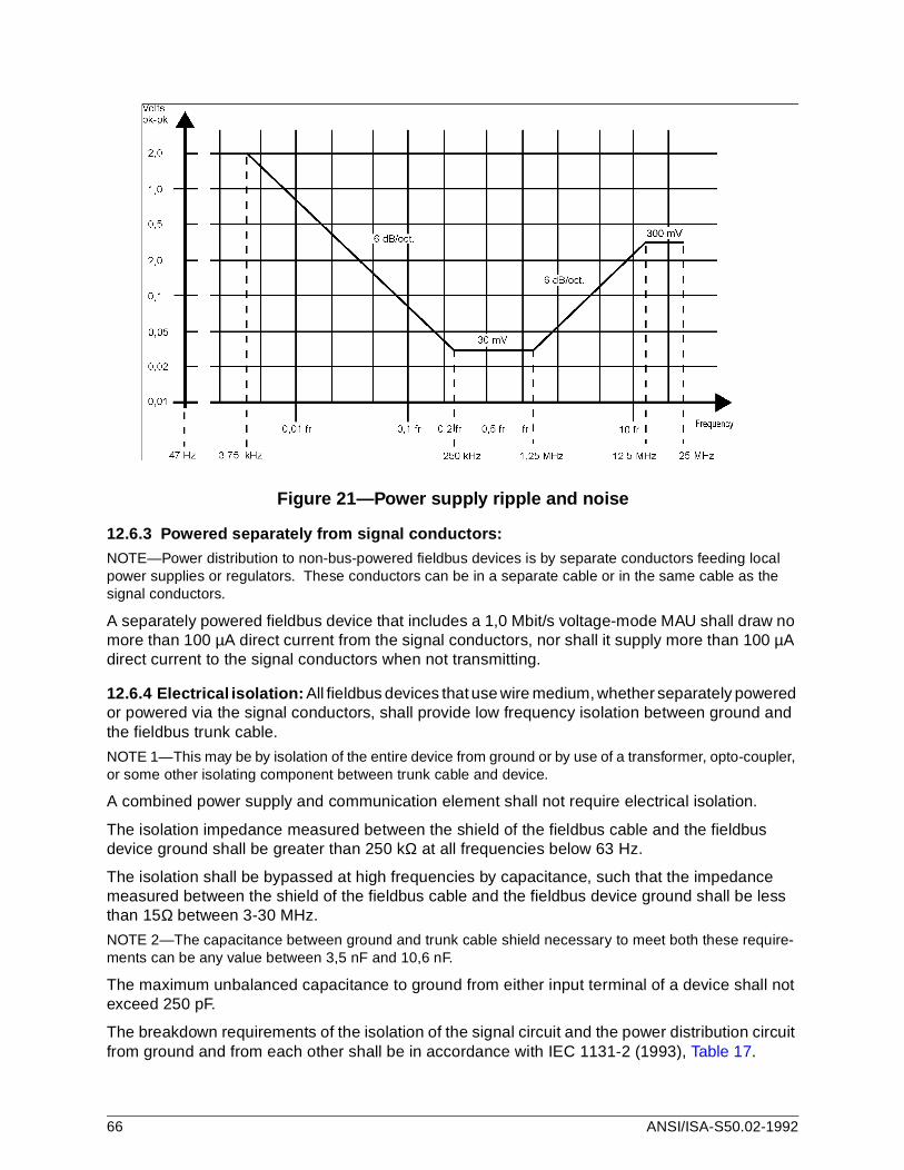
Figure 21—Power supply ripple and noise
12.6.3 Powered separately from signal conductors:
NOTE—Power distribution to non-bus-powered fieldbus devices is by separate conductors feeding local power supplies or regulators. These conductors can be in a separate cable or in the same cable as the signal conductors.
A separately powered fieldbus device that includes a 1,0 Mbit/s voltage-mode MAU shall draw no more than 100 µA direct current from the signal conductors, nor shall it supply more than 100 µA direct current to the signal conductors when not transmitting.
12.6.4 Electrical isolation: All fieldbus devices that use wire medium, whether separately powered or powered via the signal conductors, shall provide low frequency isolation between ground and the fieldbus trunk cable.
NOTE 1—This may be by isolation of the entire device from ground or by use of a transformer, opto-coupler, or some other isolating component between trunk cable and device.
A combined power supply and communication element shall not require electrical isolation.
The isolation impedance measured between the shield of the fieldbus cable and the fieldbus device ground shall be greater than 250 kΩ at all frequencies below 63 Hz.
The isolation shall be bypassed at high frequencies by capacitance, such that the impedance measured between the shield of the fieldbus cable and the fieldbus device ground shall be less than 15Ω between 3-30 MHz.
NOTE 2—The capacitance between ground and trunk cable shield necessary to meet both these require-ments can be any value between 3,5 nF and 10,6 nF.
The maximum unbalanced capacitance to ground from either input terminal of a device shall not exceed 250 pF.
The breakdown requirements of the isolation of the signal circuit and the power distribution circuit from ground and from each other shall be in accordance with IEC 1131-2 (1993), Table 17.
66 ANSI/ISA-S50.02-1992

NOTE 3—For a device that is powered from a supply with rated voltage d 50 V DC or rms, the equivalent test voltages at sea level are 444 V rms, 635 V DC and 635 V peak impulse test. For a device that is powered from a supply with rated voltage between 150 and 300 V rms, the equivalent test voltages at sea level are 2 260 V rms, 3 175 V DC, and 3 175 V peak impulse test.
12.7 Medium specification:
12.7.1 Connector: Cable connectors, if used, shall be to the IEC fieldbus standard (see Annex B). Field termination techniques such as screw or blade terminals and permanent termination may also be used.
12.7.2 Cable: The cable used for testing fieldbus devices with a 1,0 Mbit/s voltage-mode MAU for conformance to the requirements of this part of ISA-S50.02 shall be a single twisted pair cable with overall shield meeting the following minimum requirements at 25°C:
a) Z0 at 0,25 fr (250 kHz) = 150 Ω ± 10%;
b) Z0 at 1,25 fr (1,25 MHz) = 150 Ω ± 10%;
c) maximum attenuation at 0,25 fr (250 kHz) = 6,5 dB/km;
d) maximum attenuation at 1,25 fr (1,25 MHz) = 13 dB/km;
e) maximum capacitive unbalance to shield = 1,5 nF/km
f) maximum DC resistance (per conductor) = 57,1 Ω/km;
g) conductor cross-sectional area (wire size) = nominal 0,33 mm2 (#22 AWG);
h) minimum resistivity between either conductor and shield = 16 GΩ km;
i) minimum shield coverage shall be 95%.
NOTE—Other types of cable may be used, other than for conformance testing. Cables with improved specifications may enable increased trunk length and/or superior interference immunity. Conversely, cables with inferior specifications may be used subject to length limitations for both trunk and spurs plus possible nonconformance to the RFI/EMI susceptibility requirements .
12.7.3 Coupler : The coupler shall provide one or several point(s) of connection to the trunk. It may be integrated in a fieldbus device, in which case there is no spur. Otherwise, it has at least three access points as shown in Figure 22: one for the spur and one for each side of the trunk.
Figure 22—Fieldbus coupler
A passive coupler may contain any or all of the optional elements as described below:
ANSI/ISA-S50.02-1992 67

a) a transformer, to provide galvanic isolation and impedance transformation between trunk and spur;
b) connectors, to provide easy connection to spur and/or trunk;
c) protection resistors, as shown in Figure 23, to protect bus traffic between other stations from the effects of a short circuit spur for separately powered device spurs.
Figure 23—Protection resistors
Active couplers, which require external power supplies, contain components for signal amplification and retransmission. The transmit level and timing requirements shall be according to 12.3.
12.7.4 Splices:
NOTE—A splice is any part of the network in which the characteristic impedance of the network cable is not preserved. This is possibly due to separation of the cable conductors, removal of the cable shield, change of wire gage or type, connection to spurs, attachment to terminal strips, etc. A practical definition of a splice is, therefore, any part of the network that is not a continuous length of the specified medium.
The continuity of all conductors of the cable shall be maintained in a splice.
12.7.5 Terminator : A terminator shall be located at both ends of the trunk cable, connected from one signal conductor to the other. No connection shall be made between terminator and cable shield.
For test purposes, using the cable specified in 12.7.2, the terminator shall have an impedance value of 150 Ω ± 2% over the frequency range 0,25 fr to 1,25 fr (250 kHz to 1,25 MHz).
NOTE—In practical implementations this value would be selected to be approximately equal to the average cable characteristic impedance value at the relevant frequencies to minimize transmission line reflections.
The direct current leakage through the terminator shall not exceed 100 µA. The terminator shall be nonpolarized.
12.7.6 Shielding rules: For full conformance to the noise immunity requirements of 12.4, it is necessary to ensure the integrity of shielding throughout the cabling, connectors, and couplers by the following means:
a) The coverage of the cable shield shall be greater than 95% of the full cable length.
b) Shielding shall completely cover the electrical circuits in connectors, couplers, and splices.
NOTE—Deviation from these shielding rules may degrade noise immunity.
68 ANSI/ISA-S50.02-1992

12.7.7 Grounding rules:
NOTE 1—Grounding means permanently connected to earth through a sufficiently low impedance and with sufficient current carrying capability to prevent voltage buildup, which might result in undue hazard to con-nected equipment or persons. Zero volts (common) lines may be connected to ground where they are galvanically isolated from the fieldbus trunk.
Fieldbus devices shall be required to function to the requirements of this part of ISA-S50.02 with the mid-point of one terminator or one inductive coupler connected directly to ground.
Fieldbus devices shall not connect either conductor of the twisted pair to ground at any point in the network. Signals shall be applied and preserved differentially throughout the network.
NOTE 2—It is standard practice for the shield of the fieldbus trunk cable (if applicable) to be effectively grounded at one point along the length of the cable. For this reason fieldbus devices should allow DC isolation of the cable shield from ground. For bus-powered systems the grounding of the shield and balanced signal conductors would be close to the power supply unit. Capacitive coupling between the shield or the balanced signal conductors and device local ground for EMI control is permitted.
13 Medium Attachment Unit (MAU): current mode, wire medium
NOTES
1 The 1,0 Mbit/s current-mode MAU simultaneously provides access to a communication network and toa power distribution network. Devices attached to the network communicate via the medium and may ormay not be powered from it. Power is distributed as a constant AC current. The communications signalsare superimposed on the AC power.
2 The network medium consists of shielded twisted pair cable.
3 Trapezoidal waveforms are used to reduce electromagnetic emissions and signal distortion.
4 In intrinsically safe applications, available power may limit the number of devices.
5 The devices are connected in series on the bus, whereas in the voltage-mode variants the devices arein parallel.
13.1 Transmitted bit rate: The current-mode transmitted bit rate shall be 1,0 Mbit/s ± 0,01%, averaged over a frame having a minimum length of 16 octets. The instantaneous bit time shall be 1,0 µs 0,025 µs.
13.2 Network specifications:
NOTES
1 A 1,0 Mbit/s current-mode MAU operates in a network composed of the following components:
a) Cable;
b) Terminators;
c) Couplers;
d) Devices (containing at least one communication element).
A wire network in current mode may additionally include the following components:
e) Connectors;
f) Power supplies;
g) Devices that include power supplies;
h) Intrinsic safety barriers.
ANSI/ISA-S50.02-1992 69
2 The network medium consists of shielded twisted pair cable. Independent of topology, all attached devices, other than possibly the transmitting device, are low impedance to prevent significant network load-ing.
13.2.1 Topologies: A wire MAU shall operate in a network with a linear bus topology, consisting of a trunk, terminated at each end in as specified in 13.7.5, to which communication elements are connected via couplers and spurs.
NOTES
1 The coupler and communication element may be integrated in one device (i.e., zero length spur).
2 Tree topology with all the communication elements located at the ends of the trunk is regarded as aspecial case of a bus for the purpose of this part of ISA-S50.02.
3 Several communication elements may be connected to the trunk at one point using a multiport coupler.An active coupler may be used to extend a spur to a length that requires termination to avoid reflections anddistortions. Active repeaters may be used to extend the length of the trunk beyond that of a single segmentas permitted by the network configuration rules.
13.2.2 Network configuration rules: A current-mode MAU shall be required to conform to the requirements of this part of ISA-S50.02 when used in a network that complies with these rules.
Rule 1: One fieldbus shall be capable of communication between 2 and 32 devices, all operating at the same bit rate, both for a powered and a nonpowered bus, and in a hazardous area using distributed barriers.
NOTES
1 The use of a single barrier in the safe area may limit the number of devices in the hazardous area.
2 Rule 1 does not preclude the use of more than the specified number of devices in an installed system.The numbers of devices were calculated on the assumption that a bus-powered device draws 100 mW.
Rule 2: A fully loaded (maximum number of connected devices), current-mode fieldbus segment shall have a total cable length, between any two devices, of up to 750 m.
NOTE 3—750 m maximum cable length is the requirement for conformance to this part of ISA-S50.02, but this does not preclude the use of longer lengths in an installed system.
Rule 3: The total number of waveform regenerations by repeaters and active couplers between any two devices shall not exceed four.
Rule 4: The maximum propagation delay between any two devices shall not exceed 40 nominal bit times.
NOTE 4—For efficiency of the network, that part of the turnaround time of any device on the network caused by a PhE between the end of a received frame and the beginning of the transmitted frame containing an associated immediate response should not exceed 5 bit times, no more than 2 bit times of which should be due to the MAU. As it is not mandatory to expose the DLL-PhL interface or the MDS-MAU interface, that part of the turnaround time of a fieldbus device caused by the PhL or the MAU cannot be specified or conformance tested.
Rule 5: The fieldbus shall be capable of continued operation while a device is being connected or disconnected. Data errors induced during connection or disconnection shall be detected.
Rule 6: Failure of any communication element or spur (including a short circuit or open circuit, but excluding jabber) shall not interfere with transactions between other communication elements for more than 1 ms.
Rule 7: The network shall not be polarity sensitive with or without power injected on the line.
Rule 8: The degradation of the electrical characteristics of the signal between any two devices due to attenuation, attenuation distortion, and mismatching shall be limited to the values indicated below.
70 ANSI/ISA-S50.02-1992

a) Signal attenuation: The signal attenuation due to each device shall not exceed 0,2 dB. The configuration of the bus (trunk and spur lengths, number of devices, I.S. barriers, galvanic isolators, and possible matching devices) shall be such that the attenuation between any two devices at the frequency corresponding to the bit rate shall not exceed 16 dB.
b) Attenuation distortion: The configuration of the bus (trunk and spur lengths and number of devices) shall be such that between any two devices:
[Attenuation (1,25 fr) – Attenuation (0,25 fr)] d 6 dB
Attenuation (1,25 fr) t Attenuation (0,25 fr)
where fr is the frequency corresponding to the bit rate. Attenuation shall be mono-tonic for all frequencies from 0,25 fr to 1,25 fr (250 kHz to 1,25 MHz).
c) Mismatching Distortion: Mismatching (due to spurs or any other effect, including one open circuit spur of maximum length) on the bus shall be such that, at any point along the trunk, in the frequency band 0,25 fr to 1,25 fr (250 kHz to 1,25 MHz):
|(Z – Z0) / (Z + Z0)| d 0,2
where Z0 is the characteristic impedance of the trunk cable and Z is the parallelcombination of Z0 and the load impedance at the coupler.
NOTE 5—Rule 8 minimizes restrictions on trunk and spur length, number of devices, etc., by specifying only the transmission limitations imposed by combinations of these factors. Different combinations may be used depending on the needs of the application.
Rule 9: The following rules shall apply to systems implemented with redundant media:
a) Each channel (cable) shall comply with the network configuration rules.
b) There shall not be a nonredundant segment between two redundant segments.
c) Repeaters shall also be redundant.
d) If the system is configured (by Station Management) to transmit on more than one channel simultaneously, the propagation time difference between any two devices on any two channels shall not exceed five bit times;
e) Channel numbers shall be maintained throughout the fieldbus, i.e., channels 1, 2, 3... from Station Management shall always connect to physical channels 1, 2, 3...
13.2.3 Power distribution rules for network configuration: The cable shield shall not be used as a power conductor.
13.3 Transmit circuit specification for 1,0 Mbit/s current-mode MAU:
NOTE—For ease of reference, the requirements of 13.1 and 13.3 are summarized in Tables 18 and 19.
ANSI/ISA-S50.02-1992 71

Table 18—Transmit level specification summary for current-mode MAU
Table 19—Transmit timing specification summary for current-mode MAU
13.3.1 Test configuration: Figure 24 shows the configuration that shall be used for testing.
Figure 24—Test configuration for current-mode MAU
The test configuration for clause 13 shall be as shown in Figure 24 except where otherwise stated in a specific requirement.
NOTE—Test load resistance R = 320 Ω (twice maximum cable Z0) as the output is loaded by a series loop
of the trunk.
Transmit level characteristics, values referred to trunk(but measured using test load as shown in Figure 24 )
Limits for current mode(bus powered and/or I.S.)
Output level (peak-to-peak, see Figure 25)With Test load ( > 2 x nominal Z0 of trunk cable)
t 2,5 V 320 Ω ± 1%
Maximum positive and negative amplitude difference (signaling bias) as shown in Figure 26
± 0,2 V
Output level; open circuit, (peak-to-peak) d 4,0 V
Maximum output signal distortion; i.e., overvoltage, ringing and droop; (See Figure 25)
± 10%
Quiescent transmitter output; i.e., transmitter noise; (measured over the frequency band 1 kHz to 4 MHz)
d 1 mV (rms)
Transmit timing characteristics, values referred to trunk(but measured using test load as shown in Figure 24 )
Limits for current mode(bus powered and/or I.S.)
Transmitted bit rate 1 Mbit/s ± 0,01%
Instantaneous bit time 1 s 0,025 µs
Rise and fall times (10% to 90% of pk-pk signal, see Figure 25) d 0,2 nominal bit time
Slew rate (at any point from 10% to 90% of pk-pk signal) d 40,0 V / µs
Maximum transmitted bit cell jitter (zero-crossing point deviation, see Figure 26)
± 0,025 nominal bit time
Transmit enable/disable time (i.e., time during which the output waveform may not meet the transmit requirements)
d 2,0 nominal bit times
72 ANSI/ISA-S50.02-1992

13.3.2 Output level requirements:
NOTE—Figure 25 shows an example of one cycle of a fieldbus waveform, illustrating some key items from the transmit circuit specification. Only signal voltages are shown; this diagram takes no account of power supply voltages.
Figure 25—Output waveform
A current-mode MAU transmit circuit shall conform to the following output level requirements, all amplitudes being measured at the estimated midpoint between any peaks or troughs in the top and bottom of the waveform ("midpoint" in Figure 25):
a) The output voltage across the test load after transformer step up/down shall be no less than 2,5 V peak-to-peak with a load resistance of 320 Ω ± 1% ("min o/p" in Figure 25).
b) The output voltage at the trunk, or at the transmit terminals, with any load including an open circuit shall not exceed 4,0 V peak-to-peak ("max o/c at trunk" in Figure 25). For test purposes, open circuit shall be defined as a load of 100 kΩ resistance in parallel with 15 pF capacitance.
c) During transmission a device shall not suffer permanent failure when a load resistance of d 1 Ω is applied for 1 second.
d) The difference between positive amplitude and negative amplitude, measured as shown in Figure 26, shall not exceed ± 0,2 V peak.
e) The output noise from a current-mode MAU that is receiving or not powered shall not exceed 1 mV rms, measured differentially over the frequency band 1 kHz to 4 MHz, referred to the trunk.
f) The differential voltage across the test load shall be such that the voltage monotonically changes between 10% and 90% of peak-to-peak value. Thereafter, the signal voltage shall not vary more than ± 10% of peak-to-peak value until next transition occurs. This permitted variation shall include all forms of output signal distortion, i.e., overvoltage, ringing, and droop.
13.3.3 Output timing requirements: A current-mode MAU transmit circuit shall conform to the following output timing requirements:
ANSI/ISA-S50.02-1992 73

a) Rise and fall times, measured from 10% to 90% of the peak-to-peak signal amplitude, shall not exceed 0,2 nominal bit time (see Figure 25);
b) Slew rate shall not exceed 40 V/µs measured at any point in the range 10% to 90% of the peak-to-peak signal amplitude (see Figure 25).
NOTE—Requirements a) and b) produce a trapezoidal waveform at the transmit circuit output. Requirement b) limits the level of interference emissions that may be coupled to adjacent circuits, etc. Requirement b) is calculated from the formula:
max. slew rate = 3 x min. slew rate = 3 x 0,8 V0 / 0,2 T = 12 x V0 / T
where V0 is an estimated maximum pk-pk output voltage with standard load (3,3V), and T is the nominal bit time (1 µs).
c) Transmitted bit cell jitter shall not exceed ± 0,025 nominal bit time from the ideal zero crossing point, measured with respect to previous zero crossing (see Figure 26).
Figure 26—Transmitted bit cell jitter (zero crossing point deviation)
d) The transmit circuit shall turn on, i.e., the signal shall rise from below the transmit circuit maximum output noise level as specified in 13.3.2 (e) to full output level, in less than 2 nominal bit times. The waveform corresponding to the third and later bit times shall be as specified by other parts of 13.3.
e) The transmit circuit shall turn off, i.e., the signal shall fall from full output level to below the transmit circuit maximum output noise level as specified in 13.3.2 (e), in less than 2 nominal bit times. The time for the transmit circuit to return to its off state impedance shall not exceed 4 nominal bit times. For the purposes of testing, this requirement shall be met with the transmit circuit test configuration of 13.3.1 with the equivalent capacitance of a maximum length cable across the DUT terminals.
NOTE—This requirement is to ensure that the transition of the transmit circuit from active to passive leaves the line capacitance fully discharged.
13.4 Receive circuit specification for 1,0 Mbit/s current-mode MAU
NOTE—For ease of reference, the requirements of 13.4 are summarized in Table 20.
74 ANSI/ISA-S50.02-1992

Table 20—Receive circuit specification summary for current-mode MAU
13.4.1 Input impedance: The differential input impedance of a current-mode MAU receive circuit shall not exceed 2,5 Ω in series with the line over the frequency range 0,25 fr to 1,25 fr (250 kHz to 1,25 MHz). This requirement shall be met in the power-off and power-on (not transmitting) states and in transition between these states. This impedance shall be measured at the inductive coupler using a sinusoidal current waveform with an amplitude greater than the receiver sensitivity threshold and lower than 20 mA peak-to-peak.
NOTE—The requirement for d 2,5 Ω input impedance during power-up and power-down may be met by automatic disabling of the transmitter during these periods.
13.4.2 Receiver sensitivity and noise rejection: A 1,0 Mbit/s current-mode MAU receive circuit shall be capable of accepting an input signal from 1,3 mA peak-to-peak to 20,0 mA peak-to-peak, including overvoltage and oscillation (see "signal level" in Figure 27 together with "positive ampli-tude" and "negative amplitude" in Figure 25).
A 1,0 Mbit/s current-mode MAU receive circuit shall not respond to an input signal with a peak-to-peak line current amplitude that does not exceed 0,8 mA (see "noise rejection" in Figure 27).
Figure 27—Receiver sensitivity and noise rejection
13.4.3 Interference susceptibility and error rates:NOTE 1—When the fieldbus is operating in a variety of standard noise environments, the probability that an Application Layer User Data Unit contains an undetected error, due to operation of the conveying Physical
and Data Link Layer entities, should be less than 1 in 1012 (1 error in 20 years at 1 600 messages/s). A communication element is regarded as conforming to this theoretical requirement when it meets the following interference susceptibility requirements. These are specified by a detected frame error rate, which is derived
by using a ratio of detected to undetected errors of 106. This follows the IEEE 802 Functional Requirements Document, Draft 5.9, sections 5.6.1 and 5.6.2, and should be readily achievable with a 16-bit Frame Check Sequence at the Data Link Layer.
A communication element that includes a current-mode MAU, operating with frames containing 64 random user data bits, with maximum frame rate, and with signals of 4,0 mA pk-pk amplitude
Receive circuit characteristics(values referred to trunk)
Limits for current mode(bus powered and/or I.S.)
Input impedance, measured over the frequency range 0,25 fr to 1,25 fr d 2,5 Ω
Sensitivity; min. pk-pk signal required to be accepted (see Figure 27) 1,3 mA
Noise rejection; max. pk-pk noise required to be rejected (see Figure 27) 0,8 mA
Maximum received bit cell jitter (zero-crossing point deviation, see Figure 29) ± 0,10 nominal bit time
ANSI/ISA-S50.02-1992 75

shall produce no more than 3 detected frame errors in 3 x 10⁶ frames during operation in the presence of common mode voltage or Gaussian noise as follows:
a) a common mode sinusoidal signal of any frequency from 63 Hz to 2 MHz, with an amplitude of 4 V r.m.s. and from 47 Hz to 63 Hz with an amplitude of 250 V rms;
b) a common mode DC signal of ± 10 V;
c) white Gaussian additive differential noise in the frequency band 1 kHz to 4 MHz, with a noise density of 0,09 A/ using the test circuit of Figure 28.
NOTE 2—The common mode voltage and Gaussian noise specifications are for receive circuit conformance testing with balanced loads and are not indicative of system installation practice.
A communication element that includes a current-mode MAU, operating with frames containing 64 random user data bits, at an average of 1 600 messages per second, with signals of 4,0 mA pk-pk amplitude shall produce no more than 6 detected frame errors in 100 000 frames during operation in the presence of electromagnetic or electrical interference environments as follows:
a) 10 V/m electromagnetic field as specified in IEC 801-3 at severity level 3;
b) electrical fast transient as specified in IEC 801-4 at severity level 3.
The above error rate specification shall also be satisfied after but not during operation in the following noise environments:
a) 8 kV electrostatic discharge to exposed metalwork as specified in IEC 801-2 at severity level 3. If the device suffers temporary loss of function or performance as a result of this test it shall recover from any such loss without operator intervention within 3 seconds after the end of the test.
b) High frequency disturbance tests as specified in IEC 255-4 Appendix E, test voltage class III (2,5 kV and 1 kV peak values of first half-cycle in longitudinal and transverse mode, respectively). If the device suffers temporary loss of function or performance as a result of this test, it shall recover from any such loss without operator intervention within 3 seconds after the end of the test.
Figure 28—Noise test circuit for current-mode MAU
13.4.4 Received bit cell jitter: The receive circuit shall accept a Manchester encoded signal transmitted in accordance with 13.1 and 13.3. In addition, the receiver shall work properly with
Hz rms
76 ANSI/ISA-S50.02-1992

signals with the time variation between any two adjacent signal transition points (zero crossing) of ±0,10 nominal bit time or less. See Figure 29.
NOTES
1 This does not preclude the use of receivers that perform better than this specification.
2 Depending on the symbol pattern, the nominal time between zero crossings may be one half or one bittime.
3 There is no requirement to reject a signal with a specified time variation value. The receiver reports anerror when the received bit cell jitter exceeds the receiver's ability to reliably decode signaling.
Figure 29—Received bit cell jitter
13.5 Jabber inhibit: The MAU shall contain a self-interrupt capability to inhibit transmitted signals from reaching the medium. Hardware within the MAU (with no external message other than the detection of output signals or leakage via the transmit function) shall provide a window of between 5 ms and 15 ms, during which time a normal frame may be transmitted. If the frame length exceeds this duration, the jabber inhibit function shall inhibit further output signals from reaching the medium and shall disable echo on the RxS line (see 10.2.2) to indicate jabber detection to the MDS.
The MAU shall reset the self-interrupt function after a period of 500 ms ± 50%.
NOTE—This inhibits bus traffic for no more than 3% (| 1/32) of the available time.
13.6 Power distribution:
NOTES
1 A device can optionally receive power via the signal conductors or be separately powered.
2 A device can be certified as intrinsically safe with either method of receiving power.
3 This part of ISA-S50.02 does not include requirements for I.S. certification but seeks to exclude condi-tions or situations that would prevent I.S. certification.
4 A separately powered device can be connected to a powered fieldbus.
5 For ease of reference, the requirements of 13.6 are summarized in Table 21.
ANSI/ISA-S50.02-1992 77

Table 21—Network power supply requirements for the current-mode MAU
13.6.1 Powered via signal conductors: A device shall operate over a range of constant currents from 50 mA to 200 mA.
NOTE—The output voltage from the supply is a function of cable loss and power consumed per device. A fieldbus device may be designed to consume one or more standard loads. A standard load is 100 mW.
The power supply open-circuit output voltage shall be less than the limit specified by the local regulatory agency for the particular implementation. The output impedance of the power supply shall be d 5 Ω over the frequency range 0,25 fr to 1,25 fr (250 kHz to 1,25 MHz).
The voltage drop in the signal coupler shall be less than 0,1 V at 16 kHz.
The voltage drop in the terminations shall be less than 0,3 V at 16 kHz.
The power waveform shall be a clean sinusoid of frequency 16 kHz ± 0,5% and maximum harmonic distortion of 0,2%.
The device shall not introduce harmonic components of the power frequency larger than 1,0 mV peak-to-peak line-to-line in the main trunk.
13.6.2 Powered separately from signal
NOTE—Power distribution to non-bus-powered fieldbus devices is by separate conductors feeding local power supplies, regulators, or safety barriers. I.S. certification may require these conductors to be in a separate cable from the signal conductors and may also impose more stringent requirements for current levels than specified.
A separately powered fieldbus device that includes a 1,0 Mbit/s current-mode MAU shall drop no more than 1 mV rms at the power frequency on the signal conductors, nor shall it supply a current of more than 100 A rms to the signal conductors when not transmitting.
13.6.3 Electrical isolation: All fieldbus devices that use wire medium, whether separately powered or powered via the signal conductors, shall provide low frequency isolation between ground and the fieldbus trunk cable.
NOTE 1—This may be by use of an inductive coupler with sufficient isolation specification, by isolation of the entire device from ground or by use of a transformer, opto-coupler, or some other isolating component between trunk cable and device.
A combined power supply and communication element shall not require electrical isolation.
The isolation impedance measured between the shield of the fieldbus cable and the fieldbus device ground shall be greater than 250 kΩ at all frequencies below 63 Hz.
The isolation shall be bypassed at high frequencies by capacitance, such that the impedance measured between the shield of the fieldbus cable and the fieldbus device ground shall be less than 15 Ω between 3-30 MHz.
NOTE 2—The capacitance between ground and trunk cable shield necessary to meet both these require-ments can be any value between 3,5 nF and 10,6 nF.
Network power supply requirements Limits for 1,0 Mbit/s current mode
Output current 50 to 200 mA rms
Output frequency 16 kHz ± 0,5%
Maximum output voltage, I.S. Depends on barrier rating
Harmonic distortion of supply current d 0,2%
Output impedance, measured over the frequency range 0,25 fr to 1,25 fr d 5 Ω
78 ANSI/ISA-S50.02-1992

The maximum unbalanced capacitance to ground from either input terminal of a device shall not exceed 250 pF.
The breakdown requirements of the isolation of the signal circuit and the power distribution circuit from ground and from each other shall be in accordance with IEC 1131-2 (1993), Table 17.
NOTE 3—For a device that is powered from a supply with rated voltage d 50 V DC or rms, the equivalent test voltages at sea level are 444 V rms, 635 V DC and 635 V peak impulse test. For a device that is powered from a supply with rated voltage between 150 and 300 V rms, the equivalent test voltages at sea level are 2 260 V rms, 3 175 V DC and 3 175 V peak impulse test.
13.7 Medium specification:
13.7.1 Connector: Cable connectors, if used, shall be to the IEC fieldbus standard (see Annex B). Field termination techniques such as screw or blade terminals and permanent termination may also be used.
13.7.2 Cable: The cable used for testing fieldbus devices with a current-mode MAU for conform-ance to the requirements of this part of ISA-S50.02 shall be a single twisted pair cable with overall shield meeting the following minimum requirements at 25°C:
a) Z0 at 0,25 fr (250 kHz) = 150 Ω ±10%;
b) Z0 at 1,25 fr (1,25 MHz) = 150 Ω ± 10%;
c) maximum attenuation at 0,25 fr (250 kHz) = 6,5 dB/km;
d) maximum attenuation at 1,25 fr (1,25 MHz) = 13 dB/km;
e) maximum capacitive unbalance to shield = 1,5 nF/kmf) maximum DC resistance (per conductor) = 57,1 Ω/km;
g) conductor cross-sectional area (wire size) = nominal 0,33 mm2 (#22 AWG);h) minimum resistivity between either conductor and shield = 16 GΩ km;i) minimum shield coverage shall be 95%.
NOTES
1 Other types of cable may be used, other than for conformance testing. Cables with improved specifi-cations may enable increased trunk length and/or superior interference immunity. Conversely, cables withinferior specifications may be used subject to length limitations for both trunk and spurs plus possible non-conformance to the RFI/EMI susceptibility requirements.
2 For intrinsically safe applications the inductance/resistance ratio (L/R) should be less than the limitspecified by the local regulatory agency for the particular implementation.
13.7.3 Coupler: An inductive coupler connects one device or spur to the trunk. It transfers data signals to and from the device and may transfer power to the device. The trunk cable operates as a single primary turn in the inductive coupler transformer. The following options are permitted:
a) The coupling may be performed without violation of the cable insulation.
b) The inductive coupler may be used as a connector.
c) An I.S. barrier element may be included as an integral part of the inductive coupler.
The coupler shall be an integral part of the MAU if the device is connected in the trunk. The input impedance of the coupler shall be a maximum of 2,5 Ω in series with the line.
13.7.4 Splices:
NOTE—A splice is any part of the network in which the characteristic impedance of the network cable is not preserved. This is possibly due to separation of the cable conductors, removal of the cable shield, change of wire gage or type, connection to spurs, etc. A practical definition of a splice is, therefore, any part of the
ANSI/ISA-S50.02-1992 79

network that is not a continuous length of the specified medium.
The continuity of all conductors of the cable shall be maintained in a splice.
13.7.5 Terminator: A terminator shall be located at both ends of the trunk cable, connected from one signal conductor to the other. No connection shall be made between terminator and cable shield.
For test purposes, using the cable specified in 13.7.2, the terminator shall have an impedance value of 120 Ω ± 2% over the frequency range 0,25 fr to 1,25 fr (250 kHz to 1,25 MHz).
NOTES
1 The terminator resistance value was selected to be lower than the test cable characteristic impedancevalue because the current-mode devices add impedances in series with the terminator. The value was cho-sen to reduce transmission line reflections for a fieldbus with 2 to 32 devices.
2 In practical implementations with power supplied via the signal conductors the terminator would be by-passed at power frequencies to minimize power losses.
The direct current leakage through the terminator shall not exceed 100 µA. The terminator shall be nonpolarized.
All terminators used for I.S. applications shall comply with isolation requirements (creepage and clearance) commensurate with the required I.S. approval. Terminators for non-I.S. applications shall not be required to have I.S. approval.
13.7.6 Shielding rules: For full conformance to the noise immunity requirements of 13.4, it is necessary to ensure the integrity of shielding throughout the cabling, connectors, and couplers by the following means:
a) The coverage of the cable shield shall be greater than 95% of the full cable length.
b) Shielding shall completely cover the electrical circuits in connectors, couplers, and splices.
NOTE—Deviation from these shielding rules may degrade noise immunity.
13.7.7 Grounding rules:
NOTE 1—Grounding means permanently connected to earth through a sufficiently low impedance and with sufficient current carrying capability to prevent voltage buildup, which might result in undue hazard to connected equipment or persons. Zero volts (common) lines may be connected to ground where they are galvanically isolated from the fieldbus trunk.
Fieldbus devices shall not connect either conductor of the twisted pair to ground at any point in the network. Signals shall be applied and preserved differentially throughout the network.
NOTE 2—It is standard practice for the shield of the fieldbus trunk cable (if applicable) to be effectively grounded at one point along the length of the cable. For this reason fieldbus devices should allow DC isolation of the cable shield from ground. For bus-powered systems, the grounding of the shield and balanced signal conductors would be close to the power supply unit. For I.S. systems, the grounding would be at the safety barrier earth connection. Capacitive coupling between the shield or the balanced signal conductors and device local ground for EMI control is permitted subject to I.S. requirements.
80 ANSI/ISA-S50.02-1992
14 Medium Attachment Unit (MAU): 2,5 Mbit/s, voltage mode, wire medium
NOTES
1 The 2,5 Mbit/s voltage-mode MAU requirements are not specifically intended to facilitate the optionsof power distribution via the signal conductors and suitability for intrinsic safety certification. If bus powered,power is distributed as direct voltage and current, and communications signals are superimposed on the DCpower.
2 The network medium consists of shielded twisted pair cable. Independent of topology, all attacheddevices, other than possibly the transmitting device, are high impedance to prevent significant networkloading. Trapezoidal waveforms are used to reduce electromagnetic emissions and signal distortion.
3 A linear bus topology is supported. A network contains one trunk cable, terminated at both ends.
14.1 Transmitted bit rate: The transmitted bit rate shall be 2,5 Mbit/s ± 0,01%, averaged over a frame having a minimum length of 16 octets. The instantaneous bit time shall be 0,4 µs ± 0,010 µs.
14.2 Network specifications:
NOTE—A 2,5 Mbit/s voltage-mode MAU operates in a network composed of the following components:
a) Cable;
b) Terminators;
c) Couplers;
d) Devices (containing at least one communication element).
A wire network in 2,5 Mbit/s voltage mode may additionally include the following compo-nents:
e) Connectors;
f) Power supplies;
g) Devices that include power supplies.
14.2.1 Topologies: A wire MAU shall operate in a network with a linear bus topology, consisting of a trunk, terminated at each end as specified in 14.7.5, to which communication elements are connected via couplers. Each communication element shall be connected in parallel with the trunk cable.
NOTES
1 The coupler and communication element are generally integrated in one device.
2 Active repeaters may be used to establish branches or to extend the length of the trunk beyond that ofa single segment as permitted by the network configuration rules. Branches must be considered as seg-ments.
14.2.2 Network configuration rules: A 2,5 Mbit/s voltage-mode MAU shall be required to conform to the requirements of this part of ISA-S50.02 when used in a network that complies with these rules.
Rule 1: One fieldbus shall be capable of communication between 2 and 32 devices, all operating at the same bit rate.
NOTE 1—Rule 1 does not preclude the use of more than the specified number of devices in an installed system.
ANSI/ISA-S50.02-1992 81

Rule 2: A fully loaded (maximum number of connected devices) 2,5 Mbit/s voltage-mode fieldbus segment shall have a total cable length, including branches, between any two devices, of up to 500 m.
NOTE 2—500 m maximum cable length is the requirement for conformance to this part of ISA-S50.02, but this does not preclude the use of longer lengths in an installed system.
Rule 3: The total number of waveform regenerations by repeaters and active couplers between any two devices shall not exceed four.
Rule 4: The maximum propagation delay between any two devices shall not exceed 40 nominal bit times.
NOTE 3—For efficiency of the network, that part of the turnaround time of any device on the network caused by a PhE between the end of a received frame and the beginning of the transmitted frame containing an associated immediate response should not exceed 5 bit times, no more than 2 bit times of which should be due to the MAU. As it is not mandatory to expose the DLL-PhL interface or the MDS-MAU interface, that part of the turnaround time of a fieldbus device caused by the PhL or the MAU cannot be specified or conformance tested.
Rule 5: The fieldbus shall be capable of continued operation while a device is being connected or disconnected. Data errors induced during connection or disconnection shall be detected.
Rule 6: For a 2,5 Mbit/s wire fieldbus that is not powered via the signal conductors, a single failure in any one communication element (including a short circuit but excluding jabber) shall not interfere with transactions between other communication elements for more than 1 ms.
Rule 7: In polarity sensitive systems the medium twisted pairs shall have distinctly marked conductors that uniquely identify individual conductors. The polarization shall be maintained at all connection points.
Rule 8: The degradation of the electrical characteristics of the signal, between any two devices, due to attenuation, attenuation distortion, and mismatching shall be limited to the values indicated below.
a) Signal attenuation: The configuration of the bus (trunk length, number of devices, and possible matching devices) shall be such that the attenuation between any two devices at the frequency corresponding to the bit rate shall not exceed 18 dB.
b) Attenuation distortion: The configuration of the bus (trunk length and number of devices) shall be such that between any two devices:
[Attenuation (1,25 fr) – Attenuation (0,25 fr)] d 10 dB
Attenuation (1,25 fr) t Attenuation (0,25 fr)
where fr is the frequency corresponding to the bit rate. Attenuation shall be mono-tonic for all frequencies from 0,25 fr to 1,25 fr (625 kHz to 3,125 MHz).
c) Mismatching Distortion: Mismatching (due to any effect) on the bus shall be such that, at any point along the trunk, in the frequency band 0,25 fr to 1,25 fr (625 kHz to 3,125 MHz):
|(Z – Z0) / (Z + Z0)| d 0,2
where Z0 is the characteristic impedance of the trunk cable, and Z is the parallelcombination of Z0 and the load impedance at the coupler.
NOTE 4—Rule 8 minimizes restrictions on trunk length, number of devices, etc., by specifying only the transmission limitations imposed by combinations of these factors. Different combinations may be used depending on the needs of the application.
82 ANSI/ISA-S50.02-1992

NOTE 5—The main cause of a large mismatch is the concentration of several couplers on a short length of the trunk.
If the distance between two consecutive couplers is less than 2 m, the propagation delay between them is smaller than 10 ns (1/8 of the maximum rise or fall times specified for the transmit signal), and the concen-tration appears as a single mismatched element inducing large reflections of the signal transitions.
A concentration of couplers where the distance between two consecutive couplers is less than 2 m is defined as a cluster.
In order to comply with the Rule 8 c) using devices with an input impedance of minimum value (8 kΩ) and zero length spurs, it is recommended that a cluster would not include more than four couplers.
Using devices with an input impedance significantly higher than the minimum value would allow clusters with more couplers. Using non-zero length spurs could require clusters to have fewer than four couplers.
NOTE 6—It is possible to reduce the mismatching due to a cluster by the following means:
— using active multiport couplers;
— inserting matching devices (passive attenuators) each side of the cluster, under the condition that the Rule 8 b) is satisfied.
Rule 9: The following rules shall apply to systems implemented with redundant media:
a) Each channel (cable) shall comply with the network configuration rules.
b) There shall not be a nonredundant segment between two redundant segments.
c) Repeaters shall also be redundant.
d) If the system is configured (by Station Management) to transmit on more than one channel simultaneously, the propagation time difference between any two devices on any two channels shall not exceed five bit times.
e) Channel numbers shall be maintained throughout the fieldbus, i.e., channels 1, 2, 3... from Station Management shall always connect to physical channels 1, 2, 3...
14.2.3 Power distribution rules for network configuration: The cable shield shall not be used as a power conductor.
14.3 Transmit circuit specification for 2,5 Mbit/s voltage-mode MAU:
NOTE—For ease of reference, the requirements of 14.1 and 14.3 are summarized in Tables 22 and 23.
Table 22—Transmit level specification summary for 2,5 Mbit/s voltage-mode MAU
Transmit level characteristics, values referred to trunk(but measured using test load as shown in Figure 30 )
Limits for 2,5 Mbit/s voltage mode
Output level (peak-to-peak, see Figure 31); With test load (non-standard for this test)
5,5 V to 9,0 V50 Ω ± 1%
Maximum positive and negative amplitude difference (signaling bias) as shown in Figure 32
± 0,35 V
Output level; open circuit, (peak-to-peak) d 30,0 V
Maximum output signal distortion; i.e., overvoltage, ringing, and droop (See Figure 31)
± 10%
Quiescent transmitter output; i.e., transmitter noise(measured over the frequency band 1 kHz to 10 MHz)
d 10 mV (rms)
ANSI/ISA-S50.02-1992 83

Table 23—Transmit timing specification summary for 2,5 Mbit/s voltage-mode MAU
14.3.1 Test configuration: Figure 30 shows the configuration that shall be used for testing.
Figure 30—Transmit circuit test configuration
Differential signal voltage: Vd = Va – Vb
Test load resistance R = 75 Ω (0,5 cable Z0) and C = 0,15 µF except where otherwise stated in a specific requirement.
14.3.2 Output level requirements:
NOTE—Figure 31 shows an example of the AC component of one cycle of a fieldbus waveform, illustrating some key items from the transmit circuit specification. Only signal voltages are shown; this diagram takes no account of power supply voltages.
Transmit timing characteristics, values referred to trunk(but measured using test load as shown in Figure 30 )
Limits for 2,5 Mbit/s voltage mode
Transmitted bit rate 2,5 Mbit/s ± 0,01%
Instantaneous bit time 0,4 µs ± 0,010 µs
Rise and fall times (10% to 90% of pk-pk signal, see Figure 31) d 0,2 nominal bit time
Slew rate (at any point from 10% to 90% of pk-pk signal) d 250 V / µs
Maximum transmitted bit cell jitter(zero-crossing point deviation, see Figure 32)
± 0,025 nominal bit time
Transmit enable/disable time (i.e., time during which the output waveform may not meet the transmit requirements)
d 2,0 nominal bit times
84 ANSI/ISA-S50.02-1992

Figure 31—Output waveform
A 2,5 Mbit/s voltage-mode MAU transmit circuit shall conform to the following output level requirements, all amplitudes being measured at the estimated midpoint between any peaks or troughs in the top and bottom of the waveform ("midpoint" in Figure 31):
a) The output voltage across the test load after transformer step up/down (if applicable) shall be between 5,5 V and 9,0 V peak-to-peak for all load resistances from 50 Ω ±1% to 75 Ω ± 1% ("min o/p" in Figure 31).
b) The output voltage at the trunk, or at the transmit terminals, with any load including an open circuit shall not exceed 30,0 V peak-to-peak ("max o/c at trunk" in Figure 31). For test purposes, open circuit shall be defined as a load of 100 kΩ resistance in parallel with 15 pF capacitance.
c) During transmission a device shall not suffer permanent failure when a load resistance of t 1 Ω is applied for 1 second.
d) The difference between positive amplitude and negative amplitude, measured as shown in Figure 32, shall not exceed ± 0,35 V peak.
e) The output noise from a 2,5 Mbit/s voltage-mode MAU that is receiving or not powered shall not exceed 10 mV rms, measured differentially over the frequency band 1 kHz to 10 MHz, referred to the trunk.
f) The differential voltage across the test load shall be such that the voltage monotonically changes between 10% and 90% of peak-to-peak value. Thereafter, the signal voltage shall not vary more than ± 10% of peak-to-peak value until next transition occurs. This permitted variation shall include all forms of output signal distortion, i.e., overvoltage, ringing, and droop.
14.3.3 Output timing requirements: A 2,5 Mbit/s voltage-mode MAU transmit circuit shall conform to the following output timing requirements:
ANSI/ISA-S50.02-1992 85
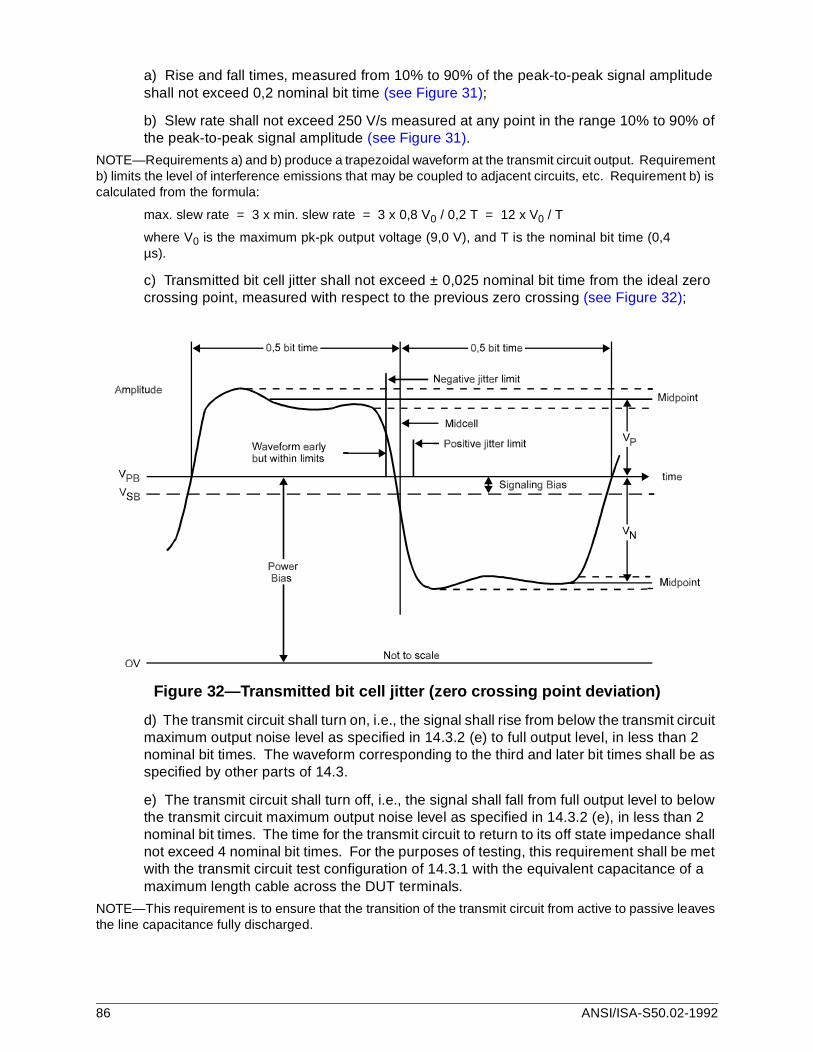
a) Rise and fall times, measured from 10% to 90% of the peak-to-peak signal amplitude shall not exceed 0,2 nominal bit time (see Figure 31);
b) Slew rate shall not exceed 250 V/s measured at any point in the range 10% to 90% of the peak-to-peak signal amplitude (see Figure 31).
NOTE—Requirements a) and b) produce a trapezoidal waveform at the transmit circuit output. Requirement b) limits the level of interference emissions that may be coupled to adjacent circuits, etc. Requirement b) is calculated from the formula:
max. slew rate = 3 x min. slew rate = 3 x 0,8 V0 / 0,2 T = 12 x V0 / T
where V0 is the maximum pk-pk output voltage (9,0 V), and T is the nominal bit time (0,4µs).
c) Transmitted bit cell jitter shall not exceed ± 0,025 nominal bit time from the ideal zero crossing point, measured with respect to the previous zero crossing (see Figure 32);
Figure 32—Transmitted bit cell jitter (zero crossing point deviation)
d) The transmit circuit shall turn on, i.e., the signal shall rise from below the transmit circuit maximum output noise level as specified in 14.3.2 (e) to full output level, in less than 2 nominal bit times. The waveform corresponding to the third and later bit times shall be as specified by other parts of 14.3.
e) The transmit circuit shall turn off, i.e., the signal shall fall from full output level to below the transmit circuit maximum output noise level as specified in 14.3.2 (e), in less than 2 nominal bit times. The time for the transmit circuit to return to its off state impedance shall not exceed 4 nominal bit times. For the purposes of testing, this requirement shall be met with the transmit circuit test configuration of 14.3.1 with the equivalent capacitance of a maximum length cable across the DUT terminals.
NOTE—This requirement is to ensure that the transition of the transmit circuit from active to passive leaves the line capacitance fully discharged.
86 ANSI/ISA-S50.02-1992
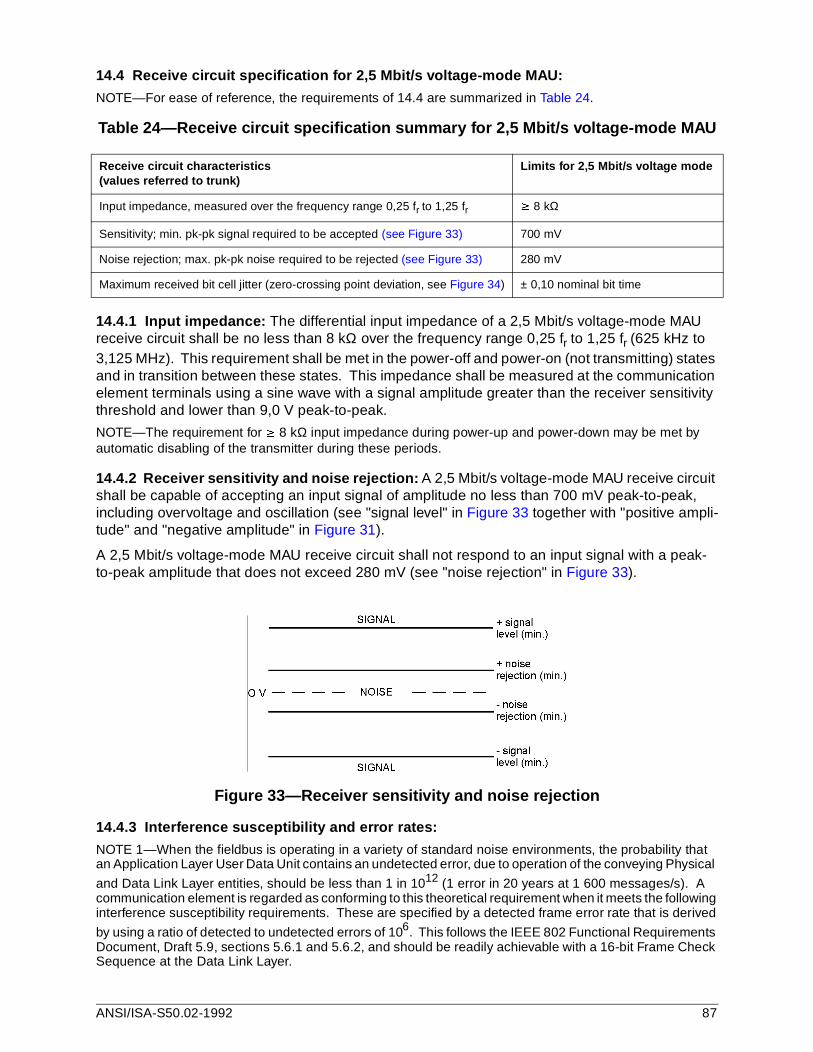
14.4 Receive circuit specification for 2,5 Mbit/s voltage-mode MAU:
NOTE—For ease of reference, the requirements of 14.4 are summarized in Table 24.
Table 24—Receive circuit specification summary for 2,5 Mbit/s voltage-mode MAU
14.4.1 Input impedance: The differential input impedance of a 2,5 Mbit/s voltage-mode MAU receive circuit shall be no less than 8 kΩ over the frequency range 0,25 fr to 1,25 fr (625 kHz to 3,125 MHz). This requirement shall be met in the power-off and power-on (not transmitting) states and in transition between these states. This impedance shall be measured at the communication element terminals using a sine wave with a signal amplitude greater than the receiver sensitivity threshold and lower than 9,0 V peak-to-peak.
NOTE—The requirement for t 8 kΩ input impedance during power-up and power-down may be met by automatic disabling of the transmitter during these periods.
14.4.2 Receiver sensitivity and noise rejection: A 2,5 Mbit/s voltage-mode MAU receive circuit shall be capable of accepting an input signal of amplitude no less than 700 mV peak-to-peak, including overvoltage and oscillation (see "signal level" in Figure 33 together with "positive ampli-tude" and "negative amplitude" in Figure 31).
A 2,5 Mbit/s voltage-mode MAU receive circuit shall not respond to an input signal with a peak-to-peak amplitude that does not exceed 280 mV (see "noise rejection" in Figure 33).
Figure 33—Receiver sensitivity and noise rejection
14.4.3 Interference susceptibility and error rates:
NOTE 1—When the fieldbus is operating in a variety of standard noise environments, the probability that an Application Layer User Data Unit contains an undetected error, due to operation of the conveying Physical
and Data Link Layer entities, should be less than 1 in 1012 (1 error in 20 years at 1 600 messages/s). A communication element is regarded as conforming to this theoretical requirement when it meets the following interference susceptibility requirements. These are specified by a detected frame error rate that is derived
by using a ratio of detected to undetected errors of 106. This follows the IEEE 802 Functional Requirements Document, Draft 5.9, sections 5.6.1 and 5.6.2, and should be readily achievable with a 16-bit Frame Check Sequence at the Data Link Layer.
Receive circuit characteristics(values referred to trunk)
Limits for 2,5 Mbit/s voltage mode
Input impedance, measured over the frequency range 0,25 fr to 1,25 fr t 8 kΩ
Sensitivity; min. pk-pk signal required to be accepted (see Figure 33) 700 mV
Noise rejection; max. pk-pk noise required to be rejected (see Figure 33) 280 mV
Maximum received bit cell jitter (zero-crossing point deviation, see Figure 34) ± 0,10 nominal bit time
ANSI/ISA-S50.02-1992 87

A communication element that includes a 2,5 Mbit/s voltage-mode MAU, operating with frames containing 64 random user data bits, with maximum frame rate and with signals of 1,4 V pk-pk
amplitude shall produce no more than 3 detected frame errors in 3 x 10⁶ frames during operation in the presence of common mode voltage or Gaussian noise as follows:
a) a common mode sinusoidal signal of any frequency from 63 Hz to 5 MHz, with an amplitude of 4 V rms and from 47 Hz to 63 Hz with an amplitude of 250 V rms;
b) a common mode DC signal of ± 10 V;
c) white Gaussian additive differential noise in the frequency band 1 kHz to 10 MHz, with a noise density of 20 V/
NOTE 2—The common mode voltage and Gaussian noise specifications are for receive circuit conformance testing with balanced loads and are not indicative of system installation practice.
A communication element that includes a 2,5 Mbit/s voltage-mode MAU, operating with frames containing 64 random user data bits, at an average of 1 600 messages per second, and with signals of 1,4 V pk-pk amplitude shall produce no more than 6 detected frame errors in 100 000 frames during operation in the presence of electromagnetic or electrical interference environments as follows:
a) 10 V/m electromagnetic field as specified in IEC 801-3 at severity level 3;
b) Electrical fast transient as specified in IEC 801-4 at severity level 3.
The above error rate specification shall also be satisfied after but not during operation in the following noise environments:
a) 8 kV electrostatic discharge to exposed metalwork as specified in IEC 801-2 at severity level 3. If the device suffers temporary loss of function or performance as a result of this test, it shall recover from any such loss without operator intervention within 3 seconds after the end of the test.
b) High frequency disturbance tests as specified in IEC 255-4 Appendix E, test voltage class III (2,5 kV and 1 kV peak values of first half-cycle in longitudinal and transverse mode, respectively). If the device suffers temporary loss of function or performance as a result of this test, it shall recover from any such loss without operator intervention within 3 seconds after the end of the test.
14.4.4 Received bit cell jitter: The receive circuit shall accept a Manchester encoded signal transmitted in accordance with 14.1 and 14.3. In addition, the receiver shall work properly with signals with the time variation between any two adjacent signal transition points (zero crossing) of ± 0,10 nominal bit time or less. (See Figure 34).
NOTES
1 This does not preclude the use of receivers that perform better than this specification.
2 Depending on the symbol pattern, the nominal time between zero crossings may be one half or one bittime.
3 There is no requirement to reject a signal with a specified time variation value. The receiver reports anerror when the received bit cell jitter exceeds the receiver's ability to reliably decode signaling.
Hz rms
88 ANSI/ISA-S50.02-1992
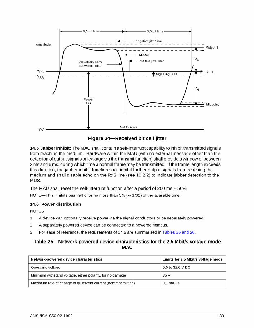
Figure 34—Received bit cell jitter
14.5 Jabber inhibit: The MAU shall contain a self-interrupt capability to inhibit transmitted signals from reaching the medium. Hardware within the MAU (with no external message other than the detection of output signals or leakage via the transmit function) shall provide a window of between 2 ms and 6 ms, during which time a normal frame may be transmitted. If the frame length exceeds this duration, the jabber inhibit function shall inhibit further output signals from reaching the medium and shall disable echo on the RxS line (see 10.2.2) to indicate jabber detection to the MDS.
The MAU shall reset the self-interrupt function after a period of 200 ms ± 50%.
NOTE—This inhibits bus traffic for no more than 3% (| 1/32) of the available time.
14.6 Power distribution:
NOTES
1 A device can optionally receive power via the signal conductors or be separately powered.
2 A separately powered device can be connected to a powered fieldbus.
3 For ease of reference, the requirements of 14.6 are summarized in Tables 25 and 26.
Table 25—Network-powered device characteristics for the 2,5 Mbit/s voltage-mode MAU
Network-powered device characteristics Limits for 2,5 Mbit/s voltage mode
Operating voltage 9,0 to 32,0 V DC
Minimum withstand voltage, either polarity, for no damage 35 V
Maximum rate of change of quiescent current (nontransmitting) 0,1 mA/µs
ANSI/ISA-S50.02-1992 89

Table 26—Network power supply requirements for the 2,5 Mbit/s voltage-mode MAU
14.6.1 Supply voltage: A fieldbus device that includes a 2,5 Mbit/s voltage-mode MAU shall be capable of operating within a voltage range of 9 V to 32 V DC between the two conductors including ripple. The device shall withstand a minimum voltage of ±35 V DC without damage.
A fieldbus device that includes a 2,5 Mbit/s voltage-mode MAU shall conform to the requirements of this part of ISA-S50.02 when powered by a supply with the following specifications:
a) The output voltage of the power supply shall be 32 V DC maximum including ripple.
NOTE 1—The voltage of the power supply added to the open circuit transmitter output voltage should be less than the limit specified by the local regulatory agency for the particular implementation.
b) The output impedance of the power supply shall be t 8 kΩ over the frequency range 0,25 fr to 1,25 fr (625 kHz to 3,125 MHz).
c) The breakdown requirements of the isolation of the signal circuit and the power distribution circuit from ground and from each other shall be in accordance with IEC 1131-2 (1993), Table 17.
NOTE 2—For a device that is powered from a supply with rated voltage d 50 V DC or rms, the equivalent test voltages at sea level are 444 V rms, 635 V DC and 635 V peak impulse test. For a device that is powered from a supply with rated voltage between 150 and 300 V rms, the equivalent test voltages at sea level are 2 260 V rms, 3 175 V DC and 3 175 V peak impulse test.
14.6.2 Powered via signal conductors: A fieldbus device that includes a 2,5 Mbit/s voltage-mode MAU and is powered via the signal conductors shall be required to conform to the require-ments of this part of ISA-S50.02 when operating with maximum levels of power supply ripple and noise as follows:
a) 30 mV peak-to-peak over the frequency range 0,25 fr to 1,25 fr (625 kHz to 3,125 MHz);
b) 2 V peak-to-peak over the frequency range 47 Hz to 63 Hz;
c) 300 mV peak-to-peak at frequencies greater than 12,5 fr, up to a maximum of 50 MHz;
d) levels at intermediate frequencies generally in accordance with Figure 35.
Network power supply requirements Limits for 2,5 Mbit/s voltage mode
Output voltage d 32 V DC
Output ripple and noise See Figure 35
Output impedance, measured over the frequency range 0,25 fr to 1,25 fr t 8 kΩ
90 ANSI/ISA-S50.02-1992

Figure 35—Power supply ripple and noise
A fieldbus device that includes a 2,5 Mbit/s voltage-mode MAU and is powered via the signal conductors shall have a maximum rate of change of quiescent current in the nontransmitting condition of 0,1 mA/µs.
NOTE—This requirement limits the effect of power transients on the signals.
14.6.3 Powered separately from signal conductors:
NOTE—Power distribution to nonbus-powered fieldbus devices is by separate conductors feeding local power supplies or regulators. These conductors can be in a separate cable or in the same cable as the signal conductors.
A separately powered fieldbus device that includes a 2,5 Mbit/s voltage-mode MAU shall draw no more than 100 µA direct current from the signal conductors, nor shall it supply more than 100 µA direct current to the signal conductors when not transmitting.
14.6.4 Electrical isolation : All fieldbus devices that use wire medium, whether separately powered or powered via the signal conductors, shall provide low frequency isolation between ground and the fieldbus trunk cable.
NOTE 1—This may be by isolation of the entire device from ground or by use of a transformer, opto-coupler, or some other isolating component between trunk cable and device.
A combined power supply and communication element shall not require electrical isolation.
The isolation impedance measured between the shield of the fieldbus cable and the fieldbus device ground shall be greater than 250 kΩ at all frequencies below 63 Hz.
The isolation shall be bypassed at high frequencies by capacitance, such that the impedance measured between the shield of the fieldbus cable and the fieldbus device ground shall be less than 15 Ω between 3-30 MHz.
NOTE 2—The capacitance between ground and trunk cable shield necessary to meet both these require-ments can be any value between 3,5 nF and 10,6 nF.
ANSI/ISA-S50.02-1992 91

The maximum unbalanced capacitance to ground from either input terminal of a device shall not exceed 250 pF.
The breakdown requirements of the isolation of the signal circuit and the power distribution circuit from ground and from each other shall be in accordance with IEC 1131-2 (1993), Table 17.
NOTE 3—For a device that is powered from a supply with rated voltage d 50 V DC or rms, the equivalent test voltages at sea level are 444 V rms, 635 V DC and 635 V peak impulse test. For a device that is powered from a supply with rated voltage between 150 and 300 V rms, the equivalent test voltages at sea level are 2 260 V rms, 3 175 V DC and 3 175 V peak impulse test.
14.7 Medium specification:
14.7.1 Connector: Cable connectors, if used, shall be to the IEC fieldbus standard (see Annex B). Field termination techniques such as screw or blade terminals and permanent termination may also be used.
14.7.2 Cable: The cable used for testing fieldbus devices with a 2,5 Mbit/s voltage-mode MAU for conformance to the requirements of this part of ISA-S50.02 shall be a single twisted pair cable with overall shield meeting the following minimum requirements at 25°C:
a) Z0 at 0,25 fr (625 kHz) = 150 Ω ± 10%;
b) Z0 at 1,25 fr (3,125 MHz) = 150 Ω ± 10%;
c) maximum attenuation at 0,25 fr (625 kHz) = 10 dB/km;
d) maximum attenuation at 1,25 fr (3,125 MHz) = 20 dB/km;
e) maximum capacitive unbalance to shield = 1,5 nF/kmf) maximum DC resistance (per conductor) = 57,1 Ω/km;
g) conductor cross-sectional area (wire size) = nominal 0,33 mm2 (#22 AWG);h) minimum resistivity between either conductor and shield = 16 GΩ km;i) minimum shield coverage shall be 95%.
NOTE—Other types of cable may be used, other than for conformance testing. Cables with improved specifications may enable increased trunk length and/or superior interference immunity. Conversely, cables with inferior specifications may be used subject to trunk length limitations plus possible nonconformance to the RFI/EMI susceptibility requirements.
14.7.3 Coupler: The coupler, as shown in Figure 36, shall provide one or several point(s) of connection to the trunk. It is generally integrated in a fieldbus device.
Figure 36—Fieldbus coupler
A passive coupler may contain any or all of the optional elements as described below:
a) a transformer, to provide galvanic isolation and impedance transformation between trunk and device;
b) connectors, to provide easy connection to trunk.
92 ANSI/ISA-S50.02-1992

Active couplers, which require external power supplies, contain components for signal amplification and retransmission. The transmit level and timing requirements shall be according to 14.3.
14.7.4 Splices:
NOTE—A splice is any part of the network in which the characteristic impedance of the network cable is not preserved. This is possibly due to separation of the cable conductors, removal of the cable shield, change of wire gage or type, attachment to terminal strips, etc. A practical definition of a splice is, therefore, any part of the network that is not a continuous length of the specified medium.
The continuity of all conductors of the cable shall be maintained in a splice.
14.7.5 Terminator: A terminator shall be located at both ends of the trunk cable, connected from one signal conductor to the other. No connection shall be made between terminator and cable shield.
For test purposes, using the cable specified in 14.7.2, the terminator shall have an impedance value of 150 Ω ± 2% over the frequency range 0,25 fr to 1,25 fr (625 kHz to 3,125 MHz).
NOTE—In practical implementations this value would be selected to be approximately equal to the average cable characteristic impedance value at the relevant frequencies to minimize transmission line reflections.
The direct current leakage through the terminator shall not exceed 100 µA. The terminator shall be non-polarized.
14.7.6 Shielding rules: For full conformance to the noise immunity requirements of 14.4, it is necessary to ensure the integrity of shielding throughout the cabling, connectors, and couplers by the following means:
a) The coverage of the cable shield shall be greater than 95% of the full cable length.
b) Shielding shall completely cover the electrical circuits in connectors, couplers, and splices.
NOTE—Deviation from these shielding rules may degrade noise immunity
14.7.7 Grounding rules:
NOTE 1—Grounding means permanently connected to earth through a sufficiently low impedance and with sufficient current carrying capability to prevent voltage buildup, which might result in undue hazard to connected equipment or persons. Zero volts (common) lines may be connected to ground where they are galvanically isolated from the fieldbus trunk.
Fieldbus devices shall be required to function to the requirements of this part of ISA-S50.02 with the midpoint of one terminator or one inductive coupler connected directly to ground.
Fieldbus devices shall not connect either conductor of the twisted pair to ground at any point in the network. Signals shall be applied and preserved differentially throughout the network.
NOTE 2—It is standard practice for the shield of the fieldbus trunk cable (if applicable) to be effectively grounded at one point along the length of the cable. For this reason fieldbus devices should allow DC isolation of the cable shield from ground. For bus-powered systems the grounding of the shield and balanced signal conductors would be close to the power supply unit. Capacitive coupling between the shield or the balanced signal conductors and device local ground for EMI control is permitted.
ANSI/ISA-S50.02-1992 93
Annex A (Informative)
Bibliography and references
1. ISO/TR 8509, Information Processing Systems—Open Systems Interconnection: Service Conventions (1986)
2. ISO/IEC/DIS 8886, Information Processing Systems—Data communication—Data link service definition for Open Systems Interconnection (1988)
3. IEEE Std 100-1984, Standard Dictionary of Electrical and Electronics Terms
4. IEC Multilingual Dictionary of Electricity
5. CENELEC EN 50 020 1977, Intrinsically safe electrical apparatus
Annex B (Normative)
IEC Fieldbus connector specification
B.1 Internal connector for wire medium: A fieldbus connector that is inside the enclosure of the fieldbus device and, therefore, requires no protection against the electromagnetic and physical environment shall be specified as an internal connector. An internal connector shall meet the following functional requirements:
a) distinctly marked to avoid conductors being interchanged;
b) positive locking with a minimum of 50 newtons extraction force locked;
c) field installation with hand tools shall be possible;
d) the fixed (device) side shall be 4,8 mm x 0,8 mm male tabs with hole as shown in Figure B.1, Table B.1, and specified in IEC 760 (1989);
e) each conductor of the cable shall be terminated with a locking female connector with an insulating sleeve or housing;
f) the female connector with insulating sleeve or housing shall fit through a 9,5 mm diameter hole.
94 ANSI/ISA-S50.02-1992

Figure B.1—Internal Fieldbus connector
Table B.1—Internal connector dimensions
B.2 External connectors for wire medium: A fieldbus connector that is outside the enclosure of the fieldbus device and, therefore, requires protection against the electromagnetic and physical environment shall be specified as an external connector.
Two external connectors are specified in accordance with the environment of the installation.
B.2.1 External connector for harsh industrial environments: An external connector for harsh industrial environments shall meet the following functional requirements:
a) polarized to avoid conductors being interchanged, both mated and unmated;b) available with sealing to IEC 529 (1989): IP 65 when mated or with protective caps fitted;c) the free (cable) side shall be available with a cable clamp that secures the cable but
does not subject the cable conductors to damaging stress;d) the conductors shall be completely surrounded by a conductive shell which maintains
the electrical continuity of the shield;e) the conductive shell of the free (cable) side shall be covered by insulating material;f) the conductive shell of the fixed (device) side shall be insulated from its mounting
surface;g the fixed (device) side shall provide a connection to the shield, other than the shell;
h) the contacts shall accommodate wire sizes of 0,20 mm2 (#24 AWG) to 0,64 mm2 (#20 AWG);
4,8 mm (0,187 inch) Male tab
millimeters inches
max. min. max. min.
B 6,5 6,2 0,256 0,244
C 0,84 0,77 0,033 0,030
D 4,9 4,7 0,193 0,185
E 3,4 3,0 0,134 0,117
F 1,5 1,3 0,060 0,050
ANSI/ISA-S50.02-1992 95

i) provided with positive locking to prevent disconnection by cable strain;j) provided with four pins (two signal pins and two power pins);k) available with crimped conductors;l) provided with male contacts on the fixed (device) side;m) a cable connector with male pins shall be available for in-line connection;n) dielectric strength from contacts to shell shall and from shell to ground be at least as
high as specified under isolation for the appropriate MAU;o) contacts shall be assigned to functions as shown in Table B.2 and Figure B.2;p) connector dimensions (mating face) shall be as shown in Figures B.3, B.4, and B.5.
Table B.2—Contact assignments for the external connector for harsh industrial environments
Figure B.2—Contact designations for the external connector for harsh industrial environments
Contact No. Function
A DATA + with the option of power +
B DATA – with the option of power –
C Reserved for option of power +
D Reserved for option of power –
96 ANSI/ISA-S50.02-1992

Figure B.3—External fieldbus connector keyways, keys, and bayonet pins and grooves
ANSI/ISA-S50.02-1992 97

Figure B.4—External fieldbus connector intermateability dimensions
98 ANSI/ISA-S50.02-1992

Figure B.5—External fieldbus connector contact arrangement
B.2.2 External connector for typical industrial environments: A connector for typical industrial environments shall meet the following functional requirements:
a) polarized to avoid conductors being interchanged, both mated and unmated;
b) completely surrounded by a conductive shell;
c) provided with male contacts on the fixed (device) side, and with female threaded stand-offs for screw type locking (4-40NC-2B thread);
d) provided with female contacts on the free (cable) side, and with locking screws (4-40NC-2A thread);
e) provided with nine pins (two signal pins, two power pins, and five reserved pins)
f) contacts shall be assigned to functions as shown in Figure B.6 and Table B.3;
g) connector dimensions (mating face) shall be as shown in Figures B.7 and B.8, Tables B.4 and B.5, and specified in IEC 807-3.
ANSI/ISA-S50.02-1992 99

Table B.3—Contact assignments for the external connector for typical industrial environments
Figure B.6—Contact designations for the external connector for typical industrial environments
Figure B.7—External fixed (device) side connector for typical industrial environments: dimensions
Contact No. Function
1 Reserved
2 Reserved
3 Reserved
4 Reserved
5 Reserved
6 Data+ with the option of power+
7 Data– with the option of power–
8 Reserved for option of power+
9 Reserved for option of power–
100 ANSI/ISA-S50.02-1992

Table B.4—Fixed (device) side connector dimensions
Figure B.8—External free (cable) side connector for typical industrial environments: dimensions
Table B.5—Free (cable) side connector dimensions
Fixed (device) side connector
(male contacts, female housing)
millimeters inches
max. min. max. min.
A 31.19 30.43 1.23 1.20
B 17.04 16.79 0.67 0.66
C 25.12 24.87 0.99 0.98
D 8.48 8.23 0.33 0.32
E 12.93 12.17 0.51 0.48
Fixed (device) side connector; (male contacts, female housing)
millimeters inches
max. min. max. min.
A 31.19 30.43 1.23 1.20
B 17.04 16.79 0.67 0.66
C 25.12 24.87 0.99 0.98
D 8.48 8.23 0.33 0.32
E 12,93 12.17 0.51 0.48
ANSI/ISA-S50.02-1992 101
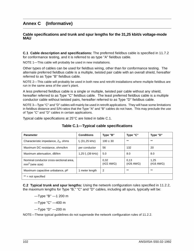
Annex C (Informative)
Cable specifications and trunk and spur lengths for the 31,25 kbit/s voltage-mode MAU
C.1 Cable description and specifications: The preferred fieldbus cable is specified in 11.7.2 for conformance testing, and it is referred to as type "A" fieldbus cable.
NOTE 1—This cable will probably be used in new installations.
Other types of cables can be used for fieldbus wiring, other than for conformance testing. The alternate preferred fieldbus cable is a multiple, twisted pair cable with an overall shield, hereafter referred to as Type "B" fieldbus cable.
NOTE 2—This cable will probably be used in both new and retrofit installations where multiple fieldbus are run in the same area of the user's plant.
A less preferred fieldbus cable is a single or multiple, twisted pair cable without any shield, hereafter referred to as Type "C" fieldbus cable. The least preferred fieldbus cable is a multiple conductor cable without twisted pairs, hereafter referred to as Type "D" fieldbus cable.
NOTE 3—Type "C" and "D" cables will mainly be used in retrofit applications. They will have some limitations in fieldbus distance and S/N ratios that the Type "A" and "B" cables do not have. This may preclude the use of Type "C" and "D" cables in certain applications.
Typical cable specifications at 25°C are listed in table C.1.
Table C.1—Typical cable specifications
C.2 Typical trunk and spur lengths: Using the network configuration rules specified in 11.2.2, the maximum lengths for Type "B," "C" and "D" cables, including all spurs, typically will be:
—Type "B" —1 200 m
—Type "C" —400 m
—Type "D" —200 m
NOTE—These typical guidelines do not supersede the network configuration rules of 11.2.2.
Parameter Conditions Type "B" Type "C" Type "D"
Characteristic impedance, Z0, ohms fr (31,25 kHz) 100 ± 30 ** **
Maximum DC resistance, ohms/km per conductor 56 132 20
Maximum attenuation, dB/km 1,25 fr (39 kHz) 5.0 8.0 8.0
Nominal conductor cross-sectional area,
mm2 (wire size)
0,32 (#22 AWG)
0,13(#26 AWG)
1,25 (#16 AWG)
Maximum capacitive unbalance, pF 1 meter length 2 ** **
** = not specified
102 ANSI/ISA-S50.02-1992

Allowable spur lengths for either bus or tree topology are dependent on the number of communication elements on the fieldbus. Table C.2 relates the recommended number of communication elements to spur length. Maximum spur lengths are the same for Type "A," "B," "C," and "D" cables. The table assumes one communication element per spur. When a spur with passive trunk coupler has more than one communication element, the length of that spur should be reduced by 30 m per communication element. As the recommended maximum total spur length is 120 m, the maximum number of communication elements per spur should be 4.
Table C.2—Recommended maximum spur lengths vs. number of communication elements
Spurs of length less than 1 m should be regarded as splices.
Total number of communication elements Recommended maximum spur length, m
25-32 0
19-24 30
15-18 60
13-14 90
1-12 120
ANSI/ISA-S50.02-1992 103


Developing and promulgating technically sound consensus standards, recommended practices, and technical reports is one of ISA's primary goals. To achieve this goal the Standards and Practices Department relies on the technical expertise and efforts of volunteer commi ttee members, chairmen, and reviewers.
ISA is an American National Standards Institute (ANSI) accredited organization. ISA administers United States Technical Advisory Groups (USTAGs) and provides secretariat support for International Electrotechnical Commission (IEC) and International Organization for Standardization (ISO) committees that develop process measurement and control standards. To obtain additional information on the Society's standards program, please write:
ISAAttn: Standards Department67 Alexander DriveP.O. Box 12277Research Triangle Park, NC 27709
ISBN: 1-55617-317-2