Embed Size (px)
Citation preview
LA BARBERA ET AL. VOL. XXX ’ NO. XX ’ 000–000 ’ XXXX
www.acsnano.org
A
CXXXX American Chemical Society
Filamentary Switching: SynapticPlasticity through Device VolatilitySelina La Barbera, Dominique Vuillaume, and Fabien Alibart*
Institut d'Electronique, Microelectronique et Nanotechnologies, UMR-CNRS 8520, 59652 Villeneuve d'Ascq Cedex, France
Massive amounts of heterogeneousdata are generated each day in oursociety. In this context, computing
systems face important challenges inproviding suitable solutions for informa-tion processing. Saturation of conventionalcomputer performances due to materialissues (i.e., clock frequency and energylimitations) and more fundamental con-straints inherent in the Von Neumannbottleneck have forced researchers to in-vestigate new computing paradigms thatwill allow for more powerful systems. Thebioinspired approach (or, more precisely,neuromorphic engineering) is a promisingdirection for such an objective. Recentbreakthroughs at the system,1 circuit,2 anddevice levels3 are very encouraging indica-tors for the development of computingsystems that can replicate the brain's per-formances in tasks such as recognition,mining, and synthesis.4 To achieve such anambitious goal, research efforts are neededfor understanding the computing principlesof biological systems, elucidating how
spike-coding information is computed andstored in neuron and synapse assemblies,and exploring neuromorphic approachesthat define hardware functionalities, perfor-mances, and integration requirements.Emerging nanotechnologies could playa major role in this context, by offeringdeviceswith attractive bioinspired function-alities and associated performances thatwould ensure the future development ofneuromorphic hardware.Some studies have investigated the pos-
sibility of implementing neurons in nano-scale devices.5,6 Most of these efforts havebeen devoted to the realization of synapticelements with emerging memory devices,such as RRAM technologies, with the goalsof matching the critical integration densityof the synaptic connections7 and replicatingthe synaptic plasticity mechanisms thatcorrespond to the modification of synapticconductance during learning and comput-ing. Indeed, modification of the synapticweight as a function of neuronal activity(i.e., spiking activity) is widely recognized as
* Address correspondence [email protected].
Received for review November 26, 2014and accepted January 12, 2015.
Published online10.1021/nn506735m
ABSTRACT Replicating the computational functionalities and performances of the
brain remains one of the biggest challenges for the future of information and
communication technologies. Such an ambitious goal requires research efforts from
the architecture level to the basic device level (i.e., investigating the opportunities
offered by emerging nanotechnologies to build such systems). Nanodevices, or, more
precisely, memory or memristive devices, have been proposed for the implementation of
synaptic functions, offering the required features and integration in a single component.
In this paper, we demonstrate that the basic physics involved in the filamentary
switching of electrochemical metallization cells can reproduce important biological
synaptic functions that are key mechanisms for information processing and storage. The transition from short- to long-term plasticity has been reported as
a direct consequence of filament growth (i.e., increased conductance) in filamentary memory devices. In this paper, we show that a more complex filament
shape, such as dendritic paths of variable density and width, can permit the short- and long-term processes to be controlled independently. Our solid-state
device is strongly analogous to biological synapses, as indicated by the interpretation of the results from the framework of a phenomenological model
developed for biological synapses. We describe a single memristive element containing a rich panel of features, which will be of benefit to future
neuromorphic hardware systems.
KEYWORDS: memristive device . electrochemical metallization cell . filamentary switching . synaptic plasticity .neuromorphic computing
ARTIC
LE
LA BARBERA ET AL. VOL. XXX ’ NO. XX ’ 000–000 ’ XXXX
www.acsnano.org
B
a key mechanism for the processing and storage ofinformation in neural networks.Plasticity mechanisms are commonly categorized
as short- and long-term plasticity (STP and LTP,respectively). STP corresponds to a neuronally inducedsynaptic weight modification that tends to relaxtoward a resting state, thereby providing activity-dependent signal processing. In LTP, the synapticweight modification can last for days to months. Thus,LTP provides the information storage capability to thenetwork. Spike timing-dependent plasticity is a varia-tion of Hebb's rule8,9 that has attracted a lot of atten-tion. Although not involved in all mechanisms oflearning, spike timing-dependent plasticity has beendemonstrated in various nanoscale memory or mem-ristive devices.10�17 Other important expressions ofplasticity that have been displayed in memristivesystems include STP,18,19 demonstrated based onthe volatile memory effect, and the STP to LTPtransition,20�23 displayed in filamentary memorydevices in which electrical conductivity is modulatedby growth of a conductive filament. Conductive fila-ment growth is induced by the accumulation of elec-trical stress and leads to an increase in deviceconductivity. By analogy to long-term memorizationprocesses, which involve the accumulation of short-term effects, and to the idea of reinforcementlearning,24 conductive filament growth has beendirectly correlated with increased filament stability,corresponding to long-term storage of the conductivestate. In these differentworks, while the strong analogybetween biological synapses and nanoscale filamen-tary memory devices is evidenced, transition betweenSTP and LTP is intrinsic to the material system con-sidered (i.e., ionic species, ionic conductor) and cannotbe controlled and tuned during operation.In this paper, we demonstrate that more complex
plastic behaviors can emerge from nanoscale memris-tive devices, thus allowing a greater number offeatures to be embedded in a single component and
potentially permitting more complex computingsystems. By considering more complex filamentshapes, such as dendritic metallic paths of differentbranch densities andwidths, we show that the volatile/nonvolatile regime can be tuned independently, lead-ing to an independent control of STP and LTP.On the basis of the observation of metallic filaments
in macroscale electrochemical metallization (ECM)cells, we investigated the growth and stability proper-ties of dendritic filaments. The results were used as abasis for the development of nanoscale solid-statesynapses that display independent control of STPand LTP processes via spiking excitation and pasthistory modification. When this behavior was inter-preted from the framework of the phenomenologicalmodeling developed for synaptic plasticity, the resultsrevealed a strong analogy between our solid-statedevice and biological synapses. The additional function-ality of independent control of STP and LTPcould lead tonew learning and computing strategies for neuro-morphic engineering and artificial neural networks.
RESULTS AND DISCUSSION
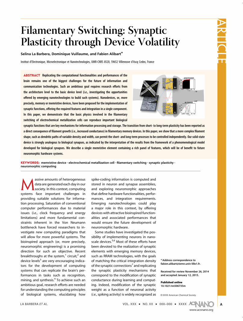
Ag2S Filamentary Switching. The basic structure of thesynaptic device (Figure 1a) corresponds to a conven-tional ECM cell, as described by Waser.25 Inert andreactive Pt and Ag electrodes, respectively, are sepa-rated by a Ag2S ionic conductor material (60 nm),which ensures the migration of oxidized Agþ ionsbetween the electrodes. A positive bias (with agrounded Pt electrode) induces the oxidation of Aginto Agþ ions at the Ag electrode, themigration of ionsfrom theAg anode to the Pt cathode, and the reductionof Agþ ions into Ag filaments across the insulatingAg2S, thereby turning the device from an insulatingOFF state to a conductive ON state (SET transition).A negative bias induces the oxidation of Ag fromthe filament into Agþ ions and reduction at the Agelectrode, leading to a disruption of the conductivepath that turns the device OFF (RESET transition).
Figure 1. Filamentary switching. (a) Basic switching mechanism of ECM cells. (b) Device configuration at the millimeter scale(top: 0.1 mm � 0.1 mm active area) and nanometer scale (bottom: 200 nm � 200 nm cross-point active area).
ARTIC
LE
LA BARBERA ET AL. VOL. XXX ’ NO. XX ’ 000–000 ’ XXXX
www.acsnano.org
C
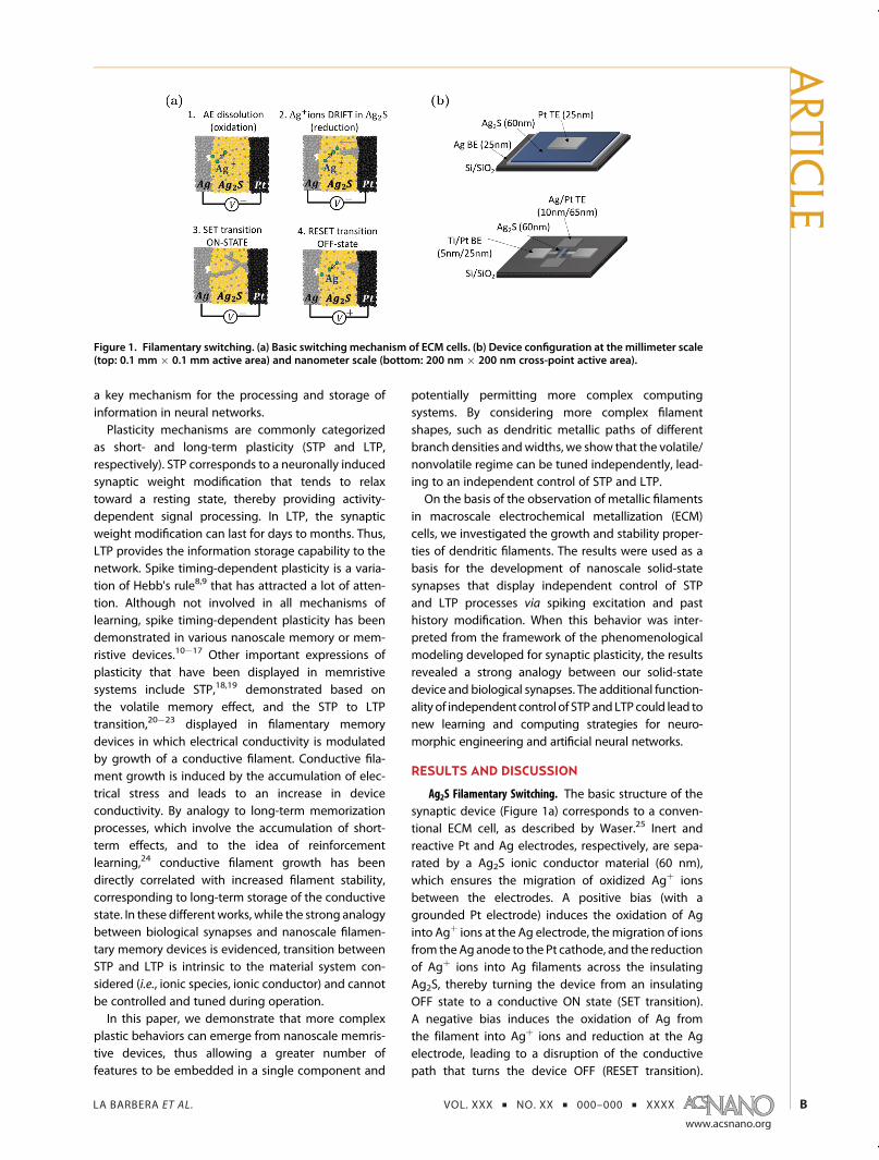
To gain insight into the filament shape and growthmechanism, we performed optical microscopic ima-ging during the current�voltage (I�V) measurementon millimeter-scale devices with a square-shaped Ptelectrode on top of a Ag/Ag2S substrate (Figure 1b).
Consistent with the switching scenario describedabove, a positive bias induced the formation of Agdendritic filaments from the Pt cathode toward the Aganode (SET transition, Figure 2a, snapshot 1 to 3).Application of a negative bias induced a partialdestruction of the conducting paths, with remainingfilament traces corresponding to preferential paths forsubsequent switching (RESET transition, Figure 2a,snapshot 4). After an identical positive SET transition,an intermediate situation was observed, in which thedevice was kept grounded for 5 min with a slowdissolution of the metallic dendrites (Figure 2a, snap-shot 4*). Such filament relaxation can be attributed tothe Agþ ion diffusion in the Ag2S ionic conductor andto the reverse oxidation�reduction process of the Agfilaments.26
A second analysis of the filament formation wasrealized by varying the compliance current (Ic) duringthe SET process. This approach is commonly usedin ECM cells to tune the conductance of the ON stateand to limit the formation of filaments.27 If tuningthe conductance by limiting the growth of a singlefilament is considered straightforward (i.e., becausethe filament diameter corresponds directly to theconductance state), then a more complex picture wasobtained for ECM cells that had complex dendritic
filamentmorphologies. Increasing the density or widthof the dendritic branch can correspond to an increaseof conductance. Because of the resolution of theoptical microscope, it was not possible to obtain anaccurate assessment of filament diameter. However,we effectively measured a larger filament expansionand dendritic tree density with a larger Ic (Figure 2c).This observation indicates a direct correlation betweenIc and the fractal geometry of the dendritic filaments(see Supporting Information, Figure S1). Again, afterRESET, the remaining filament traces corresponded topreferential paths for subsequent switching.
Using the previous analysis as a guideline fordescribing nanoscale filament stability, we implemen-ted the same structure in nanoscale devices consistingof Ag/Pt cross-points with a 200 nm � 200 nm activearea separated by Ag2S (Figure 1b). This device con-figuration offers the potential for cross-bar integration(cross-point of metallic wires) and for the realization ofdense synaptic arrays. Because of the high mobility ofthe Agþ ions in the Ag2S ionic conductor, the devicewas operated at low voltages, close to the biologicalelectrical potential recorded in neuronal cells duringspiking (200 vs 80 mV).
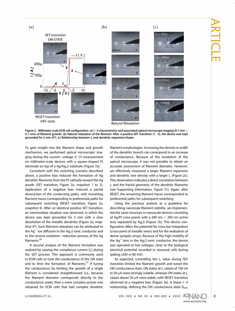
As expected, controlling the Ic value during SETtransition limited the filament growth and tuned theON conductance state. ON states at Ic values of 100 nAto 50 μA were strongly volatile, whereas ON states at Icvalues above 50 μA were stable, with RESET transitionobserved at a negative bias (Figure 3a). A linear I�V
relationship, defining the ON conductance state GON,
Figure 2. Millimeter-scale ECM cell configuration. (a) I�V characteristics and associated optical microscope imaging (0.1 mm�0.1 mm) of filament growth. (b) Natural relaxation of the filament. After a positive SET transition (1�3), the device was keptgrounded for 5 min (4*). (c) Relationship between Ic and dendritic expansion/shape.
ARTIC
LE
LA BARBERA ET AL. VOL. XXX ’ NO. XX ’ 000–000 ’ XXXX
www.acsnano.org
D
was obtained in all ON states, indicating that thefilaments bridged the gap between the electrodes.Consequently, the large dynamic range of ON statespresented in Figure 3b, namely, from high resistance atlow Ic (i.e., 1 MΩ at 100 nA, corresponding to a switch-ing power <100 nW), to low resistance at high Ic(i.e., 1kΩ at 1 mA, corresponding to a switching powerof 300 μW) can be attributed to a modification of thebridging filament morphology, rather than to a mod-ulation of the tunnel barrier length (which is a plausiblemechanism in the case of a nonbridging filament).
As a first level of interpretation, the low Ic region canbe reasonably described by weak filaments that tendto dissolve very quickly once the voltage is removed.The high Ic region can be considered to correspond tostrong bridging filaments with slower relaxation. Thiseffect has been described thermodynamically in Agfilaments28 as a competition between the surface andvolume energies: thin filaments tend to be disruptedbecause the surface energy is higher than the volumeenergy, whereas thick filaments tend to stabilize be-cause the volume energy is higher than the surfaceenergy. Such relaxation of the conductive paths hasbeen reported in nanoscale devices22,23 and was thebasis for the implementation of STP and the STP to LTPtransition. After the conductive filament forms via astrong stimulation, the filaments tend to dissolve andthe device relaxes toward its insulating state, leadingto STP behavior. Stronger stimulation of the device
during the SET transition leads to stronger filamentsand higher conductance states with more stable char-acteristics, resulting in LTP. In this case, the conduc-tance state is correlated directly with the volatility.
Assuming that similar dendritic processes occur atthe nanometer and millimeter scales (Figure 2a), wecan draw amore complex picture for the interpretationof filament stability. Specifically, the different ON statescan be described by dendritic trees, in which theresistance is modulated equally by the density anddiameter of the branches. At the nanoscale, the sameON state can be obtained by filaments with dense andthin branches as can be obtained by filaments with lessdense and thick branches (Figure 3c). Both configura-tions should lead to different volatilities, emulatingdifferent plasticity properties.
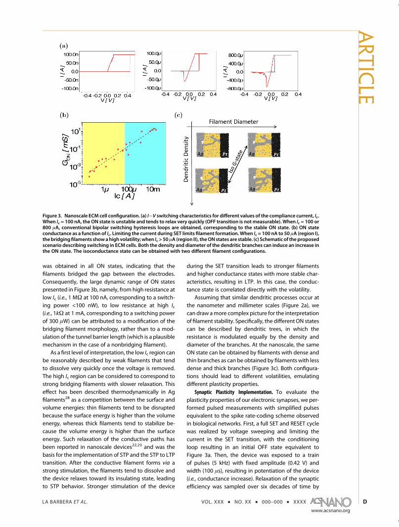
Synaptic Plasticity Implementation. To evaluate theplasticity properties of our electronic synapses, we per-formed pulsed measurements with simplified pulsesequivalent to the spike rate-coding scheme observedin biological networks. First, a full SET and RESET cyclewas realized by voltage sweeping and limiting thecurrent in the SET transition, with the conditioningloop resulting in an initial OFF state equivalent toFigure 3a. Then, the device was exposed to a trainof pulses (5 kHz) with fixed amplitude (0.42 V) andwidth (100 μs), resulting in potentiation of the device(i.e., conductance increase). Relaxation of the synapticefficiency was sampled over six decades of time by
Figure 3. Nanoscale ECM cell configuration. (a) I�V switching characteristics for different values of the compliance current, Ic.When Ic = 100 nA, the ON state is unstable and tends to relax very quickly (OFF transition is not measurable). When Ic = 100 or800 μA, conventional bipolar switching hysteresis loops are obtained, corresponding to the stable ON state. (b) ON stateconductance as a function of Ic. Limiting the current during SET limits filament formation.When Ic = 100 nA to 50 μA (region I),thebridgingfilaments showahigh volatility;when Ic > 50μA (region II), theON states are stable. (c) Schematic of the proposedscenario describing switching in ECM cells. Both the density and diameter of the dendritic branches can induce an increase inthe ON state. The isoconductance state can be obtained with two different filament configurations.
ARTIC
LE
LA BARBERA ET AL. VOL. XXX ’ NO. XX ’ 000–000 ’ XXXX
www.acsnano.org
E
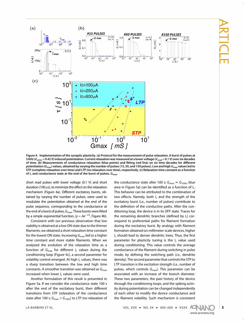
short read pulses with lower voltage (0.1 V) and shortduration (100μs), tominimize the effect on the relaxationmechanism (Figure 4a). Different excitatory bursts, ob-tained by varying the number of pulses, were used tomodulate the potentiation obtained at the end of thepulse sequence, corresponding to the conductance attheendof aburst of pulses,Gmax. Theseburstswere fittedby a simple exponential function, (y = Ae�x/t, Figure 4b).
Consistent with our previous observation that lowstability is obtained at a lowON state due to the thinnerfilaments, we obtained a short relaxation time constantfor the lowest ON state. Increasing Gmax led to a highertime constant and more stable filaments. When weanalyzed the evolution of the relaxation time as afunction of Gmax for different Ic values during theconditioning loop (Figure 4c), a second parameter forvolatility control emerged. At high Ic values, there wasa sharp transition between the low and high timeconstants. A smoother transition was obtained as Gmax
increased when lower Ic values were used.Another formulation of this result is presented in
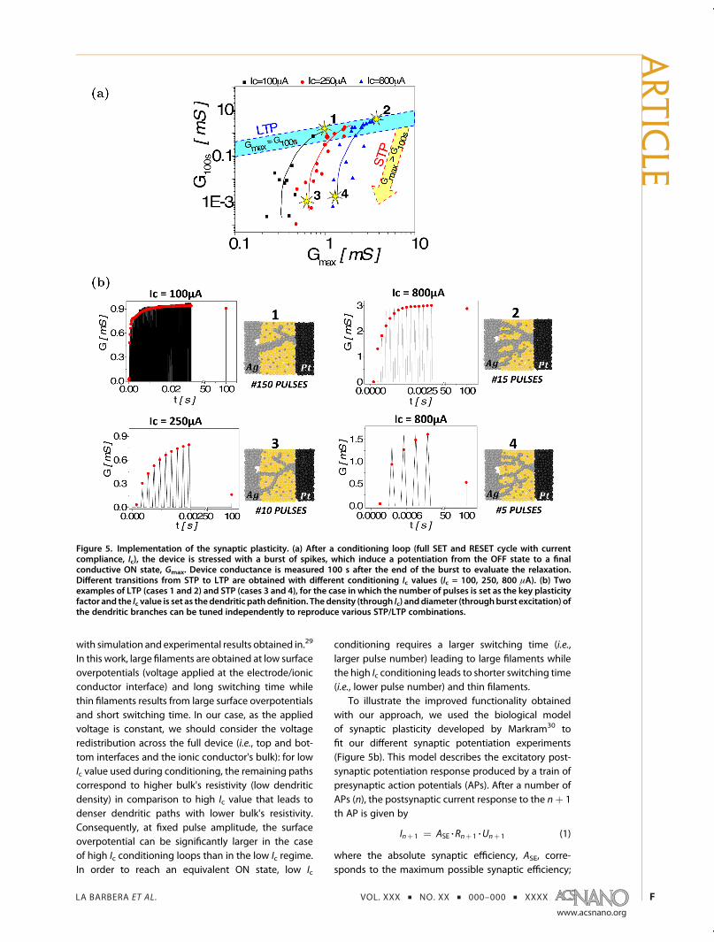
Figure 5a. If we consider the conductance state 100 safter the end of the excitatory burst, then differenttransitions from STP (relaxation of the conductancestate after 100 s; Gmax > G100s) to LTP (no relaxation of
the conductance state after 100 s; Gmax = G100s, bluearea in Figure 5a) can be identified as a function of Ic.This behavior can be attributed to the combination oftwo effects. Namely, both Ic and the strength of theexcitatory burst (i.e., number of pulses) contribute tothe definition of the conductive paths. After the con-ditioning loop, the device is in its OFF state. Traces forthe remaining dendritic branches (defined by Ic) cor-respond to preferential paths for filament formationduring the excitatory burst. By analogy with filamentformation obtained onmillimeter-scale devices, higherIc should lead to denser dendritic trees. Thus, the firstparameter for plasticity tuning is the Ic value usedduring conditioning. This value controls the averageconductance of the filament during switching in pulsemode, by defining the switching path (i.e., dendritedensity). The secondparameter that controls the STP toLTP transition is the excitation strength (i.e., number ofpulses, which controls Gmax). This parameter can beassociated with an increase of the branch diameter.These two parameters, the past history of the devicethrough the conditioning loops, and the spiking activ-ity during potentiation can be changed independentlyof each other to modify the device conductance andthe filament volatility. Such mechanism is consistent
Figure 4. Implementation of the synaptic plasticity. (a) Protocol for themeasurement of pulse relaxation. A burst of pulses at5 kHz (Vwrite = 0.42 V) inducedpotentiation. Current relaxationwasmeasured at a lower voltage (Vread = 0.1 V) over six decadesof time. (b) Measurements of conductance relaxation (blue points) and fitting (red line) on six time decades for differentpotentiation (Gmax) values, obtainedby varying the number of pulses (15, 50, and 150pulses). LowandhighGmax values led toSTP (complete relaxation over time) and LTP (no relaxation over time), respectively. (c) Relaxation time constant as a functionof Ic and conductance state at the end of the burst of pulses, Gmax.
ARTIC
LE
LA BARBERA ET AL. VOL. XXX ’ NO. XX ’ 000–000 ’ XXXX
www.acsnano.org
F
with simulation and experimental results obtained in.29
In this work, large filaments are obtained at low surfaceoverpotentials (voltage applied at the electrode/ionicconductor interface) and long switching time whilethin filaments results from large surface overpotentialsand short switching time. In our case, as the appliedvoltage is constant, we should consider the voltageredistribution across the full device (i.e., top and bot-tom interfaces and the ionic conductor's bulk): for lowIc value used during conditioning, the remaining pathscorrespond to higher bulk's resistivity (low dendriticdensity) in comparison to high Ic value that leads todenser dendritic paths with lower bulk's resistivity.Consequently, at fixed pulse amplitude, the surfaceoverpotential can be significantly larger in the caseof high Ic conditioning loops than in the low Ic regime.In order to reach an equivalent ON state, low Ic
conditioning requires a larger switching time (i.e.,larger pulse number) leading to large filaments whilethe high Ic conditioning leads to shorter switching time(i.e., lower pulse number) and thin filaments.
To illustrate the improved functionality obtainedwith our approach, we used the biological modelof synaptic plasticity developed by Markram30 tofit our different synaptic potentiation experiments(Figure 5b). This model describes the excitatory post-synaptic potentiation response produced by a train ofpresynaptic action potentials (APs). After a number ofAPs (n), the postsynaptic current response to the nþ 1th AP is given by
Inþ 1 ¼ ASE 3 Rnþ 1 3Unþ 1 (1)
where the absolute synaptic efficiency, ASE, corre-sponds to the maximum possible synaptic efficiency;
Figure 5. Implementation of the synaptic plasticity. (a) After a conditioning loop (full SET and RESET cycle with currentcompliance, Ic), the device is stressed with a burst of spikes, which induce a potentiation from the OFF state to a finalconductive ON state, Gmax. Device conductance is measured 100 s after the end of the burst to evaluate the relaxation.Different transitions from STP to LTP are obtained with different conditioning Ic values (Ic = 100, 250, 800 μA). (b) Twoexamples of LTP (cases 1 and 2) and STP (cases 3 and 4), for the case in which the number of pulses is set as the key plasticityfactor and the Ic value is set as thedendritic path definition. Thedensity (through Ic) anddiameter (throughburst excitation) ofthe dendritic branches can be tuned independently to reproduce various STP/LTP combinations.
ARTIC
LE
LA BARBERA ET AL. VOL. XXX ’ NO. XX ’ 000–000 ’ XXXX
www.acsnano.org
G
the fraction of available synaptic resources, R, corre-sponds to the neurotransmitter resources that areavailable in the presynaptic connection (0 < R < 1);and the utilization of the synaptic efficacy, U, cor-responds to the amount of neurotransmitter that isreleased from the pre- to the postsynaptic connection(0 < U < 1). Thus, Rnþ1 and Unþ1 are given by
Rnþ 1 ¼ Rn(1 � Unþ 1)e�Δt=τrec þ (1 � e�Δt=τrec )
Unþ 1 ¼ Une�Δt=τfac þUSE(1 � Un)e�Δt=τfac )
((2)
The facilitating behavior observed during a burst ofspikes is associated with the parameter USE, which ismodified with the characteristic time τfac and appliedto the first AP in a train (i.e., R1 = 1 � USE). Recovery ofthe synaptic efficiency (or available neurotransmitters)is associated with the characteristic time τrec. Thisbiological model allows us to reproduce different kindsof plasticity observed in synapses relative to differentmechanisms. Plasticity can be controlled through theneurotransmitter dynamics in the presynaptic connec-tion (i.e., recovery of the available neurotransmitters orincrease in the neurotransmitter release probability),by the improvement of neurotransmitter detection inthe postsynaptic connection or even by a structuralmodification of the synaptic connection (i.e., increasein the size of a given synapse or the overall number ofsynapses connecting two neurons). For a detailedreview of synaptic plasticity, see refs 31 and 32. Con-sequently, the synaptic efficiency of a given spike isdetermined by a combination of parameters that leadto different synaptic responses and expressions ofsynaptic plasticity.
By accounting for the parameters of the biomodel(eq 2), four different cases may be analyzed as afunction of the number of pulses and Ic (Table 1). Ifwe consider experiments 1 and 3 in Figure 5b, the samepotentiation (i.e., Gmax = 0.9 mS) can lead to LTP (case1with 150 pulses and Ic = 100 μA) or STP (case 3with 10pulses and Ic = 250 μA). The STP to LTP transition ismainly associated with an increase of the facilitatingtime constant, τfac. This increase is obtained by increas-ing the number of pulses during the excitatory burst.
Slightly increasing Ic is mostly represented by anincrease in ASE. This observation is also evident bycomparing case 2 with case 4. The difference in con-ductance level between cases 1 and 2, which showedqualitatively equivalent LTP responses, is mainly attrib-uted to an increase of ASE, from 6 mS (case 1) to 25 mS(case 2). We cannot establish a one-to-one correspon-dence between biological processes (e.g., neurotrans-mitter dynamics, structural modifications, etc.) andfilament growth or relaxation in our experiments be-causemost of the parameters are coupled in both cases.Additional experiments, such as the in situ observationof filament shape, would providemore insights in orderto formulate of more refined equivalence.
DISCUSSION
Obtaining the synaptic density has been a majorchallenge in neuromorphic engineering. From a prac-tical perspective, we believe that developing devicesthat are more functional (i.e., have properties closer tobiological synapses) will allow the construction ofmorecomplex systems. In a previous report describing theSTP to LTP transition,14,22 the transition was controlledby a single parameter (i.e., device conductance). Suchbehavior was proposed as a direct solution for theimplementation of the multistore memory model33
which considers that learning events contribute tothe formation of short-termmemory (wherememory isused in the sense of psychology) before being trans-ferred into long-term memory (STM/LTM transition). Ifa direct equivalence between STP/LTP and STM/LTM isnot straightforward, it seems realistic to consider sy-naptic plasticity as a key element in the formation ofmemory. The device presented in this paper features atunable STP/LTP transition that could be a key param-eter for defining the appropriate activity threshold thatdetermines when information storage needs to bemoved from a short-term to a long-term regime, or,in other words, how long an information needs tobe sustained (i.e., how long the device will remain in itsON state).Additionally, if STP/LTP transition is only controlled
by the device's conductance, synaptic weight modifi-cation and STP/LTP transition cannot be uncorrelated.We argue that the rate-coding property obtained in theSTP regime, as observed in the facilitation of synapticsignal transmission during a high frequency burst ofspikes and the subsequent relaxation at lower frequen-cies, disappears once the device enters into its LTPregime and, thus, becomes a linear resistor. From acircuit perspective, if we consider a simple integrate-and-fire neuron associated with linear synapses, thenode (neuron and synapses) is equivalent to a simplelinear filter (if the variable is the average spiking rate).The node is a nonlinear filter in the STP regime withfrequency-dependent synaptic conductance. Theoverall network functionality is reduced when learning
TABLE 1. Fitting Parameters Used for Synaptic Plasticity
Modeling
LTP STP
case 1 case 2 case 3 case 4
Ic = 100 μA Ic = 800 μA Ic = 250 μA Ic = 800 μA
150 pulses 15 pulses 10 pulses 5 pulsesUSE = 0.0279 USE = 0.0279 USE = 0.0251 USE = 0.0279ASE = 6 mS ASE = 25 mS ASE = 6.5 mS ASE = 16 mSτrec = 0.0013 s τrec = 0.0013 s τrec = 0.0010 s τrec = 0.0012 sτfac = 11.5500 s τfac = 18.5500 s τfac = 0.0150 s τfac = 1.5500 s
ARTIC
LE
LA BARBERA ET AL. VOL. XXX ’ NO. XX ’ 000–000 ’ XXXX
www.acsnano.org
H
moves synapses from their STP to their LTP domain. Aninteresting property offered by the presented devicesin order to preserved such rate coding functionality isto allow for weight modification through the control ofthe ASE parameter while maintaining the frequencydependent response by keeping the device into itsshort-term regime (see case 3 and 4, Figure 5). For thedevice presented in this paper, learning can be realizedby modifying the dendritic filament density andincreasing the ASE during the conditioning procedure.The frequency coding property can be ensured bycontrolling the filament diameter and relaxation.Finally, the activity dependent STP/LTP transition
and synaptic weight modification in this work is onlyobtained as a function of the input frequency, thuscorresponding to the preneuron activity. Such me-chanism is defined in biology as a facilitating synapse.A complementary mechanism, that cannot be repro-duce with our system, is the depressing synapse (i.e.,decrease of the synaptic weight when preneuronactivity increase). In order to implement practicallearning systems, these results will have to beextended to hebbian learning strategies in whichweight modification is dependent on both pre- andpostneuron activity. Among the different hebbianlearning strategies considered to date, STDP has at-tracted a large attention. One implementation of suchlearning protocol is based on overlapping pulses (spiketiming difference between pre- and postneuron is thenencoded as a voltage drop across the device). Figure S3presents similar results to Figure 5 when voltage isused as a key plasticity factor instead of spikingfrequency that should allow for STDP realization. While
not measured in this paper, one interesting futuredirection would be to add to previously reported STDPresults obtained on nonvolatile systems11 the STP/LTPcapacity in order to demonstrate neuromorphic cir-cuits with richer dynamical behaviors.
CONCLUSIONS
We report a single synaptic device that highly resem-bles its biological counterpart, opening thefield tomorecomplex neuromorphic systems. Biological synapticplasticity has been successfully implemented in ournanoscale memristive device by considering the fila-ment stability of ECM cells, in terms of competitionbetween the density and diameter of the dendriticbranches. STP and LTP regimes can be controlled bytuning the device volatility. The first parameter forplasticity tuning, Ic, is used during conditioning andcontrols the average conductance of the filament dur-ing switching in pulse mode. The second parameterhandles the STP to LTP transition and corresponds to theexcitation strength (number of pulses), which controlsGmax. The second parameter can be associated with anincrease of the branch diameter. These two parameterscan be tuned independently of each other tomodify thedevice conductance and filament volatility.Future work should investigate how such synaptic
properties can be advantageous for large-scale neuro-morphic circuits. To improve the efficiency of futurebioinspired computing systems, interdisciplinary re-search is needed to obtain a better understanding ofthe contributions of STP and LTP mechanisms tomemory construction and spike-coding informationprocessing.
METHODSDevice Structure and Fabrication. To fabricate the millimeter-
scale Ag/Ag2S/Pt device (Figure 1b), a 25 nm Ag bottomelectrode was deposited by direct current magnetron sputter-ing onto the cleaned surface of p-type silicon, which wascovered with thermally grown 200 nm thick SiO2 at roomtemperature. A thin film of Ag2S (60 nm) was deposited bythermal evaporation onto the full substrate. Finally, a Pt topelectrode, with a thickness of 25 nm and electrode size of 1mm,was deposited on the Ag2S layer by using a shadow mask anddirect current magnetron sputtering. To fabricate the nanoscaledevice, a 5 nm/25 nm Ti/Pt bottom electrode was deposited atroom temperature on thermally grown SiO2 (200 nm) andpatterned via lift-off and electron beam lithography (EBL). Athin film of Ag2S (60 nm) was deposited by thermal evaporationand patterned via lift-off and EBL. Finally, a 10 nm/70 nm Ag/Pttop electrode was deposited on the Ag2S by direct currentmagnetron sputtering and patterned via lift-off and EBL.
Characterization of the Switching Dynamics. The electrical char-acteristics of the device, the waveform design of the pulses atfixed amplitude (Vwrite = 0.4 V and Vread = 0.1 V) and width(w = 100 μs), and the pulse measurements were obtained byusing a semiconductor device analyzer (B1500A, Agilent) and awaveform function generator (WGFMU B1530A, Agilent), whichwere piloted in remote mode by VISUAL STUDIO. For allmeasurements, the device electrodes were contacted with amicromanipulator probe-station (Suss Microtec PM-5), and the
Pt electrode was grounded. Conditioning loops, characterizedby a full SET and RESET cycle, were realized by sweeping voltageand limiting current in the SET transition.
Conflict of Interest: The authors declare no competingfinancial interest.
Acknowledgment. The authors thank D. Guerin, F. Vaurette,S. Lenfant for technical expertises and D. Querlioz for carefulreading of themanuscript. This work was supported by the ANRDINAMO project (no. ANR-12-PDOC-0027-01).
Supporting Information Available: Fractal analysis of thedendritic filaments and implementation of the synaptic plasti-city with the pulse amplitude as the key plasticity factor.This material is available free of charge via the Internet athttp://pubs.acs.org.
REFERENCES AND NOTES1. Merolla, P. A.; Arthur, J. V.; Alvarez-Icaza, R.; Cassidy, A. S.;
Sawada, J.; Akopyan, F.; Jackson, B. L.; Imam, N.; Guo, C.;Nakamura, Y. A Million Spiking-Neuron Integrated Circuitwith a Scalable Communication Network and Interface.Science 2014, 345, 668–673.
2. Alibart, F.; Zamanidoost, E.; Strukov, D. B. Pattern Classifi-cation by Memristive Crossbar Circuits Using Ex Situ and InSitu Training. Nat. Commun. 2013, 4, 403–405.
ARTIC
LE
LA BARBERA ET AL. VOL. XXX ’ NO. XX ’ 000–000 ’ XXXX
www.acsnano.org
I
3. Strukov, D. B.; Snider, G. S.; Stewart, D. R.; Williams, R. S. TheMissing Memristor Found. Nature 2008, 453, 80–83.
4. Liang, B.; Dubey, P. Recognition, Mining and Synthesis.Intel Technol. J. 2005, 9, 99–174.
5. Pickett, M. D.; Medeiros-Ribeiro, G.; Williams, R. S. AScalable Neuristor Built with Mott Memristors. Nat. Mater.2013, 12, 114–117.
6. Sharad, M.; Augustine, C.; Panagopoulos, G.; Roy, K. Spin-based Neuron Model with Domain-wall Magnets asSynapse. IEEE Trans. Nanotechnol. 2012, 11, 843–853.
7. Strukov, D. B. Nanotechnology: Smart Connections.Nature2011, 476, 403–405.
8. Markram, H.; Lübke, J.; Frotscher, M.; Sakmann, B. Regula-tion of Synaptic Efficacy by Coincidence of PostsynapticAPs and EPSPs. Science 1997, 275, 213–215.
9. Hebb, D. The Organization of Behavior: A Neuropsycholo-gical Theory; Psychology Press: New York, 1949; pp 43�56.
10. Bi, G.-q.; Poo, M.-m. Synaptic Modifications in CulturedHippocampal Neurons: Dependence on Spike Timing,Synaptic Strength, and Postsynaptic Cell Type. J. Neurosci.1998, 18, 10464–10472.
11. Jo, S. H.; Chang, T.; Ebong, I.; Bhadviya, B. B.; Mazumder, P.;Lu, W. Nanoscale Memristor Device as Synapse in Neuro-morphic Systems. Nano Lett. 2010, 10, 1297–1301.
12. Kuzum, D.; Jeyasingh, R. G.; Lee, B.; Wong, H.-S. P. Nano-electronic Programmable Synapses Based on PhaseChangeMaterials for Brain-inspired Computing.Nano Lett.2011, 12, 2179–2186.
13. Choi, S.-J.; Kim, G.-B.; Lee, K.; Kim, K.-H.; Yang, W.-Y.; Cho, S.;Bae, H.-J.; Seo, D.-S.; Kim, S.-I.; Lee, K.-J. Synaptic Behaviorsof a Single Metal�Oxide�Metal Resistive Device. Appl.Phys. A 2011, 102, 1019–1025.
14. Kim, K.; Chen, C.-L.; Truong, Q.; Shen, A. M.; Chen, Y. ACarbonNanotube Synapsewith Dynamic Logic and Learn-ing. Adv. Mater. 2013, 25, 1693–1698.
15. Zeng, F.; Li, S.; Yang, J.; Pan, F.; Guo, D. Learning ProcessesModulated by the Interface Effects in a Ti/conductingpolymer/Ti Resistive Switching Cell. R. Soc. Chem. Adv.2014, 4, 14822–14828.
16. Krzysteczko, P.; Münchenberger, J.; Schäfers, M.; Reiss, G.;Thomas, A. The Memristive Magnetic Tunnel Junction as aNanoscopic Synapse-Neuron System. Adv. Mater. 2012,24, 762–766.
17. Alibart, F.; Pleutin, S.; Bichler, O.; Gamrat, C.; Serrano-Gotarredona, T.; Linares-Barranco, B.; Vuillaume, D. AMemristive Nanoparticle/Organic Hybrid Synapstor forNeuroinspired Computing. Adv. Funct. Mater. 2012, 22,609–616.
18. Alibart, F.; Pleutin, S.; Guérin, D.; Novembre, C.; Lenfant, S.;Lmimouni, K.; Gamrat, C.; Vuillaume, D. An Organic Nano-particle Transistor Behaving as a Biological SpikingSynapse. Adv. Funct. Mater. 2010, 20, 330–337.
19. Zhu, L. Q.; Wan, C. J.; Guo, L. Q.; Shi, Y.; Wan, Q. ArtificialSynapse Network on Inorganic Proton Conductor forNeuromorphic Systems. Nat. Commun. 2014, 5, 1–7.
20. Josberger, E. E.; Deng, Y.; Sun, W.; Kautz, R.; Rolandi, M.Two-Terminal Protonic Devices with Synaptic-Like Short-Term Depression and Device Memory. Adv. Mater. 2014,4986–4990.
21. Kim, S.; Choi, S.; Lu, W. Comprehensive Physical Model ofDynamic Resistive Switching in an Oxide Memristor. ACSNano 2014, 8, 2369–2376.
22. Ohno, T.; Hasegawa, T.; Tsuruoka, T.; Terabe, K.; Gimzewski,J. K.; Aono, M. Short-Term Plasticity and Long-Term Po-tentiation Mimicked in Single Inorganic Synapses. Nat.Mater. 2011, 10, 591–595.
23. Yang, R.; Terabe, K.; Liu, G.; Tsuruoka, T.; Hasegawa, T.;Gimzewski, J. K.; Aono, M. On-Demand Nanodevice WithElectrical and Neuromorphic Multifunction Realized byLocal Ion Migration. ACS Nano 2012, 6, 9515–9521.
24. McGaugh, J. L. Memory;a Century of Consolidation.Science 2000, 287, 248–251.
25. Valov, I.; Waser, R.; Jameson, J. R.; Kozicki, M. N. Electro-chemical Metallization Memories Fundamentals, Applica-tions, Prospects. Nanotechnology 2011, 22, 254003.
26. Valov, I.; Linn, E.; Tappertzhofen, S.; Schmelzer, S.; van denHurk, J.; Lentz, F.; Waser, R. Nanobatteries in Redox-BasedResistive Switches Require Extension of Memristor Theory.Nat. Commun. 2013, 4, 1771.
27. Russo, U.; Kamalanathan, D.; Ielmini, D.; Lacaita, A. L.;Kozicki, M. N. Study of Multilevel Programming in Pro-grammable Metallization Cell (PMC) Memory. IEEE Trans.Electron Devices 2009, 56, 1040–1047.
28. Hsiung, C.-P.; Liao, H.-W.; Gan, J.-Y.; Wu, T.-B.; Hwang, J.-C.;Chen, F.; Tsai, M.-J. Formation and Instability of SilverNanofilament in Ag-Based Programmable Metallizationcells. ACS Nano 2010, 4, 5414–5420.
29. Pan, F.; Yin, S.; Subramanian, V. A Detailed Study of theForming Stage of an Electrochemical Resistive SwitchingMemory by KMC Simulation. IEEE Electron Devices Lett.2011, 32, 949–951.
30. Markram, H.; Pikus, D.; Gupta, A.; Tsodyks, M. Potential forMultiple Mechanisms, Phenomena and Algorithms forSynaptic Plasticity at Single Synapses.Neuropharmacology1998, 37, 489–500.
31. Zucker, R. S.; Regehr, W. G. Short-Term Synaptic Plasticity.Annu. Rev. Physiol. 2002, 64, 355–405.
32. Collingridge, G. L.; Peineau, S.; Howland, J. G.; Wang, Y. T.Long-Term Depression in the CNS. Nat. Rev. Neurosci.2010, 11, 459–473.
33. Atkinson, R. C.; Shiffrin, R. M. Human Memory: A ProposedSystem and its Control Processes. Psychol. Learn. Motiv.1968, 2, 89–195.
ARTIC
LE


![XXXX XXXX XXXX XXXX XXXX XXXX 「ShAirDisk2 … XXXX XXXX XXXX XXXX XXXX XXXX XXXX XXXX XXXX XXXX A.「 ShAirDisk2 APP」を起動して[ファイルを開く]をタップすると接続されてい](https://img.pdfslide.net/doc/110x75/5b0631887f8b9a93418c6d6a/xxxx-xxxx-xxxx-xxxx-xxxx-xxxx-shairdisk2-xxxx-xxxx-xxxx-xxxx-xxxx-xxxx-xxxx-xxxx.jpg)