Embed Size (px)
Citation preview
LCD TV
SERVICE MANUALPRODUCT CODE No.1 682 349 45: PAL-BG(TV) DTV
FILE NO.
PRODUCT CODE No.
REFERENCE No.:SM0915100
LCD-46XR10F
CONTENTS
Safety precautions………………………………………………………………………..…
Alignment instructions …………………………….…….…………………………………
Method of software upgrading instructions………………………………………………..
Working principle analysis of the unit……………………………….………….………….
Block diagram…………………………………..………………………………….…………
IC block diagram and instruction…………………………………………………………..……
Wiring diagram …………………………………………………………………………….
Troubleshooting guide ………………………………………………………………..……
Schematic diagram…………………………………………………………………………
APPENDIX-A: Main assembly list
APPENDIX-B: Exploded View
3
5
12
15
18
19
26
27
30
Assemble & Disassemble the Pedestal Base
Wall mounting instructions
Safety precautions 1. Instructions Be sure to switch off the power supply before replacing or welding any components or inserting/plugging in connection wire Anti static measures to be taken (throughout the entire production process!): a) Do not touch here and there by hand at will; b) Be sure to use anti static electric iron; c) It’s a must for the welder to wear anti static gloves. Please refer to the detailed list before replacing components that have special safety requirements. Do not change the specs and type at will. 2. Points for attention in servicing of LCD 2.1 Screens are different from one model to another and therefore not interchangeable. Be sure to use the screen of the original model for replacement. 2.2 The operation voltage of LCD screen is 700-825V. Be sure to take proper measures in protecting yourself and the machine when testing the system in the course of normal operation or right after the power is switched off. Please do not touch the circuit or the metal part of the module that is in operation mode. Relevant operation is possible only one minute after the power is switched off. 2.3 Do not use any adapter that is not identical with the TV set. Otherwise it will cause fire or damage to the set. 2.4 Never operate the set or do any installation work in bad environment such as wet bathroom, laundry, kitchen, or nearby fire source, heating equipment and devices or exposure to sunlight etc. Otherwise bad effect will result. 2.5 If any foreign substance such as water, liquid, metal slices or other matters happens to fall into the module, be sure to cut the power off immediately and do not move anything on the module lest it should cause fire or electric shock due to contact with the high voltage or short circuit. 2.6 Should there be smoke, abnormal smell or sound from the module, please shut the power off at once. Likewise, if the screen is not working after the power is on or in the course of operation, the power must be cut off immediately and no more operation is allowed under the same condition. 2.7 Do not pull out or plug in the connection wire when the module is in operation or just after the power is off because in this case relatively high voltage still remains in the capacitor of the driving circuit. Please wait at least one minute before the pulling out or plugging in the connection wire. 2.8 When operating or installing LCD please don’t subject the LCD components to bending, twisting or extrusion, collision lest mishap should result. 2.9 As most of the circuitry in LCD TV set is composed of CMOS integrated circuits, it’s necessary to pay attention to anti statics. Before servicing LCD TV make sure to take anti static measure and ensure full grounding for all the parts that have to be grounded. 2.10 There are lots of connection wires between parts behind the LCD screen. When servicing or moving the set please take care not to touch or scratch them. Once they are damaged the screen
Attention: This service manual is only for service personnel to take reference with. Before servicing please read the following points carefully.
would be unable to work and no way to get it repaired. If the connection wires, connections or components fixed by the thermotropic glue need to disengage when service, please soak the thermotropic glue into the alcohol and then pull them out in case of dagmage. 2.11 Special care must be taken in transporting or handling it. Exquisite shock vibration may lead to breakage of screen glass or damage to driving circuit. Therefore it must be packed in a strong case before the transportation or handling. 2.12 For the storage make sure to put it in a place where the environment can be controlled so as to prevent the temperature and humidity from exceeding the limits as specified in the manual. For prolonged storage, it is necessary to house it in an anti-moisture bag and put them altogether in one place. The ambient conditions are tabulated as follows:
Temperature Scope for operation 5 ~ +35 oC
Scope for storage -15~ +45 oC
Humidity Scope for operation 20% ~ 80%
Scope for storage <= 80% 2.13 Display of a fixed picture for a long time may result in appearance of picture residue on the screen, as commonly called “ghost shadow”. The extent of the residual picture varies with the maker of LCD screen. This phenomenon doesn’t represent failure. This “ghost shadow” may remain in the picture for a period of time (several minutes). But when operating it please avoid displaying still picture in high brightness for a long time. 3. Points for attention during installation 3.1 The front panel of LCD screen is of glass. When installing it please make sure to put it in place. 3.2 For service or installation it’s necessary to use specified screw lest it should damage the screen. 3.3 Be sure to take anti dust measures. Any foreign substance that happens to fall down between the screen and the glass will affect the receiving and viewing effect 3.4 When dismantling or mounting the protective partition plate that is used for anti vibration and insulation please take care to keep it in intactness so as to avoid hidden trouble. 3.5 Be sure to protect the cabinet from damage or scratch during service, dismantling or mounting.
3 Alignment flow
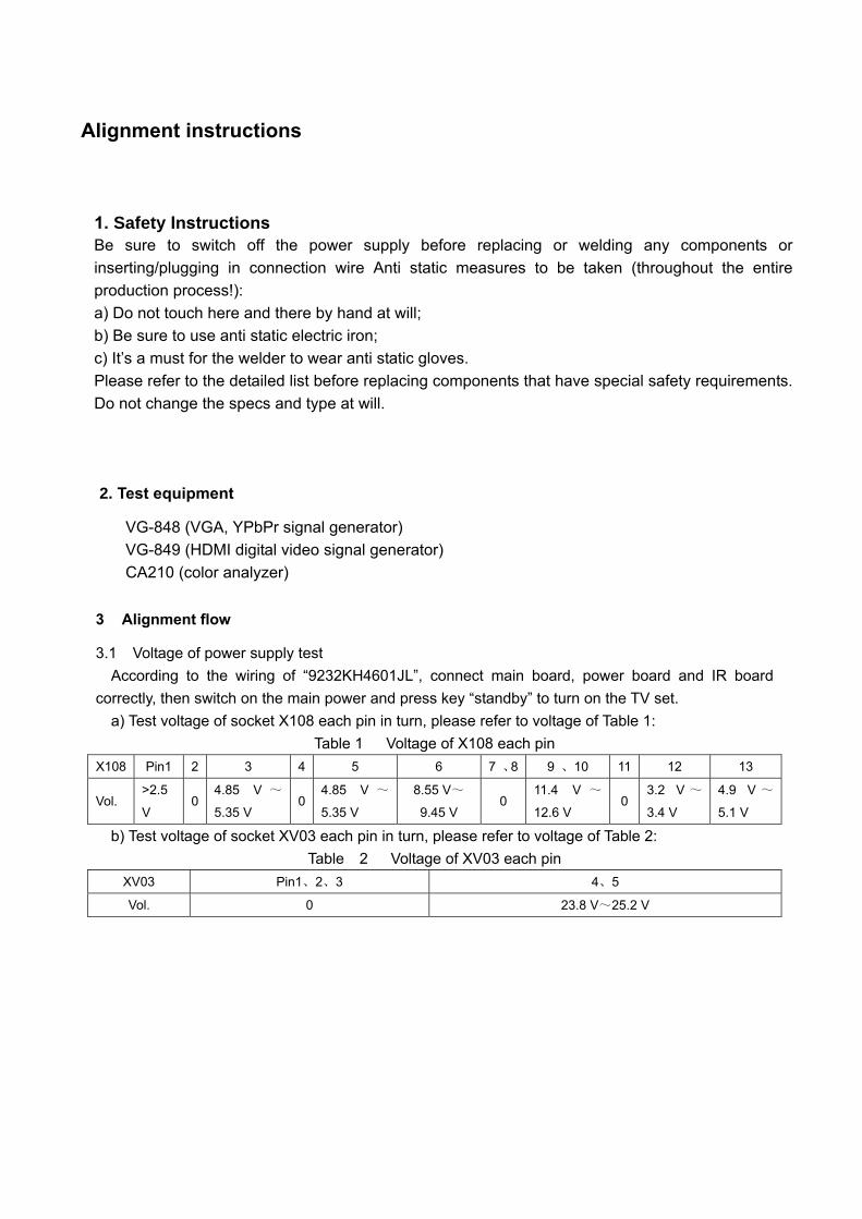
3.1 Voltage of power supply test According to the wiring of “9232KH4601JL”, connect main board, power board and IR board correctly, then switch on the main power and press key “standby” to turn on the TV set. a) Test voltage of socket X108 each pin in turn, please refer to voltage of Table 1:
Table 1 Voltage of X108 each pin X108 Pin1 2 3 4 5 6 7 、8 9 、10 11 12 13
Vol. >2.5
V 0
4.85 V ~
5.35 V 0
4.85 V ~
5.35 V
8.55 V~
9.45 V 0
11.4 V ~
12.6 V 0
3.2 V ~
3.4 V
4.9 V ~
5.1 V
b) Test voltage of socket XV03 each pin in turn, please refer to voltage of Table 2: Table 2 Voltage of XV03 each pin
XV03 Pin1、2、3 4、5
Vol. 0 23.8 V~25.2 V
Alignment instructions
2. Test equipment
VG-848 (VGA, YPbPr signal generator) VG-849 (HDMI digital video signal generator) CA210 (color analyzer)
1. Safety Instructions Be sure to switch off the power supply before replacing or welding any components or inserting/plugging in connection wire Anti static measures to be taken (throughout the entire production process!): a) Do not touch here and there by hand at will; b) Be sure to use anti static electric iron; c) It’s a must for the welder to wear anti static gloves. Please refer to the detailed list before replacing components that have special safety requirements. Do not change the specs and type at will.
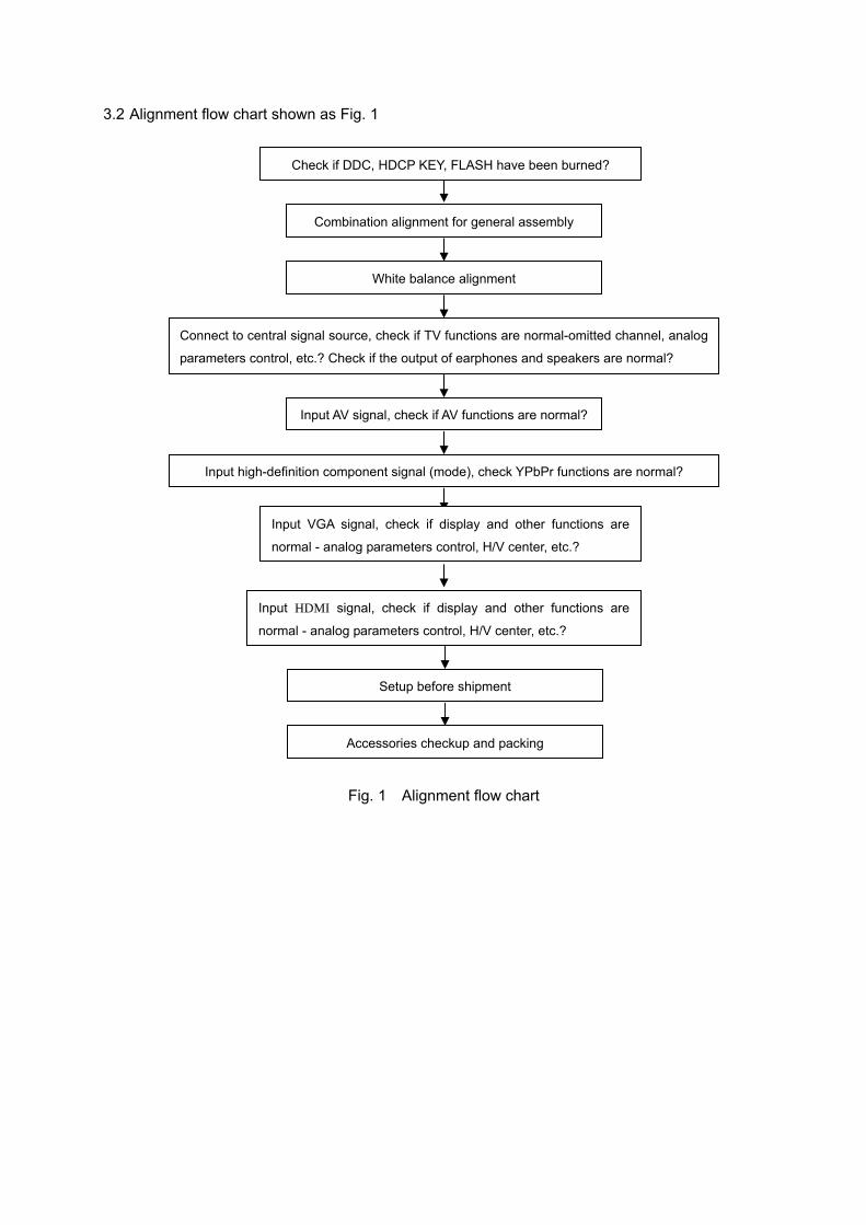
3.2 Alignment flow chart shown as Fig. 1
Fig. 1 Alignment flow chart
Check if DDC, HDCP KEY, FLASH have been burned?
Combination alignment for general assembly
White balance alignment
Connect to central signal source, check if TV functions are normal-omitted channel, analog
parameters control, etc.? Check if the output of earphones and speakers are normal?
Input high-definition component signal (mode), check YPbPr functions are normal?
Input VGA signal, check if display and other functions are
normal - analog parameters control, H/V center, etc.?
Input AV signal, check if AV functions are normal?
Setup before shipment
Accessories checkup and packing
Input HDMI signal, check if display and other functions are
normal - analog parameters control, H/V center, etc.?
4 Alignment instructions
4.1 Unit adjustment 4.1.1 According to the wiring of “9232KH4601JL”, connect main board, power board and IR board correctly, then switch on the main power and press key “standby” to turn on the TV set. Check if display is normal? 4.1.2 Using method of factory menu
a) Press key “SOURCE” first, then press keys “2, 5, 8, 0” in turn to enter into initial factory menu;
b) Press keys “” and “” to move cursor to each page of initial factory menu, then press “OK” to enter into adjusting menu of each page;
c) Press keys “” and “” to move cursor upwards or downwards within any page; d) Press keys “” and “” to do adjustment when cursor is moved to any item; e) Press key “MENU” to exit menu of any page to its superior factory menu; f) Press key “EXIT” to exit factory menu in any case; g) Press key “OK” to enter into inferior factory menu; h) Factory menu item: ADC ADJUST, for ADC calibration of VGA and Component; i) Factory menu item: W/B ADJUST, for white balance adjustment; j) Factory menu item: POWER Mode, for setting power-on mode; the default setting is
“Standby” mode unless specified by customer; Standby: TV set will be in “standby” mode after power-on; MEM: TV set will keep states before last power-off; ForceOn: TV set will turn on automatically; it also can be used as aging mode at factory;
k) Factory menu item: Other Setting->ISP Mode, the item will not be kept in memory, that is, it will be always in “OFF” mode after turning on again; “ON”: Upgrading unit software through VGA port while connecting to ISP device; “OFF”: Normal DDC functions of VGA port will recover;
l) Factory menu item: EEPROM Init, for factory and customer data initialization; TV set will reset and initial guiding interface will display after executing the item;
m) Factory menu item: Factory ChA., for factory channels presetting; it is necessary to connect to central signal source before operating the item; now digital frequency of central signal CH28(529.5 MHz)and CH33(564.5 MHz)are distributed to Australia programs; originally preset digital programs will not change along with the modification of central signal, so please operate item “DTV” of menu “Channel” to search digital programs manually, which will last about 15s;
n) Factory menu item: Shipment, all DTV/ATV programs for factory adjustment will be cleared out first, then ATV channels will be preset according to customer requirements; the item must be executed before shipment to clear out channels for factory adjustment;
o) Factory menu item: Other Setting->MST DEBUG, default setting is “OFF”, it will not be kept in memory, that is, it will always in “OFF” mode after turning on the set again; “OFF”: RS232 functions of some engineering machines can match design specifications; “ON”: It is convenient for design tools to debug the software;
p) Factory menu item: Backlight, for adjusting brightness of backlight; test voltage of X108-12# (PWM) while adjusting the item to meet the requirements of PWM voltage scope corresponding to mixture brightness described by panel specification; the item need not adjustment for it has been preset by software;
q) Factory menu item: Other Setting->SSC ADJUST, for expanded spectrum adjustment; the item need not adjustment for it has been preset by software;
r) Factory menu item: Other Setting->AUDIO Curve Setting, for sound curve adjustment; if without special customer requirements, the item need not adjustment commonly for it has been preset by software;
Note: If software is upgraded or there have been date in EEPROM already, please execute item “RESET ALL” to clear out all data before adjustment for the first time. 4.2 ADC calibration 4.2.1 ADC calibration of VGA
1) Switch “source” to VGA channel; 2) Press key “SOURCE”, then press keys “2, 5, 8, 0” in turn to enter into initial factory menu; 3) Move cursor to item “ADC ADJUST” and press key “OK” to enter into inferior factory menu; 4) Input VGA signal(VG848: Timing 856(1024×768/60 Hz), Pattern 920 Gray 8 step(H));
move cursor to item “MODE ”,press keys “” and “” to select item “RGB”,then move cursor to item “AUTO ADC” and press key “OK” to begin auto-adjustment until completing the calibration.
4.2.2 ADC calibration of YPbPr 1) Switch “source” to YPbPr channel; 2) Press key “SOURCE”, then press keys “2, 5, 8, 0” in turn to enter into initial factory menu; 3) Move cursor to item “ADC ADJUST” and press key “OK” to enter into inferior factory menu; 4) Input Y/Pb/Pr signal(VG848 Timing 976(720P),Pattern 918 SMPTE Color Bar); move
cursor to item “MODE ”,press keys “” and “” to select item “YPbPr”,then move cursor to item “AUTO ADC” and press key “ENTER” to begin auto-adjustment until completing the calibration, prompt “SUCCESS” displaying below “AUTO ADC” means successful auto-calibration.
4.3 White balance adjustment
Unless specified by customer, default color temperature “COOL” is 12000K and its chromatic coordinates is (272, 278); color temperature “NORMAL” is 9300K and its chromatic coordinates is
(285, 293); color temperature “WARM” is 6500K and its chromatic coordinates is (323、329); 4.3.1 Adjustment procedure
TV set should be working over 30 mins to be in stabler state before white balance adjustment; Use white balance apparatus CA210 and switch to its BBY channel.
1) Switch “source” to HDMI channel; 2) Press key “SOURCE”, then press keys “2, 5, 8, 0” in turn to enter into initial factory menu; 3) Move cursor to item “W/B ADJUST” and press key “OK” to enter into inferior factory menu; 4) Input DVI/HDMI signal (16 Gray Scale Signal: 1024×768/60Hz, TIMING: 856,
PATTERN:921); move cursor to item “MODE”, press keys “” and “” to select item “HDMI1” or other HDMI channels, then move cursor to item “TEMPERATURE” and press keys “” and “” to select item “COOL”;
5) Adjust items “R-GAIN, G-GAIN, B-GAIN” to set chromatic coordinates of 14th scale as (272, 278);
6) Adjust items “R-OFFSET, G-OFFSET, B-OFFSET” to set chromatic coordinates of 4th scale as (272, 278);
7) During adjustment, make sure that chromatic coordinates of bright scale are (X=272±10, Y=278±10) and chromatic coordinates of dark scale are (X=272±10, Y=278±10);
8) Move cursor to item “COPY ALL” again to copy data of white balance to other channels except DTV;
9) Check if chromatic coordinates of HDMI NORMAL and WARM meet the requirements of error allowance (dark scale: ±10, bright scale: ±10) or not, otherwise adjust items “R_GAIN/B_GAIN/R_OFF/B_OFF” to meet them and then save the data;
10) Switch to other channels (ATV, AV,COMPONENT,D-SUB), check if chromatic coordinates of COOL, NORMAL and WARM meet the requirements or not, if not, adjust them respectively in the same way of HDMI and with 16 gray scale signal; exit menu “W/B ADJUST” after adjustment, the data will be save automatically;
11) DTV adjustment: switch to DTV channel, select 16 gray scale program, enter into factory menu, do adjustment following above step 5, 6, 7;
12) Please refer to the adjusting rules as follows: B Gun: coordinates of X and Y will increase when B gun is adjusted downwards;
coordinates of X and Y will decrease when B gun is adjusted upwards; R Gun: adjusting R gun will effect coordinate of X, and value of Lv slightly; coordinate of X will increase when R gun is adjusted upwards;
coordinate of X will decrease when R gun is adjusted downwards; G Gun: adjusting G gun will effect coordinate of Y, and value of Lv greatly; coordinate of Y will increase when G gun is adjusted upwards;
coordinate of Y will decrease when G gun is adjusted downwards; Note: Default color temperature specified by SANYO customer is Normal, adjust chromatic coordinates of Normal and Cool in Dynamic picture mode; adjust chromatic coordinates of Cool in Dynamic picture mode for other customers.
5 Functions checkup
5.1 TV functions Input central signal to RF port, enter into menu “CHANNEL” first, then search channels
automatically, check if there is any omitted channel, check if the output of speakers and the picture are normal. 5.2 AV port
Input signal to AV port respectively, check if the picture and the sound are normal. 5.3 YPbPr/YCbCr port
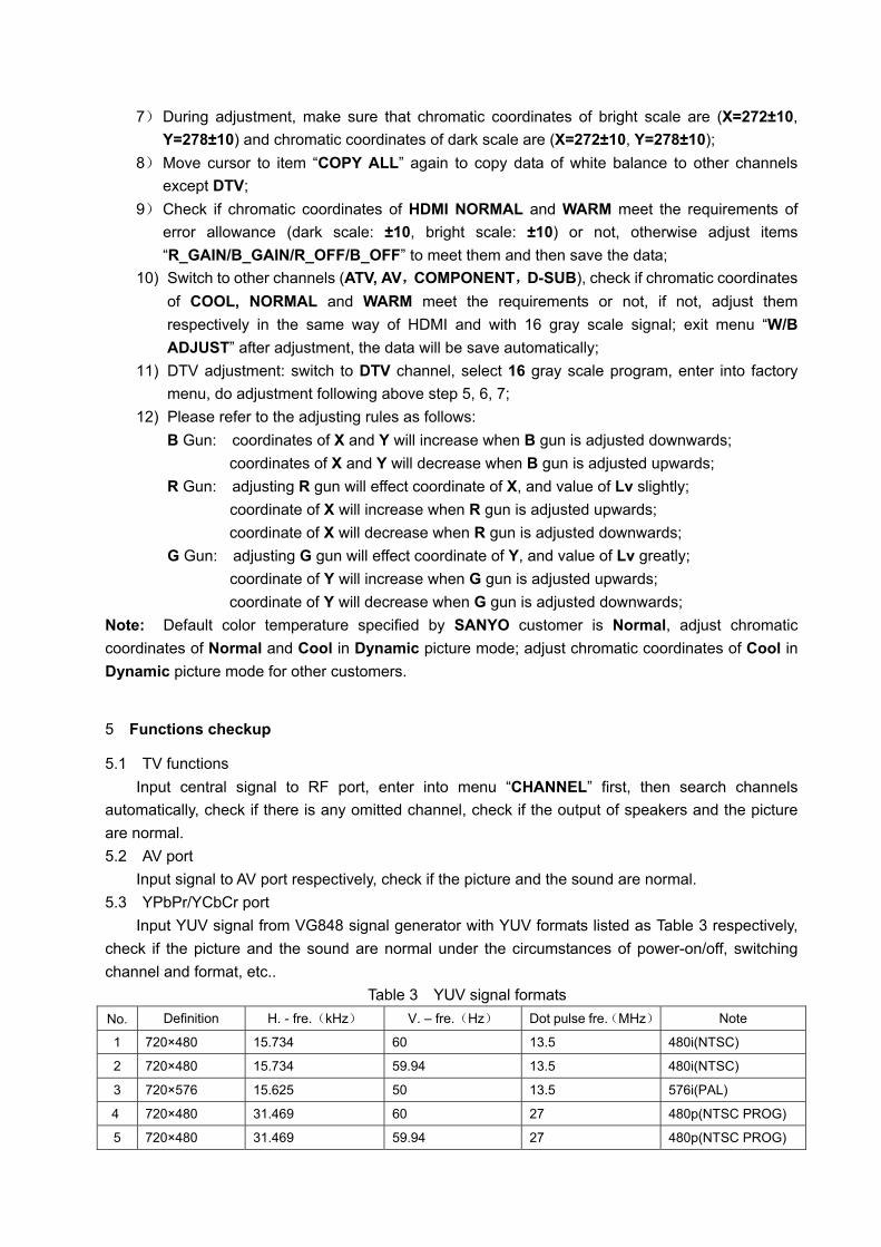
Input YUV signal from VG848 signal generator with YUV formats listed as Table 3 respectively, check if the picture and the sound are normal under the circumstances of power-on/off, switching channel and format, etc..
Table 3 YUV signal formats No. Definition H. - fre.(kHz) V. – fre.(Hz) Dot pulse fre.(MHz) Note
1 720×480 15.734 60 13.5 480i(NTSC)
2 720×480 15.734 59.94 13.5 480i(NTSC)
3 720×576 15.625 50 13.5 576i(PAL)
4 720×480 31.469 60 27 480p(NTSC PROG)
5 720×480 31.469 59.94 27 480p(NTSC PROG)
No. Definition H. - fre.(kHz) V. – fre.(Hz) Dot pulse fre.(MHz) Note
6 720×576 31.25 50 27 576p(PAL PROG)
7 1280×720 45 59.94 74.18 720p(59p)
8 1280×720 45 60 74.25 720p(60p)
9 1280×720 37.5 50 74.25 720p(50p)
10 1920×1080 33.75 59.94 74.25 1080i(59i)
11 1920×1080 33.75 60 74.25 1080i(60i)
12 1920×1080 28.125 50 74.25 1080i(50i)
13 1920×1080 67.5 59.94 148.35 1080p(59p)
14 1920×1080 67.5 60 148.5 1080p(60p)
15 1920×1080 56.25 50 148.5 1080p(50p)
16 1920×1080 - 23.94/24 - -
17 1920×1080 - 25 - -
18 1920×1080 - 29.97/30 - -
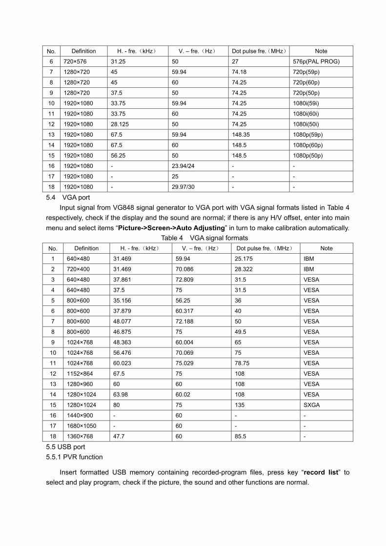
5.4 VGA port Input signal from VG848 signal generator to VGA port with VGA signal formats listed in Table 4
respectively, check if the display and the sound are normal; if there is any H/V offset, enter into main menu and select items “Picture->Screen->Auto Adjusting” in turn to make calibration automatically.
Table 4 VGA signal formats No. Definition H. - fre.(kHz) V. – fre.(Hz) Dot pulse fre.(MHz) Note
1 640×480 31.469 59.94 25.175 IBM
2 720×400 31.469 70.086 28.322 IBM
3 640×480 37.861 72.809 31.5 VESA
4 640×480 37.5 75 31.5 VESA
5 800×600 35.156 56.25 36 VESA
6 800×600 37.879 60.317 40 VESA
7 800×600 48.077 72.188 50 VESA
8 800×600 46.875 75 49.5 VESA
9 1024×768 48.363 60.004 65 VESA
10 1024×768 56.476 70.069 75 VESA
11 1024×768 60.023 75.029 78.75 VESA
12 1152×864 67.5 75 108 VESA
13 1280×960 60 60 108 VESA
14 1280×1024 63.98 60.02 108 VESA
15 1280×1024 80 75 135 SXGA
16 1440×900 - 60 - -
17 1680×1050 - 60 - -
18 1360×768 47.7 60 85.5 -
5.5 USB port 5.5.1 PVR function
Insert formatted USB memory containing recorded-program files, press key “record list” to select and play program, check if the picture, the sound and other functions are normal.
5.5.2 Media playing function: Insert USB memory containing files of picture, audio and video, check if the picture, the sound
and other functions are normal. 5.6 MUSIC port (only for SANYO model)
Input audio signal from sound output device to side music port, check if the sound is normal.
5.7 HDMI port Input HDMI signal from VG849 signal generator to HDMI port with the formats listed in Table 3
and Table 4 respectively, check if the display and the sound (32 kHz, 44.1 kHz, 48 kHz) are normal under the circumstances of power-on, switching channels or formats, etc 5.8 Other functions checkup
Check if functions - timing on/off, sleeping off, picture/sound mode, OSD, stereo and digital audio ports, etc., are normal;
Check if pure audio program (RADIO) are normal when switching to digital programs;
Check if functions of LCN and OTA are normal.
6 User menu setup before shipment
Enter into page “LOCK” of user menu, select item “Restore Factory Default” to make setup before shipment.
Main procedures as follows:
1)Clear out information of all programs;
2)Clear out information about VCHIP – parents control;
3)Default analog parameters setup for user;
4)Set Menu Language as “English”;
5)Set Power on mode as “Off”.
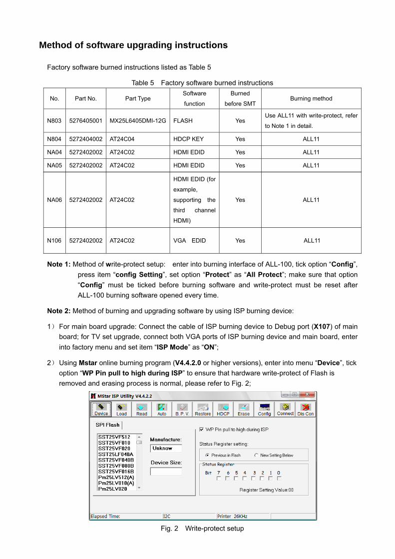
NA06 5272402002 AT24C02
HDMI EDID (for
example,
supporting the
third channel
HDMI)
Yes ALL11
N106 5272402002 AT24C02 VGA EDID Yes ALL11
Note 1: Method of write-protect setup: enter into burning interface of ALL-100, tick option “Config”, press item “config Setting”, set option “Protect” as “All Protect”; make sure that option “Config” must be ticked before burning software and write-protect must be reset after ALL-100 burning software opened every time.
Note 2: Method of burning and upgrading software by using ISP burning device:
1) For main board upgrade: Connect the cable of ISP burning device to Debug port (X107) of main board; for TV set upgrade, connect both VGA ports of ISP burning device and main board, enter into factory menu and set item “ISP Mode” as “ON”;
2) Using Mstar online burning program (V4.4.2.0 or higher versions), enter into menu “Device”, tick option “WP Pin pull to high during ISP” to ensure that hardware write-protect of Flash is removed and erasing process is normal, please refer to Fig. 2;
Fig. 2 Write-protect setup
Factory software burned instructions listed as Table 5
Table 5 Factory software burned instructions
No. Part No. Part Type Software
function
Burned
before SMTBurning method
N803 5276405001 MX25L6405DMI-12G FLASH Yes Use ALL11 with write-protect, refer
to Note 1 in detail.
N804 5272404002 AT24C04 HDCP KEY Yes ALL11
NA04 5272402002 AT24C02 HDMI EDID Yes ALL11
NA05 5272402002 AT24C02 HDMI EDID Yes ALL11
Method of software upgrading instructions
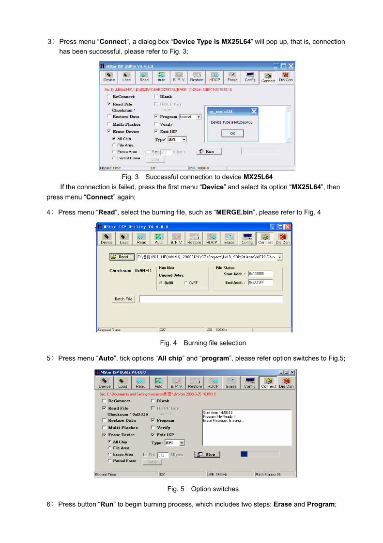
Fig. 3 Successful connection to device MX25L64
If the connection is failed, press the first menu “Device” and select its option “MX25L64”, then press menu “Connect” again;
4) Press menu “Read”, select the burning file, such as “MERGE.bin”, please refer to Fig. 4
Fig. 4 Burning file selection
5) Press menu “Auto”, tick options “All chip” and “program”, please refer option switches to Fig.5;
Fig. 5 Option switches
6) Press button “Run” to begin burning process, which includes two steps: Erase and Program;
3) Press menu “Connect”, a dialog box “Device Type is MX25L64” will pop up, that is, connection has been successful, please refer to Fig. 3;
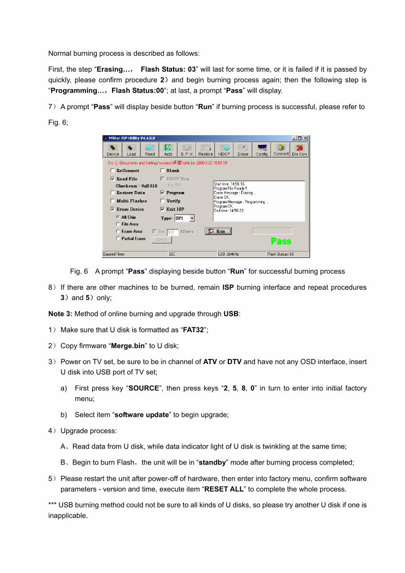
Normal burning process is described as follows:
First, the step “Erasing…, Flash Status: 03” will last for some time, or it is failed if it is passed by quickly, please confirm procedure 2)and begin burning process again; then the following step is “Programming…,Flash Status:00”; at last, a prompt “Pass” will display.
7) A prompt “Pass” will display beside button “Run” if burning process is successful, please refer to
Fig. 6;
Fig. 6 A prompt “Pass” displaying beside button “Run” for successful burning process
8) If there are other machines to be burned, remain ISP burning interface and repeat procedures 3)and 5)only;
Note 3: Method of online burning and upgrade through USB:
1) Make sure that U disk is formatted as “FAT32”;
2) Copy firmware “Merge.bin” to U disk;
3) Power on TV set, be sure to be in channel of ATV or DTV and have not any OSD interface, insert U disk into USB port of TV set;
a) First press key “SOURCE”, then press keys “2, 5, 8, 0” in turn to enter into initial factory menu;
b) Select item “software update” to begin upgrade;
4) Upgrade process:
A、Read data from U disk, while data indicator light of U disk is twinkling at the same time;
B、Begin to burn Flash,the unit will be in “standby” mode after burning process completed;
5) Please restart the unit after power-off of hardware, then enter into factory menu, confirm software parameters - version and time, execute item “RESET ALL” to complete the whole process.
*** USB burning method could not be sure to all kinds of U disks, so please try another U disk if one is inapplicable.
Working principle analysis of the unit Signal Flow
1、 PAL signal flow
Send PAL analog RF signal received from antenna to TUNER FT2119 which is controlled by main chip MSD209GL through I2C BUS; after frequency conversion by Tuner, analog IF output signal is pre-amplified and then filtered by both picture and sound SAW, then it is sent out to demodulator IC MSB1210; CVBS video signal and SIF audio differential signal will be outputted after demodulation; CVBS video signal is sent into main chip MSD209GL to be processed by modules of video decoding, deinterlacing, video processing and zoom, then LVDS signal will be outputted to drive display panel; SIF audio differential signal is sent into main chip MSD209GL to be demodulated to analog audio signal, then it is sent to earphone amplifier BH3547F to be amplified after the processes of preamplification, acoustic effect processing and volume control, and then it is divided into two, one is sent to earphone jack, the other is sent to digital audio power amplifier R2A15112 to be amplified and then drive speakers.
2、 DVB-T signal flow Send DVB-T digital RF signal received from antenna to TUNER FT2119 which is controlled by main chip MSD209GL through I2C BUS; after down frequency conversion, differential IF signal will be inputted to demodulator IC MSB1210 to be demodulated; then it will be sent to main chip MSD209GL with the standard format of serial TS stream for demultiplexing and decoding; Video route: digital video signal is sent into main chip MSD209GL for decoding and video processing after demultiplexing, then LVDS signal will be outputted to drive display panel; Audio route: digital audio signal will be sent into main chip MSD209GL for decoding and audio processing after demultiplexing, then dual-sound-track analog audio signal (stereo) is sent to earphone amplifier BH3547F to be amplified after the processes of preamplification, acoustic effect processing and volume control by main chip MSD209GL, then one is sent to earphone jack, the other is sent to digital audio power amplifier R2A15112 to be amplified and then drive speakers.
3、 AV input signal flow AV video signal is sent into main chip MSD209GL to be processed by modules of video decoding, deinterlacing, video processing and zoom, then LVDS signal will be outputted to drive display panel; AV audio signal is sent into main chip MSD209GL for acoustic effect processing and volume control after the processing of voltage division, impendence matching and AC coupling, then it is sent to earphone amplifier BH3547F to be amplified, one is sent to earphone jack, the other is sent to digital audio power amplifier R2A15112 to be amplified and then drive speakers.
4、 D-SUB/YPbPr input signal flow D-SUB/YPbPr video signal is sent into main chip MSD209GL to be processed by modules of A/D conversion, video decoding, deinterlacing, video processing and zoom, then LVDS signal will be outputted to drive display panel; D-SUB/YPbPr audio signal is sent into main chip MSD209GL for acoustic effect processing and volume control after the processing of voltage division, impendence matching and AC coupling, then it is sent to earphone amplifier BH3547F to be amplified, one is sent to earphone jack, the other is sent to digital audio power amplifier R2A15112 to be amplified and then drive speakers.
5、 HDMI input signal flow HDMI video signal is sent into main chip MSD209GL to be processed by modules of video decoding, video processing and zoom, then LVDS signal will be outputted to drive display panel; HDMI audio signal is sent into main chip MSD209GL for audio processing, preamplification, acoustic effect processing and volume control, then it is sent to earphone amplifier BH3547F to be amplified, one is sent to earphone jack, the other is sent to digital audio power amplifier R2A15112 to be amplified and then drive speakers.
6、 AV input signal flow Current active AV video signal is sent into main chip MSD209GL for video coding, then it is amplified
by peripheral video amplified circuits and then outputted; Current active AV audio signal is sent into main chip MSD209GL for preamplification, acoustic effect
processing and volume control, then it is sent to operation amplifier to be amplified and then outputted.
Brief Instruction of the Unit MPEG-2 MP@HL、H.264 Main and High profile up to Leve4.0 Decoding MPEG、Dolby Digital(AC-3)、Digital audio decoding (AAC) 3D comb filter Wide range power supply, low power consumption in standby mode(≤1W) Audio power amplifier (class D), HI-quality acoustic effect output Hi-quality processing of interlaced to progressive scanning Real integrative functions realization:
- Integrative structure - Integrative Tuner (A/D integration) - Channel-searching integration - OSD interface integration Main components of the unit:
32” LCD panel(1920X1080) Main chip:MStar MSD209GL-LF Demodulator chip:MStar MSB1210-LF Tuner:NXP FT2119 DDR:SAMSUNG K4T1G164QE-HCF7 Power amplifier (class D):RENESAS R2A15112
FLASH :MX25L6405DMI-12G External interfaces of the unit:
Two groups of Video and one group of RCA L/R input Three groups of HDMI input One group of VGA input One group of audio input For VGA and DVI(Mini Phone Jack) Two groups of YPBPR以及 RCA L/R input One group of RF One group of RS232(Mini Phone Jack) One group of audio output(Mini Phone Jack)

One group of Video and RCA L/R output One group of SPDIF(coaxial)output One group of USB for upgrading
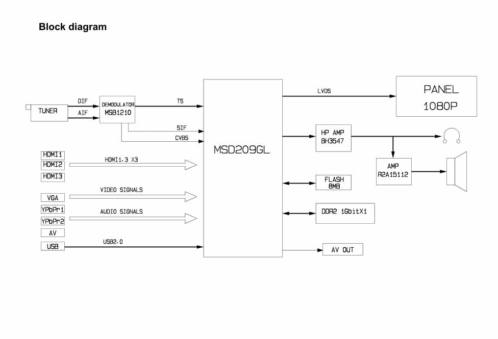
Block diagram
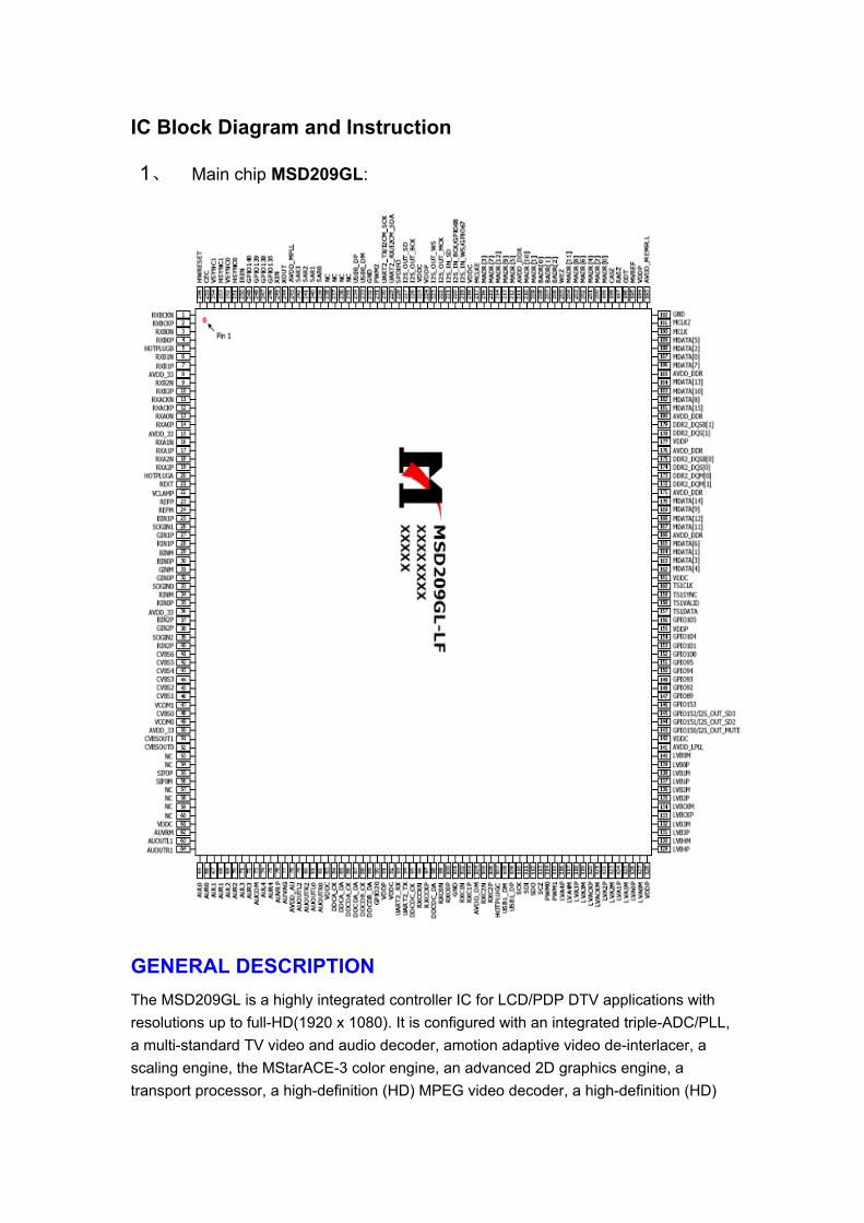
IC Block Diagram and Instruction
1、 Main chip MSD209GL:
GENERAL DESCRIPTION
The MSD209GL is a highly integrated controller IC for LCD/PDP DTV applications with resolutions up to full-HD(1920 x 1080). It is configured with an integrated triple-ADC/PLL, a multi-standard TV video and audio decoder, amotion adaptive video de-interlacer, a scaling engine, the MStarACE-3 color engine, an advanced 2D graphics engine, a transport processor, a high-definition (HD) MPEG video decoder, a high-definition (HD)
H.264 video decoder, a RealVideo decoder, a JPEG video decoder, a MPEG-4 decoder, and a 24-bit DSP for MPEG audio decoding, a DVI/HDCP/HDMI receiver, and a peripheral control unit providing a variety of HDTV control functions. For digital TV application, the MSD209GL comprises an MPEG-2 transport processor with advanced section filtering capability, an MPEG-2 (MP@HL profile) video decoder, a MPEG-4 decoder, a H.264 video decoder, and an audio DSP decoder for MPEG audio streams, MPEG layer I and II digital audio decoder with analog audio outputs that are designed to support existing and future DVB-T programs while handling conditional access. Furthermore,it is also possible to decode JPEG, RealVideo streams, and MP3 formats from external sources such as USB interface. For analog TV, the MSD209GL includes NTSC/PAL/SECAM multi-standard video decoder comprising a 3D motion adaptive comb filter and time-based correction, and a NICAM/A2 audio decoder to support worldwide television standards. The MSD209GL is also configured with a VBI processor to decode digital information such as Close Caption/V-chip/teletext/WSS/CGMS-A/VPS. In addition, the MStar advanced LCD TV processor enhances video quality, motion adaptive de-interlacer, picture quality adjustment units, and MStarACE-3 color engine. With USB 2.0 host controllers, UART, IR, SPI, I2C, and PWM, the MSD209GL fulfills all requirements in advanced DTV sets. To reduce system costs, the MSD209GL also integrates intelligent power management control capability for green-mode requirements and spread-spectrum support for EMI management.
MSD209GL Features: Twin -turbo 8051 Micro-controller
· Twin-turbo 8051 MCU · Interrupt controller · Supports ISP · Two full duplex UARTs · DMA engine to speed up large data movement Transport St ream De-multiplexer
· Supports serial TS interface, with or without sync signal · Maximum TS data rate is 104 Mb/sec · 32 general purpose PID filters and section filters for each transport stream de-multiplexer · One video PES and one audio PES channel · Supports DVB subtitle and digital teletext · Supports additional audio/video/PCR filters · Supports TS DMA channel for time-shift MPEG -2 A/V Decoder
· ISO/IEC 13818-2 MPEG-2 video MP@HL · Supports resolution in HDTV (1080i, 720p) and SDTV
· Supports MPEG-1, MPEG-2 (Layer I/II), Dolby Digital (AC-3), and AAC audio decoding
MPEG -4 Video Decoder · ISO/IEC 14496-2 MPEG-4 ASP video decoding · Supports resolution in HDTV (1080p@30fps) H.264 Decoder
· ITU-T H.264, ISO/IEC 14496-10 (main and high profile up to level 4.0) video decoding · Supports resolutions for all DVB, ATSC, HDTV, DVD and VCD · Supports resolution up to 1080p@30fps · Supports CABAC and CAVLC stream types · Processing of ES and PES streams, extractions and provision of time stamps RealMedia Decoder
· Supports maximum resolution up to 720p@30fps · Supports RV8, RV9, RV10, RA8-LBR and HE-AAC decoders · Supports file formats with RM and RMVB · Supports Picture Re-sampling · Supports in-loop de-block for B-frame Hardware JPEG
· Supports sequential mode, single scan · Supports both color and grayscale picture · Operates in scan unit; hardware decoder will handle the bit stream after scan header · Supports programmable region of interest (ROI) · Supports scaling down ratio: 1/2, 1/4, 1/8, applied to height and width simultaneously
NTSC/PAL/SECAM Video Decoder · Supports NTSC-M, NTSC-J, NTSC-4.43, PAL (B, D, G, H, M, N, I, Nc), and SECAM · Automatic TV standard detection · Motion adaptive 3D comb filter for NTSC/PAL · Supports Teletext level-1.5, Closed Caption (analog CC 608/ analog CC 708/digital CC 608/digital CC 708), V-chip and SCTE · Two CVBS video outputs
Multi -Standard TV Sound Processor · Supports BTSC/A2/EIA-J demodulation in NTSC and A2/NICAM/FM/AM demodulation in PAL · Supports MTS Mode Mono/Stereo/SAP in BTSC/EIA-J and Mono/Stereo/Dual in A2/NICAM
· Built-in audio DAC’s · Audio processing for loudspeaker channel, including volume, balance, mute, tone, EQ, virtual stereo/surround, and treble/bass · Supports digital audio format decoding: MPEG-1, MPEG-2 (Layer I/II), MP3, AC-3 (Dolby Digital), AAC-LC, WMA
Digital Audio Interface · I2S digital audio input & output · S/PDIF digital audio input & output · HDMI audio channel processing capability · Programmable delay for audio/video synchronization Analog RGB Compliant In put Ports
· Three analog ports support up to 1080P · Supports PC RGB input up to SXGA@75Hz · Supports HDTV RGB/YPbPr/YCbCr · Supports Composite Sync and SOG (Sync-on-Green) separator · Automatic color calibration DVI/HDCP/HDMI Compliant Input Port
· Three DVI/HDCP/HDMI input ports support up to 225MHz @ 1080P 60Hz with 12-bit deep-color resolution · Single link on-chip DVI 1.0 compliant receiver · High-bandwidth Digital Content Protection (HDCP) 1.1 compliant receiver · High Definition Multimedia Interface (HDMI) 1.3 compliant receiver with CEC (Consumer Electronics Control) support · Long-cable tolerant robust receiving MACE -4, MStar Advanced Color Engine year 2009 Edition, provides superb visual
quality for wider gamut FHD panels · Fully programmable shrink/zoom capabilities · Panorama and various scaling supports · 3D motion adaptive video de-interlacers with de-flickering and edge smoothing functions · Automatic 3:2 pull-down & 2:2 pull-down detection and recovery
· Supports sRGB and xvYCC color processing · Supports HDMI 1.3 deep color format · Supports linear/nonlinear color mapping for wider gamut panels · 10-bit internal data processing · Programmable 12-bit RGB gamma CLUT · 3D video noise reduction · MPEG artifact removal including de-blocking and mosquito noise reduction · Frame rate conversion Output Interface
· Supports up to 10-bit dual LVDS full-HD (1920 x 1080) panel interface · Supports 2 data output formats: Thine & TI data mappings · Spread spectrum output frequency for EMI suppression
CVBS Video Output 2D Graphics Engine
· 256-pin LQFP package · Operating at 1.26V (core), 1.8V (DDR2), and 3.3V (I/O and analog)
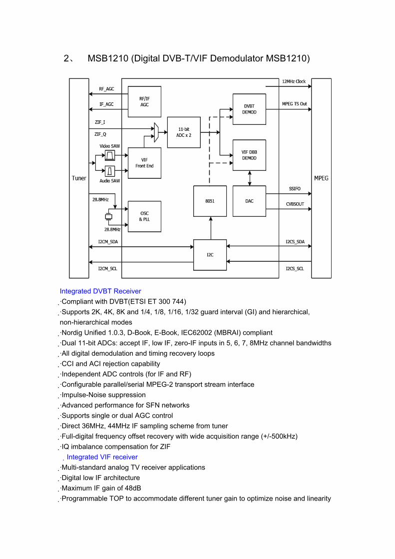
2、 MSB1210 (Digital DVB-T/VIF Demodulator MSB1210)
Integrated DVBT Receiver · Compliant with DVBT(ETSI ET 300 744) · Supports 2K, 4K, 8K and 1/4, 1/8, 1/16, 1/32 guard interval (GI) and hierarchical, non-hierarchical modes · Nordig Unified 1.0.3, D-Book, E-Book, IEC62002 (MBRAI) compliant · Dual 11-bit ADCs: accept IF, low IF, zero-IF inputs in 5, 6, 7, 8MHz channel bandwidths · All digital demodulation and timing recovery loops · CCI and ACI rejection capability · Independent ADC controls (for IF and RF) · Configurable parallel/serial MPEG-2 transport stream interface · Impulse-Noise suppression · Advanced performance for SFN networks · Supports single or dual AGC control · Direct 36MHz, 44MHz IF sampling scheme from tuner · Full-digital frequency offset recovery with wide acquisition range (+/-500kHz) · IQ imbalance compensation for ZIF Integrated VIF receiver
· Multi-standard analog TV receiver applications · Digital low IF architecture · Maximum IF gain of 48dB · Programmable TOP to accommodate different tuner gain to optimize noise and linearity
performance Miscellaneous
· Embedded 8-bit MCU · Clock generation from a single 24MHz crystal · Supports I2C interface with bypass mode · Operating voltage: 3.3V and 1.2V · 48-pin LQFP package
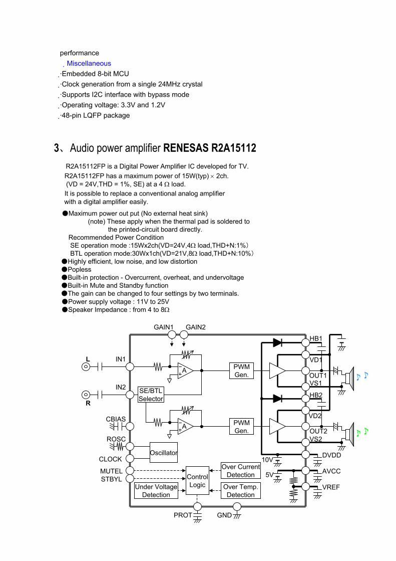
3、 Audio power amplifier RENESAS R2A15112 R2A15112FP is a Digital Power Amplifier IC developed for TV. R2A15112FP has a maximum power of 15W(typ) × 2ch.
(VD = 24V,THD = 1%, SE) at a 4 Ω load. It is possible to replace a conventional analog amplifier
with a digital amplifier easily.
Maximum power out put (No external heat sink) (note) These apply when the thermal pad is soldered to
the printed-circuit board directly. Recommended Power Condition SE operation mode :15Wx2ch(VD=24V,4Ω load,THD+N:1%) BTL operation mode:30Wx1ch(VD=21V,8Ω load,THD+N:10%)
Highly efficient, low noise, and low distortion PoplessBuilt-in protection - Overcurrent, overheat, and undervoltageBuilt-in Mute and Standby functionThe gain can be changed to four settings by two terminals.
Power supply voltage : 11V to 25V Speaker Impedance : from 4 to 8Ω
Under VoltageDetection
Over Temp.Detection
Over CurrentDetectionControl
LogicSTBYL
GND
IN1
A
MUTEL
PROT
CBIASA
IN2
PWMGen.
PWMGen.
Oscillator
ROSC
GAIN1 GAIN2
SE/BTLSelector
OUT1
HB1
VD1
VS1
OUT2
VD2
VS2
HB2
DVDD
AVCC
R
L
CLOCK
VREF
10V
5V
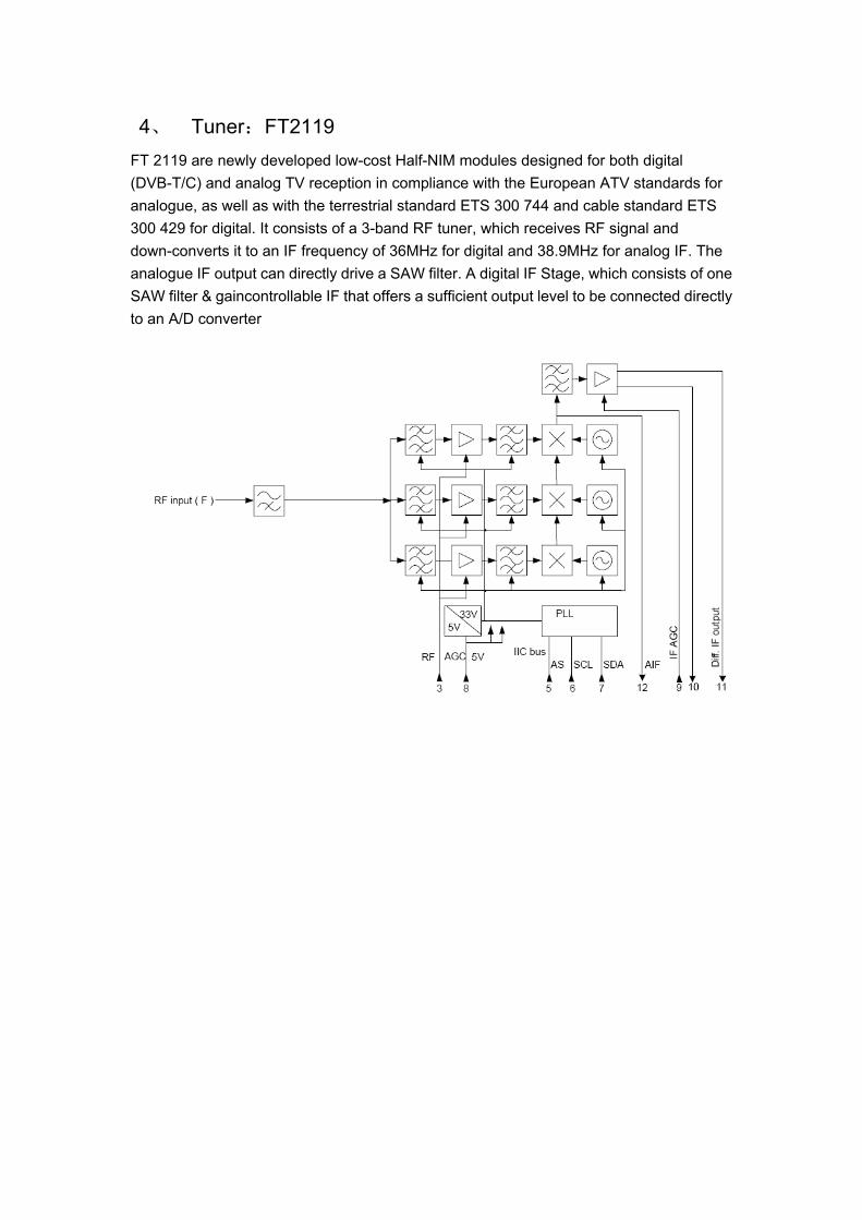
4、 Tuner:FT2119 FT 2119 are newly developed low-cost Half-NIM modules designed for both digital (DVB-T/C) and analog TV reception in compliance with the European ATV standards for analogue, as well as with the terrestrial standard ETS 300 744 and cable standard ETS 300 429 for digital. It consists of a 3-band RF tuner, which receives RF signal and down-converts it to an IF frequency of 36MHz for digital and 38.9MHz for analog IF. The analogue IF output can directly drive a SAW filter. A digital IF Stage, which consists of one SAW filter & gaincontrollable IF that offers a sufficient output level to be connected directly to an A/D converter
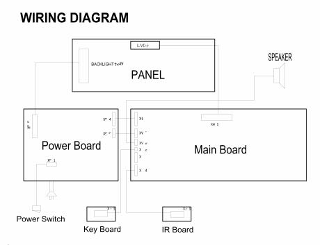
WIRING DIAGRAM
PANEL
Main Board
P
Power Board
BACKLIGHT
SPEAKER
IR BoardKey BoardPower Switch
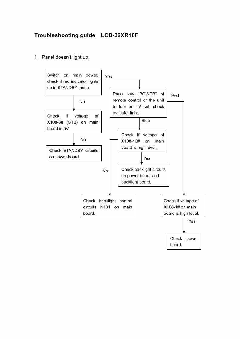
Troubleshooting guide LCD-32XR10F
1.Panel doesn’t light up.
Yes Red No Blue
No Yes No
Switch on main power, check if red indicator lights up in STANDBY mode.
Check backlight circuits on power board and backlight board.
Press key “POWER” of remote control or the unit to turn on TV set, check indicator light.
Check if voltage of X108-13# on main board is high level.
Check if voltage of X108-3# (STB) on main board is 5V.
Check STANDBY circuits on power board.
Yes
Check backlight control circuits N101 on main board.
Check if voltage of X108-1# on main board is high level.
Check power board.
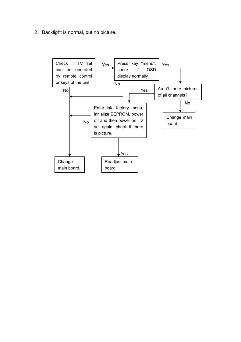
2.Backlight is normal, but no picture.
Yes Yes No No Yes TV No 有 No
Yes
Check if TV set can be operated by remote control or keys of the unit.
Aren’t there pictures of all channels?
Change main board.
Enter into factory menu, initialize EEPROM, power off and then power on TV set again, check if there is picture.
Press key “menu”, check if OSD display normally.
Change main board.
Readjust main board.
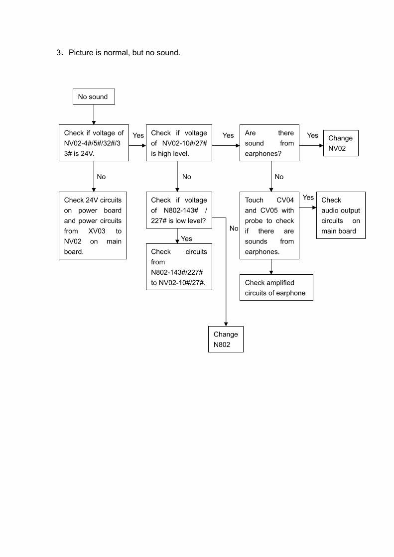
3.Picture is normal, but no sound.
No sound
Yes Yes Yes No No No Yes
No
Yes
Check if voltage of NV02-4#/5#/32#/33# is 24V.
Check 24V circuits on power board and power circuits from XV03 to NV02 on main board.
Check if voltage of NV02-10#/27# is high level.
Check if voltage of N802-143# / 227# is low level?
Are there sound from earphones?
ChangeNV02
Check amplified circuits of earphone
Touch CV04 and CV05 with probe to check if there are sounds from earphones.
Check audio output circuits on main board
Check circuits from N802-143#/227# to NV02-10#/27#.
Change N802
XOCECOSheet to
DRAWN BY71
X1.3
TUNER+DEMODULATOR
9232KH4601DL
XIAMEN OVERSEAS CHINESE ELECTRONIC CO., LTD.
TITLE: DWG NO.
REV.
APPROVED BY
TUNER1
DT70GI-2-E
TS_MDI[0]TS_MIVALTS_MISTRTTS_MICLK
TUNER_SCL
TS_MISTRT
TUNER_SDA
TS_MICLK
RST_1210
GND-D
+3.3V_DE
GND-D
TS_MIVAL
TV_IF_AGC
TS_MDI[0]
GND-D
+3.3V_DE
GND-D
TUNER_SDA
SDA 007:A4
+5V_TUNER
Z101K9656
1 2 3 4 5
T_RF_AGC
C11410n
V102BC847AW
TUNER_SCL
TV_FAT_IFP
SCL 007:A4
TV_IF_AGC
Z102K3953
1 2 3 4 5
TV_FAT_IFN
L104
0.56uH
+12V
GND-D
GND-D
GND-D
GND-D
GND-D
VIFM
VIFP
TV_SIFM
TV_SIFP
VIFMVIFP
TV_SIFPTV_SIFM
GND-D
GND-D
GND-D
SIFM
SIFP
TV_INM
TV_INP
VJ01
MMBT3906LT1
VJ02MMBT3904
T_RF_AGC
GND-D
VDDC +1.2V_DE
LJ01STBH2012-221PT
+1.2V_DE
+1.2V_DE
+3.3V_DE
+3.3V_DE
+3.3V_DE
VIF_+12V
SIF_CTL
RFAGC_SEL
L105BG2012D151T
L106BG2012D151T
+5V_B1
+5V_B2
+5V_B1
+5V_B2
+5V_TUNER
TV_FAT_IFP
TV_FAT_IFN
L108
22uH
L109SGMI2012-2R2KT
TP1
GND-D
GND-D
GND-D
GND-DGND-D
GND-D GND-D
GND-D
GND-D
GND-D
GND-DGND-D
GND-D
GND-D
GND-D
NJ01
MSB1210-LF
1GND_1
2AVDD_33_2
3SSIFO
4CVBSOUT
5GND_5
6CLKO
7AVDD_33_7
8VR27
9SIFIP
10
SIFIM
11
VIFIM
12
VIFIP
13GND_13
14AVDD_33_14
15GND_15
16VREFM
17VREFP
18AVDD_33_18
19ZIF_QM
20ZIF_QP
21ZIF_IM
22ZIF_IP
23GND_23
24XIN
25
XOUT
26
AVDD_33_26
27
IF_AGC
28
GND_28
29
EXTRSTN
30
I2CM_SCL
31
I2CM_SDA
32
VDDC_32
33
GND_33
34
I2CS_SCL
35
I2CS_SDA
36
TS_CLK
37TS_SYNC
38TS_VALID
39TS_DATA[7]
40TS_DATA[6]
41TS_DATA[5]
42TS_DATA[4]
43TS_DATA[3]
44TS_DATA[2]
45TS_DATA[1]
46TS_DATA[0]
47VDDC_47
48RF_AGC
GJ01
24MHz
2B1
3RF_AGC
11DIF1
4SCL
12AIF
5SDA
6B2
1Ant_Power
7Vtu_T.P
8AS
9IF_AGC
10DIF2
C112
470u
16V
C190
100p
L101
STBH3216-301PT
GND-D
GND-D
L107
0.68uH
V101
2SC4215
C104220u25V
LJ02
RJ2810K
R10210K
RJ2110K
RJ31
10K
RJ05
10K
RJ29
10K
R23810K
RJ2710K
R10110K
RJ0910K
R2390
R2340
R187
0
R2360
R105
0
R103 0
R2070
R2330
R2350
CJ03 100n
CJ16 100n
CJ06 100n
C115 100n
CJ17 100n
CJ05 100n
C116 100n
CJ18 100n
CJ15 100n
C117 100n
C118 100n
CJ09
100n
CJ02 100n
CJ01 100n
CJ04 100n
R1075.6K
R1081K
R109
680
R1116.8K
R1126.8K R
113
10K
R11422K
R1154.7K
R116100K
RJ03 100
RJ06100
RJ07100
RJ04 100
RJ10
4.7K
RJ08
4.7K
RJ1647
RJ1847
RJ1947
RJ1747
RJ206.8K
RJ2333
RJ2533
RJ2233
RJ12 33RJ13 33
RJ2433
CJ14
39p
CJ13
39p
CJ0833p
CJ0733p
RJ11
1K
CJ10
22n
CJ1922n
CJ20
10p
R11039
R10451
RJ26
100K
CJ111u
RJ15
300
RJ14
300
D101BA891
L102
STLI1608-R56KT
L118
STLI1608-R68KT
GND-D
C10510n
C10710n
C10610n
C10110n
C11110n
C11310n
C11010n
CJ121n
5V_RF
5V_RF
5V_RF
5V_RF
C28910n
GND-D
5V_RF
CJ31
CJ23
100n
CJ28
100n
C288
100n
C103
100n
CJ26
100n
CJ24
100n
CJ27
100n
CJ22
100n
C102
100n
CJ21
100n
C189
100n
CJ30
100n
CJ29
100n
RJ012.2K
RJ022.2K
R2370
R106
330
C108
10u
C109
10u
CJ25
10u
RJ320
LJ03
LJ04
GND-D
GND-D
CJ33
5.6p
CJ32
5.6p
53822B56K3
TCL1 NC2 5V3 RFAGC4 SCL5 SDA6 5V7 VT8 AS9 IFAGC10 DIF211 DIF112 AIF
NUTUNE1 NC2 NC3 RFAGC4 VT5 AS6 SCL7 SDA8 5V9 IFAGC10 DIF+11 DIF-12 IF
ADD AS(*VCC)C0 0-0.1C2 OPENC4 0.4-0.6C6 0.9-1
330nH51P330nH
330nH
A B C D E F G H
1
2
3
4
5
6
XOCECOSheet to
DRAWN BY72
X1.3
AV IN/OUT
9232KH4601DL
W1
R1
W2
R2
YUV2_LIN
YUV1_LIN
YUV2_RIN
AV_LIN
YUV1_RIN
AV_OUTV
Z103470MHz
GND-D
GND-D
C171 1u
C147 1u
GND-D
X104JY-3541L-01-030
G
R
L
C145 1u
VGA_G_IN
AV_OUTR
PESD5V0L4UGN104
1
2
345
N101PESD5V0L5UY
1 2 3456GND-D
Y2_INPUT
GND-D
GND-D
GND-D
Y1_INPUT
GND-D
PESD5V0L5UYN102
1 2 3
456
X102HJR-613/PB-1
B2
B1
G2
G1
R2
R1
V103MMBT3904
C1572.2u
AV_ROUT
X103HC1038-15F-3.08
1
2
3
4
5
6
7
8
9
11
12
13
14
1015
X105AV13-06-526
B2
B1
G2
G1
R2
R1
GND-D
GND-D
AV_CVBSOUT
GND-D
Z104470MHz
AV_OUTR
GND-D
GND-D
GND-D
GND-D
AV1_R_IN
Pr2_INPUT
AV_OUTL
PESD5V0L5UYN103
1 2 3
456
Z105470MHz
GND-D
AV_OUTL
GND-D
GND-D
L111BG2012D151T
GND-D
VGA_VSYNC
VGA_R_IN
GND-D
Pr1_INPUT
C148 1u
GND-D
GND-D
AV_LOUT
AV1_L_IN
VGA_HSYNC
+12V
L110BG2012D151T
GND-D C170 1u
GND-D
AV1_INPUT
N108
PESD5V0L4UG1
23 4 5
GND-D
Z106470MHz VGA_B_IN
GND-D
PESD5V0L4UG
N1051
2
3 4 5
Pb2_INPUT
GND-D
C1562.2u
GND-D
GND-D
Pb1_INPUT
N107
PESD5V0L4UG
1
2345
C146 1u
V104MMBT3904
GND-D
Z107470MHz
+12V
GND-D
VGA_LIN
VGA_RIN
YUV1_L_IN@xrefL
YUV1_R_IN
YUV2_R_IN@xrefL
YUV2_L_IN@xrefL
VGA_SOG_IN
GND-D
SOG1_INPUT
SOG2_INPUT
+5V
D102
MMBD1204
N10624C02N-10SI27
1AO
2A1
3A2
4GND5 SDA
6 SCL
7 WP
8 Vcc
VCC-VGA
VCC-VGA
C176 1u
GND-D
GND-DGND-D
C175 1u
N109
PESD5V0L4UG
1
23 4 5
AV2_INPUT
GND-D
GND-DGND-D
V112MMBT3906LT1
C267
2.2u
GND-D
V111MMBT3904
AV_OUTV
AV_OUTV
X106
AV3-14WKD
YW
@pinCo
@pinCo
R
@pinCo
V113BC847AW
V114BC847AW
TXD_UPDATE
RXD_UPDATE
V115BC847AW
+3.3VDD
ISP_EN
C269470u
16V
C126
100p
C129
100p
C125
100p
C128
100p
C124
100p
C127
100p
C13247p
C13347p
C17347p
C13147p
C16547p
C13447p
C16947p
C16847p
C13047p
C12347p
C143 47n
C152 47n
C137 47n
C140 47n
C139 47n
C174 47n
C149 47n
C144 47n
C172 47n
C141 47n
C151 47n
R11710K
R11810K
R18910K
R25210K
R163
10K
R164
10K
R18810K
R165
10K
R12310K
R12110K
R12410K
R18110K
R16710K
R16810K
R12210K
R18410K
R1310
R1190
R1660
R1280
R1300
R1290
R179
75
R14075
R14275
R13875
R13975
R180
75
R13775
R14175
R194
12K
R134
12K
R135
12K
R132
12K
R125
12K
R133
12K
R185
12K
R192
12K
R136
12K
R195
12K
R157 33R158 33
R25433
R155 33
R24933
R14433
R156 33
R14333
R145 47
R152 47
R191 47
R161 47
R159 47
R174
47
R193 47
R176
47
R149 47
R162 47
R151 47
R147 47
R148 47
R150 470
R146 470
R160 470
R154
22K
R153
22K
R170
8.2K
R172
8.2K
R173
4.7K
R175
4.7K
R178
100K
R177
100K
R253200
R169
47K
R171
47K
R243
15K
C136 1u
C135 1u
C155
1u
16V
C154
1u
16V
R251470
R250470
X101
RCA-410A-10
32
L2
1
L1
4
R1
5
R2
6
C150 1n
C138 1n
C142 1n
C160
1n
C161
1n
5V_RF
V107BC847AW
C279
10u
+3.3AVDD
GND-D
GND-D
EARPH_DECT
R263
100K
MP3_LIN
AV2_LIN
N118HEF4052BT
1OY
22Y
3Y-COM
43Y
51Y
6INH
7VEE
8VSS
9B
10A
113X
120X
13X-COM
141X
152X
16VDD
R261
47K
GND-D
R259
100K
R265
4.7K
C281 1u
+5V
C282
10u
R267
10K
GND-D
C2801u
AV2_R_IN
R264
100K
AV2_L_IN
R26247K
L119BG2012D151T
R26610K
MP3_RIN
R260
100K
AV2_RIN
GND-D
R26910K
R26810K
R271
12K
MP3_LIN
GND-D
MP3_RIN
GND-D
X110JY-3541L-01-030
G
R
L
C285
47p
R270
12K
C284
47p
C2861u
C2871u
R272
0
R2730
AV2_LIN
AV2_RIN
C121
100n
C122
100n
C163
100n
C120100n
C159
100n
C283
100n
C119
100n
C153100n
C158
100n
C268
100n
C164
100n
C162
100n
R244
470
C26610u
R242
39K
R245
75
R24875
R247
51
V116MMBT3906LT1
GND-D
R246 220
R120
75
R126
75
R127
75
WP: H=READ ONLY
AV2 (SIDE)
XIAMEN OVERSEAS CHINESE ELECTRONIC CO., LTD.
TITLE: DWG NO.
REV.
APPROVED BY
A B C D E F G H
1
2
3
4
5
6
XOCECOSheet to
DRAWN BY73
X1.3
MAIN CHIP
9232KH4601DL
PM SARx4 SPI
PM-x1USB
&I2C-MUART I2S-O&I
DDR2 x16-Addr, CLK
Linx5, Lout x3AUDIO,
HDMI-in x2
RGB-in x3
CVBS-in x7
CVBS-O x2
SIF x1
VIF x1(NC)
I2C-S
DDCx2
USBHDMI-in x1
DDC x1 X1 SPI
LVDS X2
(10 bits)
DDR2 x16
-Data
Serial TS
Ethernet
XIAMEN OVERSEAS CHINESE ELECTRONIC CO., LTD.
TITLE: DWG NO.
REV.
APPROVED BY
GND-D
24C04
24C32
(incl. S-video)
RESET
KEY_POW
SOFT_CHECK
IR_SYNC
GND-D
B_CASZ
B_ODT
B_MADR11
B_MADR2
B_MADR5
B_MADR12
B_BA1
B_MDATA6
B_MADR7
B_UDQM
B_MCLKZ
B_MDATA14
B_BA2
B_MDATA12
B_MADR4
B_MDATA0
B_MADR10
B_MDATA4
B_MDATA1
B_BA0
B_MDATA8
DDR2_1V8
B_MADR8
GND-D
B_MDATA2
B_MDATA13
B_MADR3
B_MADR1
B_MDATA5
B_MADR0
B_MADR6
B_UDQSM
B_LDQSP
B_MADR9
B_MDATA11
B_MDATA10
B_MCLK
B_CKE
B_MDATA3
B_MDATA7
B_RASZ
B_UDQSP
B_WEZ
B_MDATA15
B_LDQSM
B_MDATA9
B_LDQM
GND-D
+3.3VDD
GND-D
TXCLKOUTE-
TXCLKOUTE+
TXOUT0O-
TXOUT4E-
TXCLKOUTO+
TXOUT3E-
TXOUT2E-
TXOUT4E+
TXOUT0O+
TXOUT40-
TXOUT3O-
TXOUT1E+
TXOUT2O-
TXOUT4O+
TXCLKOUTO-
TXOUT2E+
TXOUT2O+
TXOUT3O+
TXOUT1O-
TXOUT0E-
TXOUT0E+
TXOUT3E+
TXOUT1O+
TXOUT1E-
TS_MIVAL
TS_MDI[0]
TS_MICLKTS_MISTRT
AV_LOUT
GND-DGND-D
EEP_W_EN
C8022.2u
PRIM_AUD_OUT_R
C8012.2u
PRIM_AUD_OUT_L
GND-D
AV_ROUT
GND-D
GND-D
VGA_LIN
VGA_RIN
AV1_R_IN
AV1_L_IN
YUV2_L_IN
YUV1_R_IN
YUV1_L_IN
YUV2_R_IN
VGA_SOG_INVGA_G_IN
VGA_B_IN
VGA_R_IN
Pb1_INPUT
SOG2_INPUT
Pr1_INPUT
Y2_INPUT
SOG1_INPUTY1_INPUT
Pb2_INPUT
Pr2_INPUT
AV1_INPUT
GND-D
VGA_VSYNC
VGA_HSYNC
GND-D
+5V
GND-D
GND-D
HDMI-2_RXC-
HDMI-2_RX2+
HDMI-2_RX1+
HDMI-2_RX0-
SDA_HDMI-2
HDMI-2_RXC+
HDMI-2_RX0+
HDMI-2_RX2-
HDMI-2_RX1-
SCL_HDMI-2
HDMI-1_RX2+
HDMI-1_RXC+
HDMI-1_RX2-HDMI-1_RX1+
HDMI-1_RXC-
HDMI-1_RX1-
SDA_HDMI-1
HDMI-1_RX0+
SCL_HDMI-1
HDMI_CEC
HDMI-1_RX0-
HOTPLUG_HDMI-2_OUT
HOTPLUG_HDMI-1_OUT
HOTPLUG_HDMI-3_OUT
HDMI-3_RX0+
HDMI-3_RX0-
HDMI-3_RXC-
SDA_HDMI-3
HDMI-3_RXC+
SCL_HDMI-3
HDMI-3_RX1+
HDMI-3_RX2+
HDMI-3_RX1-
HDMI-3_RX2-
GND-D
SCL
+5V_STB
+3.3VDD
GND-D
GND-D
GND-D
V801BC847AW
SDA
GND-D
+3.3VDD
KEY
LED1
IR_SYNC
SPI_DI
DM0
GND-D
DP0
ADJ_PWM
FU801SMD1206P075TF
PWR_ON/OFF
KEY
GND-D
5V_USB0
DP0
PH_DECT
FLASH_WP#
BLK_ON
SPI_CZ1
X801USB3112
1
2
3
4
SPI_CK
MUTE_PH
DM0
SPI_DO
RST_1210MUTE_AMP
GND-D
GND-D
GND-D
SIFPSIFM
AV2_L_IN
AV2_R_IN
L801STBH2012-221PT
GND-DGND-D
AVDD_MPLL
AVDD_DM
AVDD_ADC
AVDD_DM
AVDD_ADC
AVDD_ADC
AVDD_DM
VDDC
AVDD_AUSDM
+3.3AVDD
AVDD_USB
+3.3AVDD
SDA
FLASH_WP#
N803EN25B64
1HOLD
2Vcc
3NC3
4NC4
5NC5
6NC6
7S
8SO/SIO1
9W/ACC
10GND
11NC11
12NC12
13NC13
14NC14
15SI/SIO0
16SCLK
SPI_CK
GND-D
SCL
GND-D
GND-D
SDA
GND-D
SPI_CZ1
EEP_W_EN
GND-D
N805
1AO
2A1
3A2
4GND
5SDA
6SCL
7WP
8Vcc
SPI_DO
GND-D
SCL
GND-D
GND-D
GND-D
N804
1AO
2A1
3A2
4GND
5SDA
6SCL
7WP
8Vcc
SPI_DI
SPDIF
SPDIF
USB_SW
PANEL_ON/OFF
AVDD_LPLL
SIF_CTL
SDA
SCL
+3.3AVDD +3.3AVDD +3.3AVDD
+3.3AVDD
+3.3AVDD
+3.3AVDD
STANDBY_AMP
RFAGC_SEL
AV2_INPUT
UART_TX
UART_RX
TV_INMTV_INP
AV_CVBSOUT
AVDD_MEMPLL
DDR2_1V8
GND-D
X802
1
2
LVDS_IO2LVDS_IO1
LVDS_SDALVDS_SCL
GND-DAVDD_VIF
EARPH_DECT
G801
24MHz
C826
100u
16V
ISP_EN
PM_UART_RX
+3.3AVDD
+5V_STB
X803
1
2
3
4
5
6
SDA
SCL
+3.3AVDD
C803 100n
C813 100n
C804 100nC805 100n
C808 47n
C809 47n
C807 47n
C806 47n
C836100n
R802 47
R803 47
R804 47
R801 47
R806
0
R844
0
R816
0
R808390
R838100
R811100
R830100
R840100
R812100
R814100R813100
R839100
R841100
R842100
R8151M
R820
33
R85433
R817
33
R85533
R83233
R82533
R818
33
R83633
R85633
R819
33
R85733
R83133
R822
1K
R821
1K
R823
1K
R824
1K
R829
4.7K
R834
4.7K
R833
4.7K
R8534.7K
R858
4.7K
R848
10K
R843
10K
R850
10K
R84610K
C831
100n
R805
13K
R809
13K
R810
13K
R807
13K
R828
1K
R826
1K
R835
100K
R851
330
R845
0
N806EN25B32-100HIP
1CS#
2SO
3WP#
4GND
5SI
6SCLK
7HOLD#
8VCC
+3.3AVDD
GND-D
C824
20p
C825
20p
C837
20p
C811
1u
X804
TJC10S-07A
1
2
3
4
5
6
7
N801
APX810-29SAG-7
Vcc
GND RESET
R83722
C8212.2n
C8192.2n
C8222.2n
C8122.2n
C820
1n
C828
1n
X805RCA-103A-OR
OR
R852
1K
C832
100n
C834
100n
C823
100n
C835
100n
C827
100n
C817 100n
C814 100n
C829
100n
C818 100n
C833
100n
R847 200
R859
22
R849
100
C81010u
C81510u
C81610u
C830
10u
C838
100u
16V
+3.3VDD
R8600
D105B140-13-F
LED_SW
LED_SW
R864
1KR863
1K
V803BC847AW
R86210KR861
10K
V802BC847AW
GND-D
+5V_STB+3.3VDD
1B_RXCN2B_RXCP3B_RX0N4B_RX0P5
HOTPLUGB6B_RX1N7B_RX1P8AVDD_3389RXB2N10RXB2P11
RXACKN12RXACKP13RXA0N14RXA0P15
AVDD_33_1516RXA1N17RXA1P18RXA2N19RXA2P20
HOTPLUGA
26SOGIN127
GIN1P28RIN1P29BIN0M30
BIN0P31GINM32
GIN0P33SOGIN034RIN0M35
RIN0P36AVDD_33_3637BIN2P38GIN2P39SOGIN240
RIN2P41CVBS6P42CVBS5P43CVBS4P44CVBS3P45CVBS2P
56SIF0M57
VIFM58VIFP59AVSS_VIF60AVDD_VIF61
VDDC_6162AUVRM63AUOUTL164AUOUTR1
65
AUL0
66
AUR0
67
AUL1
68
AUR1
69
AUL2
70
AUR2
71
AUL3
72
AUR3
73
AUCOM
74
AUL4
75
AUR4
81
AUOUTL0
82
AUOUTR0
83
VDDC_83
84
DDCA_CK
85
DDCA_DA
86
DDCDA_CK
87
DDCDA_DA
88
DDCDB_CK
89
DDCDB_DA
90
GPIO20
91
VDDP_91
92
VDDC_92
93
UART2_RX
94
UART2_TX
95
DDCDC_CK
96
RXCCKN
97
RXCCKP
98
DDCDC_DA
99
RXC0N
100
RXC0P
21REXT22
VCLAMP
46CVBS1P47VCOM1
54VR2755
SIF0P
79
AUOUTL2
80
AUOUTR2
23REFP24REFM25BIN1
48CVBS049
VCOM050AVDD_33_5051
CVBSOUT152CVBSOUT053TAGC
76
AUVRP
77
AUVAG
78
AVDD_AU
101
GND_101
102
RXC1N
103
RXC1P
104
AVDD_DM
105
RXC2N
106
RXC2P
107
HOTPLUGC
108
USB1_DM
109
USB1_DP
110
SCK
111
SDI
112
SDO
113
SCZ
114
PWM0
115
PWM1
116
LVA4P
117
LVA4M
118
LVA3P
119
LVA3M
120
LVACKP
121
LVACKM
122
LVA2P
123
LVA2M
124
LVA1P
125
LVA1M
126
LVA0P
127
LVA0M
128
VDDP_128
129LVB4P
130LVB4M
131LVB3P
132LVB3M
133LVBCKP
134LVBCKM
135LVB2P
136LVB2M
137VB1P
138LVB1M
139LVB0P
140LVB0M
141AVDD_LPLL
142VDDC_142
143GPIO150_I2S_OUT_MUTE
144GPIO151_I2S_OUT_SD2
145GPIO152_I2S_OUT_SD3
146GPIO153
147GPIO89
148GPIO92
149GPIO93
150GPIO94
151GPIO95
152GPIO100
153GPIO101
154GPIO104
155VDDP_155
156GPIO105
157TS1DATA
158TS1VALID
159TS1SYNC
160TS1CLK
161VDDC_161
162MADTA[4]
163MADTA[3]
164MADTA[1]
165MADTA[6]
166AVDD_DDR_166
167MADTA[11]
168MADTA[12]
169MADTA[9]
170MADTA[14]
171AVDD_DDR_171
172DDR2_DQM[1]
173DDR2_DQM[0]
174DDR2_DQS[0]
175DDR2_DQSB[0]
176AVDD_DDR_176
177VDDP_177
178DDR2_DQS[1]
179DDR2_DQSB[1]
180AVDD_DDR_180
181MDATA[15]
182MDATA[8]
183MDATA[10]
184MDATA[13]
185AVDD_DDR_185
186MDATA[7]
187MDATA[0]
188MDATA[2]
189MDATA[5]
190MCLK
191MCLKZ
192GND
193
AVDD_MEMPLL
194
VDDP_194
195
MVREF
196
ODT
197
RASZ
198
CASZ
199
MADR[0]
200
MADR[2]
201
MADR[4]
202
MADR[6]
203
MADR[8]
204
MADR[11]
205
WEZ
206
BADR[2]
207
BADR[1]
208
BADR[0]
209
MADR[1]
210
MADR[10]
211
AVDD_DDR_211
212
MADR[5]
213
MADR[9]
214
MADR[12]
215
MADR[7]
216
MADR[3]
217
MCLKE
218
VDDC_218
219
I2S_IN_WS/GPIO67
220
I2S_IN_BCK/GPIO68
221
I2S_IN_SD
222
I2S_OUT_MCK
223
I2S_OUT_WS
224
VDDP_224
225
VDDC_225
226
I2S_OUT_BCK
227
I2S_OUT_SD
228
SPDIFO
229
UART2_RX/I2CM_SDA
230
UART2_TX/I2CM_SCK
231
PWM2
232
GND_232
233
USB0_DM
234
USB0_DP
235
PM_SPI_CK
236
PM_SPI_DI
237
PM_SPI_DO
238
PM_SPI_CZ
239
SAR0
240
SAR1
241
SAR2
242
SAR3
243
AVDD_MPLL
244
XOUT
245
XIN
246
GPIO135
247
GPIO138
248
GPIO139
249
GPIO140
250
IRIN
251
HSYNC0
252
VSYNC0
253
HSYNC1
254
VSYNC1
255
CE
256
HWRESET
257
PAD
LED1
R86610K
LED2
X806
GND-D
R867
4.7K
+3.3AVDD
1%
USB INTEFACE
POWER_ON/OFFL:POWER OFFH:POWER ON
WP: H=READ ONLY
1%
12MHz
N802
MSD209GL-LF
A B C D E F G H
1
2
3
4
5
6
XOCECOSheet to
DRAWN BY74
X1.3
DDR2+LVDS+RS232
9232KH4601DL
XIAMEN OVERSEAS CHINESE ELECTRONIC CO., LTD.
TITLE: DWG NO.
REV.
APPROVED BY
FOR 12V POWER PANEL
B-MDATA11
B-MDATA0
B-MDATA3
B-MDATA8
B-MDATA12
B-MDATA4
B-MDATA6
B-MDATA14
B-MDATA2
B-MDATA7
B-MDATA5
B-MDATA9
B-MDATA1
B-MDATA15
B-MDATA10
B-MDATA13
TXCLKOUTO-
TXOUT3E-
TXOUT0E-
TXCLKOUTE+
TXOUT2E-
TXOUT0O+
TXOUT1O+
TXOUT2E+
TXOUT2O-
TXOUT3E+
TXOUT4E+
TXOUT2O+
TXOUT1O-
TXOUT4E-
TXOUT40-
TXOUT1E-TXOUT1E+
TXOUT4O+
TXOUT0O-
TXCLKOUTO+TXOUT3O-
TXCLKOUTE-
TXOUT0E+
TXOUT3O+
RXD_UPDATEUART_RX
UART_TX TXD_UPDATE
B-MVREF
LVDS_IO1LVDS_IO2
LVDS_SDALVDS_SCL
B_MADR9
B-MADR1
B_MDATA12
B-MDATA10
B-MDATA7
B-MADR12
B_MDATA3B-MDATA1
B-MDATA12
B_MADR4
B_MCLKZ
B_MDATA1
B-MADR4
B_CLK+
B-MDATA3
R32856R32756
B-MADR0
B_MADR1
B-MADR9
B_CLK-B_MCLK
B_UDQM
B-MADR5
B-MDATA3
B-MDATA5
B-CKE
B-MDATA2
B_LDQSP
B-MDATA13
B_MDATA13
B_UDQSP
R31956
B-MDATA11
B_MDATA2
B-MDATA7
B-MADR7
B-MDATA5
GND-D
B-MADR5
B_LDQM
B-MDATA12
B-MDATA10
B_MDATA9
B-MDATA15
B-MADR2
B-MDATA11
B-MDATA0
B_CKE
B-MDATA14
B-MDATA4
B-CKE
B-BA2
GND-D
B-MDATA9
B-MADR4
B-MADR0
B_MDATA6
B-MADR2
B_ODT
B_RASZ
B_MDATA8
B-MADR8
DDR2_1V8
B_MDATA15
B-MADR3
B-WEZ
B-BA0
B_MADR5
B-BA1
B_MADR8
B_MDATA4
B-MDATA13
B-MADR1
B-RASZ
B_MDATA11
B_UDQSM
B_BA2
GND-D
B-MDATA6
B_MADR7
B-MADR6
B_MADR10
B-CASZ
B_MDATA7
B-MDATA2
B_MADR0
B-ODT
B-MADR9
B-MDATA9
B_LDQSM
B-MADR11
B_BA1
B_WEZ
B-MADR3
B-CASZ
B-MDATA14
R32656
B-WEZ
B-MDATA1
B_MDATA14
B-MADR7
GND-D
B_MADR6
B-MDATA6
B-MADR10
B_CLK+
B-BA1
B_MDATA10
B_CASZ
B_MDATA5
B-MDATA8
B-ODT
B-MADR6
B-MADR8
B_CLK-
B_MADR2
B-MADR10
B_BA0
B-MDATA8
B-BA2
B_MADR12
B-MADR11R32056
B-MDATA0
B-MDATA15
B-RASZ
B_MDATA0
DDR2_1V8
B-MDATA4
B_MADR3
B_MADR11
B-MADR12
B-BA0
R32456R32556
R32156
R32356R32256
R31856R31756R31656R31556
R31256
R31456
R31156
R31356
R30856
R31056R30956
GND-D
GND-D
R405
?
X401PHB-2x20-2.0
2222
11
2121
44
55
1515
1111
66
2020
88
1313
99
1414
1717
1818
1919
1616
77
1212
22
33
1010
2323
2424
2525
2727
2828
2626
2929
3030
3131
3232
3333
3434
3535
3636
3737
3838
3939
4040
TXOUT40-
5V_USB0
TXOUT2O+
TXOUT3O+
TXOUT4O+
GND-D
TXOUT0O-
+5V
+5V
TXOUT0O+
L402
STPB3216-380PT
TXOUT2E-
GND-D
GND-D
GND-D
USB_SW
+12V
TXOUT1E+
SDA
V403
BC847AW
TXOUT2E+
TXCLKOUTE+
TXOUT1O-
TXOUT4E+
GND-D
TXCLKOUTE-
PANEL_POWER
L401
STPB3216-380PT
SCL
GND-D
TXOUT1E-
PANEL_ON/OFF
N401AO4803A
1S2
2G2
3S1
4G1
5D1_5
6D1_6
7D2_7
8D2_8
TXOUT2O-
TXOUT3O-
GND-D
GND-D
+5V_USB
V402
BC847AW
V401BC847AW
TXOUT1O+
TXOUT3E+TXOUT3E-
+5V_PANEL
L403
STPB3216-380PT
TXCLKOUTO-
TXOUT4E- X402
@2.36X14B
1
PANEL_POWER
TXOUT0E+TXOUT0E-
TXCLKOUTO+
TXD_UPDATE
+3.3VDD
N111MAX3232CSE
1C1+
2V+
3C1-
4C2+
5C2-
6V-
7T2OUT
8R2IN
9R2OUT
10T2IN
11T1IN
12R1OUT
13R1IN
14T1OUT
15GND
16Vcc
GND-D
X107
1
2
3
4
N110
1
23 4 5
GND-D
GND-D
RXD_UPDATE
+3.3AVDD
UART_TX
UART_RX
GND-D
GND-D
X109
HJK-3.5-401
G G
G
C Y
SG
R
L
LVDS_IO1LVDS_IO2
LVDS_SDALVDS_SCL
+3.3VDD
PM_UART_RX
+3.3AVDD
+3.3AVDD
R199
100
R198100
R182
100
R186
100
R42233
R19733
R19633
R42133
R183
4.7K
R402
4.7K
R201
4.7K
R404
4.7K
R204
4.7K
R413
4.7K
R411
4.7K
R427
4.7K
R202
0
R403
0
R203
0
R302
1K
R301
1K
R307
150
R33022
R33322
R332 22
R303 22
R30422
R329 22
R33122
R306 22
R305 22
R401
1K
R4071K
R408
7.5K
R409
7.5K
R412
47K
R410
47K
R406
10K
R424
10K
R426
10K
R425
10K
R423
10K
C4031u
C402
1u
C401
1u
N301
K4T1G164QE-HCF7
H9DQ5
L2BA0
N8A4
B1DQ14
R2A12
P2A7
P3A9
D9DQ13
F1DQ6
D1DQ12
P8A8
M2A10 C2
DQ9
N7A6
F9DQ7
N3A5
C8DQ8
P7A11 D7
DQ10
B9DQ15L3
BA1
D3DQ11
N2A3
H1DQ4
M7A2M3A1
E2NC#E2
H3DQ3
M8A0
L1BA2
K8CK
R3NC#R3
J8CK
K2CKE
K9ODT
R7NC#R7
L8CS
K3WE
E8LDQS
F7LDQS
K7RAS
B7UDQS
L7CAS
F3LDMB3UDM
A2NC#A2
J2VREF
A8UDQS
R8NC#R8
G9VDDQ10
G7VDDQ9
G3VDDQ8
G1VDDQ7
E9VDDQ6
C9VDDQ5
C7VDDQ4
C3VDDQ3
C1VDDQ2
A9VDDQ1
G8DQ0
G2DQ1
H7DQ2
R1VDD5
M9VDD4
J9VDD3
E1VDD2
A1VDD1
J7VSSDL
J1VDDL
H8VSSQ10
H2VSSQ9
F8VSSQ8
F2VSSQ7
E7VSSQ6
D8VSSQ5
D2VSSQ4
B8VSSQ3
B2VSSQ2
A7VSSQ1
P9VSS5
N1VSS4
J3VSS3
E3VSS2
A3VSS1
R419 22
R416 22
R414 22
R418 22
R415 22
R417 22
C304
100n
C310
100n
C406100n
C302
100n
C308
100n
C404100n
C407
100n
C306
100n
C307
100n
C181100n
C405
100n
C311100n
C309
100n
C177
100n
C305
100n
C180100n
C182100n
C179100n
C178100n
C301
10u
C303
10u
R200 0
1%
1%
A B C D E F G H
1
2
3
4
5
6
XOCECOSheet to
DRAWN BY75
X1.3
POWER
9232KH4601DL
M
M
GND-D
GND-D+5V_STB
L112STPB3216-380PT
L115SLF10145T-470M1R4-PF
21
+12V
GND-D
GND-D
V109BC847AW
PWR_ON/OFF
+5V_STB
+5V_STB +3.3VDD
GND-D
+3.3V_DE+5V
GND-D
GND-D
GND-D
GND-DGND-D
GND-D
GND-D
+3.3AVDD
+5V_PANEL
+3.3VDD
+5V
VDDC
AVDD_MPLL
AVDD_MPLL
+3.3AVDD
AVDD_ADC
AVDD_DM
AVDD_USB
AVDD_MEMPLL
AVDD_LPLL
GND-D
+12V
GND-D
GND-D
GND-D
GND-D
DDR2_1V8N113
AP1117-ADJ
IN
ADJ
OUT
GND-D
C191
2.2u
VDDC
GND-D
DDR2_1V8
C222
2.2u
GND-D
AVDD_ADC
GND-D
C248
2.2u
AVDD_DM
GND-D
AVDD_LPLL
GND-D
AVDD_AUSDM
C243
2.2u
GND-D
+5V_USBL117
STPB3216-380PT
+3.3VDD
AVDD_MEMPLL
C256
2.2u
GND-D
L128STBH2012-221PT
L121STBH2012-221PT
L125STBH2012-221PT
L123STBH2012-221PT
L113STBH2012-221PT
L116STPB3216-310PT
D103
B240-13-F
D104
B240-13-F
GND-D
GND-D
+12V
BLK
PWM
+12V
GND-D
N114MP1410-C019
1BS
2IN
3SW
4GND
5FB
6COMP
7EN
8N/C
N115MP1410-C019
1BS
2IN
3SW
4GND
5FB
6COMP
7EN
8N/C
+3.3AVDD
L126STBH2012-221PT
L127STBH2012-221PT
AVDD_AUSDML124STBH2012-221PT
ADJ_PWM
+3.3AVDD
+5V
GND-D
+5V
GND-D
GND-D
BLK
V108BC847AW
PWM
BLK_ON
+5V
GND-D
V106BC847AW
C221
2.2u
AVDD_USB
C219
2.2u
C232
2.2u
GND-D
+3.3AVDD
V110BC847AW
GND-D
+5V_STB
X108TJC3S-13A
1
2
3
4
5
6
7
8
9
10
11
12
13
L114SLF10145T-470M1R4-PF
21
N116
AS1117-3V3
IN OUT
AVDD_VIF
GND-D
C254
2.2u
L122STBH2012-221PT
AVDD_VIF
C188
220u
25V
C244
100u
16V
C211
100u
16V
C203
100u
16V
C183
220u
16V
C187
220u
16V
C204
220u
16V
C192
220u
16V
C196
100u
16V
C202
220u
16V
L103STPB3216-380PT
N112AZ1084S-3.3
Vin
ADJ/GND
Vout
C215
100p
C216
100p
R2170
R206
0
R209100
R865
10K
R22510K
R218
10K
R212
10K
R222
10K
R240
10K
R22610K
R2144.7K
R241
4.7K
R2194.7K
R221
4.7K
R215
1K
R223
909
R228
33K
R23010K
R22910K
R232
15K
R231
15K
R227
649
R205
20K
C194
10u
16V
C218
10u
16V
C210
10u
16V
C195
10u
16V
C270
10u
16V
C271
10u
16V
C273
10u
16V
C272
10u
16V
R224
402
C20110n
C20010n
C213
1.5n
C212
1.5n
C208
4.7n
C209
4.7n
R255331W
5V_RF
C274
100u
25V
N117AZ1084S-ADJ
IN
ADJ
OUT
R256331W
C276
10n R
258
909
+12V
GND-D
GND-D
GND-D
C277
220u
16V
C241100n
C265100n
C217
100n
C252100n
C197
100n
C199
100n
C260100n
C275
100n
C233100n
C278
100n
C227100n
C257100n
C214
100n
C259100n
C205
100n
C253100n
C255100n
C230100n
C261100n
C262100n
C249100n
C228100n
C234100n
C220100n
C250100n
C225
100n
C240100n
C258100n
C185
100n
C206100n
C239
100n
C242100n
C236100n
C246100n
C238100n
C235100n
C251100n
C245100n
C264100n
C193
100n
C247100n
C229100n
C231100n
C198
100n
C226100n
C263100n
C207100n
C237100n
C224100n
R216
2.2K
C186
10u
C223
10u
R257
300
R220
10K
+3.3VDD
+5V L129STPB3216-380PT
LED2
1%
1%
33.2K
1%
1%
MPS2307
XIAMEN OVERSEAS CHINESE ELECTRONIC CO., LTD.
TITLE: DWG NO.
REV.
APPROVED BY
A B C D E F G H
1
2
3
4
5
6
Sheet toDRAWN BY
76
X1.3
HDMI
9232KH4601DL
XOCECOXIAMEN OVERSEAS CHINESE ELECTRONIC CO., LTD.
TITLE: DWG NO.
REV.
APPROVED BY
SCL_HDMI-3
HDMI-2_RX1+
HDMI-2_RXC+
HDMI-1_RX2+
+5V
DA02
MMBD1204
HDMI-1_RX0-
SCL_HDMI-1
HOTPLUG_HDMI-3
DA01MMBD1204
+5V
+5V
HDMI-1_RX2-
NA03
PESD5V0L4UG
1
2
345
HDMI-1_RXC-
5V_HDMI-1_IN
SDA_HDMI-2
NA01
PESD5V0L4UG
1
2
345
HDMI-2_RX0-
HDMI-3_RX0-
NA02
PESD5V0L4UG
1
2
345
HDMI-2_RX2+
HDMI-3_RX2-
HDMI-1_RXC+
HDMI-2_RX0+
5V_HDMI-2_IN
HDMI-2_RXC-
HDMI-1_RX1+
HDMI_CEC
HDMI-1_RX0+
HDMI-2_RX1-
NA0624C02N-10SI27
1AO
2A1
3A2
4GND5 SDA
6 SCL
7 WP
8 Vcc
HDMI-3_RXC+
DA03
MMBD1204
HOTPLUG_HDMI-2
SDA_HDMI-3
NA0424C02N-10SI27
1AO
2A1
3A2
4GND5 SDA
6 SCL
7 WP
8 Vcc
HDMI-1_RX1-
HDMI-3_RXC-
HDMI-3_RX2+
HDMI-3_RX1+HDMI-3_RX1-
NA0524C02N-10SI27
1AO
2A1
3A2
4GND5 SDA
6 SCL
7 WP
8 Vcc
5V_HDMI-3_IN
SCL_HDMI-2
SDA_HDMI-1
HDMI-2_RX2-
HDMI-3_RX0+
HOTPLUG_HDMI-1
VA03BC847AW
HOTPLUG_HDMI-1
HOTPLUG_HDMI-2_OUT
5V_HDMI-2_IN
5V_HDMI-3_IN
HOTPLUG_HDMI-3_OUT
HOTPLUG_HDMI-2
5V_HDMI-1_IN
HOTPLUG_HDMI-3
VA01BC847AW
HOTPLUG_HDMI-1_OUT
VA02BC847AW
+3.3VDD
5V_HDMI-3_IN
5V_HDMI-2_IN
5V_HDMI-1_IN +3.3AVDD
+3.3AVDD
+3.3AVDD
XA03HDMI
18
11
4
17
7
14
3
210
13
6
19
91
16
5
12
15
8
XA01HDMI
18
11
4
17
7
14
3
210
13
6
19
91
16
5
12
15
8
XA02HDMI
18
11
4
17
7
14
3
210
13
6
19
91
16
5
12
15
8
RA384.7
RA454.7
RA404.7
RA374.7
RA434.7
RA444.7
RA424.7
RA414.7
RA394.7
RA364.7
RA284.7
RA314.7
RA294.7
RA274.7
RA324.7
RA304.7
RA344.7
RA334.7
RA354.7
RA264.7
RA164.7
RA204.7
RA224.7
RA174.7
RA184.7
RA254.7RA244.7
RA214.7
RA194.7
RA234.7
RA04
10K
RA03
10K
RA53
10K
RA07
10K
RA02
10K
RA54
10K
RA13
10K
RA08
10K
RA4910K
RA5010K
RA10
10K
RA52
10K
RA5110K
RA01
10K
RA05
10K
RA06
47K
RA11
0
RA09
0
RA140
RA46
1K
RA48
1K
RA47
1K
RA15100
RA55
4.7K
RA57
4.7K
RA56
4.7K
CA01100n
CA03100n
CA02100n
WP: H=READ ONLY
WP: H=READ ONLY
A B C D E F G H
1
2
3
4
5
6
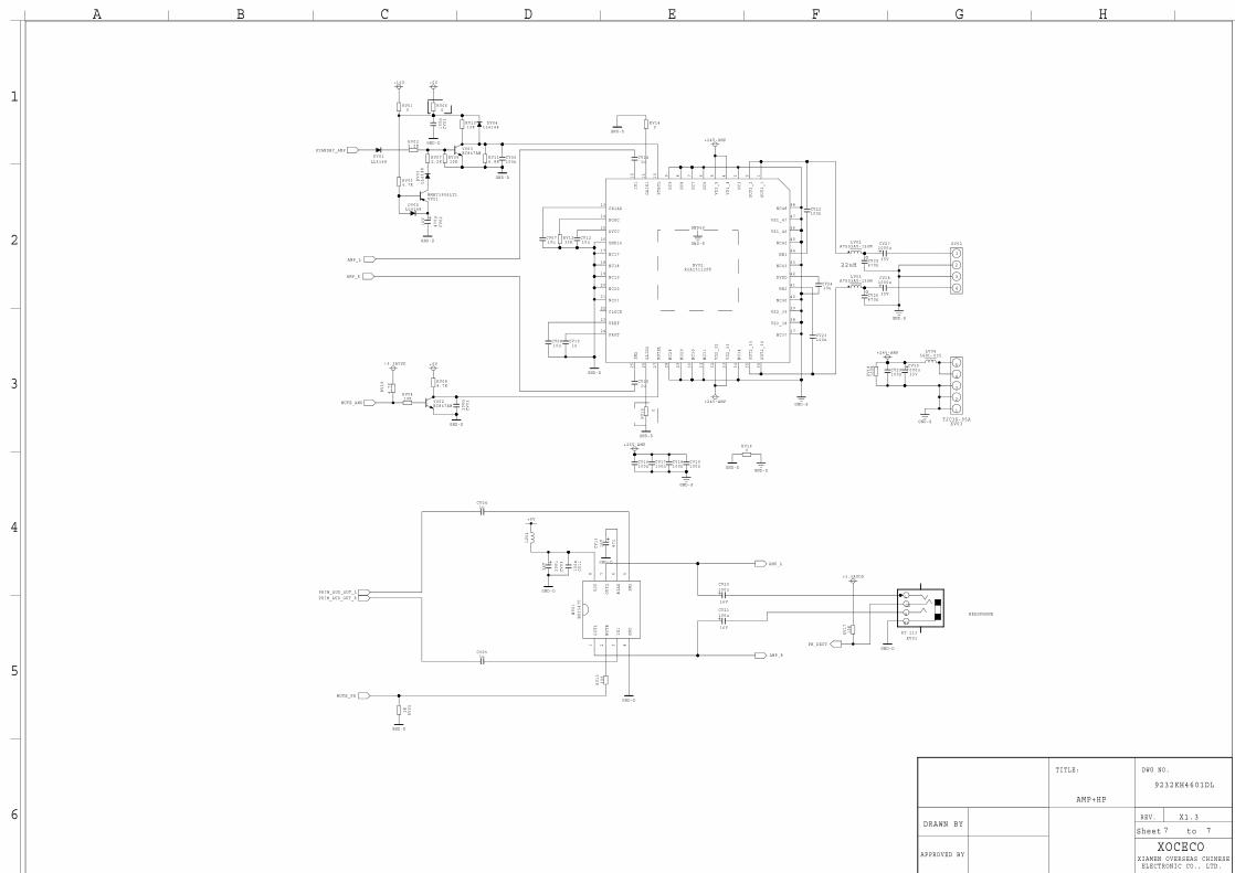
Sheet toDRAWN BY
7 7
X1.3
AMP+HP
9232KH4601DL
XOCECOXIAMEN OVERSEAS CHINESE ELECTRONIC CO., LTD.
TITLE: DWG NO.
REV.
APPROVED BY
22uH
CV271000u
35V
+24V-AMP
GND-D
NV02R2A15112FP
1OUT1_1
2OUT1_2
3NC3
4VD1_4
5VD1_5
6NC6
7NC7
8NC8
9NC9
10
STBYL
11
GAIN1
12
IN1
13CBIAS
14ROSC
15AVCC
16GND16
17NC17
18NC18
19NC19
20NC20
21NC21
22CLOCK
23VREF
24PROT
25
IN2
26
GAIN2
27
MUTEL
28
NC28
29
NC29
30
NC30
31
NC31
32
VD2_32
33
VD2_33
34
NC34
35
OUT2_35
36
OUT2_36
37NC37
38VS2_38
39VS2_39
40NC40
41HB2
42DVDD
43NC43
44HB1
45NC45
46VS1_46
47VS1_47
48NC48
GND49
GND-D
XV03TJC3S-05A
1
2
3
4
5
NV01
BH3547F
1OUT1
2MUTE
3IN1
4GND
5IN2
6BIAS
7OUT2
8VCC
GND-D
AMP_R
CV26470n
GND-D
CV18100n
RV160
DV04LL4148
LV04LSDL-035
GND-D
PRIM_AUD_OUT_R
CV301000u35V
GND-D
+24V-AMP
CV13
47u
16V
GND-S
CV25470n
VV03BC847AW
STANDBY_AMP
GND-S
+5V
GND-S
MUTE_AMP
PRIM_AUD_OUT_L
PH_DECT
GND-S
LV03A7503AY-150M
+24V-AMP
CV17100n
VV02BC847AW
AMP_R
DV01LL4148
CV16100n
+5V
+24V-AMP
GND-D
+12V
GND-D
GND-D
GND-D
CV29100n
GND-S
+5V
GND-D
LV01
MUTE_PH
LV02A7503AY-150M
AMP_L
CV281000u
35V
GND-D
+3.3AVDD
GND-S
XV01ST-113
R
G2
L
G5
AMP_L
DV02LL4148
CV19100n
GND-D
XV02
1
2
3
4
CV02
470u
16V
DV03
LL4148
CV20100u
16V
CV21100u
16V
CV09
100u
16V
+3.3AVDD
RV140
RV15 0
RV060
RV010
RV034.7K
RV084.7K
RV19
4.7K
RV0910K
RV17
10K
RV0410K
RV1010K
RV05
1K
RV116.8K
RV1233K
RV13
100
CV0710u
CV1210u
CV0810u
CV2410u
CV041u
CV051u
CV141u
CV151u
CV11
100n
CV03
100n
CV01
100n
CV06100n
RV022.2K
RV072.2K
RV18
100K
VV01MMBT3906LT1
CV101u
CV23100n
CV22100n
HEADPHONE
A B C D E F G H
1
2
3
4
5
6
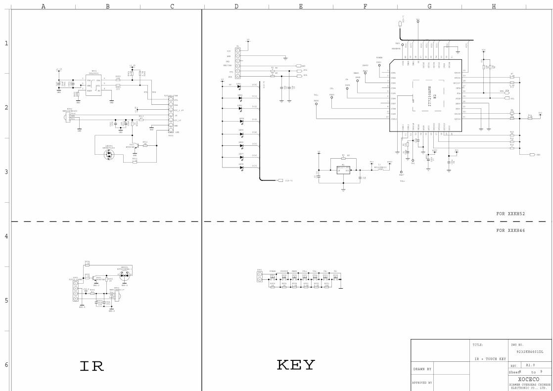
XOCECOSheet to
DRAWN BY
N2
IT7230AFN
9232KH4601DL
A1.0
IR + TOUCH KEY
98
R
B
SDASCL
D[3]
AVCC
D[5]
D[1]
5V
D[1]
D[3]
D[2]
D[6]
D[0-7]
D[7]
D[0]
D[7]
V33
D[2]
5V
D[4]
D[4]
D[6]
D[5]
D[0]
SDA
+3.3V
GND
R9111.1K
GND
GND
R903100
V901BC847AW
R901
100K
C902
100n
+3.3V
R914
3K
GND
GND
R905
2.7K
C911
100n
N901ISL29001
1VDD
2GND
3REXT
4PD
5SCL
6SDA
GND
C912
22uF
10V
GND
N902HRM138CB5400
VoutGND
Vcc
R902100
R91347
+3.3V
LED901GHZRB703D0
X903
TJC10S-07AW
1
2
3
4
5
6
7
C901
22uF
10V
R904
2.7K
R9123K
C1
12p
5V
PAD3
R810K
C7
100n
LED5
LED4
KEY
PAD8SDA
R30
C4
1u
LED6
C8
100n
R5
10K
SDA
C2
12p
X1
1
2
3
4
5
6
TP1
C5
100p
PAD6
V33
R73.3K
R920K
R120
PAD2
D[0-7]
C3
10u
R144.7K
R111K
SCL
PAD1
R6
10K
V33
LED7
5V
PAD4
PAD5
TP2
V33
PAD7
N1
AS1117-3V3
IN OUT
SCL
AVCC
5V
R10
L1BG1608B121
D[0-7]
KEY
LED1
R135.6K
V33
AVCC
R20
R4
100
LED8
C6
100n
1CIN1
2CIN2
3CIN3
4CIN4
5CIN5
6CIN6
7CIN7
8CIN8
9CIN9
10CIN10
11
CIN11
12
CIN12
13
VSHILD
14
VBIAS
15
AVSS
16
AVCC
17
GPIO12
18
GPIO11
19
GPIO10
20
DVCC
21GPIO9
22GPIO8
23ADD1
24ADD0
25SCLK
26SDA
27INT#
28GPIIO7
29GPIO6
30GPIO5
31
GPIO4
32
DVSS
33
GPIO3
34
GPIO2
35
GPIO1
36
GPIO0
37
NC
38
THD1
39
THD0
40
CIN0
GND
R102K
LED2
LED3
S906
R9061K
R9032.4K
S904
X901
1
2
R9041.5K
S905
R90110K
S901S907
R9051K
R9024.3K
S903 S902V901BC847AW
GND-D
LED901HFT503MPBR-1
R B
GND-D
N902HRM138BB5117
VoutGNDVcc
GND-D
C904100n
C90322uF10V
X901TJC10-04AWT
1
2
3
4
+5V-S
GND-D
R9041.1K
R9023.3K
R9052K
R90347
IR
SDA
LED
VCC_5V
SCL
VCC_3.3V
GND
VCC
GND
MENUNC
IRQ
RESERVE
VOL+
SDA
NC
SCL
VOL-
INPUT
NC
CH+
GND/THD
POWER
CH-
POWER VOL+ CH+SOURCE CH-VOL-MENU
XIAMEN OVERSEAS CHINESE ELECTRONIC CO., LTD.
TITLE: DWG NO.
REV.
APPROVED BY
IR KEY
FOR XXKH52
FOR XXKH46
A B C D E F G H
1
2
3
4
5
6
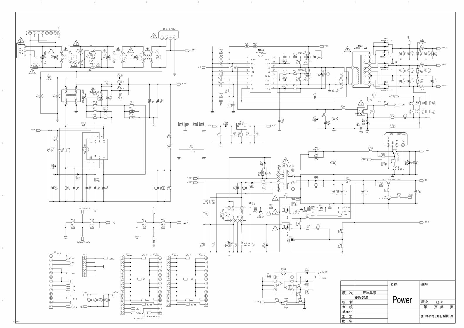
Power
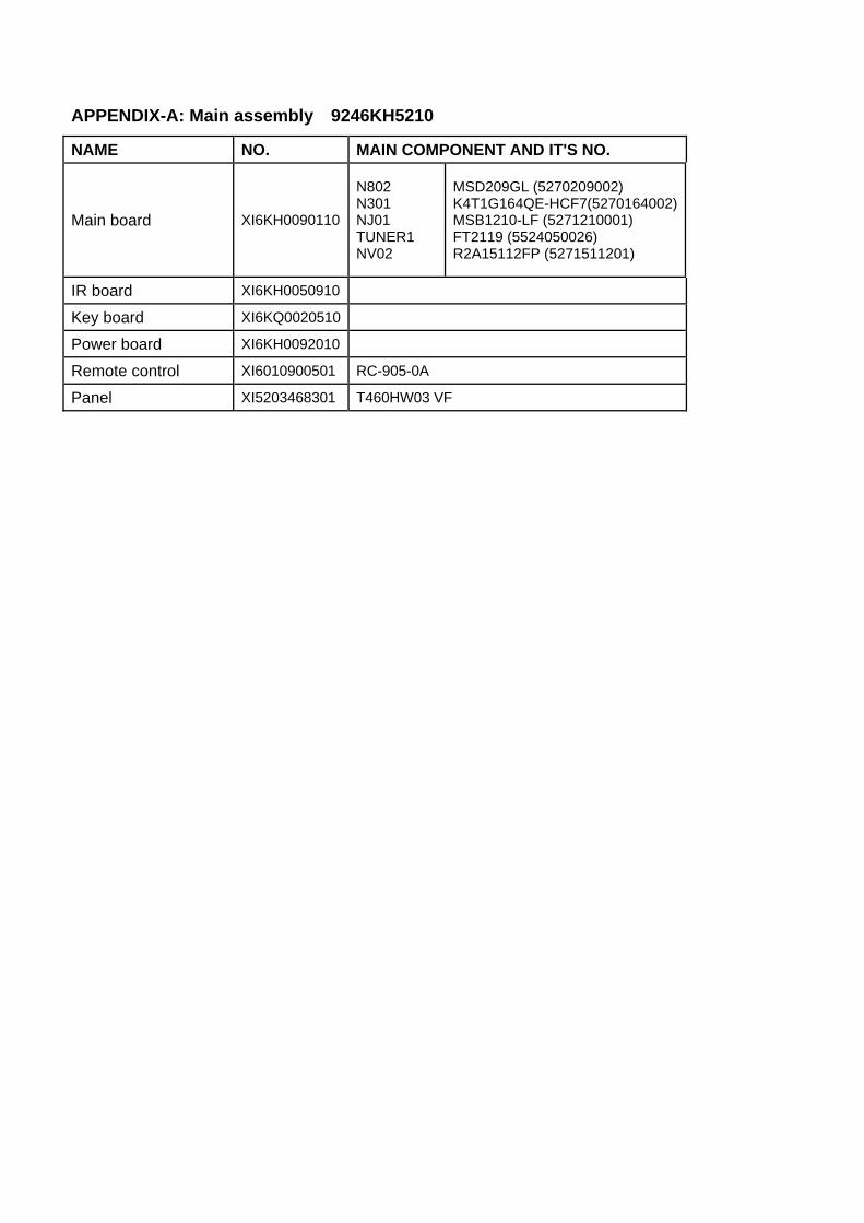
APPENDIX-A: Main assembly 9246KH5210
NAME NO. MAIN COMPONENT AND IT'S NO.
Main board XI6KH0090110
N802 N301 NJ01 TUNER1 NV02
MSD209GL (5270209002) K4T1G164QE-HCF7(5270164002) MSB1210-LF (5271210001) FT2119 (5524050026) R2A15112FP (5271511201)
IR board XI6KH0050910
Key board XI6KQ0020510 Power board XI6KH0092010 Remote control XI6010900501 RC-905-0A
Panel XI5203468301 T460HW03 VF
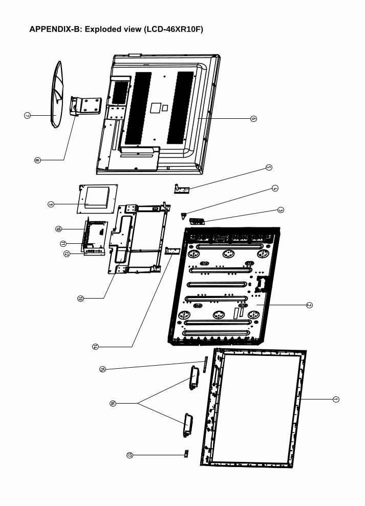
APPENDIX-B: Exploded view (LCD-46XR10F)
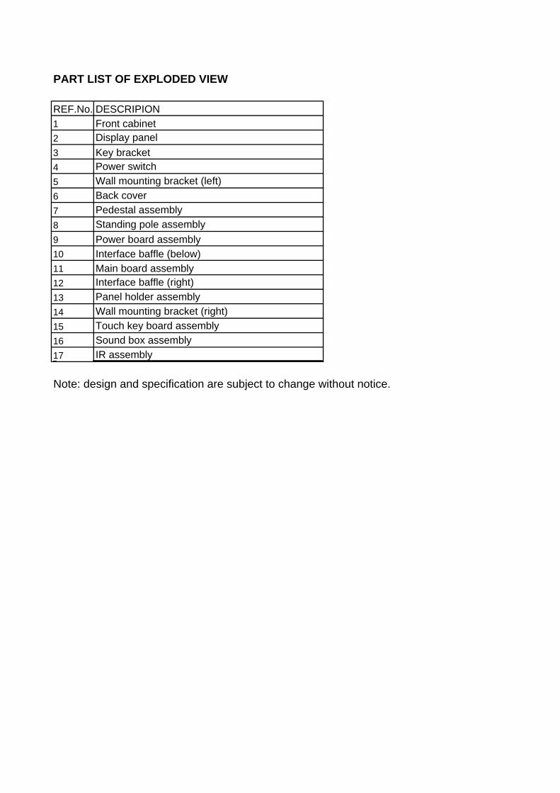
PART LIST OF EXPLODED VIEW
REF.No. DESCRIPION1 Front cabinet 2 Display panel3 Key bracket4 Power switch5 Wall mounting bracket (left)6 Back cover7 Pedestal assembly8 Standing pole assembly9 Power board assembly10 Interface baffle (below)11 Main board assembly12 Interface baffle (right)13 Panel holder assembly14 Wall mounting bracket (right)15 Touch key board assembly16 Sound box assembly17 IR assembly
Note: design and specification are subject to change without notice.
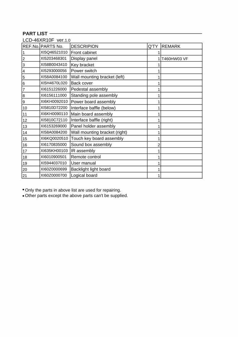
PART LISTLCD-46XR10F ver.1.0REF.No. PARTS No. DESCRIPION Q'TY REMARK1 XI5Q46521010 Front cabinet 12 XI5203468301 Display panel 1 T460HW03 VF3 XI58B0043410 Key bracket 14 XI5293000056 Power switch 15 XI58A0084100 Wall mounting bracket (left) 16 XI5H4670L020 Back cover 17 XI6151226000 Pedestal assembly 18 XI6156111000 Standing pole assembly 19 XI6KH0092010 Power board assembly 110 XI5810D72200 Interface baffle (below) 111 XI6KH0090110 Main board assembly 112 XI5810C72110 Interface baffle (right) 113 XI6153269000 Panel holder assembly 114 XI58A0084200 Wall mounting bracket (right) 115 XI6KQ0020510 Touch key board assembly 116 XI6170835000 Sound box assembly 217 XI635KH00103 IR assembly 118 XI6010900501 Remote control 119 XI5944037010 User manual 120 XI60Z0000699 Backlight light board 121 XI60Z0000700 Logical board 1
Only the parts in above list are used for repairing. Other parts except the above parts can't be supplied.
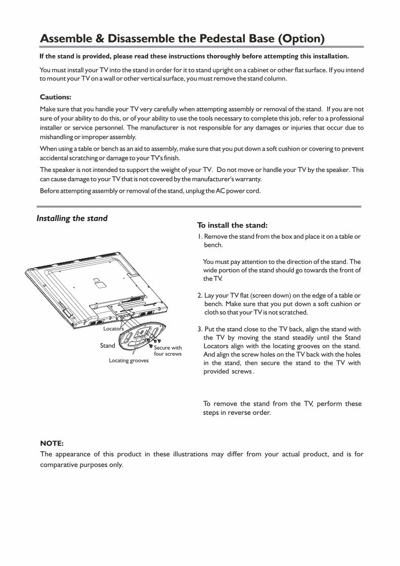
Cautions:
Make sure that you handle your TV very carefully when attempting assembly or removal of the stand. If you are not
sure of your ability to do this, or of your ability to use the tools necessary to complete this job, refer to a professional
installer or service personnel. The manufacturer is not responsible for any damages or injuries that occur due to
mishandling or improper assembly.
When using a table or bench as an aid to assembly, make sure that you put down a soft cushion or covering to prevent
accidental scratching or damage to your TV's finish.
The speaker is not intended to support the weight of your TV. Do not move or handle your TV by the speaker. This
can cause damage to your TV that is not covered by the manufacturer's warranty.
Before attempting assembly or removal of the stand, unplug the AC power cord.
You must install your TV into the stand in order for it to stand upright on a cabinet or other flat surface. If you intend to mount your TV on a wall or other vertical surface, you must remove the stand column.
If the stand is provided, please read these instructions thoroughly before attempting this installation.
NOTE:
The appearance of this product in these illustrations may differ from your actual product, and is for
comparative purposes only.
To remove the stand from the TV, perform these steps in reverse order.
To install the stand:
1. Remove the stand from the box and place it on a table or bench.
You must pay attention to the direction of the stand. The wide portion of the stand should go towards the front of the TV.
2. Lay your TV flat (screen down) on the edge of a table or bench. Make sure that you put down a soft cushion or cloth so that your TV is not scratched.
3. Put the stand close to the TV back, align the stand with the TV by moving the stand steadily until the Stand Locators align with the locating grooves on the stand. And align the screw holes on the TV back with the holes in the stand, then secure the stand to the TV with provided screws .
Installing the stand
Stand
Locators
Locating grooves
Secure with four screws
Assemble & Disassemble the Pedestal Base (Option)
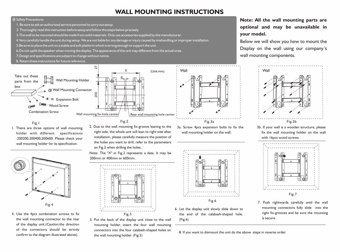

May 2010