Embed Size (px)
Citation preview
No.12015
NATIONAL INSTITUTE FOR MATERIALS SCIENCE
No.12015
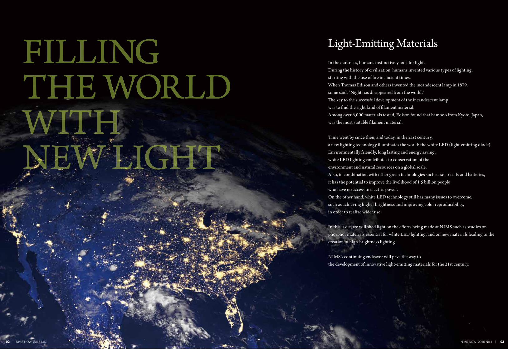
FILLING
THE WORLD
WITH
NEW LIGHT
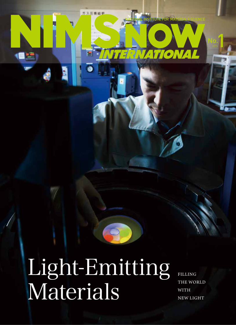
Light-EmittingMaterials
(Dec. 9, 2014) A Signing Ceremony for CCA and ICGP was held at Institut Teknologi Band-ung (ITB) in Bandung, Indonesia. ITB was founded in 1920, later became the Faculty of Engineering in Universitas Indonesia (Univer-sity of Indonesia) for a while, and has been the present ITB since 1959. ITB is one of the universities most popular yet difficult to enter for students in Indonesia, and it is regarded as a model school for engineering education by the
Indonesian Government. ITB delegation headed by Rector Prof. Akhmaloka visited NIMS last September, and expressed a wish for the two agreements. Since this is the first CCA and ICGP with an Indonesia academic institu-tion for NIMS, fur ther enhancement of research collaboration and student exchanges with not only ITB but also other academic institutions in Indonesia is definitely expected.
Hi! I’m really enjoying being in Japan – sometimes it feels as if I’m on an extended vacation! When I arrived last year, NIMS was great in organizing accommodation, language classes and cultural activities, and now I really feel at home. I’m lucky to love my work: my research on metal-organic frameworks offers new excitement every day and NIMS has a fascinating mixture of Japanese and International cultures. I see many differences between the environment here and elsewhere, but ultimately it’s the
people, the individuals, that make a place special. So I’m lucky to have made many friends in NIMS and outside it, who have opened my eyes to new food, experiences and traditions (the picture is of me helping to plant rice at another NIMS staff’s paddy field!). My dream as a scientist is actually not to win a Nobel Prize or anything like that: I want to be happy and for the people around me to be happy too. Then the science will take care of itself.
NIMS signs a Comprehensive Collaborative Agreement (CCA) and an International Cooperative Graduate Program (ICGP) Agreement with Institut Teknologi Bandung, Indonesia
© 2015 All rights reserved by the National Institute for Materials Science
National Institute for Materials ScienceNIMS NOW International 2015. Vol.13 No.1
Percentage of WastePaper pulp 100%
http://www.nims.go.jp/eng/publicity/nimsnow/
To subscribe, contact:Dr. Kazuo Nakamura, PublisherPublic Relations Office, NIMS1-2-1 Sengen, Tsukuba, Ibaraki, 305-0047 JAPANPhone: +81-29-859-2026, Fax: +81-29-859-2017Email: [email protected]
Report on the 6th Tsukuba International Coating Symposium
(Dec 4th and 5th, 2014) The 6th Tsukuba Inter-national Coating Symposium (TICS 2014) was held at the WPI-MANA Auditorium. This symposium, co-organized by NIMS and the National Institute of Advanced Industrial Science and Technology (AIST), has been held every two years, in order to discuss how coat-ing research activities will contribute to science and technology, through the introduction of research topics currently investigated in Tsuku-ba, as well as presentations by world-leading researchers. In this symposium, partly co-orga-nized by MANA, the focus was on the coatings for 2D, 3D additive manufacturing, coatings for infrastructure, thermal and environmental barrier coatings, and functional ceramics and nanocrystal coatings. We had 33 oral presenta-
tions and 122 participants in total, with very active interactions among them, confirming
that this symposium was a very fruitful one for coating researchers.
Hamish YeungUnited KingdomFebruary 2014 – presentICYS-MANA researcher
1
2
Group photo of thesymposium participants
ITB Rector Prof.Akhmaloka (right) and NIMS Presi-dent Prof. Ushioda signing the agreements
02 NIMS NOW 2015 No.1 03NIMS NOW 2015 No.1
FILLING THE WORLD WITH NEW LIGHT
Identity of light
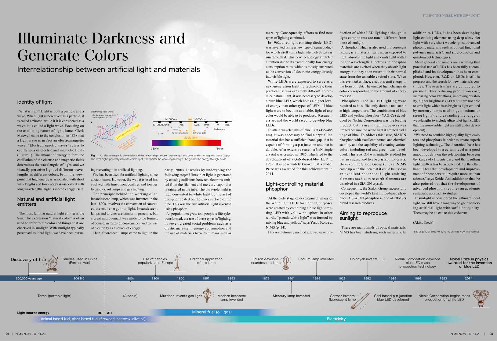
What is light? Light is both a particle and a wave. When light is perceived as a particle, it is called a photon, while if it is considered as a wave, it is called a light wave. Focusing on the oscillating nature of light, James Clerk Maxwell came to the conclusion in 1868 that a light wave is in fact an electromagnetic wave. “Electromagnetic waves” refers to oscillations of electric and magnetic fields (Figure 1). The amount of energy to form the oscillation of the electric and magnetic fields determines the wavelengths of light, and we visually perceive light of different wave-lengths as different colors. From the view-point that high energy is associated with short wavelengths and low energy is associated with long wavelengths, light is indeed energy itself.
Natural and artificial light emitters The most familiar natural light emitter is the Sun. The expression “natural color” is often used to refer to the colors of things that are observed in sunlight. With sunlight typically perceived as ideal light, we have been pursu-
ing recreating it in artificial lighting. Fire has been used for artificial lighting since ancient times. However, the way it is used has evolved with time, from bonfires and torches to candles, oil lamps and gas lighting. The principle behind the working of an incandescent lamp, which was invented in the late 1800s, involves the conversion of saturat-ed thermal energy into light. Incandescent lamps and torches are similar in principle, but a great improvement was made to the former, of course, in terms of convenience and the use of electricity as a source of energy. Then, fluorescent lamps came to light in the
early 1900s. It works by undergoing the following steps: Ultraviolet light is generated by causing collisions between electrons emit-ted from the filament and mercury vapor that is saturated in the tube. The ultraviolet light is then converted to white light by the act of phosphor coated on the inner surface of the tube. This was the first artificial light invented using phosphor. As populations grew and people’s lifestyles transformed, the use of these types of lighting, however, created social problems such as a drastic increase in energy consumption and the use of materials toxic to humans such as
mercury. Consequently, efforts to find new types of lighting continued. In 1962, a red light-emitting diode (LED) was invented using a new type of semiconduc-tor which itself emits light when electricity is run through it. This new technology attracted attention due to its exceptionally low energy consumption rates, which is mostly attributed to the conversion of electronic energy directly into visible light. While LEDs were expected to serve as a next-generation lighting technology, their practical use was extremely difficult. To pro-duce natural light, it was necessary to develop a pure blue LED, which holds a higher level of energy than other types of LEDs. If blue light were to become available, light of any color would be able to be produced. Research-ers around the world raced to develop blue LEDs. To attain wavelengths of blue light (455-485 nm), it was necessary to find a crystalline material that has a sufficient band gap, that is capable of forming a p-n junction and that is durable. After extensive search, a GaN single crystal was created in 1985, which led to the development of a GaN-based blue LED in 1989. It is now widely known that a Nobel Prize was awarded for this achievement in 2014.
Light-controlling material, phosphor
“At the early stage of development, many of the white light LEDs for lighting purposes were created by combining a blue light-emit-ting LED with yellow phosphor. In other words, “pseudo white light” was formed by mixing blue and yellow.” says Yasuo Koide at NIMS (p. 14). This revolutionary method allowed easy pro-
duction of white LED lighting although its light components are much different from those of sunlight. A phosphor, which is also used in fluorescent lamps, is a material that, when exposed to light, absorbs the light and emits light with a longer wavelength. Electrons in phosphor materials are excited when they absorb light energy, but they soon return to their normal state from the unstable excited state. When this event takes place, electrons emit energy in the form of light. The emitted light changes its color corresponding to the amount of energy released. Phosphors used in LED lighting were required to be sufficiently durable and stable at high temperature. The combination of blue LED and yellow phosphor (YAG:Ce) devel-oped by Nichia Corporation was the leading product, but its use in lighting devices was limited because the white light it emitted had a tinge of blue. To address this issue, SiAlON phosphor, with excellent thermal and chemical stability and the capability of creating various colors including red and green, was devel-oped. This SiAlON was initially studied for use in engine and heat-resistant materials. However, the Sialon Group (p. 6) at NIMS came up with the idea that it could be used as an excellent phosphor if light-emitting elements such as rare earth elements are dissolved in a SiAlON crystal. Consequently, the Sialon Group successfully developed the world’s first nitride-based phos-phor. A SiAlON phosphor is one of NIMS’s proud research products.
Aiming to reproduce sunlight
There are many kinds of optical materials. NIMS has been studying such materials. In
addition to LEDs, it has been developing light-emitting elements using deep ultraviolet light with very short wavelengths, advanced photonic materials such as optical functional polymer materials*, and single-photon and quantum dot technologies. Most general consumers are assuming that practical use of LEDs has been fully accom-plished and its development has been com-pleted. However, R&D on LEDs is still in progress and the search for new materials con-tinues. These activities are conducted to pursue further reducing production cost, increasing color variations, improving durabil-ity, higher brightness (LEDs still are not able to emit light which is as bright as light emitted by mercury lamps used in gymnasiums or street lights), and expanding the range of wavelengths to include ultraviolet light (LEDs that use non-visible light are still under devel-opment). “We need to combine high-quality light emit-ters and phosphors in order to create superb lighting technology. The theoretical base has been developed to a certain level as a good amount of data on the relationship between the kinds of elements used and the resulting light emitters has been collected. On the other hand, I feel that development and improve-ment of phosphors still require more art than science,” says Koide. And addition to that, he also pointed out that the development of advanced phosphors requires an academic systematic approach to studies. If sunlight is considered the ultimate ideal light, we still have a long way to go in achiev-ing artificial light with sufficient quality. There may be no end to this endeavor.
(Akiko Ikeda)
*See page 12 of Issue No. 6, Vol. 12 of NIMS NOW International.
Illuminate Darkness and Generate ColorsInterrelationship between artificial light and materials
500,000 years ago 206 B.C. 1300 1800 1851 1853 1879 1901 1919 1926 1962 1989 1993 1993 2014(800)
Discovery of fire
Torch (portable light)
Candles used in China(Former Han)
(Aladdin)
Use of candles popularized in Europe
Murdoch invents gas light
Practical applicationof arc lamp
Modern kerosenelamp invented
Edison developsincandescent lamp
Mercury lamp invented
Sodium lamp invented
Germer inventsfluorescent lamp
Holonyak invents LED Nichia Corporation developsblue LED mass
production technology
Nichia Corporation begins massproduction of white LED
GaN-based p-n junctionblue LED developed
Nobel Prize in physicsawarded for the invention
of blue LED
Light source energy
Animal-based fuel, plant-based fuel (firewood, beeswax, olive oil) Electricity
Mineral fuel (oil, gas)
Fig. 1. An electromagnetic wave (left) and the relationship between wavelength and color of electromagnetic wave (right). The term “light” generally refers to visible light. The shorter the wavelength of light, the greater the energy the light holds.
BC AD
x
field H
y
Oscillation of electric field E and magnetic field H
Direction of traveling light
Wavelength of the
electromagnetic
wave (light)
Electromagnetic wave
γ ray
x rayUltraviolet light Infrared light
Radio wave
380nm 780nm
1/1000000nm 1nm 1mm1μm 1km1m
1/1000nm 1/1000mm
visible light
field E
04 NIMS NOW 2015 No.1 05NIMS NOW 2015 No.1
06 NIMS NOW 2015 No.1
350 450 550 650 750
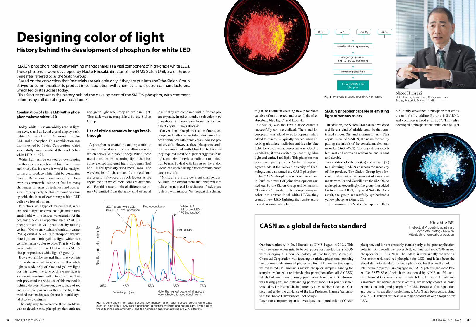
Combination of a blue LED with a phos-phor makes a white LED
Today, white LEDs are widely used in light-ing devices and as liquid crystal display back-lights. Current white LEDs consist of a blue LED and a phosphor. This combination was first invented by Nichia Corporation, which successfully commercialized the world’s first white LED in 1996. White light can be created by overlapping the three primary colors of light (red, green and blue). So, it seems it would be straight-forward to produce white light by combining three LEDs that emit these three colors. How-ever, its commercialization in fact has many challenges in terms of technical and cost is-sues. Consequently, Nichia Corporation came up with the idea of combining a blue LED with a yellow phosphor. Phosphors are a type of material that, when exposed to light, absorbs that light and in turn, emits light with a longer wavelength. At the beginning, Nichia Corporation used a YAG:Ce phosphor which was produced by adding cerium (Ce) to an yttrium-aluminum-garnet (YAG) crystal. A YAG:Ce phosphor absorbs blue light and emits yellow light, which is a complementary color to blue. That is why the combination of a blue LED with a YAG:Ce phosphor produces white light (Figure 1). However, unlike natural light that consists of a wide range of wavelengths, this white light is made only of blue and yellow light. For this reason, the tone of this white light is somewhat unnatural with a tinge of blue. This trait prevented the wide use of this method in lighting devices. Moreover, due to lack of red and green components in this white light, the method was inadequate for use in liquid crys-tal display backlights. The only way to overcome these problems was to develop new phosphors that emit red
and green light when they absorb blue light. This task was accomplished by the Sialon Group.
Use of nitride ceramics brings break-through
A phosphor is created by adding a minute amount of metal ions to a crystalline ceramic, which serves as a parent body. When these metal ions absorb incoming light, they be-come excited and emit light. Europium (Eu) and Ce are typically used metal ions. The wavelengths of light emitted from metal ions are greatly influenced by such factors as the crystal field in which metal ions are distribut-ed. “For this reason, light of different colors may be emitted from the same kind of metal
ions if they are combined with different par-ent crystals. In other words, to develop new phosphors, it is necessary to search for new parent crystals,” says Hirosaki. Conventional phosphors used in fluorescent lamps and cathode-ray tube televisions had been combined with oxide ceramic-based par-ent crystals. However, these phosphors could not be combined with blue LEDs because they required input of higher energy than blue light, namely, ultraviolet radiation and elec-tron beams. To deal with this issue, the Sialon Group considered using nitride ceramic-based parent crystals. “Nitrides are more covalent than oxides. As such, the crystal field that encompasses light-emitting metal ions changes if oxides are replaced with nitrides. We thought this change
might be useful in creating new phosphors capable of emitting red and green light when absorbing blue light,” said Hirosaki. CaAlSiN3 was the first nitride ceramic successfully commercialized. The metal ion europium was added to it. Europium, when added to oxides, is typically excited when ab-sorbing ultraviolet radiation and it emits blue light. However, when europium was added to CaAlSiN3, it was excited by incoming blue light and emitted red light. This phosphor was developed jointly by the Sialon Group and Kyota Ueda at the Tokyo University of Tech-nology, and was named the CASN phosphor. The CASN phosphor was commercialized in 2008 as a result of joint development car-ried out by the Sialon Group and Mitsubishi Chemical Corporation. By incorporating red color into conventional white LEDs, they created new LED lighting that emits more natural, warmer white light.
SiAlON phosphor capable of emitting light of various colors
In addition, the Sialon Group also developed a different kind of nitride ceramic that con-tained silicon (Si) and aluminum (Al). This crystal is called SiAlON, the name formed by putting the initials of the constituent elements in order (Si-Al-O-N). The crystal has excel-lent heat and corrosion resistance, and is hard and durable. An addition of calcium (Ca) and yttrium (Y) to a sintering SiAlON enhances the reactivity of the product. The Sialon Group hypothe-sized that a partial replacement of these ele-ments with Eu and Ce will turn the SiAlON to a phosphor. Accordingly, the group first added Eu to an α-SiAlON, a type of SiAlON. As a result, the group successfully synthesized a yellow phosphor (Figure 2). Furthermore, the Sialon Group and DEN-
KA jointly developed a phosphor that emits green light by adding Eu to a β-SiAlON, and commercialized it in 2007. They also developed a phosphor that emits orange light
07NIMS NOW 2015 No.1
SiAlON phosphors hold overwhelming market shares as a vital component of high-grade white LEDs. These phosphors were developed by Naoto Hirosaki, director of the NIMS Sialon Unit, Sialon Group (hereafter referred to as the Sialon Group). Based on the conviction that “materials are valuable only if they are put into use,” the Sialon Group strived to commercialize its product in collaboration with chemical and electronics manufacturers, which led to its success today. This feature presents the history behind the development of the SiAlON phosphor, with comment columns by collaborating manufacturers.
Naoto HirosakiUnit director, Sialon Unit, Environment and Energy Materials Division, NIMS
Our interaction with Dr. Hirosaki at NIMS began in 2003. This was the time when nitride-based phosphors including SiAlON were emerging as a new technology. At that time, we, Mitsubishi Chemical Corporation was focusing on nitride phosphors, pursuing the commercialization of phosphors for LED, and in this regard we evaluated Dr. Hirosaki’s nitride phosphor samples. Among the samples evaluated, a red nitride phosphor (thereafter called CASN) which had been found through joint research in which Dr. Hirosaki was taking part, had outstanding performance. This joint research was led by Dr. Kyota Uheda (currently at Mitsubishi Chemical Cor-poration) under the guidance of the late Professor Hajime Yamamo-to at the Tokyo University of Technology.Later, our company began to investigate mass production of CASN
phosphor, and it went smoothly thanks partly to its great application potential. As a result, we successfully commercialized CASN as red phosphor for LED in 2008. The CASN is substantially the world’s first commercialized red phosphor for LED, and it has been the global de facto standard for such phosphor. Further, in the field of intellectual property I am engaged in, CASN patents (Japanese Pat-ent No. 3837588 etc.) which are co-owned by NIMS and Mitsubi-shi Chemical Corporation and in which Drs. Hirosaki, Uheda and Yamamoto are named as the inventors, are widely known as basic patents concerning red phosphor for LED. Because of its reputation and due to its excellent performance, CASN has been contributing to our LED related business as a major product of our phosphor for LED.
Hitoshi ABEIntellectual Property Department
Corporate Strategy DivisionMitsubishi Chemical Corporation
CASN as a global de facto standard
Designing color of lightHistory behind the development of phosphors for white LED
Relat
ive e
miss
ion
inte
nsity
LED Pseudo-white LED(blue LED + YAG phosphor)
Fluorescent lamp White LED(Ultraviolet LED + RGB phosphor)
Natural light
Wavelength (nm) Note: the highest peaks of all spectra were adjusted to have equal height
Fig. 1. Difference in emission spectra. Comparison of emission spectra among white LEDs such as “blue LED + YAG-based phosphor,” a fluorescent lamp and natural light. Even if all of these technologies emit white light, their emission spectrum profiles are very different.
Fig. 2. Synthesis procedure of SiAION phosphor
08 NIMS NOW 2015 No.1 09NIMS NOW 2015 No.1
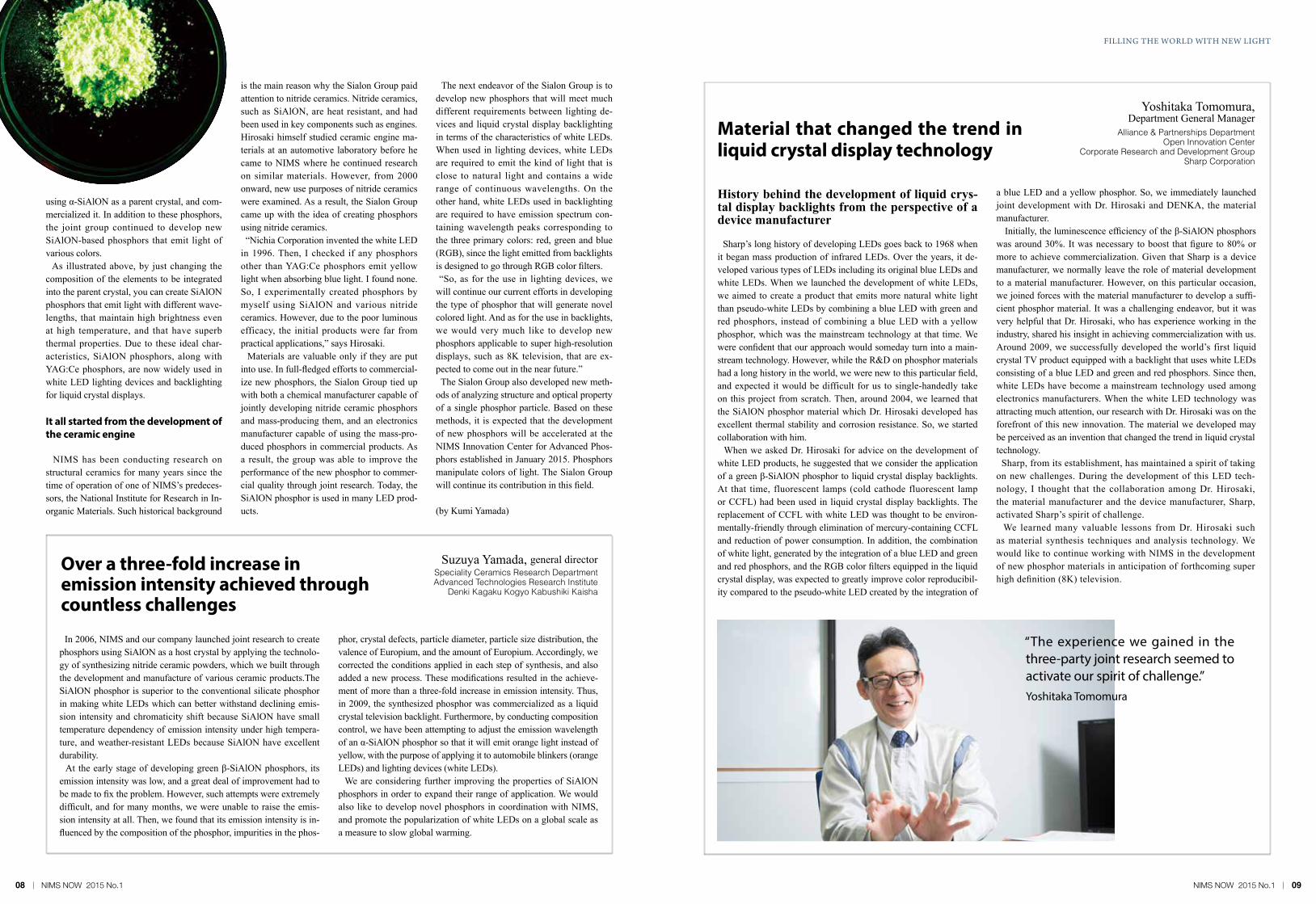
using α-SiAlON as a parent crystal, and com-mercialized it. In addition to these phosphors, the joint group continued to develop new SiAlON-based phosphors that emit light of various colors. As illustrated above, by just changing the composition of the elements to be integrated into the parent crystal, you can create SiAlON phosphors that emit light with different wave-lengths, that maintain high brightness even at high temperature, and that have superb thermal properties. Due to these ideal char-acteristics, SiAlON phosphors, along with YAG:Ce phosphors, are now widely used in white LED lighting devices and backlighting for liquid crystal displays.
It all started from the development of the ceramic engine
NIMS has been conducting research on structural ceramics for many years since the time of operation of one of NIMS’s predeces-sors, the National Institute for Research in In-organic Materials. Such historical background
is the main reason why the Sialon Group paid attention to nitride ceramics. Nitride ceramics, such as SiAlON, are heat resistant, and had been used in key components such as engines.Hirosaki himself studied ceramic engine ma-terials at an automotive laboratory before he came to NIMS where he continued research on similar materials. However, from 2000 onward, new use purposes of nitride ceramics were examined. As a result, the Sialon Group came up with the idea of creating phosphors using nitride ceramics. “Nichia Corporation invented the white LED in 1996. Then, I checked if any phosphors other than YAG:Ce phosphors emit yellow light when absorbing blue light. I found none. So, I experimentally created phosphors by myself using SiAlON and various nitride ceramics. However, due to the poor luminous efficacy, the initial products were far from practical applications,” says Hirosaki. Materials are valuable only if they are put into use. In full-fledged efforts to commercial-ize new phosphors, the Sialon Group tied up with both a chemical manufacturer capable of jointly developing nitride ceramic phosphors and mass-producing them, and an electronics manufacturer capable of using the mass-pro-duced phosphors in commercial products. As a result, the group was able to improve the performance of the new phosphor to commer-cial quality through joint research. Today, the SiAlON phosphor is used in many LED prod-ucts.
The next endeavor of the Sialon Group is to develop new phosphors that will meet much different requirements between lighting de-vices and liquid crystal display backlighting in terms of the characteristics of white LEDs. When used in lighting devices, white LEDs are required to emit the kind of light that is close to natural light and contains a wide range of continuous wavelengths. On the other hand, white LEDs used in backlighting are required to have emission spectrum con-taining wavelength peaks corresponding to the three primary colors: red, green and blue (RGB), since the light emitted from backlights is designed to go through RGB color filters. “So, as for the use in lighting devices, we will continue our current efforts in developing the type of phosphor that will generate novel colored light. And as for the use in backlights, we would very much like to develop new phosphors applicable to super high-resolution displays, such as 8K television, that are ex-pected to come out in the near future.” The Sialon Group also developed new meth-ods of analyzing structure and optical property of a single phosphor particle. Based on these methods, it is expected that the development of new phosphors will be accelerated at the NIMS Innovation Center for Advanced Phos-phors established in January 2015. Phosphors manipulate colors of light. The Sialon Group will continue its contribution in this field.
(by Kumi Yamada)
In 2006, NIMS and our company launched joint research to create phosphors using SiAlON as a host crystal by applying the technolo-gy of synthesizing nitride ceramic powders, which we built through the development and manufacture of various ceramic products.The SiAlON phosphor is superior to the conventional silicate phosphor in making white LEDs which can better withstand declining emis-sion intensity and chromaticity shift because SiAlON have small temperature dependency of emission intensity under high tempera-ture, and weather-resistant LEDs because SiAlON have excellent durability. At the early stage of developing green β-SiAlON phosphors, its emission intensity was low, and a great deal of improvement had to be made to fix the problem. However, such attempts were extremely difficult, and for many months, we were unable to raise the emis-sion intensity at all. Then, we found that its emission intensity is in-fluenced by the composition of the phosphor, impurities in the phos-
phor, crystal defects, particle diameter, particle size distribution, the valence of Europium, and the amount of Europium. Accordingly, we corrected the conditions applied in each step of synthesis, and also added a new process. These modifications resulted in the achieve-ment of more than a three-fold increase in emission intensity. Thus, in 2009, the synthesized phosphor was commercialized as a liquid crystal television backlight. Furthermore, by conducting composition control, we have been attempting to adjust the emission wavelength of an α-SiAlON phosphor so that it will emit orange light instead of yellow, with the purpose of applying it to automobile blinkers (orange LEDs) and lighting devices (white LEDs). We are considering further improving the properties of SiAlON phosphors in order to expand their range of application. We would also like to develop novel phosphors in coordination with NIMS, and promote the popularization of white LEDs on a global scale as a measure to slow global warming.
History behind the development of liquid crys-tal display backlights from the perspective of a device manufacturer
Sharp’s long history of developing LEDs goes back to 1968 when it began mass production of infrared LEDs. Over the years, it de-veloped various types of LEDs including its original blue LEDs and white LEDs. When we launched the development of white LEDs, we aimed to create a product that emits more natural white light than pseudo-white LEDs by combining a blue LED with green and red phosphors, instead of combining a blue LED with a yellow phosphor, which was the mainstream technology at that time. We were confident that our approach would someday turn into a main-stream technology. However, while the R&D on phosphor materials had a long history in the world, we were new to this particular field, and expected it would be difficult for us to single-handedly take on this project from scratch. Then, around 2004, we learned that the SiAlON phosphor material which Dr. Hirosaki developed has excellent thermal stability and corrosion resistance. So, we started collaboration with him. When we asked Dr. Hirosaki for advice on the development of white LED products, he suggested that we consider the application of a green β-SiAlON phosphor to liquid crystal display backlights. At that time, fluorescent lamps (cold cathode fluorescent lamp or CCFL) had been used in liquid crystal display backlights. The replacement of CCFL with white LED was thought to be environ-mentally-friendly through elimination of mercury-containing CCFL and reduction of power consumption. In addition, the combination of white light, generated by the integration of a blue LED and green and red phosphors, and the RGB color filters equipped in the liquid crystal display, was expected to greatly improve color reproducibil-ity compared to the pseudo-white LED created by the integration of
a blue LED and a yellow phosphor. So, we immediately launched joint development with Dr. Hirosaki and DENKA, the material manufacturer. Initially, the luminescence efficiency of the β-SiAlON phosphors was around 30%. It was necessary to boost that figure to 80% or more to achieve commercialization. Given that Sharp is a device manufacturer, we normally leave the role of material development to a material manufacturer. However, on this particular occasion, we joined forces with the material manufacturer to develop a suffi-cient phosphor material. It was a challenging endeavor, but it was very helpful that Dr. Hirosaki, who has experience working in the industry, shared his insight in achieving commercialization with us. Around 2009, we successfully developed the world’s first liquid crystal TV product equipped with a backlight that uses white LEDs consisting of a blue LED and green and red phosphors. Since then, white LEDs have become a mainstream technology used among electronics manufacturers. When the white LED technology was attracting much attention, our research with Dr. Hirosaki was on the forefront of this new innovation. The material we developed may be perceived as an invention that changed the trend in liquid crystal technology. Sharp, from its establishment, has maintained a spirit of taking on new challenges. During the development of this LED tech-nology, I thought that the collaboration among Dr. Hirosaki, the material manufacturer and the device manufacturer, Sharp, activated Sharp’s spirit of challenge. We learned many valuable lessons from Dr. Hirosaki such as material synthesis techniques and analysis technology. We would like to continue working with NIMS in the development of new phosphor materials in anticipation of forthcoming super high definition (8K) television.
Yoshitaka Tomomura, Department General Manager
Alliance & Partnerships DepartmentOpen Innovation Center
Corporate Research and Development GroupSharp Corporation
Material that changed the trend in liquid crystal display technology
“The experience we gained in the three-party joint research seemed to activate our spirit of challenge.”Yoshitaka Tomomura
FILLING THE WORLD WITH NEW LIGHT
Suzuya Yamada, general directorSpeciality Ceramics Research DepartmentAdvanced Technologies Research Institute
Denki Kagaku Kogyo Kabushiki Kaisha
Over a three-fold increase in emission intensity achieved throughcountless challenges
10 NIMS NOW 2015 No.1 11NIMS NOW 2015 No.1
Think outside the box
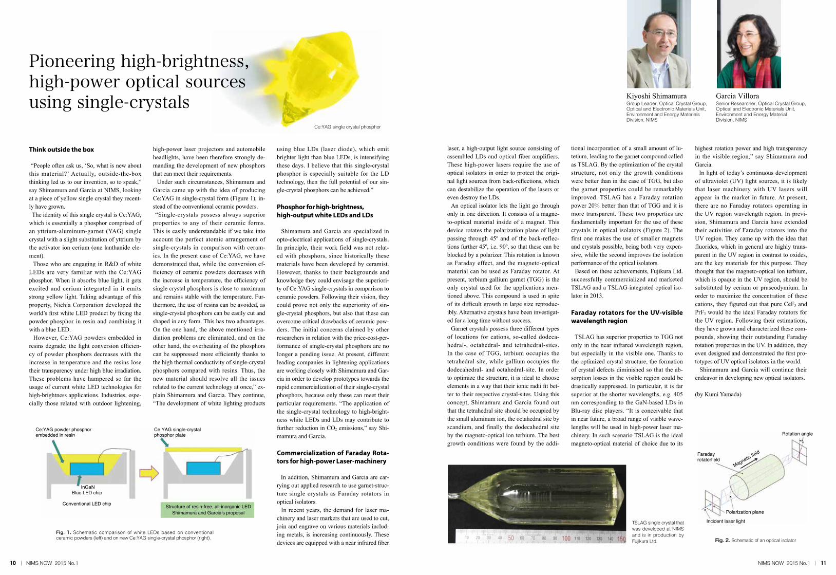
“People often ask us, ‘So, what is new about this material?’ Actually, outside-the-box thinking led us to our invention, so to speak,” say Shimamura and Garcia at NIMS, looking at a piece of yellow single crystal they recent-ly have grown. The identity of this single crystal is Ce:YAG, which is essentially a phosphor comprised of an yttrium-aluminum-garnet (YAG) single crystal with a slight substitution of yttrium by the activator ion cerium (one lanthanide ele-ment). Those who are engaging in R&D of white LEDs are very familiar with the Ce:YAG phosphor. When it absorbs blue light, it gets excited and cerium integrated in it emits strong yellow light. Taking advantage of this property, Nichia Corporation developed the world’s first white LED product by fixing the powder phosphor in resin and combining it with a blue LED. However, Ce:YAG powders embedded in resins degrade; the light conversion efficien-cy of powder phosphors decreases with the increase in temperature and the resins lose their transparency under high blue irradiation. These problems have hampered so far the usage of current white LED technologies for high-brightness applications. Industries, espe-cially those related with outdoor lightening,
high-power laser projectors and automobile headlights, have been therefore strongly de-manding the development of new phosphors that can meet their requirements. Under such circumstances, Shimamura and Garcia came up with the idea of producing Ce:YAG in single-crystal form (Figure 1), in-stead of the conventional ceramic powders. “Single-crystals possess always superior properties to any of their ceramic forms. This is easily understandable if we take into account the perfect atomic arrangement of single-crystals in comparison with ceram-ics. In the present case of Ce:YAG, we have demonstrated that, while the conversion ef-ficiency of ceramic powders decreases with the increase in temperature, the efficiency of single crystal phosphors is close to maximum and remains stable with the temperature. Fur-thermore, the use of resins can be avoided, as single-crystal phosphors can be easily cut and shaped in any form. This has two advantages.On the one hand, the above mentioned irra-diation problems are eliminated, and on the other hand, the overheating of the phosphors can be suppressed more efficiently thanks to the high thermal conductivity of single-crystal phosphors compared with resins. Thus, the new material should resolve all the issues related to the current technology at once,” ex-plain Shimamura and Garcia. They continue, “The development of white lighting products
using blue LDs (laser diode), which emit brighter light than blue LEDs, is intensifying these days. I believe that this single-crystal phosphor is especially suitable for the LD technology, then the full potential of our sin-gle-crystal phosphors can be achieved.”
Phosphor for high-brightness, high-output white LEDs and LDs
Shimamura and Garcia are specialized in opto-electrical applications of single-crystals. In principle, their work field was not relat-ed with phosphors, since historically these materials have been developed by ceramist. However, thanks to their backgrounds and knowledge they could envisage the superiori-ty of Ce:YAG single-crystals in comparison to ceramic powders. Following their vision, they could prove not only the superiority of sin-gle-crystal phosphors, but also that these can overcome critical drawbacks of ceramic pow-ders. The initial concerns claimed by other researchers in relation with the price-cost-per-formance of single-crystal phosphors are no longer a pending issue. At present, different leading companies in lightening applications are working closely with Shimamura and Gar-cia in order to develop prototypes towards the rapid commercialization of their single-crystal phosphors, because only these can meet their particular requirements. “The application of the single-crystal technology to high-bright-ness white LEDs and LDs may contribute to further reduction in CO2 emissions,” say Shi-mamura and Garcia.
Commercialization of Faraday Rota-tors for high-power Laser-machinery
In addition, Shimamura and Garcia are car-rying out applied research to use garnet-struc-ture single crystals as Faraday rotators in optical isolators. In recent years, the demand for laser ma-chinery and laser markers that are used to cut, join and engrave on various materials includ-ing metals, is increasing continuously. These devices are equipped with a near infrared fiber
laser, a high-output light source consisting of assembled LDs and optical fiber amplifiers. These high-power lasers require the use of optical isolators in order to protect the origi-nal light sources from back-reflections, which can destabilize the operation of the lasers or even destroy the LDs. An optical isolator lets the light go through only in one direction. It consists of a magne-to-optical material inside of a magnet. This device rotates the polarization plane of light passing through 45º and of the back-reflec-tions further 45º, i.e. 90º, so that these can be blocked by a polarizer. This rotation is known as Faraday effect, and the magneto-optical material can be used as Faraday rotator. At present, terbium gallium garnet (TGG) is the only crystal used for the applications men-tioned above. This compound is used in spite of its difficult growth in large size reproduc-ibly. Alternative crystals have been investigat-ed for a long time without success. Garnet crystals possess three different types of locations for cations, so-called dodeca-hedral-, octahedral- and tetrahedral-sites. In the case of TGG, terbium occupies the tetrahedral-site, while gallium occupies the dodecahedral- and octahedral-site. In order to optimize the structure, it is ideal to choose elements in a way that their ionic radii fit bet-ter to their respective crystal-sites. Using this concept, Shimamura and Garcia found out that the tetrahedral site should be occupied by the small aluminum ion, the octahedral site by scandium, and finally the dodecahedral site by the magneto-optical ion terbium. The best growth conditions were found by the addi-
tional incorporation of a small amount of lu-tetium, leading to the garnet compound called as TSLAG. By the optimization of the crystal structure, not only the growth conditions were better than in the case of TGG, but also the garnet properties could be remarkably improved. TSLAG has a Faraday rotation power 20% better than that of TGG and it is more transparent. These two properties are fundamentally important for the use of these crystals in optical isolators (Figure 2). The first one makes the use of smaller magnets and crystals possible, being both very expen-sive, while the second improves the isolation performance of the optical isolators. Based on these achievements, Fujikura Ltd. successfully commercialized and marketed TSLAG and a TSLAG-integrated optical iso-lator in 2013.
Faraday rotators for the UV-visible wavelength region
TSLAG has superior properties to TGG not only in the near infrared wavelength region, but especially in the visible one. Thanks to the optimized crystal structure, the formation of crystal defects diminished so that the ab-sorption losses in the visible region could be drastically suppressed. In particular, it is far superior at the shorter wavelengths, e.g. 405 nm corresponding to the GaN-based LDs in Blu-ray disc players. “It is conceivable that in near future, a broad range of visible wave-lengths will be used in high-power laser ma-chinery. In such scenario TSLAG is the ideal magneto-optical material of choice due to its
highest rotation power and high transparency in the visible region,” say Shimamura and Garcia. In light of today’s continuous development of ultraviolet (UV) light sources, it is likely that laser machinery with UV lasers will appear in the market in future. At present, there are no Faraday rotators operating in the UV region wavelength region. In previ-sion, Shimamura and Garcia have extended their activities of Faraday rotators into the UV region. They came up with the idea that fluorides, which in general are highly trans-parent in the UV region in contrast to oxides, are the key materials for this purpose. They thought that the magneto-optical ion terbium, which is opaque in the UV region, should be substituted by cerium or praseodymium. In order to maximize the concentration of these cations, they figured out that pure CeF3 and PrF3 would be the ideal Faraday rotators for the UV region. Following their estimations, they have grown and characterized these com-pounds, showing their outstanding Faraday rotation properties in the UV. In addition, they even designed and demonstrated the first pro-totypes of UV optical isolators in the world. Shimamura and Garcia will continue their endeavor in developing new optical isolators.
(by Kumi Yamada)
Pioneering high-brightness,high-power optical sourcesusing single-crystals
Fig. 2. Schematic of an optical isolator
Ce:YAG single crystal phosphor
Ce:YAG powder phosphor embedded in resin
Blue LED chip
Conventional LED chip Structure of resin-free, all-inorganic LEDShimamura and Garcia’s proposal
InGaN
Ce:YAG single-crystal phosphor plate
Faradayrotatorfield
Rotation angle
Polarization plane
Incident laser light
Magnetic field
Fig. 1. Schematic comparison of white LEDs based on conventional ceramic powders (left) and on new Ce:YAG single-crystal phosphor (right).
TSLAG single crystal that was developed at NIMS and is in production by Fujikura Ltd.
Kiyoshi ShimamuraGroup Leader, Optical Crystal Group, Optical and Electronic Materials Unit, Environment and Energy MaterialsDivision, NIMS
Garcia VilloraSenior Researcher, Optical Crystal Group, Optical and Electronic Materials Unit, Environment and Energy MaterialDivision, NIMS
13NIMS NOW 2015 No.112 NIMS NOW 2015 No.1
Assembly of MOVPE Apparatus No. 1
Q: You belonged to the laboratory run by Professor Isamu Akasaki who developed blue LEDs, correct?
Koide: In 1984, when I was a first-year doc-toral student at Nagoya University, I joined the Akasaki Laboratory (Photo 1). At that time, Professor Hiroshi Amano was also a member of the laboratory as a second-year master’s student. My first assignment from Professor Akasaki was to build an apparatus that would allow us to carry out the metal-or-ganic vapor phase epitaxy (MOVPE) method. MOVPE is a method to grow compound semiconductor single-crystal thin film on a substrate by flowing a gas containing a mix-ture of substances such as hydrogen, nitrogen and organometallic compounds onto the sub-strate. I had previous experience assembling a MOVPE apparatus when I was a master’s student at the Toyohashi University of Tech-nology. Since there were no commercially available MOVPE apparatus then, Professor Akasaki asked me to build one using my ex-
perience so that his team could grow gallium nitride (GaN) crystals.
Q: Isn’t GaN a material used for blue LEDs, the invention for which the last Nobel Prize in Physics was re-warded?
Koide: Yes. At that time, Professor Amano was planning to create blue LEDs using GaN, which nobody had accomplished before. LEDs emit light when electrons from an n-type semiconductor recombine with electron holes in a p-type semiconductor. To achieve
this, we needed n-type and p-type GaN single crystals of high quality. So, Professor Amano and I took the initiative in building a MOVPE apparatus. I was in a position somewhat like master carpenter, so to speak, who was taking charge of building a house. I drew schematic dia-grams and made a list of all the necessary parts. Due to a shortage of funding, I pro-cured secondhand parts and equipment, and asked the staff of Matsushita Electric Works, Ltd., where Professor Akasaki previously worked for many years, to create some neces-sary parts. Three months later, we completed the MOVPE Apparatus No. 1. Today, a part of that is exhibited at the Akasaki Institute on the Nagoya University campus (Photo 2).
Taking turns for experiments
Q: I understand that great accom-plishments were made using the MOVPE Apparatus No. 1.
Koide: Using this apparatus, Professor Amano
and I respectively attempted to grow crystals of new materials containing GaN (Amano) or Al-GaN (Koide). The new material I developed was later used in LEDs, but back then, there were no data about its materials property. So, at first, I studied its physical properties. Since we had to share this apparatus in two-week shifts, both of us felt that we had to make every second count. Professor Amano said that he carried out crystal growth experiments, with each experiment tak-ing two to three hours, more than 1,500 times in two years.
Q. What specifically did you do during the experiments?
Koide: Both of us attempted to grow crys-tals of our target materials on a sapphire substrate. However, it was very difficult to create high-quality crystals due to the great difference in the lattice constant value, or interatomic spacing, between the sapphire substrate and the material to be crystalized on the substrate. Then, one day, Professor Ama-no came up with the solution to this problem, which was to place a “zabuton” (a Japanese sitting cushion) between the sapphire and the material.
Q: A zabuton?
Koide: That is my way of saying it (laugh). It is officially called a buffer layer. We created a buffer layer with a lattice constant value that is in-between those of the substrate and the material, and crystalized the intended material on top of it. Specifically, I created a buffer layer using aluminum nitride. When I tried the buffer in my crystal growth experiment as ad-vised by Professor Amano, I knew at a glance that I succeeded in creating a high-quality crystal. While low-quality crystals with un-even surfaces become cloudy in appearance, high-quality crystals have mirror-like surfac-es. Upon examining the physical properties of the crystal, we found that its quality was world-class from crystallographical, electrical and optical perspectives. Crystallographically, it had ideal orientation and excellent specu-larity as single-crystal thin films. Electrically, it had low residual electron density and high electron mobility. And optically, it emitted extremely strong light near the photonic band edges (i.e., exciton emission). Crystals that meet these conditions are said to be world-class quality crystallographically, electrically and optically. This accomplishment was the first breakthrough in the development of blue LEDs, and was a great contribution of the MOVPE Apparatus No. 1. Both Professors
Akasaki and Amano said that the success in growing high-quality GaN crystals was the most vital step.
Professor Akasaki’s conviction
Q: What was Professor Akasaki’s character like?
Koide: At the laboratory, Professor Akasaki did not give overly detailed instructions to us, as he trusted us and allowed us to do experi-ments freely on various ideas. As for the fun-damental direction of overall research, he was the one to make the decisions. At that time, GaN was receiving much attention as a po-tential blue LED material. However, because GaN was a difficult material to crystalize, many researchers shifted their focus to zinc selenide (ZnSe) when it was found that ZnSe emits blue light. Even so, we stuck with GaN because of Professor Akasaki’s strong convic-tion. Although it is more difficult to crystalize hard materials such as GaN than soft materi-als such as ZnSe, he did not give up on GaN because, as he has said, GaN crystals are very strong. In fact, ZnSe, which emits blue light, eventually collapses as more and more defects appear in its crystal structure. The strength of the crystals was critical as they emit high-energy blue light.
True innovation
Q: After the successful crystallization of GaN, did the material once again attract much attention?
Koide: Actually, that wasn’t the case. After we succeeded in crystallization of GaN in 1985, we joyously and actively presented this innovative finding at international confer-ences. However, the responses of the audi-ences were negative, and some people even left our presentations halfway. Given this reality, we decided to actually create a blue LED using the material. To achieve this, Pro-fessor Amano first doped GaN with various Group II elements in order to create a p-type semiconductor which nobody had developed before. Then, in 1989, he discovered the method of generating p-type conduction in magnesium-doped GaN that was treated with electron beam irradiation.
Q: I presume that breakthrough led to today’s huge blue LED market.
Koide: At that time, my expectation was that blue LEDs wouldn’t become available for
practical use until the 21st century. However, in 1993, Nichia Corporation, where Professor Shuji Nakamura was working at that time, suddenly made an announcement that it would begin mass producing blue LEDs. The successful development of blue LEDs in turn made the production of white LEDs possible as the combination of a blue LED with a yel-low phosphor makes white light. I thought only Nichia Corporation, which had been pro-ducing phosphors used in fluorescent lamps, could come up with such a brilliant idea. Since white LED lighting became a reality, it has grown into a twenty billion dollar market. That is what I call true innovation. Professor Nakamura, another Nobel Award recipient, also made great contributions. His first contribution was the discovery that p-type GaN can be created by adding magne-sium to GaN and heating it, in addition to the established method in which GaN is treated with electron beam irradiation. This discov-ery facilitated mass production of blue LEDs and allowed the reduction of their production
INTERVIEW Interview with Yasuo Koide, the Director of the Research Network and Facility Services Division
Blue light shines after years of adversityYasuo Koide at NIMS runs wide-gap semiconductor research at the forefront. Due to their properties, wide-gap semiconductors are expected to promote energy saving in power devices and shortening wavelengths in light-emitting devices. Familiar examples of their practical use include blue light-emitting diodes (blue LEDs). As a graduate student, Koide witnessed firsthand the historical development of blue LEDs.
by Akiko Ikeda
Photo 1. Members of the Akasaki Laboratory during a trip, August 1985
Photo 2. MOVPE Apparatus No. 1 displayed at the Akasaki Institute, Nagoya University
Koide Yasuo
FILLING THE WORLD WITH NEW LIGHT
p-type GaNp-type AlGaN
InGaN(light-emitting layer)
n-type AlGaNn-type GaN
Low-temperatureGaN buffer layer
Sapphire substrate
p-electrode
n-electrode
Fig. 1. Structure of blue LED
15NIMS NOW 2015 No.114 NIMS NOW 2015 No.1
Nothing moves faster than light. It moves at the rate of 2.99725×10⁸ meters per second in a vacuum. In other words, light can travel around the Earth 7.5 times in 1 second.
According to the dictionary, light is defined as perceivable brightness to the eye, or a physical cause that stimulates the eye leading to visual sensation. The true nature of light is electromagnetic radiation with its wavelengths ranging from about 1 nanometer to 1 meter includ-ing visible light, infrared rays and ultravi-olet rays. (You might be wondering what electromagnetic radiation is. For now, let’s just think of it as a general term for light, radiation and radio waves.) After all, without light, we are unable to see anything. What is the source of light that travels to the Earth? Needless to say, the answer is our mother star, the Sun. Nuclear fusion reactions occurring in the core of the Sun generate light that reaches the Earth. Light exhibits the interesting property of being both waves and particles. Sunlight is a combination of lights of different wavelengths and is called white light. The mechanism of vision involves light reflect-ing off of objects which then travels to our eyes and stimulates them. If a prism is used to break down sun-light, it separates into seven colors rang-ing from red to violet. The wavelength of violet light is 400 nanometers and that of red light is 700 nanometers. Light in this wavelength range is called visible light
because this is the light by which humans are able to see things. Sunlight that reaches the Earth also includes other types of light besides visi-ble light. Electromagnetic radiation within a range of wavelengths longer than the wavelength of red light is called infrared rays. The key function of infrared rays is to transfer heat. Far-infrared heaters and saunas employ this principle to generate warmth. Electromagnetic radiation with wave-lengths longer than the wavelengths of infrared rays is generally called radio waves. This means that the types of radio waves such as millimeter waves and cen-timeter waves used in communication are related to light. Sunlight also comprises a type of light that has wavelengths shorter than the wavelength of violet light. This type of light is detrimental to organisms since the shorter the wavelength, the higher the level of energy the light holds. Ultraviolet rays damage human skin and cause cancer. Furthermore, extensive expo-sure to X-rays or radiation (e.g., alpha rays, beta rays and gamma rays) can be life-threatening. Cosmic rays, which are useful in studying the structure and history
of the universe, are also a type of light. We know that there are mysterious objects called black holes that exist in the universe, which swallow everything, even light. A black hole is an enormously massive object that was formed through a steady accumulation of atoms (protons and neutrons), basic building blocks of matter. The massive gravitational force of a black hole even traps light with the speed of 300,000 km/s, within its bound-ary. It might be difficult to visualize such phenomenon unless you can relate it to something more familiar to you for com-parison. For example, when a rocket is launched into space against the gravi-tational pull of the Earth, it needs to be propelled at the speed of 16.7 km/s. Supposing that the Earth is downsized to the size of a pachinko ball without chang-ing its mass, its gravitational force would increase to an extreme extent. This exam-ple might help you to understand the existence of objects, like black holes, that suck light in and never allow it to escape. Moreover, in modern astronomy, even more massive forms called dark matter and dark energy are believed to exist and comprise much of the universe. Overall, light is essential for our survival.
Akio Etori: Born in 1934. Science journalist. After graduating from College of Arts and Sciences, the University of Tokyo, he produced mainly science programs as a television producer and director at Nihon Educational Television (current TV Asahi) and TV Tokyo, after which he became the editor in chief of the science magazine Nikkei Science. Successively he held posts including director of Nikkei Science Inc., executive director of Mita Press Inc., visiting professor of the Research Center for Advanced Science and Technology, the University of Tokyo, and director of the Japan Science Foundation.
Sketch of light
Written by Akio EtoriTitle lettering and illustration by Shinsuke
4
What are wide-gap semiconductors?
A wide-gap semiconductor literally means a semiconductor with a wide band gap. Giv-en that the band-gap energy of silicon (Si), the most standard semiconductor material, is about 1.1 eV*1, a semiconductor material with band-gap energy greater than 2.2 eV, double the value for Si, is considered to have a wide band gap. Since some wide-gap semiconductors have outstanding crystal binding strength, they are physically and chemically very stable, and are able to withstand a severe environ-ment such as exposure to high temperature
and high electric current. Thus, they are used to produce highly efficient (ener-gy-saving) and long-lasting light-emitting devices and electronic devices.
Diamond semiconductors
“Among available diverse wide-gap semi-conductor materials, application of diamond is particularly challenging,” says Koide. While most research conducted around the world is focusing on common wide-gap semiconductor materials such as gallium nitride (GaN) and silicon carbide (SiC), NIMS has been conducting research using diamond. Diamond has an exceptionally wide band gap of 5.5 eV. If this energy level is translated in terms of the electromagnetic spectrum, it falls under deep ultraviolet (UV) rays (wavelength: 190-280 nm) which carry enormous energy. Diamond is a promising material to be used in optical and electronic devices due to its thermal conductivity, which is 12 times greater than that of SiC, excellent dielectric strength, and chemical stability. Application of diamond, of course, would require the
fabrication of p-type and n-type diamond semiconductors. However, such attempt, especially of synthesizing n-type, was chal-lenging as it was difficult to recover dop-ing-generated crystal defects through heat treatment (that is because heat treatment denatures diamond for the reason that the most stable phase of carbon-based mate-rial is not diamond but graphite). Today, n-type diamond semiconductors have been successfully developed by doping diamond with phosphorus based on the method of microwave plasma gas-phase synthesis.
Success in the development of deep UV sensor
Deep UV rays are a type of invisible light. If a technology is available to sense this ray in the open air during daytime, it can be used to rapidly detect fire and harmful substances in a highly sensitive fashion. Thus, Koide developed this small device, a solar-blind UV sensor*2, using high-quality diamond semiconductors (Figure). The use of diamond semiconductors was advan-tageous as they are mechanically strong, have superior thermal conductivity, and are exceptionally stable thermally and chemi-cally. Koide will continue to develop dia-mond-based sensors and electronic devices.
Evolution of wide-gap semiconductors
costs. His second contribution was that he used a solid solution of GaN and InN (In-GaN) as a light-emitting layer in blue LEDs (Figure 1). This method increases the indium concentration in a certain part of the crystal. This part is energetically low compared to the surrounding parts, and have the property of attracting and recombining electron holes and electrons, which leads to light emission. Light emitted from InGaN has slightly less energy than that from GaN, and is more truly blue than light emitted from GaN. Furthermore,
the use of InGaN prevented electron holes and electrons from falling into defects in the crystal, resolving the issue of crystal collapse. These two improvements led to the commer-cialization of blue LEDs. I am so pleased that achievements made by these three researches were recognized internationally. Of course, I am also proud of my accom-plishment in creating high-quality GaN crys-tals using the MOVPE Apparatus No.1 at the very early stage of this whole endeavor.
FILLING THE WORLD WITH NEW LIGHT
*1:1 eV corresponds to the amount of energy given to an electron by accelerating it through 1 volt of electric potential difference.*2:A solar-blind UV sensor refers to an optical sensor capable of detecting UV light having a wavelength equal to or shorter than 280 nm without being influenced by sunlight.
Yasuo KoideDirector of the Research Network and Facility Services Division, NIMS
p-type diamond single-crystal layer
Diamond substrate
Figure Schematic diagram and the top view of the Schottky diode-type diamond deep UV sensor which Koide developed (left), and packaging elements (right)
No.12015
NATIONAL INSTITUTE FOR MATERIALS SCIENCE
No.12015
FILLING
THE WORLD
WITH
NEW LIGHT
Light-EmittingMaterials
(Dec. 9, 2014) A Signing Ceremony for CCA and ICGP was held at Institut Teknologi Band-ung (ITB) in Bandung, Indonesia. ITB was founded in 1920, later became the Faculty of Engineering in Universitas Indonesia (Univer-sity of Indonesia) for a while, and has been the present ITB since 1959. ITB is one of the universities most popular yet difficult to enter for students in Indonesia, and it is regarded as a model school for engineering education by the
Indonesian Government. ITB delegation headed by Rector Prof. Akhmaloka visited NIMS last September, and expressed a wish for the two agreements. Since this is the first CCA and ICGP with an Indonesia academic institu-tion for NIMS, fur ther enhancement of research collaboration and student exchanges with not only ITB but also other academic institutions in Indonesia is definitely expected.
Hi! I’m really enjoying being in Japan – sometimes it feels as if I’m on an extended vacation! When I arrived last year, NIMS was great in organizing accommodation, language classes and cultural activities, and now I really feel at home. I’m lucky to love my work: my research on metal-organic frameworks offers new excitement every day and NIMS has a fascinating mixture of Japanese and International cultures. I see many differences between the environment here and elsewhere, but ultimately it’s the
people, the individuals, that make a place special. So I’m lucky to have made many friends in NIMS and outside it, who have opened my eyes to new food, experiences and traditions (the picture is of me helping to plant rice at another NIMS staff’s paddy field!). My dream as a scientist is actually not to win a Nobel Prize or anything like that: I want to be happy and for the people around me to be happy too. Then the science will take care of itself.
NIMS signs a Comprehensive Collaborative Agreement (CCA) and an International Cooperative Graduate Program (ICGP) Agreement with Institut Teknologi Bandung, Indonesia
© 2015 All rights reserved by the National Institute for Materials Science
National Institute for Materials ScienceNIMS NOW International 2015. Vol.13 No.1
Percentage of WastePaper pulp 100%
http://www.nims.go.jp/eng/publicity/nimsnow/
To subscribe, contact:Dr. Kazuo Nakamura, PublisherPublic Relations Office, NIMS1-2-1 Sengen, Tsukuba, Ibaraki, 305-0047 JAPANPhone: +81-29-859-2026, Fax: +81-29-859-2017Email: [email protected]
Report on the 6th Tsukuba International Coating Symposium
(Dec 4th and 5th, 2014) The 6th Tsukuba Inter-national Coating Symposium (TICS 2014) was held at the WPI-MANA Auditorium. This symposium, co-organized by NIMS and the National Institute of Advanced Industrial Science and Technology (AIST), has been held every two years, in order to discuss how coat-ing research activities will contribute to science and technology, through the introduction of research topics currently investigated in Tsuku-ba, as well as presentations by world-leading researchers. In this symposium, partly co-orga-nized by MANA, the focus was on the coatings for 2D, 3D additive manufacturing, coatings for infrastructure, thermal and environmental barrier coatings, and functional ceramics and nanocrystal coatings. We had 33 oral presenta-
tions and 122 participants in total, with very active interactions among them, confirming
that this symposium was a very fruitful one for coating researchers.
Hamish YeungUnited KingdomFebruary 2014 – presentICYS-MANA researcher
1
2
Group photo of thesymposium participants
ITB Rector Prof.Akhmaloka (right) and NIMS Presi-dent Prof. Ushioda signing the agreements