Embed Size (px)
Citation preview

55:041 Electronic Circuits. The University of Iowa. Fall 2012.
1
Final Exam
Name: _____________________ Max: 130 Points
Question 1 With inputs , and , a difference amplifier has output
With inputs , the output is . Determine the CMRR, expressed
in dB. (5 points)
The differential input voltage is , and the differential-mode gain
is ⁄
With the common-mode voltage gain is ⁄
The common-mode rejection ratio is
|
| |
|
Expressed in dB
Question 2 Consider the circuit below. The duty cycle and frequency of the 555 astable is 60% and
5 kHz respectively.
Determine a value for so that the average current through the IR diode is 30 mA. (4 points)
The peak- and average currents, and the duty cycle in % are related as follows
( )
Assume that for the BJT, ( ) , then ( ) ⁄ . Use the closest
standard value of .

55:041 Electronic Circuits. The University of Iowa. Fall 2012.
2
Question 3 The diagram below shows part of the IR receiver of the final lab. Assume that all the
capacitors appear/function as shorts at 5 kHz. The exception is , which has a capacitance of 2.2 .
The BJT has a quiescent collector current of
(a) What is the purpose of the 2N7000 FET and associated resistors ( )? (3 points)
These components form a source follower which is a near-unity gain buffer with high input resistance
and low output resistance. The purpose the buffer is to make sure the BJT voltage amplifier does not
load the photodetector stage.
(b) What is the voltage gain of the BJT amplifier? That is, the voltage gain from the transistor’s base to
its collector? Ignore loading effects at the collector. (4 points)
( )( )
(c) What is the purpose of ? (2 points)
Without the gain of the BJT amplifier will be ⁄ . This is much smaller that
with in the circuit. Thus, the purpose of the capacitor is to enhance the gain.
(d) What is the 3-dB bandwidth of the circuit shown? (6 points)
sees a resistance of ( ) or . The time constant of the circuit
is ( )( ) . The 3-dB bandwidth is ( )⁄

55:041 Electronic Circuits. The University of Iowa. Fall 2012.
3
Question 4 For the BJT in the amplifier shown,
, and ( ) . Capacitor is
effectively a short at the operating frequency.
Ignore the BJT’s parasitic capacitances and .
(a) Find . (5 points) If you can’t do this use for the rest of the problem.
For a dc analysis, we open the capacitors. KVL gives
( )
Solving yields and consequently
(b) Estimate the 3-dB bandwidth if . (8 points)
For the transistor ⁄⁄ Using BJT impedance scaling, we estimate the
resistance looking into the emitter as
( )
The time constant associate with is ( ). Since is much smaller than
and we can write
The 3-dB bandwidth is ⁄ .
(c) Estimate the overall midband voltage gain ⁄ . (2 points)
This is an emitter follower with voltage gain from base to emitter of slightly less than 1. The
resistance looking into the base is ( )( ), which is more than 500K. This is in
parallel with the 100K resistor . Thus, the voltage division between the source (through ) and
the resistance it sees is negligible, and the overall midband voltage gain is slightly less than 1.
( )

55:041 Electronic Circuits. The University of Iowa. Fall 2012.
4
Question 5 For the circuit shown, ( ) .
Use BJT impedance scaling and give a reasonable estimate for
the output resistance . (10 points)
Note: it is important that you show your work.
The three transistors are in a Darlington configuration and we can model it as a composite pnp
transistor with , and most of flows through . Thus, , which is
also the of the composite transistor. Then
Use BJT impedance scaling:
esistance in base net or
( )
Question 6 For the non-inverting op-amp circuit below, the parameters are
, and . Determine and respectively (6 points)
( )( )

55:041 Electronic Circuits. The University of Iowa. Fall 2012.
5
Question 7 An engineer designed a 1st order RC
network to filter 120-Hz noise in an optical link
that operates at 5 kHz. The Bode plot for the filter
is shown below to the right.
What is the attenuation of the network at ? Provide your answer in dB. (4 points)
120 Hz is ( ⁄ ) decades below the 5 kHz corner frequency. The attenuation
increases by 20 dB per decade, so that at 120 Hz ⁄ (in dB) is 0 dB. Thus,
the attenuation is 32.4 dB. An alternate calculation is (√ ( ⁄ ) ) .
Question 8 A certain audio power amplifier with a signal gain of 10 V/V is found to produce a 2-V
peak-to-peak 60-Hz hum. We wish to reduce the output hum to less than 1 mV peak-to-peak without
changing the signal gain. To this end, we precede the power stage with a preamplifier stage with gain
and then apply negative feedback around the composite amplifier. What are the required values of and
? Provide to four significant digits. (6 points)
Original amplifier with 60-Hz hum problem. Preamplifier and negative feedback to fix hum problem.
We need to reduce the hum by a factor ( ) ( ) ⁄ . Thus, the “improvement factor” is
( )
where is the open-loop gain of the composite amplifier—the original amplifier and the
preamplifier, namely . The closed-loop gain of the composite amplifier must be 10, so
( )
We have two unknowns and , and two equations. Solving yields , and .
Thus, ⁄
55:041 Electronic Circuits. The University of Iowa. Fall 2012.
6
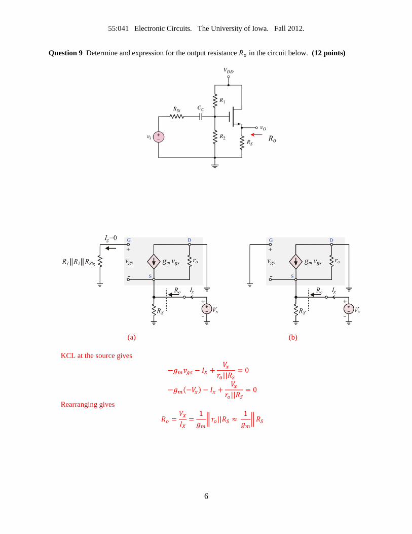
Question 9 Determine and expression for the output resistance in the circuit below. (12 points)
To find , follow the standard procedure: turn off all independent sources ( in this case), add a test
source and determine . Then, ⁄ . The small-signal model for the amplifier is shown in
(a) below. The gate current is zero, so that is zero, and the small-signal model becomes as is
shown in (b). Note that and that is in parallel with .
(a) (b)
KCL at the source gives
( )
Rearranging gives
‖
‖

55:041 Electronic Circuits. The University of Iowa. Fall 2012.
7
Question 10 One can model the two back-to-back diodes in the Wien bridge oscillator below as having
a large-signal resistance RLS for a symmetric voltage excursion. Below is a plot of .
(i) (ii)
(a) Determine the amplitude at which the oscillations stabilize. (10 points)
The gain is
‖( )
The loop stabilizes when 3, that is, when
‖( )
‖( )
This gives as the resistance of the diodes where the loop stabilizes. From the plot
the voltage across the diodes is 0.44 V when . The voltage across is then
( )
The output voltage is 3/2 times this value, or 1.32 V.
(b) Determine the frequency of oscillation (in Hz) of the bridge. (2 points)
( )( )
(c) What is the purpose of the SPICE statement .IC (VA) = 0.01V ? (2 points)
This sets the voltage at node A in the circuit to 0.01 V when the simulation starts. This is required
because there are no ac sources in the circuit. Without the statement the output would be 0 V
indefinitely.

55:041 Electronic Circuits. The University of Iowa. Fall 2012.
8
Question 11 Consider the CE BJT amplifier below.
(a) Draw a small-signal model for the circuit. Include numerical values for and . (6 points)
( ) ⁄⁄
(b) Estimate the upper 3-dB bandwidth of the circuit. (12 points)
The Miller effect transforms to a value ( ) where ( ‖ ), the gain
“ or ing across” . That is
( )( )
The Miller capacitance is in parallel with . A small signal model is
The time constant is ( )( ‖ ‖ ‖ ) ( )( ) . The upper 3 dB
frequency is then ⁄

55:041 Electronic Circuits. The University of Iowa. Fall 2012.
9
Page intentionally left blank

55:041 Electronic Circuits. The University of Iowa. Fall 2012.
10
Question 12 A power MOSFET with o is operating with an averge drain current
of of ̅ , and an average drain-source voltage ̅ . The device is mounted on a heat sink
with paramaters o , and
o . The ambient temperature is
o .
(a) Draw and fully label a thermal model for the problem. (4 points)
The device dissipates ̅ ̅ . A thermal model is shown below.
(b) Determine the temperature of the device (i.e., junction), case, and heat sink. (6 points)
( )
( )
( )
( )
( )
( )
o
55:041 Electronic Circuits. The University of Iowa. Fall 2012.
11
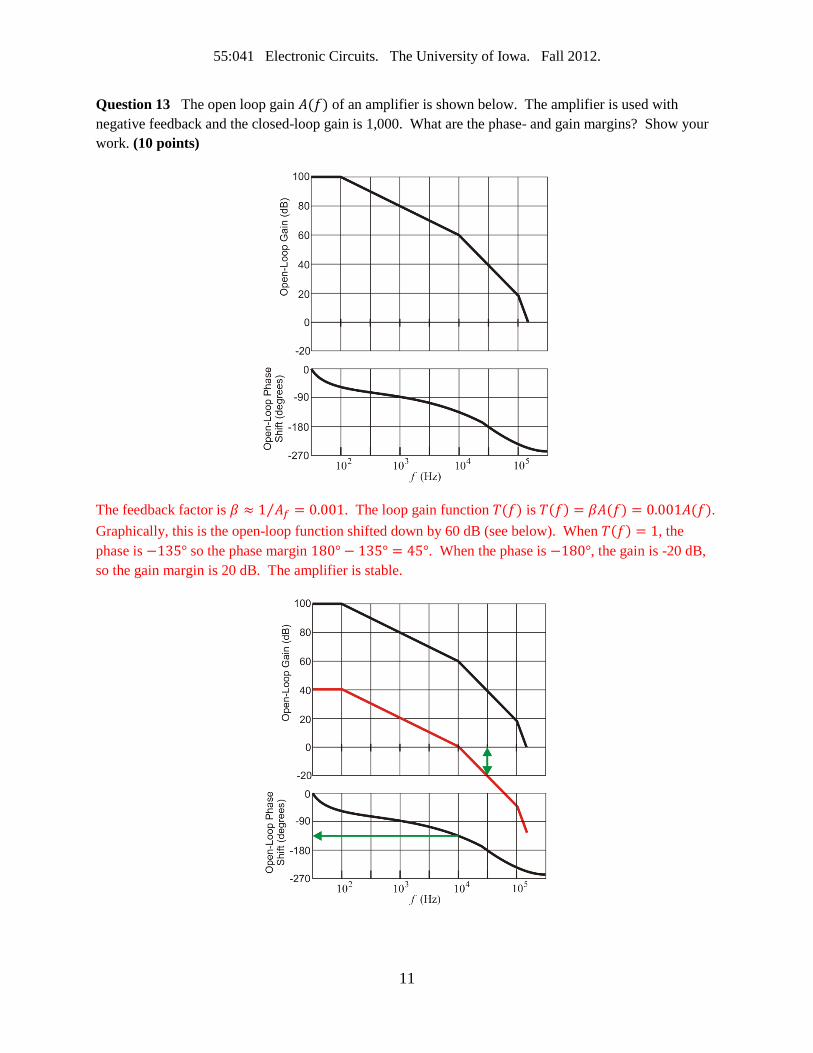
Question 13 The open loop gain ( ) of an amplifier is shown below. The amplifier is used with
negative feedback and the closed-loop gain is 1,000. What are the phase- and gain margins? Show your
work. (10 points)
The feedback factor is ⁄ . The loop gain function ( ) is ( ) ( ) ( ).
Graphically, this is the open-loop function shifted down by 60 dB (see below). When ( ) , the
phase is so the phase margin . When the phase is , the gain is -20 dB,
so the gain margin is 20 dB. The amplifier is stable.

55:041 Electronic Circuits. The University of Iowa. Fall 2012.
12
Question 14 The open-loop gain of an amplifier is modeled by
( )
(
) (
)(
)
An engineer uses the amplifier and negative feedback so that the gain of the feedback amplifier is 560.
(a) What is the feedback factor (4 significant figures). (1 points)
(b) Provide an expression for the loop gain that incorporates ( ) (1 point)
( )
(
)(
) (
)
(c) Find the crossover frequency . That is, the frequency where the magnitude of the loop gain is 1. If
you cannot do this, take for the rest of the problem. (8 points)
( )
√ (
)
√ (
)
√ (
)
Using trail-and-error we find that results in ( ) .
(d) Determine if the amplifier is stable. (6 points)
The phase at is
Substituting shows that . The phase margin is .
The amplifier is stable.