Embed Size (px)
Citation preview

Final Remarks MAM 2016
Volker Saile
February 2, 2016


MAM 2016, 7th Edition
Same Concept, Same Venue, Same Quality
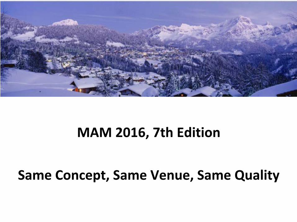
mAm 2010 – the first mAm

mAm 2010

mAm 2012

mAm 2015

mAm 2016

http://villars.roundshot.com/bretaye/
mAm 2016 – the days before in the webcam
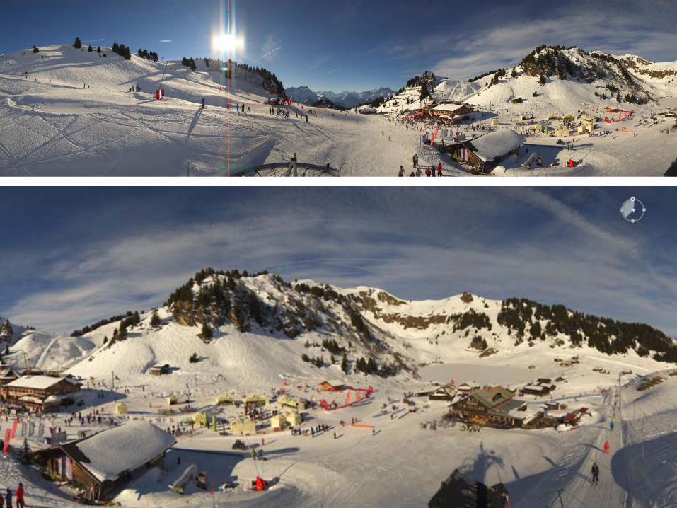

Sunday, January 21, 2016
Its a workshop and not a skiing excursion!


The Concept
mAm
Short Conference/Workshop
Reasonably small Number of Attendees
Highly qualified Attendees
Highly focused Topics
Local Interests
Excellent Venue
…

The Program

Monday 1 February 2016
9:00 - 09:30 Welcome
Danick Bionda, Secretary General, Micronarc
Prof. Dr. Volker Saile, Karlsruhe Institute of Technology, President, Mancef
David Tolfree, Vice President – Europe, Mancef
Christine Reiley, ASME / COMS 2016
Yvan Dénéréaz, Office for Economic Affairs, Canton of Vaud

09:30 - 10:00 Invited Keynote on the Future of Micro-manufacturing I
Chair: Prof. Volker Saile, Mancef; KIT
Prof. Richard Leach, Professor in Metrology, Faculty of Engineering, The University of Nottingham (UK)Next generation optical micro-metrology: beating the current barriers
Why Nottingham?Interests in Micromanufacturing and Additive ManufacturingSurface measurements: spatial frequenciesWhy optical and not contact? Optical instrumentsImaging compromisesInformation rich metrologies (IRM)
Special problem: High slopesDifference Engines
Current research:Develop new all optical CMM platform50 mm³ and sub-µm capabilityFocus and interferometry variationIRM principlesSelf-calibrationIt is never too late to start over!
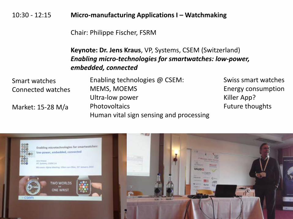
10:30 - 12:15 Micro-manufacturing Applications I – Watchmaking
Chair: Philippe Fischer, FSRM
Keynote: Dr. Jens Kraus, VP, Systems, CSEM (Switzerland)Enabling micro-technologies for smartwatches: low-power, embedded, connected
Smart watchesConnected watches
Market: 15-28 M/a
Enabling technologies @ CSEM:MEMS, MOEMSUltra-low powerPhotovoltaicsHuman vital sign sensing and processing
Swiss smart watchesEnergy consumptionKiller App?Future thoughts

Dr. Rainer Kling, Business Unit Manager / Laser Micromachining, AlphaNov (France)Femtosecond lasers for ultra-precision watchmaking applications
AlphaNov organization
fs-Lasers: advantagesNon-linear absorption
Sapphire: properties
Holes and deep engravingImproving ablation qualityBottom-up ablation
Process window: <2° taper
Laser-drilling strategies: Trepanning drilling, geometry controlHigh AR > 10
Decoration: holographic effects, hydrophobic surfaces, coin making

Dr. Csaba Laurenczy, Haute-École Arc, Lab. d'ingénierie horlogère(Switzerland)Functionality and attribute driven process control and qualityinspection for watch production
Press fittings: up to 80 per watch > production problems
Attribute driven process control: Client needs-functionality of assembly--set of process attributes-assembly functionality check--set of component attributes-component functionality check--client needs

Silvio Dalla Piazza, Vice President Research & Development, Micro Crystal AG [Swatch Group] (Switzerland)Quartz Tuning Forks: A high-volume, low-cost, high-tech MEMS
product
Quartz: Tuning forks = first MEMSToday: miniaturized ceramic packaged quartz resonatorPhotolithography-wet chemical etchingFrequency adjustment by laser trimmingTypes of resonators, 32.768 kHz for watches and smartphonesNew geometry with grooves (Q-factor!)T-compensation and agingSmall: 1.6x1 mm, 2B pieces/a, critical parameter is market price (6 C/ piece !!!)

13:30 - 15:00 Micro-manufacturing Applications II – Medtech
Chair: Pierre-André Grandchamp, FSRM
Keynote: Dr. John T. McDevitt, Chair, Department Biomaterials, New York University College of Dentistry, Bioengineering Institute (USA)Development of the Programmable Bio-Nano-Chip: Bridging theGaps in Micro-Manufacturing for A New Class of Medical Devices
Books, health market, missing link: biomarker information Strategic focus: technical advantage, societal need, passion – flywheel effectSenso DX: Platform to digitize biology, sensor that learns, empower peoplePlatform, barriers, pathway to analyzer, failure of current LOC for POC, New content!Consumer cardiac ScoreCard, adaptive clinical trialsSoft product launch SensoDX in January 2016Internet of Biomarkers (IoB)

Dr. Ben Whiteside, Director – RKT Centre for Polymer MNT, University of Bradford (United Kingdom)Microinjection moulding for microneedle drug delivery devices
RKT Centre for polymer micro- and nano-technology
„Organizing Molecules“
Micro-needles case study
- High shear rheometry- IR shear heating measurements- Design and simulation- Hollow micro-needles- Process analytics
AFM, polymer morphology, analysis techniques, 3D confocal microscopy
Plasma treatment – contact angle

Dr. Vincent Dessenne, General Manager, Heraeus Materials SA (Switzerland)Innovative cermet ceramic composites for miniaturized medicalapplications
Miniature feedthroughs for implants
Example pacemakers: downsizing 1958-2013
Current technology is very complex
CerMet ceramic and conductorNetwork of conductive material (Pt)Absence of macroscopic interfaceStrength, conductivity, leak-tight
Improvement: Polishing, slow cooling
Stacking: 3D designs
Laser welding
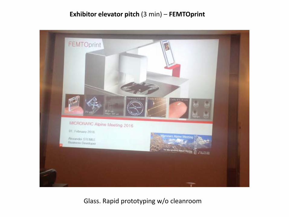
Exhibitor elevator pitch (3 min) – FEMTOprint
Glass. Rapid prototyping w/o cleanroom

15:30 - 17:30 MEMS
Chair: Dr. Sebastian Gautsch, EPFL
Keynote: Benedetto Vigna, Executive Vice President, General Manager, Analog, MEMS & Sensors Group, ST Microelectronics(Italy/Switzerland)Sensors and..... actuators
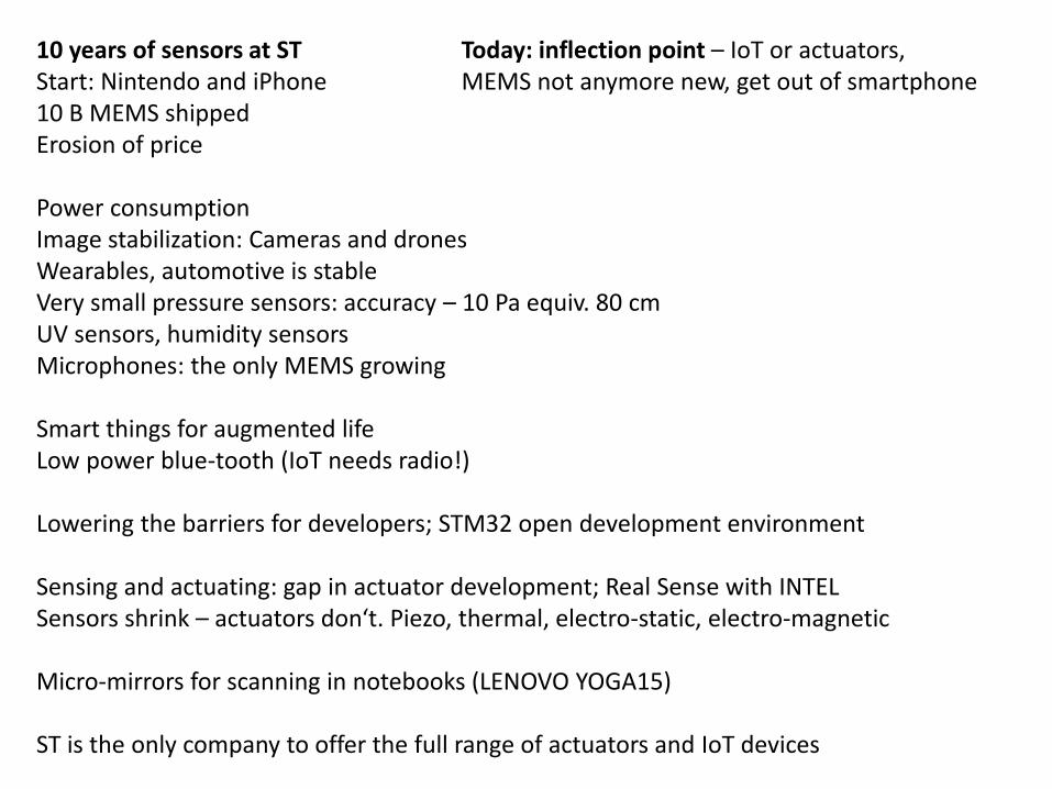
10 years of sensors at STStart: Nintendo and iPhone10 B MEMS shippedErosion of price
Power consumptionImage stabilization: Cameras and drones Wearables, automotive is stable Very small pressure sensors: accuracy – 10 Pa equiv. 80 cmUV sensors, humidity sensorsMicrophones: the only MEMS growing
Smart things for augmented lifeLow power blue-tooth (IoT needs radio!)
Lowering the barriers for developers; STM32 open development environment
Sensing and actuating: gap in actuator development; Real Sense with INTELSensors shrink – actuators don‘t. Piezo, thermal, electro-static, electro-magnetic
Micro-mirrors for scanning in notebooks (LENOVO YOGA15)
ST is the only company to offer the full range of actuators and IoT devices
Today: inflection point – IoT or actuators, MEMS not anymore new, get out of smartphone
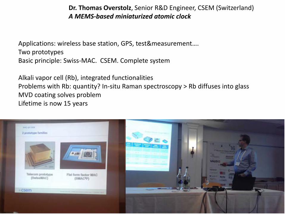
Dr. Thomas Overstolz, Senior R&D Engineer, CSEM (Switzerland) A MEMS-based miniaturized atomic clock
Applications: wireless base station, GPS, test&measurement….Two prototypesBasic principle: Swiss-MAC. CSEM. Complete system
Alkali vapor cell (Rb), integrated functionalitiesProblems with Rb: quantity? In-situ Raman spectroscopy > Rb diffuses into glassMVD coating solves problemLifetime is now 15 years

Dr. Christophe Gorecki, Directeur de Recherche CNRS, Institut FEMTO-ST (France)Miniature Mirau interferometry for swept-source OCT imaging withapplications to cancer diagnosis
Miniature microscopes for auto-diagnosisOptical coherence tomography (OCT)Skin cancer
VIAMOS Consortium – 7 partnersMOEMS based instrumentArchitecture
Demonstrators for building blocksDoublet of 4x4 microlens arraysBeamsplitterZ-scanner
Assembly and characterization

Prof. Dr.-Ing. Helmut F. Schlaak, Technische Universität Darmstadt (Germany)Micro Nano Integration - Iontrack Template Technology for Future MEMS
Nanowires, nanotubes, nanorodsBottom-up fabricationIon-track etchingPrefabricated foils, no expensive equipmentLaminate ion-etched foils, adhesive layerSolvent-enhanced laminationElectroplating
Properties: 100 nm to 1.5 µm, 100µm longElectrical connectionsApplications: many (see photo)
Tayloring of the needles
Upscaling and commercialization

Exhibitor elevator pitch (3 min) – Lyncée Tec
SAW, US-transducer in liquid, EPFL ROLEX Center - Evaporation of the building replica

Excellent!!!

Microtechnologies are fine, but…

…sometimes not the best solution

Tuesday 2 February 2016
08:30-10:00 Novel Manufacturing I - Energy Harvesting
Chair: Dr. Christine Neuy, microTEC Südwest
Keynote: Prof. Adrian Ionescu, EPFL / NANOLAB (Switzerland)Energy harvesting and storage for smart autonomous systems
Wearables and IoTEnergy scavenging: Light, vibration, motionEnergy storage
Nano Era, size of transistors,3D, 14 nm transistors
Trillions of sensors? AbundanceEU Zero-Power technologyAutonomous smart systems
Energy for elementary functions
Wearable technology
Key enabling technologies

Si technology: a 3D migration to the future. Self powered chips?
Solar, thermal, vibration, RF for harvestingMechanisms for energy harvestingMicropower energy harvesting: Solid-State Electronics 53(2009), 684-693
Scenario 1: harvestingScenario 2: harvesting and storage combined
Energy: majority goes into radioScavenging: system level problem
Light: low efficiency at low lux – solutions such as photon recyclingVibrations: mass!Human energy: activities. Where to tap the power? Shoes? Piezoelectric conversion/harvesting: PVDF on wafer, low TThermoelectric (TEG): nanomaterials, performance factors, SEIKO watch, on foil harvester
material, package, systemHot ICs
Storage: Li-ion battery, supercapacitors – advantages/disadvantages, Graphene
Roadmap
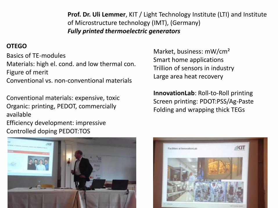
Prof. Dr. Uli Lemmer, KIT / Light Technology Institute (LTI) and Institute of Microstructure technology (IMT), (Germany)Fully printed thermoelectric generators
OTEGO
Basics of TE-modulesMaterials: high el. cond. and low thermal con.Figure of meritConventional vs. non-conventional materials
Market, business: mW/cm²Smart home applicationsTrillion of sensors in industry Large area heat recovery
InnovationLab: Roll-to-Roll printingScreen printing: PDOT:PSS/Ag-PasteFolding and wrapping thick TEGs
Conventional materials: expensive, toxicOrganic: printing, PEDOT, commercially availableEfficiency development: impressiveControlled doping PEDOT:TOS

Dr. Simone Marasso, Chilab, Materials and Microsystems Laboratory, Department of Applied Science and Technology (DISAT), Politecnico di Torino (Italy)3D flexible micro-supercapacitors
Supercapacitors: bursts of energy, low energy densityComparison with batteryTechnological challenges
Graphene based materialMEMSPolymer substrate
Graphene propertiesSolution: graphene oxideThen reduction of GOLoading with metal oxide particlesVery high surface area
Fabrication: LIGA-like, high ARSilicon master3D flexible µsupercapacitorsLoading of µstructureCharacterization 10mF/cm²

Exhibitor elevator pitch (3 min) - IcoFlex
2016: Metrology machine for watchmakers. GyroTracker. Micro-movements of metallic parts

Internet device forecast: mostly wrongBut…smart TV, wearables (?)Smart world – INTELIoT Hypecycle (Gartner 2014)Autonomous cars
IoT applications and sensorsFrom OLED and OPV to SensorsConsumer and industrial applications

Smart homes: will comeBio-degradable electronics (KIT-Forbes, 9-2015)Hybrid wireless sensor node – printing/Si
INNOVATONLab: Printed organic electronicsSensors! Mass production, labels… CHEAP
Printing stages 1, 2 and 3 –Examples: TEGReplace ITO – Touch screen applicationsPrinted force sensor – piezoresistive – medicalLOC printed, diapers-sensors: delivery!Disposable pressure sensor: Decubitus
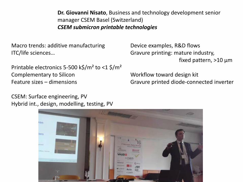
Dr. Giovanni Nisato, Business and technology development senior manager CSEM Basel (Switzerland)CSEM submicron printable technologies
Macro trends: additive manufacturingITC/life sciences…
Printable electronics 5-500 k$/m² to <1 $/m²Complementary to SiliconFeature sizes – dimensions
CSEM: Surface engineering, PVHybrid int., design, modelling, testing, PV
Device examples, R&D flowsGravure printing: mature industry,
fixed pattern, >10 µm
Workflow toward design kitGravure printed diode-connected inverter

Sub-micron: re-tooling from opticsCSEM submicron OTFT building blocksSubmicron OTFT –simulations at CSEM
Gravure 30 microns pitch
USP: value for basic functions
Towards submicron

Dr. Dario Mager, Institute of Microstructure Technology (IMT), KIT, (Germany)Printed MEMS – getting micro manufacturing out of the cleanroom
History of ink jet printing
No cleanrooms, not high volume
Electroplated structures: thin – receiver coilsThickness limited
Self-rolled structures in a tube PDMS µ-tubesDiameters: wide range
µ-NMR receivers: rolling on glass tubeFancy structures inside tubes
Broke man‘s LIGAElectroplate inside trenchPrinted Track used as shadow maskWafer scale
Electrifying Lab on a DiskPrototypesPutting detection and intelligence on diskEnergy supply

Exhibitor elevator pitch (3 min) - microTEC Südwest
380 members – special interest groups: printing, smart health, industry 4.0…

13:30 - 15:00 Novel Manufacturing III - Assembly and Laser Methods
Chair: Danick Bionda, Micronarc
Keynote: Prof. Yves Bellouard, Galatea Lab, Richemont Chair in Micromanufacturing, EPFL (Switzerland)Femtosecond laser processing of dielectrics: a micro-manufacturing platform for single-material multifunctional microsystems
MicrocityOne material – one functionHow about 3-D structures?Increasing number of functionalities
Monolithic integration: example optical bench,one piece of glass, micro-gripperModify material properties locally at will: Non-linear absorption – pulsed lasers

Packaging of optics: positioning by laser
Laser morphing: surface tension (spheres)
Applications with fused Silica
Local increase of refractive indexWaveguides, gratings…
Waveguides+channels, optomechanics, 3D,flexures in glass, waveguides+flexures, Transparent actuators, dielectrophoresisdevices,cantilevers for laser- matter interactions,polarization and stress (Gpa!)
Mechanical properties of glass

Prof. Dr. Klaus-Dieter Lang, Director, Fraunhofer Institute for Reliability and Microintegration IZM (Germany)Advanced Assembly and Integration Technologies for Miniaturized Electronic Systems
Wafer level –panel level integrationSystem integration-driving forcesDesign, Technology, Reliability
Every application requires…
Interface to digital world, human-machine interface
ASTROSE – wireless sensor nodePower line - capacitive harvesterSensor systems and electronicsRequirements on integration
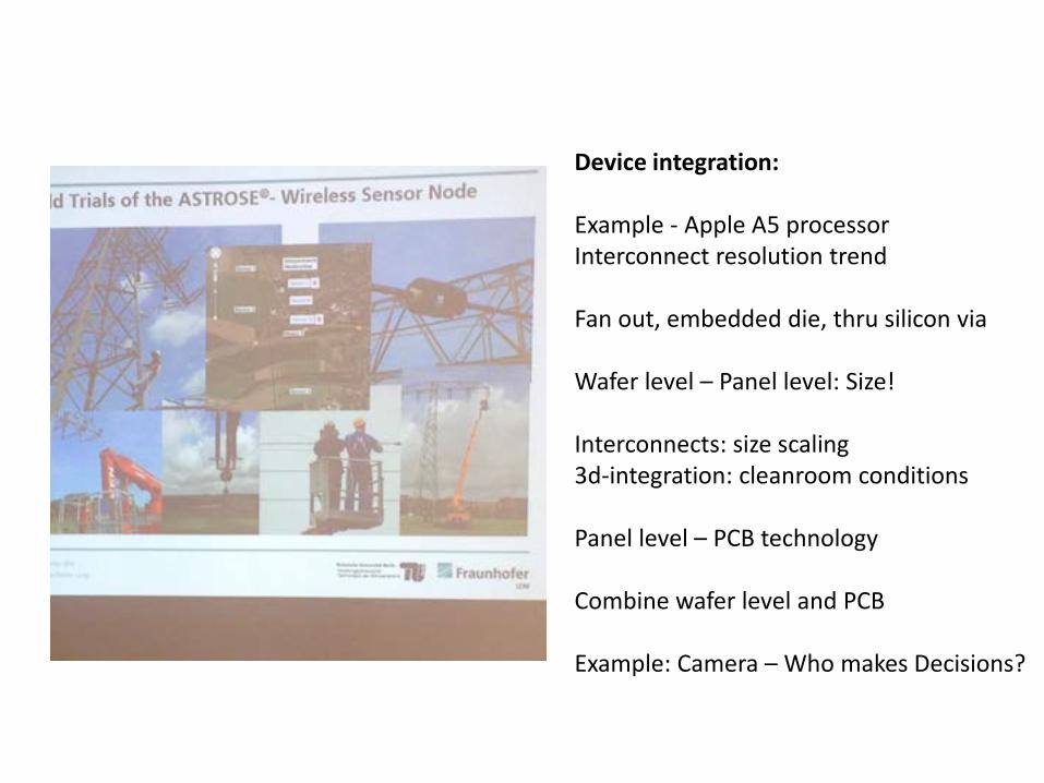
Device integration:
Example - Apple A5 processorInterconnect resolution trend
Fan out, embedded die, thru silicon via
Wafer level – Panel level: Size!
Interconnects: size scaling 3d-integration: cleanroom conditions
Panel level – PCB technology
Combine wafer level and PCB
Example: Camera – Who makes Decisions?

Prof. Dr. Boris N. Chichkov, Leibniz Universität Hannover and Laser Zentrum Hannover e.V. Head of the Nanotechnology Department (Germany)3D laser nanoengineering and printing of nanoparticles
Generation of nanoparticles: Au (ablation)Electrophoretic coatings
Two photon absorptionPhotonic crystals, interconnects, super-strong materialsTissue engineering: scaffolds, also from fibrin3D conductive polymersSplitting of beams
Laser printing of nanoparticles (Au),catch droplets, also as antennae
Huge arrays of nanoparticles
Printing of Si particlesMie theoryAmorphous phase – unstableNon-radiating particlesOptics with nanoparticles

Additive manufacturing:Laser-melting: 100 µm to 1 µmPrint on top on each other AR = 40
Stem cells can be differentiatedwithin the printed pattern

15:30 - 16:15 Invited Keynote on the Future of Micro-manufacturing IIProf. Dr. Andreas Manz, Head of Research, KIST Europe Forschungsgesellschaft mbH (Germany)» European Inventor Award 2015 for lifetime achievementBeyond Microfluidics, biomimetics or self-assembly?
LOC achievementsNo killer apps yet
Early devices3D manifold Older videos
Substrates mostly glass to glassIntegrated features mostly nothing Topology of channelsInterfacing: It is a chip in a labApplication areasCommercializationBest commercial case: CaliperNew horizons?
more of the same?early patents expirednew materials? Paper!new fields? Stem cell biology,organ on a chip, wearablestechnologies? Droplets in oil!Droplets on surface!Large scale int. of valves?Nano scale? Single molecules?

Capillary forces and phase gatesFeed cells by phase gates (MIMETAS company)3d liver cells – metabolism – chip is the bestCanaliculi formation – chip is the best
Microfluidic networks: biological channels:no constant cross section, not smooth
Biomimetic networks: leaf > copy in PDMS > glassMicrofluidics: filling the structureNo straight lines. Put cells into it. Melanoma cells
Self assemblyFlies are self-assembled! Mechanical structures?Si-cubes in paramagnetic fluid and magnetic fieldDiffusion and Brownian motion, combinatorial problemExternally propelled, self propelledMagnetotactic bacteria:Self propelled with external steeringCapillary forces: logic, four parts of self assemblyFabricated SU-8 tripods > Project cancelledSoap bubbles – helices from soap, ion track channels

16:15 - 16:30 Final Remarks
Prof. Dr. Volker Saile, Karlsruhe Institute of Technology (Germany), President, Mancef
Danick Bionda, Secretary General, Micronarc

Thanks
Thanks

See you at COMS2016 in Houston, TX