Embed Size (px)
Citation preview

General rights Copyright and moral rights for the publications made accessible in the public portal are retained by the authors and/or other copyright owners and it is a condition of accessing publications that users recognise and abide by the legal requirements associated with these rights.
Users may download and print one copy of any publication from the public portal for the purpose of private study or research.
You may not further distribute the material or use it for any profit-making activity or commercial gain
You may freely distribute the URL identifying the publication in the public portal If you believe that this document breaches copyright please contact us providing details, and we will remove access to the work immediately and investigate your claim.
Downloaded from orbit.dtu.dk on: Feb 25, 2020
Finite-Difference Frequency-Domain Method in Nanophotonics
Ivinskaya, Aliaksandra
Publication date:2011
Document VersionPublisher's PDF, also known as Version of record
Link back to DTU Orbit
Citation (APA):Ivinskaya, A. (2011). Finite-Difference Frequency-Domain Method in Nanophotonics. Kgs. Lyngby, Denmark:Technical University of Denmark.

Department of Photonics EngineeringTechnical University of Denmark
Finite-Difference Frequency-Domain
Method in Nanophotonics
by
Aliaksandra Ivinskaya
PhD Thesis
2011Lyngby

Thesis submitted in partial fulfillment of the requirementsfor PhD degree in Electronics and Communication
from the Technical University of Denmark
Supervisor:Andrei Lavrinenko
Submitted 20 April 2011
Summary
Optics and photonics are exciting, rapidly developing fields building their suc-cess largely on use of more and more elaborate artificially made, nanostructuredmaterials. To further advance our understanding of light-matter interactions inthese complicated artificial media, numerical modeling is often indispensable.This thesis presents the development of rigorous finite-difference method, a verygeneral tool to solve Maxwell’s equations in arbitrary geometries in three di-mensions, with an emphasis on the frequency-domain formulation. Enhancedperformance of the perfectly matched layers is obtained through free spacesqueezing technique, and nonuniform orthogonal grids are built to greatly im-prove the accuracy of simulations of highly heterogeneous nanostructures. Ex-amples of the use of the finite-difference frequency-domain method in this thesisrange from simulating localized modes in a three-dimensional photonic-crystalmembrane-based cavity, a quasi-one-dimensional nanobeam cavity and arraysof side-coupled nanobeam cavities, to modeling light propagation through metalfilms with single or periodically arranged multiple subwavelength slits.


Resume
Optik og fotonik er spændende og dynamiske forskningsomrader i en rivendeudvikling, der i høj grad baserer sig pa mere og mere komplicerede nanos-trukturerede materialer. Numeriske beregninger er ofte uundvrlige for at øgeforstaelsen af lys-stof vekselvirkning i sadanne kunstige materialer. Denneafhandling præsenterer udviklingen af en rigoristisk finite-difference-metode tilløsning af Maxwells ligninger i vilkarlige geometrier i tre dimensioner medfokus pa frekvensdomæne-formuleringen. Gennem en metode til at pressedet tomme rum opnas en forbedret virkning af perfekt tilpassede lag (Per-fectly Matched Layers), og ikke-uniforme ortogonale net benyttes til at øgenøjagtigheden af beregninger for stærkt heterogene strukturer. Eksemplerpa udregninger med den tre-dimensionelle finite-difference-metode i frekvens-domænet i denne afhandling strækker sig fra lokaliserede tilstande i kaviteteri fotoniske krystal-membraner, kvasi-en-dimensionelle nanobjælke-kaviteter ogrkker af side-koblede nanobjælke-kaviteter til modellering af lysudbredelse gen-nem metalfilm med sprækker der er mindre end bølgelængden.


Preface
This thesis is based upon studies conducted during my stay at the Departmentof Photonics Engineering, Technical University of Denmark, Lyngby, Denmark.Initially I intended to work in quantum optics of nanostructures but my firstencounter with the finite-difference modeling of photonic-crystal cavity hasopened the realm so physically rich and computationally challenging in itselfthat I focused on the finite-difference methods to model photonic band-gap andmetal-based nanostructures.
It is my great pleasure to take this opportunity and thank many people whohelped me with my project — in the first place this is of course Andrei Lavri-nenko, my principle supervisor. I am also grateful to Peter Lodahl and JesperMørk, my co-supervisors at the initial stages of the project. A critical com-ponent for my professional growth was communication with many colleaguesfrom DTU and abroad, in particular Andrei Novitski, Andrei Sukhorukov andDzmitry Shyroki, and the family-like and stimulating atmosphere created inthe Metamaterials group here at DTU-Fotonik. I would also like to acknowl-edge Ulf Peschel (University Erlangen-Nurnberg) for his kind permission to usecomputing facilities of his group to model coupled nanobeam cavities in 2010.
A. IvinskayaLyngby, April 2011


List of publications
Journal papers
P1. D.M. Shyroki, A.M. Ivinskaya & A.V. Lavrinenko, “Free-space squeezingassists perfectly matched layers in simulations on a tight domain,” IEEEAntennas and Wireless Propagation Letters, vol. 9, pp. 389–392, 2010.
P2. A.M. Ivinskaya, D.M. Shyroki & A.V. Lavrinenko, “Modeling of nanopho-tonic resonators with the finite-difference frequency-domain method,” IEEETransactions on Antennas and Propagation, accepted, 2011.
P3. A.M. Ivinskaya, A.V. Lavrinenko, D.M. Shyroki & A.A. Sukhorukov,“Mode tuning and degeneracy in longitudinally coupled nanobeam cavi-ties,” Applied Physics Letters, submitted, 2011.
Conference proceedings
C1. A. Ivinskaya & A.V. Lavrinenko, “Q-factor calculations with the finite-difference time-domain method,” XVI International Workshop OWTNM,Copenhagen, Denmark, PO-01.37, p. 43, 27–28 April, 2007.
C2. A.M. Ivinskaya, A.V. Lavrinenko, A.A. Sukhorukov, D.M. Shyroki, S.Ha & Y. S. Kivshar, “Coupling of cavities: the way to impose control overtheir modes,” Proceedings of SPIE, vol. 7713, pp. 77130F-1–9, 2010.
C3. A.M. Ivinskaya, A.V. Lavrinenko, A.A. Sukhorykov, S. Ha & Y. S. Kivshar,“Longitudinal shift in coupled nanobeams and mode degeneracy,” AIPConference Proceedings, vol. 1291, pp. 121–123, 2010.
C4. A.M. Ivinskaya, D.M. Shyroki & A.V. Lavrinenko, “Three dimensionalfinite-difference frequency-domain method in modeling of photonic nanocav-ities,” 12th International Conference on Transparent Optical Networks IC-TON 2010, Mo.P.16-1–4, Munich, Germany, June 27 – July 1, 2010.


Contents
Summary iii
Resume v
Preface vii
List of publications ix
1 Introduction 11.1 Tailored light-matter interactions: photonic crystals . . . . . . 2
1.1.1 Photonic-crystal-based resonators . . . . . . . . . . . . . 21.1.2 Calculation of Q-factor with finite-difference methods . 6
1.2 Light at nanoscale: metallic nanostructures . . . . . . . . . . . 71.2.1 Phenomenological description of metal . . . . . . . . . . 71.2.2 Nanostructured metals in optics . . . . . . . . . . . . . 9
1.3 Electromagnetics from computational perspective . . . . . . . . 131.3.1 Maxwell’s equations and transformation optics . . . . . 131.3.2 Application to the finite-difference methods . . . . . . . 15
1.4 The aim and outline of this thesis . . . . . . . . . . . . . . . . . 18
2 Finite-difference time-domain method for resonators 212.1 Formulation of the FDTD method . . . . . . . . . . . . . . . . 22
2.1.1 Spatial discretization . . . . . . . . . . . . . . . . . . . . 222.1.2 Time stepping . . . . . . . . . . . . . . . . . . . . . . . 23
2.2 Q-factor evaluation with the FDTD method . . . . . . . . . . . 242.2.1 Excitation of single resonance in the time domain . . . . 242.2.2 Sphere benchmark: field components or energy density? 26
2.3 Transfer to the frequency domain: motivation . . . . . . . . . . 29
3 Finite-difference frequency-domain method 313.1 Two variations . . . . . . . . . . . . . . . . . . . . . . . . . . . 32
3.1.1 Monochromatic wave transmission analysis . . . . . . . 323.1.2 Eigenmode analysis . . . . . . . . . . . . . . . . . . . . 32
3.2 Discretization matters . . . . . . . . . . . . . . . . . . . . . . . 34

xii CONTENTS
3.2.1 Discretization of computational domain interior . . . . . 343.2.2 Boundary conditions and domain reduction . . . . . . . 38
3.3 Modeling of a sphere . . . . . . . . . . . . . . . . . . . . . . . . 423.3.1 Adjusting parameters . . . . . . . . . . . . . . . . . . . 423.3.2 Convergence studies . . . . . . . . . . . . . . . . . . . . 45
4 Ultra-high-Q nanophotonic resonators 494.1 PhC membrane cavity . . . . . . . . . . . . . . . . . . . . . . . 50
4.1.1 Equidistant mesh and arctanh squeezing function . . . . 504.1.2 Non-equidistant mesh and x/(1− x) squeezing . . . . . 52
4.2 Nanobeam cavity . . . . . . . . . . . . . . . . . . . . . . . . . . 564.2.1 2D modeling: high-Q design . . . . . . . . . . . . . . . . 564.2.2 3D modeling . . . . . . . . . . . . . . . . . . . . . . . . 61
5 Coupled nanobeam cavities 655.1 Two coupled nanobeams . . . . . . . . . . . . . . . . . . . . . . 66
5.1.1 2D analysis of field profiles . . . . . . . . . . . . . . . . 665.1.2 3D Q and λ dependence on the longitudinal shift . . . . 71
5.2 Three coupled nanobeams . . . . . . . . . . . . . . . . . . . . . 755.2.1 Weak coupling regime . . . . . . . . . . . . . . . . . . . 755.2.2 Strong coupling regime . . . . . . . . . . . . . . . . . . 77
6 Metallic gratings 816.1 Planar metallic slab at THz frequencies . . . . . . . . . . . . . 82
6.1.1 Analytic solution . . . . . . . . . . . . . . . . . . . . . . 826.1.2 FDFD testing . . . . . . . . . . . . . . . . . . . . . . . . 84
6.2 Single slit . . . . . . . . . . . . . . . . . . . . . . . . . . . . . . 846.2.1 1/f law for enhancement . . . . . . . . . . . . . . . . . 866.2.2 Enhancement dependence on the slit width . . . . . . . 87
6.3 Periodic slits in metal film . . . . . . . . . . . . . . . . . . . . . 886.3.1 10-nm-wide slit in gratings of different periods . . . . . 906.3.2 Changing slit width when the period is fixed . . . . . . 96
7 Conclusion 99
Appendix A Fourier transformation 101A.1 Continuous Fourier transformation . . . . . . . . . . . . . . . . 101A.2 Discrete Fourier transformation . . . . . . . . . . . . . . . . . . 102
Appendix B Fabry-Perot resonator: FEM versus FDFD perfor-mance 103
Bibliography 105

Chapter 1
Introduction
Just half a century ago manipulating light at the micro- and nanoscale washardly possible or even imaginable. By now progress in fabrication techniquesand our understanding of light-matter interactions have turned optics into oneof the most dynamic, rapidly developing and promising fields of mesoscopicphysics; even the new term, photonics, was invented and widely accepted toemphasize numerous new developments and directions such as image resolutionbelow diffraction limit [1–4] and superfocusing [5–7]; optical cloaking [8–11]; ul-trafast photonic chips [12–16]; lossless, nonlinear and gain materials [17–19]; op-tical modulators [20,21], couplers [22,23], switches [24,25] and light sources onnanoscale [26–29]. This is naturally followed by a multitude of applications totechnology [30], biophysics [31,32], energy harvesting [33–35], lightning [36,37],and medical science [38–40]. And like fifty years ago it was hard to envisagethe perspectives of semiconductor transistor in building computers and all ofthat today’s electronic equipment, it is in the same way unpredictable whatcurrent research activity in nanophotonics will lead to. What we can say withconfidence yet is that in order to utilize the tremendous potential of classicaland quantum optics phenomena in real-life applications, a systematic under-standing and deep intuition for the behavior of light in various nanostructuredarrangements should be developed by each practitioner in the field.
To develop such intuition for light-matter interactions in complex photonicbandgap or plasmonic structures, to design nontrivial devices and to explorenew phenomena, efficient numerical modeling is the key. For an impression oftypical basic problems faced in nanophotonics and computational electromag-netics today, we describe in the following introductory sections two examples:light trapping in photonic-crystal cavities and propagation through metal grat-ings. Then we formulate equations to be solved and sketch the ways we followto do that cleverly, using the same ideas that underpin the recent rise of trans-formation optics. Formulating the aim and outline of this thesis closes theintroduction.

2 Introduction
1.1 Tailored light-matter interactions: photoniccrystals
1.1.1 Photonic-crystal-based resonators
In the coming decade in physics great effort will probably be devoted, amongother things, to improving quantum storage and teleportation, and the devel-opment of quantum computer. This would require increased level of controlover quantum behavior of light. In experiments, quantum states are easilydestroyed by decoherence induced by surroundings. To make use of quantumprocesses one should avoid this influence, or use specifically designed environ-ment to modify the process considered. This is the case when an atom ora quantum dot — nanosized emitter in active material — is located inside amedium exhibiting modified density of electromagnetic states, i.e., a photoniccrystal.
As a popular definition goes, photonic crystal is a structured medium thatcan block light within a range of frequencies called photonic band gap [41].Main advantages of dielectric photonic crystal components over, for instance,their plasmonic analogues are low-loss operation and low-cost production. Pho-tonic crystal based structures — beam splitters, cavities, slow light and logicdevices — allow for a lot of diverse operations with light. Fundamental char-acteristic of photonic crystal that regulates quantum dot spontaneous emissionlifetime is the local density of states, i.e. density of electromagnetic modes ina particular point in the structure. Changing photonic crystal geometry andquantum dot position placed inside the crystal can dramatically alter sponta-neous emission rate. In fact, prospects to modify the density of states gavemajor motivation to investigate photonic crystals back in the years of theirinception, and still they generate large interest from the fundamental cavityquantum electrodynamics perspectives [42–44].
A defect in photonic crystal gives rise to new modes with discrete frequenciesinside the band gap and acts as a cavity capable of trapping radiation due tomultiple reflections from the rest of the photonic crystal. A quality factor of acavity mode is defined as 2π times the ratio of the cycle-averaged total energyof the cavity to the energy loss per cycle [45–47]:
Q = 2π1T
∫T
∫Vw d3rdt
−∫T
∫V
∂w∂t d3rdt
(1.1)
where w = 14 (E · D∗ + B · H∗) is the period-averaged energy density of elec-
tromagnetic field, V the volume of the cavity, T the period of field oscillations,and minus in the denominator corresponds to the energy loss. Assume theenergy density decays exponentially,
w(r, t) = w0(r)e−ω0t
ξ (1.2)

1.1 Tailored light-matter interactions: photonic crystals 3
where ω0 is the angular frequency of electromagnetic wave. Substituting thisto Eq. (1.1) gives ξ = Q. This solution does not depend on which part ofthe cavity, V , we use to calculate the Q-factor. The electromagnetic fieldcomponents of a single cavity mode are given by the usual solution of Maxwell’sequations, the harmonic wave of frequency ω0 with the exponential multiplierstanding for the losses:
A(r, t) = A(r)e−ω0t2Q e−iω0t (1.3)
Formula (1.3) is valid only for one mode being excited, when the field evolu-tion can be described as single-exponential. Squared absolute value of Fourierdecomposition of exponentially decaying harmonic signal, |A(r, ω)|2, gives apackage of monochromatic waves spread near the resonance frequency ω0 withthe half-width δω = ω0
Q as shown in Appendix 1. Thus the Q-factor can be
defined from |A(ω)|2 averaged over the area,
Q =ω0
∆ω. (1.4)
When we deal with a high-Q cavity, energy decays very slowly in it and onlypart of the total decay time is used for FFT. Frequency spectrum fitting tolorentzian is commonly done to reconstruct discretized signal correctly.
The dissipation of power described by the denominator of (1.1) can berewritten in a more convenient way with use of the conservation law∫
V
∂w
∂tdv = −
∮Γ
S · n ds (1.5)
where S = 12E × H∗ is the Poynting vector, Γ is the surface surrounding the
volume V and having the unit normal vector n. So the quality factor is
Q =ω0
∫T
∫Vw d3rdt∫
T
∮ΓS · nd2rdt
. (1.6)
For cavities formed by objects with dimensions comparable with the wave-length of light it is often difficult to define precise physical dimensions of thecavity, and it is possible only when the mode is excited. Indeed, resonance phe-nomena in nanoscale structures are often characterized by very intensive fieldsbehind the borders of the objects formally shaping the resonator by itself. As ameasure of light localization in the cavity it is convenient to use mode volumedefined in quantum mechanics as
V =
∫ϵ(r)|E(r)|2 d3r
max[ϵ(r)|E(r)|2](1.7)
where ϵ(r) is the dielectric permittivity and E(r) the electric field, the integra-tion assumed to be carried out trough the whole space. In the finite-difference

4 Introduction
implementation the integral is replaced by summation over the computationaldomain.
Photonic crystals (PhC’s) are currently considered as a perspective platformto host low mode volume cavities with high quality factors. A defect can beformed in a photonic crystal by breaking a perfect symmetry of the structureeither by removing or shifting basic constitutive units or by local modificationof refractive index. The defect acts as a cavity capable of storing energy duringtime proportional to the Q-factor. For a quantum dot placed inside a defect in aphotonic crystal as in Fig. 1.1a, the radiation rate is directly connected with thequality factor of the microresonator. This gives an explicit way to enhance thequantum dot radiative lifetime by increasing the Q-factor. Another importantparameter is mode volume V . Radiative emission lifetime of an ideal emitterplaced inside a cavity is given via Purcell’s factor [48]:
Fp =3Q(λ/n)3
4π2V. (1.8)
Photonic-crystal-based cavities exhibit very high ratios Q/V [49, 50] andthus they are attractive for use as passive optical components in the rapidlydeveloping area of cavity quantum electrodynamics [51,52]. Astonishing quan-tum phenomena are possible to observe with this kind of cavities, such asthe enhancement of luminescence, alternation of emitter lifetime, Rabi oscil-lations, single-photon emission, and the enhancement of slow down factor inelectromagnetically induced transparency. A variety of high-Q, low-V cavitydesigns were proposed based on structural modifications in photonic crystalmatrices [53–56]. Basically, for a photonic crystal featuring full 3D band gap, adefect in it should give the Q-factor approaching infinity, i.e., light can be keptinside the resonator infinitely long. However, fabrication of photonic crystalswith full 3D band gap, e.g., inverted opals and woodpile structures and defectsin them is quite complicated.
That is why a standard way to create a cavity is to use 2D photonic crystalplatform, mostly silicon or GaAs slabs with perforation. Position of holes in aslab is manually defined, giving thus flexibility in the design and optimization ofcavities and other photonic components. The main channel for loosing radiationfrom a free-standing membrane cavity is through coupling to radiative modes.In the plane of the slab photonic crystal acts as a distributed mirror stronglyholding radiation, thus in-plane leakage of radiation from photonic crystal istypically small. By separating the energy flow into in-plane (||) and out-of-plane (⊥) parts, we can write [57]:
1
Q=
1
Q||+
1
Q⊥, (1.9)
where Q is the total Q-factor, Q|| quantifies losses only in the plane of the slab,while Q⊥ stands for the out-of-plane losses. Knowing that Q|| is very large weimmediately see that the total Q-factor is mainly governed by Q⊥. In the out-of-plane direction light is primarily confined by total internal reflection, thus

1.1 Tailored light-matter interactions: photonic crystals 5
(a) (b)
Figure 1.1: (a) Two coupled identical nanobeam cavities. (b) Even mode incoupled nanobeams.
the magnitude of k⊥ vector should be as small as possible to reduce losses.In-plane mirror imperfections and parasitic leakage by coupling of the cavityradiation to vacuum modes are not clearly separated one from another andcan be closely connected for some modes. Distribution of k|| for a specificmode can be obtained through spatial Fourier transformation of a given modefield component. The usual approach employed for optimization of cavities isthrough some guess for the design that would give k||-vectors mostly lying farenough from the light cone.
Thus if some modes are to be confined at the nanoscale to achieve highQ, this should be done gently without abrupt changes in the structure geom-etry or refraction index because otherwise undesirable leakage will appear. Inthis sense the best designs are given by utilizing the mode-matching rule [58]when the holes pattern changes gradually going from the cavity center towardsthe mirror part. Waveguide-like [59] and nanobeam cavities [60] having simplearrangement of field maxima and minima along a straight line allow applica-tion of such mode matching approach and actually they give the highest ofreported Q-factors. For modes of more complicated symmetries, for instance,for the hexapole mode in a one-hole-missing membrane [61], this approach isnot readily applicable since the mode by itself can be easily destroyed andit disappears completely by a moderate geometry modification, especially ifsymmetry breaks even slightly.
Nanobeam cavity designed by mode-matching approach gains intensive in-terest [62]. It exhibits a set of highly desirable characteristics: high modequality factor Q, low mode volume V (less than the cubic wavelength of light)and the smallest footprint size among other high-Q cavities; this stimulatesintensive investigations of nanobeam-related acousto-optic and optomechanicinteractions [63, 64]. Tiny size of nanobeam cavities makes them also verypromising for densely integrated photonic circuits.
One of the challenging tasks in cavity design remains the shaping of thefar field radiated from the cavity to form a spot, which is necessary if this

6 Introduction
cavity is to be used to make a laser. High-intensity emission to the far fieldis achieved by perturbing cavity design in order to create significant couplingto radiation modes. Recently periodic modification of hole radii in the mirrorpart was proposed as a stable way to extract radiation from the cavity [65].Unfortunately, such solutions completely destroy high Q-factor desirable forlasing; a special design where all leakage of radiation goes into a single spacechannel is highly needed. Although active research is being carried out inthis direction [66–69] the question whether it is possible to create a 2D-basedphotonic crystal cavity which simultaneously has high Q and is capable ofhighly collimated emission along specified direction is waiting for an answer.
Of particular interest are ensembles of cavities [70] with quantum dotsplaced inside, Fig. 1.1a. Three-dimensional description of such systems is notyet a routine task, but it is very important for fundamental investigations oflight-matter interactions [71–73]. Coupling between resonators is an impor-tant feature that allows to shift operation wavelengths. Figure 1.1b showsone of the super-modes showing up when two cavities are brought together.This ‘even’ mode has the wavelength significantly different from a single-cavityeigenwavelength. Several cavities in close proximity to each other cannot beconsidered independently: their interaction should be taken into account as itcan alter substantially the operation of these cavities on a densely integratedchip. Avoiding of parasitic coupling is crucial for photonic integrated circuitsand in optic network design. On the other hand, there are many applicationswhere strong and controllable coupling [74] is required: for example, in orderto create low-threshold lasers [75], to observe Fano line shapes [76], to de-sign field concentrators for detection of molecules [77], to create flat passbandfor slow light [78, 79], holographic storage [80], nonlinearities [81]. Formally,consideration of coupled cavities is directly paralleled with mode hybridiza-tion in molecules, that is why coupled resonators are often called ‘photonicmolecules’ [82, 83].
1.1.2 Calculation of Q-factor with finite-difference meth-ods
Investigation of light behavior in photonic crystals of finite size in two or threedimension relies heavily on numerical computation methods. In fact, direct nu-merical methods attained rapid development in line with rise of nanophotonicsand in particular with the development of the concept of photonic crystal.Multi-surface photonic crystal structures are difficult to describe even approx-imately using analytical considerations. One of the most challenging computa-tional tasks is evaluation of the Q-factor of a resonator. High Q implies large,multi-period-extended photonic mirror capable of holding radiation for a longtime avoiding the losses through coupling to radiative leaky modes. Traditionalway here is to use time-domain modeling to simulate these spatially extendedstructures, with the subsequent extraction of Q by analyzing the ring-downof electromagnetic field components; such simulations can take considerable

1.2 Light at nanoscale: metallic nanostructures 7
time up to several days per single run for high-Q three-dimensional resonator.Of course, for this type of problem we even do not mention the possibility ofthorough convergence studies; only a few papers report such investigations [84].Many approaches are suggested to minimize time consumption of Q-factor eval-uation by transient analysis [85,86] but systematic comparative studies of thesevarious approaches are still lacking and this complicates the choice of a suitableone for a particular resonator considered.
Transition to the frequency domain analysis for cavity eigenmodes is verynatural; it greatly reduces computation time and no post-processing is neededto determine the Q-factor. At the same time reliable frequency-domain solversto find the Q-factor of a resonator are scarcely reported, probably becauseof large memory consumption inherent to many algorithms for computing theeigenvalues of the finite-difference matrix. This work is intended partly to ad-dress this issue by showing that the finite-difference frequency-domain (FDFD)method is capable of calculating high Q factors of membrane resonators evenon a personal laptop if special care is paid to the physical issues of problemset-up, such as solution-adapted continuous grid density variation (of lower res-olution in photonic crystal mirror part, for example; see Fig. 1.1b where thefield decays rapidly from the nanobeam cavity center), exploiting the symme-tries of a resonator to reduce computational domain, and squeezing the freespace around a membrane.
1.2 Light at nanoscale: metallic nanostructures
1.2.1 Phenomenological description of metal
For metals containing free electrons of density ρ the expression for ‘effective’ ϵcan be constructed with use of relation for current J generated by these freeelectrons when external electric field is applied:
J = σE, (1.10)
σ being the conductivity of metal. Supposing time-harmonic excitation suchthat ∂t → −iω, we can write:
J =∂P
∂t= −iωP (1.11)
Combining (1.10) and (1.11) gives
P = iσ
ωE (1.12)
so that the effective permittivity of metal in this model can be introduced is
ϵ∗ = ϵ+ iσ
ϵ0ω(1.13)
8 Introduction
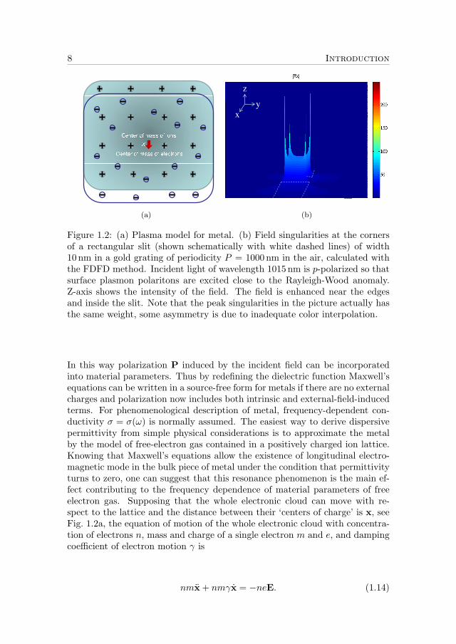
(a) (b)
Figure 1.2: (a) Plasma model for metal. (b) Field singularities at the cornersof a rectangular slit (shown schematically with white dashed lines) of width10 nm in a gold grating of periodicity P = 1000 nm in the air, calculated withthe FDFD method. Incident light of wavelength 1015 nm is p-polarized so thatsurface plasmon polaritons are excited close to the Rayleigh-Wood anomaly.Z-axis shows the intensity of the field. The field is enhanced near the edgesand inside the slit. Note that the peak singularities in the picture actually hasthe same weight, some asymmetry is due to inadequate color interpolation.
In this way polarization P induced by the incident field can be incorporatedinto material parameters. Thus by redefining the dielectric function Maxwell’sequations can be written in a source-free form for metals if there are no externalcharges and polarization now includes both intrinsic and external-field-inducedterms. For phenomenological description of metal, frequency-dependent con-ductivity σ = σ(ω) is normally assumed. The easiest way to derive dispersivepermittivity from simple physical considerations is to approximate the metalby the model of free-electron gas contained in a positively charged ion lattice.Knowing that Maxwell’s equations allow the existence of longitudinal electro-magnetic mode in the bulk piece of metal under the condition that permittivityturns to zero, one can suggest that this resonance phenomenon is the main ef-fect contributing to the frequency dependence of material parameters of freeelectron gas. Supposing that the whole electronic cloud can move with re-spect to the lattice and the distance between their ‘centers of charge’ is x, seeFig. 1.2a, the equation of motion of the whole electronic cloud with concentra-tion of electrons n, mass and charge of a single electron m and e, and dampingcoefficient of electron motion γ is
nmx+ nmγx = −neE. (1.14)

1.2 Light at nanoscale: metallic nanostructures 9
For harmonic electromagnetic field E(t) = E0 exp(−iωt) this gives the displace-ment law and hence the polarization as
P = −nex = − ne2
m(ω2 + iγω)E (1.15)
Inserting this into the expression for electric displacement vector we arrive atthe Drude model for metal permittivity:
ϵ = ϵ∞ −ω2p
ω(ω + iγ)(1.16)
Here ωp = ne2
ϵ0mis plasma frequency at which in the lossless model (γ = 0)
electronic gas suspended in the air (ϵ∞ = 1) responds to incident radiationby excitation of a bulk plasmon, so that ϵ = 0. In general the term ϵ∞ canalso be frequency-dependent and then additional terms described by Lorentzianfunctions appear to take into account the interband transitions. In this thesiswe will mostly deal with pure noble metals at low frequencies that are very welldescribed by simple Drude model, but one should remember that with the sameeasiness arbitrary dispersion can actually be handled by the frequency-domainmethod.
1.2.2 Nanostructured metals in optics
Metal-containing nanostructures exhibit amazing physical phenomena due toinherent property of metal to react to electromagnetic radiation through theinduction of electron currents which are bound within metallic parts of thenanostructure. This can significantly change the properties of the system underthe condition of resonance excitation. Electromagnetic cloaking, resolution un-der diffraction limit, negative refraction, extremely high local density of statesare only part of the most cited phenomena obtained with the use of metal-containing structures. The most amazing feature of interaction of light withmetals is the existence of plasmon polaritons — coupled resonance excitationsof light and electrons close to the metal surface. Two main types of resonance-like effects are possible to observe in metallic structures [87]: resonances origi-nating mainly from the geometry of the structure like Fabry-Perot conditionsor Rayleigh-Wood anomalies (Fig. 1.3) and resonances by matching conditionsbetween permittivity function of the metal and of the host matrix like Mieresonances, i.e. localized plasmons or propagating surface plasmon polaritons.Of course, for many realistic complicated structures it is difficult and some-times not possible to distinguish between the two mechanisms as both of themsimultaneously contribute to the process of light transmission and scattering,and geometrical parameters of the structure regulates contribution from eachof the mechanisms. For instance, although Fabry-Perot and Rayleigh-Woodphenomena show up in dielectric structures, in metals their appearance is alsoassociated usually with excitation of surface plasmons [88–90]. Of course, here

10 Introduction
0.2 0.4 0.6 0.8 1 1.2 1.4 1.6 1.8 2
x 104
0
0.002
0.004
0.006
0.008
0.01
λ, nm
T
P = 5⋅104 nmw = 10 nmh = 20 nm
Figure 1.3: Transmission spectrum of the gold grating of period P , thickness hand width of the air opening w under illumination by p-polarized light, calcu-lated with the FDFD method. Note that the gold behaves very much like thePEC in this wavelength range, and the Rayleigh-Wood resonances are quiteaccurately given by the rule P/n, where n is positive integer.
we are discussing Fabry-Perot ‘nanoscale’ resonances, e.g. those appearing instructures having one of the dimensions with size on the order of one wavelengthor less. For example, slits in metal films of height h can give resonances at con-dition kh+ ϕ = π where ϕ is the phase of reflection and k is the wave numberof whatever mode is propagating back and forth inside the slit, and could, e.g.,be the wave number of a gap plasmon polariton as in Ref. [90]. Because of thereflection phase in the resonance condition, Fabry-Perot transmission peaks areobserved even for thin films [90].
Localized plasmons
Physical explanation of the existence of localized plasmons is that at certainconditions the electrons in metal behave like plasma. For a bulk piece ofmetal, plasma-like behavior occurs at ϵmetal = 0 when the longitudinal solutionof Maxwell’s equations exists and leads to the emergence of bulk plasmons,whereas for small pieces of metals, for example small spheres, this transfersto condition of zero denominators in the Mie scattering coefficients giving theFrohlich condition [91]:
Re(ϵmetal(ω)) = −2 ϵhost (1.17)

1.2 Light at nanoscale: metallic nanostructures 11
where ϵmetal stands for the metal permittivity and ϵhost for the dielectric func-tion of the host medium.
More than a hundred of years from the discovery of Mie, his analytic theoryfor light scattering and transmission by a spherical particle is a reference pointin various fields of research. Nowadays metal nanoobjects get much attentionin photovoltaics due to high absorption at resonance [92], while closely placednanoparticles arranged in special manner can lead to unique features like extra-high field enhancements and negative refraction due to magnetic resonances.
To describe the ensemble of nanoparticles, multiple scattering theories areusually employed where single scattering event is described in the quasi-staticapproximation [93]. In this approximation only the first order dipole mode isconsidered in Mie theory decomposition. When separate particles are smalland their dilution is of low concentration the quasi-static approximation worksperfectly, but for higher concentrations this approximation fails. The reasonfor this is unusual response of nanoobjects under illumination by evanescentwaves, large amount of which is present in the near field of a resonating spherefor example. It was shown that evanescent radiation incident upon a simplesphere can efficiently excite higher order electric and magnetic multipoles [94]which leads to their scattering cross section many times enhanced comparedto plane wave excitation and thus higher-order terms in Mie decompositioncannot be neglected. In a densely packed ensemble of particles they shine oneach other not only by transversal scattered waves but also by evanescent waves,so analytical multiple-scattering theories cannot describe correctly all spectralfeatures of the sample. Thus direct numerical methods to solve Maxwell’sequations need to be employed in the case of aggregates of spherical resonators,although rigorous analytic solution is available for each single sphere.
Surface plasmon polaritons
We consider localized plasmons which are resonant excitations of metal nano-objects, i.e. standing wave pattern is formed inside plasmon nanoparticles andthese standing waves do not transfer energy. At metal-dielectric interface it ispossible to excite surface plasmon polariton (SPP) that can propagate along theplane separating the two media. In the direction perpendicular to the surface,SPP has exponentially decaying tails. Dispersion relation for SPP propagatingat the interface between two half-spaces is:
kspp = k0
√ϵ1ϵ2
ϵ1 + ϵ2(1.18)
Here kspp is the propagation constant of SPP, k0 is the wave vector in vacuum,ϵ1 and ϵ2 are permittivities of metal and dielectric. Thus in contrast to localizedplasmons, propagating SPPs can exist in wide range of frequencies. SPPs arelaunched by evanescent coupling through a waveguide or a prism, or anotheroption is to introduce a corrugation to the flat surface, see Fig. 1.2 displayingstrong diffraction of light near sharp metallic edges. It was suggested that
12 Introduction
0
500
1000
1500
2000−400 −300 −200 −100 0 100 200 300 400
S/|S|y,
nm
x, nm
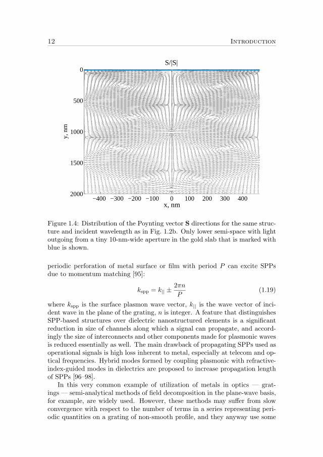
Figure 1.4: Distribution of the Poynting vector S directions for the same struc-ture and incident wavelength as in Fig. 1.2b. Only lower semi-space with lightoutgoing from a tiny 10-nm-wide aperture in the gold slab that is marked withblue is shown.
periodic perforation of metal surface or film with period P can excite SPPsdue to momentum matching [95]:
kspp = k|| ±2πn
P(1.19)
where kspp is the surface plasmon wave vector, k|| is the wave vector of inci-dent wave in the plane of the grating, n is integer. A feature that distinguishesSPP-based structures over dielectric nanostructured elements is a significantreduction in size of channels along which a signal can propagate, and accord-ingly the size of interconnects and other components made for plasmonic wavesis reduced essentially as well. The main drawback of propagating SPPs used asoperational signals is high loss inherent to metal, especially at telecom and op-tical frequencies. Hybrid modes formed by coupling plasmonic with refractive-index-guided modes in dielectrics are proposed to increase propagation lengthof SPPs [96–98].
In this very common example of utilization of metals in optics — grat-ings — semi-analytical methods of field decomposition in the plane-wave basis,for example, are widely used. However, these methods may suffer from slowconvergence with respect to the number of terms in a series representing peri-odic quantities on a grating of non-smooth profile, and they anyway use some

1.3 Electromagnetics from computational perspective 13
absorbing boundary conditions similar to those used in real-space methods; of-ten, real-space numerical simulation has to be performed to confirm the resultsof these semi-analytical mode decomposition approaches [99].
Figure 1.2b shows how well the field singularities can be described if non-uniform mesh is introduced to better resolve high-intensive fields near the metaledges. Evanescent waves close to these hot spots in metals are very intensiveand can spread far enough in space, so the computational domain should beextended accordingly to let these evanescent tails decay sufficiently. This isnot the only reason why metallic structures require thick air buffer: see theenergy flow behind metal grating illuminated with p-polarized light in Fig. 1.4which is characteristic also for off-resonance condition [100, 101]. To calculatetransmission by grating correctly, at least some field vortices should fall insidethe computational domain — otherwise numerical accuracy degrades very fast.This motivates the application of free-space squeezing for metallic structuresno matter whether the structure is on or off resonance.
By now we have discussed two examples: aggregates of metallic spheres andgratings, where application of some analytic considerations is possible. It wasshown [99] that these semi-analytical approaches sometimes cannot catch allthe features inherent to metal-dielectric structures and some help from directbrute force methods is required. A huge variety of plasmonic structures, inparticular those emerging within new fascinating directions in optics such asinvisibility or negative refraction, have such complicated shapes that it wouldnot be possible to explore them at a sufficient level at all if not the usage ofdirect numerical methods.
1.3 Electromagnetics from computational per-spective
1.3.1 Maxwell’s equations and transformation optics
The equations that are known for more than a century and still form the basisfor much of the current progress in nanophotonics are Maxwell’s equations:
∇×E = −∂tB, ∇ ·B = 0 (1.20a)
∇×H = ∂tD+ J, ∇ ·D = ρ (1.20b)
where E and B are the electric and magnetic ‘force vectors’ while D and Hare the electric and magnetic ‘flux vectors,’ ρ and J denote charge and currentdensities. The richness of solutions to Maxwell’s equations owes itself to a greatvariety of natural and artificial materials and structure geometries giving riseto various forms of the constitutive relations between excitation fields E, Band inductions D, H; in many cases they can be written as simply as
D = ϵ0E+P = ϵ0ϵE (1.21a)
B = µ0µH. (1.21b)

14 Introduction
Figure 1.5: Covariance of Maxwell’s equations applied to optimize devices inoptics and for creation of non-uniform meshes in computational electromagnet-ics. (a) and (b) are after [102].
Here ϵ0 and µ0 are the electric permittivity and magnetic permeability ofvacuum, ϵ is the relative permittivity of medium considered. The intrinsicmedium polarization P is related to the electric field through the susceptibilityχ, P = ϵ0χE, and the relative permittivity is thus ϵ = 1 + χ.
A great deal of activity in optics in the last years exploits the transfor-mation invariance of Maxwell’s equations, i.e., the property to look the samein different coordinate systems [103]; even a specific term, transformation op-tics [11,104,105], was coined to represent this new fascinating area of research.When going from one coordinate frame to another linked according to a differ-entiable law, all the transformation properties are enclosed in the permittivity,permeability and electric and magnetic field transformation laws while the formof Maxwell’s equations preserves unchanged. The x to x′ mapping (spanningover all coordinates is supposed here) gives the jacobian
[J ] =∂x′
∂x= [J(x′)], (1.22)

1.3 Electromagnetics from computational perspective 15
and material parameters in the primed system are:
[ϵ′] = |det J |−1[J ] [ϵ] [J ]T (1.23a)
[µ′] = |det J |−1[J ] [µ] [J ]T (1.23b)
Here we suppose that knowing the analytical dependence x = x(x′) materialproperties can be redefined in primed system, for example, dielectric functionis written as ϵ → ϵ(x(x′)) = ϵ(x′). The form of transformation rules for electricand magnetic fields is one and the same: if for simplicity the field is denotedas F, in the primed space it will take the value
F′ = [J−1] F (1.24)
This formula means that, for example, when a new, primed system is threetimes ‘stretched’ in one direction, x′
i = 3xi and hence J = J i′
i = 3, thefield components pointing along the ith direction are three times ‘stretched’in the x′ coordinate frame. This opens a new way to manipulate fields througha fairly simple mathematical tool. The field can be easily stretched [106],squeezed [102, 107], screwed [102, 105] and pushed out from some place [9] atthe price of complicated artificial ϵ and µ. Starting from electromagnetic wavein free space the desirable field distribution can be sculptured by choosing ap-propriate curvilinear system of coordinates, permittivity and permeability ofthe designed component are given by equations (1.23). These permittivity andpermeability are to be used in real space devices to deform the fields in the sameway as nonuniform system of coordinates modifies orthogonal grid in cartesianframe.
As an example we can consider the design of a waveguide bend as shown inFig. 1.5a,b. Light travelling trough the waveguide from Fig. 1.5b with materialproperties derived via transformation approach will not experience leakage ofradiation at the bend in contrast to waveguide with somehow otherwise chosenϵ and µ profiles. In fact, both sides of Fig. 1.5 correspond to Maxwell’s equa-tions written in free space with the only difference that they are described bytwo different ways with coordinate transformation method applied to transferfrom left to right. Thus transformation optics not only suggests the recipesto shape fields but also to create absolutely lossless devices. Of course afterusing approximations to simplify anisotropic ϵ and assigning µ the unity value,unwanted scattering is added and the losses appears [8–10]. But still the devicemight preserve its main functionality, besides there are some tricks to overcometoo complicated material parameters. For example, if coordinate transforma-tion is applied in a plane and only p-polarization (with electric field vector lyingin that plane) is of interest, µ is not changed if the determinant of the jacobianis unity [11,102].
1.3.2 Application to the finite-difference methods
The key observation for efficient numerical electromagnetics modeling is thatMaxwell’s equations have a Cartesian form with respect to arbitrary coordinate
16 Introduction
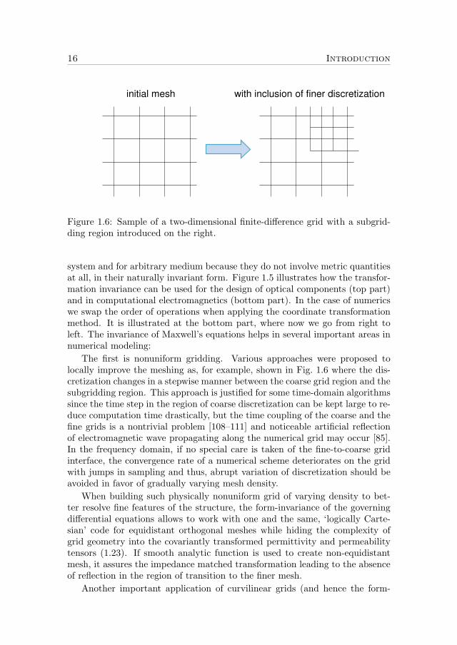
Figure 1.6: Sample of a two-dimensional finite-difference grid with a subgrid-ding region introduced on the right.
system and for arbitrary medium because they do not involve metric quantitiesat all, in their naturally invariant form. Figure 1.5 illustrates how the transfor-mation invariance can be used for the design of optical components (top part)and in computational electromagnetics (bottom part). In the case of numericswe swap the order of operations when applying the coordinate transformationmethod. It is illustrated at the bottom part, where now we go from right toleft. The invariance of Maxwell’s equations helps in several important areas innumerical modeling:
The first is nonuniform gridding. Various approaches were proposed tolocally improve the meshing as, for example, shown in Fig. 1.6 where the dis-cretization changes in a stepwise manner between the coarse grid region and thesubgridding region. This approach is justified for some time-domain algorithmssince the time step in the region of coarse discretization can be kept large to re-duce computation time drastically, but the time coupling of the coarse and thefine grids is a nontrivial problem [108–111] and noticeable artificial reflectionof electromagnetic wave propagating along the numerical grid may occur [85].In the frequency domain, if no special care is taken of the fine-to-coarse gridinterface, the convergence rate of a numerical scheme deteriorates on the gridwith jumps in sampling and thus, abrupt variation of discretization should beavoided in favor of gradually varying mesh density.
When building such physically nonuniform grid of varying density to bet-ter resolve fine features of the structure, the form-invariance of the governingdifferential equations allows to work with one and the same, ‘logically Carte-sian’ code for equidistant orthogonal meshes while hiding the complexity ofgrid geometry into the covariantly transformed permittivity and permeabilitytensors (1.23). If smooth analytic function is used to create non-equidistantmesh, it assures the impedance matched transformation leading to the absenceof reflection in the region of transition to the finer mesh.
Another important application of curvilinear grids (and hence the form-
1.3 Electromagnetics from computational perspective 17
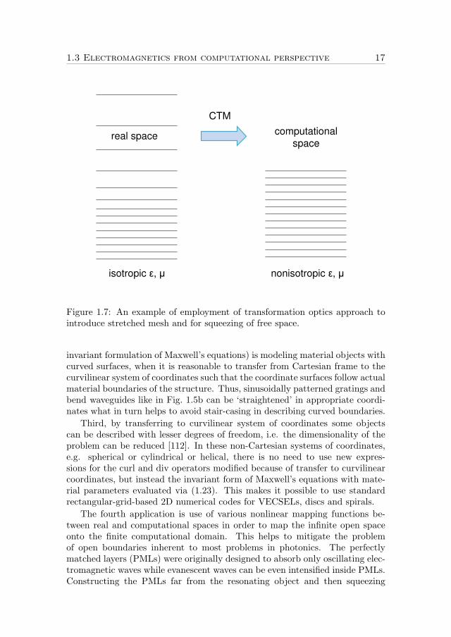
Figure 1.7: An example of employment of transformation optics approach tointroduce stretched mesh and for squeezing of free space.
invariant formulation of Maxwell’s equations) is modeling material objects withcurved surfaces, when it is reasonable to transfer from Cartesian frame to thecurvilinear system of coordinates such that the coordinate surfaces follow actualmaterial boundaries of the structure. Thus, sinusoidally patterned gratings andbend waveguides like in Fig. 1.5b can be ‘straightened’ in appropriate coordi-nates what in turn helps to avoid stair-casing in describing curved boundaries.
Third, by transferring to curvilinear system of coordinates some objectscan be described with lesser degrees of freedom, i.e. the dimensionality of theproblem can be reduced [112]. In these non-Cartesian systems of coordinates,e.g. spherical or cylindrical or helical, there is no need to use new expres-sions for the curl and div operators modified because of transfer to curvilinearcoordinates, but instead the invariant form of Maxwell’s equations with mate-rial parameters evaluated via (1.23). This makes it possible to use standardrectangular-grid-based 2D numerical codes for VECSELs, discs and spirals.
The fourth application is use of various nonlinear mapping functions be-tween real and computational spaces in order to map the infinite open spaceonto the finite computational domain. This helps to mitigate the problemof open boundaries inherent to most problems in photonics. The perfectlymatched layers (PMLs) were originally designed to absorb only oscillating elec-tromagnetic waves while evanescent waves can be even intensified inside PMLs.Constructing the PMLs far from the resonating object and then squeezing

18 Introduction
the PML-to-resonator distance [113] prevents perturbing the solution by theevanescent field tails originating from hot spots in nanostructured objects, forexample, near sharp metal edges.
Thus we see that computational methods can benefit a lot from using the in-variance of Maxwell’s equations, and below in this thesis we use this invariancefor free-space squeezing and nonuniform mesh construction.
1.4 The aim and outline of this thesis
The importance of efficient simulation tools for the design of nanophotonic de-vices is reflected by the rapid growth of the market of commercial software prod-ucts for photonics in the last decade; moreover, widespread became the prac-tice of using commercial black-box software for photonics simulations publishedeven in the most highly ranked journals like Nature. Extensive benchmarks forboth commercial and in-house developed software for numerical photonics andplasmonics are being published [115–117]; interestingly, the finite-differencefrequency-domain (FDFD) method is not even listed in such benchmark com-
Figure 1.8: Table highlighting the performance of time- and frequency-domainmethods in different problems in nanophotonics, from [114].

1.4 The aim and outline of this thesis 19
parisons.In this thesis we simulate fairly complicated photonic and plasmonic struc-
tures for which we find the FDFD method the best choice. In particular, weconsider the eigenmodes in PhC membrane based and nanobeam resonators,and light propagation through subwavelength metallic gratings whose periodto slit width ratio reaches 104 and more. From Fig. 1.8 with a table comparingthe time- versus frequency-domain methods published in a recent review [114]it is clear that such structures are advantageous to be simulated in the fre-quency domain. The structured FDFD method is chosen as the simplest and,potentially, most efficient one.
Maxwell’s equations in their discretized form can be viewed not as someapproximated version of continuous formulation but as a self-consistent andrigorous way to describe optics in condensed matter. Indeed, Maxwell’s equa-tions written for small volume (termed computational cell in the context of thefinite-difference modeling) can be interpreted as the integral equations [118];moreover, the placement of components on the staggered Yee grid correspondsto the geometric nature of oscillating electromagnetic waves. Thus the mainorigin of numerical errors in direct methods lies not in the discretization of thestructure but rather in other approximations such as the substitution of openspace with the PMLs and treatment of object boundaries with staircasing ordielectric index averaging approximations.
After sketching the FDTD formulation and its use in finding the eigenfre-quency and Q-factor of a photonic-crystal membrane resonator in Chapter 2,we formulate the FDFD method in its two versions, one for the eigenmodeanalysis and another one for monochromatic wave propagation modeling, inChapter 3. Two examples of application of the FDFD method to the eigen-mode analysis in photonic-crystal resonators follow in Chapter 4: a photonic-crystal membrane based cavity and an elongated nanobeam PhC cavity. Thenin Chapter 5 the coupling of two and more cavities is analyzed; and in Chapter 6the FDFD method is applied to modeling light propagation and enhancementin extremely-sub-wavelength metal gratings in a broad frequency range.
As regards numerical aspects of modeling, our emphasis is on the choice ofreasonable computational domain size and buffer layer width, use of squeezetransform layers in combination with PMLs to mimic infinite open space, andconstruction of grids of varying density to better resolve small features in thenanostructured materials. These issues, especially the construction (and place-ment) of absorbing boundaries, are not yet completely settled in the electro-magnetic modeling community, which is indicated, for example, by the absenceof the option to use absorbing boundaries in the eigenmode solver modulesof such popular commercial software products as CST Microwave Studio orComsol Multiphysics.


Chapter 2
Finite-differencetime-domain method forresonators
Possessing all-embracing universality, time-domain analysis has firmly enteredcomputational electromagnetics and rightfully holds the first place by quantityof diverse modeling tasks that they can solve. Commercialized finite-differencetime-domain (FDTD) and transient finite-element method are everyday toolsin hands of experimentalists demanding multiple routine calculations of deviceoperation under fabrication constraints and imperfections. So there is no sur-prise that before passing to the FDFD algorithm we start by getting acquaintedwith its time-domain counterpart — the FDTD method — that already becamea standard tool in nanophotonics.
One of the main advantages of transient algorithms is the possibility tosimulate large structures (Fig. 1.8). Moreover, parallelization of the FDTDsimulations has already become a well-established procedure for modeling ofgigantic numerical problems. As for frequency-domain methods, parallelizationis also possible here, however, it is not that well established and thus simulationof large models is not a strong point here. As another essential advantage wecan mention obtaining a spectral response from the structure in the whole rangeof frequencies during a single run with excitation by a broadband pulse.
In addition, the FDTD algorithm has many extensions starting from in-clusion of nonlinearity and to modeling coupled Maxwell-Bloch equations. Todescribe an ensemble of active quantum dots or nonlinear medium in nanos-tructured environment an additional polarization term for the active material isusually included into the FDTD-discretized Maxwell-Ampere equation to takeinto account multiple reemission and reabsorption of light by quantum dotsor nonlinear enhancement. Practically, similar polarization term is introducedalso to describe metal dispersion in time-domain approaches.

22 Finite-difference time-domain method for resonators
x
y
z
Ez
Ex
EyHy
Hx
Hz
i j k - cell
PMC
PMC
PMC
PEC
(a) (b)
Figure 2.1: (a) Unit Yee cell with spatial positions of electric and magnetic fieldcomponents. (b) Location of the perfect electric or magnetic conductor walls(PEC and PMC, respectlively) at the outer boundaries of the computationaldomain.
2.1 Formulation of the FDTD method
2.1.1 Spatial discretization
The FDTD algorithm is based on discretization of Maxwell’s curl equationsin real space and tracing of the source field distribution in time [119]. Wediscretize the object according to the Yee mesh [120], Fig. 2.1a, and constructthree different permittivity and three permeability arrays for each field com-ponent as their meshes are shifted spatially. Then we introduce six arrays forelectromagnetic field components and use the initial values in these arrays andsome given source field distribution (in space and time) to calculate the fieldevolution as governed by Maxwell’s equations.
The source-free Maxwell’s equations can be written as
∇f ×E = −µ∂tH, ∇f · µH = 0 (2.1a)
∇b ×H = ϵ ∂tE, ∇b · ϵE = 0 (2.1b)
where subscripts f and b near the operators are introduced to point out theirdifferent action on a staggered Yee mesh [120], Fig.2.1a, which can be illustratedfor differential of some vector component A along the x-direction:
∆fA = A(x+∆x)−A(x) (2.2a)
∆bA = A(x)−A(x−∆x) (2.2b)
The subscript f means that the curl and div operators are constructed on thebasis of the forward finite difference scheme, the subscript b implies usage of

2.1 Formulation of the FDTD method 23
the backward finite differences. Each of forward or backward differences 2.2by themselves imply first-order accurate scheme if their result is assigned toone of the side points. However, on the staggered Yee mesh these differentials∆f,bA are used to define dual-mesh field components positioned in the points inbetween the given mesh nodes. Thus in fact our scheme is a central-differencescheme giving second-order convergence.
Let’s define now the differential operators if our vector fields are representedby three-dimensional arrays on Yee mesh. For example, 3D forward F...n... andbackward B...n... derivatives acting along nth direction (corresponding to x, yor z axis) with a step ∆hn on some field component A:
(FnA)...in... =1
∆hn(A...in+1... −A...in...) (2.3a)
(BnA)...in... =1
∆hn(A...in... −A...in−1...) (2.3b)
This operators are analogous to the MatLab based function diff. With thisdefinition of difference matrices we can easily obtain the boundary conditionon the borders of the computational domain as depicted in Fig. 2.1b.
As on staggered Yee grid the divergence equations in Eq. (2.1) are automat-ically fulfilled [119] we are now interested only in constructing of curl operatorswith use of already defined differential operators. For example, (∇f ×E)x com-ponent can be written as FyEz−FzEy what proportional to the time derivativeof magnetic field Hx.
2.1.2 Time stepping
Having defined space derivatives we can pass to writing update equations forfield evolution in time (described by the superscript j):
Ej+1x = Ej
x +∆t
ϵ(ByH
jz −BzH
jy) (2.4a)
Ej+1y = Ej
y +∆t
ϵ(BzH
jx −BxH
jz ) (2.4b)
Ej+1z = Ej
z +∆t
ϵ(BxH
jy −ByH
jx) (2.4c)
Hj+1x = Hj
x − ∆t
µ(FyE
j+1z − FzE
j+1y ) (2.4d)
Hj+1y = Hj
y − ∆t
µ(FzE
j+1x − FxE
j+1z ) (2.4e)
Hj+1z = Hj
z − ∆t
µ(FxE
j+1y − FyE
j+1x ) (2.4f)
If a source is defined at some place in the computational domain, prop-agation of light from this source in time and space can be obtained startingfrom Eq. (2.4a–c) by inserting some initial values of fields corresponding to this

24 Finite-difference time-domain method for resonators
source. Then electric field at the next time step might be evaluated straight-forwardly and if inserted to Eq. (2.4d–f) magnetic field components in thenext time step can also be found. This time staggered calculation of electricand magnetic field components is often called leapfrogging. Proceeding thetime cycle gives evolution of fields in time and space which was searched for.It could be shown that the necessary condition for the stability of the time-stepping algorithm is the Courant criterium relating the Yee cell size and thetime step [119]:
∆t <1
c√1/∆x2 + 1/∆y2 + 1/∆z2
(2.5)
2.2 Q-factor evaluation with the FDTD method
2.2.1 Excitation of single resonance in the time domain
To find all the modes for the given cavity when no preliminary informationabout resonance frequencies exists, a broad-band excitation pulse is launchedin the system. In the case of multiple resonance excitation we see characteristicmodulation of the electromagnetic field with time caused by superposition ofthe modes oscillation. For a 2D holey PhC slab with the cavity formed byomitting one hole (Fig. 2.2a) the evolution of the electric field is shown inFig. 2.2b. The shape of field envelope is evidently due to superposition ofseveral resonances giving the characteristic beating.
In Fig. 2.3 two fast Fourier transforms (FFT) are compared: the one in-cluding excitation pulse, the other one made from the field decay after turningoff the source. From the first spectrum we are not able to predict the numberof resonances and their wavelengths, while from Fig. 2.3b we can define two
1000 2000 3000 4000 5000 6000time steps
-1000
-500
0
500
1000
Hx1
(a) (b)
Figure 2.2: (a) One-missing-hole 2D-PhC microcavity. Dipole source polarizedin perpendicular z direction is in the middle, two detectors shown as arrows.Lattice constant a = 254nm, air holes radius r = 0.3a, n = 3.6. Square griddiscretization is 10 nm. (b) Field evolution in the case of broad-band excitationrecorded on the right vertical detector in Fig. 2.2a.

2.2 Q-factor evaluation with the FDTD method 25
1 1.2 1.4 1.6 1.8 2
0
2000
4000
6000
8000
10000
l, mm
Hx
1.1 1.2 1.3 1.4 1.5 1.6 1.7
l, mm
0
2000
4000
6000
8000
10000
Hx
(a) (b)
(c)
Figure 2.3: (a) Wavelength dependence of the field on two detectors, when FFTwas made for the whole time (excitation + decay). (b) Wavelength dependenceof the field on two detectors, when FFT was made only for field decay (afterturning off the source). (c) Snapshot of Ez (left) andHx (right) field componentin a one-missing-hole membrane from Fig. 2.2a.
resonance wavelengths corresponding to two cavity modes. If excitation pulseis included into FFT then normalization of obtained cavity spectrum to FFTof the source should be made to extract the Q-factor and resonance wavelengthof the mode correctly.
The duration, polarization and position of the source can play an importantrole in the excitation of a single resonance. To excite only one mode at λ =1.28µm, we need to tune the source bandwidth so narrow as to do not overlapwith the second resonance at λ = 1.5µm. With use of modulation theorem [121]we can approximately estimate the position of resonances if excitation signalis modulated. In Fig. 2.3c the distribution of the fields was detected at asome moment in time after turning off the source. Besides appropriate choiceof excitation pulse, much care should be taken to assure the computationaldomain is large enough. Our simulations of low-Q photonic crystal membranecavities (Q around 100–200) using the FDTD-based Crystal Wave solver [85]gave stable results when the air cladding above the resonator was of about onewavelength wide.
The capabilities of the FDTD method to calculate high Q-factors are re-flected in its wide usage for designing photonic crystal based cavities [53–56,122, 123]. In these works featuring resonators with the highest reported Q-

26 Finite-difference time-domain method for resonators
factors, the Q extraction methods are based on the simplest approaches: thelorentzian fit after the FFT, tracing of electromagnetic field components ringdown, sometimes together with direct definition of Q through Eq. 1.6. Know-ing the resonance frequency ω0, the Q-factor can be defined with just oneelectromagnetic field oscillation period being traced. However, this ultra-fastprocedure is usually accompanied by other methods of extraction which re-quire vigourous postprocessing additionally to long execution time [56,124,125].Thus in a proposed huge variety of cavity designs based on structural modifica-tions in photonic crystals many alternative state-of-the art methods to calculateQ [55, 126, 126–129] are left unexploited at all. The possible reason for thatis a lack of comparison of different extraction methods with almost no cross-references between articles developing alternative techniques what complicatesthe choice of most suitable approach for the user.
2.2.2 Sphere benchmark: field components or energy den-sity?
In spherical coordinates, it is possible to investigate free oscillations of theelectromagnetic field in the sphere analytically. The quality factor is extractedfrom the imaginary part of resonance frequency. It depends on the dimension-less parameter ω0a/c (see §9.22 in [130]), where ω0 is the angular resonancefrequency, a the radius of the sphere and c the vacuum speed of light. Considerthe dipole mode TE101 for the sphere of refractive index nsphere = 6 embeddedin air. Its analytical Q-factor is Q = 43.17 at ω0a/c = 0.512 [131]. The reso-nant wavelength for the radius a = 0.16 µm is λ = 1.963 µm; it is used as a
(a) (b)
Figure 2.4: (a) Positions of a current source (close to the center) and detectors(d1–d5) in the nanosphere of radius a = 0.16µm and refractive index n = 6 inair. Dimensions of the computational domain are (0.8µm)3, the grid resolutionis 5 nm, PMLs width is 8 grid points. (b) Snapshot of electric field in thedielectric nanosphere after turning off the source.

2.2 Q-factor evaluation with the FDTD method 27
2 3 4 5 6 7
x 104
−1
−0.8
−0.6
−0.4
−0.2
0
0.2
0.4
0.6
0.8
1
time step
Ex field decay from d1envelope formed by maxima pointsenvelope formed by minima points
(a)
0 5000 10000 15000 200000
0.05
0.1
0.15
0.2
0.25
time step
oscillating energy density from d1maxima pointsminima pointsperiod−averaged energy density
Q = 43.19
(b)
Figure 2.5: Analysis of field evolution in the case of the dipole mode excitationin the sphere from Fig. 2.4a. (a) Evolution of the Ex field component withpositive and negative envelopes. (b) Oscillating and period-averaged energydensities.

28 Finite-difference time-domain method for resonators
central wavelength of a narrow-band signal to excite the sphere. The source ispositioned in close proximity to the center of the sphere and five point detec-tors are located at different points inside and outside the sphere as shown inFig. 2.4a. We made the FDTD calculations with use of the commercial packageCrystal Wave [85]. By plotting the Ex-field distribution (Fig. 2.4b we see thatit is indeed a dipole mode.
According to Eq. (1.1) the Q-factor of a mode characterizes the cavity whenthere is no any influence from a source. Therefore, excitation pulses of finiteduration are used. The field decay is analyzed to findQ and ω0 after the pulse isswitched off [132]. Q and ω0 are obtained from the evolution of electromagneticfield components: a lorentzian fit to the squared absolute value of the Fouriertransformation A(ω) = FT [A(t)], and an exponential fit to the envelope of A(t)formed by the minima or maxima points of an oscillating electromagnetic field,
1 2 3 4 50
1
2
3Ex
Q e
r, %
1 2 3 4 50
10
20Hx
Q e
r, %
Q e
r, %
1 2 3 4 50
50
Ey
Q e
r, %
1 2 3 4 50123
Hy
1 2 3 4 50
1020
Ez
Q e
r, %
1 2 3 4 50
0.5
1Hz
Q e
r, %
1 2 3 4 50
0.5
1
λ er
, %
Detectors
All field components
1 2 3 4 50
0.5
1
Q e
r, %
Detectors
UP19 %
54 % 56 %
Figure 2.6: Top six graphs for each of the electromagnetic field componentsillustrate a Q-factor error given by the three methods: black bars– the expo-nential fit to the envelope of the field formed by maxima points in the timedomain, grey–the same but with the minima points, white–the lorentzian fit inthe frequency domain. Bottom left: wavelength error from the lorentzian fit inthe frequency domain to all six field components. Bottom right: Q-factor errorfrom the exponential fit to the period-averaged energy density U and Poyntingvector P . Numbers on horizontal axis in all figures correspond to five differentdetectors.

2.3 Transfer to the frequency domain: motivation 29
Fig. 2.5a. Here A(t) designates any of the field components, which in the FDTDcalculations are normally kept as real values. The oscillating energy densityw evaluated directly through computed field components is a time-oscillatingfunction. In order to get an exponential decay and to define the Q-factor it isperiod-averaged as shown in Fig. 2.5b.
Comparing time periods of signals straightforwardly from Fig. 2.5a andFig. 2.5b, we can find that evolution of energy density is described by theFDTD algorithm with better maintenance of periodicity (counted directly intime steps) than for a single electromagnetic component: if for energy densityinaccuracy in period comprises no more than one time step, for some fieldcomponents it might reach several time steps. Thus energy density calculationbalance simulation errors given by all field components in such a natural waythat they are reduced compared to a simple averaging procedure.
The diagram in Fig. 2.6 shows relative Q-factor and resonance wavelengtherrors given by different methods. While fitting in the time domain as shownin Fig. 2.5, the angular frequency ω0 was taken equal to its analytical value,so no additional error is introduced by inaccuracy in ω0. Nevertheless, singleelectric or magnetic field components give unstable Q-factor with unexpectedlyhigh relative errors in some cases, while the energy density fitting has an errorbelow 0.8%. So we conclude that the most accurate and robust way to definequality factor is via the exponential fit to the time-averaged energy density.In this case there is no need to collect information through the whole domainand it is enough to use only one point detector, placed arbitrarily inside oroutside the sphere. In the case of multiple resonances, the period-averagedenergy density will not be a single-exponential function anymore and we areforced to return to the analysis of single field components. This should be donewith care; averaging of calculated results for Q-factor over the whole domainand for all field components is recommended.
2.3 Transfer to the frequency domain: motiva-tion
Among numerical tools to determine cavity mode characteristics, one of themost widely used is the finite-difference time-domain (FDTD) method. Inthis chapter we compared the most robust extraction methods for analyticalexample of a sphere. It was shown that the obtained Q-factor values differsignificantly from one extraction method to another and the electromagneticfield component being analyzed. The reliability of the single field componentextraction method is put under doubt, and energy density analysis is foundto be clearly advantageous. Yet many extraction methods rely on the analysisof single field components and some authors report severe problems with theFDTD technique for finding resonances with Q higher than 103 [133]. Goinga bit ahead in Table 2.1 we list FDTD computational domain and cycle pa-rameters together with some extraction methods, and compare them with the

30 Finite-difference time-domain method for resonators
Time domain Frequency domain
Post-processing ring-down of fields;Harminv; Lorentzianfit; energy loss percycle; Pade approx-imation; Prony’salgorithm; pencil-of-function method
not needed
Adjacent eigenmodes mixed naturally separatedAir buffer layers thick moderateMemory usage moderate highTypical run time day hour
Table 2.1: Table comparing extraction methods, computational and user ef-forts for defining resonator characteristics with the time- and frequency-domainfinite-difference algorithms.
features of the frequency-domain simulation tools. We see strong motivation todevelop the frequency-domain counterparts of FDTD approaches what is donein the next chapters of the thesis. For the user of the numerical method a greatadvantage of the frequency domain technique over the time domain analoguesis elimination of postprocessing steps in some tasks, e.g., no need to go throughthe analysis of time-domain signals to extract the Q-factor of a cavity mode,besides in many tasks the run time is greatly reduced as well. And if we areinterested in field distribution in the structure illuminated by the plane wave ofcertain frequency, frequency-domain method is also the tool of natural choice.
Chapter 3
Finite-differencefrequency-domain method
As an alternative to the time-domain modeling, we employ the 3D finite-difference frequency-domain (FDFD) method with the perfectly matched lay-ers (PMLs) and free space squeezing. The algorithm can be formulated withease for solution of a multitude of problems, for example, those involving ar-bitrarily dispersive materials and periodic media or modeling transmitted andreflected electromagnetic fields in the presence of monochromatic light sources.The quality factor and resonance frequency in the frequency domain appearstraightforwardly, require no post-processing and do not depend on a choice ofa specific fitting procedure. A typical FDFD run takes minutes while an FDTDsimulation runs up to several hours for a comparable system and hardware.The FDFD technique applied to a particular system manipulates entire arraysrepresenting electromagnetic field components and material permittivity andpermeability on a structured grid, thus it is not so cumbersome and dependenton the mesh generation subroutines as the finite-element method [134].
From the early 1980’s, three-dimensional finite-difference and finite-integraltechniques in the frequency domain were applied to modeling of closed cavitiesand metal structures [135–140]. Today 3D frequency-domain method is usedwidely in microwave cavity analysis [114, 141, 142] and, to a lesser extent, inphotonic bandgap computations where Bloch-periodic boundary eigenproblemis solved [143, 144]. Analysis of open photonic resonators with the 3D FDFDmethod was problematic, in contrast to photonic band calculations, for twomain reasons: first, much larger, i.e., multiple-lattice-constant pieces of PhCmatrices must be considered; second, nontrivial absorbing boundaries like theperfectly matched layers placed at sufficient distance from the modeled res-onator are to be used instead of simple Bloch-periodic walls. These issues arespecifically addressed when formulating and using the FDFD method in thecurrent and subsequent chapters.

32 Finite-difference frequency-domain method
3.1 Two variations
3.1.1 Monochromatic wave transmission analysis
Maxwell’s curl equations (1.20a) for the fields E, H can be written in thefrequency domain, after substituting ∂t = −iω, as
∇×E = iωµH, (3.1a)
∇×H = −iωϵE+ J, (3.1b)
where J is the amplitude of electric current playing the role of a source forharmonic (monohromatic) light of frequency ω. These equations can be viewedas a linear system which, at a given excitation J and frequency parameter ω,can be solved to obtain the ‘joint’ vector (E,H)T :[
∇× −iωµiωϵ ∇×
] [EH
]=
[0J
]. (3.2)
Yet it would be better to reduce this system by combining the two equationsfrom (3.1a) to arrive at(
µ−1∇× ϵ−1∇×−ω2I)H = S. (3.3)
with the source term S = µ−1∇×ϵ−1J on the right hand side. To excite a planewave, we can specify the amplitude of excitation current J along some plane inthe computational domain, with Bloch-periodic boundaries in the directions ofthat plane.
For better numerical performance of some linear algebra algorithms it wouldbe advantageous to have the system matrix symmetrized; this can be actuallydone easily by scaling the coordinates so that H =
õH, S =
√µS, and(√
µ−1 ∇× ϵ−1∇×√µ−1 − ω2I
)H = S. (3.4)
To solve (3.4) directly, one can factorize the equation matrix
M =√µ−1 ∇× ϵ−1∇×
√µ−1 − ω2I. (3.5)
After (3.4) being solved for the normalized magnetic field H, one can easilyrestore all the electromagnetic fields and other quantities, for example, thePoynting vector in order to calculate reflection and transmission energy coeffi-cients.
3.1.2 Eigenmode analysis
Omitting the current source term in Maxwell’s curl equations (3.1a) we have
∇×E = iωµH (3.6a)
∇×H = −iωϵE. (3.6b)

3.1 Two variations 33
Again, already at this stage this Maxwell’s system can be seen as an eigenprob-lem in ω and the ‘joint’ field (E,H)T :[
0 1−iϵ∇×
1iµ∇× 0
] [EH
]= ω
[EH
]. (3.7)
This is not a good setting for further numerical solving however, because al-though the eigenmatrix in (3.7) is certainly very sparse, its dimensionality canbe halved by combining (3.6a) and (3.6b) into the system of second-order dif-ferential equations, for example
µ−1∇× ϵ−1∇×H = ω2H. (3.8)
This can be further symmetrized upon the substitution H ≡ √µH:√
µ−1 ∇× ϵ−1∇×√µ−1 H = ω2H. (3.9)
Although the eigenmatrix in (3.9) differs from M (3.5), if we resort to theshift-and-invert method to solve the eigenproblem (3.9) iteratively for only afew frequencies around some target frequency ωtgt then we need, again, therecipe to calculate M\H repeatedly during the iteration process. The waywhich is robust and fast (but memory consuming) is to factorize M = LU —that is, to do exactly the same step which we can employ for solving (3.4) inthe monochromatic wave propagation modeling.
Due to the presence of the PMLs the eigenmatrix Θ =√
µ−1 ∇× ϵ−1∇×√µ−1 in (3.9) is complex nonhermitian even if the constitutive materials are
non-absorptive. Such nonhermitian problem leads to complex eigenfrequenciesω = ω′ + iω′′ with their real parts giving the resonance frequencies and theimaginary parts directly connected to the Q-factors:
ω0 = ω′, Q =ω′
2ω′′ . (3.10)
For a sufficiently good resonator we always have ω′ ≫ ω′′, so that in numericalmodeling, comparable absolute errors in ω′ and ω′′, δω′ ≈ δω′′, lead to muchhigher relative errors in the Q-factor values: δω′/ω′ ≪ δω′′/ω′′. This is exactlywhat we will see in the numeric examples below. Furthermore, the Q-factoris more sensitive to the PML parameters (their placement, absorption profile,etc.) as it arises entirely due to the introduction of artificial imaginary partsin ϵ and µ within the PMLs, while for the eigenwavelength the PMLs can beseen as just a perturbation.
Additional complication arises through the frequency dependence of mate-rial tensors ϵ and/or µ and hence the eigenmatrix Θ. When resonator containsmetal components or any other materials whose dispersion should accuratelybe taken into account, one can start with some guess ω0 for the eigenfrequencyand attempt repetitive solving of the linearized eigenproblem with Θ = Θ(ω0)

34 Finite-difference frequency-domain method
for the eigenfrequency ω1, then with Θ = Θ(ω1) for ω2 etc., until a convergencecriterion |ωi − ωi−1| < ∆ω is met. But, unlike material dispersion, the PMLdispersion is a mathematical artifact inessential to the user of a numerical tooland, due to certain robustness of PML performance with respect to the val-ues of PML conductivity, the PML dispersion can be ignored in the frequencydomain by putting Θ = Θ(ω0) in the eigenproblem. If this ω0 used to definethe PML maximum conductivity is not too far from the exact eigenfrequency,one can expect that an error introduced by non-optimal PML conductivity isnegligible.
3.2 Discretization matters
3.2.1 Discretization of computational domain interior
In the discretized form Eq. (3.9) reads
ω2
Hx
Hy
Hz
=√
µ−1
0 −Fz Fy
Fz 0 −Fx
−Fy Fx 0
ϵ−1
×
0 −Bz By
Bz 0 −Bx
−By Bx 0
√µ−1
Hx
Hy
Hz
(3.11)
where Hx,y,z are column-vectors of length ntot each, ntot = nxnynz is thetotal number of grid nodes in the domain. It is assumed that µ is representedby a diagonal matrix (which is not always true for ϵ upon its polarization-sensitive averaging at material boundaries, see Ref. [145]) so that µ−1 canbe split in its square roots trivially in order to get symmetrized eigenmatrixΘ =
√µ−1 ∇× ϵ−1∇×
√µ−1. We define 1D forward difference matrix fnx of
size nx × nx acting along x on the electric field component normal to x, forexample Ey:
fnx
E1
y...
Enx−1y
Enxy
=1
∆x
−1 1
. . .. . .
−1 1−1
E1y...
Enx−1y
Enxy
(3.12)
with ∆x being the grid step (which is constant in computational space but mayvary in physical coordinates). The matrices Fx,y,z of the size ntot × ntot are:
Fx = Inz ⊗ Iny ⊗ fnx ,
Fy = Inz ⊗ fny ⊗ Inx ,
Fz = fnz ⊗ Iny ⊗ Inx ,
(3.13)

3.2 Discretization matters 35
where Inj is the unit diagonal matrix of the size nj × nj , ⊗ is the Kroneckerproduct. Backward-difference matrices Bx,y,z are equal to the negative Fx,y,z
transposed. Thus, the final size of the eigenvalue matrix Θ is 3ntot×3ntot. Thecombination of forward and backward differentials acting on the Yee-staggeredelectric and magnetic fields allows second-order-accurate discretization of (3.9),at least locally. Numerical accuracy of the FDFD solution for various Cartesiandiscretization meshes was analyzed by Smith [146,147]; in particular, differentoffsets in location of field components within the primary cell were discussedwith conclusion that the most accurate is the classical Yee staggering [120]. Be-sides, Smith showed that the deviation of numerically determined wavenumbersfrom analytic ones is small only far below the Nuiquist wavenumbers. That is,the roughest sampling should be at least λ/10 to get reliable simulation results.
The chosen arrangement of electric and magnetic field components assumesplacing of the perfect magnetic conductor (PMC) boundary at the beginningand the perfect electric conductor (PEC) boundary at the end of each of thedomain extensions, as shown in Fig. 3.1. This is very convenient in modelingopen symmetric systems: by centering such system in an appropriate corner ofcomputational domain, we cut the system by a combination of the PMC andPEC planes according to the expected mode symmetry while covering three
x
dx
dx/2
dy/2dy
EE
x
z
,
}=0HH
x
z
,}=0
H H }=0y z,
E E }=0y z,
y
Ey
Ey
Ey
Ey Ey
EyEy
Ey
Ey
EyEy Ey Ey
Ey
Ey
EyEyEyEyEy
Ex
Ez
Hy
Hx
Hz
Figure 3.1: xy-cut of the Yee mesh with locations of the Ey nodes shownrelative to the computational domain boundaries (depicted with bold blacklines). The meshes for other components are obtained through linear shifts byhalf cell steps along the different coordinate axes.

36 Finite-difference frequency-domain method
remaining domain walls with absorbing boundary layers.Figure 3.1 is a guide for understanding how the field component grids are
located inside the computational domain with respect to each other and thedomain boundaries. We see that the gray frame representing the startingand ending planes of the nonzero Ey components grid has dimensions thatdo not coincide with the real domain size but are smaller. Shifts of this grayframe with Ey pixels by half or whole grid step size along different axes givemeshes for all other field components with the same total number of nodes inthe result. Note that Maxwell’s equations are local, i.e. they connect onlythe neighboring electric and magnetic field components; hence to reduce thebandwidth of the eigenmatrix it can be defined such that the field compo-nents are arranged as [Ex111 , Ey111 , Ez111 , Ex211 , Ey211 , Ez211 , . . . ]
T instead of[Ex111 , Ex211 , . . . , Ey111Ey211 , . . . , Ez111 , Ez211 , . . . ]
T . The former case leads to asignificant decrease of the matrix bandwidth and, hence, to much lesser memoryrequirements when performing LU factorization.
In Appendix B we compare the FDFD and FEM efficiencies for solutionof Helmholtz equation for rectangular 2D PEC cavity. The sampling and sizeof the cavity were kept the same for both methods. In general, the FDFDtechnique has performance comparable with the FEM method what makesmuch simpler FDFD structured formulation perspective. Of course, this is justan initial estimation and detailed comparison is needed for more complicatedgeometries and boundary settings.
Non-equidistant mesh
Non-equidistant grid can be introduced if transformation function f(xcomp)from computational xcomp to physical xphys coordinates is known:
xphys = f(xcomp) (3.14)
Discretization of the domain is first done in computational coordinates toobtain strictly equidistant mesh and then physical mesh nodes are calculated.Physical mesh is defined in any orthogonal system of coordinates, i.e. carte-sian, spherical, cylindrical, etc. An example of algorithm to incorporate non-equidistant physical grid within the logically cartesian code may look like:
1. Find domain size in computational coordinates, xendcomp, by solving Eq. 3.14
for xcomp: xendcomp = f−1(xend
phys)
2. Discretize the domain in computational coordinates with equidistant gridand find the corresponding physical mesh node coordinates through Eq. 3.14
3. In physical non-equidistant orthogonal coordinates do the permittivityaveraging at material boundaries
4. Using the jacobian [J ] =∂xcomp
∂xphys= 1
f ′(xcomp)and Eq. 1.23 (with substitu-
tion x′ → xcomp, x → xphys) compute ϵcomp and µcomp

3.2 Discretization matters 37
103
104
105
10−2
10−1
100
101
102
103
104
Total number of nodes n
Exe
cutio
n tim
e, s
ec
ε and µ generatedeigenmatrix assembledeigenprblem solved
Figure 3.2: Execution time of three major FDFD algorithm blocks: (i) genera-tion of ϵ and µ arrays representing material distribution within the domain and,if necessary, PMLs and STLs; (ii) assembling sparse eigenmatrix to be solved;(iii) solving the eigenmatrix with Matlab’s eigs function. Simulations were per-formed on a 16 Gb station for the dipole mode in the spherical resonator fromSection 2.2.2.
5. After the FDFD run, physical field components Fphys are found as Fphys =[J ]Fcomp
Notice that f(xcomp) is usually a nonlinear function and deriving explicitanalytic expression for the inverse, f−1(xphys) = xcomp, is often impossible.Thus in the first stage listed above, to find xphys from the given xcomp, tran-scendental Eq. 3.14 is typically solved. This might be computationally and timedemanding and it is preferable to do it only for a few nodes, not the whole mesh.This is also the reason why we start by specifying analytic form of f(xcomp)but not f−1(xphys) because in the latter case transcendental equation shouldbe solved for all mesh nodes to calculate physical coordinates.
Time consumption
Time consumption given by discretization and simulation of a square domain ona 16Gb machine is shown in Fig. 3.2 on the example of the dipole mode in thespherical resonator (exact parameters can be found in Section 2.2.2). Generat-ing permittivity and permeability arrays and construction of a total eigenvaluematrix normally takes seconds or minutes at most. The eigenmatrix assem-bly time is linear with ntot = nxnynz while the ϵ array generation time scales
in 3D as linear measure squared, n2/3tot , because its major overhead is treating

38 Finite-difference frequency-domain method
grid cells crossed by material boundaries. We pass the assembled eigenmatrixto the Matlab function eigs which provides an interface to the Fortran-basedARPACK [148] library for solving sparse eigenvalue problems iteratively; how-ever, we use direct LU factorization at the shift-and-invert step. This is muchmore memory-consuming but also more reliable and universal than iterativealgebraic methods which require very careful and problem-dependent precon-ditioning. The solution time and the maximal resolution for the given memorylimit depend strongly on the structure of the eigenmatrix. Thus, elongatedcavities give eigenmatrices with much smaller bandwidth and hence essentiallylarger maximal total number of grid nodes ntot than structures requiring a cu-bic domain. Characteristic run time in 3D modeling is about an hour or two ifyou are close to the memory limit on a 16Gb machine.
3.2.2 Boundary conditions and domain reduction
Zero boundaries
The chosen arrangement of electric and magnetic field components assumesplacing of the perfect magnetic conductor (PMC) boundary at the beginningand the perfect electric conductor (PEC) boundary at the end of each of the do-main extensions, as shown in Fig. 3.1. Expressions for the elementary forwardand backward differentials:
f =1
∆h
−1 1
. . .
−1 1−1
, b =1
∆h
1−1 1
. . .
−1 1
(3.15)
show that we get zero values at the interfaces of the computational domainfor some field components. For example, the last row in the matrix fnx givesdifferential of the electric field at the end point proportional to 0−Enx
y implyingthe y-directed electric field component vanishes at the nx+1 point. Thus in allYee-mesh cells located at the nx +1 plane we have a perfect electric conductor(PEC) boundary with nullified tangential components Ey = 0, Ez = 0. If weare going to consider this PEC boundary as a plane of symmetry then at the x =nx+1 plane the tangential electric and normal magnetic components have zerovalues; all the rest normal electric and tangential magnetic components preservethe same values as at the x = nx plane, being symmetrically reflected at thePEC-boundary. For the virtual x = nx+2 plane we have negative reflection forall antisymmetric components, and positive reflection for the symmetric ones.
From Eqs. (3.12) we see that the forward curl operator ∇e acting on theelectric field leads to absence of its tangential components at the top borders ofthe domain, that is the upper and the most right planes in Fig. 2.1b, Fig. 3.1.Corresponding PEC boundary condition planes are shown schematically in thefigure. The curl operator ∇h acting on magnetic field is composed from back-ward differences matrices Vx,y,z. The latter nullify magnetic tangential compo-

3.2 Discretization matters 39
nents at the bottom plane interfaces passing through the origin of the domain,i.e. most left and bottom borders, see Fig. 2.1b and Fig. 3.1. The perfectmagnetic conductor (PMC) boundary conditions are also depicted there. Thisautomatical fulfilment of boundary conditions without additional changes ineigenmatrix is very convenient also for memory savings as we in general do nottake into account nodes lying at the edges of the domain.
The position of PEC and PMC planes are directly connected with our for-mulation of finite-differences matrices and it is important that numbering ofall arrays should start from the bottom left corner and finish in the top rightcorner. This rule should be followed while discretizing structure to get ϵ and µprofiles.
Domain reduction with PEC and PMC planes
P M C
P
M
C
x
y
P E C
P
E
C
P E C
P
E
C
P
M
C
P
M
C
P
E
C
P M C
P E C
P M C
Figure 3.3: Boundary conditions arising from reduction of the domain showedin xy-cut. Arrows in the corners indicate points to start indexing.
Most of the optical systems used as resonators have symmetrical form, there-fore it is computationally favorable to discretize not a whole domain but onlyits part thus increasing maximum possible resolution at least twice. The alter-nating boundary conditions surrounding the domain in Fig. 3.1 turn out to bevery convenient, when we want to exploit planes of symmetry. Indeed, we donot need to put any additional efforts to implement PEC or PMC conditionsin the code. Just by discretization different pieces of symmetric systems whilecovering remaining domain walls with absorbing boundary layers, we can con-sider optical structures with various number of mirror-symmetrical planes and

40 Finite-difference frequency-domain method
solve the eigenvalue problem for modes with diverse symmetries.
If an origin of coordinates coincides with the center of symmetry of a res-onator the easiest way to make domain reduction within the same code is toconsider only positive or negative half-axe for each coordinate thus allowingPEC or PMC planes to cut away unnecessary symmetric parts of the struc-ture. It is illustrated in Fig. 3.3 on the example of x− y plane passing throughthe center of computational domain. Thus, for objects with three perpendicu-lar planes of symmetry we specify only one of the eight coordinate octants tobe sampled and simulated.
Periodic boundaries
Treatment of structures with periodicity is one of the essential advantageous ofthe frequency domain technique. Bloch periodicity along some axis x: H(x +P ) = eikxPH(x), where kx is the wave vector, can be incorporated into 1Ddifferential by substituting zeros in Eq. 3.15:
f =1
∆h
−1 1
. . .
−1 1
eikP −1
, b =1
∆h
1 −e−ikP
−1 1. . .
−1 1
,
(3.16)Note, that for periodic boundaries discretization scheme in Fig. 3.1 is not suit-able. In particular, the boundaries of computational domain should coincidewith mesh nodes for one of the field components to enforce strictly periodicboundary conditions, i.e. half Yee cell offset is not required.
Open boundaries
Construction of efficient absorbing boundaries for modeling open photonic sys-tems is not a trivial task. Profound research was done on optimizing thePMLs — their thickness, conductivity profile, and frequency dispersion — forbetter absorption of oscillatory waves. In many real-life simulations however,one deals routinely with an admixture of evanescent field spreading from a pho-tonic structure; it is this evanescent field that prevents PMLs be constructedstarting immediately from the boundaries of the structure. This is bad newssince increased computation domain size amounts to increased computer mem-ory consumption, especially in 3D modeling. To squeeze the buffer physicalspace into the interval [a0, b] (where a0 is the most extended point of the mod-eled object and b the computational domain boundary) most efficiently, wecombine standard PMLs with free space mapping, so that the wavelength-dependent buffer “stretch function” in x (and similarly y and z) direction is
s(xcomp, λ) = ζ(xcomp)− iσmax(λ) η(xcomp). (3.17)

3.2 Discretization matters 41
0 0.2 0.4 0.6 0.8 10
1
2
3
4
5
xcomp
x phys
x/(1−x)2/π*tan(xπ/2)atanh(x)x
Figure 3.4: Examples of the mapping function xphys = xphys(xcomp) comparedto the identity line xphys = xcomp (plotted in bold).
Here ζ(xcomp) = ∂xcomp/∂xphys is the derivative of the chosen real spacesqueezing function; the normalized maximum conductivity
σmax(λ) = Rp+ 1
4π
λ
b− a1, (3.18)
where the PML starts from the coordinate xcomp = a1 > a0, the logarithmicdamping R by an idealized (continuous) PML can be taken equal to 20, and λis the wavelength; the conductivity profile function η(xcomp) is zero everywhereexcept inside the PML, a1 < |xcomp| < b:
η(xcomp) =
(|xcomp| − a1
b− a1
)p
, (3.19)
where p is the PML conductivity profile order, 2 being a common choice.We found that the choice of a space squeezing function (see Fig. 3.4 for afew examples) does matter in real life simulations; we stick to the xphys =xcomp/(1− xcomp) function which allows to represent on a give computationalcoordinate interval [0, xcomp] a considerably wider physical interval [0, xphys]:for example, 0.5comp translates to 1.0phys, which means that if the PMLs coverhalf of the squeezed free space buffer in computational space, the actual “phys-ical” distance between the PMLs and the modeled object is double that. Moreprecisely, our mapping function is xphys = xcomp on |xcomp| < a0 while on

42 Finite-difference frequency-domain method
a0 < |xcomp| < b
xphys =xcomp
|xcomp|
[a0 + (b− a0)
|xcomp| − a0b− |xcomp|
](3.20)
and thus in (3.17) we put
ζ(xcomp) =(b− |xcomp|)2
(b− a0)2(3.21)
for a0 < |xcomp| < b and 1 otherwise. A steeper mapping function might benot a good option however, since upon discretization with equidistant steps inthe computational domain space, the physical coordinates rapidly become toopoorly sampled to represent outcoming oscillatory waves adequately.
3.3 Modeling of a sphere
3.3.1 Adjusting parameters
In this Section 3.3.1 we will consider the same dipole mode in the sphere asin Section 2.2.2. To find an optimal width of the PMLs as well as to estimatethe minimal admissible sphere-to-PMLs distance, we analyzed how the relativeerrors in Q and λ change with variation of these parameters.
Sensitivity to the PML width
Fig. 3.5 shows the FDFD algorithm convergence in the case of a very smallsphere-to-PMLs distance of 4 grid points. Surprisingly but even at the bothPMLs and spehere-to-PMLs lengths as small as 4 grid cells we get admissiblemistake of 4% only. higher Q bigger air distance should be chosen for correctmodeling.
In Fig. 3.5 for all considered resolutions the relative error in Q is less than0.5% starting from the PMLs of at least 5 grid points in thickness. So 5 gridpoints is a threshold value, after which accuracy of Q calculation becomesmuch better for the dipole mode in the sphere. The thinner PMLs do notabsorb outgoing radiation efficiently.
The insert in Fig. 3.5 represents precision of the resonance wavelength cal-culation with the air layer as thin as 4 grid cells. Refinement of the grid greatlyminimizes the relative λ error, while the PMLs extension reveals no significantimprovement. Similar figures plotted for the air increment (from 4 to 8 voxelsalso nearly does not change the dependencies depicted in Fig. 3.5: the axisrange for λ error remains the same, bounded by the maximum value of 0.3%.An interesting conclusion arises here. For this example of a sphere, precision ofthe resonance wavelength calculation depends mostly on sampling, hence thedomain size should be kept reasonably small to lessen the λ error due to gooddiscretization.

3.3 Modeling of a sphere 43
4 5 6 7 8 9 10
−4
−3.5
−3
−2.5
−2
−1.5
−1
−0.5
0
0.5
PML width, grid steps
Rel
ativ
e Q
err
or, %
∆ = 8∆ = 10 ∆ = 16 ∆ = 20∆ = 25∆ = 30
4 5 6 7 8 9 100
0.05
0.1
0.15
0.2
0.25λ
er, %
∆ = 8∆ = 10∆ = 16 ∆ = 20 ∆ = 25 ∆ = 30
Figure 3.5: The relative Q and λ error with increase of the PMLs width forvarious cubic grid step size ∆ listed in the legend in nm. Simulations are donefor the dipole mode in the sphere from Section 2.2.2 with the sphere-to-PMLsdistance being 4 grid points everywhere.
3 4 5 6 7 8 9 10
−0.2
−0.15
−0.1
−0.05
0
0.05
0.1
0.15
0.2
0.25
0.3
Sphere to PML distance, grid steps
Rel
ativ
e Q
err
or, %
∆ = 8∆ = 10∆ = 16∆ = 20 ∆ = 25∆ = 30
Figure 3.6: The relative Q and λ error versus sphere-to-PMLs distance forvarious samplings ∆ in nm. Simulations are done for the dipole mode in thesphere from Section 2.2.2 with the PML width being 8 grid cells everywhere.

44 Finite-difference frequency-domain method
Sensitivity to the sphere-to-PML distance
An attempt to look at the problem from another angle is to vary the sphere-to-PML distance while keeping the PML width fixed. As an example we plot hereFig. 3.6 where PMLs are 8-cell thick. All curves are slowly varying functionswithout any threshold.
As it should be expected from previous discussion, starting from 5-cell thickPMLs, an error for all considered resolutions is lowered, what is reflected inTable 3.1. The second row represents the approximate λ-error spread givenby six samplings. For PMLs thicker than 5 cells, the upper bound error doesnot exceed the positive value of 0.3%. In other words, for rough resolution therelative error almost does not minimize with the air or PMLs prolongation.
An approach to the analytic Q from the opposite, negative relative errorsside, is much faster and corresponds to the smallest voxel size. This reductionof the negative error absolute value is reflected in the second row of Table 3.1characterizing FDFD performance for different PML sizes. Thus, overall, the Qerror diminishes due to three factors: resolution improvement and enlargementof the number of grid cells for both the air and PMLs regions. The slopes ofcurves in Figs. 3.5 and 3.6 are very similar, so the best way to plot convergencecurve is to fix domain size in physical units and improve resolution.
A virtual independence of λ error on the PML width looks pretty much asin insert in Fig. 3.5, so all conclusions here remain the same. This behavior —when the accuracy of the eigenwavelength evaluation depends primarily onobject sampling with no change while lengthening buffer layer — will be alsonoticed in the analysis of other cavities.
Adjusting parameters: Optimal domain size
PMLs size,grid cells 4 5 6 8 10Q errorrange, % -4.5÷0.5 -0.5÷0.3 -0.5÷0.3 -0.2÷0.3 -0.1÷0.3cell sizegiving 0Q er., nm 30 25 25÷20 20 16
Table 3.1: From analysis of Figs. similar to Fig. 3.6 with other PML width.
The analysis of Figs. 3.5 and 3.6 shows that for the different configurationsof a computational domain, that is, the air and PMLs thicknesses and theresolution, we get either positive or negative error in Q. This behavior agreeswith oscillating type of convergence usually obtained in Q, λ vs discretizationplots. The last row in Table 3.1 gives the cell size providing the smallest Qerror for the given PML buffers. With decrease of the grid cell size more cells

3.3 Modeling of a sphere 45
20
40
60
20 40 60
Hz
x, grid points
y, g
rid
poin
ts
20
40
60
20 40 60
Ex
x, grid points
y, g
rid
poin
ts
Figure 3.7: (Color online) Electric and magnetic vector field distributions ofthe TE101 (“TE1”) mode in an octant of the sphere (above), and z = 0 cuts ofthe Ex and Hz components restored over the extended domain (below).
should be added to PMLs, what means keeping the domain size the same inphysical units.
We conclude that there exists an optimal minimal computational domainsize for intermediate resolutions going above which does not improve simulationresult essentially anymore. Thus there is no sense to choose too big domain,a favor should better be given to improvement of discretization at the domainsize fixed around the optimal value.
3.3.2 Convergence studies
For the sphere of relatively high refractive index n =√ϵ = 6 in the air [145]
we consider two lowest TE modes, a dipole one (we label it as TE1) having the

46 Finite-difference frequency-domain method
0.03 0.110
−5
10−4
10−3
10−2
Grid step, a
Rel
ativ
e er
ror
λ1 error with 0.5a−buffers
λ1 error with 1.0a−buffers
λ2 error with 0.5a−buffers
0.10.0310
−4
10−3
10−2
10−1
Grid step, a
Rel
ativ
e er
ror
Q1 error with 0.5a−buffers
Q1 error with 1.0a−buffers
Q2 error with 0.5a−buffers
Figure 3.8: Relative errors in λ (above) and Q (below) for the TE1 and TE2
modes of a sphere of radius a, centered in the corner of a cubic computationaldomain of size 1.5a or 2.0a, thus giving the squeezed-space buffers of 0.5a or1.0a, in computational coordinates. Half of each buffer layer is covered withthe PML. The sphere is discretized uniformly: ∆x = ∆y = ∆z.

3.3 Modeling of a sphere 47
eigenwavelength λ1 = 12.270 896 a and the quality factor Q1 = 43.168 603, andthe next one (TE2) with a comparable quality factor Q2 = 35.1927 but nearlytwice smaller eigenwavelength λ2 = 6.082 110 a. The boundary conditions cor-responding to the symmetry of these modes are: one PMC and two PEC planesdissecting the sphere. The dipole mode is sketched in Fig. 3.7: the dominantcomponents are Ex, Ey and Hz, which corresponds to the TE polarization ofthis mode. We see that the electric field forms a toroid near the sphere borderand the magnetic field flows round this toroid having its maximum at the verycenter of the resonator.
The convergence of numerically computed λ and Q to their analytic valuesis shown in Fig. 3.8. All the curves demonstrate second order convergence ratein ∆x. In Ref. [145] it is shown that polarization sensitive averaging which isused in our calculations helps preserving second order accuracy of the FDFDalgorithm what is not always true if simple staircasing is employed instead.As expected from ω′/ω′′ ≈ 86 or 70 for the modes considered, the relativeerrors in λ are an order of magnitude lower than the relative Q-factor errors —note the difference in the y-scales in the upper and lower plots in the figure.From the upper plot we see that the λ1 values (black and gray curves) arelargely insensitive to varying buffer thickness; this is what we generally observefor any modes and structures calculated with the FDFD method. At a gridresolution of 10 voxels per a (∆x/a = 0.1) the relative λ1 error stays within0.25% accuracy, while the λ2 error is just below 1%. The reason is that theresolution of 10 voxels per a amounts to the impressive 120 voxels per λ1 whileit translates to around 60 voxels per λ2. With the second-order method, thisratio of 120/60=2 would account for the four-times poorer results in both Q2
and λ2 numerical values than those we have for Q1 and λ1.From the lower plot in Fig. 3.8 we can see the effect of the computational
domain size on the Q-factor accuracy. Note that the widths of squeezed-spacebuffer layers are given in computational coordinates, which are translated tothe physical coordinates via Eq. (3.20) with a0 = a and b = 1.5a or 2a: thus,the sphere-to-PML distance with the narrower (0.5acomp) buffer is 0.25acomp =0.5aphys, and with the wider (1.0acomp) buffer it is 0.5acomp = 1.0aphys. Thedifference between the two Q1 curves in the plot is huge: the narrower buffer isclearly inadequate for the TE1 mode Q-factor simulations, while the 1.0aphyssphere-to-PML distance is a good choice for the TE1 mode in a sense thatfurther increasing this distance gives only marginal improvement to the Q1
accuracy, and the sphere-to-PML distance in excess of 2.0aphys makes no sense.For the TE2 mode the Q2 curve is already smooth for the sphere-to-PMLdistance of 0.5aphys (for which it is plotted) yet a safer choice appears to be1.0aphys. Thus for both modes, the safe buffer size equals λ/n. By modelingspheres of other refractive indices we found that this λ/n rule holds quitegenerally for this geometry; in the following Chapter we will see that thisrule is also helpful in modeling of an entirely different, PhC membrane basedresonator.

Chapter 4
Ultra-high-Q nanophotonicresonators
In Chapter 2 we illustrated some complications of the FDTD method in treat-ment of photonic resonators: its long computational time in some approaches,the need of postprocessing to extract the Q-factor, and finally, the necessityof single-mode excitation for the most reliable determination of the Q-factorthrough the analysis of energy density. In this chapter the FDFD method isused to handle nanophotonic cavities: a photonic-crystal (PhC) membrane-based resonator and an elongated PhC nanobeam cavity.
Dielectric nanobeams can serve as waveguides in integrated photonic struc-tures offering the benefits of strong light localization. A photonic crystalnanobeam cavity created by perforating the waveguide with a row of holesreaches a Q-factor comparable to that of a photonic crystal membrane res-onator while being much more compact and easier in fabrication [62]. Evenfor a nanobeam cavity in a low refractive index material like SiO2, fairly highQ-factors of several thousands were measured experimentally [149]. Recently,all-optical logical switching [150] and quantum dot laser [60] have been demon-strated in nanobeam cavities.
The FDFD method is only at a very initial stage of employment for openresonator simulations, but it holds big promise owing to its convenience foroptimization of the cavities in 2D and 3D; treatment of several spectrally closeresonances within single run with finding all the mode parameters: field maps,wavelengths, Q-factors; possibility to analyze degenerate modes. In this chapterthe accent is put on the practical aspects of the FDFD modeling of open PhCresonators. The important issues discussed are the minimal widths of the PMLsand squeezed-space buffer layers, and the use of non-equidistant meshes. It isshown that the method can give stable estimates of the Q-factor of membranenanophotonic resonator on a personal laptop within ten minutes in 3D.

50 Ultra-high-Q nanophotonic resonators
4.1 PhC membrane cavity
4.1.1 Equidistant mesh and arctanh squeezing function
Here we take a high-Q PhC membrane cavity as a simulation object. Hot spotsof fields in high-Q resonators usually imply the presence of intensive evanescentfields. Squeeze-transform layers (STLs) are applied in all our simulations tocompress the evanescent tails spreading from a PhC cavity to the air. TheSTLs, covering all the air and PMLs, together with symmetry domain reduc-tion, help to partly mitigate the problem of numerically large eigenmatrix. Anoptimal size of these buffer STLs including the PMLs is around 1a, where ais the PhC lattice constant. At the beginning let take hyperbolic arctangentatanh(x) for the STLs from Fig. 3.4. For this most placid stretching functionthe PMLs are chosen to cover 1/3 of the whole buffer what gives smoother Qconvergence curves than, for example, 1/2-wide PMLs. The typical for a PhCnumerous interfaces between dielectric and air holes are again treated with thepolarization-sensitive dielectric tensor averaging [145].
Consider a high-Q PhC membrane cavity shown in Fig. 4.1a: in a slab ofrefractive index n = 3.4, thickness h = 0.5a, with the hexagonal array of airholes of diameter 0.7a (a is the lattice constant), a defect is formed by excluding
Figure 4.1: (a) A PhC membrane cavity. (b) The Hz field distribution of thehexapole mode. (c) The Hz field distribution of the quadrupole mode.

4.1 PhC membrane cavity 51
0.04 0.06 0.08 0.1 0.12 0.14 0.163.13
3.14
3.15
3.16
3.17
3.18
3.19
3.2
∆ z, a
λ / a
STLs = 0.9a
STLs = 1a
mesh aligned
Figure 4.2: The resonance wavelength versus ∆z for the narrower and wider do-mains. The PML width in x direction is 3 grid cells. The corresponding widthof free-space buffer is shown in the legend. Bullets mark λ-values obtainedwith the nodes of Hz discretization mesh being aligned with flat membraneboundary.
0.04 0.06 0.08 0.1 0.12 0.14 0.1610
4
105
106
107
108
∆ z / a
Q
STLs = 0.9aSTLs = 1a
0.045 0.06 0.08
1
1.5
2
2.5x 10
5
Figure 4.3: Same as Fig. 4.2 but for the Q factor convergence. The inset showsQ convergence on a linear scale.

52 Ultra-high-Q nanophotonic resonators
one central hole and shifting the six holes next to it by 0.1a from the centerwhile shrinking their diameters by 0.2a. The hexapole mode in this membranecavity was reported having the quality factor Q = 1.68 ·105 and the wavelengthλ = 3.1756 a [151]. Figure 4.1b represents standing wave pattern of this mode.For actual computations the structure can be cut though its center by the PECwall at x = 0, and the PMC planes at y = 0 and z = 0, so that an octant ofwhat is shown in Fig. 4.1 has to be modeled.
From Fig. 4.2 we find that our calculations are consistent with the FDTDresults [151], the discrepancy in λ being around 1%. The Q values lie between1 · 105 to 2 · 105, Fig. 4.3. For these plots cubic mesh for rough resolutions(∆z > 0.7a) was used. Finer resolutions along z were attained by gradualstretching of grid cells, so that at the smallest ∆z the grid along z becomesthree times denser than in x and y, ∆x and ∆y being approximately equal.The convergence for both Q and λ has an oscillating character and the PMLs ofabout 1/3 of these STLs demonstrate good performance. We also point out toa crucial role of the polarization sensitive dielectric tensor averaging in correctcalculation of λ for the PhC membrane cavity.
4.1.2 Non-equidistant mesh and x/(1− x) squeezing
To resolve mode features better in the area of field hot spots while avoidingextra-fine sampling in low-intensity region, physically nonuniform mesh can beintroduced. To retain mesh orthogonality, each direction should be resampledindependently. We use the tanh function that allows building of plateaus ofdifferent but roughly equidistant meshing, connected through transition regionwith faster variation of sampling. With the ratio s between grid steps onthe two plateaus, the width w and the center c of the transition region, thenonuniform grid step ∆x′(x) as a function of grid coordinate x is defined via
∆x′
∆x= s+
s− 1
2
[tanh
(x− c
w
)− tanh
(x+ c
w
)]. (4.1)
At x = 0 we have ∆x′ ≃ ∆x, provided sufficiently narrow width w and suffi-ciently distant c. Physically nononuniform coordinates of grid nodes are
x′ =
∫ x
0
∆x′
∆xdx = sx+
s− 1
2w ln
[cosh
(x−cw
)cosh
(x+cw
)] . (4.2)
The black curves in Fig. 4.4 are plotted for stretch ratio s = 2 in Eq. (4.1),i.e. the mesh is nearly twice coarser at the outskirts than in the center; thegray curves are for s = 3. Two sets of transition region parameters are consid-ered: w = 2a, c = 5a giving relatively slow transfer to a sparser mesh (solidcurves); and w = 4a/3, c = 4a with a faster jump to a coarser gridding (dottedcurves) so that larger membrane area is covered with a rough mesh. Note thatthe grid metric information can be transferred to ϵ and µ via the standard

4.1 PhC membrane cavity 53
0 1 2 3 4 5 6 70.1
0.15
0.2
0.25
0.3
x/a
∆x/a
c = 5a, s = 2, w = 2a (S1)c = 4a, s = 2, w = 4a/3 (S2)c = 5a, s = 3, w = 2a (S3)c = 4a, s = 3, w = 4a/3 (S4)
0 2 4 6−7
−6
−5
−4
−3
−2
−1
0
y / a
x / a
Figure 4.4: Above: Versions of Eq. (4.1) plotted for the start grid step ∆x =0.1a. Below: xy grid obtained via s4 stretch of x and y.

54 Ultra-high-Q nanophotonic resonators
0.06 0.08 0.1 0.12 0.14 0.16 0.183.15
3.155
3.16
3.165
3.17
3.175
3.18
3.185
3.19
3.195
3.2
Grid step, a
λ/a
no stretchS1 stretchS2 stretchS3 stretchS4 stretch
0.06 0.08 0.1 0.12 0.14 0.16 0.1810
4
105
106
107
Grid step, a
Q
no stretchS1 stretchS2 stretchS3 stretchS4 stretch
Figure 4.5: The eigenwavelength λ (upper plot) and quality factor Q (lowerplot) of the hexapole mode versus computational grid step, calculated with1.0a-wide squeezed-space buffer layers (half covered by PMLs). The PMLs inx and y directions extend over three grid cells. Solid black curves are obtainedwith the physically cubic grid (∆x = ∆y = ∆z) while the other curves withnonuniform meshes in the xy plane like shown in Fig. 4.4.

4.1 PhC membrane cavity 55
0.06 0.08 0.1 0.12 0.14 0.16 0.183.12
3.13
3.14
3.15
3.16
3.17
3.18
3.19
3.2
3.21
3.22
Grid step, a
λ/a
0.8a buffer, hexapole mode1.2a buffer, hexapole mode0.8a buffer, quadrupole mode1.2a buffer, quadrupole mode
0.06 0.08 0.1 0.12 0.14 0.16 0.1810
4
105
106
107
Grid step, a
Q
0.8a buffer, hexapole mode1.2a buffer, hexapole mode0.8a buffer, quadrupole mode1.2a buffer, quadrupole mode
Figure 4.6: The eigenwavelength λ (upper plot) and quality factor Q (lowerplot) of the hexapole mode (curves with circles) and quadrupole mode (curveswith crosses) versus computational grid step, calculated with either 0.8a- or1.2a-wide buffer layers in z (half covered by PMLs). The PMLs in x andy directions extend over three grid cells. All the results are obtained withnonuniform s4-stretched grid as shown in Fig. 4.4.

56 Ultra-high-Q nanophotonic resonators
ideology of generally covariant electrodynamics, hence we can still use simplematrices (3.12),(3.13) for logically equidistant grid.
In Fig. 4.5 we see how λ and Q depend on the grid step size in the caseof physically uniform grid (∆x = ∆y = ∆z everywhere within the membrane)compared to the grids stretched in x and y such that at the center ∆x′ and∆y′ equal ∆z but towards periphery they gradually increase as in Fig. 4.4.The values obtained are consistent with the FDTD results [151], provided thegrid step is smaller than 0.1a (thus the PMLs comprise 5 or more grid steps).Prominently, smooth non-equidistant discretization gives results very similar tothose obtained on the uniform grid while the reduction in the total number ofgrid nodes ntot is almost twofold for the s4 stretch. Thus, applying S4 functionin x and y with ∆z = 0.1a gives the total number of grid nodes ntot ≈ 3.0 ·104,the eigenwavelength λ = 3.163a and the quality factor Q = 1.77 · 105; andthe run time on a laptop with 4Gb of RAM and 2.2GHz CPU frequency isten minutes. A slightly different function with c = 3a gives ntot ≈ 2.3 · 104,λ = 3.164a and Q = 1.59 · 105 in a two minutes run time.
In all these calculations we used a-thick squeezed-space buffer layer (halfof which is covered by the PML) in z direction, in line with the proposedλ/n rule. To see how sensitive to the z-buffer thickness the results are, wechose a wider and a smaller domain and calculated the eigenwavelength (upperplot in Fig. 4.6) and Q-factor convergence (lower plot in Fig. 4.6) of the samehexapole mode and of the quadrupole mode reported having λ = 3.1456a andQ = 45 000 [151]. While λ curves are seen to be little affected by changing thedomain size, there is a striking contrast between the Q curves of the hexapolemode calculated with 1.2a and 0.8a buffers, the latter giving clearly erroneousresults. The quadrupole mode Q-factor is also problematic to define correctlyat low resolution when using the 0.8a buffers. On the other hand, if the bufferlayers are thick enough, an order-of-magnitude accuracy in Q is achieved al-ready at a very rough resolution of 8 grid points per a. Thus, as in the previousexample of a sphere, the eigenwavelength accuracy is primarily limited here bythe grid step while the Q-factor is mostly affected by the overall thickness ofbuffer layers no matter what the actual grid cell size is. Note that a-widesqueezed space buffers is a reasonable choice also for other modes of interestin this membrane, and generally for most PhC resonators who typically haveband gaps with the defect modes around λ = na.
4.2 Nanobeam cavity
4.2.1 2D modeling: high-Q design
At the beginning we tailor nanobeam cavity design in 2D to get high Q forthe TE-mode. Fig. 4.7 shows basic nanobeam sketch used to consider variouscavity designs: a nanowire of refractive index 3.4 is suspended in air and has20 holes in its half. Fig. 4.7 also illustrates an example of sampling mesh with

4.2 Nanobeam cavity 57
a9 d8 d1a2 a d
t/2t/2
s
Figure 4.7: Part of nanobeam quarter with Hz component mesh location, x-direction is pointing along the nanobeam perforation, y-direction is along thenanobeam width.
Design 1 Design 2 Design 3
Mirror: holediameters d = 0.54a d = 0.6a d = 0.55a
Defect: numberof holes n = 1 . . . 9 n = 1 . . . 9 n = 1 . . . 9
Defect: holediameter dn = d
10√n
dn = 0.6an dn = d− 0.012na
Defect: lattice an = dn
0.6 r1 = 10.843a , r2 = 1
a an = dn
0.6constant
a1 = 0.8a an = 1
r1+r2−r1
9 n
Table 4.1: Different designs of the nanobeam cavity sketched in Fig. 4.7.
the half or whole grid step offset from computational domain boundaries inaccordance with Fig. 3.3. In the reflecting part the lattice constant is a andthe hole diameters are d, total width of a nanobeam t = 1a. In the defectregion the modified hole diameters are dn and the modified lattice constantsare dn, where n numbers a segment in the defect part of the cavity.
Intuitive variation of the defect region parameters — holes radii dn andlattice constant an — in order to maximize Q-factor led us to the followingconclusions. First of all, when both parameters are constant but differ fromthose in the reflecting part, the Q-factor can approach 105. Second, if oneof the parameters slowly decreases in the defect region towards the center, Qrises to 106 ÷ 107. Third, only if both an and bn gradually decrease from theperiphery to the center of the of the cavity, Q reaches the highest value around108 ÷ 109 in 2D. In 3D it is usually one to two orders of magnitude less.

58 Ultra-high-Q nanophotonic resonators
0.02 0.03 0.04 0.05 0.06 0.0710
6
107
108
109
∆ x / a
Q f
acto
r
(a)
0.02 0.03 0.04 0.05 0.06 0.07
3.996
3.998
4
4.002
4.004
∆ x / a
λ / a
(b)
Figure 4.8: 2D (a) Q and (b) λ convergence for the third design from Table 4.1.Buffer layers are 1a-wide with arctanh free-space squeezing, covered on 1/3 bythe PMLs, x-PMLs comprising 3 grid cells, ∆x=∆y.
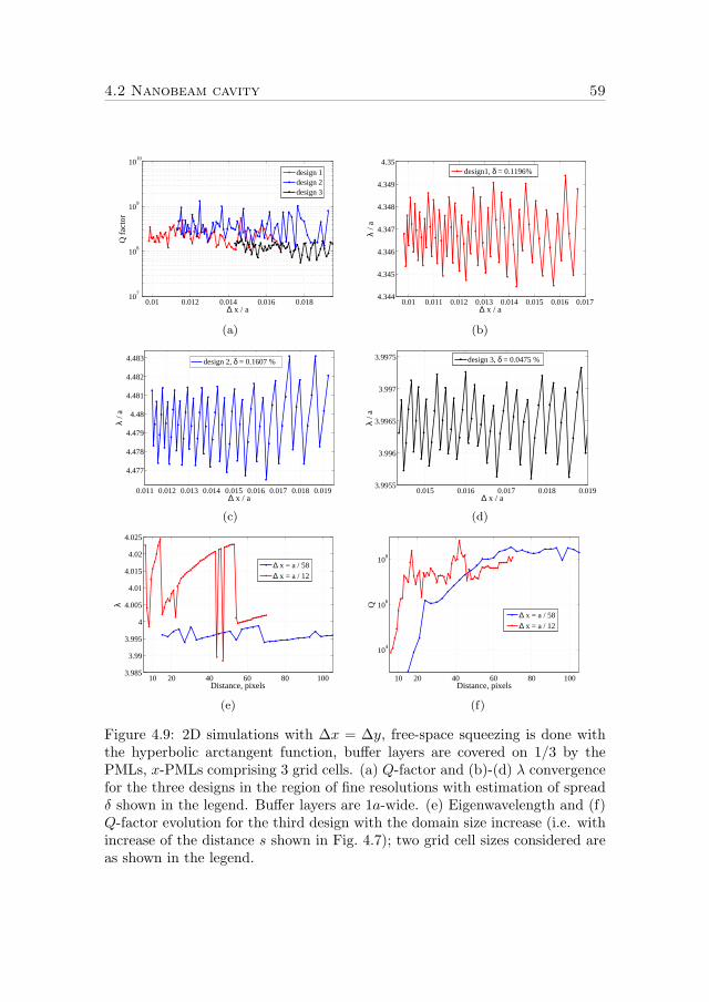
4.2 Nanobeam cavity 59
0.01 0.012 0.014 0.016 0.01810
7
108
109
1010
∆ x / a
Q f
acto
r
design 1design 2design 3
0.01 0.011 0.012 0.013 0.014 0.015 0.016 0.0174.344
4.345
4.346
4.347
4.348
4.349
4.35
∆ x / a
λ / a
design1, δ = 0.1196%
(a) (b)
0.011 0.012 0.013 0.014 0.015 0.016 0.017 0.018 0.019
4.477
4.478
4.479
4.48
4.481
4.482
4.483
∆ x / a
λ / a
design 2, δ = 0.1607 %
0.015 0.016 0.017 0.018 0.0193.9955
3.996
3.9965
3.997
3.9975
∆ x / a
λ / a
design 3, δ = 0.0475 %
(c) (d)
10 20 40 60 80 1003.985
3.99
3.995
4
4.005
4.01
4.015
4.02
4.025
Distance, pixels
λ
∆ x = a / 58∆ x = a / 12
10 20 40 60 80 100
104
106
108
Distance, pixels
Q
∆ x = a / 58∆ x = a / 12
(e) (f)
Figure 4.9: 2D simulations with ∆x = ∆y, free-space squeezing is done withthe hyperbolic arctangent function, buffer layers are covered on 1/3 by thePMLs, x-PMLs comprising 3 grid cells. (a) Q-factor and (b)-(d) λ convergencefor the three designs in the region of fine resolutions with estimation of spreadδ shown in the legend. Buffer layers are 1a-wide. (e) Eigenwavelength and (f)Q-factor evolution for the third design with the domain size increase (i.e. withincrease of the distance s shown in Fig. 4.7); two grid cell sizes considered areas shown in the legend.

60 Ultra-high-Q nanophotonic resonators
Having established that an and dn should vary somehow we investigated sev-eral ways to that. Following the mode-matching approach to high-Q nanobeamcavities [65,152] perforation should consist of two regions: a long periodic partacting as a Bragg reflector and a chirped, mode matched defect region. Sev-eral laws to tailor the nanobeam design have been compared. Among themare 1/ 10
√n multiplier to decrease both an and dn (design 1); cavity formation
similar to [62] when hole diameter and lattice constant vary linearly in the re-ciprocal space (design 2); and linear decrement of an and dn towards the middleof nanobeam [65]. With all mentioned designs we were able to rise the Q-factorto the order of 108 simply by playing with parameters. Table 4.1 summarizedetails of different nanobeam cavity designs. For the first and third designswe start by defining modified hole diameter dn and modified segment size anis calculated afterwards. For the design three calculation of modified latticeconstant an precedes evaluation of the defect hole diameters.
In Fig. 4.8 an example of the Q and λ convergence curves for the designthree is plotted starting from a quite coarse resolution, while Fig. 4.9a–d allowsto do more detailed comparison between different designs in the region of fineresolutions. Special attention to this is required because the convergence ofthe nanobeam cavity is worst than for the membrane resonators, which is seenalready in 2D simulations, Fig. 4.9a. Indeed, 1D PhC basis for the nanobeamcavity somewhat less reflecting than 2D stop band utilized in the membraneresonators. It leads to less Q stability when fabricated nanobeam design or itsfinite difference description has imperfections.
All of the designs from Table 4.1 have similar Q-factor values, Fig. 4.9a,the design three revealing faster convergence than others. In Fig. 4.9b–d theresonance wavelength convergence is plotted for the three designs in the same∆x range as in Fig. 4.9a. To estimate the convergence rate, relative spread∆λ of convergence curves around a central wavelength λ0 can be introduced:δ = ∆λ
λ0100%. The design three has δ one order less than the designs one and
two even at rougher resolutions. Thus we came to the modification according tothe linear law as better converging numerically. The design three will be usedin all further nanobeam cavity simulations with hope that better numericalstability can lead also to better potential stability with respect to the designperturbations.
Figure 4.9e,f elucidates the influence of the domain size on Q and λ calcula-tion. A distance s from the nanobeam frontier to the end of the computationaldomain, see Fig. 4.7, is increased incrementally by adding more grid cells. Redlines correspond to the grid cell of a/12 which clearly gives strongly overesti-mated resonance wavelength in Fig. 4.9e because of too rough discretization.Refining of the sampling (to 58 points per lattice constant a) significantly min-imizes the relative error in λ-evaluation and most interestingly, this error staysthe same irrespective of the actual domain size so that even for as small buffer as15·a/58≃0.26a correct λ-calculation takes place. It means that eigenwavelengthcomputation is not that sensitive to the buffer layers extension as to the choiceof good sampling, what is in agreement with the sphere considerations before.

4.2 Nanobeam cavity 61
0.5 1 1.5 2 2.5 3 3.5 4
3.2
3.4
3.6
3.8
4
4.2
λ / a
Height h / a
0.5 1 1.5 2 2.5 3 3.5 410
0
101
102
103
104
105
106
107
Q
resonance wavelength λquality factor Q
(a) (b)
Figure 4.10: (a) 3D field patterns of the TE mode in the nanobeam cavity ofthe height 0.7a. (b) Resonance wavelength λ and Q-factor dependence on thenanobeam height h. The grid cell is cubic, arctanh-buffer layers are of a sizealong both y and z-directions, a/3 distance goes for the PMLs, x-PMLs are 3cells wide.
Minimal optimal domain size when Q-factor calculation saturates and does notimprove anymore with the domain size prolongation shows up in Fig. 4.9f. Thisminimal domain size, that is already enough for the most accurate Q evaluationat the given meshing, can be estimated as ∼ 12 · a/12 = 58 · a/58 = 1a. Thusfor the nanophotonic cavity we see the direct analogy of the FDFD methodperformance observed before for the simple spherical resonator.
4.2.2 3D modeling
Nanobeam height variation
In the 3D modeling a defect region in the nanobeam cavity is perforated ac-cording to the design three from Table 4.1. Fig. 4.10 shows dropping of theresonance wavelength of the TE-mode in the nanobeam cavity with the reduc-tion of its height h along the third z-direction. Decreasing of the nanobeamheight also greatly minimizes mode volume, so that for the height h = 0.5ait is equal to 0.86 (λ/n)3. We use these nanobeam height in the followingconvergence studies and for the modeling of the coupled cavity structures.
Equidistant mesh, arctanh squeezing function
Figure 4.11 demonstrate the Q and λ convergence for the two domain sizeswhen buffer squeezing function is arctangent based and thus relatively flat, i.e.the grid step is just slowly increased in physical space behind the nanobeamborder. This relatively weak and slow squeezing requires long enough distanceleft from the nanobeam frontier to the PML start. Thus the PMLs occupying

62 Ultra-high-Q nanophotonic resonators
0.06 0.08 0.1 0.12 0.14 0.16
3.18
3.19
3.2
3.21
3.22
3.23
3.24
3.25
Voxel size, a
λ / a
STLwidth = 1aSTLwidth = 1.1amesh aligned
(a)
0.06 0.08 0.1 0.12 0.14 0.16
104
105
106
107
108
Voxel size, a
Q
STLwidth = 1aSTLwidth = 1.1amesh aligned
(b)
Figure 4.11: (a) The resonance wavelength and (b) the Q-factor versus gridcell size for the two STL widths. The PMLs width in x direction is 3 grid cells.

4.2 Nanobeam cavity 63
third part of the buffer is an optimal choice here. The Yee cell is cubic here inthe whole range of voxel sizes.
The resonance wavelength calculation has uncertainty less than 1%. Eval-uation of the resonance wavelength can be improved by using, for example,Hz mesh aligned with respect to the flat nanobeam surfaces. In this case theaveraging procedure does not depend on the finite number of subpixels usedto make polarization-sensitive averaging and finite-difference description of thepermittivity become better what should improve also simulation results. In-deed, when Hz mesh nodes coincide with the slab-air interface (square pointsin Fig. 4.11a, better stability for the λ calculation is achieved, although lesssampling points might be plugged into the mesh-aligned convergence curve.Q-values given by the aligned mesh seems to lie on the nonaligned mesh con-vergence curve close to the average value of λ oscillations.
There is no visible difference between the non-aligned and aligned Q-factorvalues, Fig. 4.11b. In general, precision of the Q computation does not dependsignificantly on a particular grid step and on the averaging procedure used tofind finite-difference array for permittivity. Thus this is reasonable result thataligning of the mesh does not influence the Q-evaluation. The Q convergenceis not that good for both meshes, what is related to 1D-like structure for thenanobeam cavity.
Non-equidistant mesh, x/(1− x) squeezing
Now we consider the steepest squeezing function from Fig. 3.4, which allowsto start the PMLs in the computational space closer than at 2a/3 distancefrom the nanobeam surface for the buffer size being 1a. The PML size of halfthe buffer should improve simulation results because the nanobeam-to-PMLsdistance stays of the same size in physical space as it was with the arctan-gent function before. From Fig. 4.12a we see that the results for λ attainimprovement compared to those in Fig. 4.11, the relative uncertainty in λ isreduced more than twice. The Q-factor evaluation is so unstable that bothFig. 4.11b and Fig. 4.12b show similar convergence behavior. We can remindhere that low accuracy of the Q-factor evaluation reflects high sensitivity ofthe Q-factors of 1D photonic-crystal-based structures to imperfections in theirfinite-difference description. Small perturbations in wavevectors caused by im-perfections strongly effect the efficiency of coupling with leaky modes lyinginside the light cone. Due to the 1D nanobeam geometry this perturbationsare more pronounced than in the case of 2D photonic crystals resonators. Thisleads to considerable variations in the nanobeam cavity Q-factor, whereas res-onance wavelengths remain stable. Nevertheless, the obtained Q-factor valuesgive a reliable order-of-magnitude estimate. The nonuniform mesh (blue curvesin Fig. 4.12) applied along x-direction, ∆y being equal ∆z, greatly reducesmemory requirements and computational time while preserving convergenceproperties similar to uniform mesh for both λ and Q.

64 Ultra-high-Q nanophotonic resonators
0.04 0.06 0.08 0.1 0.12 0.14 0.163.19
3.195
3.2
3.205
3.21
3.215
3.22
3.225
3.23
∆ z / a
λ
x3 stretchno stretch
(a)
0.04 0.06 0.08 0.1 0.12 0.14 0.1610
4
105
106
107
108
∆ z / a
Q
x3 stretchno stretch
(b)
Figure 4.12: (a) The resonance wavelength and (b) Q-factor versus grid stepfor uniform (∆x=∆y=∆z) and nonuniform S3 x-mesh from 4.4. Buffer sizealong y and z directions is 1a-wide with 1/2 occupied by the PMLs, the PMLswidth in x-direction being 3 grid cells.

Chapter 5
Coupled nanobeam cavities
Optical elements based on a coupled system possess rich functionality ow-ing to additional degrees of freedom given by varying displacement of cavi-ties and efficient frequency tuning. Change of coupling strength of the res-onators with their rearrangement addresses the issue of parasitic interactionbetween components which is so important for integrated photonics. Side-coupled nanobeams [77,152,153] offer new possibilities for shaping optical fieldsat nanoscale, which is potentially beneficial for various applications includingtrapping and manipulation of particles [154], sensing and optical switchingthrough optomechanical interactions with suspended nanobeams [63, 64]. Re-alization of flexible control over the mode coupling in arrays of nanocavitieswill also contribute to the development of on-chip quantum-optical interferom-eters [71] and quantum computers [155].
Spectral position of the supermodes formed in two cavities placed side byside can be analyzed with the FDTD technique. The problem is that if severalmodes are traced in the time domain within a single run, the accuracy of theQ-factor determination may degrade, and extraction of the separate mode fieldprofiles requires Fourier transformation of field evolution stored for some spacevolume and time interval. If the two modes are degenerate, separating themone from the other with the FDTD method is even less trivial, especially if atthe degeneracy point the coupled structure does not have a plane of symmetryallowing to split the two modes by the appropriate domain reduction. On thecontrary, the FDFD technique grants an opportunity to get straightforwardly,in one run, the pictures of several modes, their eigenvalues and quality factors.Even when the modes in the coupled cavities are degenerate, we get an ideahow they may look like — though the picture becomes now ambiguous. In thisChapter 5 the FDFD technique is used to analyze single and coupled photoniccrystal nanobeam cavities.

66 Coupled nanobeam cavities
5.1 Two coupled nanobeams
We suggested and show numerically that longitudinal shift in nanobeam cavi-ties significantly alters coupling efficiency between multiple closely packed res-onators. Whereas the concept of longitudinal offset between cavities has beenpreviously developed for dielectric rod arrays at microwave frequencies [156]and micro-scale ring resonators at optical wavelengths [79], we demonstratehere new possibilities for light control at nanoscale. In particular, we showthat for particular values of the longitudinal shift, the cavity modes becomedegenerate irrespective of the transverse shift between nanobeams.
When two identical cavities are positioned parallel to each other, theirmodes undergo hybridization. Supermodes possess symmetric or anti-symmetricprofiles [153] and shift in frequency up and down from the former level. We willrefer to this splitting as frequency detuning. The frequency detuning betweenthe supermodes normally increases as the cavities are brought closer, and suchsensitivity to separation can lead to pronounced optomechanical phenomena.This may have various applications, including mechanically-induced frequencyconversion for optical waves [123]. Analogous effects of modes splitting occurin coupled periodic waveguides, where several channels can enrich the bandstructure of a single mode waveguide in a controllable way, e.g. in slow lightmodes positioning at the band edge on demand.
5.1.1 2D analysis of field profiles
First we analyze two side-coupled nanobeam cavities as in Fig. 5.1a where theright half of the structure is shown (the left half is symmetric). The individualidentical nanobeams has design 3 from Table 4.1. This gives a linearly chirpedarray, while other designs are also possible; the general mode properties areusually similar for different chirp functions. The resonance wavelength of suchsingle nanobeam in 2D is λ = 3.9964a, Q = 1.5·108, Fig 4.8. Two parametersdescribe the position of the second nanobeam cavity relative to the first one:the transverse separation p and the longitudinal shift s, Fig. 5.1a.
To make the computational work efficient all modeling is done at the be-ginning for 2D nanobeam geometries with main emphasis on field patternsredistribution as coupled resonators are rearranged. As we are interested incoupling effects between two nanobeam resonators when they are shifted lon-gitudinally and transversally with respect to each other, we need to performa new computational cycle each time the structure is modified by a small dis-placement. In the 2D case the execution time is several minutes even for hugeresolutions such as ntot = 6 · 105 grid nodes available with a 8Gb station.
Mode profiles in Fig. 5.1b, s = 0, shows formation of the symmetric and an-tisymmetric cavity modes when two nanobeam resonators are brought together.Magnetic field hot spots coincide with the location of holes. At the separationp = 1.5a we see only electric field in the air gap between the nanobeams. Whenone of the nanobeams is subjected to a longitudinal shift the system loses its

5.1 Two coupled nanobeams 67
a9 d8 d1a2
p
s
a
(a)
x
y
a d a d
Figure 5.1: (a) Two nanobeams, each of width t = a, refractive index n = 3.4and drilled with 20 holes in each half, separated one from another by p andshifted longitudinally by s. (b) Field profiles for modes (labeled mode 1 and 2)in coupled cavities with zero, s = 0.3a and s = 0.4a longitudinal shifts whenseparation p = 1.5a, for each shift mode one being positioned at the top whilemode two takes the bottom position.

68 Coupled nanobeam cavities
0 0.2 0.4 0.6 0.8 1
3.99
4
4.01
4.02
λ / a
s / a
0 0.2 0.4 0.6 0.8 110
0
101
102
103
104
105
106
107
108
109
Q f
acto
r
mode 1mode 2
d = 1.5 a
0.6 0.8 1 1.2 1.4 1.6 1.8 23.4
3.8
4.2
4.6
5
5.4
5.8
λ / a
p / a
0.6 0.8 1 1.2 1.4 1.6 1.8 210
0
101
102
103
104
105
106
107
108
109
Q f
acto
rmode 1mode 2
s = 0
(a) (b)
0.6 0.8 1 1.2 1.4 1.6 1.8 2
3.8
3.9
4
4.1
4.2
4.3
4.4
4.5
λ / a
p / a0.6 0.8 1 1.2 1.4 1.6 1.8 2
100
101
102
103
104
105
106
107
108
109
Q f
acto
r
mode 1mode 2
s = 0.3 a
0.6 0.8 1 1.2 1.4 1.6 1.8 2
3.9
4
4.1
4.2
4.3
4.4λ
/ a
p / a
0.6 0.8 1 1.2 1.4 1.6 1.8 210
0
101
102
103
104
105
106
107
108
109
Q f
acto
rmode 1mode 2
s = 0.4 a
(c) (d)
0.6 0.8 1 1.2 1.4 1.6 1.8 23.7
3.8
3.9
4
4.1
4.2
4.3
4.4
λ / a
p / a
0.6 0.8 1 1.2 1.4 1.6 1.8 210
0
101
102
103
104
105
106
107
108
109
Q f
acto
r
mode 1mode 2
s = 0.5 a
0.6 0.8 1 1.2 1.4 1.6 1.8 2
3.6
3.7
3.8
3.9
4
4.1
4.2
4.3
4.4
λ / a
p / a
0.6 0.8 1 1.2 1.4 1.6 1.8 210
0
101
102
103
104
105
106
107
108
109
Q f
acto
rmode 1mode 2
s = 0.6 a
(e) (f)
Figure 5.2: (a) Detuning of the mode one and mode two vs the longitudi-nal shift. Transverse separation between nanobeam axes is p = 1.5a. (b)-(f)Resonance wavelengths and Q-factors of eigenmodes in side-coupled nanobeamcavities vs. their transverse separation p. Results are presented for four dif-ferent shifts: (b) s = 0.0a; (c) 0.3a; (d) 0.4a; (e) 0.5a, (f) 0.6a as indicated bylabels. Separation of 1.0a and less corresponds to a single dielectric beam withtwo rows of holes.
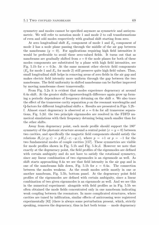
5.1 Two coupled nanobeams 69
symmetry and modes cannot be specified anymore as symmetric and antisym-metric. We will refer to notation mode 1 and mode 2 to call transformationsof even and odd modes respectively with gradual shift starting from zero.
At zero longitudinal shift Ex component of mode 1 and Ey component ofmode 2 has a node plane passing through the middle of the air gap betweenthe nanobeams (y = 0). For applications requiring high field intensities itwould be preferable to avoid these zero-valued fields. It turns out that asnanobeams are gradually shifted from s = 0 the node planes for both of thesemodes components are substituted by a plane with high field intensities, seeFig. 5.1b for s = 0.3a. At the same moment other electric field components(Ey for mode 1 and Ex for mode 2) still preserve quite high field values. Thus,small longitudinal shift helps in removing areas of zero fields in the air gap andmakes electric field intensity more uniform through the gap between the twonanobeams. The field uniformity in shifted nanobeams can be further improvedby moving nanobeams closer transversally.
From Fig. 5.2a it is evident that modes experience degeneracy at around0.4a shift. At the greater shifts eigenwavelength difference again grow up form-ing a periodic dependence of frequency detuning on the shift s. We also tracethe effect of the transverse cavity separation p on the resonant wavelengths andQ-factors for different longitudinal shifts s. Results are presented in Figs. 5.2b–f. Almost exact degeneracy is observed at s = 0.4a for all transverse separa-tions, Fig. 5.2d: the two principle eigenmodes are resolved in the FDFD nu-merical simulations with their frequency detuning being much smaller than forthe other shifts.
Away from degeneracy point, each mode profile should support the 180◦
symmetry of the photonic structure around a central point (x = y = 0) betweentwo cavities, and specifically the magnetic field components should satisfy therelations Hz(x; y; z) = pHz(−x;−y; z), where p = +1 or p = −1 for thetwo fundamental modes of couple cavities [157]. These symmetries are visiblefor mode profiles shown in Fig. 5.1b and Fig. 5.3c,d. However we note thatexactly at the degeneracy point, the field profiles of the eigenmodes are definedwith certain ambiguity and do not have to satisfy the rotational symmetry,since any linear combination of two eigenmodes is an eigenmode as well. Asshift starts approaching 0.4a we see that field intensity in the air gap and inone of the nanobeams falls down, Fig. 5.1b for s = 0.4a. The connectionbetween the modes weakens. As the result modes settle mostly in one oranother nanobeam, Fig. 5.5b, bottom panel. At the degeneracy point fieldprofiles of the eigenmodes are defined with certain ambiguity, since a linearcombination of two given eigenmodes is an eigenmode as well. And we see thisin the numerical experiment: alongside with field profiles as in Fig. 5.5b weoften obtained the mode fields concentrated only in one nanobeam indicatingweak coupling between the resonators. In more complicated structures, wherecavities are tuned by infiltration, similar effects of anticrossing were registeredexperimentally [82] (there is always some perturbation present, which, strictlyspeaking, removes the degeneracy, thus in fact both terms — mode degeneracy

70 Coupled nanobeam cavities
0.6 0.8 1 1.2 1.4 1.6 1.8 20
0.2
0.4
0.6
0.8
1
p / a
|∆ λ
| / a
shift 0 ashift 0.1 ashift 0.3 ashift 0.4 ashift 0.5 ashift 0.6 a
1.6 1.8 2 2.2 2.4 2.610
−4
10−3
10−2
10−1
p / a
|∆ λ
|
s = 0
(a) (b)
(c)
(d)
Figure 5.3: (a) Increase of eigenwavelength difference with shortening oftransversal separation p between the nanobeams, different shifts are printed inthe legend. (b) |∆λ| in logarithmic scale for nonshifted nanobeams. (d) Evo-lution of magnetic field Hz in two slightly shifted nanobeams (s=0.1a) whenclosing the air gap between them, i.e. separation p is reduced from 1.1a to1.05a. (c) Hz field distribution in two connected nanobeams with p = 0.9a ats = 0, s = 0.3a and s = 0.4a shifts.
and anticrossing — can mean the same here).In Fig. 5.3a the eigenwavelength difference is plotted showing the highest
values for non-shifted resonators and significantly smaller |∆λ| for non-zeroshifts. Due to symmetric positioning of 0.3a and 0.5a shift values around thedegeneracy point, the wavelength difference given by these shifts are equal toeach other for nanobeams separated by p > 1.1a. When nanobeams are farenough transversally and coupling strength is small, |∆λ| depends on s byorder law seen in Fig. 5.3b. In Fig. 5.3b for illustration purpose the spectralsplitting for non-shifted nanobeams is plotted in a logarithmic y-scale; the othernonzero shifts, except for the degeneracy point, also give similar straight linesin the |∆λ|-log scale if separation p is big enough to correspond to the weak

5.1 Two coupled nanobeams 71
coupling regime.When the resonators are moved transversally closer so that separation be-
tween them decreases, the interaction between the nanobeams intensifies, andall fields, including magnetic one, spread through the air gap. The picture ofthe mode profiles alters compared to p = 1.5a, see Fig. 5.3c,d. Eigenmode fieldsextend over the whole cavity even when the hole positions in upper and lowercavities are effectively shifted in the out-of-phase configuration, i.e. s = 0.4a.In Fig. 5.3c the evolution of mode 1 at small shift 0.1a is shown when closingthe air gap. Drastic changes occur with the mode 1 profile when connecting thenanobeams: yet very intensive field at p = 1.11a is strongly pushed out fromthe cavity center at p = 1.05a. Thus for nonlinear applications special careshould be paid to the extremely thin slots between the nanobeams. Fig. 5.3dcollects field patterns for both modes at different shifts when air-dielectric in-terfaces are absent and we actually have one cavity consisting of two chirpedarrays. In Fig. 5.3d the mode 1 has quite complicated field distribution ats = 0.3a, however becoming symmetric to the mode 2 field profile at the de-generacy s = 0.4a. Note that although field maps in stitched nanobeams arereally complex they are all 180◦ rotation symmetric relative to the center pointbetween the nanobeams.
5.1.2 3D Q and λ dependence on the longitudinal shift
In 3D we consider the same nanobeam design from Fig. 5.1a and discussmore the development of the Q and λ curves with the rearrangement of thenanobeams. The 3D Q-factor of a single nanobeam cavity is around 4 ·106 andthe operating wavelength λ = 3.21a for the TE mode, Fig. 4.12. To achievefine sampling in 3D problems symmetry domain reduction is applied were itis possible to satisfy memory requirements. The system of two nanobeam res-onators with a longitudinal shift loses plane-reflection symmetry and the wholedomain should be considered so benefits of stretched meshes is fully used here.Discretization in the cavity center is set to 0.05a − 0.1a with sparser meshin the rest of the structure. 3D Q-factor computations are done on a 48Gbstation with the maximum execution time approaching 2 hours per single run.Correct averaging is an important issue in 3D simulation where that fine res-olution as in 2D cannot be achieved. As p → 1 a unit Yee cell might containtwo boundaries from two closely spaced nanobeams and the averaging shouldbe done only once taking into account both boundaries simultaneously.
Moving nanobeams closer to each other leads to stronger coupling and pro-nounced increase of the eigenwavelength difference between the doublet of su-permodes, see Fig. 5.4a. At p = a the system is changed abruptly as the gapbetween the two nanobeams disappears, so the structure consists now of a sin-gle high-dielectric bar with two parallel rows of holes in it. That explains acharacteristic peak in the wavelength dependence of the mode eigenfrequencyplotted in Fig. 5.4a. Mode 1 (even) has higher wavelength than mode 2 (odd)for the whole range of separations p as can be easily seen from a simple per-

72 Coupled nanobeam cavities
0.6 0.8 1 1.2 1.4 1.6 1.8 22.8
3
3.2
3.4
3.6
3.8
4λ
/ a
p / a
0.6 0.8 1 1.2 1.4 1.6 1.8 2
101
102
103
104
105
106
107
Q
mode 1mode 2
(a)
0 0.2 0.4 0.6 0.8 1
3.22
3.23
3.24
3.25
3.26
3.27
λ / a
s / a
100
101
102
103
104
105
106
107
Q
mode 1mode 2, p=1.2amode 1mode 2, p=1.5a
(b)
Figure 5.4: Tuning of resonance wavelengths of coupled modes by (a) changingseparation between non-shifted (s = 0) nanobeams; (b) changing the longitu-dinal shift s for two separations (p = 1.2a and p = 1.5a as indicated by labels).Right axis shows the 3D Q-factor values.
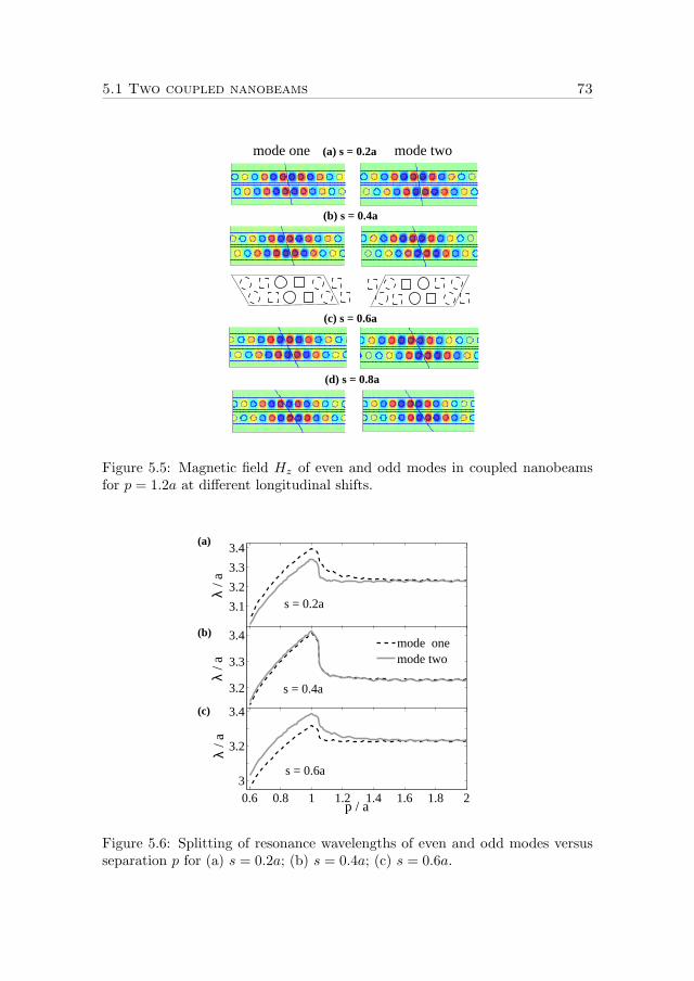
5.1 Two coupled nanobeams 73
mode one mode two
(b) s = 0.4a
(c) s = 0.6a
(d) s = 0.8a
(a) s = 0.2a
Figure 5.5: Magnetic field Hz of even and odd modes in coupled nanobeamsfor p = 1.2a at different longitudinal shifts.
3.1
3.2
3.3
3.4
λ / a
3.2
3.3
3.4
λ / a
mode onemode two
0.6 0.8 1 1.2 1.4 1.6 1.8 23
3.2
3.4
λ / a
p / a
s = 0.2a
s = 0.4a
s = 0.6a
(a)
(b)
(c)
Figure 5.6: Splitting of resonance wavelengths of even and odd modes versusseparation p for (a) s = 0.2a; (b) s = 0.4a; (c) s = 0.6a.

74 Coupled nanobeam cavities
turbation theory [158]. When the gap between nanobeams is closed and they-dimension is further reduced, the effective refractive index of the system andhence the eigenwavelengths are also decreased [41]. Remarkably, when varyingthe separation no significant variation in the Q-factor is seen. The Q-factorvalue is close to 106 for both even and odd modes, see Fig. 5.4a.
Now we analyze the effect of the longitudinal shift s. In Fig. 5.4b thewavelengths and Q-factors of the fundamental eigenmodes vs. shift s for sep-arations p = 1.2a and p = 1.5a are plotted. As the shift starts growing fromzero, mode detuning is reduced and, independent on separation p, the modesbecome degenerate at around s ≃ 0.4a what is in contrast to resonators withunmodified lattice constant [156] where the degeneracy shift was exactly 0.5aindependent on rod radii variation. Thus this is primarily variation of latticeconstant that is responsible for the specific value of the degeneracy shift. Notethat 0.4a ≃ 0.5a6, i.e. the shift at degeneracy point is approximately equal tohalf the average lattice constant in the cavity region.
In Fig. 5.5b for s = 0.4a we plot another picture at the degeneracy com-pared to Fig. 5.1b with the magnetic field nodes in one nanobeam opposing fieldlobes in another. These degenerate modes can be schematically sketched withdiagrams in Fig. 5.5b. Standing wave profiles with slow spatial decay from thecenter of the cavity towards the periphery allow neglecting low-intensity outerregions and then central parts of the patterns are identical upon reflection,making the occurrence of the degeneracy point (geometrically, central parts ofthe defect regions for the two modes also satisfy reflection-symmetry if chirpedhole diameters approximated to be the same in the middle). Had mode pro-files less gradual changes in the succession of field minima and maxima alongthe nanobeams (as shown by bold circles and squares in the diagrams), theformation of the degeneracy would be hardly possible.
For the shifts larger than s = 0.4a the mode detuning is increased, reachinga maximum at around s ≃ 0.8a where eigenwavelength difference approachesthe same value as at s = 0. The revival of coupling at s ≃ 0.8a is again due tothe gradually chirped nanobeam design and field profiles extended along thenanobeams. Thus mode detuning depends on the shift almost periodically, andthe cavity modes 1 and 2 are adiabatically transformed as the parameter s isvaried from 0 to a, see Fig. 5.5d where it is shown that mode 1 and 2 exchangetheir parity going from s = 0 to s = 0.8. Most important, the Q-factor valuesremain of the same order of magnitude as for a single cavity.
In Fig. 5.6 we compare the eigenmodes wavelength dependencies on separa-tion p for three longitudinal shifts s = 0.2a, 0.4a, 0.6a. The upper panel showsthe reduced spectral detuning of the modes for the intermediate shift s = 0.2a.The plot in Fig. 5.6b shows that for non-overlapping nanobeams the modes arealmost exactly degenerate at s = 0.4a for any transverse separation p. Afterthe degeneracy point, at s = 0.6a modes 1 and 2 swap their wavelengths.
By comparing Fig. 5.2 against Figs. 5.4 and 5.6 we see that 2D and 3Dsimulations give essentially similar dependencies for λ andQ on the longitudinalshift s and transversal separation p of the cavities, indicating the possibility to

5.2 Three coupled nanobeams 75
design coupled nanobeam cavity systems in 2D successfully. This is because thephysics of coupling of dielectric nanobeam cavities is relatively simpler than,for example, the coupling of metallic split-ring resonators where essentiallythree-dimensional interplay of magnetic and electric excitations is important.
5.2 Three coupled nanobeams
In multiple side-coupled nanobeam cavities the modes can also be tuned by lon-gitudinal shifts with the degeneracy observed at certain shift. Degeneration ofmodes in structures containing many elements amounts to the absence of para-sitic coupling between the neighboring units. Instead of increasing the distancebetween optical components usually used to minimize cross-talk, longitudinalshift can be proposed to create dense photonic integrated circuit. Moreover, byappropriate choice of transversal separation the degeneracy wavelength of cou-pled nanobeams (up to three resonators in our tests) can be tuned to a singlenanobeam resonance wavelength. This potentially allows adjacent waveguidingcomponents, all together, and each separately, to operate at the same wave-length. For example, compact single-wavelength switch matrix can be createdon the basis of a nanobeam-switcher with nonlinearity [150]. Another fieldof application is building an array of nanobeam cavities to form a quantumoptical network where many identical resonators should be placed closely oneto another on a chip [155]. Additionally, by controlling the mode coupling itbecomes possible to tailor the optical field across an array of multiple nanocav-ities for applications in particle trapping [154] and tailored optomechanicalinteractions [63,64].
5.2.1 Weak coupling regime
We did 2D simulations (letting the nanocavities be infinitely high) to catch ba-sic features of mode tunability. For three side-coupled nanobeam cavities theirrelative alignment can be characterized by separations p2, p3 and longitudinalshifts s2, s3 of the second and third cavities. As an example we consider equallyspaced (p2 = p3 = p) nanobeam cavities, only the middle one being shifted:s2 = s, s3 = 0. The dependence of mode wavelength detuning (relative to asingle cavity) on the shift s is given in Fig. 5.7a for p = 2.3a. We observebehavior similar to the case of two nanobeams. Specifically, all three modesbecome degenerate at s ≃ 0.4a; by varying p we can control the wavelength ofthe degenerate modes, and it coincides with the wavelength of a single cavity,Fig. 5.7a. Mode profiles for non-shifted system (s = 0) are shown in Fig. 5.7b.Note that mode 3 is localized at the outer cavities, so its wavelength is notsensitive to the middle cavity shift as observed in Fig. 5.7a. There is a nicemechanical analogy with modes of three weakly coupled pendulums: in mode 1,all three pendulums are swinging in phase; in mode 2, two outward pendulumsmove forward while the middle one moves backward; in mode 3, the central

76 Coupled nanobeam cavities
0 0.2 0.4 0.6 0.8 1
-1
-0.5
0
0.5
1
1.5x 10
-3
/ a
s / a0 0.2 0.4 0.6 0.8 1
101
103
105
107
109
Q
mode 1
mode 2
mode 3
mode 3mode 1 mode 2
λ
(a)
(c)
(b)
Δ
Figure 5.7: Modes in three side-coupled nanobeam cavities with transversaldisplacement between the neighboring nanobeams being equal to 2.3a. Themiddle nanowire is longitudinally shifted, the other two being kept stationary.(a) Spectral detuning of the three modes from the single nanobeam cavitywavelength λ = 3.9965a. Right y-axis—theQ-factor of the three coupled modes(for an isolated nanobeam cavity, Q = 1.5 · 108). Hz profiles for the modes inthe three (b) unshifted and shifted by (c) 0.41a nanobeams.
pendulum is at rest and two others are moving oppositely.
At the degeneracy point (s ≃ 0.4a) the eigenmode profiles can be primarilylocalized at individual cavities, see Fig. 5.7c. In Fig. 5.7c the mode profiles ats = 0.41a reveal complete vanishing of field in neighboring nanobeams whereasfor two coupled nanobeams shift of s = 0.4a was more likeable to be called theexact degeneracy shift value. In fact, it is quite difficult to detect precise valueof the degeneracy as it requires extremely fine step in s and long simulationtimes; besides, accuracy of computation is also limited by the finite-differencedescription. However small deviations from the exact degeneracy does not

5.2 Three coupled nanobeams 77
change field mapping significantly as solutions to Maxwell’s equations are allsmooth functions.
Wavelength detuning is much less pronounced at p = 2.3a than at p = 1.5a,p = 1.2a considered previously. The reason to choose the separation p =2.3a is that coupling between the nanobeams is already weak and the energysplitting becomes symmetric relative to the initial energy level as follows fromthe standard perturbation approach. And the degeneracy wavelength of anarray of nanobeams is the same as the isolated nanobeam eigenwavelength(this is not true for the case of strong coupling at p = 1.5a).
Although we are in the weak coupling regime, spectral splitting correspond-ing to p = 2.3a is about 0.2%, which for telecom wavelength 1.5µm amountsto 3 nm spread in wavelength. A comparable shift in resonance wavelengthis induced by inclusion of nonlinearity in the nanobeam; this allows cavityoperation as a switcher totally transmitting or suppressing the signal depend-ing on turning on/off the nonlinearity [150]. Thus 0.2% energy difference formultiple nanobems placed at p = 2.3a on a photonic integrated chip intro-duces parasitic coupling hindering single-wavelength operation. The distance1.3a between nanobeam edges (corresponding to p = 2.3a) is not that large interms of interaction between the cavities.
If we further suppose the core of nanobeam cavity is nonlinear (e.g. takinginto account refractive index increase due to nonlinearity), then the degeneratemodes in the array of nonlinear cavities can be also tuned to a single resonatorwavelength by p variation. A single-wavelength operating switching array canbe build on the basis of such nanobeam cavities that will work equally well forsingle- or multiple-channel excitation applied. (In the case of the single-cavitynonlinear operation based on 0.03% change in refractive index, the frequencyshift due to presence of neighboring ‘passive’ nanobeams is estimated to bearound a negligible 2 · 10−4%).
We have verified that mode degeneracy also occurs in four side-to-side cou-pled nanobeam cavities. Thus we expect mode degeneracy in multiple side-coupled cavities when they have staggered longitudinal shifts, such that neigh-boring nanowires are shifted longitudinally by s ≃ 0.4a. We also expect thatthe Q-factor in multi-cavity structure should remain of the same order of mag-nitude as that of a single nanocavity.
5.2.2 Strong coupling regime
Strong coupling regime is investigated by doing 3D simulations with symmetryplanes being enforced through the domain reduction. For the three nanobeamsdependence of mode detuning on a shift s of a middle nanobeam is given inFig. 5.8a for p = 1.2a. Here three modes become degenerate at s ≃ 0.4a withwavelength λ ≃ 3.235a bigger than the isolated 3D nanobeam eigenwavelength3.21a. 3D Q-factors for three coupled cavities are found to remain of the sameorder as the longitudinal shift is varied, see Fig. 5.8a.
Mode profiles for non-shifted system (s = 0) are shown in Fig. 5.8b. When

78 Coupled nanobeam cavities
0 0.2 0.4 0.6 0.8 13.21
3.23
3.25
3.27
3.29
s / a0 0.2 0.4 0.6 0.8 1
101
102
103
104
105
106
107
Q
mode 1
mode 2
mode 3
(a)
mode 1 mode 2 mode 3(b)
(c)
Figure 5.8: Modes in three side-coupled nanobeam cavities. The middlenanobeam is longitudinally shifted, the other two being kept stationary. Trans-verse separation between the neighboring nanobeams is p = 2.3a. (a) λ andQ of the three modes. (b) Hz profiles for the modes in the three non-shiftednanobeams. (c) Hz profiles of the degenerate modes at s = 0.4a.
symmetry planes are enforced the eigenmode profiles at the degeneracy point(s ≃ 0.4a) look as in Fig. 5.8c. In general, in the degeneracy point wepresent the results of our numerical calculations based on the direct solutionof Maxwell’s equations and without taking linear combinations with data ob-tained. Our calculations for two and three nanobeams gave two variants offield maps at the degeneracy: 180◦ rotational (2 resonators) or reflection (3 res-onators) symmetrical pictures, and profiles with field localization at individualresonators. Simulations enforcing PEC/PMC planes for the three nanobemasgive degenerate modes strictly reflection-symmetrical; however we can guessthat these pictures do not help in understanding physical reality better thando profiles with field localization in individual nanobeams implying completevanishing of interaction between the cavities. And it is that characteristicdegeneracy profile with field extinction in one of the cavities that is clearly
5.2 Three coupled nanobeams 79
predominant in all 2D and 3D simulations for all range of separations and thatshould be more expectable in the experiments than other linear combinationof the degenerate mode profiles.
In summary, we have shown that a longitudinal shift between side-couplednanocavities enables flexible control of eigenmodes including the realization ofexact degeneracy, a feature impossible in non-shifted resonators. The qual-ity factor of coupled nanobeam cavities stays close to that of a single cavity,indicating good practical prospects for such structures.


Chapter 6
Metallic gratings
Metals exhibit a plethora of optical phenomena associated with their rich dis-persion properties, and are widely used in the range from visible to GHz fre-quencies. Incorporating frequency-dependent permittivity for numerical mod-eling in the time domain is not trivial: auxiliary variables are to be introducedto account for dispersion, making transient-wave simulation of metals morecomplicated and memory-consuming compared to modeling of dielectric ma-terials. Besides, time domain methods are bound to analytical description ofmaterial parameters while real-life metal permittivity might deviate signifi-cantly from that given by Drude or Drude-Lorentz expressions, so that usingtabulated dispersion values becomes desirable. Finally, modeling inclined lightincidence on periodic structures (gratings) is not straightforward in the timedomain, and many nontrivial tricks have been proposed to work around thatdifficulty [119]. On the contrary, in the frequency domain no complicationsarise with introduction of metal dispersion, so the code preserves its same formfor all types of media, and no difficulties occur for plane waves impinging onperiodic structure at an arbitrary angle.
Metal-dielectric composites are intensively investigated in the optical do-main, and many methods are adapted to consider various metallic geometries:from strictly analytical through hybrid semi-analytical to fully numerical finite-difference solutions. At the technologically important THz frequencies nanos-tructured metals started to gain attention only recently. At extremely longwavelengths, frequency domain methods are expected to perform better thantheir time domain counterparts, Fig. 1.8, and in this section an emphasis is on anumerically challenging task of simulating field enhancement in single and mul-tiple (periodic) slits in thin subwavelength films when the ratio of the gratingperiod to the slit width reaches extremely high values of 104. In this chapter wecalculate energy transmission, reflection and absorption of gold slabs withoutor with perforation. At low frequencies the permittivity of gold can be definedby Eq. (1.16) with ϵ∞ = 1, plasma frequency ωp = 1.37×10⁴ THz and γ = 40.7THz [159].

82 Metallic gratings
6.1 Planar metallic slab at THz frequencies
6.1.1 Analytic solution
10−2
10−1
100
101
102
0.993
0.994
0.995
0.996
0.997
0.998
0.999
1
Frequency, THz
|r|
10−2
10−1
100
101
102120
140
160
180
φ
AmplitudePhase
10−2
10−1
100
101
102
0.98
0.985
0.99
0.995
1
Frequency, THz
R
h = 20 nmh = 30 nmh = 40 nmh = 50 nmh = 60 nmh = 70 nmh = 80 nmh = 90 nmh = 100 nm
(a) (b)
10−2
10−1
100
101
102
10−6
10−5
10−4
10−3
10−2
Frequency, THz
T
10−2
10−1
100
101
102
2
4
6
8
10
12
14x 10
−3
Frequency, THz
A
(c) (d)
Figure 6.1: (a) Amplitude and phase of reflection at a single gold-dielectricinterface; (b) reflectance, (c) transmittance and (d) absorption of gold slabs ofdifferent thickness h placed freely in the air.
Let us consider a plane subwavelength film in the THz range. Transmission,reflection and absorption of metal slab can be found through standard Fresnel’sformulas with the complex permittivity of metal. The amplitude coefficient ofreflection from a single interface at normal incidence is
r =n1 − n2
n1 + n2, (6.1)
where n1,2 are the refractive indices of two media. From Eq. (6.1) we seethat no matter from which side radiation is incident upon the boundary, theamplitude of reflected wave is the same but the phase is inverted (−1 = eiπ). Ina symmetric metal-dielectric sandwich, we have equal amplitudes of reflectionfrom both interfaces. Figure 6.1a shows that at low frequencies single metal-dielectric interface has very high amplitude of reflection and phase shift about πin the whole range from 10−2 up to 102 THz. Due to this half-period phase shift,electric field vector has the same amplitude but opposite sign upon reflection;

6.1 Planar metallic slab at THz frequencies 83
thus boundary conditions at the frontier of PEC and dielectric are satisfiedstrictly so that the radiation virtually does not enter the PEC-like metal.
We see no significant variation in reflectivity with frequency for subwave-length 20–100 nm slabs in Fig. 6.1b what is in line with Fig. 6.1a where coef-ficient of reflection at a single metal-dielectric interface is almost constant inthe whole range of frequencies. No sign of interference effects is expected withincreasing film thickness above 100 nm: they will be strongly suppressed dueto such a high imaginary part of refractive index at low frequencies [160].
Even for very thin 20-nm-thick films reflectance stays very high while trans-mittance is suppressed, Fig. 6.1b,c. Taking into account that h = 20nm isdeeply below the skin depth which is about 300–800 nm at THz (and increasesvery fast approaching ω → 0), metal behavior similar to PEC having infiniteconductivity and total reflectance irrespective of slab width is clearly seen.Utilization of skin depth at low frequencies to estimate tunneling through thinfilms in the same way as it is usually done at visible should be done withcare. Thickness of the film should be deeply below the skin depth, just a fewnanometers, for any noticeable transmission to be observed at THz.
In the visible part of spectrum the effect that very thin layers of metal can bemore absorptive than bulk pieces is well known for metal-coated nanoparticles,which are intensively used in photovoltaics as providing higher absorbance thansolid metal ellipsoids [92]. It turns out that not only in condition of plasmonexcitation small quantities of metal can more intensively absorb radiation thanbulk metal pieces: the absorption increase with reduction of slab thickness isseen in Fig. 6.1d.
Let’s summarize our discussion. Huge real and imaginary parts of metalpermittivity at low frequencies make perfect electric conductor description ofmetal nearly an ideal approximation. At THz frequencies a negligible partof radiation impinging on the metal penetrates inside. A small portion ofTHz wave energy passed inside the metal decays spatially slow due to skindepth increased by several times at low frequencies compared to the visible.It amounts to lower absorption per unit length experienced by non-uniformTHz wave inside the metal whereas at higher frequencies significant amountof radiation tunnels effectively through the subwavelength films and can beabsorbed at a higher rate. Thus at THz frequencies a 20–100 nm thick gold filmbecomes non-transparent and reflects most of radiation incident on it whereas,for example, 20 nm film under visible illumination can transmit up to 50% oflight. Metal is indispensable material for THz range in this sense because, forexample, VO2 films of the same thickness experience only a 20% change intheir transmission after dramatic change of refractive index from 1 to 10000due to phase transition [161]. The ability of metal to effectively govern long-wavelength radiation on the length scale of nanometers with low absorption isof good use when we are interested in strong field concentration in air gaps inmetals without sacrificing transmission.
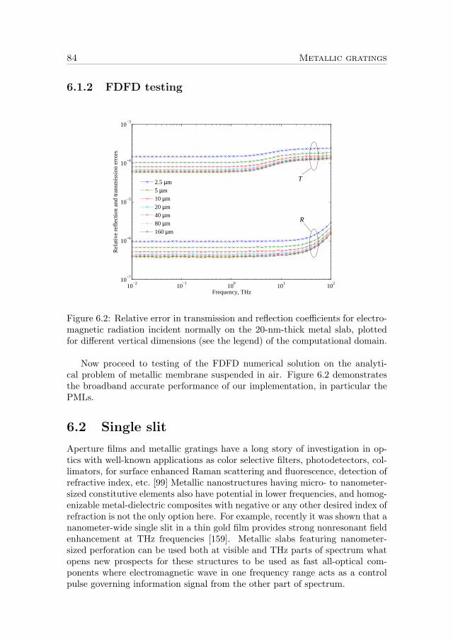
84 Metallic gratings
6.1.2 FDFD testing
10−2
10−1
100
101
102
10−7
10−6
10−5
10−4
10−3
Frequency, THz
Rel
ativ
e re
flect
ion
and
tran
smis
sion
err
ors
2.5 µm5 µm10 µm20 µm40 µm80 µm160 µm
T
R
Figure 6.2: Relative error in transmission and reflection coefficients for electro-magnetic radiation incident normally on the 20-nm-thick metal slab, plottedfor different vertical dimensions (see the legend) of the computational domain.
Now proceed to testing of the FDFD numerical solution on the analyti-cal problem of metallic membrane suspended in air. Figure 6.2 demonstratesthe broadband accurate performance of our implementation, in particular thePMLs.
6.2 Single slit
Aperture films and metallic gratings have a long story of investigation in op-tics with well-known applications as color selective filters, photodetectors, col-limators, for surface enhanced Raman scattering and fluorescence, detection ofrefractive index, etc. [99] Metallic nanostructures having micro- to nanometer-sized constitutive elements also have potential in lower frequencies, and homog-enizable metal-dielectric composites with negative or any other desired index ofrefraction is not the only option here. For example, recently it was shown that ananometer-wide single slit in a thin gold film provides strong nonresonant fieldenhancement at THz frequencies [159]. Metallic slabs featuring nanometer-sized perforation can be used both at visible and THz parts of spectrum whatopens new prospects for these structures to be used as fast all-optical com-ponents where electromagnetic wave in one frequency range acts as a controlpulse governing information signal from the other part of spectrum.

6.2 Single slit 85
Transmission through single slits in metallic films can be strongly enhanceddue to resonance effects, like cavity resonances [89,90,162–164] when thicknessof metal film or slit width satisfy Fabry-Perot conditions. One of importantaspects of these resonance effects is strong light concentration in air slits [89]that might be directly used for nonlinear applications [25]. Specially designedcharge and current reservoirs can be employed for further increase of field in-tensities [165] where field enhancement up to 60 were achieved in the visiblepart of spectrum.
At THz frequencies [166] where metal behaves as PEC, enhancement dueto cavity resonance effects was reported to reach the value of 430 [167]. Sur-prisingly high field enhancements of about 103 and higher are accumulatedinside slits [159] in the regime when they act as tiny capacitors at low frequen-cies [168]. This regime is of particular interest in the rest of this Chapter 6.Due to capacitor model it is easier to find some laws for enhancement whereasdependencies for transmittance that does not have direct analogue in statics issomewhat more complicated to establish so the main issue is enhancement lawfor a single and periodic slit.
The p-polarized (i.e., electric field lies in the xy plane in the insert inFig. 6.3) fundamental mode in the slit exists in the whole range of frequen-cies and thus field enhancement is possible at THz frequencies, whereas s-
10−6
10−4
10−2
100
102
100
102
104
106
108
1010
f, Thz
Enh
ance
men
t
w = 20 nmh = 10:100nm
wh
fxz
y
Figure 6.3: Enhancement in an isolated slit cut in slabs of different thicknesstaking values from 10 to 100 nm. The insert shows the geometry of the problem:single slit of width w in a gold slab of thickness h illuminated by p-polarizedplane wave of frequency f . The center of coordinates lies in the center of theslit.

86 Metallic gratings
polarization has cut-off wavelength and at low frequencies light do not passthrough the slit [99]. Here and later by enhancement we will understand theamplitude of electric field averaged over the central line of the slit (if the slit issymmetric and the film is sandwiched symmetrically, then only Ex componentcontributes to the enhancement thus defined) and normalized to the amplitudeE0 of incident radiation:
enhancement =⟨Ex⟩slit |y=0
E0=
∫wEx |y=0 dx
wE0(6.2)
This averaged Ex amplitude does not necessarily coincide with the field valuein the very center of the slit, the difference being bigger for wider slits.
6.2.1 1/f law for enhancement
We start from an isolated slit and investigate the dependence of enhancementon the slit width w and frequency f , and we compare this with the behavior ofmultiple slits later in this chapter. In Refs. [159,168] it was shown theoreticallyand experimentally that single slit exhibits the 1/f law for the field enhance-ment. This rule follows from a capacitor model in which field enhancement isdirectly proportional to the total charge accumulated on the slit edges. Thus1/f is immediately obtained as with wavelength λ growing, the larger part ofmetal is involved in gathering electrons near slit edges.
The question that now we are interested in is how good the capacitor modeland the 1/f law is, and how the enhancement depends on slab thickness and slitwidth in some reasonable bounds, i.e. before entering the regime of pronouncedresonance behavior. We are also concerned with numerical method at hand:how high the enhancement can go while moving towards lower frequencies.
Figure 6.3 shows excellent fulfilment of 1/f law in a broad range of fre-quencies; achievement of extremely high enhancements of 108 deeply belowTHz range, that is at MHz frequencies; and independence of the enhancementon slab thickness. In the paper [168] the authors observe some dropping ofenhancement with increase of the slab width, however their enhancement isdefined as a field in the center of quite large slit of 200 nm width at fixedwavelength what might explain these discrepancies in calculations.
In Fig. 6.3 at shorter wavelengths we can notice a slight spread in thedevelopment of the 1/f curves for slabs of various heights. At higher frequenciespossible stronger deviation from 1/f law is related to shifting towards region offaster electromagnetic wave oscillations: static capacitor approximation breaksbecause slit dimensions become comparable to the wavelength. Thus at thefrequency above 102 THz some influence of slab thickness on the enhancementmight take place.
We established that enhancement is almost independent on film thicknesswhen it is much less then the wavelength of light, and that capacitor modeltogether with the FDFD method apparently have no limits in calculating verylarge field intensities in extra-narrow slits at low frequencies.
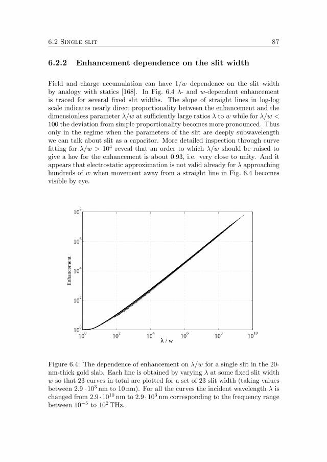
6.2 Single slit 87
6.2.2 Enhancement dependence on the slit width
Field and charge accumulation can have 1/w dependence on the slit widthby analogy with statics [168]. In Fig. 6.4 λ- and w-dependent enhancementis traced for several fixed slit widths. The slope of straight lines in log-logscale indicates nearly direct proportionality between the enhancement and thedimensionless parameter λ/w at sufficiently large ratios λ to w while for λ/w <100 the deviation from simple proportionality becomes more pronounced. Thusonly in the regime when the parameters of the slit are deeply subwavelengthwe can talk about slit as a capacitor. More detailed inspection through curvefitting for λ/w > 104 reveal that an order to which λ/w should be raised togive a law for the enhancement is about 0.93, i.e. very close to unity. And itappears that electrostatic approximation is not valid already for λ approachinghundreds of w when movement away from a straight line in Fig. 6.4 becomesvisible by eye.
100
102
104
106
108
1010
100
102
104
106
108
λ / w
Enh
ance
men
t
Figure 6.4: The dependence of enhancement on λ/w for a single slit in the 20-nm-thick gold slab. Each line is obtained by varying λ at some fixed slit widthw so that 23 curves in total are plotted for a set of 23 slit width (taking valuesbetween 2.9 · 103 nm to 10 nm). For all the curves the incident wavelength λ ischanged from 2.9 ·1010 nm to 2.9 ·103 nm corresponding to the frequency rangebetween 10−5 to 102 THz.

88 Metallic gratings
Simulation details
For simulations of an isolated slit the buffer layers along the y-direction startright after the slab boundary and are squeezed with the x/(1 − x) function,Fig. 3.4, to computational size of 2–3µm, to include more vortices of electro-magnetic field around the slab, Fig. 1.4. One third of the total size of thesqueeze transform layers is covered by PMLs. The same buffers are used alsofor the x-direction where squeezing layers include metallic plates and squeezingstarts right after the slit edges. Grid steps near the slit are around 0.1–0.4 nm,being gradually stretched to reach 20 times of that for the rest of the structure,Fig. 6.5.
6.3 Periodic slits in metal film
Under condition of resonance excitation the transmission of light through per-forated slab can be strongly prohibited [19] or, vice versa, enhanced, the formerfeature underpinning a well-known extraordinary optical transmission (EOT)phenomenon [95]. It turns out that for the lossless model of metal, for ex-ample the PEC model, by cutting neighboring slits around a single slit thetransmission increases with increasing the number of slits, and infinite periodicstructure can exhibit total transmission [88].
−20 −10 0 10 20−20
−15
−10
−5
0
5
10
15
20
Y−coordinate
X−
coor
dina
te
Figure 6.5: Refinement of the mesh near the metal-slit boundaries.

6.3 Periodic slits in metal film 89
(a) (b)
Figure 6.6: (a) Periodic grating of period P formed in gold film of thicknessh = 20nm by perforating slits of width w. (b) Metal grating placed into staticelectric field; only top semi-space is shown, with external filed E0 = Einf beingunperturbed at infinity.
For a non-resonant case intuitive considerations let us assume that if thelight is tunneled through a single slit at a certain wavelength, adding more slitsmight lead to higher transmittance. But what will be with the field enhance-ment in the slits? Will periodic structure be able to achieve the same extremelyhigh intensities in its slits as an isolated slit does? From the capacitor modelfor a single slit we can estimate that the period P required to provide one ofthe slits in a periodic structure with charges to give the same capacitance as anisolated slit should be about or bigger than the wavelength of light [167]. Butexactly at P = λ we have a condition for Fano resonance, which is already outof our interest. Thus we can expect that at λ < P condition the enhancementin the periodic structure will not exceed an isolated slit value.
In this section we consider the field enhancement in lamellar metallic grat-ings in the wavelength range when λ ≫ h and λ > P and investigate the appli-cability of electrostatic approximation to propagating electromagnetic waves.Static model gives us a simple rule for electric field inside a slit as a ratio ofgrating period to slit width, P/w, relative to the amplitude of incident wave.It turns out that this rule can be satisfied quite generally for periodically per-forated metal films starting from zero up to THz frequencies unless the gratingperiod or film thickness becomes close to the wavelength of light, i.e. we stepin the regime where resonance effects appear. In general, evolution of curves inthe plots throughout this Chapter 6 is traced up till the first Rayleigh-Woodanomaly, i.e. till λ = P . Applicability of static model also implies total energytransfer from upper to lower half-space and thus total transmission not avail-able in single apertures. Adding of periodic openings to metal membrane candrastically change its transmission from zero to one, what can be utilized forswitching [161].
By doing numerical simulation we explore field enhancements up to 104 ina 10 nm air gap in periodic structures in 0–0.1THz range. The combination ofcontrollable field concentration given by simple law together with total trans-mission, both available in a broad range of frequencies, paves the way for usage

90 Metallic gratings
of metallic gratings for improvement of THz sources, detectors and sensors,as wavelength-independent polarizers and essentially for molecular absorptionspectroscopy [169,170].
6.3.1 10-nm-wide slit in gratings of different periods
Electrostatic model
As we are interested in translation of electrostatic solution to our case of tran-sient incident fields, the width of the slab is chosen to be quite thin, i.e.h = 20nm everywhere in the Section 6.3. The geometry of a periodic grat-ing is shown in Fig. 6.6a, whereas Fig. 6.6b illustrates static variant of theproblem: metallic grating placed into the infinite homogeneous electric field.Let us consider this static version first. Knowing that work done by electricforces to move a test charge along closed contour in a potential field gives zerowe can use this to find field in the slit by integrating along the red line inFig. 6.6b. Periodicity requires that the field on the two red lines perpendicularto the slab spaced by P has the same vector values, what nullifies total con-tribution of the forces along these lines. From the rest two lines, one passingthrough the middle of the slab, the other one along the homogeneous field atinfinity, the enhancement is derived as:
PE0 − w ⟨Ex⟩slit = 0 (6.3a)
⟨Ex⟩slit =P
wE0 (6.3b)
Thus enhancement in periodic structures depends on the period of the gratingand the size of the opening while slab thickness does not play any role inquasistatic regime. Recalling now about single slit that can be considered inFig. 6.6b with a limiting case P → ∞ we find out that independence of singleslit enhancement on the height of the slab h is a reasonable and quite expectedbehavior.
Flat enhancement
Concluding the static model, we expect to have some regime where transmit-tance will be unity and enhancement will obey Eq. (6.3) as follows from thestatic limit. Let see how this agrees with the precise numerical calculations. InFig. 6.7 the enhancement and transmittance are plotted for gratings of varyingperiod P = (2 : 1 : 10) · 101:1:4 when slit width is fixed to 10 nm. Fig. 6.7ashows that there exist broad frequency range for each of considered periodswhere static model conclusions work perfectly well. Enhancement equality toP/w is fulfilled with high precision for any P/w from 2 up to extreme 104.
Threshold frequency for exiting flat enhancement region is connected withreaching λ = P condition. Quick dropping of enhancement curves near theirends in Fig. 6.7a signalizes about entering the region of asymmetric Fano res-onance shape. For example, the period corresponding to the enhancement 10

6.3 Periodic slits in metal film 91
10−2
10−1
100
101
102
100
101
102
103
104
f, THz
Enh
ance
men
t
2000
200
20
w = 10 nm h = 20 nm
a)
10−2
10−1
100
101
102
0
0.2
0.4
0.6
0.8
1
f, THz
T
w = 10 nm h = 20 nm
202002000
b)
Figure 6.7: (a) Field enhancement and (b) transmittance of a 10-nm-wide slitscut in a 20-nm-thick film versus frequency for different grating periods P . Theenhancements in quasi-static limit are chosen to be ⟨Ex⟩slit /E0 = (2 : 1 :10) · 101:1:3, the corresponding period of grating is P = w ⟨Ex⟩slit /E0.
92 Metallic gratings
is P = 10 · w = 100 nm what gives Rayleigh-Wood condition λ = P translat-ing to fR−W ∼ 103 THz and approximately one frequency order, from 102 to103 THz, takes for the enhancement to vanish completely. From Fig. 6.7b wenotice that threshold condition for transmittance is more severe, i.e. transmis-sion dropping starts two frequency orders before the Rayleigh-Wood condition.In another example with very large enhancement of 2·103, fR−W ∼ 101 THzand again roughly one order less, i.e. at 1THz, enhancement plateau regimebreaks, the transmittance starting decreasing at a much smaller frequency of10−1 THz.
Thus by appropriate choice of geometry parameters the region with somedesired enhancement and transmittance of unity can be selected. In such azone with flat enhancement, THz pulses of short duration can be fully trans-mitted with all their spectral constituents experiencing the same enhancementin the near field of the gratings. As regards extremely high enhancements,for that periodic structures require very long periods and narrow slits. Formany applications demanding strong field, like change of refractive index dueto nonlinearity, high transmission is inessential and can be sacrificed in favorof extended frequency range of high field intensities.
Comparison with a single-slit film
The question which system, an isolated slit or a periodic grating, can proposehigher field concentrations is addressed by plotting enhancement curve for asingle slit of width w = 10nm with a red line in Fig. 6.7a. As it was expected,at a fixed frequency periodic structure in general cannot accumulate biggercharge and stronger field than an isolated slit. We see an amazing correlationin behavior of the two systems: an envelope formed by enhancements in periodicstructures almost coincide with single slit curve. It appears that for periodicstructure we have two regimes of operation: λ ≪ P is in deep electrostaticapproximation with total transmission and flat enhancement zone obeying P/wratio when all slits work cooperatively; if λ → P cooperative action of slitssplits and each slit interacts with light rather as a separate scatterer so thatthe enhancement in multiple slits follows the curve for isolated-slit structure.In fact even in the second regime we can anticipate that periodic grating canstill preserve some coherent interaction between neighboring slits as envelopein blue color in Fig. 6.7a lies slightly higher then the red line.
In general, at a fixed incident wavelength, single or periodic apertures witha given opening width give the same highest possible enhancement and additionof more perforations with certain periodicity to a single slit can improve onlytotal transmission.
Threshold frequency
In general, the frequency f0 at which zone of flat enhancement ends can beapproximately found from intersection of P/w horizontal with (λ/w)0.93÷1 line
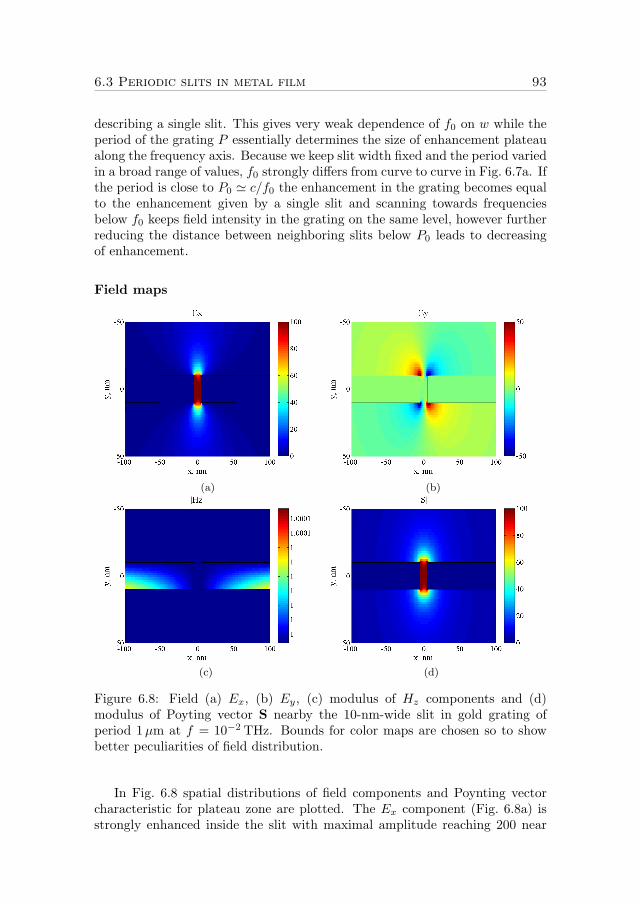
6.3 Periodic slits in metal film 93
describing a single slit. This gives very weak dependence of f0 on w while theperiod of the grating P essentially determines the size of enhancement plateaualong the frequency axis. Because we keep slit width fixed and the period variedin a broad range of values, f0 strongly differs from curve to curve in Fig. 6.7a. Ifthe period is close to P0 ≃ c/f0 the enhancement in the grating becomes equalto the enhancement given by a single slit and scanning towards frequenciesbelow f0 keeps field intensity in the grating on the same level, however furtherreducing the distance between neighboring slits below P0 leads to decreasingof enhancement.
Field maps
(a) (b)
(c) (d)
Figure 6.8: Field (a) Ex, (b) Ey, (c) modulus of Hz components and (d)modulus of Poyting vector S nearby the 10-nm-wide slit in gold grating ofperiod 1µm at f = 10−2 THz. Bounds for color maps are chosen so to showbetter peculiarities of field distribution.
In Fig. 6.8 spatial distributions of field components and Poynting vectorcharacteristic for plateau zone are plotted. The Ex component (Fig. 6.8a) isstrongly enhanced inside the slit with maximal amplitude reaching 200 near

94 Metallic gratings
the slit sharp edges. The Ey component (Fig. 6.8b) has a node at x = 0 planeand antisymmetric field distribution around the node plane with strong con-centration at metal corners. From intensity maps for electric components andPoyting vector it is seen that radiation couples inside the slit mainly throughmetallic corners. Thus the wave upon incidence on the slit passes through quiteessential spatial transformations in the near field of the slit before being fullytransmitted to the far field zone.
By looking at the Hz component (Fig. 6.8c) we see that magnetic field al-most does not participate in electromagnetic field shaping process; its unit valuethrough all the domain means that Sx = Ey ·Hz ≃ Ey and Sy = −Ex ·Hz ≃−Ex thus intensity maps for Poynting vector components look similar to theelectric field distributions. As seen from Fig. 6.8d, the Sy component prevailsin total energy flow so that |S| looks very similar to Ex field distribution.
Simulation details
For periodic gratings in the same way as for a single slit, stretching of the finite-difference mesh reaches a ratio of 20 in most of simulations. When calculatingextra-narrow slits, e.g. w = 10nm considered in this section, integration ofthe field along the air gap was substituted by a point value of the field in thevery center of the aperture. This is fully justified as the field along centralline appears to be highly uniform in narrow slits, however grid points lying atthe slit edges with zero Ex amplitude should not be included into the integral.Avoiding inclusion of such points while integrating is difficult to automate asjust a few points come on the aperture.
As in the case of FDFD application to PhC resonators where calculation ofQ and λ gave the best convergence on computational domains organized in twodifferent ways, i.e. in the first case for better quality factor accuracy, largerdomain is used even if resolution is coarse and in the second case for eigenwave-length calculations, good sampling is more important than actual domain size;for metal gratings similar different approaches can be used for calculations oftransmission and enhancement. As pointed out in introduction, vortices andevanescent tails of electromagnetic field spread far away around the grating,thus correct reconstruction of energy flow and correct simulation of transmis-sion relies heavily on big enough computational domain. In our transmittancecalculations the air buffer superposed with space squeezing were taken around2 to 10 µm, the biggest size being utilized for extremely high enhancementsgenerating strong evanescent fields. At the same moment calculations of en-hancement are based on fine discretization and the domain can be reducedfurther down to 1.5µm in favor of sub-nanometer grid step in the region ofmetal-dielectric frontiers and hot spots of electromagnetic energy.

6.3 Periodic slits in metal film 95
10−2
10−1
100
101
0
200
400
600
800
1000
f, THz
Enh
ance
men
t
50
P = 20000 nm h = 20 nm
(a)
10−2
10−1
100
101
0
0.2
0.4
0.6
0.8
1
f, THz
T
50
P = 20000 nm h = 20 nm
(b)
Figure 6.9: (a) Enhancement and (b) transmittance in gratings from Fig. 6.6awith unchangeable periodicity 20µm but with alternation of slit width accord-ing to the following approximate set of numbers: [400 200 100 67 50 40 33 2925 22 20] which correspondingly give enhancements [50 100:100:1000] withinthe plateau zone.

96 Metallic gratings
6.3.2 Changing slit width when the period is fixed
In previous Section 6.3.1 we considered extra-narrow slit and going further wewould like to know whether the same flat enhancement behavior holds for widerapertures. Let us now fix gold grating period P = 20µm and scan over differentaperture widths; because P is always kept constant Rayleigh-Wood anomaly isexpected at the same frequency for different slit widths. Fig. 6.9 demonstratesthat electrostatic approximation with enhancement given by P/w again worksvery well for broad range of slit widths, besides our additional calculationsrevealed that even for very wide apertures with w = 10µm the enhancementfactor of 2 is stably obtained. As in previous Fig. 6.7, here for narrow slits theend of enhancement plateau appears roughly one frequency order before theλ = P condition, with transmission falling down one more order earlier.
Threshold frequency
For strong field focusing, slit width should preferably be chosen quite smallwith the period reaching dozens or hundreds of µm what additionally weakensthe dependence of f0 on w as compared to its dependence on P . In Fig. 6.9threshold frequency only slightly changes from curve to curve, especially forsmallest widths, in contrast to Fig. 6.7 which gives an argument for prevailinginfluence of P on threshold frequency. Thus if higher enhancement is requiredwithout significant reduction of plateau size, it should be better done throughdecrease of aperture size but not the period increase.
−150 −100 −50 0 50 100 1500
50
100
150
200
x, nm
Ex
w = 200nm, P = 2⋅104nm
w = 100nm, P = 1⋅104nm
w = 10.0nm, P = 1⋅103nm
Figure 6.10: Profiles of electric field component Ex, all giving enhancements of100, as calculated by averaging inside the slit along the y = 0 line. Parametersof different gratings giving the same enhancement are shown in the legend.

6.3 Periodic slits in metal film 97
2 4 6 8 10 12 140
50
100
150
200
250
300
f, THz
Enh
ance
men
t
w = 400nmw = 200nmw = 100nmw = 50.0nmw = 28.6nm
100
101
101
102
f, THz
Enh
ance
men
t
w = 400nmw = 200nmw = 100nmw = 50.0nmw = 28.6nm
(a) (b)
Figure 6.11: Detalization of several curves from Fig. 6.9a with linear scale (a)and logarithmic scale (b) for the enhancement, lines with circles correspond tothe isolated slit and are plotted for the comparison.
Field profiles for different slit width
To know the distribution of Ex field component along the middle line of theaperture, Fig. 6.10 compares three slit widths providing the same enhancementof one hundred calculated via Eq. 6.3. Only in the case of extremely narrow10-nm-wide slit we see really uniform field, while opening of aperture leads todropping of field amplitude well below the value of 100 in the central regionof the slit. Thus small apertures are advantageous not only as effective energyconcentrators but also for creation of uniform field.
Comparison with a single-slit film
In Fig. 6.7 the alignment of envelopes given by single and coupled slits ofdifferent periods were obtained. In Fig. 6.11 we have a closer look at thetransition region from the flat enhancement to the Rayleigh-Wood anomaly. Atfirst glance on Fig. 6.11a, similar behavior of the two systems can be suggested;however when plotted in log-log scale, different laws for the enhancement clearlyshow up. Though passing in close proximity to each other, the enhancementcurves for isolated and periodic slits are governed by essentially different laws.The enhancement in grating is higher in transition frequency region what canbe explained by some constructive interaction of coupled slits with each other.
Discussion
The results shown in this chapter for aperture films can be reproduced byemploying the PEC model for metal instead of gold. Because of no dispersionin the PEC permittivity model and because we are interested in comparingisolated and coupled slit systems, use of w-normalized λ, h, P and a figuresimilar to Fig. 6.7 would be enough for complete analysis. However, both

98 Metallic gratings
Figs. 6.9 and 6.7 are useful for illustrative purpose so real units were preferredto dimensionless ones in our analysis.
As it was mentioned, s-polarized incident wave has cutoff wavelength andat low frequencies its transmission is strongly suppressed. However, additionalcuts perpendicular to the slit can drastically change s-wave transmission [171]what makes current research also relevant for polarization other than p. Thus,the enhancement induced by s-polarized light might also be possible whenmetal film is perforated in a special way.
Additionally to the static model used to explain flat enhancement, we donot completely exclude the possibility that some plasmonic effects contributeto the enhancement in slits of metal gratings at long wavelengths. AlthoughZenneck waves, i.e. SPPs at f → 0, are difficult to excite and detect exper-imentally [172], SPPs dispersion relation lies in close proximity to the lightline at low frequencies, and coupling of incident radiation with electron exci-tation in perforated films is possible. Also, PEC model was shown to emulateplasmonic behavior: surface bound modes [99] or in other terminology spoofplasmons [173] were shown to contribute to the EOT phenomena in perforatedPEC films. Because metal at long wavelengths can be described as nothing butdispersionless perfect conductor, condition for excitation of some surface boundmodes is the same in the wide range of frequencies giving flat enhancement.

Chapter 7
Conclusion
This thesis presents the development of the finite-difference frequency-domain(FDFD) method for rigorous numerical modeling of three-dimensional nanopho-tonic structures. Simulation examples presented include the eigenfrequency andthe Q-factor analysis of a very-high-Q photonic-crystal membrane cavity, a sin-gle and coupled nanobeam resonators, and modeling of light passing throughultra-narrow slits in subwavelength metal films. Of physical significance arethe following results:
(A) Coupled modes of two nanobeam cavities placed side-by-side appear tohave pronounced frequency dependence on their positioning (the longitudinalshift and transversal separation), while the Q-factor of the coupled modes pre-serves the same order of magnitude as that of a single nanobeam. Frequencydetuning of coupled modes depends nontrivially on the longitudinal shift ofcavities, in particular the modes become degenerate for a certain shift. Atthis shift of about half the averaged lattice constant in the defect region, themagnetic field nodes in one nanobeam oppose the field lobes in the other. Thedegeneracy occurs for a broad range of separations between two or multipleside-coupled cavities.
(B) Lamellar metal gratings in extremely subwavelength regime exhibit to-tal transmission of incident p-polarized radiation and strong electric field en-hancement in the nanometer sized slits. With very high accuracy the enhance-ment equals the ratio of the grating period to the slit width, independent of thewavelength and of metal thickness if they are smaller than the wavelength ofincident light. The frequency range of flat enhancement is limited by the first-order Rayleigh-Wood anomaly condition. With the period approaching butnot equal to the incident wavelength, enhancement in slits of periodic gratingsbecomes close to that exhibited by an isolated slit.
For getting reliable Q-factors of nanophotonic resonators or transmissioncharacteristics of metal-dielectric gratings, we addressed the minimum thick-ness of free space buffer layers; the possibility to further squeeze those bufferlayers onto a tighter computational domain; and the nonuniform meshing

100 Conclusion
within the structure. We found that:(I) For a given eigenmode in an open cavity a reasonable estimate for the
optimal cavity-to-PML distance (in physical space) is λ/n — the ratio betweenthe (expected) wavelength λ of that eigenmode and the refractive index contrastn between cavity material and the surrounding medium. This λ/n rule-of-thumb is convenient to use for automated construction of absorbing bufferlayers in the finite-difference or finite-element based software.
(II) To further squeeze the cavity-to-PML distance in the computationaldomain, the xcomp = xphys/(1 + xphys) mapping can be used. With the PMLscovering one half of the squeezed-space buffer layer (the cavity-to-PML distancein physical coordinates thus being equal to the total squeezed-space buffer sizein the computational space) and comprising at least 5 grid cell sublayers, thisgives robust and efficient absorbing buffers for the finite-difference simulations.
(III) Building an orthogonal, nonuniform grid of continuously varying den-sity retains stable convergence for both λ and Q-factor in the eigenmode cal-culations, and reliable transmission and reflection coefficients when modelingextremely subwavelength metal gratings while saving computer memory andcalculation time a lot. Grids with the ratios in the step size reaching 1:10 andmore were investigated.
Applying these findings to real-life modeling leads to considerable com-putation time and memory savings. For example, squeezing the outer freespace reduces the computational domain size, roughly, twofold along each ofthe squeezed coordinates. For metal-dielectric structures, nonuniform grid isessential to describe material interfaces, especially sharp metal edges and fieldsingularities around them, more precisely. For ultra-high-Q photonic-crystalcavities, at a quite coarse sampling of 30 pixels per λ in the region of high fieldintensity, the error in the eigenwavelength is well below 0.5% and the Q-factororder of magnitude can easily be obtained on a laptop computer with 4Gb ofRAM and 2.2GHz CPU frequency in about 5 to 10 minutes.

Appendix A
Fourier transformation
A.1 Continuous Fourier transformation
Let us start from the continuous Fourier transformation (FT). Frequency spec-trum of a mode in a fixed point is given by the Fourier transformation of atime-dependent signal:
A(ω) =
∫ +∞
0
A0e−ω0t
2Q e−iω0te−iωtdt =
∫ +∞
0
y(t)dt (A.1)
For a signal represented by a complex value we will get well known lorentzian.However, if the signal is written as purely real then its FT differs from lorentzian.In Table A.1 there are examples of FT of different signals: complex and real(with different starting phase φ0) according to [174]. In Fig. A.1 we check thedifference in normalized on maximum FT of these signals and find that it isinsignificant was expected. However note, that there are still small differencein position of peaks for |fcos|2 and |fsin|2. Besides, lorentzian fitting by leastsquare procedures in MatLab (lsqcurvefit) and Mathematica (FindFit, Nonlin-earFit) is very dependent and sensitive to number of points involved and guess
function FTyexp(t < 0) = 0yexp(t > 0) = eiω0te−at fexp(ω) =
1i(ω−ω0)+a
ycos(t < 0) = 0
ycos(t > 0) = cos(ω0t)e−at fcos(ω) =
a(a2+ω2+ω20)−iω(a2+ω2−ω2
0)
(a2+ω20−ω2)2+4a2ω2
ysin(t < 0) = 0ysin(t > 0) = sin(ω0t)e
−at fsin(ω) =ω0
(a2+ω20−ω2)+i2aω
Table A.1: Fourier transformation of some signals [174].

102 Fourier transformation
0.2 0.4 0.6 0.8 1 1.2 1.4 1.6 1.80
0.2
0.4
0.6
0.8
1
ω/ω0
Nor
mal
ized
sig
nal i
nten
sity
|f
exp(ω)|2
|fsin
(ω)|2
|fcos
(ω)|2
0.95 1 1.050.75
0.8
0.85
0.9
0.95
1
Figure A.1: Normalized to the maximum squared absolute values of functionsin the right column of table A.1.
parameters to make fit. This simple consideration supports the fact that it iscommon to talk about approximate value of the Q-factor.
A.2 Discrete Fourier transformation
The discrete Fourier transformation (DFT) is defined as follows:
f(ωk) =N−1∑n=0
y(tn)e−iωktn , k = 0, 1, 2, ..., N − 1 (A.2)
where y(tn) discretized with step ∆t, total signal length in time domain is N∆t,f(ωn) - signal in the frequency domain after DFT of signal, step in frequency2π/Nδt. Then frequency points are defined as
ωk = k2π
Nδt, k = 0, 1, 2, ..., N − 1 (A.3)
In Mathematica Eq. A.3 can be used to find resonance frequency, while inMatlab frequency sampling is shifted on one step backwards, i.e. DFT andinverse DFT are initially summed starting from unity in Eq. A.2. Then thefrequency points in Matlab are:
ωk = (k − 1)2π
Nδt, k = 1, 2, ..., N (A.4)

Appendix B
Fabry-Perot resonator:FEM versus FDFDperformance
The eigenwavelength of a rectangular metallic cavity of the lateral size a and bcan be written as:
λ =2√
(ma )2 + (nb )
2(B.1)
FEM is a direct competitor of the FDFD technique. We compare results ofthe 2D in-house Fortran-based FEM and Matlab-based FDFD methods in Ta-ble B.1 for a = b = 10 where a quarter of the cavity (of size 5×5) is discretizedwith quite rough resolution of 19×19 rectangular cells in both cases, Fig. B.1a.The iterative procedure to find eigenvalues is home-made with maximal num-ber of iteration being fixed to 500; the iteration cycle finishes before reaching500 loops if norma of the eigenvalues difference between current and previousiteration is less or equal to the residual 10−12.
From the Table B.1 we see that convergence rate (i.e. maximal number ofiterations) for both methods are similar. The FDFD mistake for the first fun-damental modes is found to be twice larger than that for the FEM calculations,however for modes of higher orders FDFD and FEM performance become sim-ilar. The home-made formulation of the FEM gives discrepancy between theeigenvalues of the degenerate modes (commercial software Ansoft [175] doesnot have this problem; in general it gives relative errors comparable with ourhome-made FEM realization) while the FDFD degenerate eigenvalues coincidewith accuracy up to 5th digit. FEM-solution time is longer because of ne-cessity of many-loops cycles to operate with each element when doing matrixmultiplication to solve generalized eigenvalue problem.

104 Fabry-Perot resonator: FEM versus FDFD performance
(a)
[19x19]
elements
[19x19]
Yee cells
(l,m) analytic
λ
FEM/
error %
iterations/
residual
FDFD/
error %
iterations/
residual
1 (1,1) 14.1421 14.1447 18 14.1460 18
0.0179 4.7*10-13 0.0270 5.3*10-13
2 (1,3) 6.3246 6.3158 500 6.3386 45
-0.1381 1.6*10-12 0.2220 6.2*10-13
3 (3,1) 6.3246 6.3099 79 6.3386 101
-0.2325 1.0*10-12 0.2220 6.9*10-13
4 (3,3) 4.7140 4.7044 75 4.7255 78
-0.2056 6.9*10-13 0.2437 7.2*10-13
5 (1,5) 3.9223 3.8996 500 3.9480 94
-0.5804 6.1*10-12 0.6538 9.7*10-13
6 (5,1) 3.9223 3.8957 169 3.9480 213
-0.6777 8.5*10-13 0.6538 9.4*10-13
(b)
Figure B.1: (a) Field for the first (left) and degenerate second (middle) andthird (right) modes in a quarter of the metallic cavity. (b) Table comparing res-onance wavelength and relative errors given by the FEM and FDFD approachesas well as total number of iterations and residuals at the last iteration.
Bibliography
[1] E. Ozbay, “Plasmonics: merging photonics and electronics at nanoscaledimensions,” Science, vol. 311, pp. 189–193, 2006.
[2] S. A. Ramakrishna, “Physics of negative refractive index materials,” Re-ports on Progress in Physics, vol. 68, pp. 449–521, 2005.
[3] D. K. Gramotnev and S. Bozhevolnyi, “Plasmonics beyond the diffractionlimit,” Nature Photonics, vol. 4, pp. 83–91, 2009.
[4] J. Zhao, P. Belov, and Y. Hao, “Subwavelength internal imagine by meansof a wire medium,” Journal of Optics A: Pure and Applied Optics, vol. 11,p. 075101, 2009.
[5] N. Kundtz and D. R. Smith, “Extreme-angle broadband metamateriallens,” Nature Materials, vol. 9, pp. 129–132, Feb. 2010.
[6] X. Zhang, “Electromagnetic waves in 2d photonic crystals,” MaterialsToday, vol. 12, pp. 44–51, 2009.
[7] I. M. Vellekoop, A. Lagendijk, and A. P. Mosk, “Exploiting disorder forperfect focusing,” Nature Photonics, vol. 4, no. February, pp. 320–322,2010.
[8] J. Valentine, J. Li, T. Zentgraf, G. Bartal, and X. Zhang, “An opticalcloak made of dielectrics,” Nature Materials, vol. 8, pp. 568–571, July2009.
[9] J. Zhang, Y. Luo, and N. A. Mortensen, “Minimizing the scattering of anonmagnetic cloak,” Applied Physics Letters, vol. 96, p. 113511, 2010.
[10] L. H. Gabrielli, J. Cardenas, C. B. Poitras, and M. Lipson, “Silicon nanos-tructure cloak operating at optical frequencies,” Nature, vol. 3, pp. 461–463, July 2009.
[11] X. Chen, Y. Luo, J. Zhang, K. Jiang, J. B. Pendry, and S. Zhang,“Macroscopic invisibility cloaking of visible light,” Nature Communica-tions, vol. 2, pp. 1–6, Feb. 2011.

106 BIBLIOGRAPHY
[12] M. Paniccia and N. Photonics, “Integrating silicon photonics,” NaturePhotonics, vol. 4, pp. 498–499, Aug. 2010.
[13] H.-W. Hubers, “Terahertz technology: Towards THz integrated photon-ics,” Nature Photonics, vol. 4, pp. 503–504, Aug. 2010.
[14] M. Ferrera, Y. Park, L. Razzari, B. E. Little, S. T. Chu, R. Morandotti,D. J. Moss, and J. Azana, “On-chip CMOS-compatible all-optical inte-grator,” Nature Communications, vol. 1, pp. 1–5, June 2010.
[15] D. Weinstein and S. A. Bhave, “The resonant body transistor,” NanoLetters, vol. 10, pp. 1234–1237, Apr. 2010.
[16] C. C. Bof Bufon, J. D. Cojal Gonzalez, D. J. Thurmer, D. Grimm,M. Bauer, and O. G. Schmidt, “Self-assembled ultra-compact energy stor-age elements based on hybrid nanomembranes,” Nano Letters, vol. 10,pp. 2506–2510, June 2010.
[17] J. Leuthold, C. Koos, and W. Freude, “Nonlinear silicon photonics,”Nature Photonics, vol. 4, pp. 535–544, July 2010.
[18] G. Robb, “Nanophotonics: free electrons get light out of a hole,” NatureNanotechnology, vol. 4, pp. 707–708, Nov. 2009.
[19] S. Xiao, V. P. Drachev, A. V. Kildishev, X. Ni, U. K. Chettiar, H.-K.Yuan, and V. M. Shalaev, “Loss-free and active optical negative-indexmetamaterials,” Nature, vol. 466, pp. 735–738, Aug. 2010.
[20] H.-T. Chen, W. J. Padilla, M. J. Cich, A. K. Azad, R. D. Averitt, andA. J. Taylor, “A metamaterial solid-state terahertz phase modulator,”Nature Photonics, vol. 3, pp. 148–151, 2009.
[21] G. T. Reed, G. Mashanovich, F. Y. Gardes, and D. J. Thomson, “Siliconoptical modulators,” Nature Photonics, vol. 4, pp. 518–526, July 2010.
[22] F. Lopez-Tejeiro, S. G. Rodrigo, L. Martin-Moreno, F. J. Garcia-Vidal,E. Devaux, T. W. Ebbesen, J. R. Krenn, I. Radko, S. I. Bozhevolnyi,M. U. Gonzalez, J. C. Weber, and A. Dereux, “Efficient unidirectionalnanoslit couplers for surface plasmons,” Nature Physics, vol. 3, pp. 324–328, 2007.
[23] T. Kosako, Y. Kadoya, and H. F. Hofmann, “Directional control of lightby a nano-optical Yagi Uda antenna,” Nature Photonics, vol. 4, pp. 312–315, March 2010.
[24] S. Mingaleev, A. Miroshnichenko, Y. Kivshar, and K. Busch, “All-opticalswitching, bistability, and slow-light transmission in photonic crystalwaveguide-resonator structures,” Physical Review E, vol. 74, p. 046603,Oct. 2006.

BIBLIOGRAPHY 107
[25] S. Carretero-Palacios, A. Minovich, D. N. Neshev, Y. S. Kivshar, F. J.Garcia-Vidal, L. Martin-Moreno, and S. G. Rodrigo, “Optical switchingin metal-slit arrays on nonlinear dielectric substrates,” Optics Letters,vol. 35, pp. 4211–4213, Dec. 2010.
[26] A. J. Shields, “Semiconductor quantum light sources,” Nature Photonics,vol. 1, pp. 215–223, Apr. 2007.
[27] A. Fratalocchi, “Mode-locked lasers: Light condensation,” Nature Pho-tonics, vol. 4, pp. 502–503, Aug. 2010.
[28] D. Liang and J. E. Bowers, “Recent progress in lasers on silicon,” NaturePhotonics, vol. 4, pp. 511–517, July 2010.
[29] P. Q. Liu, A. J. Hoffman, M. D. Escarra, K. J. Franz, J. B. Khurgin,Y. Dikmelik, X. Wang, J.-y. Fan, and C. F. Gmachl, “Highly power-efficient quantum cascade lasers,” Nature Photonics, vol. 4, no. February,pp. 262–265, 2010.
[30] H. J. Caulfield and S. Dolev, “Why future supercomputing requires op-tics,” Nature Photonics, vol. 4, pp. 261–263, May 2010.
[31] A. H. J. Yang, S. D. Moore, B. S. Schmidt, M. Klug, M. Lipson, andD. Erickson, “Optical manipulation of nanoparticles and biomolecules insubwavelength slot waveguides,” Nature, vol. 457, pp. 71–75, 2009.
[32] M. Celebrano, P. Kukura, A. Renn, and V. Sandoghdar, “Single-moleculeimaging by optical absorption,” Nature Photonics, pp. 95–98, January2011.
[33] J. Zhu, C.-M. Hsu, Z. Yu, S. Fan, and Y. Cui, “Nanodome solar cellswith efficient light management and self-cleaning,” Nano Letters, vol. 10,pp. 1979–1984, June 2010.
[34] A. P. Kulkarni, K. M. Noone, K. Munechika, S. R. Guyer, and D. S. Gin-ger, “Plasmon-enhanced charge carrier generation in organic photovoltaicfilms using silver nanoprisms,” Nano Letters, vol. 10, pp. 1501–1505, Apr.2010.
[35] D. Graham-Rowe, “Solar-powered lasers,” Nature Photonics, vol. 4,pp. 64–65, Feb. 2010.
[36] D. Cyranoski, “Seeing the light,” Nature, vol. 94, p. 726, 2003.
[37] N. Horiuchi, “Light-emitting diodes: Natural white light,” Nature Pho-tonics, vol. 4, p. 738, November 2010.
[38] J. C. Knight, “Photonic crystal fibres,” Nature, vol. 424, pp. 847–851,Aug. 2003.

108 BIBLIOGRAPHY
[39] O. Graydon, “Biophotonics: Fluidic camera aids surgery,” Nature Pho-tonics, vol. 4, p. 585, Sept. 2010.
[40] N. I. Smith, “Biophotonics: A light to move the heart,” Nature Photonics,vol. 4, pp. 587–589, Sept. 2010.
[41] J. D. Joannopoulos, S. G. Johnson, J. N. Winn, and R. D. Meade, Pho-tonic Crystals: Molding the Flow of Light. Princeton Univ. Press, 2001.
[42] K. Hennessy, a. Badolato, M. Winger, D. Gerace, M. Atature, S. Gulde,S. Falt, E. L. Hu, and a. Imamoglu, “Quantum nature of a stronglycoupled single quantum dot-cavity system,” Nature, vol. 445, pp. 896–899, Feb. 2007.
[43] V. Rao and S. Hughes, “Single quantum dot spontaneous emission in afinite-size photonic crystal waveguide: Proposal for an efficient chip singlephoton gun,” Physical Review Letters, vol. 99, p. 193901, Nov. 2007.
[44] T. Yoshie, A. Scherer, J. Hendrickson, G. Khitrova, H. M. Gibbs, G. Rup-per, C. Ell, O. B. Shchekin, and D. G. Deppe, “Vacuum Rabi splittingwith a single quantum dot in a photonic crystal nanocavity,” Nature,vol. 432, pp. 9–12, November 2004.
[45] J. D. Jackson, Classical Electrodynamics. Englewood Cliffs: John Wiley& Sons Inc., 3d ed., 1999.
[46] H. A. Haus, Waves and Fields in Optoelectronics. Englewood Cliffs, NewJersey: Prentice-Hall Inc., 1984.
[47] H. A. Sakoda, Optical Propeties of Photonic Crystals. Germany:Springer, 2001.
[48] J. M. Gerard and B. Gayral, “InAs quantum dots: articial atoms forsolid-state cavity-quantum electrodynamics,” Physica E, vol. 9, pp. 131–139, 2001.
[49] B.-S. Song, S.-W. Jeon, and S. Noda, “Symmetrically glass-clad pho-tonic crystal nanocavities with ultrahigh quality factors,” Optics Letters,vol. 36, pp. 91–93, Jan. 2011.
[50] K. J. Vahala, “Optical microcavities,” Nature, vol. 424, pp. 839–846, Aug.2003.
[51] S. Noda, M. Fujita, and T. Asano, “Spontaneous-emission control byphotonic crystals and nanocavities,” Nature Photonics, vol. 1, pp. 449–458, Aug. 2007.
[52] K. Aoki, D. Guimard, M. Nishioka, M. Nomura, S. Iwamoto, andY. Arakawa, “Coupling of quantum-dot light emission with a three-dimensional photonic-crystal nanocavity,” Nature Photonics, vol. 2,pp. 688–692, Oct. 2008.

BIBLIOGRAPHY 109
[53] Y. Zhang, M. W. McCutcheon, I. B. Burgess, and M. Loncar, “Ultra-high-Q TE/TM dual-polarized photonic crystal nanocavities,” OpticsLetters, vol. 34, pp. 2694–2696, Sept. 2009.
[54] B.-S. Song, S. Noda, T. Asano, and Y. Akahane, “Ultra-high-Q photonicdouble-heterostructure nanocavity,” Nature Materials, vol. 4, pp. 207–210, Feb. 2005.
[55] Z. Zhang and M. Qiu, “Small-volume waveguide-section high Q microcav-ities in 2D photonic crystal slabs,” Optics Express, vol. 12, pp. 3988–3995,Aug. 2004.
[56] O. Painter, J. Vuckovic, and A. Scherer, “Defect modes of a two-dimensional photonic crystal in an optically thin dielectric slab,” Journalof the Optical Society of America B, vol. 16, pp. 275–285, Feb. 1999.
[57] Z. Zhang and M. Qiu, “Small-volume waveguide-section high Q microcav-ities in 2D photonic crystal slabs,” Optics Express, vol. 12, pp. 3988–3995,Aug. 2004.
[58] P. L. C. Sauvan, G. Lecamp and J. P. Hugonin, “Modal-reflectivity en-hancement by geometry tuning in photonic crystal microcavities,” OpticsExpress, vol. 13, pp. 245–255, 2004.
[59] Y. Tanaka, T. Asano, and S. Noda, “Design of photonic crystal nanocav-ity with Q equal to 109,” Journal of Lightwave Technology, vol. 26,pp. 1532–1539, June 2008.
[60] Y. Gong, B. Ellis, G. Shambat, T. Sarmiento, J. S. Harris, and J. Vuck-ovic, “Nanobeam photonic crystal cavity quantum dot laser,” Optics Ex-press, vol. 18, pp. 8781–8789, Apr. 2010.
[61] S.-H. Kim, S.-K. Kim, and Y.-H. Lee, “Vertical beaming of wavelength-scale photonic crystal resonators,” Physical Review B, vol. 73, p. 235117,June 2006.
[62] P. B. Deotare, M. W. McCutcheon, I. W. Frank, M. Khan, and M. Lon-car, “High quality factor photonic crystal nanobeam cavities,” AppliedPhysics Letters, vol. 94, pp. 121106–3, 2009.
[63] M. Eichenfield, R. Camacho, J. Chan, K. J. Vahala, and O. Painter, “Apicogram- and nanometre-scale photonic-crystal optomechanical cavity,”Nature, vol. 459, pp. 550–555, May 2009.
[64] Q. Lin, J. Rosenberg, D. Chang, R. Camacho, M. Eichenfield, and K. J.Vahala, “Nano-optomechanical structures,” Nature, vol. 4, pp. 236–242,April 2010.

110 BIBLIOGRAPHY
[65] N.-V.-Q. Tran, S. Combrie, and A. De Rossi, “Directive emission fromhigh-Q photonic crystal cavities through band folding,” Physical ReviewB, vol. 79, p. 041101, Jan. 2009.
[66] A. Mock, J. D. O. Brien, and S. Member, “Strategies for reducing theout-of-plane radiation in photonic crystal heterostructure microcavitiesfor continuous wave laser applications,” Journal of Lightwave Technology,vol. 28, no. 7, pp. 1042–1050, 2010.
[67] Y. Chassagneux, R. Colombelli, W. Maineult, S. Barbieri, H. E. Beere,D. a. Ritchie, S. P. Khanna, E. H. Linfield, and a. G. Davies, “Electri-cally pumped photonic-crystal terahertz lasers controlled by boundaryconditions,” Nature, vol. 457, pp. 174–178, Jan. 2009.
[68] Y. Kurosaka, S. Iwahashi, Y. Liang, K. Sakai, E. Miyai, W. Kun-ishi, D. Ohnishi, and S. Noda, “On-chip beam-steering photonic-crystallasers,” Engineering, vol. 4, pp. 447–450, July 2010.
[69] C. Yan, Q. J. Wang, L. Diehl, M. Hentschel, J. Wiersig, N. Yu, C. Pflugl,F. Capasso, M. A. Belkin, T. Edamura, M. Yamanishi, and H. Kan,“Directional emission and universal far-field behavior from semiconductorlasers with limacon-shaped microcavity,” Applied Physics Letters, vol. 94,no. 25, p. 251101, 2009.
[70] A. Yariv, Y. Xu, R. K. Lee, and A. Scherer, “Coupled-resonator opticalwaveguide: a proposal and analysis,” Optics Letters, vol. 24, pp. 711–3,June 1999.
[71] D. Gerace, H. E. Tureci, A. Imamoglu, V. Giovannetti, and R. Fazio,“The quantum-optical Josephson interferometer,” Nature Physics, vol. 5,pp. 281–284, Mar. 2009.
[72] D. G. Angelakis, L. Dai, and L. C. Kwek, “Coherent control of long-distance steady-state entanglement in lossy resonator arrays,” Euro-physics Letters, vol. 91, p. 10003, July 2010.
[73] K. A. Atlasov, M. Felici, K. F. Karlsson, P. Gallo, A. Rudra, B. Dwir,and E. Kapon, “1D photonic band formation and photon localization infinite-size photonic-crystal waveguides,” Optics Express, vol. 18, pp. 117–22, Jan. 2010.
[74] F. Intonti, S. Vignolini, F. Riboli, M. Zani, D. S. Wiersma, L. Balet,L. H. Li, M. Francardi, A. Gerardino, A. Fiore, and M. Gurioli, “Tuningof photonic crystal cavities by controlled removal of locally infiltratedwater,” Applied Physics Letters, vol. 95, no. 17, p. 173112, 2009.
[75] H. Altug, D. Englund, and J. Vuckovic, “Ultrafast photonic crystalnanocavity laser,” Nature physics, vol. 2, pp. 484–488, 2006.

BIBLIOGRAPHY 111
[76] A. E. Miroshnichenko, S. Flach, and Y. S. Kivshar, “Fano resonancesin nanoscale structures,” Reviews of Modern Physics, vol. 82, pp. 2257–2298, 2010.
[77] B. Cluzel, K. Foubert, L. Lalouat, J. Dellinger, D. Peyrade, E. Picard,E. Hadji, and F. de Fornel, “Addressable subwavelength grids of confinedlight in a multislotted nanoresonator,” Applied Physics Letters, vol. 98,no. 8, p. 081101, 2011.
[78] T. Baba, “Slow light in photonic crystals,” Nature Photonics, vol. 2,pp. 465–473, Aug. 2008.
[79] J. D. Domenech, P. Munoz, and J. Capmany, “Transmission and group-delay characterization of coupled resonator optical waveguides apodizedthrough the longitudinal offset technique,” Optics Letters, vol. 36,pp. 136–8, Jan. 2011.
[80] S. Mookherjea and A. Yariv, “Optical pulse propagation and holographicstorage in a coupled-resonator optical waveguide,” Physical Review E,vol. 64, p. 066602, Nov. 2001.
[81] S. Mookherjea and A. Yariv, “Second-harmonic generation with pulsesin a coupled-resonator optical waveguide,” Physical Review E, vol. 65,p. 026607, Jan. 2002.
[82] S. Vignolini, F. Riboli, F. Intonti, D. S. Wiersma, L. Balet, L. H. Li,M. Francardi, A. Gerardino, A. Fiore, and M. Gurioli, “Mode hybridiza-tion in photonic crystal molecules,” Applied Physics Letters, vol. 97, no. 6,p. 063101, 2010.
[83] M. Bayer, T. Gutbrod, J. Reithmaier, A. Forchel, T. Reinecke, P. Knipp,A. Dremin, and V. Kulakovskii, “Optical modes in photonic molecules,”Physical Review Letters, vol. 81, pp. 2582–2585, Sept. 1998.
[84] S.-l. Qiu and Y.-p. Li, “Q-factor instability and its explanation in thestaircased FDTD simulation of high-Q circular cavity,” Journal of OpticalSociety of America A, vol. 26, no. 9, pp. 1664–1674, 2009.
[85] “Crystal Wave.” http://www.photond.com/products/fdtd/fdtd01.
htm?2.
[86] “CST Microwave Studio.” http://www.cst.com/Content/Documents/
Articles/article501/Characterization_of_Photonic_Structures_
with_CST_Microwave_Studio.pdf.
[87] M. D. Arnold, M. G. Blaber, M. J. Ford, and N. Harris, “Universalscaling of local plasmons in chains of metal spheres,” Optics Express,vol. 18, pp. 7528–42, Mar. 2010.

112 BIBLIOGRAPHY
[88] A. Fernandez-Domınguez, F. Garcıa-Vidal, and L. Martın-Moreno, “Res-onant transmission of light through finite arrays of slits,” Physical ReviewB, vol. 76, p. 235430, Dec. 2007.
[89] J. Bravo-Abad, L. Martın-Moreno, and F. Garcıa-Vidal, “Transmissionproperties of a single metallic slit: From the subwavelength regime tothe geometrical-optics limit,” Physical Review E, vol. 69, p. 026601, Feb.2004.
[90] R. Gordon, “Light in a subwavelength slit in a metal: Propagation andreflection,” Physical Review B, vol. 73, p. 153405, Apr. 2006.
[91] C. F. Boren and D. R. Huffman, Absorption and Scattering of Light bySmall Particles. New York: John Wiley and Sons Inc., 1983.
[92] C. Hagglund, S. P. Apell, and B. Kasemo, “Maximized optical absorptionin ultrathin films and its application to plasmon-based two-dimensionalphotovoltaics,” Nano Letters, vol. 10, pp. 3135–3141, july 2010.
[93] A. Ishimaru, Wave Propagation and Scattering in Random Media. NY:Academic Press, 2 ed., 1978.
[94] R. Wannemacher, M. Quinten, and a. Pack, “Evanescent-wave scatter-ing in near-field optical microscopy,” Journal of Microscopy, vol. 194,pp. 260–264, 1999.
[95] T. Ebbesen, H. J. Lezec, H. F. Ghaemi, T. Thio, and P. A.Wolff, “Ex-traordinary optical transmission through sub-wavelength hole arrays,”Nature, vol. 391, pp. 667–669, 1998.
[96] V. R. Almeida, Q. Xu, C. a. Barrios, and M. Lipson, “Guiding andconfining light in void nanostructure,” Optics Letters, vol. 29, pp. 1209–11, June 2004.
[97] R. F. Oulton, V. J. Sorger, D. A. Genov, D. F. P. Pile, and X. Zhang,“A hybrid plasmonic waveguide for subwavelength confinement and long-range propagation,” Nature Photonics, vol. 2, pp. 496–500, July 2008.
[98] M. Fujii, J. Leuthold, andW. Freude, “Dispersion relation and loss of sub-wavelength confined mode of metal-dielectric-gap optical waveguides,”IEEE Photonics Technology Letters, vol. 21, pp. 362–364, Mar. 2009.
[99] F. J. Garcia-Vidal, T. W. Ebbesen, and L. Kuipers, “Light passingthrough subwavelength apertures,” Reviews of Modern Physics, vol. 82,pp. 729–787, Mar. 2010.
[100] H. Schouten, T. Visser, D. Lenstra, and H. Blok, “Light transmissionthrough a subwavelength slit: Waveguiding and optical vortices,” Physi-cal Review E, vol. 67, pp. 036608–1–4, Mar. 2003.

BIBLIOGRAPHY 113
[101] H. Schouten, T. Visser, G. Gbur, D. Lenstra, and H. Blok, “Connectionbetween phase singularities and the radiation pattern of a slit in a metalplate,” Physical Review Letters, vol. 93, pp. 173901–1–4, Oct. 2004.
[102] B. Vasic, G. Isic, R. Gajic, and K. Hingerl, “Coordinate transformationbased design of confined metamaterial structures,” Physical Review B,vol. 79, p. 085103, Feb. 2009.
[103] E. Post, Formal Structure of Electromagnetics: General Covariance andElectromagnetics. Amsterdam: North-Holland, 1962.
[104] J. Pendry, D. Schurig, and D. Smith, “Controlling electromagnetic fields,”Science, vol. 312, pp. 1780–1782, 2006.
[105] W. Jiang, T. Cui, X. Zhou, X. Yang, and Q. Cheng, “Arbitrary bendingof electromagnetic waves using realizable inhomogeneous and anisotropicmaterials,” Physical Review E, vol. 78, p. 066607, Dec. 2008.
[106] R. Ghasemi, P.-H. Tichit, a. Degiron, a. Lupu, and a. de Lustrac, “Effi-cient control of a 3D optical mode using a thin sheet of transformationoptical medium,” Optics Express, vol. 18, pp. 20305–12, Sept. 2010.
[107] J. Zhang, Y. Luo, and N. A. Mortensen, “Transmission of electromag-netic waves through sub-wavelength channels,” Optics Express, vol. 18,pp. 3864–3870, Feb. 2010.
[108] S. S. Zivanovic, K. S. Yee, and K. K. Mei, “A subgridding method for thetime-domain finite-difference method to solve Maxwells equations,” IEEETransactions on Microwave Theory and Technique, vol. 39, pp. 471–479,1991.
[109] D. T. Prescott and N. V. Shuley, “A method for incorporating differ-ent sized cells into the finite-difference time-domain analysis technique,”IEEE Microwave and Guided Wave Letters, vol. 2, pp. 434–436, 1992.
[110] M. Okoniewski, E. Okoniewska, and M. A. Stuchly, “Three-dimensionalsubgridding algorithm for FDTD,” IEEE Transactions on Antennas andPropagation, vol. 45, pp. 422–429, March 1997.
[111] W. Yu and R. Mittra, “A new subgridding method for the finite-differencetime-domain (FDTD) algorithm,” IEEE Microwave and Optical Technol-ogy Letters, vol. 2, pp. 330–333, 1999.
[112] D. M. Shyroki, “Exact equivalent straight waveguide model for bent andtwisted waveguides,” IEEE Transactions on Microwave Theory and Tech-niques, vol. 56, no. 2, pp. 414–419, 2008.

114 BIBLIOGRAPHY
[113] D. M. Shyroki, A. M. Ivinskaya, and A. V. Lavrinenko, “Free-spacesqueezing assists perfectly matched layers in simulations on a tight do-main,” IEEE Antennas and Wireless Propagation Letters, vol. 9, pp. 389–392, 2010.
[114] I. Munteanu, M. Timm, and T. Weiland, “It’s about time,” IEEE Mi-crowave Magazine, vol. 11, pp. 60–69, April 2010.
[115] M. Besbes, J. P. Hugonin, P. Lalanne, S. van Haver, O. T. A. Janssen,A. M. Nugrowati, M. Xu, A. S. van de Nes, P. Bienstman, G. Granet,A. Moreau, S. Helfert, M. Sukharev, T. Seideman, F. I. Baida, B. Guizal,and D. Van Labeke, “Numerical analysis of a slit-groove diffraction prob-lem,” Journal of the European Optical Society - Rapid Publications, vol. 2,pp. 07022–1–17, 2007.
[116] J. Hoffmann, C. Hafner, P. Leidenberger, J. Hesselbarth, and S. Burger,“Comparison of electromagnetic field solvers for the 3D analysis of plas-monic nano antennas,” Proceedings of SPIE, vol. 7390, pp. 73900J–1–11,2009.
[117] J. Hoffmann, C. Hafner, P. Leidenberger, J. Hesselbarth, and S. Burger,“Comparison of electromagnetic field solvers for the 3D analysis ofplasmonic nano antennas: Erratum,” Proceedings of SPIE, vol. 7390,pp. 73901G–1–2, 2009.
[118] T. Weiland, “Time domain electromagnetic field computation with finitedifference methods,” International Journal of Numerical Modeling, vol. 9,pp. 295–319, 1996.
[119] A. Taflove and S. C. Hagness, Computational Electrodynamics: TheFinite-Difference Time-Domain Method. Boston: MA Artech House,2nd ed., 2000.
[120] K. S. Yee, “Numerical solution of initial boudary value problems involvingMaxwell’s equations in isotropic media,” IEEE Transactions on AntennasPropagation, vol. 14, pp. 302–307, 1966.
[121] “Modulation theorem.” http://mathworld.wolfram.com/
ModulationTheorem.html.
[122] K. Srinivasan and O. Painter, “Momentum space design of high-Q pho-tonic crystal optical cavities,” Optics Express, vol. 10, no. 15, pp. 5751–5758, 2002.
[123] M. Notomi and H. Taniyama, “On-demand ultrahigh-Q cavity forma-tion and photon pinning via dynamic waveguide tuning,” Optics Express,vol. 16, pp. 18657–66, Nov. 2008.

BIBLIOGRAPHY 115
[124] Y. Hua, “Generalized pencil-of-function method for extracting poles of anEM system from its transient response,” IEEE Transcations on Antennasand Prapagation, vol. 37, no. 2, pp. 229–234, 1989.
[125] W.-h. Guo, W.-j. Li, and Y.-z. Huang, “Computation of resonant frequen-cies and quality factors of cavities by FDTD technique and Pade,” IEEEMicrowave and Wireless Components Letters, vol. 11, no. 5, pp. 223–225,2001.
[126] C. Wang, B.-Q. Gao, and C.-P. Deng, “Accurate study of Q-Factor ofresonator by a finite-difference time-domain method,” IEEE Transactionson Microwave Theory and Techniques, vol. 43, no. 7, pp. 1524–1529, 1995.
[127] S. Dey, R. Mittra, and L. Fellow, “Efficient computation of resonantfrequencies and quality factors of cavities via a combination of the finite-difference time-domain technique and the Pade approximation,” IEEEMicrowave and Guided Wave Letters, vol. 8, no. 12, pp. 415–417, 1998.
[128] J. A. Pereda, “Computation of resonant frequencies and quality factorsof open dielectric resonator by a combination of finite-difference time-domain method (FDTD) and Prony’s methods,” IEEE Microwave GuidedWave Letters, vol. 2, pp. 431–433, 1992.
[129] “Harminv.” http://ab-initio.mit.edu/wiki/index.php/Harminv.
[130] H. A. Hulst, Waves in Scattering Media. Englewood Cliffs, New Jersey:Prentice-Hall Inc., 1984.
[131] D. M. Shyroki, “Efficient Cartesian-grid-based modeling of rotationallysymmetric bodies,” IEEE Transactions on Microwave Theory and Tech-niques, vol. 55, no. 6, pp. 1132–1138, 2007.
[132] S. Guo and S. Albin, “Numerical techniques for excitation and analysisof defect modes in photonic crystals,” Optics Express, vol. 11, pp. 1080–1089, May 2003.
[133] A. V. Boriskin, S. V. Boriskina, A. Rolland, R. Sauleau, and A. I. Nosich,“Test of the fdtd accuracy in the analysis of the scattering resonancesassociated with high-q whispering-gallery modes of a circular cylinder,”J. Opt. Soc. Am. A, vol. 25, pp. 1169–1173, 2008.
[134] R. D. Cook, Concepts and Applications of Finite Element Analysis. JohnWiley & Sons, 4 ed., 2002.
[135] M. Albani and P. Bernardi, “A numerical method based on the discretiza-tion of Maxwell equations in integral form,” IEEE Transactions on Mi-crowave Theory and Techniques, vol. 17, pp. 446–450, 1974.

116 BIBLIOGRAPHY
[136] W. Wilhelm, “Three dimensional resonator mode computation by finitedifference method,” IEEE Transactions on Magnets, vol. 21, pp. 2340–2343, 1985.
[137] T. Weiland, “Numerical solution of maxwell’s equation for static, reso-nant and transient problems,” DESY, vol. 82-24, pp. 537–542, 1982.
[138] T. Weiland, “On the computation of resonant modes in cylindrically sym-metric cavities,” Nuclear Instruments and Methods, vol. 216, pp. 329–348,1983.
[139] T. Weiland, “On the unique numerical solution of maxwellian eigenvalueproblems in three dimensions,” Particle Accelerators, vol. 17, pp. 227–242, 1985.
[140] A. Christ and H. L. Hartnagel, “Three-dimensional finite-differencemethod for the analysis of microwave-device embedding,” IEEE Trans-actions of Microwave Theory Techniques, vol. 35, pp. 688–696, 1987.
[141] T. Weiland, M. Timm, I. Munteanu, and T. Weiland, “It’s about time,”IEEE Microwave Magazine, vol. 9, pp. 62–75, December 2008.
[142] R. M. Makinen, H. D. Gersem, T. Weiland, and M. A. Kivikoski,“Modelling of lossy curved surfaces in the 3-D frequency-domain finite-difference methods,” International Journal of Numerical Modeling,no. August, pp. 421–431, 2006.
[143] G. Lubkowski, B. Bandlow, R. Schuhmann, and T. Weiland, “Effec-tive modeling of double negative metamaterial macrostructures,” IEEETransactions on Microwave Theory and Thechniques, vol. 57, no. 7,pp. 1136–1146, 2009.
[144] T. Terao, “Computing interior eigenvalues of nonsymmetric matrices:Application to three-dimensional metamaterial composites,” Physical Re-view E, vol. 82, pp. 026702–1–6, 2010.
[145] D. M. Shyroki, “Modeling of sloped interfaces on a Yee grid,” IEEETransactions on Antennas and Propagation, in press, 2011.
[146] J. T. Smith, “Conservative modeling of 3-d electromagnetic fields, part i:Properties and error analysis,” Geophysics, vol. 61, pp. 1308–1318, 1995.
[147] J. T. Smith, “Conservative modeling of 3-d electromagnetic fields, part ii:Biconjugate gradient solution and an accelerator,” Geophysics, vol. 61,pp. 1319–1324, 1995.
[148] R. B. Lehoucq, D. C. Sorensen, and C. Yang, ARPACK users’ guide: so-lution of large-scale eigenvalue problems with implicitly restarted Arnoldimethods. Philadelphia: SIAM, 1998.

BIBLIOGRAPHY 117
[149] Y. Gong and J. Vuckovic, “Photonic crystal cavities in silicon dioxide,”Applied Physics Letters, vol. 96, no. 3, p. 031107, 2010.
[150] M. Belotti, M. Galli, D. Gerace, L. C. Andreani, G. Guizzetti, A. R. MdZain, N. P. Johnson, M. Sorel, and R. M. De La Rue, “All-optical switch-ing in silicon-on-insulator photonic wire nano-cavities,” Optics Express,vol. 18, pp. 1450–1461, Jan. 2010.
[151] S.-H. Kim, S.-K. Kim, and Y.-H. Lee, “Vertical beaming of wavelength-scale photonic crystal resonators,” Physical Review B, vol. 73, p. 235117,2006.
[152] P. B. Deotare, M. W. McCutcheon, I. W. Frank, M. Khan, and M. Loncar,“Coupled photonic crystal nanobeam cavities,” Applied Physics Letters,vol. 95, no. 3, p. 031102, 2009.
[153] K. Foubert, L. Lalouat, B. Cluzel, E. Picard, D. Peyrade, F. de For-nel, and E. Hadji, “An air-slotted nanoresonator relying on coupled highQ small V Fabry-Perot nanocavities,” Applied Physics Letters, vol. 94,no. 25, p. 251111, 2009.
[154] S. Mandal, X. Serey, and D. Erickson, “Nanomanipulation using siliconphotonic crystal resonators,” Nano Letters, vol. 10, pp. 99–104, Jan. 2010.
[155] H. J. Kimble, “The quantum internet,” Nature, vol. 453, pp. 1023–30,June 2008.
[156] S. Ha, A. A. Sukhorukov, A. V. Lavrinenko, and Y. S. Kivshar, “Cavitymode control in side-coupled periodic waveguides: Theory and experi-ment,” Photonics and Nanostructures - Fundamentals and Applications,vol. 8, pp. 310–317, May 2010.
[157] M. J. Steel, T. P. White, C. M. de Sterke, R. C. McPhedran, and L. C.Botten, “Symmetry and degeneracy in microstructured optical fibers,”Optics Letters, vol. 26, pp. 488–490, 2001.
[158] L. D. Landau and E. M. Lifshitz, Quantum Mechanics. USA: MA AddisonWeslay, 1958.
[159] M. A. Seo, H. R. Park, S. M. Koo, D. J. Park, J. H. Kang, O. K. Suwal,S. S. Choi, P. C. M. Planken, G. S. Park, N. K. Park, Q. H. Park, andD. S. Kim, “Terahertz field enhancement by a metallic nano slit operatingbeyond the skin-depth limit,” Nature Photonics, vol. 3, pp. 152–156,March 2009.
[160] M. Born and E. Wolf, Principles of Optics. Oxford: Pergamon Press,1980.
118 BIBLIOGRAPHY
[161] M. Seo, J. Kyoung, H. Park, S. Koo, H.-s. Kim, H. Bernien, B. J. Kim,J. H. Choe, Y. H. Ahn, H.-T. Kim, N. Park, Q.-H. Park, K. Ahn, and D.-s.Kim, “Active Terahertz Nanoantennas Based on VO 2 Phase Transition,”Nano Letters, vol. 10, pp. 2064–2068, May 2010.
[162] Y. Takakura, “Optical resonance in a narrow slit in a thick metallicscreen,” Physical Review Letters, vol. 86, pp. 5601–5603, June 2001.
[163] J. Suckling, A. Hibbins, M. Lockyear, T. Preist, J. Sambles, andC. Lawrence, “Finite conductance governs the resonance transmissionof thin metal slits at microwave frequencies,” Physical Review Letters,vol. 92, pp. 147401–1–4, Apr. 2004.
[164] B. Sturman, E. Podivilov, and M. Gorkunov, “Transmission and diffrac-tion properties of a narrow slit in a perfect metal,” Physical Review B,vol. 82, p. 115419, Sept. 2010.
[165] D. Wang, T. Yang, and K. B. Crozier, “Charge and current reservoirsfor electric and magnetic field enhancement,” Optics Express, vol. 18,pp. 10388–94, May 2010.
[166] Y. Lu, W. Zhang, and M. Qiu, “Metamaterials, plasmonics, and THzfrequency photonic components,” Active and Passive Electronic Compo-nents, vol. 2007, 2008.
[167] D. J. Park, S. B. Choi, Y. H. Ahn, F. Rotermund, I. B. Sohn, C. Kang,M. S. Jeong, and D. S. Kim, “Terahertz near-field enhancement in narrowrectangular apertures on metal film,” Optics Express, vol. 17, pp. 12493–501, July 2009.
[168] J. Kang, D. Kim, and Q.-H. Park, “Local capacitor model for plas-monic electric field enhancement,” Physical Review Letters, vol. 102,pp. 093906–1–4, Mar. 2009.
[169] B. Gelmont, R. Parthasarathy, T. Globus, A. Bykhovski, and N. Swami,“Terahertz (THz) electromagnetic field enhancement in periodic subwave-length structures,” IEEE Sensors Journal, vol. 8, pp. 791–796, June 2008.
[170] M. Kutteruf, “Terahertz spectroscopy of short-chain polypeptides,”Chemical Physics Letters, vol. 375, pp. 337–343, July 2003.
[171] J. Suckling, J. Sambles, and C. Lawrence, “Remarkable zeroth-order res-onant transmission of microwaves through a single subwavelength metalslit,” Physical Review Letters, vol. 95, pp. 187407–1–4, Oct. 2005.
[172] T. Ribaudo, D. C. Adams, B. Passmore, E. A. Shaner, and D. Wasser-man, “Spectral and spatial investigation of midinfrared surface waves ona plasmonic grating,” Applied Physics Letters, vol. 94, no. 20, p. 201109,2009.

BIBLIOGRAPHY 119
[173] J. B. Pendry, L. Martın-Moreno, and F. J. Garcia-Vidal, “Mimickingsurface plasmons with structured surfaces,” Science, vol. 305, pp. 847–8,Aug. 2004.
[174] A. D. Poularikas, The Transformations and Applications Handbook.Florida: CRC Press LLC, 2010.
[175] “Ansoft.” http://www.ansoft.com.


![KLAGENÆVNET FOR DOMÆNENAVNE J.nr.: 2016-0083 · Alternativt kan du jo overtage domænet for et passende beløb hvis det har din interesse. Kærligst Karsten[…]” Som bilag 3](https://img.pdfslide.net/doc/110x75/5e1d42c1ad8d8341cf1e786d/klagenvnet-for-domnenavne-jnr-2016-0083-alternativt-kan-du-jo-overtage-domnet.jpg)