Embed Size (px)
Citation preview
Device Reliability Report
Second Half 2017
UG116 (v10.8.1) May 3, 2018
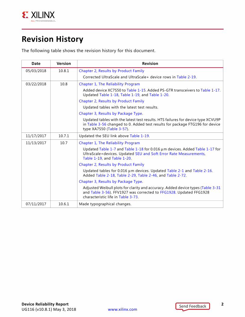
Revision HistoryThe following table shows the revision history for this document.
Date Version Revision
05/03/2018 10.8.1 Chapter 2, Results by Product Family
Corrected UltraScale and UltraScale+ device rows in Table 2-19.
03/22/2018 10.8 Chapter 1, The Reliability Program
Added device XC7S50 to Table 1-15. Added PS-GTR transceivers to Table 1-17. Updated Table 1-18, Table 1-19, and Table 1-20.
Chapter 2, Results by Product Family
Updated tables with the latest test results.
Chapter 3, Results by Package Type.
Updated tables with the latest test results. HTS failures for device type XCVU9P in Table 3-56 changed to 0. Added test results for package FTG196 for device type XA7S50 (Table 3-57).
11/17/2017 10.7.1 Updated the SEU link above Table 1-19.
11/13/2017 10.7 Chapter 1, The Reliability Program
Updated Table 1-7 and Table 1-18 for 0.016 μm devices. Added Table 1-17 for UltraScale+devices. Updated SEU and Soft Error Rate Measurements, Table 1-19, and Table 1-20.
Chapter 2, Results by Product Family
Updated tables for 0.016 μm devices. Updated Table 2-1 and Table 2-16. Added Table 2-18, Table 2-29, Table 2-46, and Table 2-72.
Chapter 3, Results by Package Type.
Adjusted Weibull plots for clarity and accuracy. Added device types (Table 3-31 and Table 3-56). FFV1927 was corrected to FFG1928. Updated FFG1928 characteristic life in Table 3-73.
07/11/2017 10.6.1 Made typographical changes.
Device Reliability Report 2UG116 (v10.8.1) May 3, 2018 www.xilinx.com
Send Feedback
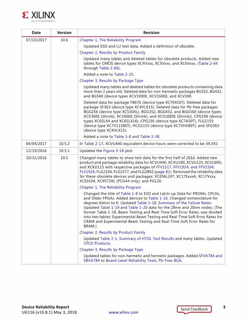
07/10/2017 10.6 Chapter 1, The Reliability Program
Updated ESD and LU test data. Added a definition of obsolete.
Chapter 2, Results by Product Family
Updated many tables and deleted tables for obsolete products. Added new tables for CMOS device types XC4Vxxx, XC5Vxxx, and XC6Vxxx, (Table 2-64 through Table 2-66).
Added a note to Table 2-25.
Chapter 3, Results by Package Type
Updated many tables and deleted tables for obsolete products containing data more than 2 years old. Deleted data for non-hermetic packages BG352, BG432, and BG560 (device types XCV1000E, XCV1600E, and XCV300.
Deleted data for package FB676 (device type XC7K410T). Deleted data for package SF363 (device type XC4VLX15). Deleted data for Pb-free packages BGG256 (device type XCS30XL), BGG352, BGG432, and BGG560 (device types XCV300E (Shrink), XCV600E (Shrink), and XCV1000E (Shrink)), CPG196 (device types XC6SLX4 and XC6SLX16), CPG236 (device type XC7A50T), FLG1155 (device type XC7V11580T), HCG1155 (device type XC7VH580T), and SFG363 (device type XC4VLX15).
Added a note to Table 3-8 and Table 3-38.
04/04/2017 10.5.2 In Table 2-17, XCVU440 equivalent device hours were corrected to be 34,592.
12/19/2016 10.5.1 Updated the Figure 3-18 plot.
10/31/2016 10.5 Changed many tables to show test data for the first half of 2016. Added new product and package reliability data for XCVU440, XCVU190, XCVU125, XCVU095, and XCKU115 with respective packages of FFV1517, FFV1924, and FFV2104, FLV1924, FLG2104, FLG2377, and FLG2892 (page 81). Removed the reliability data for these obsolete devices and packages: XCE06L24T, XC17SxxxA, XC17Vxxx, XCE0104, XC9572XL (PCG44 only), and PG120.
Chapter 1, The Reliability Program
Changed the title of Table 1-8 to ESD and Latch-up Data for PROMs, CPLDs, and Older FPGAs. Added devices to Table 1-16. Changed nomenclature for degrees Kelvin to K. Updated Table 1-18, Summary of the Failure Rates. Updated Table 1-19 and Table 1-20 data for the 28nm and 20nm nodes. (The former Table 1-18, Beam Testing and Real-Time Soft Error Rates, was divided into two tables: Experimental Beam Testing and Real-Time Soft Error Rates for CRAM and Experimental Beam Testing and Real-Time Soft Error Rates for BRAM.)
Chapter 2, Results by Product Family
Updated Table 2-1, Summary of HTOL Test Results and many tables. Updated CPLD Products.
Chapter 3, Results by Package Type
Updated tables for non-hermetic and hermetic packages. Added SFVA784 and SBVA784 to Board-Level Reliability Tests, Pb-Free BGA.
Date Version Revision
Device Reliability Report 3UG116 (v10.8.1) May 3, 2018 www.xilinx.com
Send Feedback
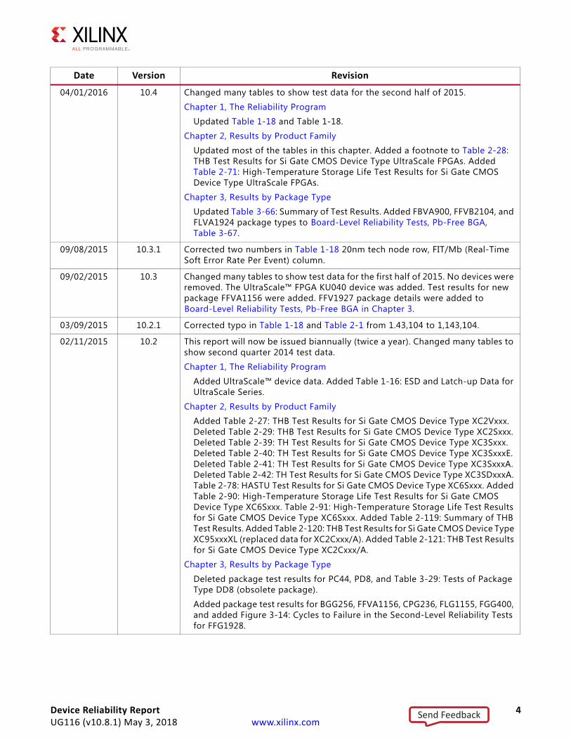
04/01/2016 10.4 Changed many tables to show test data for the second half of 2015.
Chapter 1, The Reliability Program
Updated Table 1-18 and Table 1-18.
Chapter 2, Results by Product Family
Updated most of the tables in this chapter. Added a footnote to Table 2-28: THB Test Results for Si Gate CMOS Device Type UltraScale FPGAs. Added Table 2-71: High-Temperature Storage Life Test Results for Si Gate CMOS Device Type UltraScale FPGAs.
Chapter 3, Results by Package Type
Updated Table 3-66: Summary of Test Results. Added FBVA900, FFVB2104, and FLVA1924 package types to Board-Level Reliability Tests, Pb-Free BGA, Table 3-67.
09/08/2015 10.3.1 Corrected two numbers in Table 1-18 20nm tech node row, FIT/Mb (Real-Time Soft Error Rate Per Event) column.
09/02/2015 10.3 Changed many tables to show test data for the first half of 2015. No devices were removed. The UltraScale™ FPGA KU040 device was added. Test results for new package FFVA1156 were added. FFV1927 package details were added to Board-Level Reliability Tests, Pb-Free BGA in Chapter 3.
03/09/2015 10.2.1 Corrected typo in Table 1-18 and Table 2-1 from 1.43,104 to 1,143,104.
02/11/2015 10.2 This report will now be issued biannually (twice a year). Changed many tables to show second quarter 2014 test data.
Chapter 1, The Reliability Program
Added UltraScale™ device data. Added Table 1-16: ESD and Latch-up Data for UltraScale Series.
Chapter 2, Results by Product Family
Added Table 2-27: THB Test Results for Si Gate CMOS Device Type XC2Vxxx. Deleted Table 2-29: THB Test Results for Si Gate CMOS Device Type XC2Sxxx. Deleted Table 2-39: TH Test Results for Si Gate CMOS Device Type XC3Sxxx. Deleted Table 2-40: TH Test Results for Si Gate CMOS Device Type XC3SxxxE. Deleted Table 2-41: TH Test Results for Si Gate CMOS Device Type XC3SxxxA. Deleted Table 2-42: TH Test Results for Si Gate CMOS Device Type XC3SDxxxA. Table 2-78: HASTU Test Results for Si Gate CMOS Device Type XC6Sxxx. Added Table 2-90: High-Temperature Storage Life Test Results for Si Gate CMOS Device Type XC6Sxxx. Table 2-91: High-Temperature Storage Life Test Results for Si Gate CMOS Device Type XC6Sxxx. Added Table 2-119: Summary of THB Test Results. Added Table 2-120: THB Test Results for Si Gate CMOS Device Type XC95xxxXL (replaced data for XC2Cxxx/A). Added Table 2-121: THB Test Results for Si Gate CMOS Device Type XC2Cxxx/A.
Chapter 3, Results by Package Type
Deleted package test results for PC44, PD8, and Table 3-29: Tests of Package Type DD8 (obsolete package).
Added package test results for BGG256, FFVA1156, CPG236, FLG1155, FGG400, and added Figure 3-14: Cycles to Failure in the Second-Level Reliability Tests for FFG1928.
Date Version Revision
Device Reliability Report 4UG116 (v10.8.1) May 3, 2018 www.xilinx.com
Send Feedback
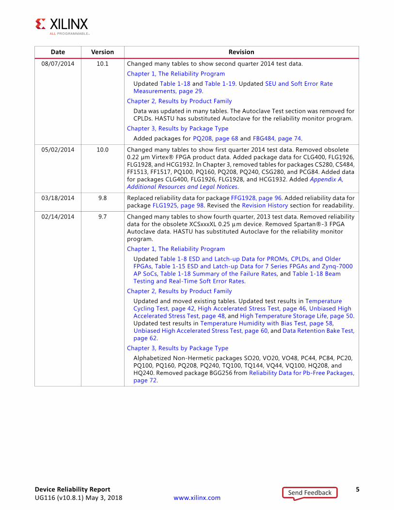
08/07/2014 10.1 Changed many tables to show second quarter 2014 test data.
Chapter 1, The Reliability Program
Updated Table 1-18 and Table 1-19. Updated SEU and Soft Error Rate Measurements, page 29.
Chapter 2, Results by Product Family
Data was updated in many tables. The Autoclave Test section was removed for CPLDs. HASTU has substituted Autoclave for the reliability monitor program.
Chapter 3, Results by Package Type
Added packages for PQ208, page 68 and FBG484, page 74.
05/02/2014 10.0 Changed many tables to show first quarter 2014 test data. Removed obsolete 0.22 µm Virtex® FPGA product data. Added package data for CLG400, FLG1926, FLG1928, and HCG1932. In Chapter 3, removed tables for packages CS280, CS484, FF1513, FF1517, PQ100, PQ160, PQ208, PQ240, CSG280, and PCG84. Added data for packages CLG400, FLG1926, FLG1928, and HCG1932. Added Appendix A, Additional Resources and Legal Notices.
03/18/2014 9.8 Replaced reliability data for package FFG1928, page 96. Added reliability data for package FLG1925, page 98. Revised the Revision History section for readability.
02/14/2014 9.7 Changed many tables to show fourth quarter, 2013 test data. Removed reliability data for the obsolete XCSxxxXL 0.25 μm device. Removed Spartan®-3 FPGA Autoclave data. HASTU has substituted Autoclave for the reliability monitor program.
Chapter 1, The Reliability Program
Updated Table 1-8 ESD and Latch-up Data for PROMs, CPLDs, and Older FPGAs, Table 1-15 ESD and Latch-up Data for 7 Series FPGAs and Zynq-7000 AP SoCs, Table 1-18 Summary of the Failure Rates, and Table 1-18 Beam Testing and Real-Time Soft Error Rates.
Chapter 2, Results by Product Family
Updated and moved existing tables. Updated test results in Temperature Cycling Test, page 42, High Accelerated Stress Test, page 46, Unbiased High Accelerated Stress Test, page 48, and High Temperature Storage Life, page 50. Updated test results in Temperature Humidity with Bias Test, page 58, Unbiased High Accelerated Stress Test, page 60, and Data Retention Bake Test, page 62.
Chapter 3, Results by Package Type
Alphabetized Non-Hermetic packages SO20, VO20, VO48, PC44, PC84, PC20, PQ100, PQ160, PQ208, PQ240, TQ100, TQ144, VQ44, VQ100, HQ208, and HQ240. Removed package BGG256 from Reliability Data for Pb-Free Packages, page 72.
Date Version Revision
Device Reliability Report 5UG116 (v10.8.1) May 3, 2018 www.xilinx.com
Send Feedback
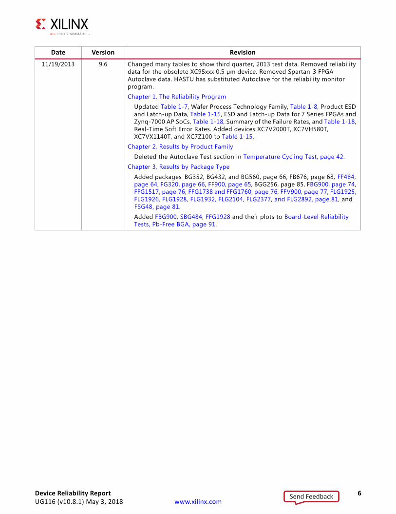
11/19/2013 9.6 Changed many tables to show third quarter, 2013 test data. Removed reliability data for the obsolete XC95xxx 0.5 µm device. Removed Spartan-3 FPGA Autoclave data. HASTU has substituted Autoclave for the reliability monitor program.
Chapter 1, The Reliability Program
Updated Table 1-7, Wafer Process Technology Family, Table 1-8, Product ESD and Latch-up Data, Table 1-15, ESD and Latch-up Data for 7 Series FPGAs and Zynq-7000 AP SoCs, Table 1-18, Summary of the Failure Rates, and Table 1-18, Real-Time Soft Error Rates. Added devices XC7V2000T, XC7VH580T, XC7VX1140T, and XC7Z100 to Table 1-15.
Chapter 2, Results by Product Family
Deleted the Autoclave Test section in Temperature Cycling Test, page 42.
Chapter 3, Results by Package Type
Added packages BG352, BG432, and BG560, page 66, FB676, page 68, FF484, page 64, FG320, page 66, FF900, page 65, BGG256, page 85, FBG900, page 74, FFG1517, page 76, FFG1738 and FFG1760, page 76, FFV900, page 77, FLG1925, FLG1926, FLG1928, FLG1932, FLG2104, FLG2377, and FLG2892, page 81, and FSG48, page 81.
Added FBG900, SBG484, FFG1928 and their plots to Board-Level Reliability Tests, Pb-Free BGA, page 91.
Date Version Revision
Device Reliability Report 6UG116 (v10.8.1) May 3, 2018 www.xilinx.com
Send Feedback
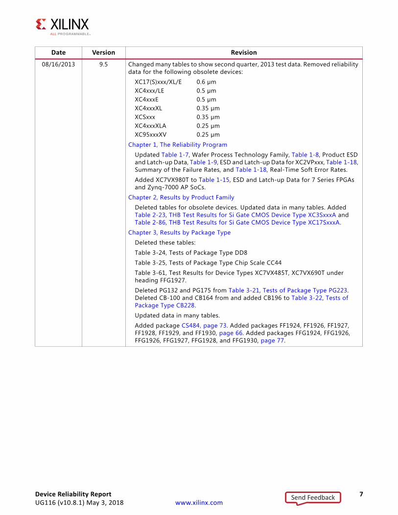
08/16/2013 9.5 Changed many tables to show second quarter, 2013 test data. Removed reliability data for the following obsolete devices:
XC17(S)xxx/XL/E 0.6 µmXC4xxx/LE 0.5 µmXC4xxxE 0.5 µmXC4xxxXL 0.35 µmXCSxxx 0.35 µmXC4xxxXLA 0.25 µmXC95xxxXV 0.25 µm
Chapter 1, The Reliability Program
Updated Table 1-7, Wafer Process Technology Family, Table 1-8, Product ESD and Latch-up Data, Table 1-9, ESD and Latch-up Data for XC2VPxxx, Table 1-18, Summary of the Failure Rates, and Table 1-18, Real-Time Soft Error Rates.
Added XC7VX980T to Table 1-15, ESD and Latch-up Data for 7 Series FPGAs and Zynq-7000 AP SoCs.
Chapter 2, Results by Product Family
Deleted tables for obsolete devices. Updated data in many tables. Added Table 2-23, THB Test Results for Si Gate CMOS Device Type XC3SxxxA and Table 2-86, THB Test Results for Si Gate CMOS Device Type XC17SxxxA.
Chapter 3, Results by Package Type
Deleted these tables:
Table 3-24, Tests of Package Type DD8
Table 3-25, Tests of Package Type Chip Scale CC44
Table 3-61, Test Results for Device Types XC7VX485T, XC7VX690T under heading FFG1927.
Deleted PG132 and PG175 from Table 3-21, Tests of Package Type PG223. Deleted CB-100 and CB164 from and added CB196 to Table 3-22, Tests of Package Type CB228.
Updated data in many tables.
Added package CS484, page 73. Added packages FF1924, FF1926, FF1927, FF1928, FF1929, and FF1930, page 66. Added packages FFG1924, FFG1926, FFG1926, FFG1927, FFG1928, and FFG1930, page 77.
Date Version Revision
Device Reliability Report 7UG116 (v10.8.1) May 3, 2018 www.xilinx.com
Send Feedback
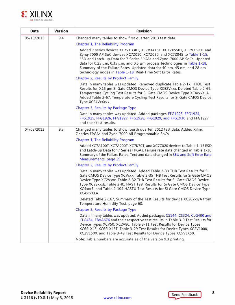
05/13/2013 9.4 Changed many tables to show first quarter, 2013 test data.
Chapter 1, The Reliability Program
Added 7 series devices XC7VX330T, XC7VX415T, XC7VX550T, XC7VX690T and Zynq-7000 AP SoC devices XC7Z010, XC7Z030, and XC7Z045 to Table 1-15, ESD and Latch-up Data for 7 Series FPGAs and Zynq-7000 AP SoCs. Updated data for 0.25 μm, 0.35 μm, and 0.5 μm process technologies in Table 1-18, Summary of the Failure Rates. Updated data for 40 nm, 45 nm, and 28 nm technology nodes in Table 1-18, Real-Time Soft Error Rates.
Chapter 2, Results by Product Family
Data in many tables was updated. Removed duplicate Table 2-17, HTOL Test Results for 0.15 µm Si Gate CMOS Device Type XCE2Vxxx. Deleted Table 2-69, Temperature Cycling Test Results for Si Gate CMOS Device Type XC4xxxXLA. Added Table 2-67, Temperature Cycling Test Results for Si Gate CMOS Device Type XCE4VxXxxx.
Chapter 3, Results by Package Type
Data in many tables was updated. Added packages FFG1923, FFG1924, FFG1925, FFG1926, FFG1927, FFG1928, FFG1929, and FFG1930 and FFG1927 and their test results.
04/02/2013 9.3 Changed many tables to show fourth quarter, 2012 test data. Added Xilinx 7 series FPGAs and Zynq-7000 All Programmable SoCs.
Chapter 1, The Reliability Program
Added XC7A100T, XC7A200T, XC7K70T, and XC7Z020 devices to Table 1-15 ESD and Latch-up Data for 7 Series FPGAs. Failure rate data changed in Table 1-16 Summary of the Failure Rates. Text and data changed in SEU and Soft Error Rate Measurements, page 29.
Chapter 2, Results by Product Family
Data in many tables was updated. Added Table 2-33 THB Test Results for Si Gate CMOS Device Type XCVxxx, Table 2-35 THB Test Results for Si Gate CMOS Device Type XC2Vxxx, Table 2-32 THB Test Results for Si Gate CMOS Device Type XC2SxxxE, Table 2-81 HAST Test Results for Si Gate CMOS Device Type XC4xxxE, and Table 2-104 HASTU Test Results for Si Gate CMOS Device Type XC4xxxXLA.
Deleted Table 2-167, Summary of the Test Results for device XC2Cxxx/A from Temperature Humidity Test, page 68.
Chapter 3, Results by Package Type
Data in many tables was updated. Added packages CS144, CS324, CLG400 and CLG484, FBVA676 and their respective test results in Table 3-9 Test Results for Device Types XCV50, XC2V80, Table 3-11 Test Results for Device Types XC6SLX45, XC6SLX45T, Table 3-29 Test Results for Device Types XC2V1000, XC2V1500, and Table 3-49 Test Results for Device Types XC5VLX50.
Note: Table numbers are accurate as of the version 9.3 printing.
Date Version Revision
Device Reliability Report 8UG116 (v10.8.1) May 3, 2018 www.xilinx.com
Send Feedback
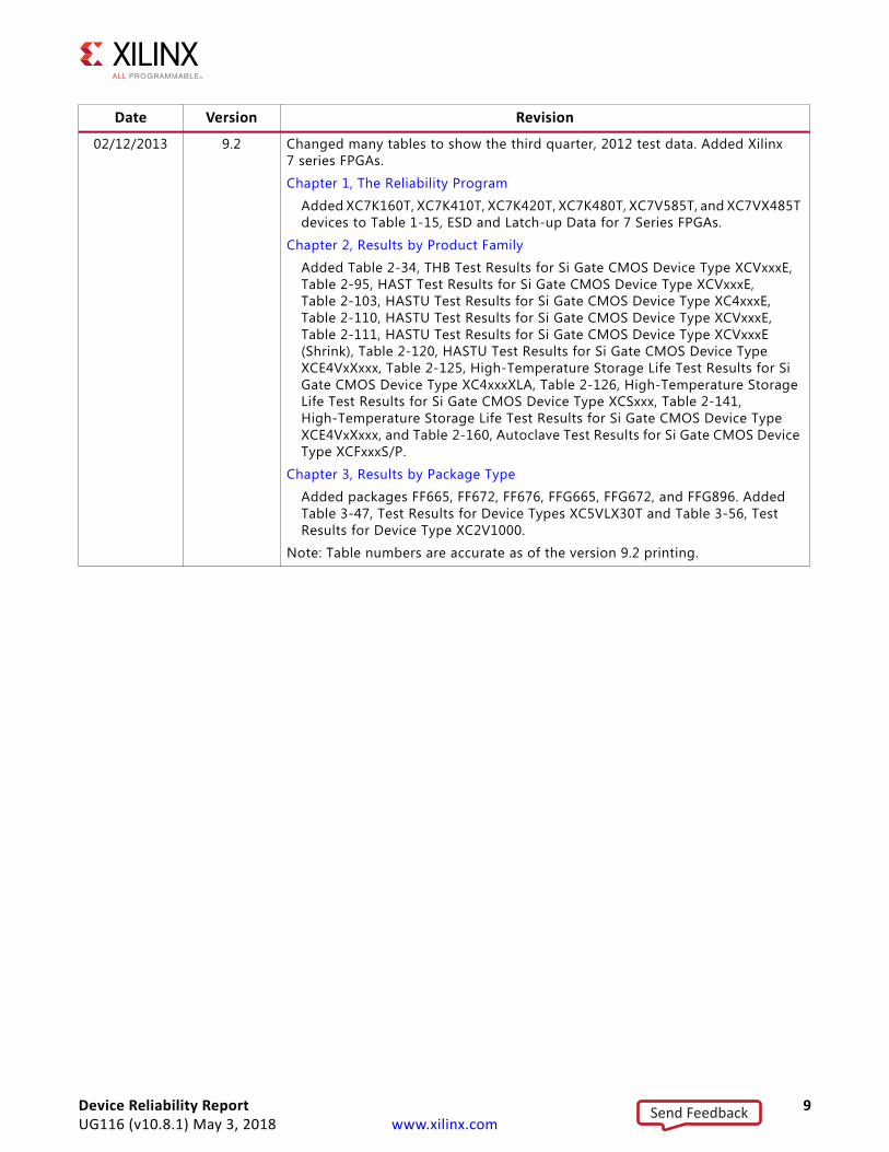
02/12/2013 9.2 Changed many tables to show the third quarter, 2012 test data. Added Xilinx 7 series FPGAs.
Chapter 1, The Reliability Program
Added XC7K160T, XC7K410T, XC7K420T, XC7K480T, XC7V585T, and XC7VX485T devices to Table 1-15, ESD and Latch-up Data for 7 Series FPGAs.
Chapter 2, Results by Product Family
Added Table 2-34, THB Test Results for Si Gate CMOS Device Type XCVxxxE, Table 2-95, HAST Test Results for Si Gate CMOS Device Type XCVxxxE, Table 2-103, HASTU Test Results for Si Gate CMOS Device Type XC4xxxE, Table 2-110, HASTU Test Results for Si Gate CMOS Device Type XCVxxxE, Table 2-111, HASTU Test Results for Si Gate CMOS Device Type XCVxxxE (Shrink), Table 2-120, HASTU Test Results for Si Gate CMOS Device Type XCE4VxXxxx, Table 2-125, High-Temperature Storage Life Test Results for Si Gate CMOS Device Type XC4xxxXLA, Table 2-126, High-Temperature Storage Life Test Results for Si Gate CMOS Device Type XCSxxx, Table 2-141, High-Temperature Storage Life Test Results for Si Gate CMOS Device Type XCE4VxXxxx, and Table 2-160, Autoclave Test Results for Si Gate CMOS Device Type XCFxxxS/P.
Chapter 3, Results by Package Type
Added packages FF665, FF672, FF676, FFG665, FFG672, and FFG896. Added Table 3-47, Test Results for Device Types XC5VLX30T and Table 3-56, Test Results for Device Type XC2V1000.
Note: Table numbers are accurate as of the version 9.2 printing.
Date Version Revision
Device Reliability Report 9UG116 (v10.8.1) May 3, 2018 www.xilinx.com
Send Feedback
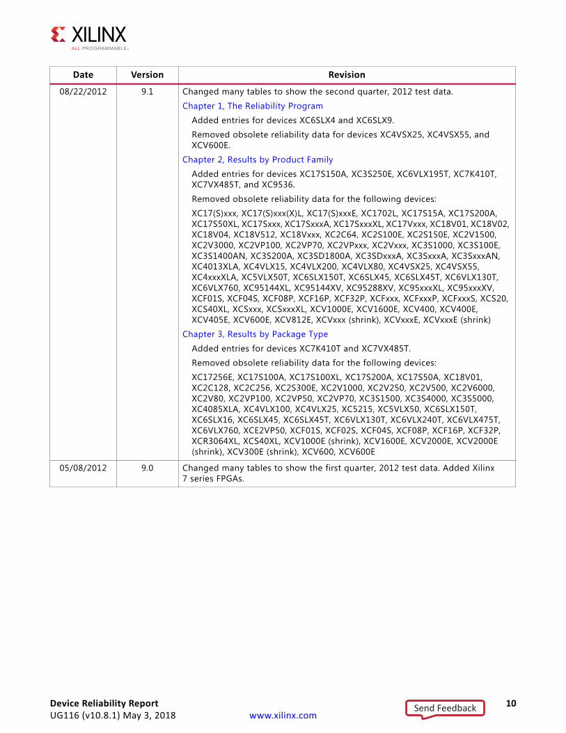
08/22/2012 9.1 Changed many tables to show the second quarter, 2012 test data.
Chapter 1, The Reliability Program
Added entries for devices XC6SLX4 and XC6SLX9.
Removed obsolete reliability data for devices XC4VSX25, XC4VSX55, and XCV600E.
Chapter 2, Results by Product Family
Added entries for devices XC17S150A, XC3S250E, XC6VLX195T, XC7K410T, XC7VX485T, and XC9536.
Removed obsolete reliability data for the following devices:
XC17(S)xxx, XC17(S)xxx(X)L, XC17(S)xxxE, XC1702L, XC17S15A, XC17S200A, XC17S50XL, XC17Sxxx, XC17SxxxA, XC17SxxxXL, XC17Vxxx, XC18V01, XC18V02, XC18V04, XC18V512, XC18Vxxx, XC2C64, XC2S100E, XC2S150E, XC2V1500, XC2V3000, XC2VP100, XC2VP70, XC2VPxxx, XC2Vxxx, XC3S1000, XC3S100E, XC3S1400AN, XC3S200A, XC3SD1800A, XC3SDxxxA, XC3SxxxA, XC3SxxxAN, XC4013XLA, XC4VLX15, XC4VLX200, XC4VLX80, XC4VSX25, XC4VSX55, XC4xxxXLA, XC5VLX50T, XC6SLX150T, XC6SLX45, XC6SLX45T, XC6VLX130T, XC6VLX760, XC95144XL, XC95144XV, XC95288XV, XC95xxxXL, XC95xxxXV, XCF01S, XCF04S, XCF08P, XCF16P, XCF32P, XCFxxx, XCFxxxP, XCFxxxS, XCS20, XCS40XL, XCSxxx, XCSxxxXL, XCV1000E, XCV1600E, XCV400, XCV400E, XCV405E, XCV600E, XCV812E, XCVxxx (shrink), XCVxxxE, XCVxxxE (shrink)
Chapter 3, Results by Package Type
Added entries for devices XC7K410T and XC7VX485T.
Removed obsolete reliability data for the following devices:
XC17256E, XC17S100A, XC17S100XL, XC17S200A, XC17S50A, XC18V01, XC2C128, XC2C256, XC2S300E, XC2V1000, XC2V250, XC2V500, XC2V6000, XC2V80, XC2VP100, XC2VP50, XC2VP70, XC3S1500, XC3S4000, XC3S5000, XC4085XLA, XC4VLX100, XC4VLX25, XC5215, XC5VLX50, XC6SLX150T, XC6SLX16, XC6SLX45, XC6SLX45T, XC6VLX130T, XC6VLX240T, XC6VLX475T, XC6VLX760, XCE2VP50, XCF01S, XCF02S, XCF04S, XCF08P, XCF16P, XCF32P, XCR3064XL, XCS40XL, XCV1000E (shrink), XCV1600E, XCV2000E, XCV2000E (shrink), XCV300E (shrink), XCV600, XCV600E
05/08/2012 9.0 Changed many tables to show the first quarter, 2012 test data. Added Xilinx 7 series FPGAs.
Date Version Revision
Device Reliability Report 10UG116 (v10.8.1) May 3, 2018 www.xilinx.com
Send Feedback
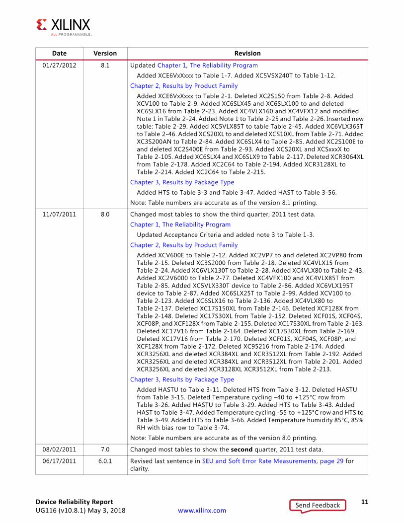
01/27/2012 8.1 Updated Chapter 1, The Reliability Program
Added XCE6VxXxxx to Table 1-7. Added XC5VSX240T to Table 1-12.
Chapter 2, Results by Product Family
Added XCE6VxXxxx to Table 2-1. Deleted XC2S150 from Table 2-8. Added XCV100 to Table 2-9. Added XC6SLX45 and XC6SLX100 to and deleted XC6SLX16 from Table 2-23. Added XC4VLX160 and XC4VFX12 and modified Note 1 in Table 2-24. Added Note 1 to Table 2-25 and Table 2-26. Inserted new table: Table 2-29. Added XC5VLX85T to table Table 2-45. Added XC6VLX365T to Table 2-46. Added XCS20XL to and deleted XCS10XL from Table 2-71. Added XC3S200AN to Table 2-84. Added XC6SLX4 to Table 2-85. Added XC2S100E to and deleted XC2S400E from Table 2-93. Added XCS20XL and XCSxxxX to Table 2-105. Added XC6SLX4 and XC6SLX9 to Table 2-117. Deleted XCR3064XL from Table 2-178. Added XC2C64 to Table 2-194. Added XCR3128XL to Table 2-214. Added XC2C64 to Table 2-215.
Chapter 3, Results by Package Type
Added HTS to Table 3-3 and Table 3-47. Added HAST to Table 3-56.
Note: Table numbers are accurate as of the version 8.1 printing.
11/07/2011 8.0 Changed most tables to show the third quarter, 2011 test data.
Chapter 1, The Reliability Program
Updated Acceptance Criteria and added note 3 to Table 1-3.
Chapter 2, Results by Product Family
Added XCV600E to Table 2-12. Added XC2VP7 to and deleted XC2VP80 from Table 2-15. Deleted XC3S2000 from Table 2-18. Deleted XC4VLX15 from Table 2-24. Added XC6VLX130T to Table 2-28. Added XC4VLX80 to Table 2-43. Added XC2V6000 to Table 2-77. Deleted XC4VFX100 and XC4VLX85T from Table 2-85. Added XC5VLX330T device to Table 2-86. Added XC6VLX195T device to Table 2-87. Added XC6SLX25T to Table 2-99. Added XCV100 to Table 2-123. Added XC6SLX16 to Table 2-136. Added XC4VLX80 to Table 2-137. Deleted XC17S150XL from Table 2-146. Deleted XCF128X from Table 2-148. Deleted XC17S30XL from Table 2-152. Deleted XCF01S, XCF04S, XCF08P, and XCF128X from Table 2-155. Deleted XC17S30XL from Table 2-163. Deleted XC17V16 from Table 2-164. Deleted XC17S30XL from Table 2-169. Deleted XC17V16 from Table 2-170. Deleted XCF01S, XCF04S, XCF08P, and XCF128X from Table 2-172. Deleted XC95216 from Table 2-174. Added XCR3256XL and deleted XCR384XL and XCR3512XL from Table 2-192. Added XCR3256XL and deleted XCR384XL and XCR3512XL from Table 2-201. Added XCR3256XL and deleted XCR3128XL XCR3512XL from Table 2-213.
Chapter 3, Results by Package Type
Added HASTU to Table 3-11. Deleted HTS from Table 3-12. Deleted HASTU from Table 3-15. Deleted Temperature cycling –40 to +125°C row from Table 3-26. Added HASTU to Table 3-29. Added HTS to Table 3-43. Added HAST to Table 3-47. Added Temperature cycling -55 to +125°C row and HTS to Table 3-49. Added HTS to Table 3-66. Added Temperature humidity 85°C, 85% RH with bias row to Table 3-74.
Note: Table numbers are accurate as of the version 8.0 printing.
08/02/2011 7.0 Changed most tables to show the second quarter, 2011 test data.
06/17/2011 6.0.1 Revised last sentence in SEU and Soft Error Rate Measurements, page 29 for clarity.
Date Version Revision
Device Reliability Report 11UG116 (v10.8.1) May 3, 2018 www.xilinx.com
Send Feedback
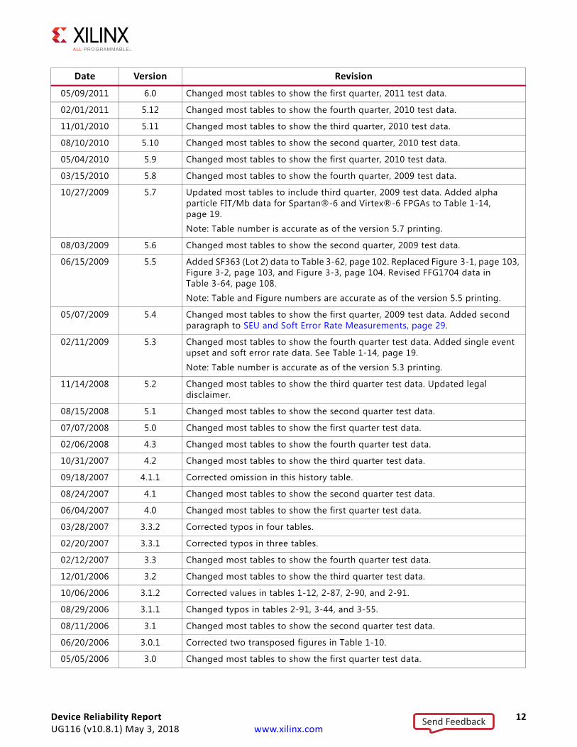
05/09/2011 6.0 Changed most tables to show the first quarter, 2011 test data.
02/01/2011 5.12 Changed most tables to show the fourth quarter, 2010 test data.
11/01/2010 5.11 Changed most tables to show the third quarter, 2010 test data.
08/10/2010 5.10 Changed most tables to show the second quarter, 2010 test data.
05/04/2010 5.9 Changed most tables to show the first quarter, 2010 test data.
03/15/2010 5.8 Changed most tables to show the fourth quarter, 2009 test data.
10/27/2009 5.7 Updated most tables to include third quarter, 2009 test data. Added alpha particle FIT/Mb data for Spartan®-6 and Virtex®-6 FPGAs to Table 1-14, page 19.
Note: Table number is accurate as of the version 5.7 printing.
08/03/2009 5.6 Changed most tables to show the second quarter, 2009 test data.
06/15/2009 5.5 Added SF363 (Lot 2) data to Table 3-62, page 102. Replaced Figure 3-1, page 103, Figure 3-2, page 103, and Figure 3-3, page 104. Revised FFG1704 data in Table 3-64, page 108.
Note: Table and Figure numbers are accurate as of the version 5.5 printing.
05/07/2009 5.4 Changed most tables to show the first quarter, 2009 test data. Added second paragraph to SEU and Soft Error Rate Measurements, page 29.
02/11/2009 5.3 Changed most tables to show the fourth quarter test data. Added single event upset and soft error rate data. See Table 1-14, page 19.
Note: Table number is accurate as of the version 5.3 printing.
11/14/2008 5.2 Changed most tables to show the third quarter test data. Updated legal disclaimer.
08/15/2008 5.1 Changed most tables to show the second quarter test data.
07/07/2008 5.0 Changed most tables to show the first quarter test data.
02/06/2008 4.3 Changed most tables to show the fourth quarter test data.
10/31/2007 4.2 Changed most tables to show the third quarter test data.
09/18/2007 4.1.1 Corrected omission in this history table.
08/24/2007 4.1 Changed most tables to show the second quarter test data.
06/04/2007 4.0 Changed most tables to show the first quarter test data.
03/28/2007 3.3.2 Corrected typos in four tables.
02/20/2007 3.3.1 Corrected typos in three tables.
02/12/2007 3.3 Changed most tables to show the fourth quarter test data.
12/01/2006 3.2 Changed most tables to show the third quarter test data.
10/06/2006 3.1.2 Corrected values in tables 1-12, 2-87, 2-90, and 2-91.
08/29/2006 3.1.1 Changed typos in tables 2-91, 3-44, and 3-55.
08/11/2006 3.1 Changed most tables to show the second quarter test data.
06/20/2006 3.0.1 Corrected two transposed figures in Table 1-10.
05/05/2006 3.0 Changed most tables to show the first quarter test data.
Date Version Revision
Device Reliability Report 12UG116 (v10.8.1) May 3, 2018 www.xilinx.com
Send Feedback
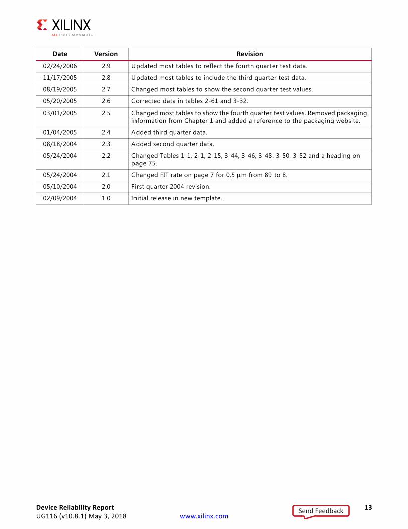
02/24/2006 2.9 Updated most tables to reflect the fourth quarter test data.
11/17/2005 2.8 Updated most tables to include the third quarter test data.
08/19/2005 2.7 Changed most tables to show the second quarter test values.
05/20/2005 2.6 Corrected data in tables 2-61 and 3-32.
03/01/2005 2.5 Changed most tables to show the fourth quarter test values. Removed packaging information from Chapter 1 and added a reference to the packaging website.
01/04/2005 2.4 Added third quarter data.
08/18/2004 2.3 Added second quarter data.
05/24/2004 2.2 Changed Tables 1-1, 2-1, 2-15, 3-44, 3-46, 3-48, 3-50, 3-52 and a heading on page 75.
05/24/2004 2.1 Changed FIT rate on page 7 for 0.5 μm from 89 to 8.
05/10/2004 2.0 First quarter 2004 revision.
02/09/2004 1.0 Initial release in new template.
Date Version Revision
Device Reliability Report 13UG116 (v10.8.1) May 3, 2018 www.xilinx.com
Send Feedback
Device Reliability Report 14UG116 (v10.8.1) May 3, 2018 www.xilinx.com
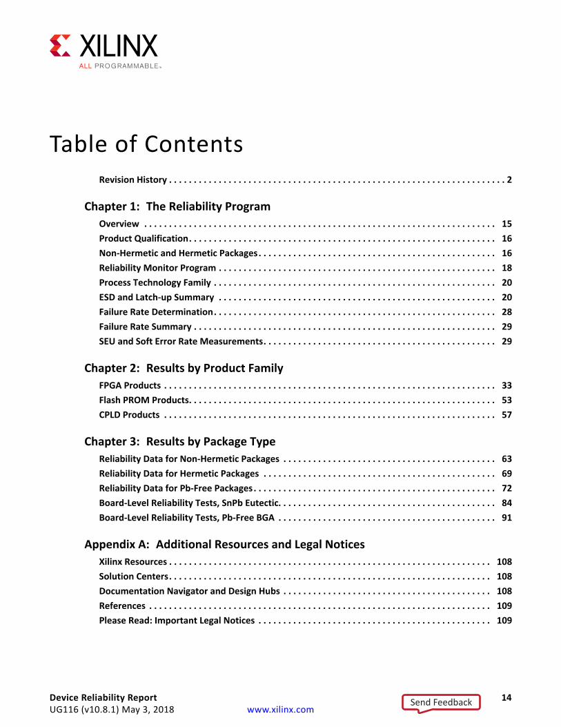
Table of ContentsRevision History . . . . . . . . . . . . . . . . . . . . . . . . . . . . . . . . . . . . . . . . . . . . . . . . . . . . . . . . . . . . . . . . . . . . 2
Chapter 1: The Reliability ProgramOverview . . . . . . . . . . . . . . . . . . . . . . . . . . . . . . . . . . . . . . . . . . . . . . . . . . . . . . . . . . . . . . . . . . . . . . . 15Product Qualification. . . . . . . . . . . . . . . . . . . . . . . . . . . . . . . . . . . . . . . . . . . . . . . . . . . . . . . . . . . . . . 16Non-Hermetic and Hermetic Packages. . . . . . . . . . . . . . . . . . . . . . . . . . . . . . . . . . . . . . . . . . . . . . . . 16Reliability Monitor Program . . . . . . . . . . . . . . . . . . . . . . . . . . . . . . . . . . . . . . . . . . . . . . . . . . . . . . . . 18Process Technology Family . . . . . . . . . . . . . . . . . . . . . . . . . . . . . . . . . . . . . . . . . . . . . . . . . . . . . . . . . 20ESD and Latch-up Summary . . . . . . . . . . . . . . . . . . . . . . . . . . . . . . . . . . . . . . . . . . . . . . . . . . . . . . . . 20Failure Rate Determination. . . . . . . . . . . . . . . . . . . . . . . . . . . . . . . . . . . . . . . . . . . . . . . . . . . . . . . . . 28Failure Rate Summary . . . . . . . . . . . . . . . . . . . . . . . . . . . . . . . . . . . . . . . . . . . . . . . . . . . . . . . . . . . . . 29SEU and Soft Error Rate Measurements. . . . . . . . . . . . . . . . . . . . . . . . . . . . . . . . . . . . . . . . . . . . . . . 29
Chapter 2: Results by Product FamilyFPGA Products . . . . . . . . . . . . . . . . . . . . . . . . . . . . . . . . . . . . . . . . . . . . . . . . . . . . . . . . . . . . . . . . . . . 33Flash PROM Products. . . . . . . . . . . . . . . . . . . . . . . . . . . . . . . . . . . . . . . . . . . . . . . . . . . . . . . . . . . . . . 53CPLD Products . . . . . . . . . . . . . . . . . . . . . . . . . . . . . . . . . . . . . . . . . . . . . . . . . . . . . . . . . . . . . . . . . . . 57
Chapter 3: Results by Package TypeReliability Data for Non-Hermetic Packages . . . . . . . . . . . . . . . . . . . . . . . . . . . . . . . . . . . . . . . . . . . 63Reliability Data for Hermetic Packages . . . . . . . . . . . . . . . . . . . . . . . . . . . . . . . . . . . . . . . . . . . . . . . 69Reliability Data for Pb-Free Packages. . . . . . . . . . . . . . . . . . . . . . . . . . . . . . . . . . . . . . . . . . . . . . . . . 72Board-Level Reliability Tests, SnPb Eutectic. . . . . . . . . . . . . . . . . . . . . . . . . . . . . . . . . . . . . . . . . . . . 84Board-Level Reliability Tests, Pb-Free BGA . . . . . . . . . . . . . . . . . . . . . . . . . . . . . . . . . . . . . . . . . . . . 91
Appendix A: Additional Resources and Legal NoticesXilinx Resources . . . . . . . . . . . . . . . . . . . . . . . . . . . . . . . . . . . . . . . . . . . . . . . . . . . . . . . . . . . . . . . . . 108Solution Centers. . . . . . . . . . . . . . . . . . . . . . . . . . . . . . . . . . . . . . . . . . . . . . . . . . . . . . . . . . . . . . . . . 108Documentation Navigator and Design Hubs . . . . . . . . . . . . . . . . . . . . . . . . . . . . . . . . . . . . . . . . . . 108References . . . . . . . . . . . . . . . . . . . . . . . . . . . . . . . . . . . . . . . . . . . . . . . . . . . . . . . . . . . . . . . . . . . . . 109Please Read: Important Legal Notices . . . . . . . . . . . . . . . . . . . . . . . . . . . . . . . . . . . . . . . . . . . . . . . 109
Send Feedback
Chapter 1
The Reliability Program
OverviewXilinx publishes this report to provide customers with insight regarding the reliability of Xilinx® products. Reliability is defined as product performance to specification over time in response to varied (specified) environmental stress conditions. The goal of the reliability program is to achieve continuous improvement in the robustness of each product being evaluated.
As part of this program, finished product reliability is measured periodically to ensure that the product performance meets or exceeds reliability specifications. Reliability programs are executed in response to internal programs.
The reliability qualifications of new devices, wafer processes, and packages are designed to ensure that Xilinx products satisfy internal requirements before transfer into production. The reliability qualification and monitoring requirements are outlined in Table 1-1 through Table 1-18. The reliability stress tests are conducted according to the conditions specified in JEDEC Solid State Technology Association' s reliability test methods for packaged devices, JESD22, except Group B and D tests in which it follows DSCC test methods, MIL-STD-883.
Note: In this report, obsolete refers to Xilinx products for which a Product Discontinuation Notice (PDN) has been issued to cease the shipment and to data more than two years old that is no longer valid due to a process change.
Device Reliability Report 15UG116 (v10.8.1) May 3, 2018 www.xilinx.com
Send Feedback
Chapter 1: The Reliability Program
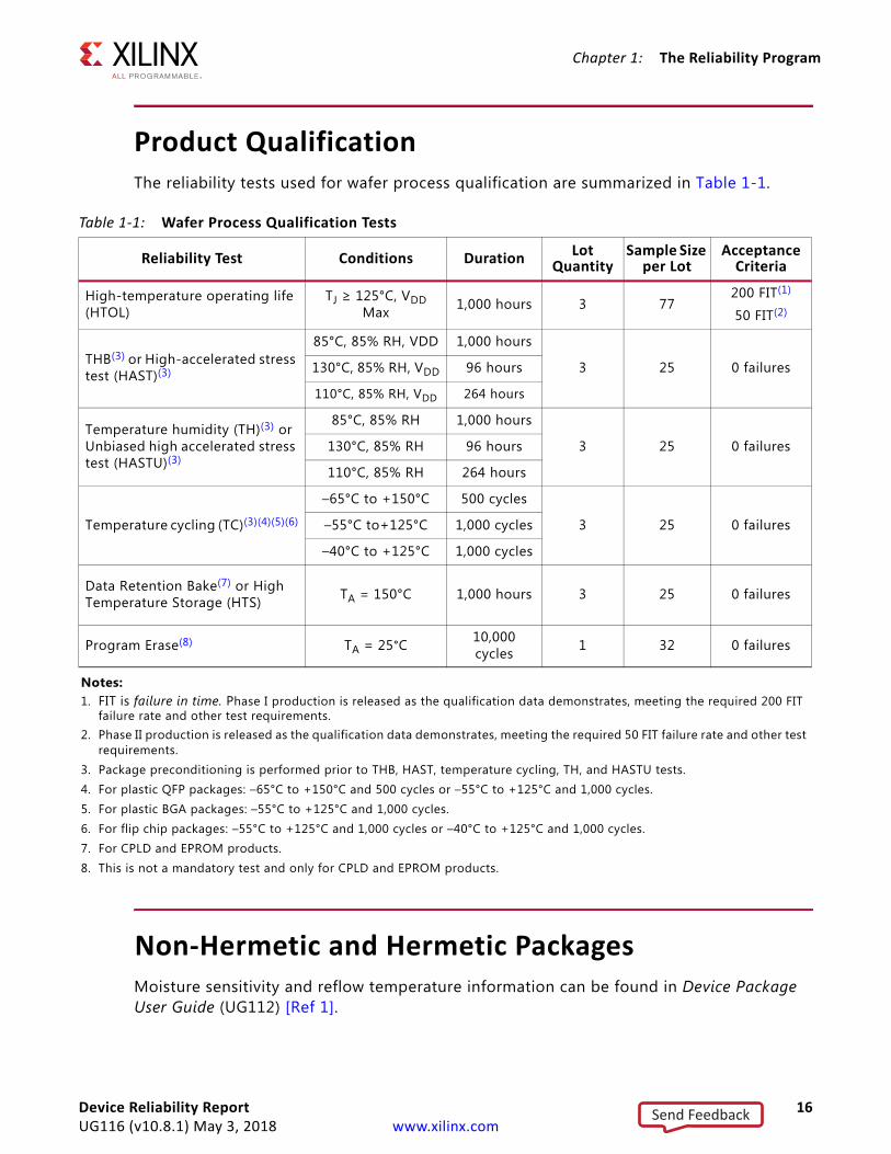
Product QualificationThe reliability tests used for wafer process qualification are summarized in Table 1-1.
Non-Hermetic and Hermetic PackagesMoisture sensitivity and reflow temperature information can be found in Device Package User Guide (UG112) [Ref 1].
Table 1-1: Wafer Process Qualification Tests
Reliability Test Conditions Duration Lot Quantity
Sample Size per Lot
Acceptance Criteria
High-temperature operating life (HTOL)
TJ ≥ 125°C, VDD Max 1,000 hours 3 77
200 FIT(1)
50 FIT(2)
THB(3) or High-accelerated stress test (HAST)(3)
85°C, 85% RH, VDD 1,000 hours
3 25 0 failures130°C, 85% RH, VDD 96 hours
110°C, 85% RH, VDD 264 hours
Temperature humidity (TH)(3) or Unbiased high accelerated stress test (HASTU)(3)
85°C, 85% RH 1,000 hours
3 25 0 failures130°C, 85% RH 96 hours
110°C, 85% RH 264 hours
Temperature cycling (TC)(3)(4)(5)(6)
–65°C to +150°C 500 cycles
3 25 0 failures–55°C to+125°C 1,000 cycles
–40°C to +125°C 1,000 cycles
Data Retention Bake(7) or High Temperature Storage (HTS) TA = 150°C 1,000 hours 3 25 0 failures
Program Erase(8) TA = 25°C 10,000 cycles 1 32 0 failures
Notes: 1. FIT is failure in time. Phase I production is released as the qualification data demonstrates, meeting the required 200 FIT
failure rate and other test requirements.2. Phase II production is released as the qualification data demonstrates, meeting the required 50 FIT failure rate and other test
requirements.3. Package preconditioning is performed prior to THB, HAST, temperature cycling, TH, and HASTU tests.4. For plastic QFP packages: –65°C to +150°C and 500 cycles or –55°C to +125°C and 1,000 cycles.5. For plastic BGA packages: –55°C to +125°C and 1,000 cycles.6. For flip chip packages: –55°C to +125°C and 1,000 cycles or –40°C to +125°C and 1,000 cycles.7. For CPLD and EPROM products.8. This is not a mandatory test and only for CPLD and EPROM products.
Device Reliability Report 16UG116 (v10.8.1) May 3, 2018 www.xilinx.com
Send Feedback
Chapter 1: The Reliability Program
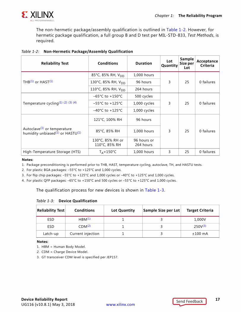
The non-hermetic package/assembly qualification is outlined in Table 1-2. However, for hermetic package qualification, a full group B and D test per MIL-STD-833, Test Methods, is required.
The qualification process for new devices is shown in Table 1-3.
Table 1-2: Non-Hermetic Package/Assembly Qualification
Reliability Test Conditions Duration Lot Quantity
Sample Size per
LotAcceptance
Criteria
THB(1) or HAST(1)
85°C, 85% RH, VDD 1,000 hours
3 25 0 failures130°C, 85% RH, VDD 96 hours
110°C, 85% RH, VDD 264 hours
Temperature cycling(1) (2) (3) (4)
–65°C to +150°C 500 cycles
3 25 0 failures–55°C to +125°C 1,000 cycles
–40°C to +125°C 1,000 cycles
Autoclave(1) or temperature humidity unbiased(1) or HASTU(1)
121°C, 100% RH 96 hours
3 25 0 failures85°C, 85% RH 1,000 hours
130°C, 85% RH or110°C, 85% RH
96 hours or 264 hours
High-Temperature Storage (HTS) TA=150°C 1,000 hours 3 25 0 failures
Notes: 1. Package preconditioning is performed prior to THB, HAST, temperature cycling, autoclave, TH, and HASTU tests.2. For plastic BGA packages: –55°C to +125°C and 1,000 cycles.3. For flip chip packages: –55°C to +125°C and 1,000 cycles or –40°C to +125°C and 1,000 cycles.4. For plastic QFP packages: –65°C to +150°C and 500 cycles or –55°C to +125°C and 1,000 cycles.
Table 1-3: Device Qualification
Reliability Test Conditions Lot Quantity Sample Size per Lot Target Criteria
ESD HBM(1) 1 3 1,000V
ESD CDM(2) 1 3 250V(3)
Latch-up Current injection 1 3 ±100 mA
Notes: 1. HBM = Human Body Model.2. CDM = Charge Device Model.3. GT transceiver CDM level is specified per JEP157.
Device Reliability Report 17UG116 (v10.8.1) May 3, 2018 www.xilinx.com
Send Feedback
Chapter 1: The Reliability Program
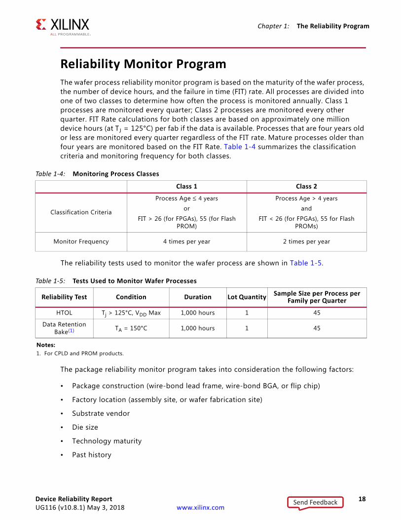
Reliability Monitor ProgramThe wafer process reliability monitor program is based on the maturity of the wafer process, the number of device hours, and the failure in time (FIT) rate. All processes are divided into one of two classes to determine how often the process is monitored annually. Class 1 processes are monitored every quarter; Class 2 processes are monitored every other quarter. FIT Rate calculations for both classes are based on approximately one million device hours (at TJ = 125°C) per fab if the data is available. Processes that are four years old or less are monitored every quarter regardless of the FIT rate. Mature processes older than four years are monitored based on the FIT Rate. Table 1-4 summarizes the classification criteria and monitoring frequency for both classes.
The reliability tests used to monitor the wafer process are shown in Table 1-5.
The package reliability monitor program takes into consideration the following factors:
• Package construction (wire-bond lead frame, wire-bond BGA, or flip chip)
• Factory location (assembly site, or wafer fabrication site)
• Substrate vendor
• Die size
• Technology maturity
• Past history
Table 1-4: Monitoring Process Classes
Class 1 Class 2
Classification Criteria
Process Age ≤ 4 years
or
FIT > 26 (for FPGAs), 55 (for Flash PROM)
Process Age > 4 years
and
FIT < 26 (for FPGAs), 55 for Flash PROMs)
Monitor Frequency 4 times per year 2 times per year
Table 1-5: Tests Used to Monitor Wafer Processes
Reliability Test Condition Duration Lot Quantity Sample Size per Process per Family per Quarter
HTOL Tj > 125°C, VDD Max 1,000 hours 1 45
Data Retention Bake(1) TA = 150°C 1,000 hours 1 45
Notes: 1. For CPLD and PROM products.
Device Reliability Report 18UG116 (v10.8.1) May 3, 2018 www.xilinx.com
Send Feedback
Chapter 1: The Reliability Program
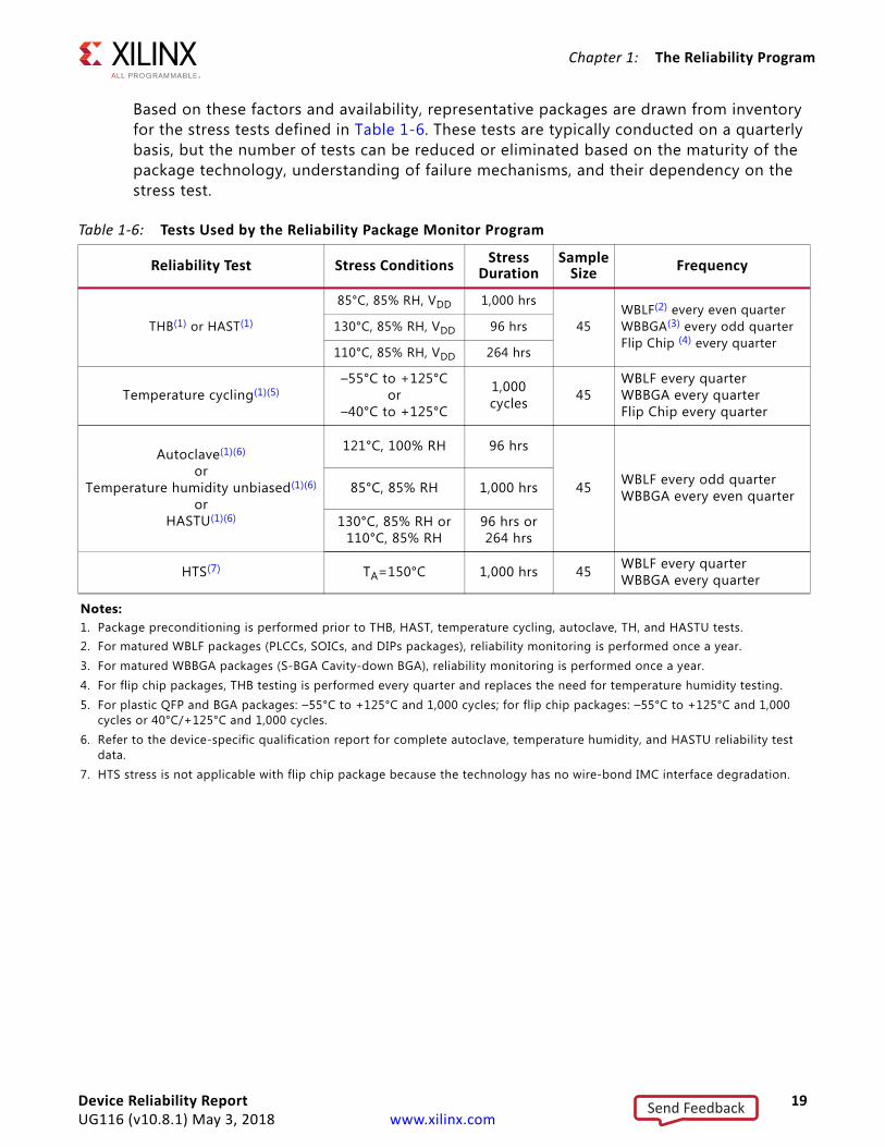
Based on these factors and availability, representative packages are drawn from inventory for the stress tests defined in Table 1-6. These tests are typically conducted on a quarterly basis, but the number of tests can be reduced or eliminated based on the maturity of the package technology, understanding of failure mechanisms, and their dependency on the stress test.
Table 1-6: Tests Used by the Reliability Package Monitor Program
Reliability Test Stress Conditions Stress Duration
Sample Size Frequency
THB(1) or HAST(1)
85°C, 85% RH, VDD 1,000 hrs
45WBLF(2) every even quarterWBBGA(3) every odd quarterFlip Chip (4) every quarter
130°C, 85% RH, VDD 96 hrs
110°C, 85% RH, VDD 264 hrs
Temperature cycling(1)(5)–55°C to +125°C
or–40°C to +125°C
1,000 cycles 45
WBLF every quarterWBBGA every quarterFlip Chip every quarter
Autoclave(1)(6)
or Temperature humidity unbiased(1)(6)
or HASTU(1)(6)
121°C, 100% RH 96 hrs
45 WBLF every odd quarterWBBGA every even quarter85°C, 85% RH 1,000 hrs
130°C, 85% RH or110°C, 85% RH
96 hrs or264 hrs
HTS(7) TA=150°C 1,000 hrs 45 WBLF every quarterWBBGA every quarter
Notes: 1. Package preconditioning is performed prior to THB, HAST, temperature cycling, autoclave, TH, and HASTU tests.2. For matured WBLF packages (PLCCs, SOICs, and DIPs packages), reliability monitoring is performed once a year.3. For matured WBBGA packages (S-BGA Cavity-down BGA), reliability monitoring is performed once a year.4. For flip chip packages, THB testing is performed every quarter and replaces the need for temperature humidity testing.5. For plastic QFP and BGA packages: –55°C to +125°C and 1,000 cycles; for flip chip packages: –55°C to +125°C and 1,000
cycles or 40°C/+125°C and 1,000 cycles.6. Refer to the device-specific qualification report for complete autoclave, temperature humidity, and HASTU reliability test
data.7. HTS stress is not applicable with flip chip package because the technology has no wire-bond IMC interface degradation.
Device Reliability Report 19UG116 (v10.8.1) May 3, 2018 www.xilinx.com
Send Feedback
Chapter 1: The Reliability Program
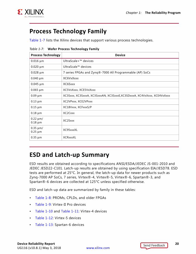
Process Technology FamilyTable 1-7 lists the Xilinx devices that support various process technologies.
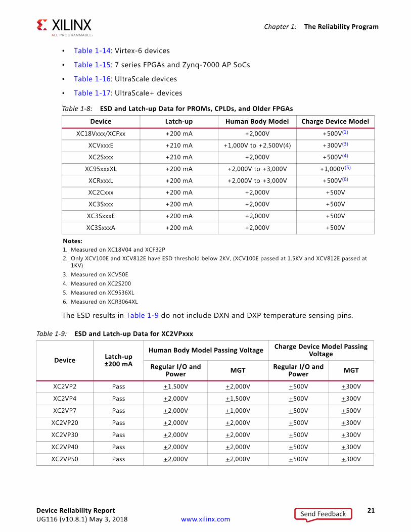
ESD and Latch-up SummaryESD results are obtained according to specifications ANSI/ESDA/JEDEC JS-001-2010 and JEDEC JESD22-C101. Latch-up results are obtained by using specification EIA/JESD78. ESD tests are performed at 25°C. In general, the latch-up data for newer products such as Zynq-7000 AP SoCs, 7 series, Virtex®-4, Virtex®-5, Virtex®-6, Spartan®-3, and Spartan®-6 devices are collected at 125°C unless specified otherwise.
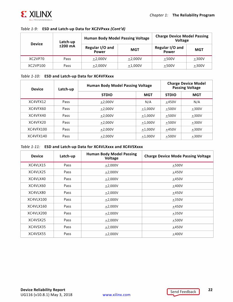
ESD and latch-up data are summarized by family in these tables:
• Table 1-8: PROMs, CPLDs, and older FPGAs
• Table 1-9: Virtex-II Pro devices
• Table 1-10 and Table 1-11: Virtex-4 devices
• Table 1-12: Virtex-5 devices
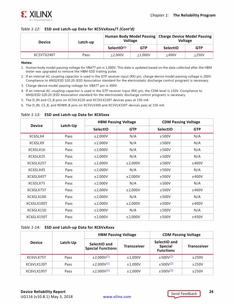
• Table 1-13: Spartan-6 devices
Table 1-7: Wafer Process Technology Family
Process Technology Device
0.016 μm UltraScale+™ devices
0.020 μm UltraScale™ devices
0.028 μm 7 series FPGAs and Zynq®-7000 All Programmable (AP) SoCs
0.040 μm XC6VxXxxx
0.045 μm XC6Sxxx
0.065 μm XC5VxXxxx, XCE5VxXxxx
0.09 μm XC3Sxxx, XC3SxxxA, XC3SxxxAN, XC3SxxxE,XC3SDxxxA, XC4VxXxxx, XCE4VxXxxx
0.13 μm XC2VPxxx, XCE2VPxxx
0.15 μm XC18Vxxx, XCFxxxS/P
0.18 μm XC2Cxxx
0.22 μm/0.18 μm XC2Sxxx
0.35 μm/0.25 μm XC95xxxXL
0.35 μm XCRxxxXL
Device Reliability Report 20UG116 (v10.8.1) May 3, 2018 www.xilinx.com
Send Feedback
Chapter 1: The Reliability Program
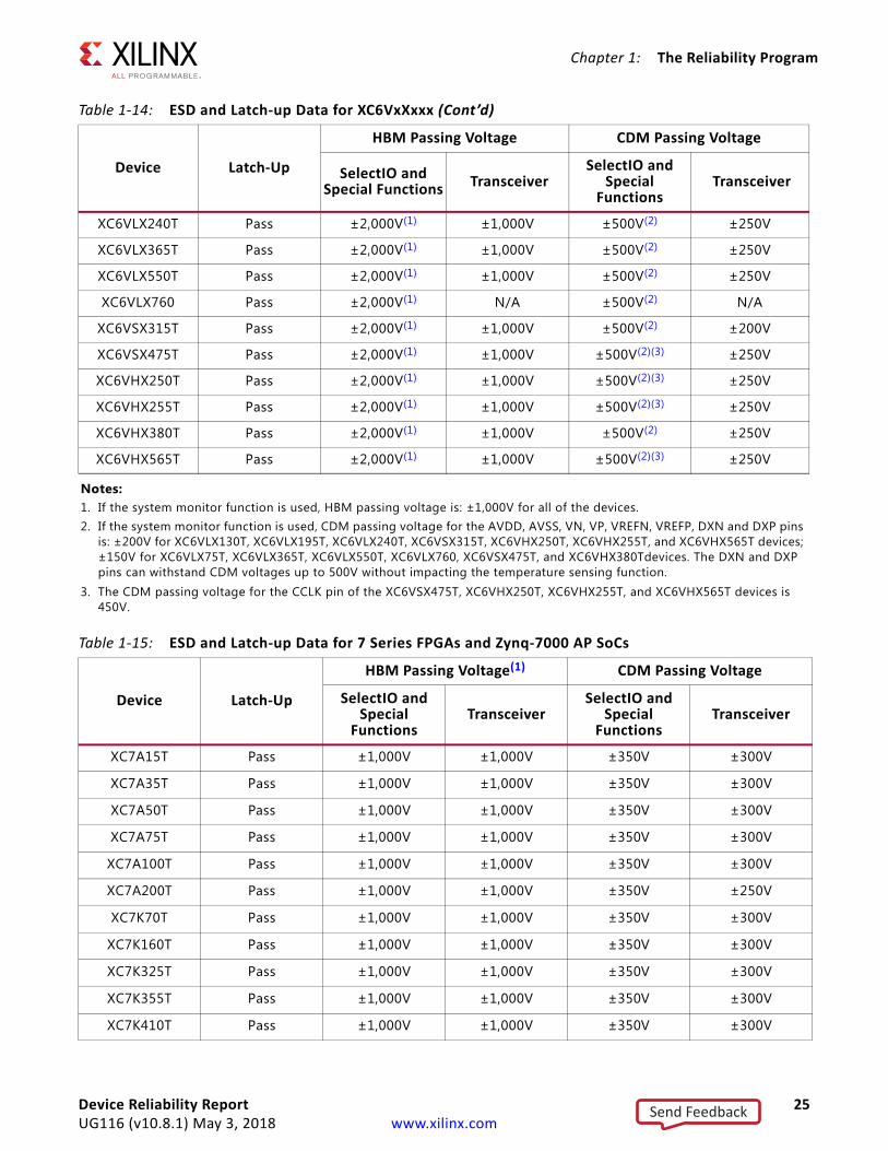
• Table 1-14: Virtex-6 devices
• Table 1-15: 7 series FPGAs and Zynq-7000 AP SoCs
• Table 1-16: UltraScale devices
• Table 1-17: UltraScale+ devicesM
The ESD results in Table 1-9 do not include DXN and DXP temperature sensing pins.
Table 1-8: ESD and Latch-up Data for PROMs, CPLDs, and Older FPGAs
Device Latch-up Human Body Model Charge Device Model
XC18Vxxx/XCFxx +200 mA +2,000V +500V(1)
XCVxxxE +210 mA +1,000V to +2,500V(4) +300V(3)
XC2Sxxx +210 mA +2,000V +500V(4)
XC95xxxXL +200 mA +2,000V to +3,000V +1,000V(5)
XCRxxxL +200 mA +2,000V to +3,000V +500V(6)
XC2Cxxx +200 mA +2,000V +500V
XC3Sxxx +200 mA +2,000V +500V
XC3SxxxE +200 mA +2,000V +500V
XC3SxxxA +200 mA +2,000V +500V
Notes: 1. Measured on XC18V04 and XCF32P2. Only XCV100E and XCV812E have ESD threshold below 2KV, (XCV100E passed at 1.5KV and XCV812E passed at
1KV)3. Measured on XCV50E4. Measured on XC2S2005. Measured on XC9536XL6. Measured on XCR3064XL
Table 1-9: ESD and Latch-up Data for XC2VPxxx
Device Latch-up ±200 mA
Human Body Model Passing Voltage Charge Device Model Passing Voltage
Regular I/O and Power MGT Regular I/O and
Power MGT
XC2VP2 Pass +1,500V +2,000V +500V +300V
XC2VP4 Pass +2,000V +1,500V +500V +300V
XC2VP7 Pass +2,000V +1,000V +500V +500V
XC2VP20 Pass +2,000V +2,000V +500V +300V
XC2VP30 Pass +2,000V +2,000V +500V +300V
XC2VP40 Pass +2,000V +2,000V +500V +300V
XC2VP50 Pass +2,000V +2,000V +500V +300V
Device Reliability Report 21UG116 (v10.8.1) May 3, 2018 www.xilinx.com
Send Feedback
Chapter 1: The Reliability Program
XC2VP70 Pass +2,000V +2,000V +500V +300V
XC2VP100 Pass +2,000V +1,000V +500V +300V
Table 1-9: ESD and Latch-up Data for XC2VPxxx (Cont’d)
Device Latch-up ±200 mA
Human Body Model Passing Voltage Charge Device Model Passing Voltage
Regular I/O and Power MGT Regular I/O and
Power MGT
Table 1-10: ESD and Latch-up Data for XC4VFXxxx
Device Latch-upHuman Body Model Passing Voltage Charge Device Model
Passing Voltage
STDIO MGT STDIO MGT
XC4VFX12 Pass +2,000V N/A +450V N/A
XC4VFX60 Pass +2,000V +1,000V +500V +300V
XC4VFX40 Pass +2,000V +1,000V +500V +300V
XC4VFX20 Pass +2,000V +1,000V +500V +300V
XC4VFX100 Pass +2,000V +1,000V +450V +300V
XC4VFX140 Pass +2,000V +1,000V +500V +300V
Table 1-11: ESD and Latch-up Data for XC4VLXxxx and XC4VSXxxx
Device Latch-up Human Body Model Passing Voltage Charge Device Mode Passing Voltage
XC4VLX15 Pass +2,000V +500V
XC4VLX25 Pass +2,000V +450V
XC4VLX40 Pass +2,000V +450V
XC4VLX60 Pass +2,000V +400V
XC4VLX80 Pass +2,000V +450V
XC4VLX100 Pass +2,000V +350V
XC4VLX160 Pass +2,000V +450V
XC4VLX200 Pass +2,000V +350V
XC4VSX25 Pass +2,000V +500V
XC4VSX35 Pass +2,000V +450V
XC4VSX55 Pass +2,000V +400V
Device Reliability Report 22UG116 (v10.8.1) May 3, 2018 www.xilinx.com
Send Feedback
Chapter 1: The Reliability Program
t
Table 1-12: ESD and Latch-up Data for XC5VxXxxx/T
Device Latch-upHuman Body Model Passing
VoltageCharge Device Model Passing
Voltage
SelectIO(1) GTP SelectIO GTP
XC5VLX20T Pass +2,000V +1,000V +400V +250V
XC5VLX30 Pass +2,000V N/A +400V N/A
XC5VLX30T Pass +2,000V +1,000V +400V +250V
XC5VLX50 Pass +2,000V N/A +400V N/A
XC5VLX50T Pass +2,000V +1,000V +400V +250V(2)
XC5VLX85 Pass +2,000V N/A +400V N/A
XC5VLX85T Pass +2,000V +1,000V +400V +250V(2)
XC5VLX110 Pass +2,000V N/A +400V(3) N/A
XC5VLX110T Pass +2,000V +1,000V +400V(3) +250V(2)
XC5VLX155 Pass +2,000V N/A +400V N/A
XC5VLX155T Pass +2,000V +1,000V +400V +250V(4)
XC5VLX220 Pass(5) +2,000V N/A +400V N/A
XC5VLX220T Pass(5) +2,000V +1,000V +400V +250V(4)
XC5VLX330 Pass(6) +2,000V N/A +400V N/A
XC5VLX330T Pass(6) +2,000V +1,000V +400V +250V(2)
XC5VFX30T Pass +2,000V +1,000V +400V +250V
XC5VFX70T Pass +2,000V +1,000V +400V +250V
XC5VFX100T Pass +2,000V +1,000V +400V +250V
XC5VFX130T Pass +2,000V +1,000V +400V +250V
XC5VFX200T Pass +2,000V +1,000V +400V +250V
XC5VSX35T Pass +2,000V +1,000V +400V +250V
XC5VSX50T Pass +2,000V +1,000V +400V +250V(2)
XC5VSX95T Pass +2,000V +1,000V +400V +250V
XC5VSX240T Pass +2,000V +1,000V +400V +250V(2)
XC5VTX150T Pass +2,000V +1,000V +400V +250V
Device Reliability Report 23UG116 (v10.8.1) May 3, 2018 www.xilinx.com
Send Feedback
Chapter 1: The Reliability Program
XC5VTX240T Pass +2,000V +1,000V +400V +250V
Notes: 1. Human body model passing voltage for VBATT pin is 1,000V. This data is updated based on the data collected after the HBM
tester was upgraded to remove the HBM-ESD trailing pulse.2. If an internal AC coupling capacitor is used in the GTP receiver input (RX) pin, charge device model passing voltage is 200V.
Compliance to ANSI/ESD S20.20 (ESD Association standard for the electrostatic discharge control program) is necessary.3. Charge device model passing voltage for VBATT pin is 300V.4. If an internal AC coupling capacitor is used in the GTP receiver input (RX) pin, the CDM level is 150V. Compliance to
ANSI/ESD S20.20 (ESD Association standard for the electrostatic discharge control program) is necessary.5. The D_IN and CS_B pins on XC5VLX220 and XC5VLX220T devices pass at 150 mA.6. The D_IN, CS_B, and RDWR_B pins on XC5VLX300 and XC5VLX330T devices pass at 150 mA.
Table 1-12: ESD and Latch-up Data for XC5VxXxxx/T (Cont’d)
Device Latch-upHuman Body Model Passing
VoltageCharge Device Model Passing
Voltage
SelectIO(1) GTP SelectIO GTP
Table 1-13: ESD and Latch-up Data for XC6Sxxx
Device Latch-UpHBM Passing Voltage CDM Passing Voltage
SelectIO GTP SelectIO GTP
XC6SLX4 Pass ±2,000V N/A ±500V N/A
XC6SLX9 Pass ±2,000V N/A ±500V N/A
XC6SLX16 Pass ±2,000V N/A ±500V N/A
XC6SLX25 Pass ±2,000V N/A ±500V N/A
XC6SLX25T Pass ±2,000V ±2,000V ±500V ±400V
XC6SLX45 Pass ±2,000V N/A ±500V N/A
XC6SLX45T Pass ±2,000V ±2,000V ±500V ±400V
XC6SLX75 Pass ±2,000V N/A ±500V N/A
XC6SLX75T Pass ±2,000V ±2,000V ±500V ±400V
XC6SLX100 Pass ±2,000V N/A ±500V N/A
XC6SLX100T Pass ±2,000V ±2,000V ±500V ±400V
XC6SLX150 Pass ±2,000V N/A ±500V N/A
XC6SLX150T Pass ±2,000V ±2,000V ±500V ±450V
Table 1-14: ESD and Latch-up Data for XC6VxXxxx
Device Latch-Up
HBM Passing Voltage CDM Passing Voltage
SelectIO and Special Functions Transceiver
SelectIO and Special
FunctionsTransceiver
XC6VLX75T Pass ±2,000V(1) ±1,000V ±500V(2) ±250V
XC6VLX130T Pass ±2,000V(1) ±1,000V ±500V(2) ±250V
XC6VLX195T Pass ±2,000V(1) ±1,000V ±500V(2) ±250V
Device Reliability Report 24UG116 (v10.8.1) May 3, 2018 www.xilinx.com
Send Feedback
Chapter 1: The Reliability Program
XC6VLX240T Pass ±2,000V(1) ±1,000V ±500V(2) ±250V
XC6VLX365T Pass ±2,000V(1) ±1,000V ±500V(2) ±250V
XC6VLX550T Pass ±2,000V(1) ±1,000V ±500V(2) ±250V
XC6VLX760 Pass ±2,000V(1) N/A ±500V(2) N/A
XC6VSX315T Pass ±2,000V(1) ±1,000V ±500V(2) ±200V
XC6VSX475T Pass ±2,000V(1) ±1,000V ±500V(2)(3) ±250V
XC6VHX250T Pass ±2,000V(1) ±1,000V ±500V(2)(3) ±250V
XC6VHX255T Pass ±2,000V(1) ±1,000V ±500V(2)(3) ±250V
XC6VHX380T Pass ±2,000V(1) ±1,000V ±500V(2) ±250V
XC6VHX565T Pass ±2,000V(1) ±1,000V ±500V(2)(3) ±250V
Notes: 1. If the system monitor function is used, HBM passing voltage is: ±1,000V for all of the devices.2. If the system monitor function is used, CDM passing voltage for the AVDD, AVSS, VN, VP, VREFN, VREFP, DXN and DXP pins
is: ±200V for XC6VLX130T, XC6VLX195T, XC6VLX240T, XC6VSX315T, XC6VHX250T, XC6VHX255T, and XC6VHX565T devices; ±150V for XC6VLX75T, XC6VLX365T, XC6VLX550T, XC6VLX760, XC6VSX475T, and XC6VHX380Tdevices. The DXN and DXP pins can withstand CDM voltages up to 500V without impacting the temperature sensing function.
3. The CDM passing voltage for the CCLK pin of the XC6VSX475T, XC6VHX250T, XC6VHX255T, and XC6VHX565T devices is 450V.
Table 1-14: ESD and Latch-up Data for XC6VxXxxx (Cont’d)
Device Latch-Up
HBM Passing Voltage CDM Passing Voltage
SelectIO and Special Functions Transceiver
SelectIO and Special
FunctionsTransceiver
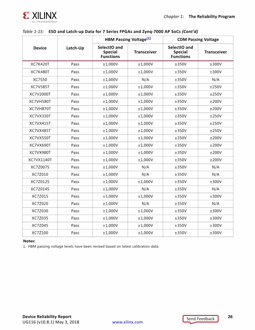
Table 1-15: ESD and Latch-up Data for 7 Series FPGAs and Zynq-7000 AP SoCs
Device Latch-Up
HBM Passing Voltage(1) CDM Passing Voltage
SelectIO and Special
FunctionsTransceiver
SelectIO and Special
FunctionsTransceiver
XC7A15T Pass ±1,000V ±1,000V ±350V ±300V
XC7A35T Pass ±1,000V ±1,000V ±350V ±300V
XC7A50T Pass ±1,000V ±1,000V ±350V ±300V
XC7A75T Pass ±1,000V ±1,000V ±350V ±300V
XC7A100T Pass ±1,000V ±1,000V ±350V ±300V
XC7A200T Pass ±1,000V ±1,000V ±350V ±250V
XC7K70T Pass ±1,000V ±1,000V ±350V ±300V
XC7K160T Pass ±1,000V ±1,000V ±350V ±300V
XC7K325T Pass ±1,000V ±1,000V ±350V ±300V
XC7K355T Pass ±1,000V ±1,000V ±350V ±300V
XC7K410T Pass ±1,000V ±1,000V ±350V ±300V
Device Reliability Report 25UG116 (v10.8.1) May 3, 2018 www.xilinx.com
Send Feedback
Chapter 1: The Reliability Program
XC7K420T Pass ±1,000V ±1,000V ±350V ±300V
XC7K480T Pass ±1,000V ±1,000V ±350V ±300V
XC7S50 Pass ±1,000V N/A ±350V N/A
XC7V585T Pass ±1,000V ±1,000V ±350V ±250V
XC7V2000T Pass ±1,000V ±1,000V ±350V ±250V
XC7VH580T Pass ±1,000V ±1,000V ±350V ±200V
XC7VH870T Pass ±1,000V ±1,000V ±350V ±200V
XC7VX330T Pass ±1,000V ±1,000V ±350V ±250V
XC7VX415T Pass ±1,000V ±1,000V ±350V ±250V
XC7VX485T Pass ±1,000V ±1,000V ±350V ±250V
XC7VX550T Pass ±1,000V ±1,000V ±350V ±200V
XC7VX690T Pass ±1,000V ±1,000V ±350V ±200V
XC7VX980T Pass ±1,000V ±1,000V ±350V ±200V
XC7VX1140T Pass ±1,000V ±1,000V ±350V ±200V
XC7Z007S Pass ±1,000V N/A ±350V N/A
XC7Z010 Pass ±1,000V N/A ±350V N/A
XC7Z012S Pass ±1,000V ±1,000V ±350V ±300V
XC7Z014S Pass ±1,000V N/A ±350V N/A
XC7Z015 Pass ±1,000V ±1,000V ±350V ±300V
XC7Z020 Pass ±1,000V N/A ±350V N/A
XC7Z030 Pass ±1,000V ±1,000V ±350V ±300V
XC7Z035 Pass ±1,000V ±1,000V ±350V ±300V
XC7Z045 Pass ±1,000V ±1,000V ±350V ±300V
XC7Z100 Pass ±1,000V ±1,000V ±350V ±300V
Notes: 1. HBM passing voltage levels have been revised based on latest calibration data.
Table 1-15: ESD and Latch-up Data for 7 Series FPGAs and Zynq-7000 AP SoCs (Cont’d)
Device Latch-Up
HBM Passing Voltage(1) CDM Passing Voltage
SelectIO and Special
FunctionsTransceiver
SelectIO and Special
FunctionsTransceiver
Device Reliability Report 26UG116 (v10.8.1) May 3, 2018 www.xilinx.com
Send Feedback
Chapter 1: The Reliability Program
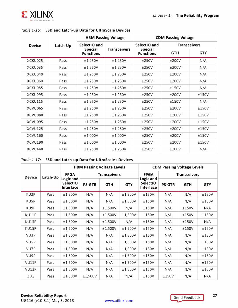
Table 1-16: ESD and Latch-up Data for UltraScale Devices
Device Latch-Up
HBM Passing Voltage CDM Passing Voltage
SelectIO and Special
FunctionsTransceivers
SelectIO and Special
Functions
Transceivers
GTH GTY
XCKU025 Pass ±1,250V ±1,250V ±250V ±200V N/A
XCKU035 Pass ±1,250V ±1,250V ±250V ±200V N/A
XCKU040 Pass ±1,250V ±1,250V ±250V ±200V N/A
XCKU060 Pass ±1,250V ±1,250V ±250V ±200V N/A
XCKU085 Pass ±1,250V ±1,250V ±250V ±150V N/A
XCKU095 Pass ±1,250V ±1,250V ±250V ±200V ±150V
XCKU115 Pass ±1,250V ±1,250V ±250V ±150V N/A
XCVU065 Pass ±1,250V ±1,250V ±250V ±200V ±150V
XCVU080 Pass ±1,250V ±1,250V ±250V ±200V ±150V
XCVU095 Pass ±1,250V ±1,250V ±250V ±200V ±150V
XCVU125 Pass ±1,250V ±1,250V ±250V ±200V ±150V
XCVU160 Pass ±1,000V ±1,000V ±250V ±200V ±150V
XCVU190 Pass ±1,000V ±1,000V ±250V ±200V ±150V
XCVU440 Pass ±1,250V ±1,250V ±250V ±200V N/A
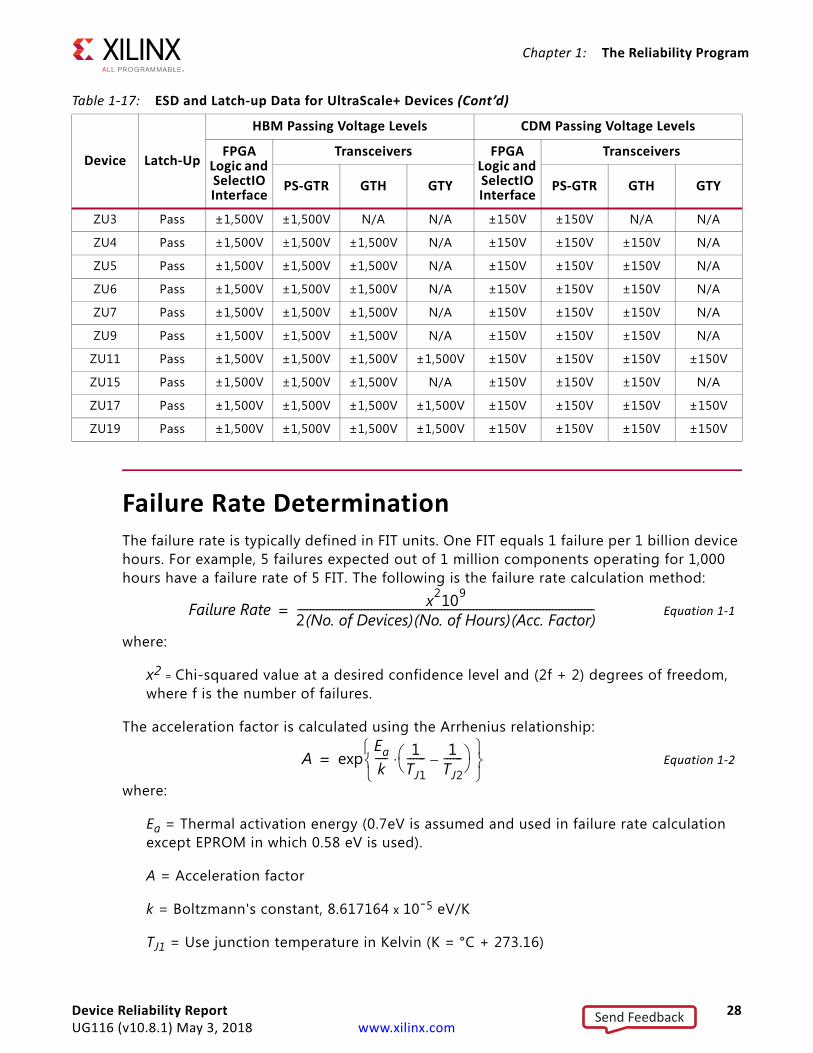
Table 1-17: ESD and Latch-up Data for UltraScale+ Devices
Device Latch-Up
HBM Passing Voltage Levels CDM Passing Voltage Levels
FPGA Logic and SelectIO Interface
Transceivers FPGA Logic and SelectIO Interface
Transceivers
PS-GTR GTH GTY PS-GTR GTH GTY
KU3P Pass ±1,500V N/A N/A ±1,500V ±150V N/A N/A ±150V
KU5P Pass ±1,500V N/A N/A ±1,500V ±150V N/A N/A ±150V
KU9P Pass ±1,500V N/A ±1,500V N/A ±150V N/A ±150V N/A
KU11P Pass ±1,500V N/A ±1,500V ±1,500V ±150V N/A ±150V ±150V
KU13P Pass ±1,500V N/A ±1,500V N/A ±150V N/A ±150V N/A
KU15P Pass ±1,500V N/A ±1,500V ±1,500V ±150V N/A ±150V ±150V
VU3P Pass ±1,500V N/A N/A ±1,500V ±150V N/A N/A ±150V
VU5P Pass ±1,500V N/A N/A ±1,500V ±150V N/A N/A ±150V
VU7P Pass ±1,500V N/A N/A ±1,500V ±150V N/A N/A ±150V
VU9P Pass ±1,500V N/A N/A ±1,500V ±150V N/A N/A ±150V
VU11P Pass ±1,500V N/A N/A ±1,500V ±150V N/A N/A ±150V
VU13P Pass ±1,500V N/A N/A ±1,500V ±150V N/A N/A ±150V
ZU2 Pass ±1,500V ±1,500V N/A N/A ±150V ±150V N/A N/A
Device Reliability Report 27UG116 (v10.8.1) May 3, 2018 www.xilinx.com
Send Feedback
Chapter 1: The Reliability Program
Failure Rate DeterminationThe failure rate is typically defined in FIT units. One FIT equals 1 failure per 1 billion device hours. For example, 5 failures expected out of 1 million components operating for 1,000 hours have a failure rate of 5 FIT. The following is the failure rate calculation method:
Equation 1-1
where:
x2 = Chi-squared value at a desired confidence level and (2f + 2) degrees of freedom, where f is the number of failures.
The acceleration factor is calculated using the Arrhenius relationship:
Equation 1-2
where:
Ea = Thermal activation energy (0.7eV is assumed and used in failure rate calculation except EPROM in which 0.58 eV is used).
A = Acceleration factor
k = Boltzmann's constant, 8.617164 x 10⁻⁵ eV/K
TJ1 = Use junction temperature in Kelvin (K = °C + 273.16)
ZU3 Pass ±1,500V ±1,500V N/A N/A ±150V ±150V N/A N/A
ZU4 Pass ±1,500V ±1,500V ±1,500V N/A ±150V ±150V ±150V N/A
ZU5 Pass ±1,500V ±1,500V ±1,500V N/A ±150V ±150V ±150V N/A
ZU6 Pass ±1,500V ±1,500V ±1,500V N/A ±150V ±150V ±150V N/A
ZU7 Pass ±1,500V ±1,500V ±1,500V N/A ±150V ±150V ±150V N/A
ZU9 Pass ±1,500V ±1,500V ±1,500V N/A ±150V ±150V ±150V N/A
ZU11 Pass ±1,500V ±1,500V ±1,500V ±1,500V ±150V ±150V ±150V ±150V
ZU15 Pass ±1,500V ±1,500V ±1,500V N/A ±150V ±150V ±150V N/A
ZU17 Pass ±1,500V ±1,500V ±1,500V ±1,500V ±150V ±150V ±150V ±150V
ZU19 Pass ±1,500V ±1,500V ±1,500V ±1,500V ±150V ±150V ±150V ±150V
Table 1-17: ESD and Latch-up Data for UltraScale+ Devices (Cont’d)
Device Latch-Up
HBM Passing Voltage Levels CDM Passing Voltage Levels
FPGA Logic and SelectIO Interface
Transceivers FPGA Logic and SelectIO Interface
Transceivers
PS-GTR GTH GTY PS-GTR GTH GTY
Failure Rate x2109
2(No. of Devices)(No. of Hours)(Acc. Factor)---------------------------------------------------------------------------------------------=
AEak---- 1
TJ1------ 1
TJ2------–
⋅
exp=
Device Reliability Report 28UG116 (v10.8.1) May 3, 2018 www.xilinx.com
Send Feedback
Chapter 1: The Reliability Program
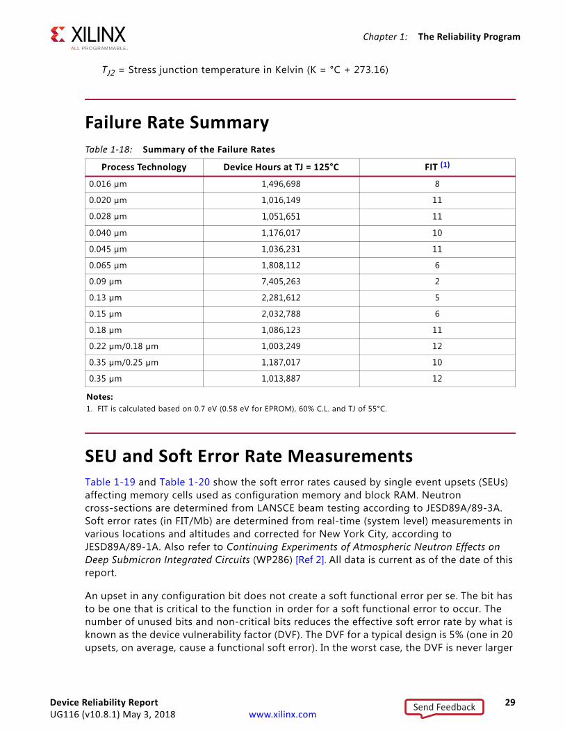
TJ2 = Stress junction temperature in Kelvin (K = °C + 273.16)
Failure Rate Summary
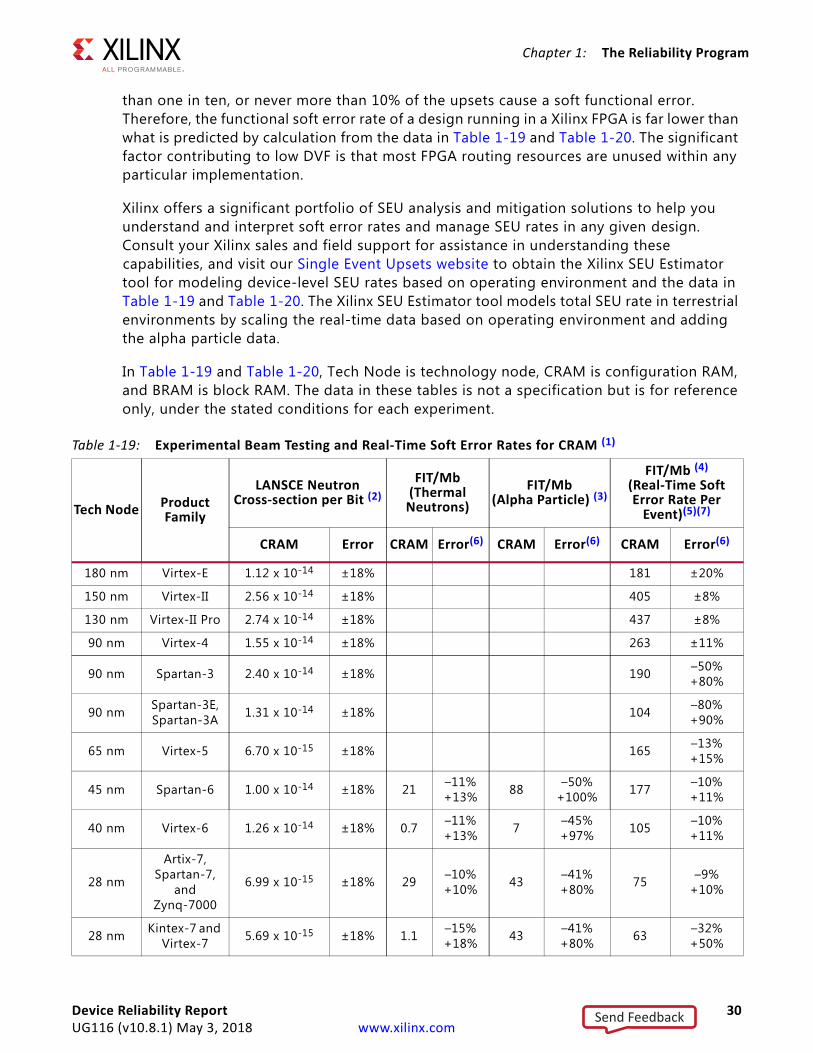
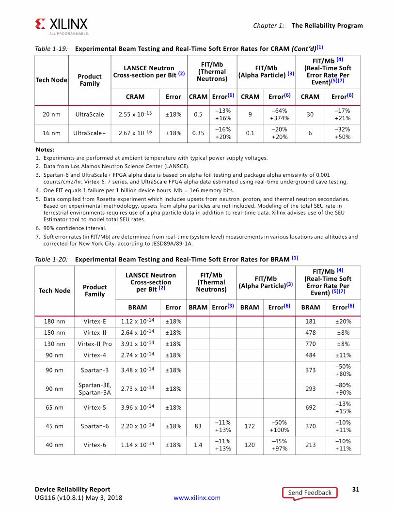
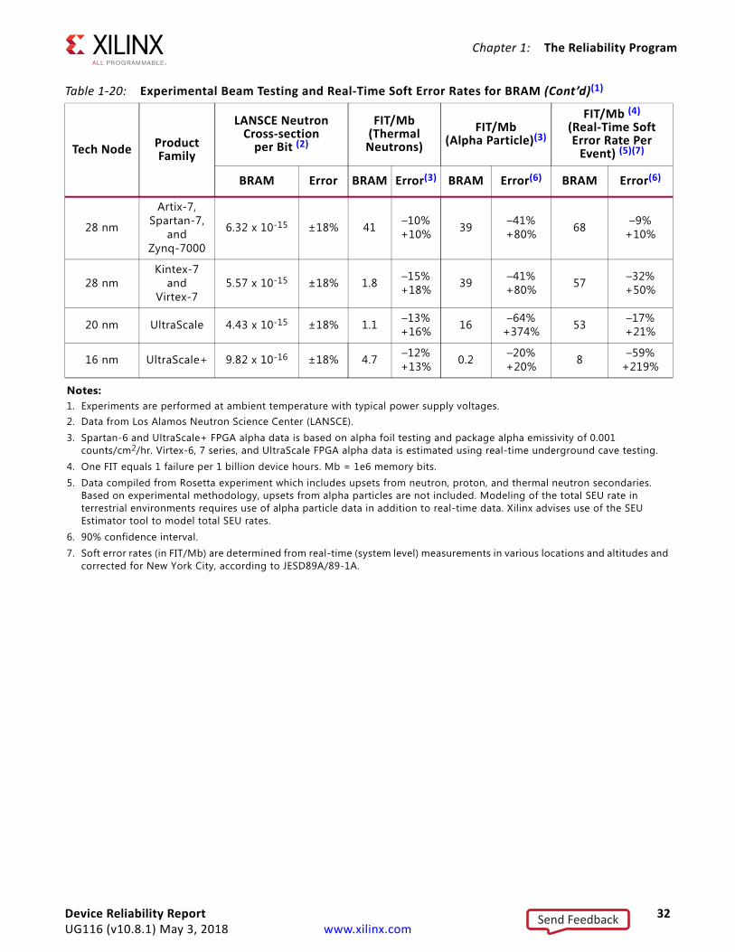
SEU and Soft Error Rate MeasurementsTable 1-19 and Table 1-20 show the soft error rates caused by single event upsets (SEUs) affecting memory cells used as configuration memory and block RAM. Neutron cross-sections are determined from LANSCE beam testing according to JESD89A/89-3A. Soft error rates (in FIT/Mb) are determined from real-time (system level) measurements in various locations and altitudes and corrected for New York City, according to JESD89A/89-1A. Also refer to Continuing Experiments of Atmospheric Neutron Effects on Deep Submicron Integrated Circuits (WP286) [Ref 2]. All data is current as of the date of this report.
An upset in any configuration bit does not create a soft functional error per se. The bit has to be one that is critical to the function in order for a soft functional error to occur. The number of unused bits and non-critical bits reduces the effective soft error rate by what is known as the device vulnerability factor (DVF). The DVF for a typical design is 5% (one in 20 upsets, on average, cause a functional soft error). In the worst case, the DVF is never larger
Table 1-18: Summary of the Failure Rates
Process Technology Device Hours at TJ = 125°C FIT (1)
0.016 µm 1,496,698 8
0.020 µm 1,016,149 11
0.028 µm 1,051,651 11
0.040 µm 1,176,017 10
0.045 µm 1,036,231 11
0.065 µm 1,808,112 6
0.09 µm 7,405,263 2
0.13 µm 2,281,612 5
0.15 µm 2,032,788 6
0.18 µm 1,086,123 11
0.22 µm/0.18 µm 1,003,249 12
0.35 µm/0.25 µm 1,187,017 10
0.35 µm 1,013,887 12
Notes: 1. FIT is calculated based on 0.7 eV (0.58 eV for EPROM), 60% C.L. and TJ of 55°C.
Device Reliability Report 29UG116 (v10.8.1) May 3, 2018 www.xilinx.com
Send Feedback
Chapter 1: The Reliability Program
than one in ten, or never more than 10% of the upsets cause a soft functional error. Therefore, the functional soft error rate of a design running in a Xilinx FPGA is far lower than what is predicted by calculation from the data in Table 1-19 and Table 1-20. The significant factor contributing to low DVF is that most FPGA routing resources are unused within any particular implementation.
Xilinx offers a significant portfolio of SEU analysis and mitigation solutions to help you understand and interpret soft error rates and manage SEU rates in any given design. Consult your Xilinx sales and field support for assistance in understanding these capabilities, and visit our Single Event Upsets website to obtain the Xilinx SEU Estimator tool for modeling device-level SEU rates based on operating environment and the data in Table 1-19 and Table 1-20. The Xilinx SEU Estimator tool models total SEU rate in terrestrial environments by scaling the real-time data based on operating environment and adding the alpha particle data.
In Table 1-19 and Table 1-20, Tech Node is technology node, CRAM is configuration RAM, and BRAM is block RAM. The data in these tables is not a specification but is for reference only, under the stated conditions for each experiment.
Table 1-19: Experimental Beam Testing and Real-Time Soft Error Rates for CRAM (1)
Tech Node Product Family
LANSCE Neutron Cross-section per Bit (2)
FIT/Mb (Thermal Neutrons)
FIT/Mb(Alpha Particle) (3)
FIT/Mb (4) (Real-Time Soft Error Rate Per
Event)(5)(7)
CRAM Error CRAM Error(6) CRAM Error(6) CRAM Error(6)
180 nm Virtex-E 1.12 x 10⁻¹⁴ ±18% 181 ±20%
150 nm Virtex-II 2.56 x 10⁻¹⁴ ±18% 405 ±8%
130 nm Virtex-II Pro 2.74 x 10⁻¹⁴ ±18% 437 ±8%
90 nm Virtex-4 1.55 x 10⁻¹⁴ ±18% 263 ±11%
90 nm Spartan-3 2.40 x 10⁻¹⁴ ±18% 190 –50%+80%
90 nm Spartan-3E, Spartan-3A 1.31 x 10⁻¹⁴ ±18% 104 –80%
+90%
65 nm Virtex-5 6.70 x 10⁻¹⁵ ±18% 165 –13%+15%
45 nm Spartan-6 1.00 x 10⁻¹⁴ ±18% 21 –11%+13% 88 –50%
+100% 177 –10%+11%
40 nm Virtex-6 1.26 x 10⁻¹⁴ ±18% 0.7 –11%+13% 7 –45%
+97% 105 –10%+11%
28 nm
Artix-7, Spartan-7,
and Zynq-7000
6.99 x 10⁻¹⁵ ±18% 29 –10%+10% 43 –41%
+80% 75 –9%+10%
28 nm Kintex-7 and Virtex-7 5.69 x 10⁻¹⁵ ±18% 1.1 –15%
+18% 43 –41%+80% 63 –32%
+50%
Device Reliability Report 30UG116 (v10.8.1) May 3, 2018 www.xilinx.com
Send Feedback
Chapter 1: The Reliability Program
20 nm UltraScale 2.55 x 10⁻¹⁵ ±18% 0.5 –13%+16% 9 –64%
+374% 30 –17%+21%
16 nm UltraScale+ 2.67 x 10⁻¹⁶ ±18% 0.35 –16%+20% 0.1 –20%
+20% 6 –32%+50%
Notes: 1. Experiments are performed at ambient temperature with typical power supply voltages.2. Data from Los Alamos Neutron Science Center (LANSCE).3. Spartan-6 and UltraScale+ FPGA alpha data is based on alpha foil testing and package alpha emissivity of 0.001
counts/cm2/hr. Virtex-6, 7 series, and UltraScale FPGA alpha data estimated using real-time underground cave testing.4. One FIT equals 1 failure per 1 billion device hours. Mb = 1e6 memory bits.5. Data compiled from Rosetta experiment which includes upsets from neutron, proton, and thermal neutron secondaries.
Based on experimental methodology, upsets from alpha particles are not included. Modeling of the total SEU rate in terrestrial environments requires use of alpha particle data in addition to real-time data. Xilinx advises use of the SEU Estimator tool to model total SEU rates.
6. 90% confidence interval.7. Soft error rates (in FIT/Mb) are determined from real-time (system level) measurements in various locations and altitudes and
corrected for New York City, according to JESD89A/89-1A.
Table 1-19: Experimental Beam Testing and Real-Time Soft Error Rates for CRAM (Cont’d)(1)
Tech Node Product Family
LANSCE Neutron Cross-section per Bit (2)
FIT/Mb (Thermal Neutrons)
FIT/Mb(Alpha Particle) (3)
FIT/Mb (4) (Real-Time Soft Error Rate Per
Event)(5)(7)
CRAM Error CRAM Error(6) CRAM Error(6) CRAM Error(6)
Table 1-20: Experimental Beam Testing and Real-Time Soft Error Rates for BRAM (1)
Tech Node Product Family
LANSCE Neutron Cross-section
per Bit (2)
FIT/Mb (Thermal Neutrons)
FIT/Mb(Alpha Particle)(3)
FIT/Mb (4) (Real-Time Soft Error Rate Per
Event) (5)(7)
BRAM Error BRAM Error(3) BRAM Error(6) BRAM Error(6)
180 nm Virtex-E 1.12 x 10⁻¹⁴ ±18% 181 ±20%
150 nm Virtex-II 2.64 x 10⁻¹⁴ ±18% 478 ±8%
130 nm Virtex-II Pro 3.91 x 10⁻¹⁴ ±18% 770 ±8%
90 nm Virtex-4 2.74 x 10⁻¹⁴ ±18% 484 ±11%
90 nm Spartan-3 3.48 x 10⁻¹⁴ ±18% 373 –50%+80%
90 nm Spartan-3E, Spartan-3A 2.73 x 10⁻¹⁴ ±18% 293 –80%
+90%
65 nm Virtex-5 3.96 x 10⁻¹⁴ ±18% 692 –13%+15%
45 nm Spartan-6 2.20 x 10⁻¹⁴ ±18% 83 –11%+13% 172 –50%
+100% 370 –10%+11%
40 nm Virtex-6 1.14 x 10⁻¹⁴ ±18% 1.4 –11%+13% 120 –45%
+97% 213 –10%+11%
Device Reliability Report 31UG116 (v10.8.1) May 3, 2018 www.xilinx.com
Send Feedback
Chapter 1: The Reliability Program
28 nm
Artix-7, Spartan-7,
and Zynq-7000
6.32 x 10⁻¹⁵ ±18% 41 –10%+10% 39 –41%
+80% 68 –9%+10%
28 nmKintex-7
and Virtex-7
5.57 x 10⁻¹⁵ ±18% 1.8 –15%+18% 39 –41%
+80% 57 –32%+50%
20 nm UltraScale 4.43 x 10⁻¹⁵ ±18% 1.1 –13%+16% 16 –64%
+374% 53 –17%+21%
16 nm UltraScale+ 9.82 x 10⁻¹⁶ ±18% 4.7 –12%+13% 0.2 –20%
+20% 8 –59%+219%
Notes: 1. Experiments are performed at ambient temperature with typical power supply voltages.2. Data from Los Alamos Neutron Science Center (LANSCE).3. Spartan-6 and UltraScale+ FPGA alpha data is based on alpha foil testing and package alpha emissivity of 0.001
counts/cm2/hr. Virtex-6, 7 series, and UltraScale FPGA alpha data is estimated using real-time underground cave testing.4. One FIT equals 1 failure per 1 billion device hours. Mb = 1e6 memory bits.5. Data compiled from Rosetta experiment which includes upsets from neutron, proton, and thermal neutron secondaries.
Based on experimental methodology, upsets from alpha particles are not included. Modeling of the total SEU rate in terrestrial environments requires use of alpha particle data in addition to real-time data. Xilinx advises use of the SEU Estimator tool to model total SEU rates.
6. 90% confidence interval.7. Soft error rates (in FIT/Mb) are determined from real-time (system level) measurements in various locations and altitudes and
corrected for New York City, according to JESD89A/89-1A.
Table 1-20: Experimental Beam Testing and Real-Time Soft Error Rates for BRAM (Cont’d)(1)
Tech Node Product Family
LANSCE Neutron Cross-section
per Bit (2)
FIT/Mb (Thermal Neutrons)
FIT/Mb(Alpha Particle)(3)
FIT/Mb (4) (Real-Time Soft Error Rate Per
Event) (5)(7)
BRAM Error BRAM Error(3) BRAM Error(6) BRAM Error(6)
Device Reliability Report 32UG116 (v10.8.1) May 3, 2018 www.xilinx.com
Send Feedback
Chapter 2
Results by Product Family
FPGA Products
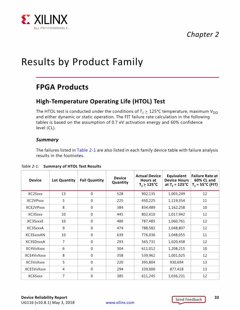
High-Temperature Operating Life (HTOL) TestThe HTOL test is conducted under the conditions of TJ > 125°C temperature, maximum VDD and either dynamic or static operation. The FIT failure rate calculation in the following tables is based on the assumption of 0.7 eV activation energy and 60% confidence level (CL).
Summary
The failures listed in Table 2-1 are also listed in each family device table with failure analysis results in the footnotes.
Table 2-1: Summary of HTOL Test Results
Device Lot Quantity Fail Quantity Device Quantity
Actual Device Hours at
TJ > 125°C
Equivalent Device Hours at TJ = 125°C
Failure Rate at 60% CL and
TJ = 55°C (FIT)
XC2Sxxx 13 0 528 902,135 1,003,249 12
XC2VPxxx 5 0 225 450,225 1,119,354 11
XCE2VPxxx 8 0 384 834,489 1,162,258 10
XC3Sxxx 10 0 445 802,610 1,017,942 12
XC3SxxxE 10 0 480 787,485 1,060,761 12
XC3SxxxA 9 0 474 788,582 1,048,807 12
XC3SxxxAN 10 0 639 776,036 1,048,055 11
XC3SDxxxA 7 0 293 565,731 1,020,458 12
XC4VxXxxx 6 0 304 611,012 1,208,215 10
XCE4VxXxxx 8 0 358 539,962 1,001,025 12
XC5VxXxxx 5 0 220 395,804 930,694 13
XCE5VxXxxx 4 0 294 339,000 877,418 13
XC6Sxxx 7 0 385 611,245 1,036,231 12
Device Reliability Report 33UG116 (v10.8.1) May 3, 2018 www.xilinx.com
Send Feedback
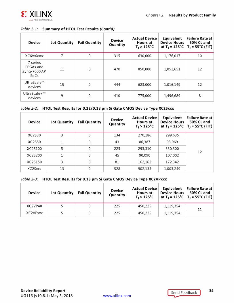
Chapter 2: Results by Product Family
XC6VxXxxx 7 0 315 630,000 1,176,017 10
7 series FPGAs and
Zynq-7000 AP SoCs
11 0 470 850,000 1,051,651 12
UltraScale™ devices 15 0 444 623,000 1,016,149 12
UltraScale+™ devices 9 0 410 775,000 1,496,689 8
Table 2-1: Summary of HTOL Test Results (Cont’d)
Device Lot Quantity Fail Quantity Device Quantity
Actual Device Hours at
TJ > 125°C
Equivalent Device Hours at TJ = 125°C
Failure Rate at 60% CL and
TJ = 55°C (FIT)
Table 2-2: HTOL Test Results for 0.22/0.18 µm Si Gate CMOS Device Type XC2Sxxx
Device Lot Quantity Fail Quantity Device Quantity
Actual Device Hours at
TJ > 125°C
Equivalent Device Hours at TJ = 125°C
Failure Rate at 60% CL and
TJ = 55°C (FIT)
XC2S30 3 0 134 270,186 299,635
12
XC2S50 1 0 43 86,387 93,969
XC2S100 5 0 225 293,310 330,300
XC2S200 1 0 45 90,090 107,002
XC2S150 3 0 81 162,162 172,342
XC2Sxxx 13 0 528 902,135 1,003,249
Table 2-3: HTOL Test Results for 0.13 µm Si Gate CMOS Device Type XC2VPxxx
Device Lot Quantity Fail Quantity Device Quantity
Actual Device Hours at
TJ > 125°C
Equivalent Device Hours at TJ = 125°C
Failure Rate at 60% CL and
TJ = 55°C (FIT)
XC2VP40 5 0 225 450,225 1,119,35411
XC2VPxxx 5 0 225 450,225 1,119,354
Device Reliability Report 34UG116 (v10.8.1) May 3, 2018 www.xilinx.com
Send Feedback
Chapter 2: Results by Product Family
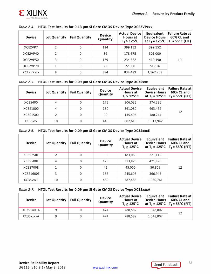
Table 2-4: HTOL Test Results for 0.13 µm Si Gate CMOS Device Type XCE2VPxxx
Device Lot Quantity Fail Quantity Device Quantity
Actual Device Hours at
TJ > 125°C
Equivalent Device Hours at TJ = 125°C
Failure Rate at 60% CL and
TJ = 55°C (FIT)
XCE2VP7 2 0 134 399,152 399,152
10
XCE2VP40 2 0 89 178,675 301,000
XCE2VP50 3 0 139 234,662 410,490
XCE2VP70 1 0 22 22,000 51,616
XCE2VPxxx 8 0 384 834,489 1,162,258
Table 2-5: HTOL Test Results for 0.09 µm Si Gate CMOS Device Type XC3Sxxx
Device Lot Quantity Fail Quantity Device Quantity
Actual Device Hours at
TJ > 125°C
Equivalent Device Hours at TJ = 125°C
Failure Rate at 60% CL and
TJ = 55°C (FIT)
XC3S400 4 0 175 306,035 374,236
12XC3S1000 4 0 180 361,080 463,462
XC3S1500 2 0 90 135,495 180,244
XC3Sxxx 10 0 445 802,610 1,017,942
Table 2-6: HTOL Test Results for 0.09 µm Si Gate CMOS Device Type XC3SxxxE
Device Lot Quantity Fail Quantity Device Quantity
Actual Device Hours at
TJ > 125°C
Equivalent Device Hours at TJ = 125°C
Failure Rate at 60% CL and
TJ = 55°C (FIT)
XC3S250E 2 0 90 183,060 221,112
12
XC3S500E 4 0 178 313,820 421,895
XC3S700E 1 0 45 45,000 50,809
XC3S1600E 3 0 167 245,605 366,945
XC3SxxxE 10 0 480 787,485 1,060,761
Table 2-7: HTOL Test Results for 0.09 µm Si Gate CMOS Device Type XC3SxxxA
Device Lot Quantity Fail Quantity Device Quantity
Actual Device Hours at
TJ > 125°C
Equivalent Device Hours at TJ = 125°C
Failure Rate at 60% CL and
TJ = 55°C (FIT)
XC3S1400A 9 0 474 788,582 1,048,80712
XC3SxxxxA 9 0 474 788,582 1,048,807
Device Reliability Report 35UG116 (v10.8.1) May 3, 2018 www.xilinx.com
Send Feedback
Chapter 2: Results by Product Family
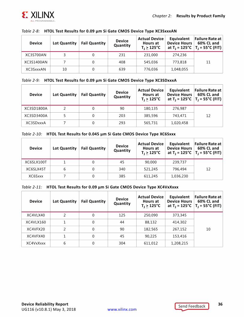
Table 2-8: HTOL Test Results for 0.09 µm Si Gate CMOS Device Type XC3SxxxAN
Device Lot Quantity Fail Quantity Device Quantity
Actual Device Hours at
TJ > 125°C
Equivalent Device Hours at TJ = 125°C
Failure Rate at 60% CL and
TJ = 55°C (FIT)
XC3S700AN 3 0 231 231,000 274,236
11XC3S1400AN 7 0 408 545,036 773,818
XC3SxxxAN 10 0 639 776,036 1,048,055
Table 2-9: HTOL Test Results for 0.09 µm Si Gate CMOS Device Type XC3SDxxxA
Device Lot Quantity Fail Quantity Device Quantity
Actual Device Hours at
TJ > 125°C
Equivalent Device Hours at TJ = 125°C
Failure Rate at 60% CL and
TJ = 55°C (FIT)
XC3SD1800A 2 0 90 180,135 276,987
12XC3SD3400A 5 0 203 385,596 743,471
XC3SDxxxA 7 0 293 565,731 1,020,458
Table 2-10: HTOL Test Results for 0.045 µm Si Gate CMOS Device Type XC6Sxxx
Device Lot Quantity Fail Quantity Device Quantity
Actual Device Hours at
TJ > 125°C
Equivalent Device Hours at TJ = 125°C
Failure Rate at 60% CL and
TJ = 55°C (FIT)
XC6SLX100T 1 0 45 90,000 239,737
12XC6SLX45T 6 0 340 521,245 796,494
XC6Sxxx 7 0 385 611,245 1,036,230
Table 2-11: HTOL Test Results for 0.09 µm Si Gate CMOS Device Type XC4VxXxxx
Device Lot Quantity Fail Quantity Device Quantity
Actual Device Hours at
TJ > 125°C
Equivalent Device Hours at TJ = 125°C
Failure Rate at 60% CL and
TJ = 55°C (FIT)
XC4VLX40 2 0 125 250,090 373,345
10
XC4VLX160 1 0 44 88,132 414,302
XC4VFX20 2 0 90 182,565 267,152
XC4VFX40 1 0 45 90,225 153,416
XC4VxXxxx 6 0 304 611,012 1,208,215
Device Reliability Report 36UG116 (v10.8.1) May 3, 2018 www.xilinx.com
Send Feedback
Chapter 2: Results by Product Family
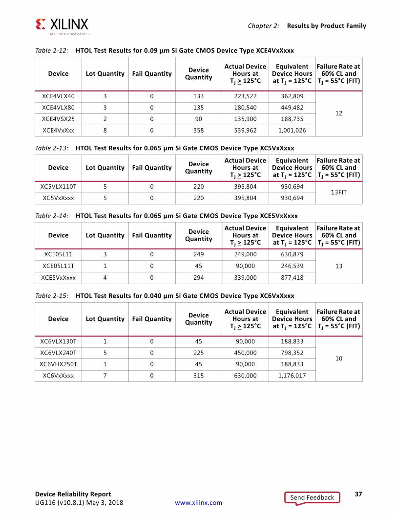
Table 2-12: HTOL Test Results for 0.09 µm Si Gate CMOS Device Type XCE4VxXxxx
Device Lot Quantity Fail Quantity Device Quantity
Actual Device Hours at
TJ > 125°C
Equivalent Device Hours at TJ = 125°C
Failure Rate at 60% CL and
TJ = 55°C (FIT)
XCE4VLX40 3 0 133 223,522 362,809
12XCE4VLX80 3 0 135 180,540 449,482
XCE4VSX25 2 0 90 135,900 188,735
XCE4VxXxx 8 0 358 539,962 1,001,026
Table 2-13: HTOL Test Results for 0.065 µm Si Gate CMOS Device Type XC5VxXxxx
Device Lot Quantity Fail Quantity Device Quantity
Actual Device Hours at
TJ > 125°C
Equivalent Device Hours at TJ = 125°C
Failure Rate at 60% CL and
TJ = 55°C (FIT)
XC5VLX110T 5 0 220 395,804 930,69413FIT
XC5VxXxxx 5 0 220 395,804 930,694
Table 2-14: HTOL Test Results for 0.065 µm Si Gate CMOS Device Type XCE5VxXxxx
Device Lot Quantity Fail Quantity Device Quantity
Actual Device Hours at
TJ > 125°C
Equivalent Device Hours at TJ = 125°C
Failure Rate at 60% CL and
TJ = 55°C (FIT)
XCE05L11 3 0 249 249,000 630,879
13XCE05L11T 1 0 45 90,000 246,539
XCE5VxXxxx 4 0 294 339,000 877,418
Table 2-15: HTOL Test Results for 0.040 µm Si Gate CMOS Device Type XC6VxXxxx
Device Lot Quantity Fail Quantity Device Quantity
Actual Device Hours at
TJ > 125°C
Equivalent Device Hours at TJ = 125°C
Failure Rate at 60% CL and
TJ = 55°C (FIT)
XC6VLX130T 1 0 45 90,000 188,833
10XC6VLX240T 5 0 225 450,000 798,352
XC6VHX250T 1 0 45 90,000 188,833
XC6VxXxxx 7 0 315 630,000 1,176,017
Device Reliability Report 37UG116 (v10.8.1) May 3, 2018 www.xilinx.com
Send Feedback
Chapter 2: Results by Product Family
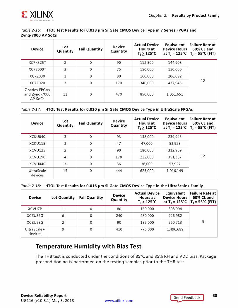
Temperature Humidity with Bias TestThe THB test is conducted under the conditions of 85°C and 85% RH and VDD bias. Package preconditioning is performed on the testing samples prior to the THB test.
Table 2-16: HTOL Test Results for 0.028 µm Si Gate CMOS Device Type in 7 Series FPGAs and Zynq-7000 AP SoCs
Device Lot Quantity Fail Quantity Device
QuantityActual Device
Hours at TJ > 125°C
Equivalent Device Hours at TJ = 125°C
Failure Rate at 60% CL and
TJ = 55°C (FIT)
XC7K325T 2 0 90 112,500 144,908
12
XC72000T 3 0 75 150,000 150,000
XC7Z030 1 0 80 160,000 206,092
XC7Z020 3 0 170 340,000 437,945
7 series FPGAs and Zynq-7000
AP SoCs11 0 470 850,000 1,051,651
Table 2-17: HTOL Test Results for 0.020 µm Si Gate CMOS Device Type in UltraScale FPGAs
Device Lot Quantity Fail Quantity Device
QuantityActual Device
Hours at TJ > 125°C
Equivalent Device Hours at TJ = 125°C
Failure Rate at 60% CL and
TJ = 55°C (FIT)
XCKU040 3 0 93 138,000 239,943
12
XCKU115 3 0 47 47,000 53,923
XCVU125 2 0 90 180,000 312,969
XCVU190 4 0 178 222,000 351,387
XCVU440 3 0 36 36,000 57,927
UltraScale devices
15 0 444 623,000 1,016,149
Table 2-18: HTOL Test Results for 0.016 μm Si Gate CMOS Device Type in the UltraScale+ Family
Device Lot Quantity Fail Quantity Device Quantity
Actual Device Hours at
TJ > 125°C
Equivalent Device Hours at TJ = 125°C
Failure Rate at 60% CL and
TJ = 55°C (FIT)
XCVU7P 1 0 80 160,000 308,994
8XCZU3EG 6 0 240 480,000 926,982
XCZU9EG 2 0 90 135,000 260,713
UltraScale+ devices
9 0 410 775,000 1,496,689
Device Reliability Report 38UG116 (v10.8.1) May 3, 2018 www.xilinx.com
Send Feedback
Chapter 2: Results by Product Family
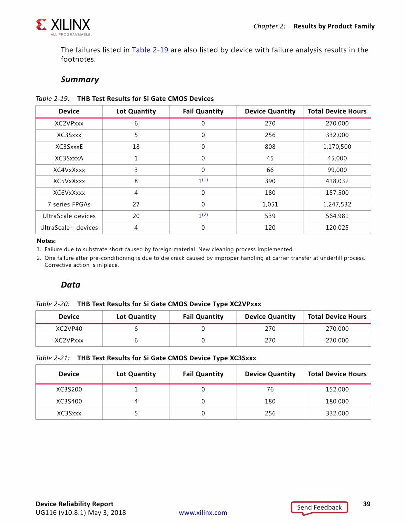
The failures listed in Table 2-19 are also listed by device with failure analysis results in the footnotes.
Summary
Data
Table 2-19: THB Test Results for Si Gate CMOS Devices
Device Lot Quantity Fail Quantity Device Quantity Total Device Hours
XC2VPxxx 6 0 270 270,000
XC3Sxxx 5 0 256 332,000
XC3SxxxE 18 0 808 1,170,500
XC3SxxxA 1 0 45 45,000
XC4VxXxxx 3 0 66 99,000
XC5VxXxxx 8 1(1) 390 418,032
XC6VxXxxx 4 0 180 157,500
7 series FPGAs 27 0 1,051 1,247,532
UltraScale devices 20 1(2) 539 564,981
UltraScale+ devices 4 0 120 120,025
Notes: 1. Failure due to substrate short caused by foreign material. New cleaning process implemented.2. One failure after pre-conditioning is due to die crack caused by improper handling at carrier transfer at underfill process.
Corrective action is in place.
Table 2-20: THB Test Results for Si Gate CMOS Device Type XC2VPxxx
Device Lot Quantity Fail Quantity Device Quantity Total Device Hours
XC2VP40 6 0 270 270,000
XC2VPxxx 6 0 270 270,000
Table 2-21: THB Test Results for Si Gate CMOS Device Type XC3Sxxx
Device Lot Quantity Fail Quantity Device Quantity Total Device Hours
XC3S200 1 0 76 152,000
XC3S400 4 0 180 180,000
XC3Sxxx 5 0 256 332,000
Device Reliability Report 39UG116 (v10.8.1) May 3, 2018 www.xilinx.com
Send Feedback
Chapter 2: Results by Product Family
N
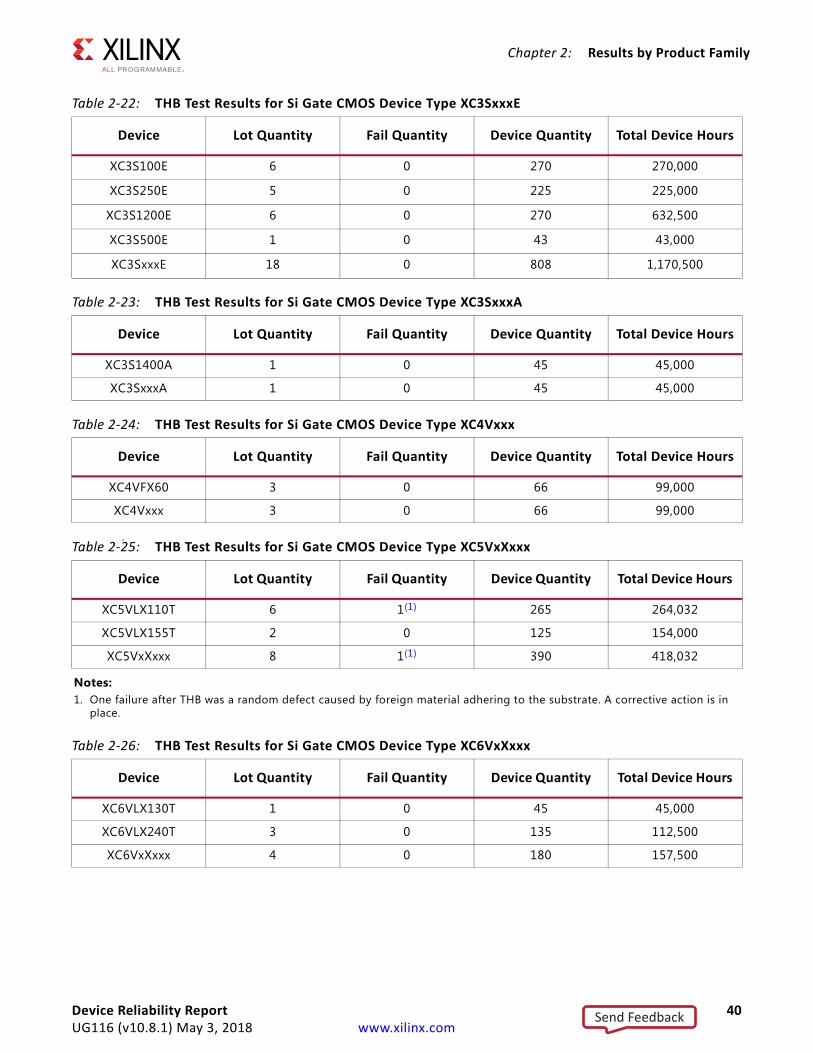
Table 2-22: THB Test Results for Si Gate CMOS Device Type XC3SxxxE
Device Lot Quantity Fail Quantity Device Quantity Total Device Hours
XC3S100E 6 0 270 270,000
XC3S250E 5 0 225 225,000
XC3S1200E 6 0 270 632,500
XC3S500E 1 0 43 43,000
XC3SxxxE 18 0 808 1,170,500
Table 2-23: THB Test Results for Si Gate CMOS Device Type XC3SxxxA
Device Lot Quantity Fail Quantity Device Quantity Total Device Hours
XC3S1400A 1 0 45 45,000
XC3SxxxA 1 0 45 45,000
Table 2-24: THB Test Results for Si Gate CMOS Device Type XC4Vxxx
Device Lot Quantity Fail Quantity Device Quantity Total Device Hours
XC4VFX60 3 0 66 99,000
XC4Vxxx 3 0 66 99,000
Table 2-25: THB Test Results for Si Gate CMOS Device Type XC5VxXxxx
Device Lot Quantity Fail Quantity Device Quantity Total Device Hours
XC5VLX110T 6 1(1) 265 264,032
XC5VLX155T 2 0 125 154,000
XC5VxXxxx 8 1(1) 390 418,032
Notes: 1. One failure after THB was a random defect caused by foreign material adhering to the substrate. A corrective action is in
place.
Table 2-26: THB Test Results for Si Gate CMOS Device Type XC6VxXxxx
Device Lot Quantity Fail Quantity Device Quantity Total Device Hours
XC6VLX130T 1 0 45 45,000
XC6VLX240T 3 0 135 112,500
XC6VxXxxx 4 0 180 157,500
Device Reliability Report 40UG116 (v10.8.1) May 3, 2018 www.xilinx.com
Send Feedback
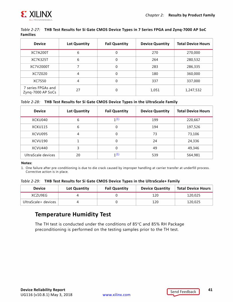
Chapter 2: Results by Product Family
Temperature Humidity TestThe TH test is conducted under the conditions of 85°C and 85% RH Package preconditioning is performed on the testing samples prior to the TH test.
Table 2-27: THB Test Results for Si Gate CMOS Device Types in 7 Series FPGA and Zynq-7000 AP SoC Families
Device Lot Quantity Fail Quantity Device Quantity Total Device Hours
XC7A200T 6 0 270 270,000
XC7K325T 6 0 264 280,532
XC7V2000T 7 0 283 286,335
XC7Z020 4 0 180 360,000
XC7S50 4 0 337 337,000
7 series FPGAs and Zynq-7000 AP SoCs 27 0 1,051 1,247,532
Table 2-28: THB Test Results for Si Gate CMOS Device Types in the UltraScale Family
Device Lot Quantity Fail Quantity Device Quantity Total Device Hours
XCKU040 6 1(1) 199 220,667
XCKU115 6 0 194 197,526
XCVU095 4 0 73 73,106
XCVU190 1 0 24 24,336
XCVU440 3 0 49 49,346
UltraScale devices 20 1(1) 539 564,981
Notes: 1. One failure after pre-conditioning is due to die crack caused by improper handling at carrier transfer at underfill process.
Corrective action is in place.
Table 2-29: THB Test Results for Si Gate CMOS Device Types in the UltraScale+ Family
Device Lot Quantity Fail Quantity Device Quantity Total Device Hours
XCZU9EG 4 0 120 120,025
UltraScale+ devices 4 0 120 120,025
Device Reliability Report 41UG116 (v10.8.1) May 3, 2018 www.xilinx.com
Send Feedback
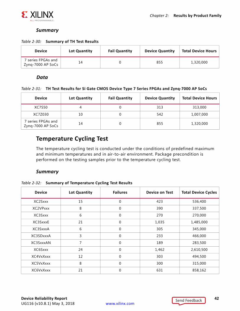
Chapter 2: Results by Product Family
Summary
Data
Temperature Cycling TestThe temperature cycling test is conducted under the conditions of predefined maximum and minimum temperatures and in air-to-air environment. Package precondition is performed on the testing samples prior to the temperature cycling test.
Summary
Table 2-30: Summary of TH Test Results
Device Lot Quantity Fail Quantity Device Quantity Total Device Hours
7 series FPGAs and Zynq-7000 AP SoCs 14 0 855 1,320,000
Table 2-31: TH Test Results for Si Gate CMOS Device Type 7 Series FPGAs and Zynq-7000 AP SoCs
Device Lot Quantity Fail Quantity Device Quantity Total Device Hours
XC7S50 4 0 313 313,000
XC7Z030 10 0 542 1,007,000
7 series FPGAs and Zynq-7000 AP SoCs 14 0 855 1,320,000
Table 2-32: Summary of Temperature Cycling Test Results
Device Lot Quantity Failures Device on Test Total Device Cycles
XC2Sxxx 15 0 423 536,400
XC2VPxxx 8 0 390 337,500
XC3Sxxx 6 0 270 270,000
XC3SxxxE 21 0 1,035 1,485,000
XC3SxxxA 6 0 305 345,000
XC3SDxxxA 3 0 233 466,000
XC3SxxxAN 7 0 189 283,500
XC6Sxxx 24 0 1,462 2,610,500
XC4VxXxxx 12 0 303 494,500
XC5VxXxxx 8 0 300 315,000
XC6VxXxxx 21 0 631 858,162
Device Reliability Report 42UG116 (v10.8.1) May 3, 2018 www.xilinx.com
Send Feedback
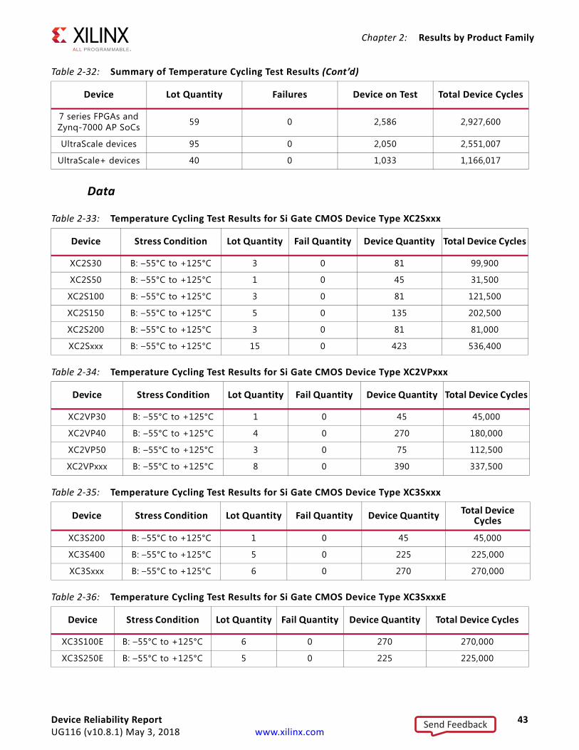
Chapter 2: Results by Product Family
Data
7 series FPGAs and Zynq-7000 AP SoCs 59 0 2,586 2,927,600
UltraScale devices 95 0 2,050 2,551,007
UltraScale+ devices 40 0 1,033 1,166,017
Table 2-32: Summary of Temperature Cycling Test Results (Cont’d)
Device Lot Quantity Failures Device on Test Total Device Cycles
Table 2-33: Temperature Cycling Test Results for Si Gate CMOS Device Type XC2Sxxx
Device Stress Condition Lot Quantity Fail Quantity Device Quantity Total Device Cycles
XC2S30 B: –55°C to +125°C 3 0 81 99,900
XC2S50 B: –55°C to +125°C 1 0 45 31,500
XC2S100 B: –55°C to +125°C 3 0 81 121,500
XC2S150 B: –55°C to +125°C 5 0 135 202,500
XC2S200 B: –55°C to +125°C 3 0 81 81,000
XC2Sxxx B: –55°C to +125°C 15 0 423 536,400
Table 2-34: Temperature Cycling Test Results for Si Gate CMOS Device Type XC2VPxxx
Device Stress Condition Lot Quantity Fail Quantity Device Quantity Total Device Cycles
XC2VP30 B: –55°C to +125°C 1 0 45 45,000
XC2VP40 B: –55°C to +125°C 4 0 270 180,000
XC2VP50 B: –55°C to +125°C 3 0 75 112,500
XC2VPxxx B: –55°C to +125°C 8 0 390 337,500
Table 2-35: Temperature Cycling Test Results for Si Gate CMOS Device Type XC3Sxxx
Device Stress Condition Lot Quantity Fail Quantity Device Quantity Total Device Cycles
XC3S200 B: –55°C to +125°C 1 0 45 45,000
XC3S400 B: –55°C to +125°C 5 0 225 225,000
XC3Sxxx B: –55°C to +125°C 6 0 270 270,000
Table 2-36: Temperature Cycling Test Results for Si Gate CMOS Device Type XC3SxxxE
Device Stress Condition Lot Quantity Fail Quantity Device Quantity Total Device Cycles
XC3S100E B: –55°C to +125°C 6 0 270 270,000
XC3S250E B: –55°C to +125°C 5 0 225 225,000
Device Reliability Report 43UG116 (v10.8.1) May 3, 2018 www.xilinx.com
Send Feedback
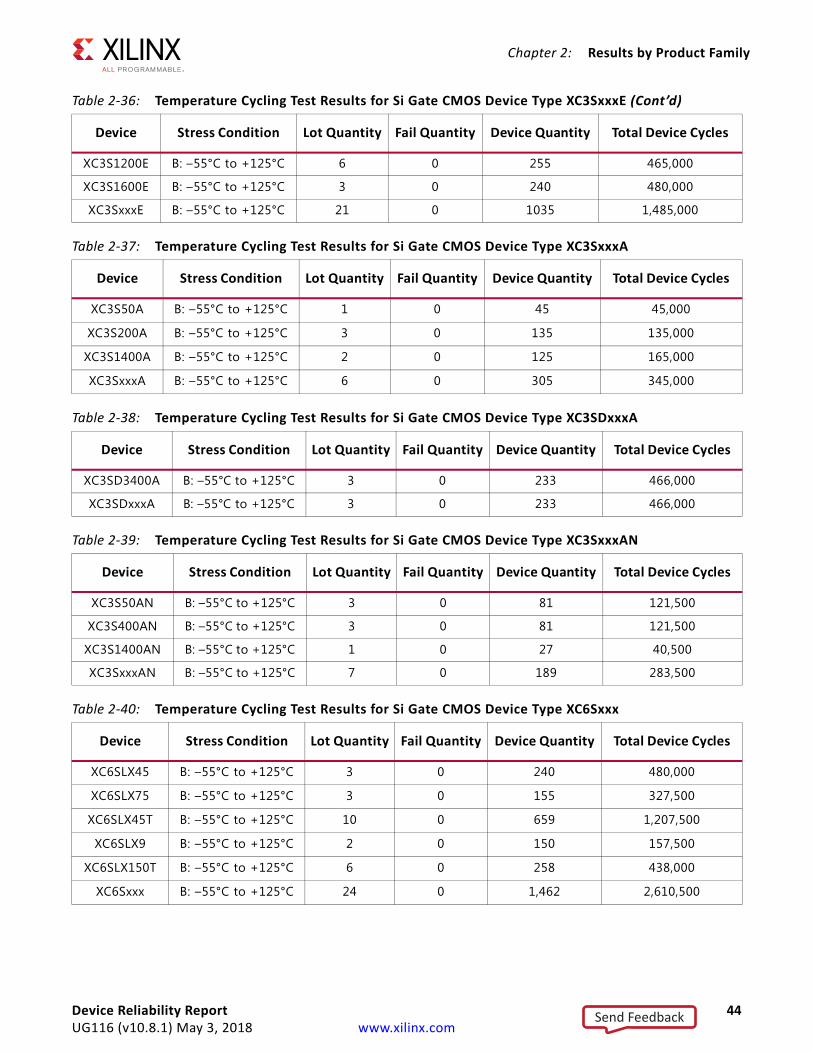
Chapter 2: Results by Product Family
XC3S1200E B: –55°C to +125°C 6 0 255 465,000
XC3S1600E B: –55°C to +125°C 3 0 240 480,000
XC3SxxxE B: –55°C to +125°C 21 0 1035 1,485,000
Table 2-36: Temperature Cycling Test Results for Si Gate CMOS Device Type XC3SxxxE (Cont’d)
Device Stress Condition Lot Quantity Fail Quantity Device Quantity Total Device Cycles
Table 2-37: Temperature Cycling Test Results for Si Gate CMOS Device Type XC3SxxxA
Device Stress Condition Lot Quantity Fail Quantity Device Quantity Total Device Cycles
XC3S50A B: –55°C to +125°C 1 0 45 45,000
XC3S200A B: –55°C to +125°C 3 0 135 135,000
XC3S1400A B: –55°C to +125°C 2 0 125 165,000
XC3SxxxA B: –55°C to +125°C 6 0 305 345,000
Table 2-38: Temperature Cycling Test Results for Si Gate CMOS Device Type XC3SDxxxA
Device Stress Condition Lot Quantity Fail Quantity Device Quantity Total Device Cycles
XC3SD3400A B: –55°C to +125°C 3 0 233 466,000
XC3SDxxxA B: –55°C to +125°C 3 0 233 466,000
Table 2-39: Temperature Cycling Test Results for Si Gate CMOS Device Type XC3SxxxAN
Device Stress Condition Lot Quantity Fail Quantity Device Quantity Total Device Cycles
XC3S50AN B: –55°C to +125°C 3 0 81 121,500
XC3S400AN B: –55°C to +125°C 3 0 81 121,500
XC3S1400AN B: –55°C to +125°C 1 0 27 40,500
XC3SxxxAN B: –55°C to +125°C 7 0 189 283,500
Table 2-40: Temperature Cycling Test Results for Si Gate CMOS Device Type XC6Sxxx
Device Stress Condition Lot Quantity Fail Quantity Device Quantity Total Device Cycles
XC6SLX45 B: –55°C to +125°C 3 0 240 480,000
XC6SLX75 B: –55°C to +125°C 3 0 155 327,500
XC6SLX45T B: –55°C to +125°C 10 0 659 1,207,500
XC6SLX9 B: –55°C to +125°C 2 0 150 157,500
XC6SLX150T B: –55°C to +125°C 6 0 258 438,000
XC6Sxxx B: –55°C to +125°C 24 0 1,462 2,610,500
Device Reliability Report 44UG116 (v10.8.1) May 3, 2018 www.xilinx.com
Send Feedback
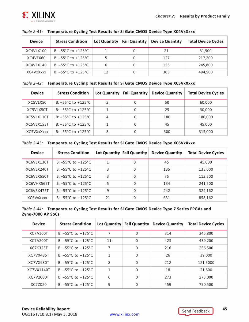
Chapter 2: Results by Product Family
Table 2-41: Temperature Cycling Test Results for Si Gate CMOS Device Type XC4VxXxxx
Device Stress Condition Lot Quantity Fail Quantity Device Quantity Total Device Cycles
XC4VLX100 B: –55°C to +125°C 1 0 21 31,500
XC4VFX60 B: –55°C to +125°C 5 0 127 217,200
XC4VFX140 B: –55°C to +125°C 6 0 155 245,800
XC4VxXxxx B: –55°C to +125°C 12 0 303 494,500
Table 2-42: Temperature Cycling Test Results for Si Gate CMOS Device Type XC5VxXxxx
Device Stress Condition Lot Quantity Fail Quantity Device Quantity Total Device Cycles
XC5VLX50 B: –55°C to +125°C 2 0 50 60,000
XC5VLX50T B: –55°C to +125°C 1 0 25 30,000
XC5VLX110T B: –55°C to +125°C 4 0 180 180,000
XC5VLX155T B: –55°C to +125°C 1 0 45 45,000
XC5VXxXxxx B: –55°C to +125°C 8 0 300 315,000
Table 2-43: Temperature Cycling Test Results for Si Gate CMOS Device Type XC6VxXxxx
Device Stress Condition Lot Quantity Fail Quantity Device Quantity Total Device Cycles
XC6VLX130T B: –55°C to +125°C 1 0 45 45,000
XC6VLX240T B: –55°C to +125°C 3 0 135 135,000
XC6VLX550T B: –55°C to +125°C 3 0 75 112,500
XC6VHX565T B: –55°C to +125°C 5 0 134 241,500
XC6VSX475T B: –55°C to +125°C 9 0 242 324,162
XC6VxXxxx B: –55°C to +125°C 21 0 631 858,162
Table 2-44: Temperature Cycling Test Results for Si Gate CMOS Device Type 7 Series FPGAs and Zynq-7000 AP SoCs
Device Stress Condition Lot Quantity Fail Quantity Device Quantity Total Device Cycles
XC7A100T B: –55°C to +125°C 7 0 314 345,800
XC7A200T B: –55°C to +125°C 11 0 423 439,200
XC7K325T B: –55°C to +125°C 7 0 216 256,500
XC7VX485T B: –55°C to +125°C 1 0 26 39,000
XC7VX980T B: –55°C to +125°C 8 0 212 121,5000
XC7VX1140T B: –55°C to +125°C 1 0 18 21,600
XC7V2000T B: –55°C to +125°C 6 0 273 273,000
XC7Z020 B: –55°C to +125°C 9 0 459 750,500
Device Reliability Report 45UG116 (v10.8.1) May 3, 2018 www.xilinx.com
Send Feedback
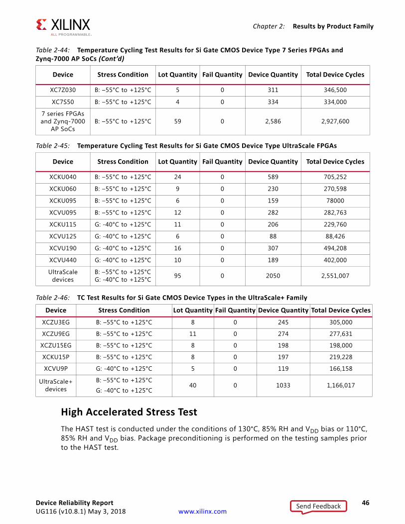
Chapter 2: Results by Product Family
s
High Accelerated Stress TestThe HAST test is conducted under the conditions of 130°C, 85% RH and VDD bias or 110°C, 85% RH and VDD bias. Package preconditioning is performed on the testing samples prior to the HAST test.
XC7Z030 B: –55°C to +125°C 5 0 311 346,500
XC7S50 B: –55°C to +125°C 4 0 334 334,000
7 series FPGAs and Zynq-7000
AP SoCsB: –55°C to +125°C 59 0 2,586 2,927,600
Table 2-45: Temperature Cycling Test Results for Si Gate CMOS Device Type UltraScale FPGAs
Device Stress Condition Lot Quantity Fail Quantity Device Quantity Total Device Cycles
XCKU040 B: –55°C to +125°C 24 0 589 705,252
XCKU060 B: –55°C to +125°C 9 0 230 270,598
XCKU095 B: –55°C to +125°C 6 0 159 78000
XCVU095 B: –55°C to +125°C 12 0 282 282,763
XCKU115 G: -40°C to +125°C 11 0 206 229,760
XCVU125 G: -40°C to +125°C 6 0 88 88,426
XCVU190 G: -40°C to +125°C 16 0 307 494,208
XCVU440 G: -40°C to +125°C 10 0 189 402,000
UltraScale devices
B: –55°C to +125°C G: -40°C to +125°C 95 0 2050 2,551,007
Table 2-44: Temperature Cycling Test Results for Si Gate CMOS Device Type 7 Series FPGAs and Zynq-7000 AP SoCs (Cont’d)
Device Stress Condition Lot Quantity Fail Quantity Device Quantity Total Device Cycles
Table 2-46: TC Test Results for Si Gate CMOS Device Types in the UltraScale+ Family
Device Stress Condition Lot Quantity Fail Quantity Device Quantity Total Device Cycles
XCZU3EG B: –55°C to +125°C 8 0 245 305,000
XCZU9EG B: –55°C to +125°C 11 0 274 277,631
XCZU15EG B: –55°C to +125°C 8 0 198 198,000
XCKU15P B: –55°C to +125°C 8 0 197 219,228
XCVU9P G: -40°C to +125°C 5 0 119 166,158
UltraScale+ devices
B: –55°C to +125°C
G: -40°C to +125°C40 0 1033 1,166,017
Device Reliability Report 46UG116 (v10.8.1) May 3, 2018 www.xilinx.com
Send Feedback
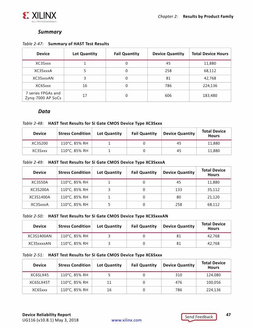
Chapter 2: Results by Product Family
Summary
Data
Table 2-47: Summary of HAST Test Results
Device Lot Quantity Fail Quantity Device Quantity Total Device Hours
XC3Sxxx 1 0 45 11,880
XC3SxxxA 5 0 258 68,112
XC3SxxxAN 3 0 81 42,768
XC6Sxxx 16 0 786 224,136
7 series FPGAs and Zynq-7000 AP SoCs 17 0 606 183,480
Table 2-48: HAST Test Results for Si Gate CMOS Device Type XC3Sxxx
Device Stress Condition Lot Quantity Fail Quantity Device Quantity Total Device Hours
XC3S200 110°C, 85% RH 1 0 45 11,880
XC3Sxxx 110°C, 85% RH 1 0 45 11,880
Table 2-49: HAST Test Results for Si Gate CMOS Device Type XC3SxxxA
Device Stress Condition Lot Quantity Fail Quantity Device Quantity Total Device Hours
XC3S50A 110°C, 85% RH 1 0 45 11,880
XC3S200A 110°C, 85% RH 3 0 133 35,112
XC3S1400A 110°C, 85% RH 1 0 80 21,120
XC3SxxxA 110°C, 85% RH 5 0 258 68,112
Table 2-50: HAST Test Results for Si Gate CMOS Device Type XC3SxxxAN
Device Stress Condition Lot Quantity Fail Quantity Device Quantity Total Device Hours
XC3S1400AN 110°C, 85% RH 3 0 81 42,768
XC3SxxxxAN 110°C, 85% RH 3 0 81 42,768
Table 2-51: HAST Test Results for Si Gate CMOS Device Type XC6Sxxx
Device Stress Condition Lot Quantity Fail Quantity Device Quantity Total Device Hours
XC6SLX45 110°C, 85% RH 5 0 310 124,080
XC6SLX45T 110°C, 85% RH 11 0 476 100,056
XC6Sxxx 110°C, 85% RH 16 0 786 224,136
Device Reliability Report 47UG116 (v10.8.1) May 3, 2018 www.xilinx.com
Send Feedback
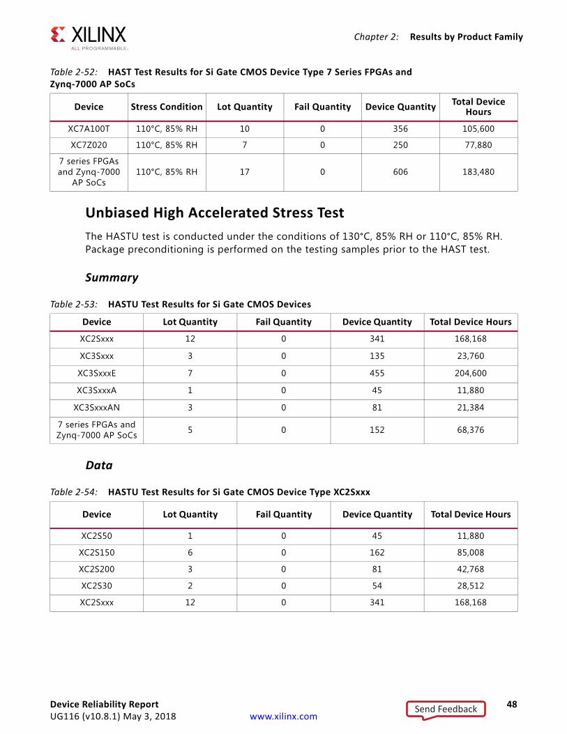
Chapter 2: Results by Product Family
Unbiased High Accelerated Stress TestThe HASTU test is conducted under the conditions of 130°C, 85% RH or 110°C, 85% RH. Package preconditioning is performed on the testing samples prior to the HAST test.
Summary
Data
Table 2-52: HAST Test Results for Si Gate CMOS Device Type 7 Series FPGAs and Zynq-7000 AP SoCs
Device Stress Condition Lot Quantity Fail Quantity Device Quantity Total Device Hours
XC7A100T 110°C, 85% RH 10 0 356 105,600
XC7Z020 110°C, 85% RH 7 0 250 77,880
7 series FPGAs and Zynq-7000
AP SoCs110°C, 85% RH 17 0 606 183,480
Table 2-53: HASTU Test Results for Si Gate CMOS Devices
Device Lot Quantity Fail Quantity Device Quantity Total Device Hours
XC2Sxxx 12 0 341 168,168
XC3Sxxx 3 0 135 23,760
XC3SxxxE 7 0 455 204,600
XC3SxxxA 1 0 45 11,880
XC3SxxxAN 3 0 81 21,384
7 series FPGAs and Zynq-7000 AP SoCs 5 0 152 68,376
Table 2-54: HASTU Test Results for Si Gate CMOS Device Type XC2Sxxx
Device Lot Quantity Fail Quantity Device Quantity Total Device Hours
XC2S50 1 0 45 11,880
XC2S150 6 0 162 85,008
XC2S200 3 0 81 42,768
XC2S30 2 0 54 28,512
XC2Sxxx 12 0 341 168,168
Device Reliability Report 48UG116 (v10.8.1) May 3, 2018 www.xilinx.com
Send Feedback
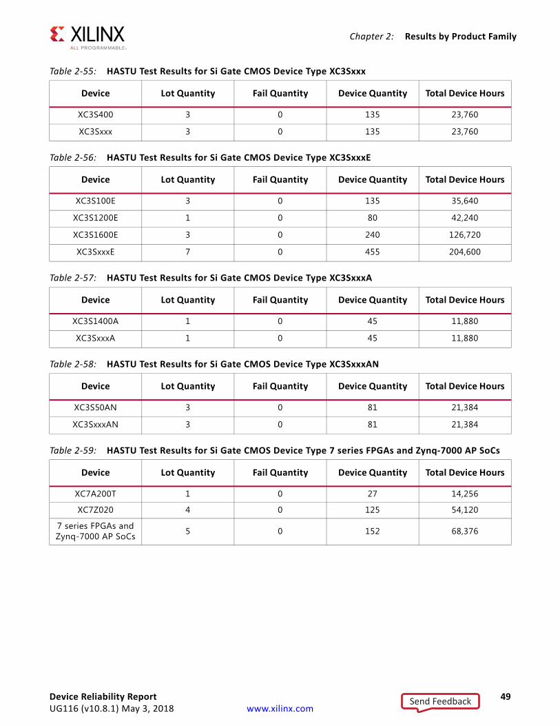
Chapter 2: Results by Product Family
Table 2-55: HASTU Test Results for Si Gate CMOS Device Type XC3Sxxx
Device Lot Quantity Fail Quantity Device Quantity Total Device Hours
XC3S400 3 0 135 23,760
XC3Sxxx 3 0 135 23,760
Table 2-56: HASTU Test Results for Si Gate CMOS Device Type XC3SxxxE
Device Lot Quantity Fail Quantity Device Quantity Total Device Hours
XC3S100E 3 0 135 35,640
XC3S1200E 1 0 80 42,240
XC3S1600E 3 0 240 126,720
XC3SxxxE 7 0 455 204,600
Table 2-57: HASTU Test Results for Si Gate CMOS Device Type XC3SxxxA
Device Lot Quantity Fail Quantity Device Quantity Total Device Hours
XC3S1400A 1 0 45 11,880
XC3SxxxA 1 0 45 11,880
Table 2-58: HASTU Test Results for Si Gate CMOS Device Type XC3SxxxAN
Device Lot Quantity Fail Quantity Device Quantity Total Device Hours
XC3S50AN 3 0 81 21,384
XC3SxxxAN 3 0 81 21,384
Table 2-59: HASTU Test Results for Si Gate CMOS Device Type 7 series FPGAs and Zynq-7000 AP SoCs
Device Lot Quantity Fail Quantity Device Quantity Total Device Hours
XC7A200T 1 0 27 14,256
XC7Z020 4 0 125 54,120
7 series FPGAs and Zynq-7000 AP SoCs 5 0 152 68,376
Device Reliability Report 49UG116 (v10.8.1) May 3, 2018 www.xilinx.com
Send Feedback
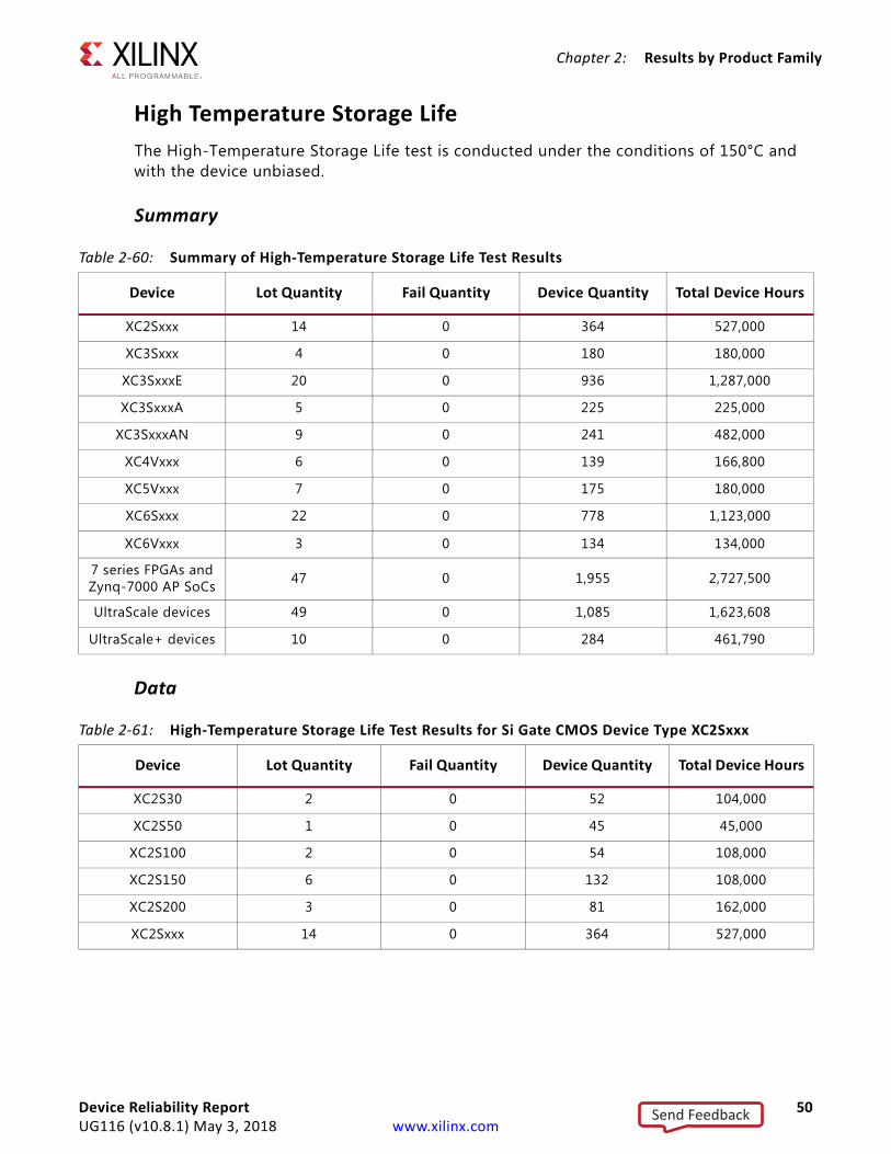
Chapter 2: Results by Product Family
High Temperature Storage LifeThe High-Temperature Storage Life test is conducted under the conditions of 150°C and with the device unbiased.
Summary
Data
Table 2-60: Summary of High-Temperature Storage Life Test Results
Device Lot Quantity Fail Quantity Device Quantity Total Device Hours
XC2Sxxx 14 0 364 527,000
XC3Sxxx 4 0 180 180,000
XC3SxxxE 20 0 936 1,287,000
XC3SxxxA 5 0 225 225,000
XC3SxxxAN 9 0 241 482,000
XC4Vxxx 6 0 139 166,800
XC5Vxxx 7 0 175 180,000
XC6Sxxx 22 0 778 1,123,000
XC6Vxxx 3 0 134 134,000
7 series FPGAs and Zynq-7000 AP SoCs 47 0 1,955 2,727,500
UltraScale devices 49 0 1,085 1,623,608
UltraScale+ devices 10 0 284 461,790
Table 2-61: High-Temperature Storage Life Test Results for Si Gate CMOS Device Type XC2Sxxx
Device Lot Quantity Fail Quantity Device Quantity Total Device Hours
XC2S30 2 0 52 104,000
XC2S50 1 0 45 45,000
XC2S100 2 0 54 108,000
XC2S150 6 0 132 108,000
XC2S200 3 0 81 162,000
XC2Sxxx 14 0 364 527,000
Device Reliability Report 50UG116 (v10.8.1) May 3, 2018 www.xilinx.com
Send Feedback
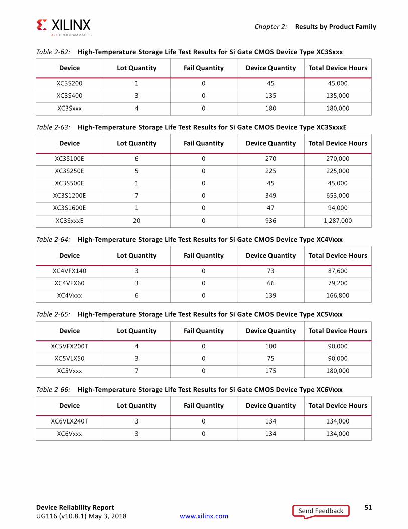
Chapter 2: Results by Product Family
Table 2-62: High-Temperature Storage Life Test Results for Si Gate CMOS Device Type XC3Sxxx
Device Lot Quantity Fail Quantity Device Quantity Total Device Hours
XC3S200 1 0 45 45,000
XC3S400 3 0 135 135,000
XC3Sxxx 4 0 180 180,000
Table 2-63: High-Temperature Storage Life Test Results for Si Gate CMOS Device Type XC3SxxxE
Device Lot Quantity Fail Quantity Device Quantity Total Device Hours
XC3S100E 6 0 270 270,000
XC3S250E 5 0 225 225,000
XC3S500E 1 0 45 45,000
XC3S1200E 7 0 349 653,000
XC3S1600E 1 0 47 94,000
XC3SxxxE 20 0 936 1,287,000
Table 2-64: High-Temperature Storage Life Test Results for Si Gate CMOS Device Type XC4Vxxx
Device Lot Quantity Fail Quantity Device Quantity Total Device Hours
XC4VFX140 3 0 73 87,600
XC4VFX60 3 0 66 79,200
XC4Vxxx 6 0 139 166,800
Table 2-65: High-Temperature Storage Life Test Results for Si Gate CMOS Device Type XC5Vxxx
Device Lot Quantity Fail Quantity Device Quantity Total Device Hours
XC5VFX200T 4 0 100 90,000
XC5VLX50 3 0 75 90,000
XC5Vxxx 7 0 175 180,000
Table 2-66: High-Temperature Storage Life Test Results for Si Gate CMOS Device Type XC6Vxxx
Device Lot Quantity Fail Quantity Device Quantity Total Device Hours
XC6VLX240T 3 0 134 134,000
XC6Vxxx 3 0 134 134,000
Device Reliability Report 51UG116 (v10.8.1) May 3, 2018 www.xilinx.com
Send Feedback
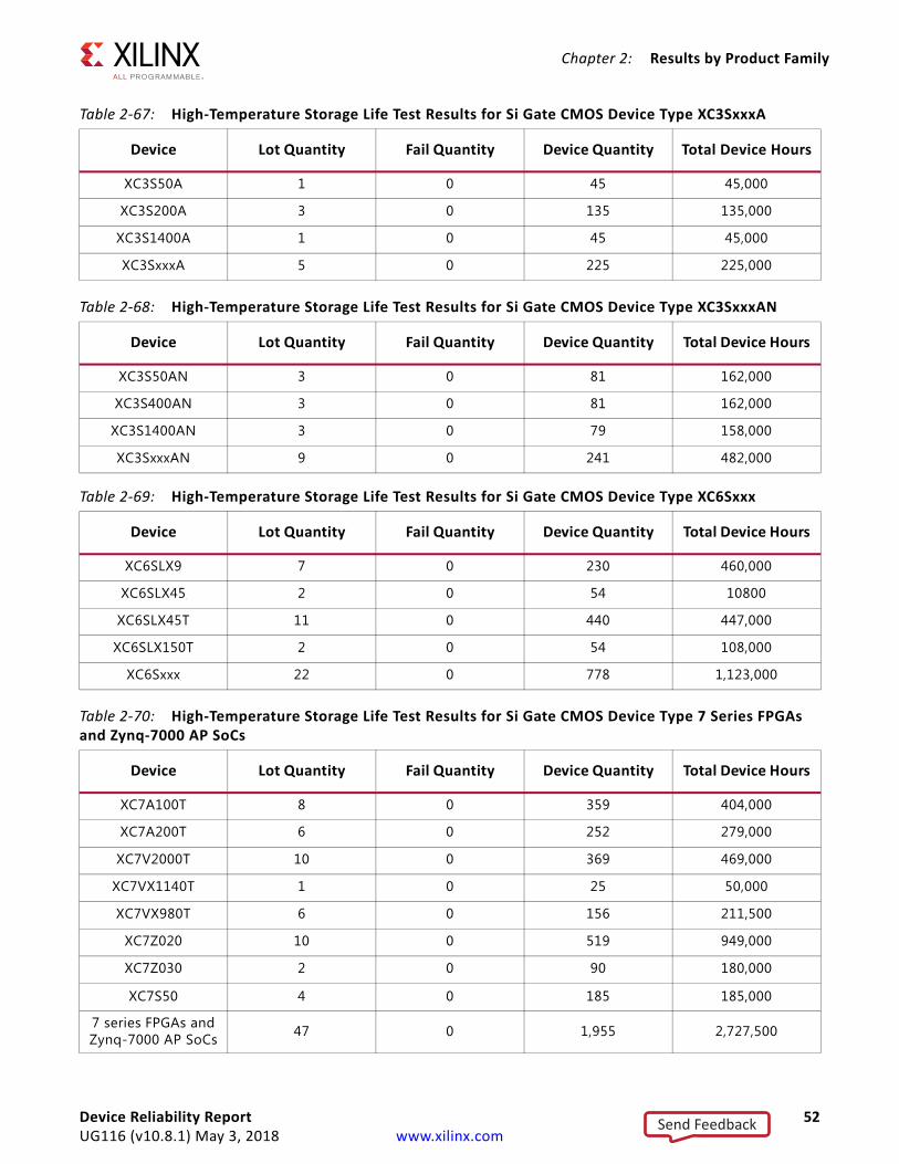
Chapter 2: Results by Product Family
Table 2-67: High-Temperature Storage Life Test Results for Si Gate CMOS Device Type XC3SxxxA
Device Lot Quantity Fail Quantity Device Quantity Total Device Hours
XC3S50A 1 0 45 45,000
XC3S200A 3 0 135 135,000
XC3S1400A 1 0 45 45,000
XC3SxxxA 5 0 225 225,000
Table 2-68: High-Temperature Storage Life Test Results for Si Gate CMOS Device Type XC3SxxxAN
Device Lot Quantity Fail Quantity Device Quantity Total Device Hours
XC3S50AN 3 0 81 162,000
XC3S400AN 3 0 81 162,000
XC3S1400AN 3 0 79 158,000
XC3SxxxAN 9 0 241 482,000
Table 2-69: High-Temperature Storage Life Test Results for Si Gate CMOS Device Type XC6Sxxx
Device Lot Quantity Fail Quantity Device Quantity Total Device Hours
XC6SLX9 7 0 230 460,000
XC6SLX45 2 0 54 10800
XC6SLX45T 11 0 440 447,000
XC6SLX150T 2 0 54 108,000
XC6Sxxx 22 0 778 1,123,000
Table 2-70: High-Temperature Storage Life Test Results for Si Gate CMOS Device Type 7 Series FPGAs and Zynq-7000 AP SoCs
Device Lot Quantity Fail Quantity Device Quantity Total Device Hours
XC7A100T 8 0 359 404,000
XC7A200T 6 0 252 279,000
XC7V2000T 10 0 369 469,000
XC7VX1140T 1 0 25 50,000
XC7VX980T 6 0 156 211,500
XC7Z020 10 0 519 949,000
XC7Z030 2 0 90 180,000
XC7S50 4 0 185 185,000
7 series FPGAs and Zynq-7000 AP SoCs 47 0 1,955 2,727,500
Device Reliability Report 52UG116 (v10.8.1) May 3, 2018 www.xilinx.com
Send Feedback
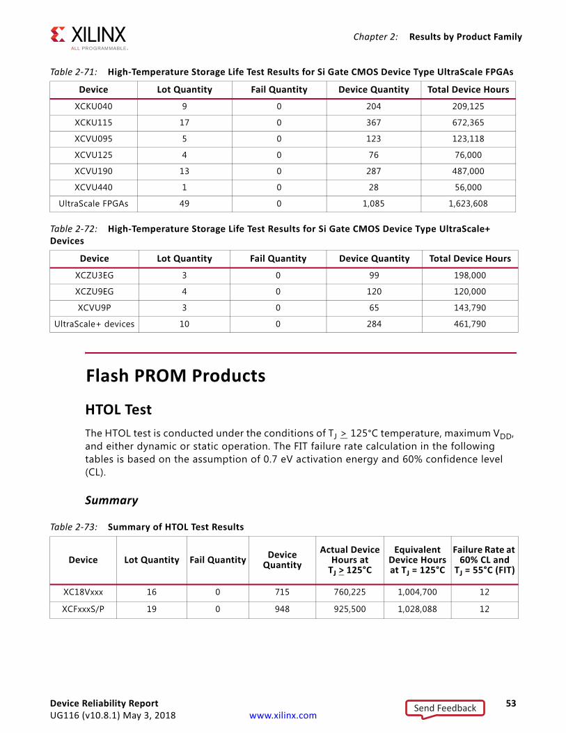
Chapter 2: Results by Product Family
Flash PROM Products
HTOL TestThe HTOL test is conducted under the conditions of TJ > 125°C temperature, maximum VDD, and either dynamic or static operation. The FIT failure rate calculation in the following tables is based on the assumption of 0.7 eV activation energy and 60% confidence level (CL).
Summary
Table 2-71: High-Temperature Storage Life Test Results for Si Gate CMOS Device Type UltraScale FPGAs
Device Lot Quantity Fail Quantity Device Quantity Total Device Hours
XCKU040 9 0 204 209,125
XCKU115 17 0 367 672,365
XCVU095 5 0 123 123,118
XCVU125 4 0 76 76,000
XCVU190 13 0 287 487,000
XCVU440 1 0 28 56,000
UltraScale FPGAs 49 0 1,085 1,623,608
Table 2-72: High-Temperature Storage Life Test Results for Si Gate CMOS Device Type UltraScale+ Devices
Device Lot Quantity Fail Quantity Device Quantity Total Device Hours
XCZU3EG 3 0 99 198,000
XCZU9EG 4 0 120 120,000
XCVU9P 3 0 65 143,790
UltraScale+ devices 10 0 284 461,790
Table 2-73: Summary of HTOL Test Results
Device Lot Quantity Fail Quantity Device Quantity
Actual Device Hours at
TJ > 125°C
Equivalent Device Hours at TJ = 125°C
Failure Rate at 60% CL and
TJ = 55°C (FIT)
XC18Vxxx 16 0 715 760,225 1,004,700 12
XCFxxxS/P 19 0 948 925,500 1,028,088 12
Device Reliability Report 53UG116 (v10.8.1) May 3, 2018 www.xilinx.com
Send Feedback
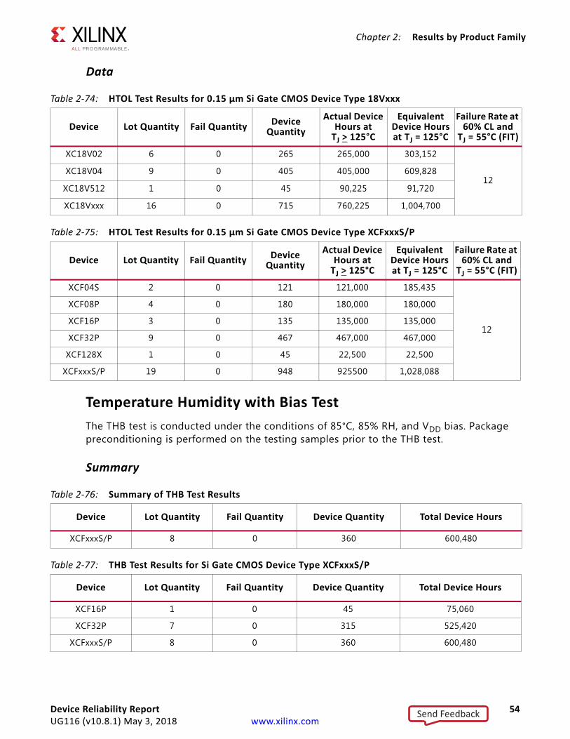
Chapter 2: Results by Product Family
Data
Temperature Humidity with Bias TestThe THB test is conducted under the conditions of 85°C, 85% RH, and VDD bias. Package preconditioning is performed on the testing samples prior to the THB test.
Summary
Table 2-74: HTOL Test Results for 0.15 µm Si Gate CMOS Device Type 18Vxxx
Device Lot Quantity Fail Quantity Device Quantity
Actual Device Hours at
TJ > 125°C
Equivalent Device Hours at TJ = 125°C
Failure Rate at 60% CL and
TJ = 55°C (FIT)
XC18V02 6 0 265 265,000 303,152
12XC18V04 9 0 405 405,000 609,828
XC18V512 1 0 45 90,225 91,720
XC18Vxxx 16 0 715 760,225 1,004,700
Table 2-75: HTOL Test Results for 0.15 µm Si Gate CMOS Device Type XCFxxxS/P
Device Lot Quantity Fail Quantity Device Quantity
Actual Device Hours at
TJ > 125°C
Equivalent Device Hours at TJ = 125°C
Failure Rate at 60% CL and
TJ = 55°C (FIT)
XCF04S 2 0 121 121,000 185,435
12
XCF08P 4 0 180 180,000 180,000
XCF16P 3 0 135 135,000 135,000
XCF32P 9 0 467 467,000 467,000
XCF128X 1 0 45 22,500 22,500
XCFxxxS/P 19 0 948 925500 1,028,088
Table 2-76: Summary of THB Test Results
Device Lot Quantity Fail Quantity Device Quantity Total Device Hours
XCFxxxS/P 8 0 360 600,480
Table 2-77: THB Test Results for Si Gate CMOS Device Type XCFxxxS/P
Device Lot Quantity Fail Quantity Device Quantity Total Device Hours
XCF16P 1 0 45 75,060
XCF32P 7 0 315 525,420
XCFxxxS/P 8 0 360 600,480
Device Reliability Report 54UG116 (v10.8.1) May 3, 2018 www.xilinx.com
Send Feedback
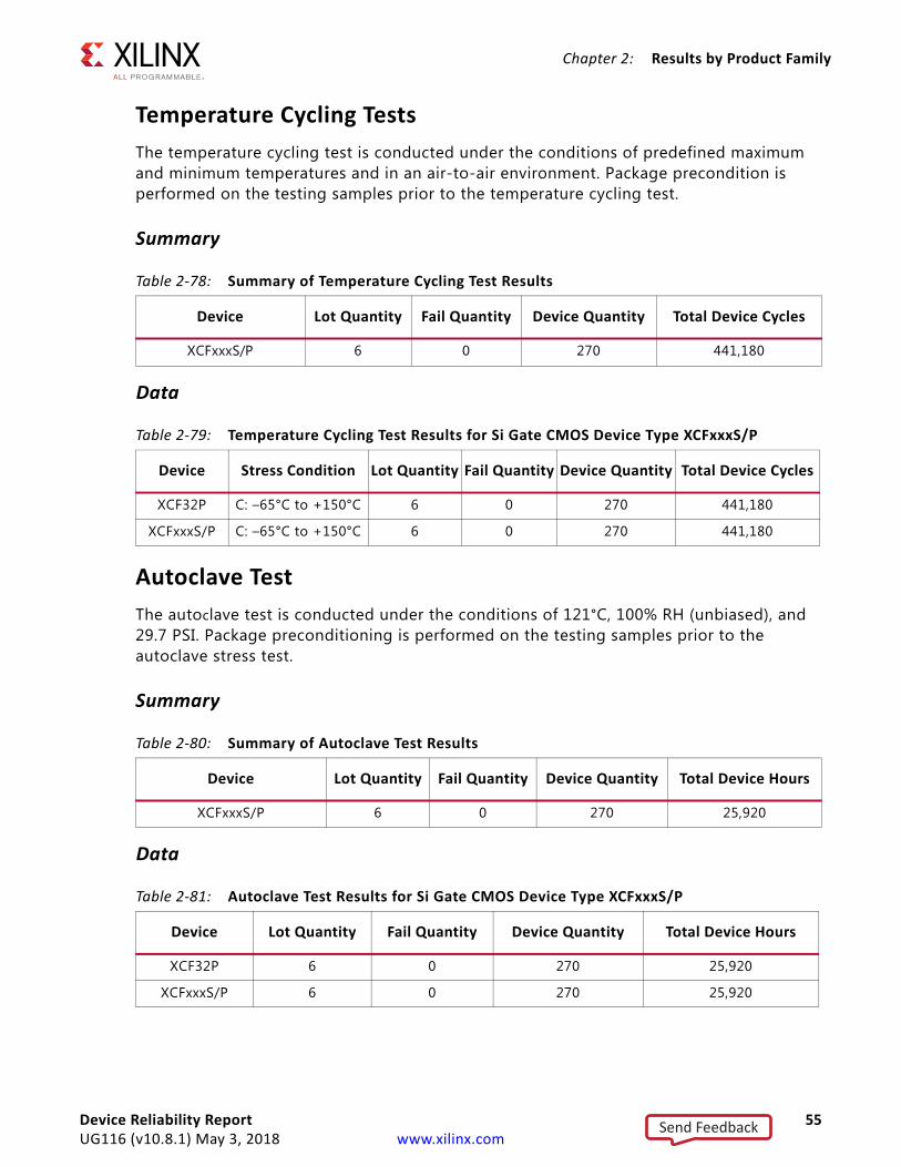
Chapter 2: Results by Product Family
Temperature Cycling TestsThe temperature cycling test is conducted under the conditions of predefined maximum and minimum temperatures and in an air-to-air environment. Package precondition is performed on the testing samples prior to the temperature cycling test.
Summary
Data
Autoclave TestThe autoclave test is conducted under the conditions of 121°C, 100% RH (unbiased), and 29.7 PSI. Package preconditioning is performed on the testing samples prior to the autoclave stress test.
Summary
Data
Table 2-78: Summary of Temperature Cycling Test Results
Device Lot Quantity Fail Quantity Device Quantity Total Device Cycles
XCFxxxS/P 6 0 270 441,180
Table 2-79: Temperature Cycling Test Results for Si Gate CMOS Device Type XCFxxxS/P
Device Stress Condition Lot Quantity Fail Quantity Device Quantity Total Device Cycles
XCF32P C: –65°C to +150°C 6 0 270 441,180
XCFxxxS/P C: –65°C to +150°C 6 0 270 441,180
Table 2-80: Summary of Autoclave Test Results
Device Lot Quantity Fail Quantity Device Quantity Total Device Hours
XCFxxxS/P 6 0 270 25,920
Table 2-81: Autoclave Test Results for Si Gate CMOS Device Type XCFxxxS/P
Device Lot Quantity Fail Quantity Device Quantity Total Device Hours
XCF32P 6 0 270 25,920
XCFxxxS/P 6 0 270 25,920
Device Reliability Report 55UG116 (v10.8.1) May 3, 2018 www.xilinx.com
Send Feedback
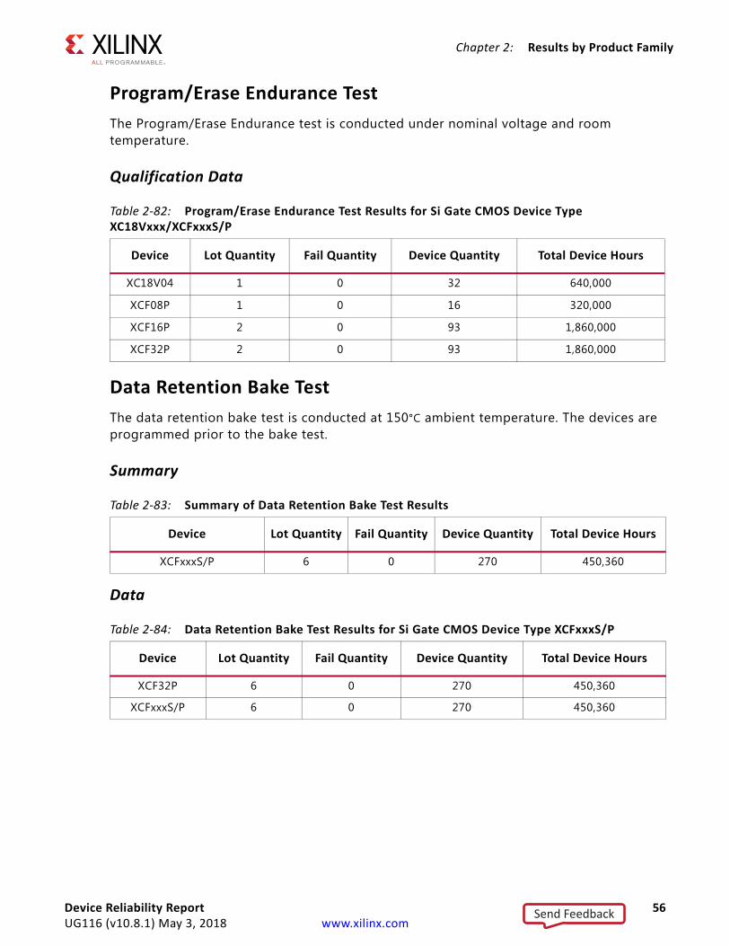
Chapter 2: Results by Product Family
Program/Erase Endurance TestThe Program/Erase Endurance test is conducted under nominal voltage and room temperature.
Qualification Data
Data Retention Bake TestThe data retention bake test is conducted at 150°C ambient temperature. The devices are programmed prior to the bake test.
Summary
Data
Table 2-82: Program/Erase Endurance Test Results for Si Gate CMOS Device Type XC18Vxxx/XCFxxxS/P
Device Lot Quantity Fail Quantity Device Quantity Total Device Hours
XC18V04 1 0 32 640,000
XCF08P 1 0 16 320,000
XCF16P 2 0 93 1,860,000
XCF32P 2 0 93 1,860,000
Table 2-83: Summary of Data Retention Bake Test Results
Device Lot Quantity Fail Quantity Device Quantity Total Device Hours
XCFxxxS/P 6 0 270 450,360
Table 2-84: Data Retention Bake Test Results for Si Gate CMOS Device Type XCFxxxS/P
Device Lot Quantity Fail Quantity Device Quantity Total Device Hours
XCF32P 6 0 270 450,360
XCFxxxS/P 6 0 270 450,360
Device Reliability Report 56UG116 (v10.8.1) May 3, 2018 www.xilinx.com
Send Feedback
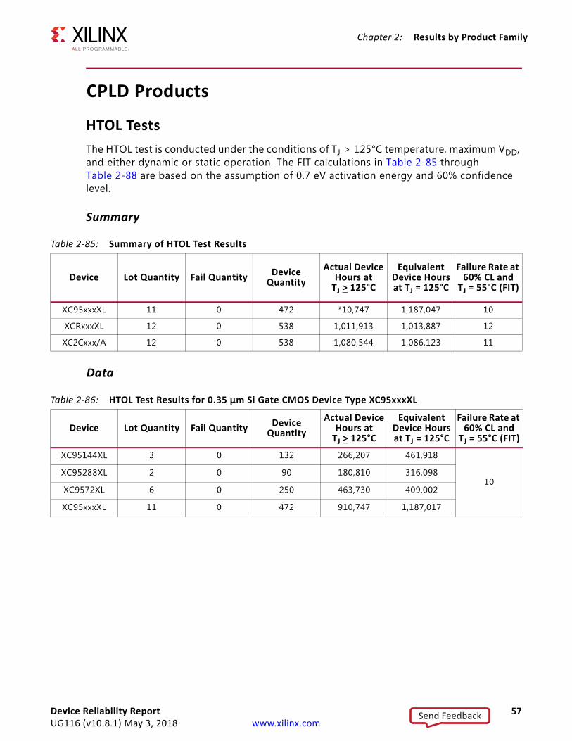
Chapter 2: Results by Product Family
CPLD Products
HTOL TestsThe HTOL test is conducted under the conditions of TJ > 125°C temperature, maximum VDD, and either dynamic or static operation. The FIT calculations in Table 2-85 through Table 2-88 are based on the assumption of 0.7 eV activation energy and 60% confidence level.
Summary
Data
Table 2-85: Summary of HTOL Test Results
Device Lot Quantity Fail Quantity Device Quantity
Actual Device Hours at
TJ > 125°C
Equivalent Device Hours at TJ = 125°C
Failure Rate at 60% CL and
TJ = 55°C (FIT)
XC95xxxXL 11 0 472 *10,747 1,187,047 10
XCRxxxXL 12 0 538 1,011,913 1,013,887 12
XC2Cxxx/A 12 0 538 1,080,544 1,086,123 11
Table 2-86: HTOL Test Results for 0.35 µm Si Gate CMOS Device Type XC95xxxXL
Device Lot Quantity Fail Quantity Device Quantity
Actual Device Hours at
TJ > 125°C
Equivalent Device Hours at TJ = 125°C
Failure Rate at 60% CL and
TJ = 55°C (FIT)
XC95144XL 3 0 132 266,207 461,918
10XC95288XL 2 0 90 180,810 316,098
XC9572XL 6 0 250 463,730 409,002
XC95xxxXL 11 0 472 910,747 1,187,017
Device Reliability Report 57UG116 (v10.8.1) May 3, 2018 www.xilinx.com
Send Feedback
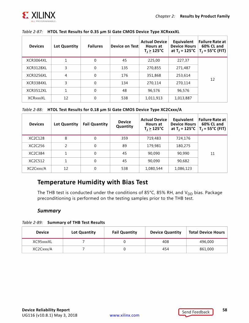
Chapter 2: Results by Product Family
Temperature Humidity with Bias TestThe THB test is conducted under the conditions of 85°C, 85% RH, and VDD bias. Package preconditioning is performed on the testing samples prior to the THB test.
Summary
Table 2-87: HTOL Test Results for 0.35 µm Si Gate CMOS Device Type XCRxxxXL
Devices Lot Quantity Failures Device on TestActual Device
Hours at TJ > 125°C
Equivalent Device Hours at TJ = 125°C
Failure Rate at 60% CL and
TJ = 55°C (FIT)
XCR3064XL 1 0 45 225,00 227,37
12
XCR3128XL 3 0 135 270,855 271,487
XCR3256XL 4 0 176 351,868 253,614
XCR3384XL 3 0 134 270,114 270,114
XCR3512XL 1 0 48 96,576 96,576
XCRxxxXL 12 0 538 1,011,913 1,013,887
Table 2-88: HTOL Test Results for 0.18 µm Si Gate CMOS Device Type XC2Cxxx/A
Devices Lot Quantity Fail Quantity Device Quantity
Actual Device Hours at
TJ > 125°C
Equivalent Device Hours at TJ = 125°C
Failure Rate at 60% CL and
TJ = 55°C (FIT)
XC2C128 8 0 359 719,483 724,176
11
XC2C256 2 0 89 179,981 180,275
XC2C384 1 0 45 90,090 90,990
XC2C512 1 0 45 90,090 90,682
XC2Cxxx/A 12 0 538 1,080,544 1,086,123
Table 2-89: Summary of THB Test Results
Device Lot Quantity Fail Quantity Device Quantity Total Device Hours
XC95xxxXL 7 0 408 496,000
XC2Cxxx/A 7 0 454 861,000
Device Reliability Report 58UG116 (v10.8.1) May 3, 2018 www.xilinx.com
Send Feedback
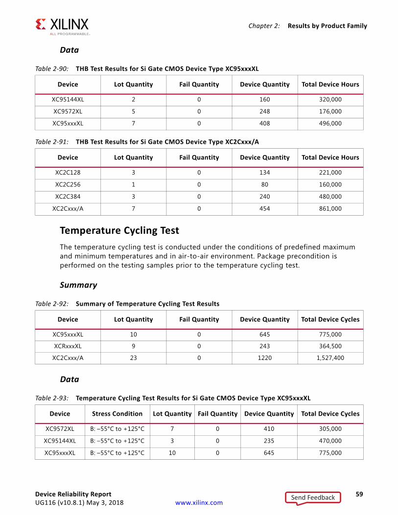
Chapter 2: Results by Product Family
Data
Temperature Cycling TestThe temperature cycling test is conducted under the conditions of predefined maximum and minimum temperatures and in air-to-air environment. Package precondition is performed on the testing samples prior to the temperature cycling test.
Summary
Data
Table 2-90: THB Test Results for Si Gate CMOS Device Type XC95xxxXL
Device Lot Quantity Fail Quantity Device Quantity Total Device Hours
XC95144XL 2 0 160 320,000
XC9572XL 5 0 248 176,000
XC95xxxXL 7 0 408 496,000
Table 2-91: THB Test Results for Si Gate CMOS Device Type XC2Cxxx/A
Device Lot Quantity Fail Quantity Device Quantity Total Device Hours
XC2C128 3 0 134 221,000
XC2C256 1 0 80 160,000
XC2C384 3 0 240 480,000
XC2Cxxx/A 7 0 454 861,000
Table 2-92: Summary of Temperature Cycling Test Results
Device Lot Quantity Fail Quantity Device Quantity Total Device Cycles
XC95xxxXL 10 0 645 775,000
XCRxxxXL 9 0 243 364,500
XC2Cxxx/A 23 0 1220 1,527,400
Table 2-93: Temperature Cycling Test Results for Si Gate CMOS Device Type XC95xxxXL
Device Stress Condition Lot Quantity Fail Quantity Device Quantity Total Device Cycles
XC9572XL B: –55°C to +125°C 7 0 410 305,000
XC95144XL B: –55°C to +125°C 3 0 235 470,000
XC95xxxXL B: –55°C to +125°C 10 0 645 775,000
Device Reliability Report 59UG116 (v10.8.1) May 3, 2018 www.xilinx.com
Send Feedback
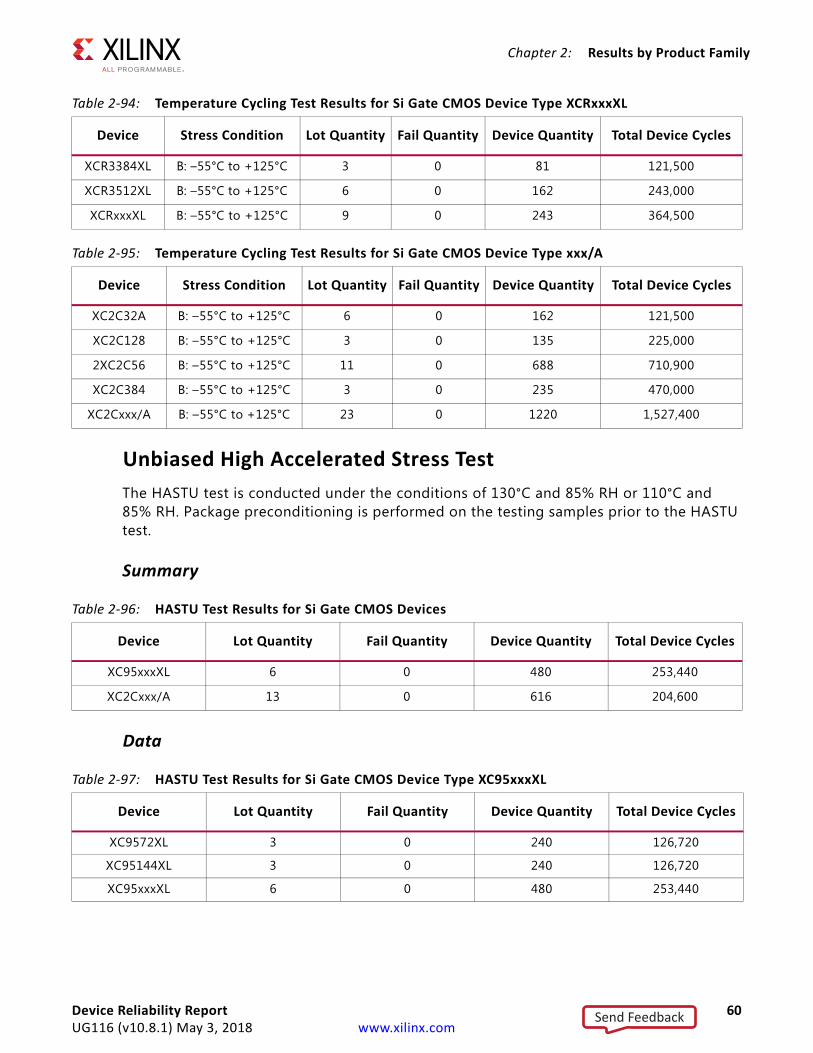
Chapter 2: Results by Product Family
Unbiased High Accelerated Stress TestThe HASTU test is conducted under the conditions of 130°C and 85% RH or 110°C and 85% RH. Package preconditioning is performed on the testing samples prior to the HASTU test.
Summary
Data
Table 2-94: Temperature Cycling Test Results for Si Gate CMOS Device Type XCRxxxXL
Device Stress Condition Lot Quantity Fail Quantity Device Quantity Total Device Cycles
XCR3384XL B: –55°C to +125°C 3 0 81 121,500
XCR3512XL B: –55°C to +125°C 6 0 162 243,000
XCRxxxXL B: –55°C to +125°C 9 0 243 364,500
Table 2-95: Temperature Cycling Test Results for Si Gate CMOS Device Type xxx/A
Device Stress Condition Lot Quantity Fail Quantity Device Quantity Total Device Cycles
XC2C32A B: –55°C to +125°C 6 0 162 121,500
XC2C128 B: –55°C to +125°C 3 0 135 225,000
2XC2C56 B: –55°C to +125°C 11 0 688 710,900
XC2C384 B: –55°C to +125°C 3 0 235 470,000
XC2Cxxx/A B: –55°C to +125°C 23 0 1220 1,527,400
Table 2-96: HASTU Test Results for Si Gate CMOS Devices
Device Lot Quantity Fail Quantity Device Quantity Total Device Cycles
XC95xxxXL 6 0 480 253,440
XC2Cxxx/A 13 0 616 204,600
Table 2-97: HASTU Test Results for Si Gate CMOS Device Type XC95xxxXL
Device Lot Quantity Fail Quantity Device Quantity Total Device Cycles
XC9572XL 3 0 240 126,720
XC95144XL 3 0 240 126,720
XC95xxxXL 6 0 480 253,440
Device Reliability Report 60UG116 (v10.8.1) May 3, 2018 www.xilinx.com
Send Feedback
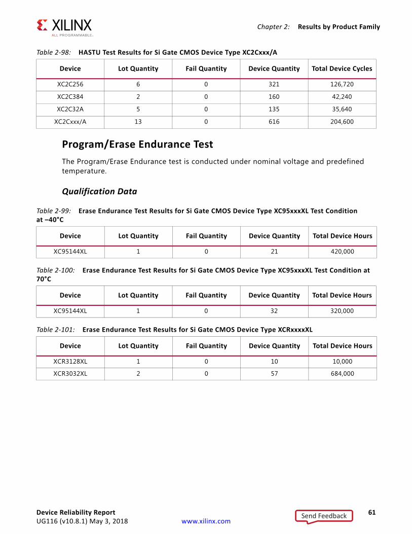
Chapter 2: Results by Product Family
Program/Erase Endurance TestThe Program/Erase Endurance test is conducted under nominal voltage and predefined temperature.
Qualification Data
Table 2-98: HASTU Test Results for Si Gate CMOS Device Type XC2Cxxx/A
Device Lot Quantity Fail Quantity Device Quantity Total Device Cycles
XC2C256 6 0 321 126,720
XC2C384 2 0 160 42,240
XC2C32A 5 0 135 35,640
XC2Cxxx/A 13 0 616 204,600
Table 2-99: Erase Endurance Test Results for Si Gate CMOS Device Type XC95xxxXL Test Conditionat –40°C
Device Lot Quantity Fail Quantity Device Quantity Total Device Hours
XC95144XL 1 0 21 420,000
Table 2-100: Erase Endurance Test Results for Si Gate CMOS Device Type XC95xxxXL Test Condition at 70°C
Device Lot Quantity Fail Quantity Device Quantity Total Device Hours
XC95144XL 1 0 32 320,000
Table 2-101: Erase Endurance Test Results for Si Gate CMOS Device Type XCRxxxxXL
Device Lot Quantity Fail Quantity Device Quantity Total Device Hours
XCR3128XL 1 0 10 10,000
XCR3032XL 2 0 57 684,000
Device Reliability Report 61UG116 (v10.8.1) May 3, 2018 www.xilinx.com
Send Feedback
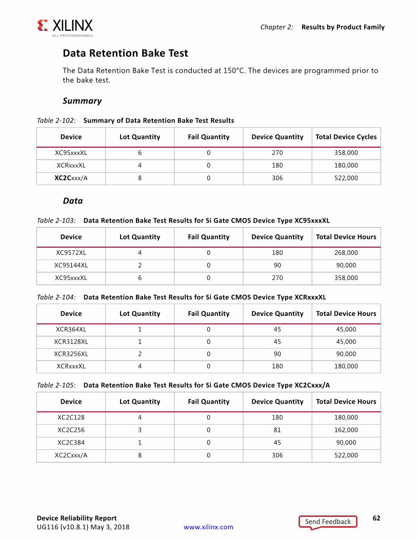
Chapter 2: Results by Product Family
Data Retention Bake TestThe Data Retention Bake Test is conducted at 150°C. The devices are programmed prior to the bake test.
Summary
Data
Table 2-102: Summary of Data Retention Bake Test Results
Device Lot Quantity Fail Quantity Device Quantity Total Device Cycles
XC95xxxXL 6 0 270 358,000
XCRxxxXL 4 0 180 180,000
XC2Cxxx/A 8 0 306 522,000
Table 2-103: Data Retention Bake Test Results for Si Gate CMOS Device Type XC95xxxXL
Device Lot Quantity Fail Quantity Device Quantity Total Device Hours
XC9572XL 4 0 180 268,000
XC95144XL 2 0 90 90,000
XC95xxxXL 6 0 270 358,000
Table 2-104: Data Retention Bake Test Results for Si Gate CMOS Device Type XCRxxxXL
Device Lot Quantity Fail Quantity Device Quantity Total Device Hours
XCR364XL 1 0 45 45,000
XCR3128XL 1 0 45 45,000
XCR3256XL 2 0 90 90,000
XCRxxxXL 4 0 180 180,000
Table 2-105: Data Retention Bake Test Results for Si Gate CMOS Device Type XC2Cxxx/A
Device Lot Quantity Fail Quantity Device Quantity Total Device Hours
XC2C128 4 0 180 180,000
XC2C256 3 0 81 162,000
XC2C384 1 0 45 90,000
XC2Cxxx/A 8 0 306 522,000
Device Reliability Report 62UG116 (v10.8.1) May 3, 2018 www.xilinx.com
Send Feedback
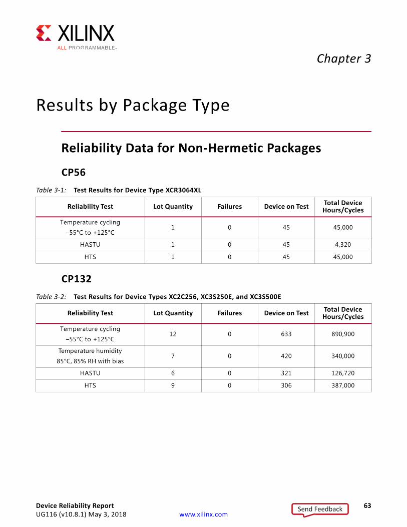
Chapter 3
Results by Package Type
Reliability Data for Non-Hermetic Packages
CP56
CP132
Table 3-1: Test Results for Device Type XCR3064XL
Reliability Test Lot Quantity Failures Device on Test Total Device Hours/Cycles
Temperature cycling
–55°C to +125°C1 0 45 45,000
HASTU 1 0 45 4,320
HTS 1 0 45 45,000
Table 3-2: Test Results for Device Types XC2C256, XC3S250E, and XC3S500E
Reliability Test Lot Quantity Failures Device on Test Total Device Hours/Cycles
Temperature cycling
–55°C to +125°C12 0 633 890,900
Temperature humidity
85°C, 85% RH with bias7 0 420 340,000
HASTU 6 0 321 126,720
HTS 9 0 306 387,000
Device Reliability Report 63UG116 (v10.8.1) May 3, 2018 www.xilinx.com
Send Feedback
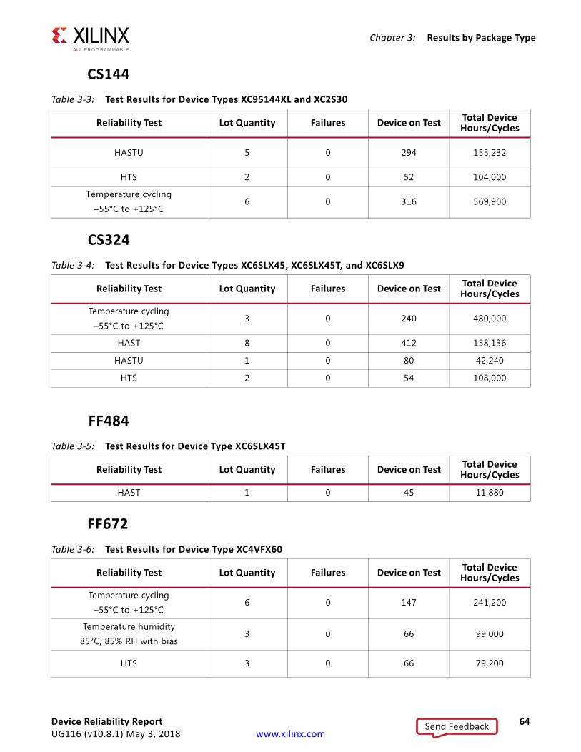
Chapter 3: Results by Package Type
CS144
CS324
FF484
FF672
Table 3-3: Test Results for Device Types XC95144XL and XC2S30
Reliability Test Lot Quantity Failures Device on Test Total Device Hours/Cycles
HASTU 5 0 294 155,232
HTS 2 0 52 104,000
Temperature cycling
–55°C to +125°C6 0 316 569,900
Table 3-4: Test Results for Device Types XC6SLX45, XC6SLX45T, and XC6SLX9
Reliability Test Lot Quantity Failures Device on Test Total Device Hours/Cycles
Temperature cycling
–55°C to +125°C3 0 240 480,000
HAST 8 0 412 158,136
HASTU 1 0 80 42,240
HTS 2 0 54 108,000
Table 3-5: Test Results for Device Type XC6SLX45T
Reliability Test Lot Quantity Failures Device on Test Total Device Hours/Cycles
HAST 1 0 45 11,880
Table 3-6: Test Results for Device Type XC4VFX60
Reliability Test Lot Quantity Failures Device on Test Total Device Hours/Cycles
Temperature cycling
–55°C to +125°C6 0 147 241,200
Temperature humidity
85°C, 85% RH with bias3 0 66 99,000
HTS 3 0 66 79,200
Device Reliability Report 64UG116 (v10.8.1) May 3, 2018 www.xilinx.com
Send Feedback
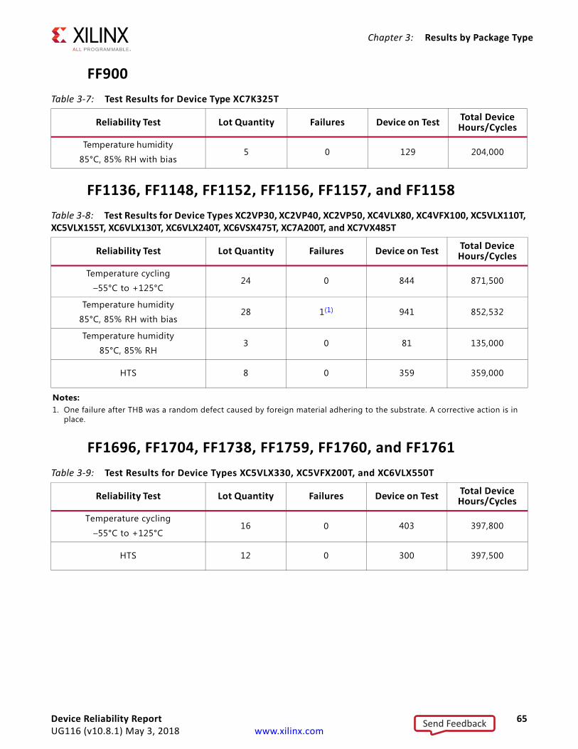
Chapter 3: Results by Package Type
FF900
FF1136, FF1148, FF1152, FF1156, FF1157, and FF1158
FF1696, FF1704, FF1738, FF1759, FF1760, and FF1761
Table 3-7: Test Results for Device Type XC7K325T
Reliability Test Lot Quantity Failures Device on Test Total Device Hours/Cycles
Temperature humidity
85°C, 85% RH with bias5 0 129 204,000
Table 3-8: Test Results for Device Types XC2VP30, XC2VP40, XC2VP50, XC4VLX80, XC4VFX100, XC5VLX110T, XC5VLX155T, XC6VLX130T, XC6VLX240T, XC6VSX475T, XC7A200T, and XC7VX485T
Reliability Test Lot Quantity Failures Device on Test Total Device Hours/Cycles
Temperature cycling
–55°C to +125°C24 0 844 871,500
Temperature humidity
85°C, 85% RH with bias28 1(1) 941 852,532
Temperature humidity
85°C, 85% RH3 0 81 135,000
HTS 8 0 359 359,000
Notes: 1. One failure after THB was a random defect caused by foreign material adhering to the substrate. A corrective action is in
place.
Table 3-9: Test Results for Device Types XC5VLX330, XC5VFX200T, and XC6VLX550T
Reliability Test Lot Quantity Failures Device on Test Total Device Hours/Cycles
Temperature cycling
–55°C to +125°C16 0 403 397,800
HTS 12 0 300 397,500
Device Reliability Report 65UG116 (v10.8.1) May 3, 2018 www.xilinx.com
Send Feedback
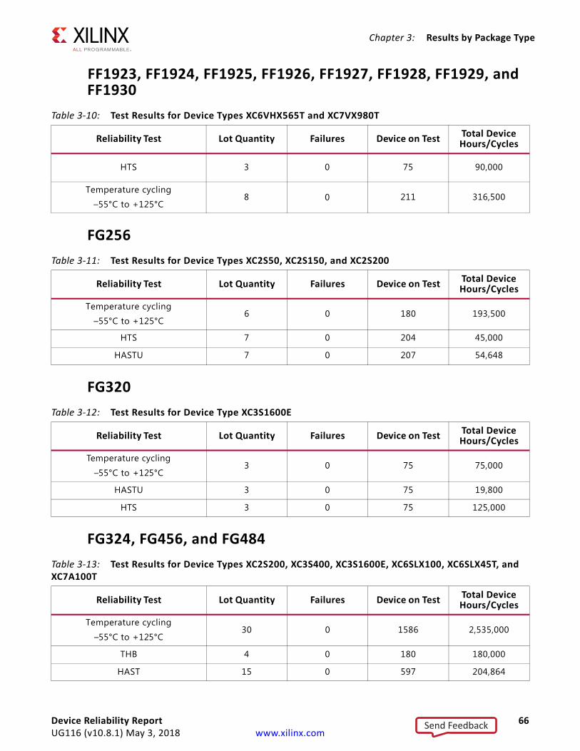
Chapter 3: Results by Package Type
FF1923, FF1924, FF1925, FF1926, FF1927, FF1928, FF1929, and FF1930
FG256
FG320
FG324, FG456, and FG484
Table 3-10: Test Results for Device Types XC6VHX565T and XC7VX980T
Reliability Test Lot Quantity Failures Device on Test Total Device Hours/Cycles
HTS 3 0 75 90,000
Temperature cycling
–55°C to +125°C8 0 211 316,500
Table 3-11: Test Results for Device Types XC2S50, XC2S150, and XC2S200
Reliability Test Lot Quantity Failures Device on Test Total Device Hours/Cycles
Temperature cycling
–55°C to +125°C6 0 180 193,500
HTS 7 0 204 45,000
HASTU 7 0 207 54,648
Table 3-12: Test Results for Device Type XC3S1600E
Reliability Test Lot Quantity Failures Device on Test Total Device Hours/Cycles
Temperature cycling
–55°C to +125°C3 0 75 75,000
HASTU 3 0 75 19,800
HTS 3 0 75 125,000
Table 3-13: Test Results for Device Types XC2S200, XC3S400, XC3S1600E, XC6SLX100, XC6SLX45T, and XC7A100T
Reliability Test Lot Quantity Failures Device on Test Total Device Hours/Cycles
Temperature cycling
–55°C to +125°C30 0 1586 2,535,000
THB 4 0 180 180,000
HAST 15 0 597 204,864
Device Reliability Report 66UG116 (v10.8.1) May 3, 2018 www.xilinx.com
Send Feedback
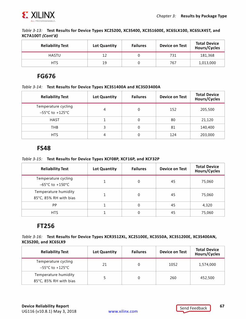
Chapter 3: Results by Package Type
FG676
FS48
FT256
HASTU 12 0 731 181,368
HTS 19 0 767 1,013,000
Table 3-13: Test Results for Device Types XC2S200, XC3S400, XC3S1600E, XC6SLX100, XC6SLX45T, and XC7A100T (Cont’d)
Reliability Test Lot Quantity Failures Device on Test Total Device Hours/Cycles
Table 3-14: Test Results for Device Types XC3S1400A and XC3SD3400A
Reliability Test Lot Quantity Failures Device on Test Total Device Hours/Cycles
Temperature cycling
–55°C to +125°C4 0 152 205,500
HAST 1 0 80 21,120
THB 3 0 81 140,400
HTS 4 0 124 203,000
Table 3-15: Test Results for Device Types XCF08P, XCF16P, and XCF32P
Reliability Test Lot Quantity Failures Device on Test Total Device Hours/Cycles
Temperature cycling
–65°C to +150°C1 0 45 75,060
Temperature humidity
85°C, 85% RH with bias1 0 45 75,060
PP 1 0 45 4,320
HTS 1 0 45 75,060
Table 3-16: Test Results for Device Types XCR3512XL, XC2S100E, XC3S50A, XC3S1200E, XC3S400AN, XC3S200, and XC6SLX9
Reliability Test Lot Quantity Failures Device on Test Total Device Hours/Cycles
Temperature cycling
–55°C to +125°C21 0 1052 1,574,000
Temperature humidity
85°C, 85% RH with bias5 0 260 452,500
Device Reliability Report 67UG116 (v10.8.1) May 3, 2018 www.xilinx.com
Send Feedback
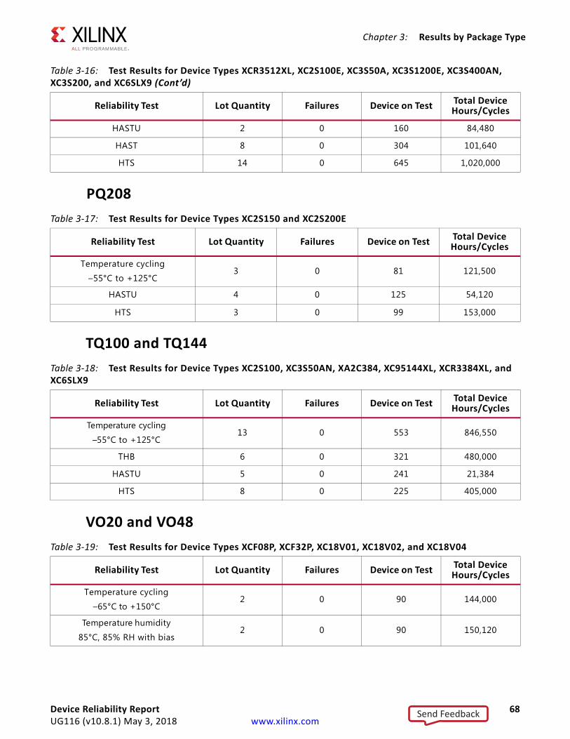
Chapter 3: Results by Package Type
PQ208
TQ100 and TQ144
VO20 and VO48
HASTU 2 0 160 84,480
HAST 8 0 304 101,640
HTS 14 0 645 1,020,000
Table 3-16: Test Results for Device Types XCR3512XL, XC2S100E, XC3S50A, XC3S1200E, XC3S400AN, XC3S200, and XC6SLX9 (Cont’d)
Reliability Test Lot Quantity Failures Device on Test Total Device Hours/Cycles
Table 3-17: Test Results for Device Types XC2S150 and XC2S200E
Reliability Test Lot Quantity Failures Device on Test Total Device Hours/Cycles
Temperature cycling
–55°C to +125°C3 0 81 121,500
HASTU 4 0 125 54,120
HTS 3 0 99 153,000
Table 3-18: Test Results for Device Types XC2S100, XC3S50AN, XA2C384, XC95144XL, XCR3384XL, and XC6SLX9
Reliability Test Lot Quantity Failures Device on Test Total Device Hours/Cycles
Temperature cycling
–55°C to +125°C13 0 553 846,550
THB 6 0 321 480,000
HASTU 5 0 241 21,384
HTS 8 0 225 405,000
Table 3-19: Test Results for Device Types XCF08P, XCF32P, XC18V01, XC18V02, and XC18V04
Reliability Test Lot Quantity Failures Device on Test Total Device Hours/Cycles
Temperature cycling
–65°C to +150°C2 0 90 144,000
Temperature humidity
85°C, 85% RH with bias2 0 90 150,120
Device Reliability Report 68UG116 (v10.8.1) May 3, 2018 www.xilinx.com
Send Feedback
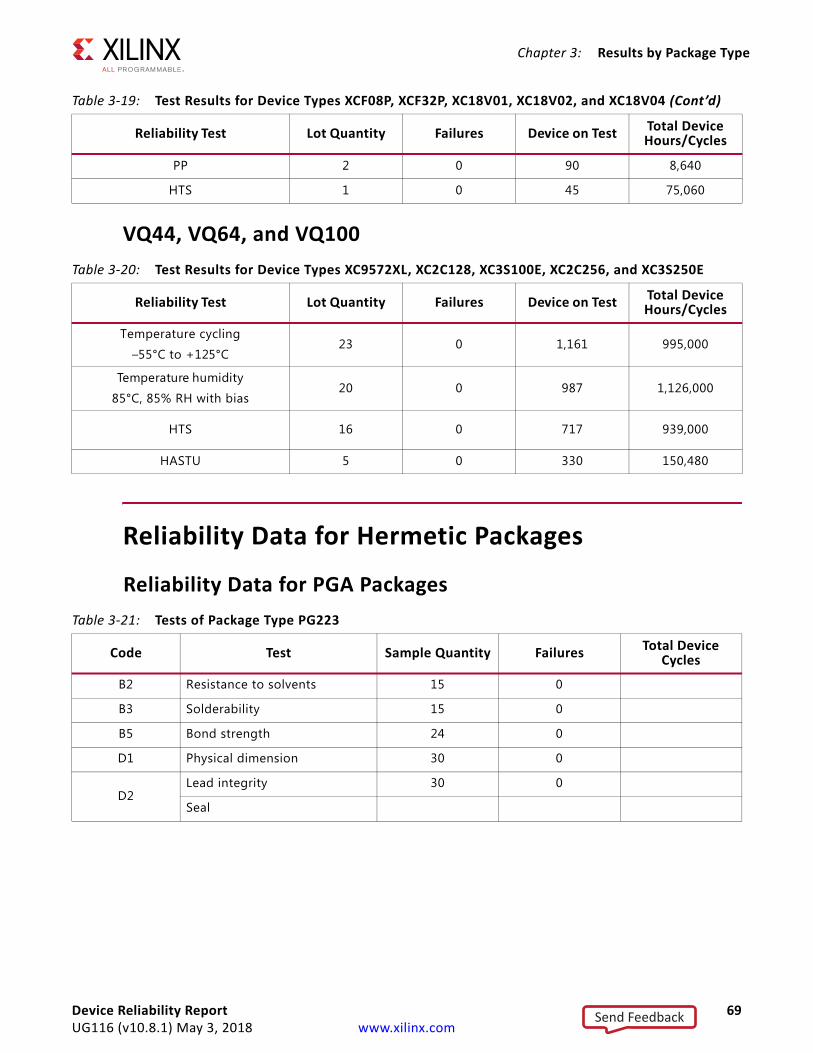
Chapter 3: Results by Package Type
VQ44, VQ64, and VQ100
Reliability Data for Hermetic Packages
Reliability Data for PGA Packages
PP 2 0 90 8,640
HTS 1 0 45 75,060
Table 3-19: Test Results for Device Types XCF08P, XCF32P, XC18V01, XC18V02, and XC18V04 (Cont’d)
Reliability Test Lot Quantity Failures Device on Test Total Device Hours/Cycles
Table 3-20: Test Results for Device Types XC9572XL, XC2C128, XC3S100E, XC2C256, and XC3S250E
Reliability Test Lot Quantity Failures Device on Test Total Device Hours/Cycles
Temperature cycling
–55°C to +125°C23 0 1,161 995,000
Temperature humidity
85°C, 85% RH with bias20 0 987 1,126,000
HTS 16 0 717 939,000
HASTU 5 0 330 150,480
Table 3-21: Tests of Package Type PG223
Code Test Sample Quantity Failures Total Device Cycles
B2 Resistance to solvents 15 0
B3 Solderability 15 0
B5 Bond strength 24 0
D1 Physical dimension 30 0
D2Lead integrity 30 0
Seal
Device Reliability Report 69UG116 (v10.8.1) May 3, 2018 www.xilinx.com
Send Feedback
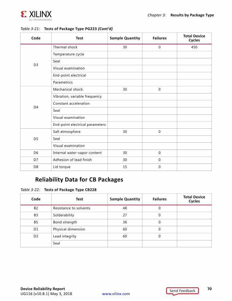
Chapter 3: Results by Package Type
Reliability Data for CB Packages
D3
Thermal shock 30 0 450
Temperature cycle
Seal
Visual examination
End-point electrical
Parametrics
D4
Mechanical shock 30 0
Vibration, variable frequency
Constant acceleration
Seal
Visual examination
End-point electrical parameters
D5
Salt atmosphere 30 0
Seal
Visual examination
D6 Internal water-vapor content 30 0
D7 Adhesion of lead finish 30 0
D8 Lid torque 15 0
Table 3-21: Tests of Package Type PG223 (Cont’d)
Code Test Sample Quantity Failures Total Device Cycles
Table 3-22: Tests of Package Type CB228
Code Test Sample Quantity Failures Total Device Cycles
B2 Resistance to solvents 48 0
B3 Solderability 27 0
B5 Bond strength 36 0
D1 Physical dimension 60 0
D2 Lead integrity 60 0
Seal
Device Reliability Report 70UG116 (v10.8.1) May 3, 2018 www.xilinx.com
Send Feedback
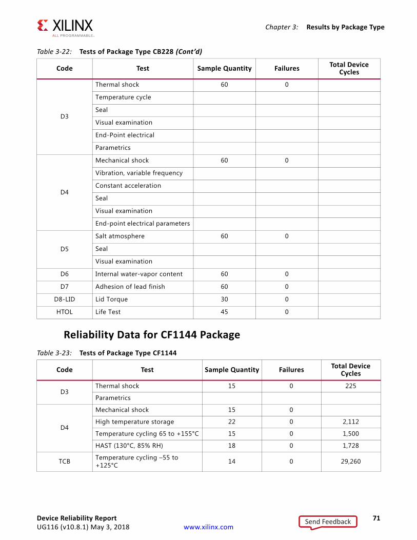
Chapter 3: Results by Package Type
Reliability Data for CF1144 Package
D3
Thermal shock 60 0
Temperature cycle
Seal
Visual examination
End-Point electrical
Parametrics
D4
Mechanical shock 60 0
Vibration, variable frequency
Constant acceleration
Seal
Visual examination
End-point electrical parameters
D5
Salt atmosphere 60 0
Seal
Visual examination
D6 Internal water-vapor content 60 0
D7 Adhesion of lead finish 60 0
D8-LID Lid Torque 30 0
HTOL Life Test 45 0
Table 3-22: Tests of Package Type CB228 (Cont’d)
Code Test Sample Quantity Failures Total Device Cycles
Table 3-23: Tests of Package Type CF1144
Code Test Sample Quantity Failures Total Device Cycles
D3Thermal shock 15 0 225
Parametrics
D4
Mechanical shock 15 0
High temperature storage 22 0 2,112
Temperature cycling 65 to +155°C 15 0 1,500
HAST (130°C, 85% RH) 18 0 1,728
TCB Temperature cycling –55 to +125°C 14 0 29,260
Device Reliability Report 71UG116 (v10.8.1) May 3, 2018 www.xilinx.com
Send Feedback
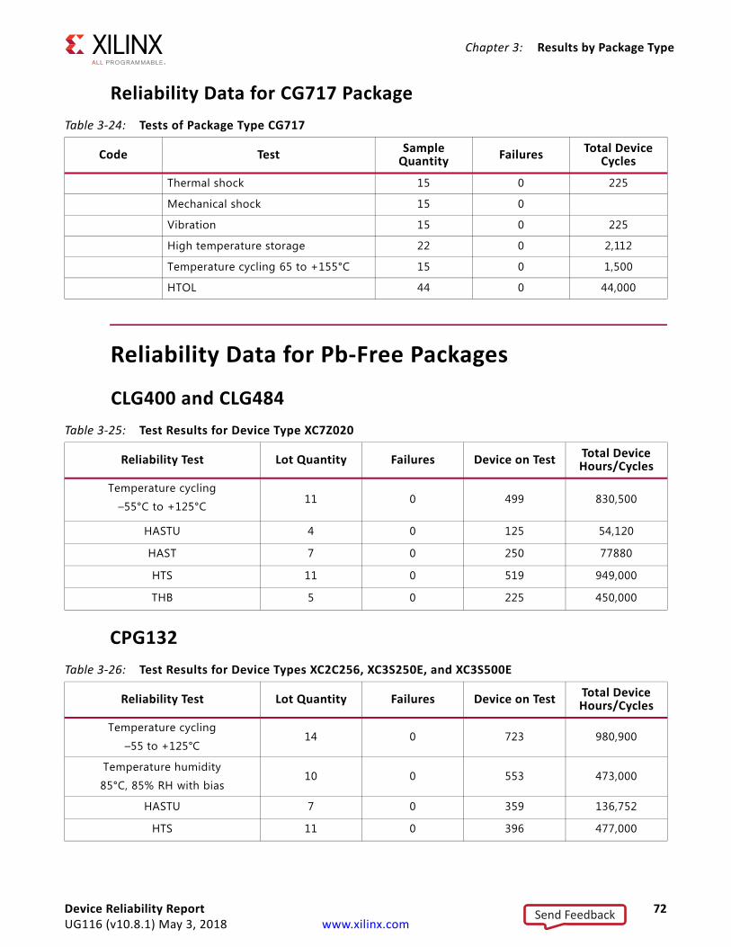
Chapter 3: Results by Package Type
Reliability Data for CG717 Package
Reliability Data for Pb-Free Packages
CLG400 and CLG484
CPG132
Table 3-24: Tests of Package Type CG717
Code Test Sample Quantity Failures Total Device
Cycles
Thermal shock 15 0 225
Mechanical shock 15 0
Vibration 15 0 225
High temperature storage 22 0 2,112
Temperature cycling 65 to +155°C 15 0 1,500
HTOL 44 0 44,000
Table 3-25: Test Results for Device Type XC7Z020
Reliability Test Lot Quantity Failures Device on Test Total Device Hours/Cycles
Temperature cycling
–55°C to +125°C11 0 499 830,500
HASTU 4 0 125 54,120
HAST 7 0 250 77880
HTS 11 0 519 949,000
THB 5 0 225 450,000
Table 3-26: Test Results for Device Types XC2C256, XC3S250E, and XC3S500E
Reliability Test Lot Quantity Failures Device on Test Total Device Hours/Cycles
Temperature cycling
–55 to +125°C14 0 723 980,900
Temperature humidity
85°C, 85% RH with bias10 0 553 473,000
HASTU 7 0 359 136,752
HTS 11 0 396 477,000
Device Reliability Report 72UG116 (v10.8.1) May 3, 2018 www.xilinx.com
Send Feedback
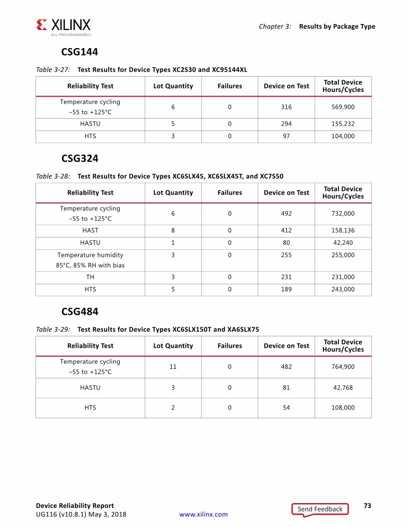
Chapter 3: Results by Package Type
CSG144
CSG324
CSG484
Table 3-27: Test Results for Device Types XC2S30 and XC95144XL
Reliability Test Lot Quantity Failures Device on Test Total Device Hours/Cycles
Temperature cycling
–55 to +125°C6 0 316 569,900
HASTU 5 0 294 155,232
HTS 3 0 97 104,000
Table 3-28: Test Results for Device Types XC6SLX45, XC6SLX45T, and XC7S50
Reliability Test Lot Quantity Failures Device on Test Total Device Hours/Cycles
Temperature cycling
–55 to +125°C6 0 492 732,000
HAST 8 0 412 158,136
HASTU 1 0 80 42,240
Temperature humidity
85°C, 85% RH with bias
3 0 255 255,000
TH 3 0 231 231,000
HTS 5 0 189 243,000
Table 3-29: Test Results for Device Types XC6SLX150T and XA6SLX75
Reliability Test Lot Quantity Failures Device on Test Total Device Hours/Cycles
Temperature cycling
–55 to +125°C11 0 482 764,900
HASTU 3 0 81 42,768
HTS 2 0 54 108,000
Device Reliability Report 73UG116 (v10.8.1) May 3, 2018 www.xilinx.com
Send Feedback
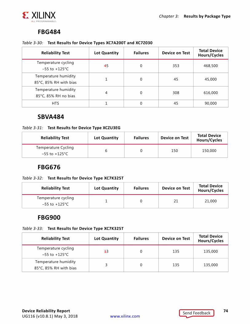
Chapter 3: Results by Package Type
FBG484
SBVA484
FBG676
FBG900
Table 3-30: Test Results for Device Types XC7A200T and XC7Z030
Reliability Test Lot Quantity Failures Device on Test Total Device Hours/Cycles
Temperature cycling
–55 to +125°C45 0 353 468,500
Temperature humidity
85°C, 85% RH with bias1 0 45 45,000
Temperature humidity
85°C, 85% RH no bias4 0 308 616,000
HTS 1 0 45 90,000
Table 3-31: Test Results for Device Type XCZU3EG
Reliability Test Lot Quantity Failures Device on Test Total Device Hours/Cycles
Temperature Cycling
–55 to +125°C6 0 150 150,000
Table 3-32: Test Results for Device Type XC7K325T
Reliability Test Lot Quantity Failures Device on Test Total Device Hours/Cycles
Temperature cycling
–55 to +125°C1 0 21 21,000
Table 3-33: Test Results for Device Type XC7K325T
Reliability Test Lot Quantity Failures Device on Test Total Device Hours/Cycles
Temperature cycling
–55 to +125°C13 0 135 135,000
Temperature humidity
85°C, 85% RH with bias3 0 135 135,000
Device Reliability Report 74UG116 (v10.8.1) May 3, 2018 www.xilinx.com
Send Feedback
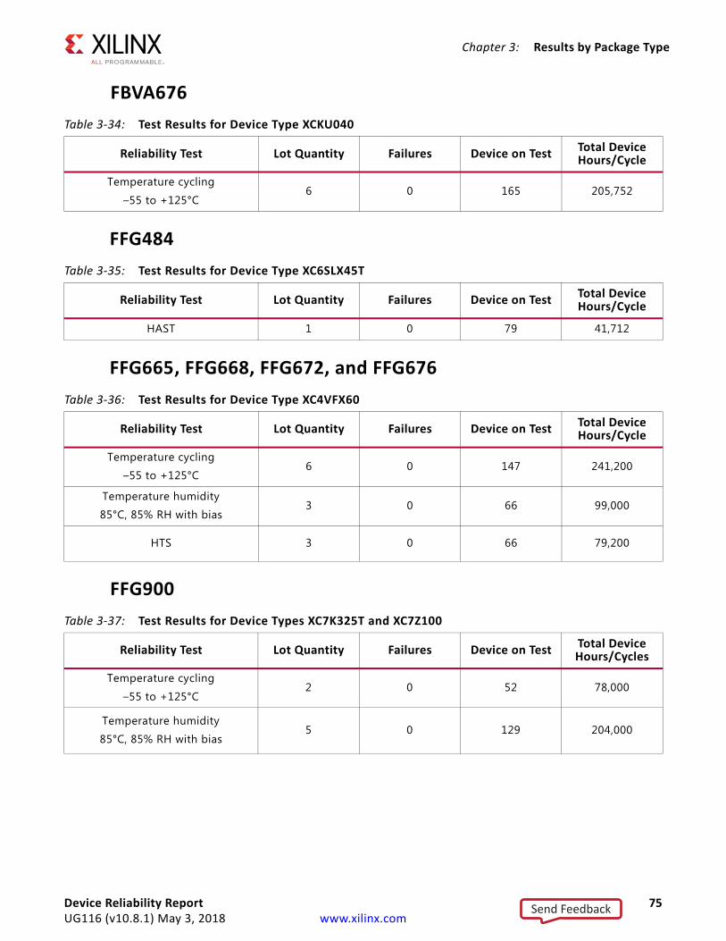
Chapter 3: Results by Package Type
FBVA676
FFG484
FFG665, FFG668, FFG672, and FFG676
FFG900
Table 3-34: Test Results for Device Type XCKU040
Reliability Test Lot Quantity Failures Device on Test Total Device Hours/Cycle
Temperature cycling
–55 to +125°C6 0 165 205,752
Table 3-35: Test Results for Device Type XC6SLX45T
Reliability Test Lot Quantity Failures Device on Test Total Device Hours/Cycle
HAST 1 0 79 41,712
Table 3-36: Test Results for Device Type XC4VFX60
Reliability Test Lot Quantity Failures Device on Test Total Device Hours/Cycle
Temperature cycling
–55 to +125°C6 0 147 241,200
Temperature humidity
85°C, 85% RH with bias3 0 66 99,000
HTS 3 0 66 79,200
Table 3-37: Test Results for Device Types XC7K325T and XC7Z100
Reliability Test Lot Quantity Failures Device on Test Total Device Hours/Cycles
Temperature cycling
–55 to +125°C2 0 52 78,000
Temperature humidity
85°C, 85% RH with bias5 0 129 204,000
Device Reliability Report 75UG116 (v10.8.1) May 3, 2018 www.xilinx.com
Send Feedback
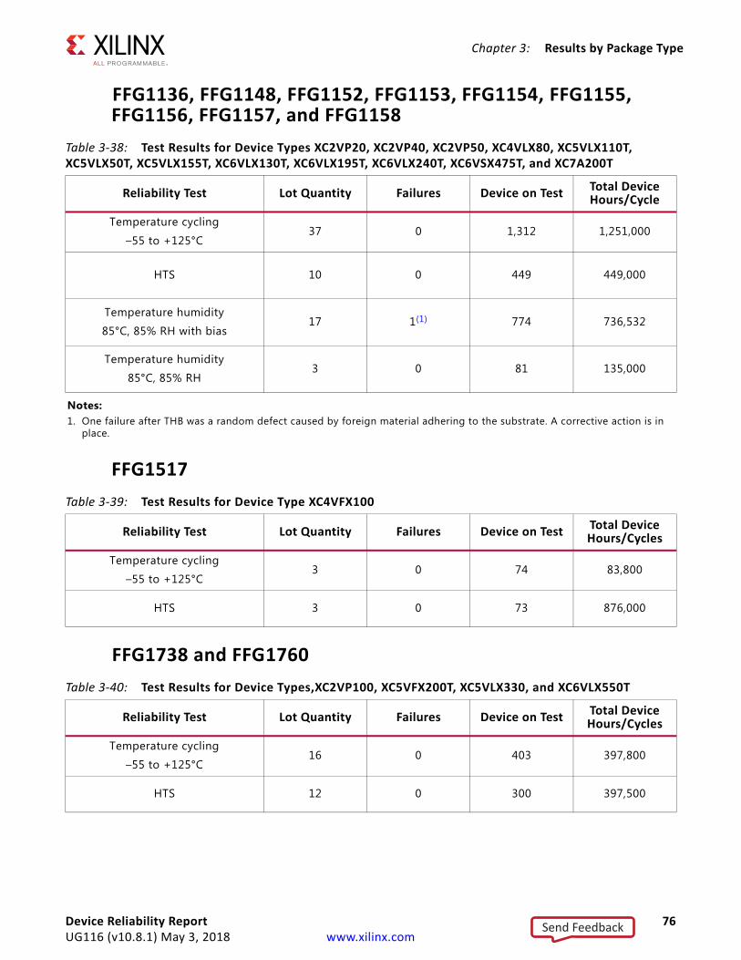
Chapter 3: Results by Package Type
FFG1136, FFG1148, FFG1152, FFG1153, FFG1154, FFG1155, FFG1156, FFG1157, and FFG1158
FFG1517
FFG1738 and FFG1760
Table 3-38: Test Results for Device Types XC2VP20, XC2VP40, XC2VP50, XC4VLX80, XC5VLX110T, XC5VLX50T, XC5VLX155T, XC6VLX130T, XC6VLX195T, XC6VLX240T, XC6VSX475T, and XC7A200T
Reliability Test Lot Quantity Failures Device on Test Total Device Hours/Cycle
Temperature cycling
–55 to +125°C37 0 1,312 1,251,000
HTS 10 0 449 449,000
Temperature humidity
85°C, 85% RH with bias17 1(1) 774 736,532
Temperature humidity
85°C, 85% RH3 0 81 135,000
Notes: 1. One failure after THB was a random defect caused by foreign material adhering to the substrate. A corrective action is in
place.
Table 3-39: Test Results for Device Type XC4VFX100
Reliability Test Lot Quantity Failures Device on Test Total Device Hours/Cycles
Temperature cycling
–55 to +125°C3 0 74 83,800
HTS 3 0 73 876,000
Table 3-40: Test Results for Device Types,XC2VP100, XC5VFX200T, XC5VLX330, and XC6VLX550T
Reliability Test Lot Quantity Failures Device on Test Total Device Hours/Cycles
Temperature cycling
–55 to +125°C16 0 403 397,800
HTS 12 0 300 397,500
Device Reliability Report 76UG116 (v10.8.1) May 3, 2018 www.xilinx.com
Send Feedback
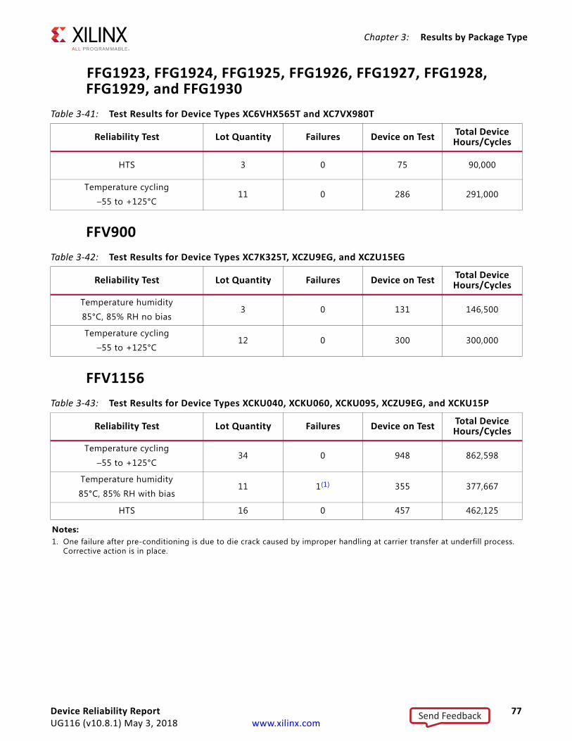
Chapter 3: Results by Package Type
FFG1923, FFG1924, FFG1925, FFG1926, FFG1927, FFG1928, FFG1929, and FFG1930
FFV900
FFV1156
Table 3-41: Test Results for Device Types XC6VHX565T and XC7VX980T
Reliability Test Lot Quantity Failures Device on Test Total Device Hours/Cycles
HTS 3 0 75 90,000
Temperature cycling
–55 to +125°C11 0 286 291,000
Table 3-42: Test Results for Device Types XC7K325T, XCZU9EG, and XCZU15EG
Reliability Test Lot Quantity Failures Device on Test Total Device Hours/Cycles
Temperature humidity
85°C, 85% RH no bias3 0 131 146,500
Temperature cycling
–55 to +125°C12 0 300 300,000
Table 3-43: Test Results for Device Types XCKU040, XCKU060, XCKU095, XCZU9EG, and XCKU15P
Reliability Test Lot Quantity Failures Device on Test Total Device Hours/Cycles
Temperature cycling
–55 to +125°C34 0 948 862,598
Temperature humidity
85°C, 85% RH with bias11 1(1) 355 377,667
HTS 16 0 457 462,125
Notes: 1. One failure after pre-conditioning is due to die crack caused by improper handling at carrier transfer at underfill process.
Corrective action is in place.
Device Reliability Report 77UG116 (v10.8.1) May 3, 2018 www.xilinx.com
Send Feedback
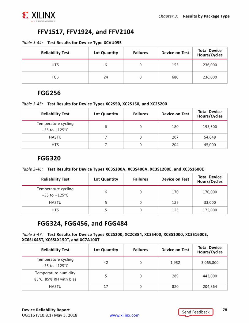
Chapter 3: Results by Package Type
FFV1517, FFV1924, and FFV2104
FGG256
FGG320
FGG324, FGG456, and FGG484
Table 3-44: Test Results for Device Type XCVU095
Reliability Test Lot Quantity Failures Device on Test Total Device Hours/Cycles
HTS 6 0 155 236,000
TCB 24 0 680 236,000
Table 3-45: Test Results for Device Types XC2S50, XC2S150, and XC2S200
Reliability Test Lot Quantity Failures Device on Test Total Device Hours/Cycles
Temperature cycling
–55 to +125°C6 0 180 193,500
HASTU 7 0 207 54,648
HTS 7 0 204 45,000
Table 3-46: Test Results for Device Types XC3S200A, XC3S400A, XC3S1200E, and XC3S1600E
Reliability Test Lot Quantity Failures Device on Test Total Device Hours/Cycles
Temperature cycling
–55 to +125°C6 0 170 170,000
HASTU 5 0 125 33,000
HTS 5 0 125 175,000
Table 3-47: Test Results for Device Types XC2S200, XC2C384, XC3S400, XC3S1000, XC3S1600E, XC6SLX45T, XC6SLX150T, and XC7A100T
Reliability Test Lot Quantity Failures Device on Test Total Device Hours/Cycles
Temperature cycling
–55 to +125°C42 0 1,952 3,065,800
Temperature humidity
85°C, 85% RH with bias5 0 289 443,000
HASTU 17 0 820 204,864
Device Reliability Report 78UG116 (v10.8.1) May 3, 2018 www.xilinx.com
Send Feedback
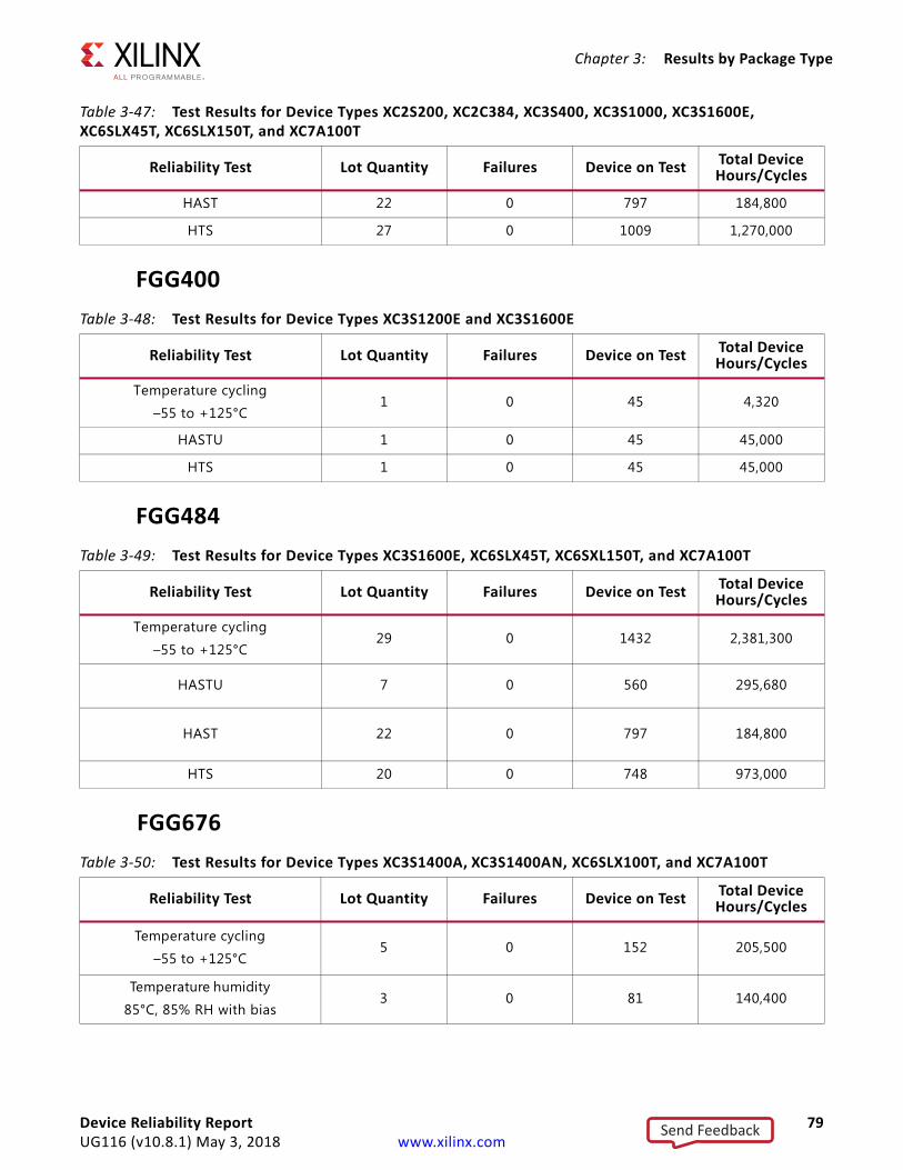
Chapter 3: Results by Package Type
FGG400
FGG484
FGG676
HAST 22 0 797 184,800
HTS 27 0 1009 1,270,000
Table 3-47: Test Results for Device Types XC2S200, XC2C384, XC3S400, XC3S1000, XC3S1600E, XC6SLX45T, XC6SLX150T, and XC7A100T
Reliability Test Lot Quantity Failures Device on Test Total Device Hours/Cycles
Table 3-48: Test Results for Device Types XC3S1200E and XC3S1600E
Reliability Test Lot Quantity Failures Device on Test Total Device Hours/Cycles
Temperature cycling
–55 to +125°C1 0 45 4,320
HASTU 1 0 45 45,000
HTS 1 0 45 45,000
Table 3-49: Test Results for Device Types XC3S1600E, XC6SLX45T, XC6SXL150T, and XC7A100T
Reliability Test Lot Quantity Failures Device on Test Total Device Hours/Cycles
Temperature cycling
–55 to +125°C29 0 1432 2,381,300
HASTU 7 0 560 295,680
HAST 22 0 797 184,800
HTS 20 0 748 973,000
Table 3-50: Test Results for Device Types XC3S1400A, XC3S1400AN, XC6SLX100T, and XC7A100T
Reliability Test Lot Quantity Failures Device on Test Total Device Hours/Cycles
Temperature cycling
–55 to +125°C5 0 152 205,500
Temperature humidity
85°C, 85% RH with bias3 0 81 140,400
Device Reliability Report 79UG116 (v10.8.1) May 3, 2018 www.xilinx.com
Send Feedback
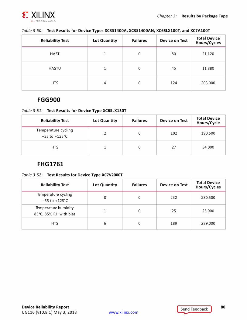
Chapter 3: Results by Package Type
FGG900
FHG1761
HAST 1 0 80 21,120
HASTU 1 0 45 11,880
HTS 4 0 124 203,000
Table 3-50: Test Results for Device Types XC3S1400A, XC3S1400AN, XC6SLX100T, and XC7A100T
Reliability Test Lot Quantity Failures Device on Test Total Device Hours/Cycles
Table 3-51: Test Results for Device Type XC6SLX150T
Reliability Test Lot Quantity Failures Device on Test Total Device Hours/Cycle
Temperature cycling
–55 to +125°C2 0 102 190,500
HTS 1 0 27 54,000
Table 3-52: Test Results for Device Type XC7V2000T
Reliability Test Lot Quantity Failures Device on Test Total Device Hours/Cycles
Temperature cycling
–55 to +125°C8 0 232 280,500
Temperature humidity
85°C, 85% RH with bias1 0 25 25,000
HTS 6 0 189 289,000
Device Reliability Report 80UG116 (v10.8.1) May 3, 2018 www.xilinx.com
Send Feedback
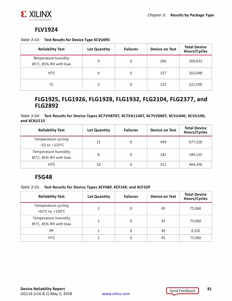
Chapter 3: Results by Package Type
FLV1924
FLG1925, FLG1926, FLG1928, FLG1932, FLG2104, FLG2377, and FLG2892
FSG48
Table 3-53: Test Results for Device Type XCVU095
Reliability Test Lot Quantity Failures Device on Test Total Device Hours/Cycles
Temperature humidity
85°C, 85% RH with bias9 0 266 269,632
HTS 4 0 157 202,048
TC 3 0 133 221,500
Table 3-54: Test Results for Device Types XC7VH870T, XC7VX1140T, XC7V2000T, XCVU440, XCVU190, and XCKU115
Reliability Test Lot Quantity Failures Device on Test Total Device Hours/Cycles
Temperature cycling
–55 to +125°C21 0 499 677,520
Temperature humidity
85°C, 85% RH with bias8 0 181 184,155
HTS 10 0 311 464,336
Table 3-55: Test Results for Device Types XCF08P, XCF16P, and XCF32P
Reliability Test Lot Quantity Failures Device on Test Total Device Hours/Cycles
Temperature cycling
–65°C to +150°C1 0 45 75,060
Temperature humidity
85°C, 85% RH with bias1 0 45 75,060
PP 1 0 45 4,320
HTS 1 0 45 75,060
Device Reliability Report 81UG116 (v10.8.1) May 3, 2018 www.xilinx.com
Send Feedback
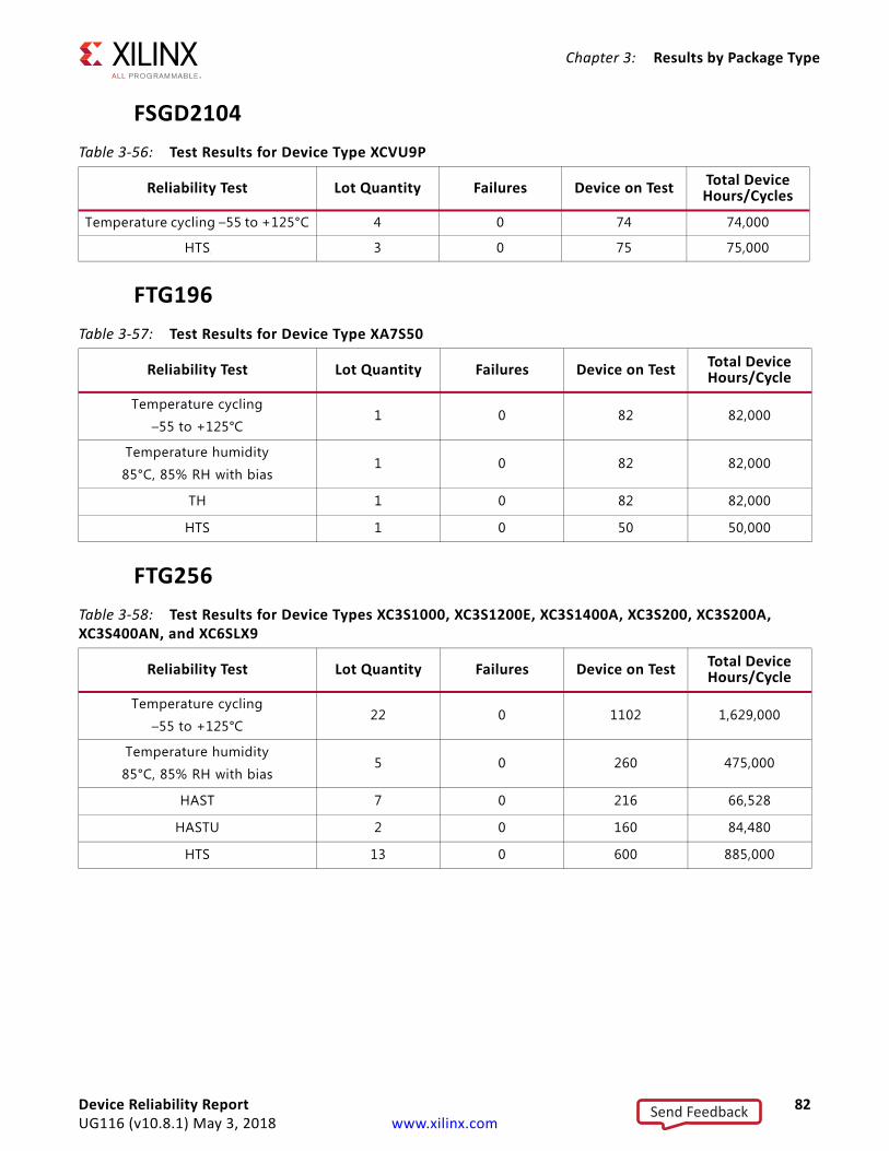
Chapter 3: Results by Package Type
FSGD2104
FTG196
FTG256
Table 3-56: Test Results for Device Type XCVU9P
Reliability Test Lot Quantity Failures Device on Test Total Device Hours/Cycles
Temperature cycling –55 to +125°C 4 0 74 74,000
HTS 3 0 75 75,000
Table 3-57: Test Results for Device Type XA7S50
Reliability Test Lot Quantity Failures Device on Test Total Device Hours/Cycle
Temperature cycling
–55 to +125°C1 0 82 82,000
Temperature humidity
85°C, 85% RH with bias1 0 82 82,000
TH 1 0 82 82,000
HTS 1 0 50 50,000
Table 3-58: Test Results for Device Types XC3S1000, XC3S1200E, XC3S1400A, XC3S200, XC3S200A, XC3S400AN, and XC6SLX9
Reliability Test Lot Quantity Failures Device on Test Total Device Hours/Cycle
Temperature cycling
–55 to +125°C22 0 1102 1,629,000
Temperature humidity
85°C, 85% RH with bias5 0 260 475,000
HAST 7 0 216 66,528
HASTU 2 0 160 84,480
HTS 13 0 600 885,000
Device Reliability Report 82UG116 (v10.8.1) May 3, 2018 www.xilinx.com
Send Feedback
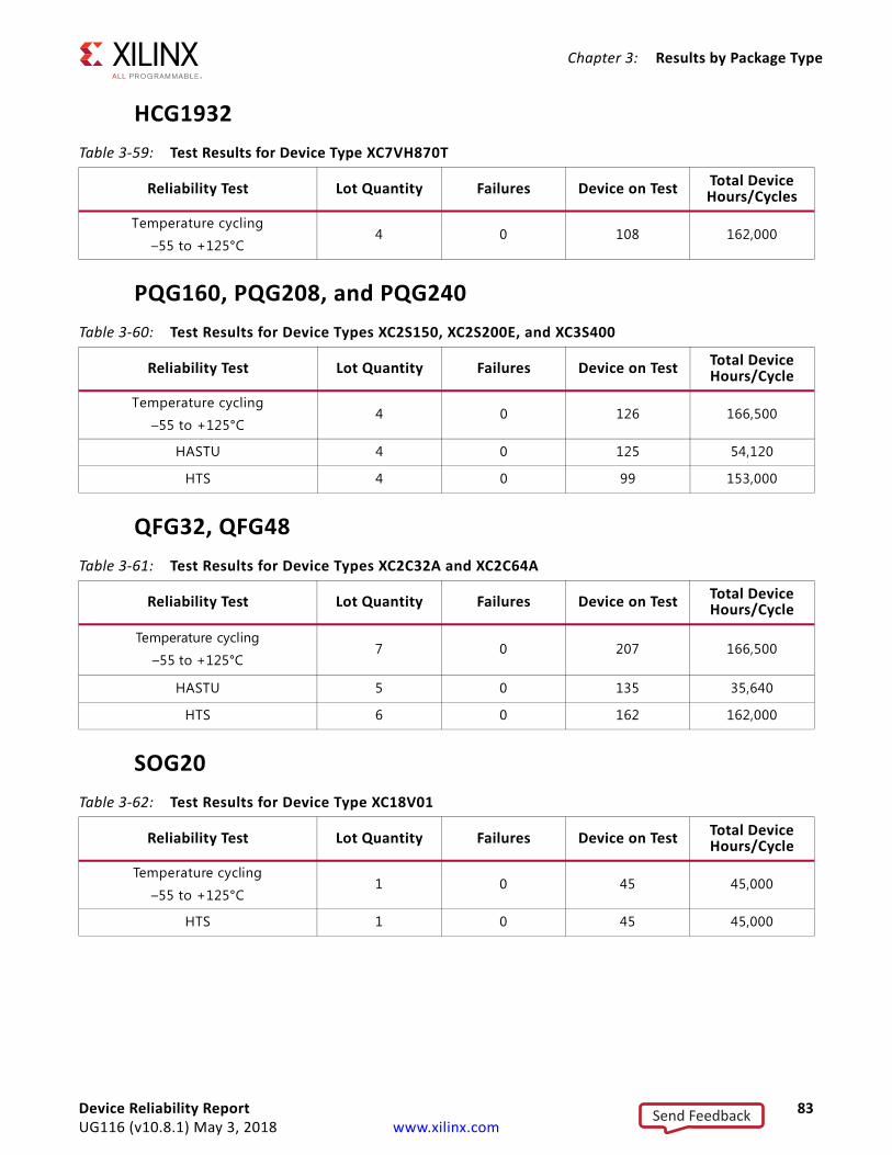
Chapter 3: Results by Package Type
HCG1932
PQG160, PQG208, and PQG240
QFG32, QFG48
SOG20
Table 3-59: Test Results for Device Type XC7VH870T
Reliability Test Lot Quantity Failures Device on Test Total Device Hours/Cycles
Temperature cycling
–55 to +125°C4 0 108 162,000
Table 3-60: Test Results for Device Types XC2S150, XC2S200E, and XC3S400
Reliability Test Lot Quantity Failures Device on Test Total Device Hours/Cycle
Temperature cycling
–55 to +125°C4 0 126 166,500
HASTU 4 0 125 54,120
HTS 4 0 99 153,000
Table 3-61: Test Results for Device Types XC2C32A and XC2C64A
Reliability Test Lot Quantity Failures Device on Test Total Device Hours/Cycle
Temperature cycling
–55 to +125°C7 0 207 166,500
HASTU 5 0 135 35,640
HTS 6 0 162 162,000
Table 3-62: Test Results for Device Type XC18V01
Reliability Test Lot Quantity Failures Device on Test Total Device Hours/Cycle
Temperature cycling
–55 to +125°C1 0 45 45,000
HTS 1 0 45 45,000
Device Reliability Report 83UG116 (v10.8.1) May 3, 2018 www.xilinx.com
Send Feedback
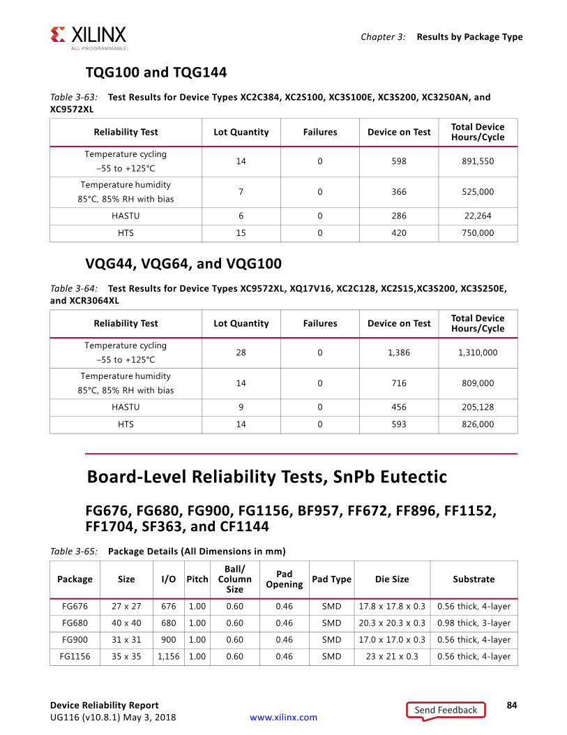
Chapter 3: Results by Package Type
TQG100 and TQG144
VQG44, VQG64, and VQG100
Board-Level Reliability Tests, SnPb Eutectic
FG676, FG680, FG900, FG1156, BF957, FF672, FF896, FF1152, FF1704, SF363, and CF1144
Table 3-63: Test Results for Device Types XC2C384, XC2S100, XC3S100E, XC3S200, XC3250AN, and XC9572XL
Reliability Test Lot Quantity Failures Device on Test Total Device Hours/Cycle
Temperature cycling
–55 to +125°C14 0 598 891,550
Temperature humidity
85°C, 85% RH with bias7 0 366 525,000
HASTU 6 0 286 22,264
HTS 15 0 420 750,000
Table 3-64: Test Results for Device Types XC9572XL, XQ17V16, XC2C128, XC2S15,XC3S200, XC3S250E, and XCR3064XL
Reliability Test Lot Quantity Failures Device on Test Total Device Hours/Cycle
Temperature cycling
–55 to +125°C28 0 1,386 1,310,000
Temperature humidity
85°C, 85% RH with bias14 0 716 809,000
HASTU 9 0 456 205,128
HTS 14 0 593 826,000
Table 3-65: Package Details (All Dimensions in mm)
Package Size I/O PitchBall/
Column Size
Pad Opening Pad Type Die Size Substrate
FG676 27 x 27 676 1.00 0.60 0.46 SMD 17.8 x 17.8 x 0.3 0.56 thick, 4-layer
FG680 40 x 40 680 1.00 0.60 0.46 SMD 20.3 x 20.3 x 0.3 0.98 thick, 3-layer
FG900 31 x 31 900 1.00 0.60 0.46 SMD 17.0 x 17.0 x 0.3 0.56 thick, 4-layer
FG1156 35 x 35 1,156 1.00 0.60 0.46 SMD 23 x 21 x 0.3 0.56 thick, 4-layer
Device Reliability Report 84UG116 (v10.8.1) May 3, 2018 www.xilinx.com
Send Feedback
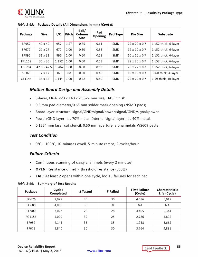
Chapter 3: Results by Package Type
Mother Board Design and Assembly Details
• 8-layer, FR-4, 220 x 140 x 2.3622 mm size, HASL finish
• 0.5 mm pad diameter/0.65 mm solder mask opening (NSMD pads)
• Board layer structure: signal/GND/signal/power/signal/GND/signal/power
• Power/GND layer has 70% metal. Internal signal layer has 40% metal.
• 0.1524 mm laser cut stencil, 0.50 mm aperture, alpha metals WS609 paste
Test Condition
• 0°C – 100°C, 10-minutes dwell, 5-minute ramps, 2 cycles/hour
Failure Criteria
• Continuous scanning of daisy chain nets (every 2 minutes)
• OPEN: Resistance of net > threshold resistance (300Ω )
• FAIL: At least 2 opens within one cycle, log 15 failures for each net
BF957 40 x 40 957 1.27 0.75 0.61 SMD 22 x 20 x 0.7 1.152 thick, 6-layer
FF672 27 x 27 672 1.00 0.60 0.53 SMD 12 x 10 x 0.7 1.152 thick, 6-layer
FF896 31 x 31 896 1.00 0.60 0.53 SMD 10 x 10 x 0.7 1.152 thick, 6-layer
FF1152 35 x 35 1,152 1.00 0.60 0.53 SMD 22 x 20 x 0.7 1.152 thick, 6-layer
FF1704 42.5 x 42.5 1,704 1.00 0.60 0.53 SMD 26 x 22 x 0.7 1.152 thick, 6-layer
SF363 17 x 17 363 0.8 0.50 0.40 SMD 10 x 10 x 0.3 0.60 thick, 4-layer
CF1144 35 x 35 1,144 1.00 0.52 0.80 SMD 22 x 20 x 0.7 1.59 thick, 10-layer
Table 3-65: Package Details (All Dimensions in mm) (Cont’d)
Package Size I/O PitchBall/
Column Size
Pad Opening Pad Type Die Size Substrate
Table 3-66: Summary of Test Results
Package Cycles Completed # Tested # Failed First Failure
(Cycle)Characteristic
Life (Cycle)
FG676 7,027 30 30 4,686 6,012
FG680 4,000 30 0 NA NA
FG900 7,027 28 28 4,405 5,344
FG1156 5,000 32 25 2,786 4,892
BF957 4,145 35 35 1,958 3,662
FF672 5,840 30 30 3,764 4,881
Device Reliability Report 85UG116 (v10.8.1) May 3, 2018 www.xilinx.com
Send Feedback
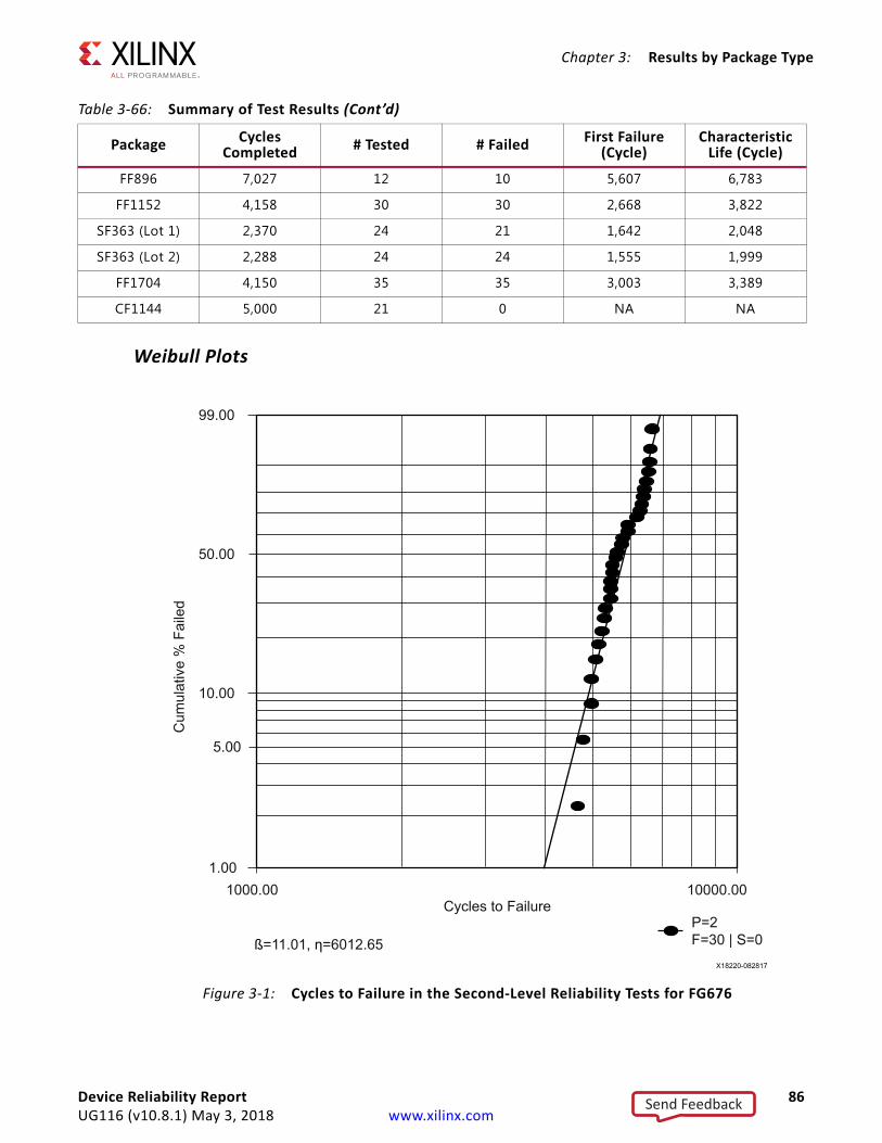
Chapter 3: Results by Package Type
Weibull Plots
FF896 7,027 12 10 5,607 6,783
FF1152 4,158 30 30 2,668 3,822
SF363 (Lot 1) 2,370 24 21 1,642 2,048
SF363 (Lot 2) 2,288 24 24 1,555 1,999
FF1704 4,150 35 35 3,003 3,389
CF1144 5,000 21 0 NA NA
Table 3-66: Summary of Test Results (Cont’d)
Package Cycles Completed # Tested # Failed First Failure
(Cycle)Characteristic
Life (Cycle)
X-Ref Target - Figure 3-1
Figure 3-1: Cycles to Failure in the Second-Level Reliability Tests for FG676
1.00
5.00
10.00
50.00
99.00
1000.00 10000.00Cycles to Failure
Cum
ulat
ive
% F
aile
d
P=2F=30 | S=0ß=11.01, η=6012.65
X18220-082817
Device Reliability Report 86UG116 (v10.8.1) May 3, 2018 www.xilinx.com
Send Feedback
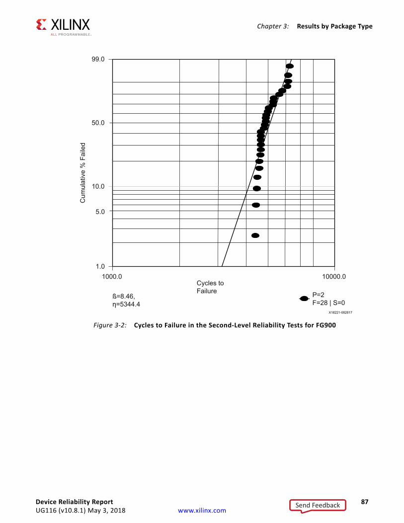
Chapter 3: Results by Package Type
X-Ref Target - Figure 3-2
Figure 3-2: Cycles to Failure in the Second-Level Reliability Tests for FG900
1000.0 10000.0Cycles to Failure
Cum
ulat
ive
% F
aile
d
P=2F=28 | S=0
1.0
5.0
10.0
50.0
99.0
ß=8.46, η=5344.4
X18221-082817
Device Reliability Report 87UG116 (v10.8.1) May 3, 2018 www.xilinx.com
Send Feedback
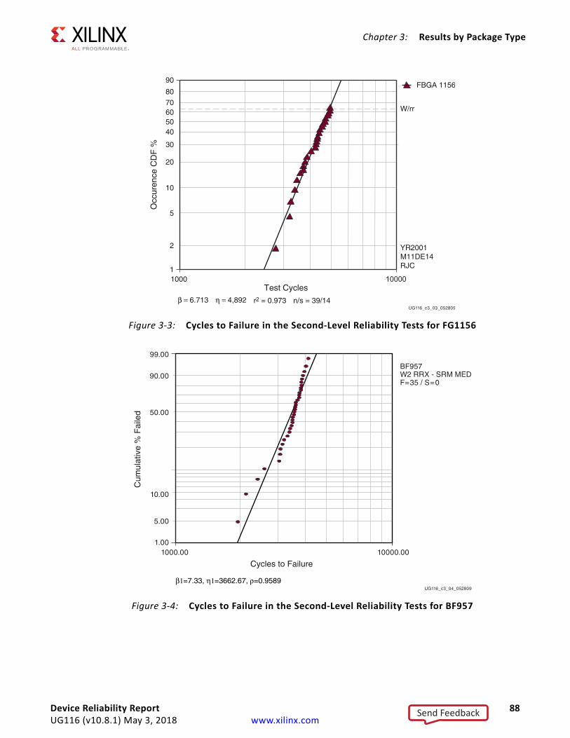
Chapter 3: Results by Package Type
X-Ref Target - Figure 3-3
Figure 3-3: Cycles to Failure in the Second-Level Reliability Tests for FG1156X-Ref Target - Figure 3-4
Figure 3-4: Cycles to Failure in the Second-Level Reliability Tests for BF957
UG116_c3_03_052809
1000 100001
5
40
30
20
10
80
70W/rr60
50
90
Test Cycles
Occ
uren
ce C
DF
%
FBGA 1156
β = 6.713
YR2001M11DE14RJC
2
r2 = 0.973 n/s = 39/14η = 4,892
99.00
90.00
50.00
10.00
5.00
1.001000.00 10000.00
Cycles to Failure
Cum
ulat
ive
% F
aile
d
β1=7.33, η1=3662.67, ρ=0.9589
BF957
F=35 / S=0W2 RRX - SRM MED
UG116_c3_04_052809
Device Reliability Report 88UG116 (v10.8.1) May 3, 2018 www.xilinx.com
Send Feedback
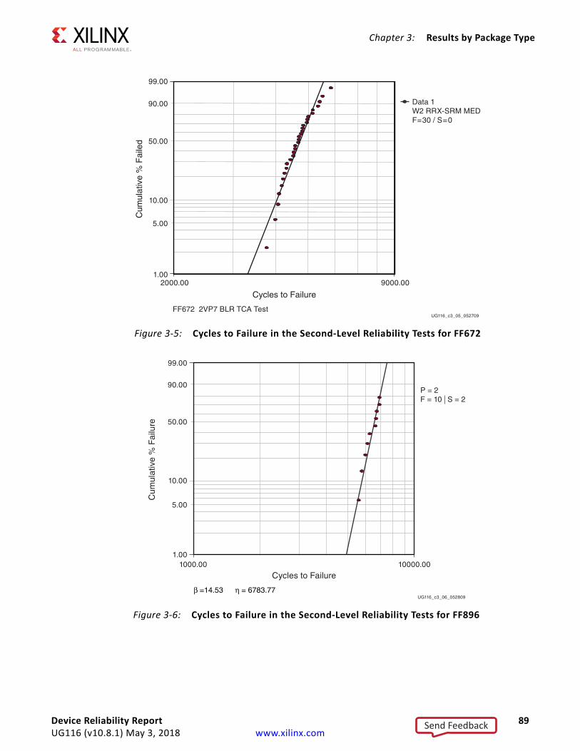
Chapter 3: Results by Package Type
X-Ref Target - Figure 3-5
Figure 3-5: Cycles to Failure in the Second-Level Reliability Tests for FF672X-Ref Target - Figure 3-6
Figure 3-6: Cycles to Failure in the Second-Level Reliability Tests for FF896
UG116_c3_05_052709
Data 1W2 RRX-SRM MEDF=30 / S=0
99.00
90.00
50.00
10.00
5.00
1.00
Cum
ulat
ive
% F
aile
d
2000.00 9000.00
FF672 2VP7 BLR TCA Test
Cycles to Failure
99.00
90.00
50.00
10.00
5.00
1.001000.00 10000.00
Cycles to Failure
Cum
ulat
ive
% F
ailu
re
β =14.53
P = 2F = 10 S = 2
UG116_c3_06_052809η = 6783.77
Device Reliability Report 89UG116 (v10.8.1) May 3, 2018 www.xilinx.com
Send Feedback
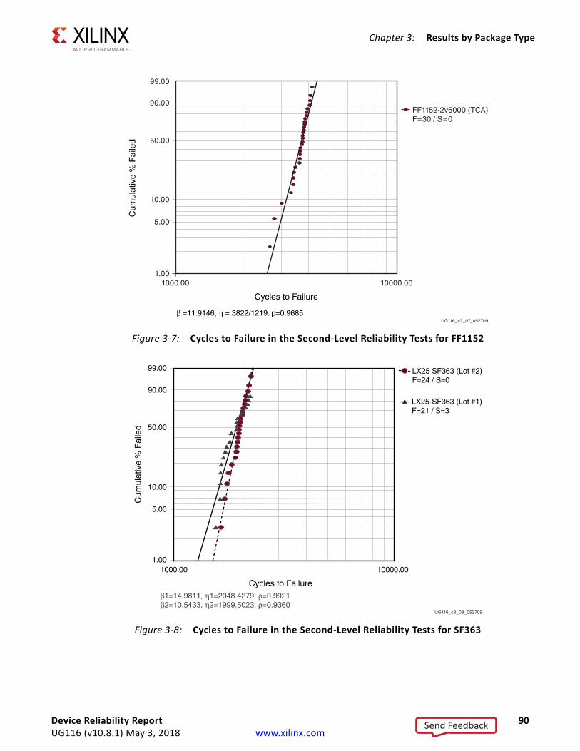
Chapter 3: Results by Package Type
X-Ref Target - Figure 3-7
Figure 3-7: Cycles to Failure in the Second-Level Reliability Tests for FF1152X-Ref Target - Figure 3-8
Figure 3-8: Cycles to Failure in the Second-Level Reliability Tests for SF363
99.00
90.00
50.00
10.00
5.00
1.001000.00 10000.00
Cycles to Failure
Cum
ulat
ive
% F
aile
d
UG116_c3_07_052709
β =11.9146, η = 3822/1219. p=0.9685
FF1152-2v6000 (TCA)F=30 / S=0
UG116_c3_08_052709
1000.00 10000.001.00
5.00
10.00
LX25 SF363 (Lot #2)F=24 / S=0
β1=14.9811, η1=2048.4279, ρ=0.9921β2=10.5433, η2=1999.5023, ρ=0.9360
LX25-SF363 (Lot #1)F=21 / S=3
50.00
90.00
99.00
Cycles to Failure
Cum
ulat
ive
% F
aile
d
Device Reliability Report 90UG116 (v10.8.1) May 3, 2018 www.xilinx.com
Send Feedback
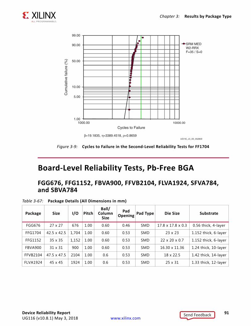
Chapter 3: Results by Package Type
Board-Level Reliability Tests, Pb-Free BGA
FGG676, FFG1152, FBVA900, FFVB2104, FLVA1924, SFVA784, and SBVA784
X-Ref Target - Figure 3-9
Figure 3-9: Cycles to Failure in the Second-Level Reliability Tests for FF1704
10000.001.00
5.00
10.00
50.00
90.00
99.00
Cycles to Failure
β=19.1835, η=3389.4518, ρ=0.8659
1000.00
Cum
ulat
ive
failu
re (
%)
SRM MEDW2-RRXF=35 / S=0
UG116_c3_09_052809
Table 3-67: Package Details (All Dimensions in mm)
Package Size I/O PitchBall/
Column Size
Pad Opening Pad Type Die Size Substrate
FGG676 27 x 27 676 1.00 0.60 0.46 SMD 17.8 x 17.8 x 0.3 0.56 thick, 4-layer
FFG1704 42.5 x 42.5 1,704 1.00 0.60 0.53 SMD 23 x 23 1.152 thick, 6-layer
FFG1152 35 x 35 1,152 1.00 0.60 0.53 SMD 22 x 20 x 0.7 1.152 thick, 6-layer
FBVA900 31 x 31 900 1.00 0.60 0.53 SMD 16.30 x 11.36 1.24 thick, 10-layer
FFVB2104 47.5 x 47.5 2104 1.00 0.6 0.53 SMD 18 x 22.5 1.42 thick, 14-layer
FLVA1924 45 x 45 1924 1.00 0.6 0.53 SMD 25 x 31 1.33 thick, 12-layer
Device Reliability Report 91UG116 (v10.8.1) May 3, 2018 www.xilinx.com
Send Feedback
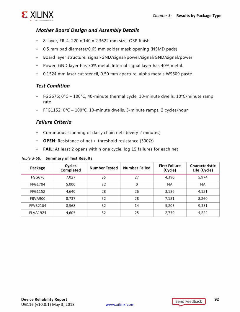
Chapter 3: Results by Package Type
Mother Board Design and Assembly Details
• 8-layer, FR-4, 220 x 140 x 2.3622 mm size, OSP finish
• 0.5 mm pad diameter/0.65 mm solder mask opening (NSMD pads)
• Board layer structure: signal/GND/signal/power/signal/GND/signal/power
• Power, GND layer has 70% metal. Internal signal layer has 40% metal.
• 0.1524 mm laser cut stencil, 0.50 mm aperture, alpha metals WS609 paste
Test Condition
• FGG676: 0°C – 100°C, 40-minute thermal cycle, 10-minute dwells, 10°C/minute ramp rate
• FFG1152: 0°C – 100°C, 10-minute dwells, 5-minute ramps, 2 cycles/hour
Failure Criteria
• Continuous scanning of daisy chain nets (every 2 minutes)
• OPEN: Resistance of net > threshold resistance (300Ω )
• FAIL: At least 2 opens within one cycle, log 15 failures for each net
Table 3-68: Summary of Test Results
Package Cycles Completed Number Tested Number Failed First Failure
(Cycle)Characteristic
Life (Cycle)
FGG676 7,027 35 27 4,390 5,974
FFG1704 5,000 32 0 NA NA
FFG1152 4,640 28 26 3,186 4,121
FBVA900 8,737 32 28 7,181 8,260
FFVB2104 8,568 32 14 5,205 9,351
FLVA1924 4,605 32 25 2,759 4,222
Device Reliability Report 92UG116 (v10.8.1) May 3, 2018 www.xilinx.com
Send Feedback
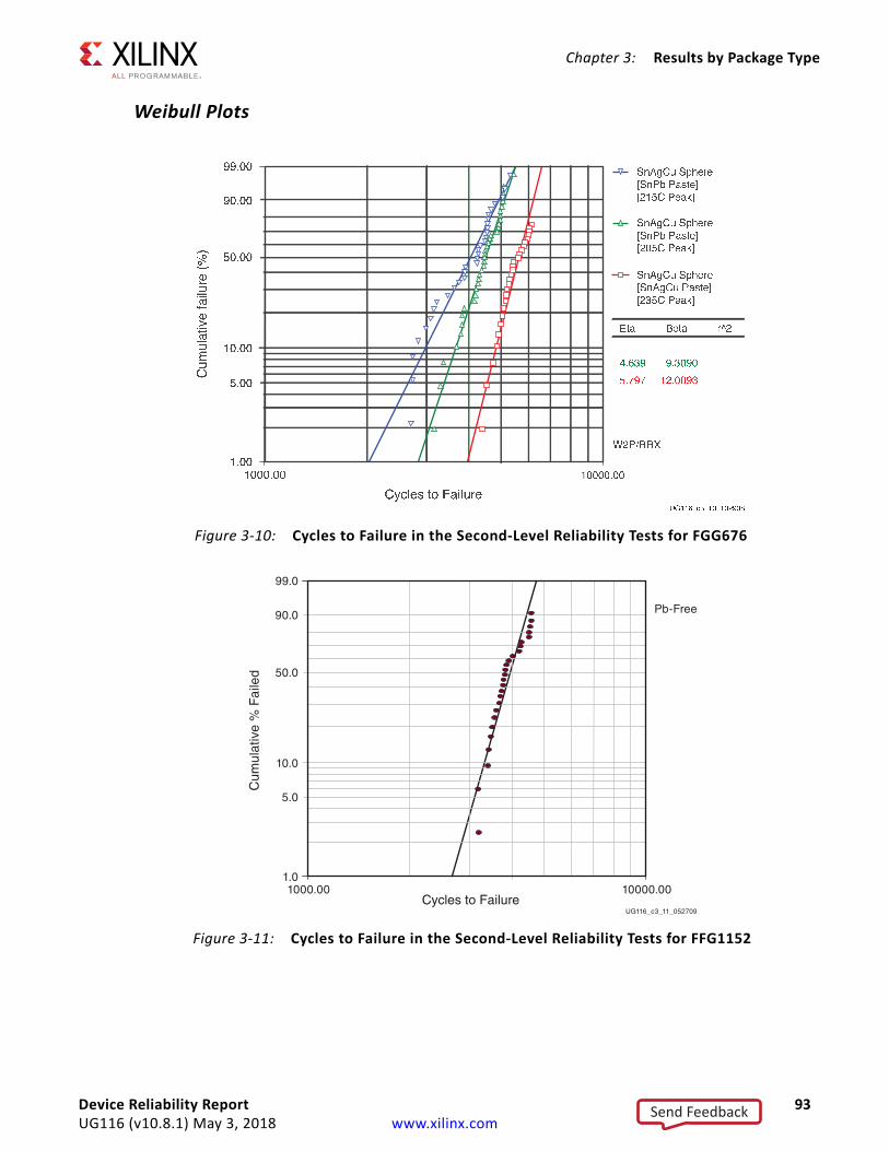
Chapter 3: Results by Package Type
Weibull PlotsX-Ref Target - Figure 3-10
Figure 3-10: Cycles to Failure in the Second-Level Reliability Tests for FGG676X-Ref Target - Figure 3-11
Figure 3-11: Cycles to Failure in the Second-Level Reliability Tests for FFG1152
��������������
�� ����������� ��������������������
�� ������������������������������
��������
�����
���������������
�� !�� �" #�$!����������
��%�!��$&��'�
$!����()*
+,��-. �.��.�����/
�� ������������������������������
0�� 1���2�-�� ��������3�3 �������
�4�
UG116_c3_11_052709
Pb-Free
99.0
90.0
50.0
10.0
5.0
1.0
Cum
ulat
ive
% F
aile
d
1000.00 10000.00Cycles to Failure
Device Reliability Report 93UG116 (v10.8.1) May 3, 2018 www.xilinx.com
Send Feedback
Chapter 3: Results by Package Type
FBG900
Mother Board Design and Assembly Details
• 8-layer, FR-4, 220 x 140 x 2.36 mm size, ENIG finish
• 0.45 mm pad diameter/0.55 mm solder mask opening (NSMD pads)
• Board layer structure: signal/GND/signal/power/signal/GND/signal/power
• Power, GND layer has 70% metal. Internal signal layer has 40% metal.
• 0.127 mm laser cut stencil, 0.50 mm aperture, alpha metals WS820 paste
Test Condition
• 0°C–100°C, 40-minute thermal cycle, 10-minute dwells, 10°C/minute ramp rate
Failure Criteria
• Continuous scanning of daisy chain nets with event detection
• FAIL: Resistance of net > threshold resistance (500Ω ), 10 events (maximum), 1 μs duration (maximum)
Table 3-69: Package Details (All Dimensions in mm)
Package Size I/O Pitch Ball/Column Size Pad Opening Pad Type Die Size Substrate
FBG900 31 X 31 900 1.00 0.60 0.53 SMD 12.93 x 16.91 0.95 thick, 8-layer
Table 3-70: Summary of Test Results
Package Cycles Completed Number Tested Number Failed First Failure (Cycle) Characteristic Life (Cycle)
FBG900 10,085 32 18 5,674 9,148
Device Reliability Report 94UG116 (v10.8.1) May 3, 2018 www.xilinx.com
Send Feedback
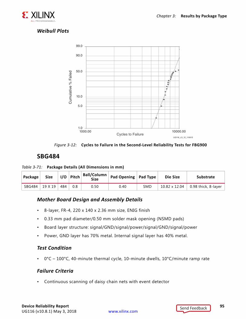
Chapter 3: Results by Package Type
Weibull Plots
SBG484
Mother Board Design and Assembly Details
• 8-layer, FR-4, 220 x 140 x 2.36 mm size, ENIG finish
• 0.33 mm pad diameter/0.50 mm solder mask opening (NSMD pads)
• Board layer structure: signal/GND/signal/power/signal/GND/signal/power
• Power, GND layer has 70% metal. Internal signal layer has 40% metal.
Test Condition
• 0°C – 100°C, 40-minute thermal cycle, 10-minute dwells, 10°C/minute ramp rate
Failure Criteria
• Continuous scanning of daisy chain nets with event detector
X-Ref Target - Figure 3-12
Figure 3-12: Cycles to Failure in the Second-Level Reliability Tests for FBG900
UG116_c3_12_110613
99.0
90.0
50.0
10.0
5.0
1.0
Cum
ulat
ive
% F
aile
d
1000.00 10000.00Cycles to Failure
Table 3-71: Package Details (All Dimensions in mm)
Package Size I/O Pitch Ball/Column Size Pad Opening Pad Type Die Size Substrate
SBG484 19 X 19 484 0.8 0.50 0.40 SMD 10.82 x 12.04 0.98 thick, 8-layer
Device Reliability Report 95UG116 (v10.8.1) May 3, 2018 www.xilinx.com
Send Feedback
Chapter 3: Results by Package Type
• FAIL: Resistance of net > threshold resistance (500Ω ), 10 events (maximum), 1 μs duration (maximum)
Weibull Plots
FFG1928
Mother Board Design and Assembly Details
• 16-layer, FR-4, 220 x 140 x 2.4 mm size, OSP finish
• 0.53 mm pad diameter/0.63 mm solder mask opening (NSMD pads)
• Board layer structure: signal/GND/signal/power/signal/GND/signal/power
• Power, GND layer has 70% metal. Internal signal layer has 40% metal.
Table 3-72: Summary of Test Results
Package Cycles Completed Number Tested Number Failed First Failure (Cycle) Characteristic Life (Cycle)
SBG484 6,827 32 23 4,499 6,608
X-Ref Target - Figure 3-13
Figure 3-13: Cycles to Failure in the Second-Level Reliability Tests for SBG484
UG116_c3_13_110613
99.0
90.0
50.0
10.0
5.0
1.0
Cum
ulat
ive
% F
aile
d
1000.00 10000.00Cycles to Failure
Package Details (All Dimensions in mm)
Package Size I/O Pitch Ball/Column Size Pad Opening Pad Type Die Size Substrate
FFG1928 45 X 45 1924 1.00 0.60 0.53 SMD 23.85 x 21.65 1.33 thick, 12-layer
Device Reliability Report 96UG116 (v10.8.1) May 3, 2018 www.xilinx.com
Send Feedback
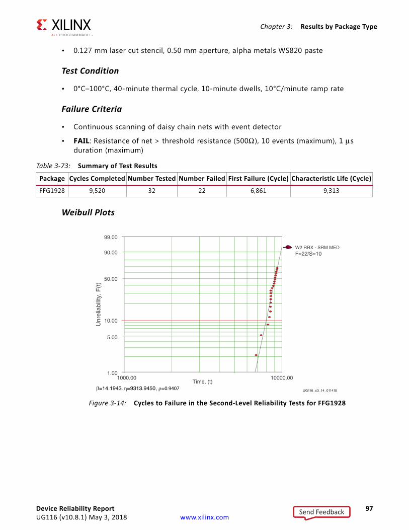
Chapter 3: Results by Package Type
• 0.127 mm laser cut stencil, 0.50 mm aperture, alpha metals WS820 paste
Test Condition
• 0°C–100°C, 40-minute thermal cycle, 10-minute dwells, 10°C/minute ramp rate
Failure Criteria
• Continuous scanning of daisy chain nets with event detector
• FAIL: Resistance of net > threshold resistance (500Ω ), 10 events (maximum), 1 μs duration (maximum)
Weibull Plots
Table 3-73: Summary of Test Results
Package Cycles Completed Number Tested Number Failed First Failure (Cycle) Characteristic Life (Cycle)
FFG1928 9,520 32 22 6,861 9,313
X-Ref Target - Figure 3-14
Figure 3-14: Cycles to Failure in the Second-Level Reliability Tests for FFG1928
UG116_c3_14_011415
1000.00Time, (t)
10000.00
Unr
elia
bilit
y, F
(t)
1.00
5.00
10.00
50.00
90.00
99.00
β=14.1943, η=9313.9450, ρ=0.9407
W2 RRX - SRM MEDF=22/S=10
Device Reliability Report 97UG116 (v10.8.1) May 3, 2018 www.xilinx.com
Send Feedback
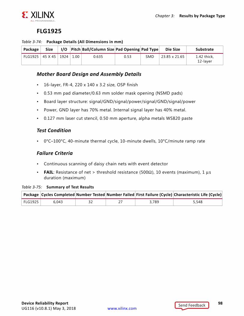
Chapter 3: Results by Package Type
FLG1925
Mother Board Design and Assembly Details
• 16-layer, FR-4, 220 x 140 x 3.2 size, OSP finish
• 0.53 mm pad diameter/0.63 mm solder mask opening (NSMD pads)
• Board layer structure: signal/GND/signal/power/signal/GND/signal/power
• Power, GND layer has 70% metal. Internal signal layer has 40% metal.
• 0.127 mm laser cut stencil, 0.50 mm aperture, alpha metals WS820 paste
Test Condition
• 0°C–100°C, 40-minute thermal cycle, 10-minute dwells, 10°C/minute ramp rate
Failure Criteria
• Continuous scanning of daisy chain nets with event detector
• FAIL: Resistance of net > threshold resistance (500Ω ), 10 events (maximum), 1 μs duration (maximum)
Table 3-74: Package Details (All Dimensions in mm)
Package Size I/O Pitch Ball/Column Size Pad Opening Pad Type Die Size Substrate
FLG1925 45 X 45 1924 1.00 0.635 0.53 SMD 23.85 x 21.65 1.42 thick, 12-layer
Table 3-75: Summary of Test Results
Package Cycles Completed Number Tested Number Failed First Failure (Cycle) Characteristic Life (Cycle)
FLG1925 6,043 32 27 3,789 5,548
Device Reliability Report 98UG116 (v10.8.1) May 3, 2018 www.xilinx.com
Send Feedback
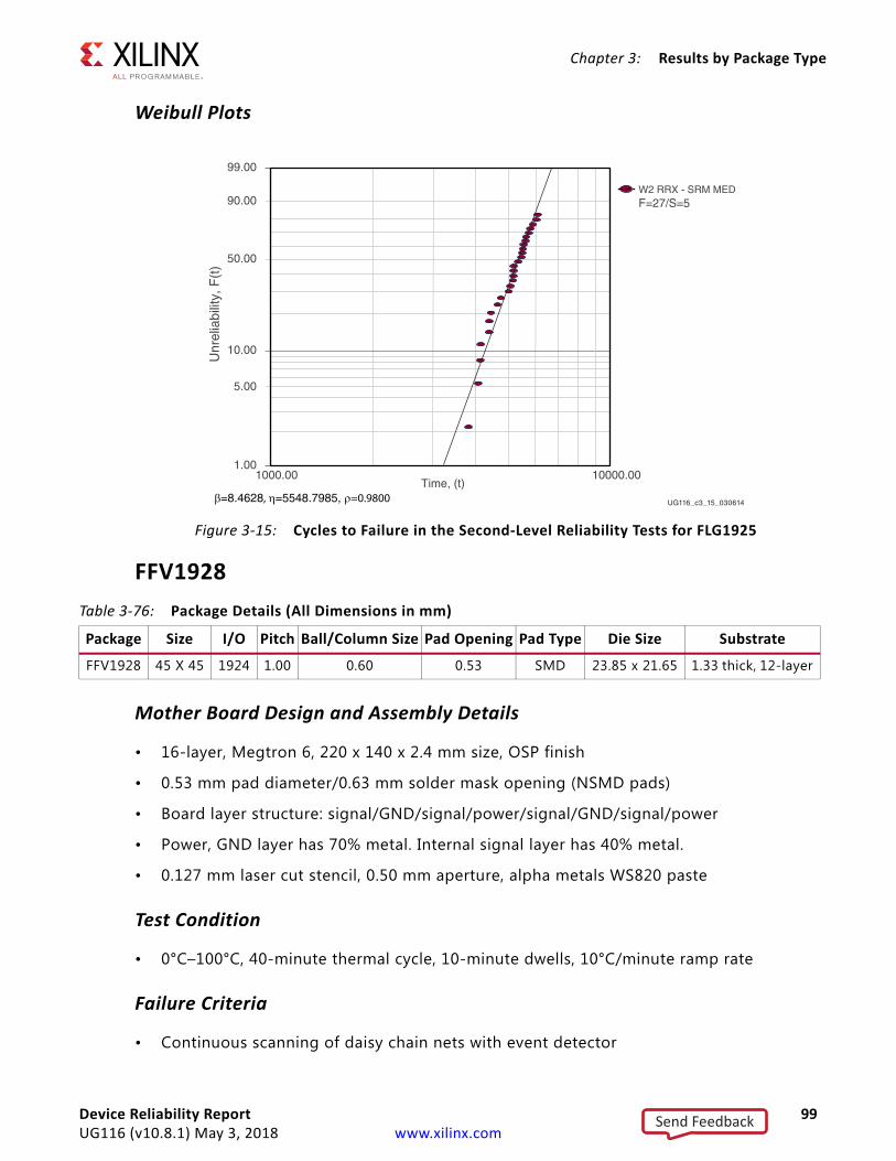
Chapter 3: Results by Package Type
Weibull Plots
FFV1928
Mother Board Design and Assembly Details
• 16-layer, Megtron 6, 220 x 140 x 2.4 mm size, OSP finish
• 0.53 mm pad diameter/0.63 mm solder mask opening (NSMD pads)
• Board layer structure: signal/GND/signal/power/signal/GND/signal/power
• Power, GND layer has 70% metal. Internal signal layer has 40% metal.
• 0.127 mm laser cut stencil, 0.50 mm aperture, alpha metals WS820 paste
Test Condition
• 0°C–100°C, 40-minute thermal cycle, 10-minute dwells, 10°C/minute ramp rate
Failure Criteria
• Continuous scanning of daisy chain nets with event detector
X-Ref Target - Figure 3-15
Figure 3-15: Cycles to Failure in the Second-Level Reliability Tests for FLG1925
UG116_c3_15_030614
1000.00Time, (t)
10000.00
Unr
elia
bilit
y, F
(t)
1.00
5.00
10.00
50.00
90.00
99.00
β=8.4628, η=5548.7985, ρ=0.9800
W2 RRX - SRM MEDF=27/S=5
Table 3-76: Package Details (All Dimensions in mm)
Package Size I/O Pitch Ball/Column Size Pad Opening Pad Type Die Size Substrate
FFV1928 45 X 45 1924 1.00 0.60 0.53 SMD 23.85 x 21.65 1.33 thick, 12-layer
Device Reliability Report 99UG116 (v10.8.1) May 3, 2018 www.xilinx.com
Send Feedback
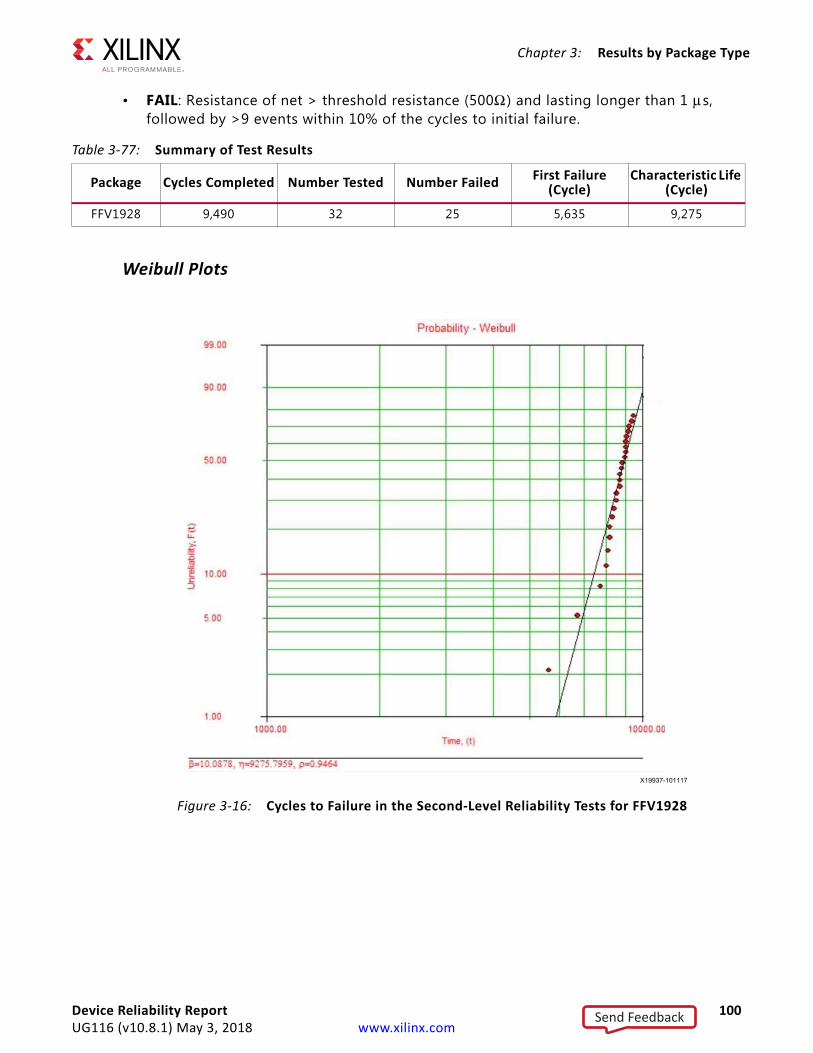
Chapter 3: Results by Package Type
• FAIL: Resistance of net > threshold resistance (500Ω ) and lasting longer than 1 μs, followed by >9 events within 10% of the cycles to initial failure.
Weibull Plots
Table 3-77: Summary of Test Results
Package Cycles Completed Number Tested Number Failed First Failure (Cycle)
Characteristic Life (Cycle)
FFV1928 9,490 32 25 5,635 9,275
X-Ref Target - Figure 3-16
Figure 3-16: Cycles to Failure in the Second-Level Reliability Tests for FFV1928
Device Reliability Report 100UG116 (v10.8.1) May 3, 2018 www.xilinx.com
Send Feedback
Chapter 3: Results by Package Type
FBVA900
Mother Board Design and Assembly Details
• 16-layer, Megtron-6, 290 x 140 x 3.2 mm size, OSP finish
• 0.53 mm pad diameter/0.63 mm solder mask opening (NSMD pads)
• Board layer structure: 16 layer with simulated power, ground (70% metal), and signal (40% metal) layer
• 0.127 mm laser cut stencil, 0.530 mm aperture, Indium 8.9HF paste
Test Condition
• 0°C–100°C, 40-minute thermal cycle, 10-minute dwells, 10°C/minute ramp rate
Failure Criteria
• Continuous scanning of daisy chain nets with event detection
• FAIL: Resistance of net > threshold resistance (500Ω ), 10 events (maximum), 1 μs duration (maximum)
Table 3-78: Package Details (All Dimensions in mm)
Package Size I/O PitchBall/
Column Size
Pad Opening Pad Type Die Size Substrate
FBVA900 31 X 31 900 1.00 0.60 0.53 SMD 16.30 x 11.36 x 0.762 1.24 thick, 10-layer
Table 3-79: Summary of Test Results
Package Cycles Completed Number Tested Number Failed First Failure (Cycle)
Characteristic Life (Cycle)
FBVA900 8737 32 28 7181 8260
Device Reliability Report 101UG116 (v10.8.1) May 3, 2018 www.xilinx.com
Send Feedback
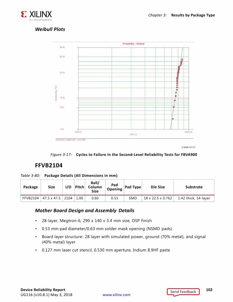
Chapter 3: Results by Package Type
Weibull Plots
FFVB2104
Mother Board Design and Assembly Details
• 28-layer, Megtron-6, 290 x 140 x 3.4 mm size, OSP finish
• 0.53 mm pad diameter/0.63 mm solder mask opening (NSMD pads)
• Board layer structure: 28 layer with simulated power, ground (70% metal), and signal (40% metal) layer
• 0.127 mm laser cut stencil, 0.530 mm aperture, Indium 8.9HF paste
X-Ref Target - Figure 3-17
Figure 3-17: Cycles to Failure in the Second-Level Reliability Tests for FBVA900
Table 3-80: Package Details (All Dimensions in mm)
Package Size I/O PitchBall/
Column Size
Pad Opening Pad Type Die Size Substrate
FFVB2104 47.5 x 47.5 2104 1.00 0.60 0.53 SMD 18 x 22.5 x 0.762 1.42 thick, 14-layer
Device Reliability Report 102UG116 (v10.8.1) May 3, 2018 www.xilinx.com
Send Feedback
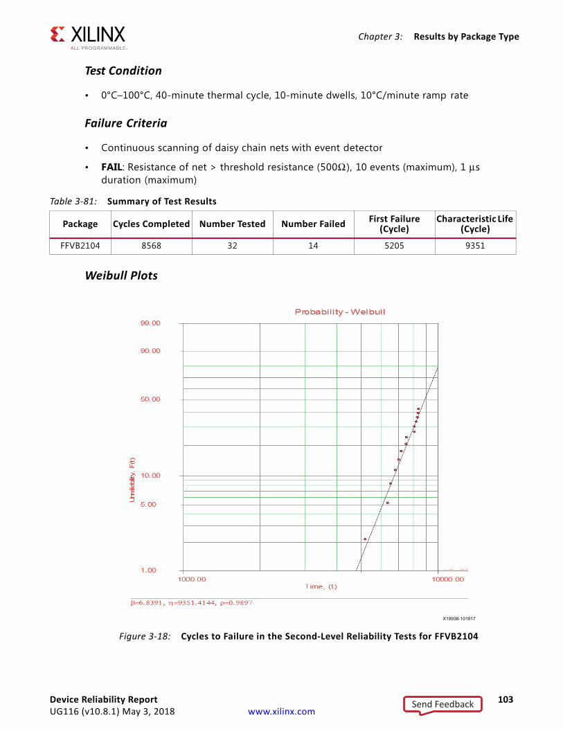
Chapter 3: Results by Package Type
Test Condition
• 0°C–100°C, 40-minute thermal cycle, 10-minute dwells, 10°C/minute ramp rate
Failure Criteria
• Continuous scanning of daisy chain nets with event detector
• FAIL: Resistance of net > threshold resistance (500Ω ), 10 events (maximum), 1 μs duration (maximum)
Weibull Plots
Table 3-81: Summary of Test Results
Package Cycles Completed Number Tested Number Failed First Failure (Cycle)
Characteristic Life (Cycle)
FFVB2104 8568 32 14 5205 9351
X-Ref Target - Figure 3-18
Figure 3-18: Cycles to Failure in the Second-Level Reliability Tests for FFVB2104
Device Reliability Report 103UG116 (v10.8.1) May 3, 2018 www.xilinx.com
Send Feedback
Chapter 3: Results by Package Type
FLVA1924
Mother Board Design and Assembly Details
• 28-layer, Megtron-6, 290 x 140 x 3.4 mm size, OSP finish
• 0.53 mm pad diameter/0.63 mm solder mask opening (NSMD pads)
• Board layer structure: 28 layer with simulated power, ground (70% metal), and signal (40% metal) layer
• 0.127 mm laser cut stencil, 0.530 mm aperture, Indium 8.9HF paste
Test Condition
• 0°C–100°C, 40-minute thermal cycle, 10-minute dwells, 10°C/minute ramp rate
Failure Criteria
• Continuous scanning of daisy chain nets with event detector
• FAIL: Resistance of net > threshold resistance (500Ω ), 10 events (maximum), 1 μs duration (maximum)
Table 3-82: Package Details (All Dimensions in mm)
Package Size I/O PitchBall/
Column Size
Pad Opening
Pad Type Die Size Substrate
FLVA1924 45 x 45 1924 1.00 0.60 0.53 SMD 14.4 x 23 x 0.10 (2 pcs)
25 x 31 x 0.50
2.00 thick, 18-layer
Table 3-83: Summary of Test Results
Package Cycles Completed Number Tested Number Failed First Failure (Cycle)
Characteristic Life (Cycle)
FLVA1924 4605 32 25 2759 4222
Device Reliability Report 104UG116 (v10.8.1) May 3, 2018 www.xilinx.com
Send Feedback
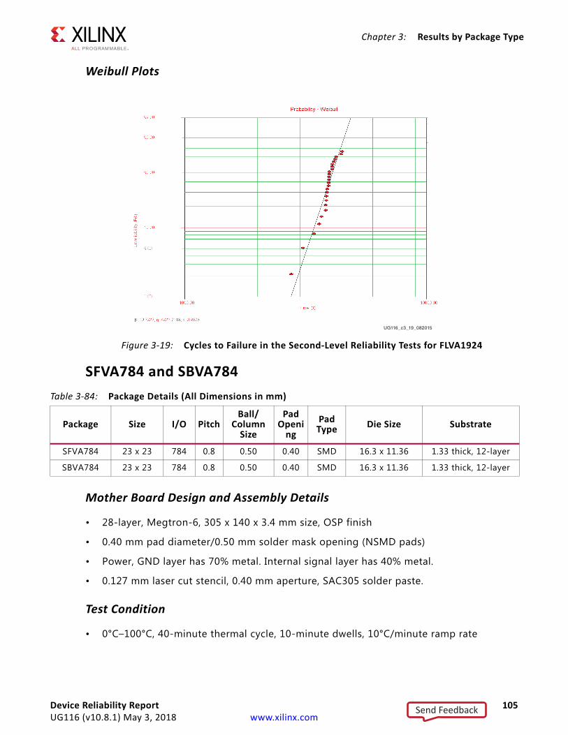
Chapter 3: Results by Package Type
Weibull Plots
SFVA784 and SBVA784
Mother Board Design and Assembly Details
• 28-layer, Megtron-6, 305 x 140 x 3.4 mm size, OSP finish
• 0.40 mm pad diameter/0.50 mm solder mask opening (NSMD pads)
• Power, GND layer has 70% metal. Internal signal layer has 40% metal.
• 0.127 mm laser cut stencil, 0.40 mm aperture, SAC305 solder paste.
Test Condition
• 0°C–100°C, 40-minute thermal cycle, 10-minute dwells, 10°C/minute ramp rate
X-Ref Target - Figure 3-19
Figure 3-19: Cycles to Failure in the Second-Level Reliability Tests for FLVA1924
UG116_c3_19_082015
Table 3-84: Package Details (All Dimensions in mm)
Package Size I/O PitchBall/
Column Size
Pad Openi
ngPad
Type Die Size Substrate
SFVA784 23 x 23 784 0.8 0.50 0.40 SMD 16.3 x 11.36 1.33 thick, 12-layer
SBVA784 23 x 23 784 0.8 0.50 0.40 SMD 16.3 x 11.36 1.33 thick, 12-layer
Device Reliability Report 105UG116 (v10.8.1) May 3, 2018 www.xilinx.com
Send Feedback
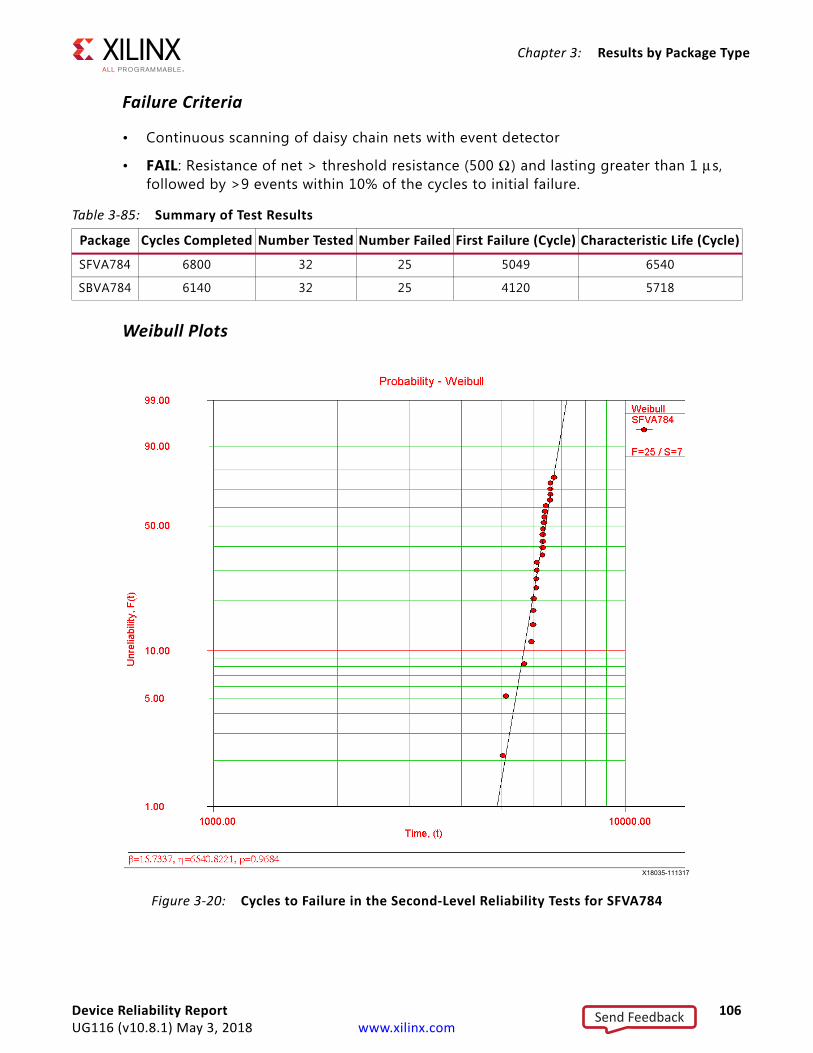
Chapter 3: Results by Package Type
Failure Criteria
• Continuous scanning of daisy chain nets with event detector
• FAIL: Resistance of net > threshold resistance (500 Ω ) and lasting greater than 1 μs, followed by >9 events within 10% of the cycles to initial failure.
Weibull Plots
Table 3-85: Summary of Test Results
Package Cycles Completed Number Tested Number Failed First Failure (Cycle) Characteristic Life (Cycle)
SFVA784 6800 32 25 5049 6540
SBVA784 6140 32 25 4120 5718
X-Ref Target - Figure 3-20
Figure 3-20: Cycles to Failure in the Second-Level Reliability Tests for SFVA784
Device Reliability Report 106UG116 (v10.8.1) May 3, 2018 www.xilinx.com
Send Feedback
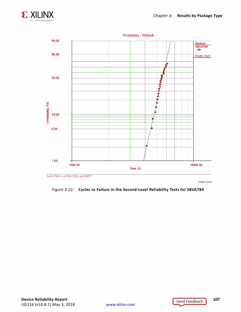
Chapter 3: Results by Package Type
X-Ref Target - Figure 3-21
Figure 3-21: Cycles to Failure in the Second-Level Reliability Tests for SBVA784
X19945-101817
Device Reliability Report 107UG116 (v10.8.1) May 3, 2018 www.xilinx.com
Send Feedback
Appendix A
Additional Resources and Legal Notices
Xilinx ResourcesFor support resources such as Answers, Documentation, Downloads, and Forums, see Xilinx Support.
Solution CentersSee the Xilinx Solution Centers for support on devices, software tools, and intellectual property at all stages of the design cycle. Topics include design assistance, advisories, and troubleshooting tips.
Documentation Navigator and Design HubsXilinx® Documentation Navigator provides access to Xilinx documents, videos, and support resources, which you can filter and search to find information. To open the Xilinx Documentation Navigator (DocNav):
• From the Vivado® IDE, select Help > Documentation and Tutorials.
• On Windows, select Start > All Programs > Xilinx Design Tools > DocNav.
• At the Linux command prompt, enter docnav.
Xilinx Design Hubs provide links to documentation organized by design tasks and other topics, which you can use to learn key concepts and address frequently asked questions. To access the Design Hubs:
• In the Xilinx Documentation Navigator, click the Design Hubs View tab.
• On the Xilinx website, see the Design Hubs page.
Note: For more information on Documentation Navigator, see the Documentation Navigator page on the Xilinx website.
Device Reliability Report 108UG116 (v10.8.1) May 3, 2018 www.xilinx.com
Send Feedback
Appendix A: Additional Resources and Legal Notices
References1. Device Package User Guide (UG112)
2. Continuing Experiments of Atmospheric Neutron Effects on Deep Submicron Integrated Circuits (WP286)
3. Virtex-4 FPGA Packaging and Pinout Specification (UG075)
4. Virtex-5 FPGA Packaging and Pinout Specification (UG195)
5. Virtex-6 FPGA Packaging and Pinout Specifications (UG365)
6. Spartan-6 FPGA Packaging and Pinouts Product Specification (UG385)
7. 7 Series FPGAs Packaging and Pinout Product Specification (UG475)
8. Zynq-7000 All Programmable SoC Packaging and Pinout Product Specification (UG865)
9. UltraScale and UltraScale+ FPGAs Packaging and Pinouts Product Specification (UG575)
10. Zynq UltraScale+ MPSoC Packaging and Pinouts Product Specification User Guide (UG1075)
Please Read: Important Legal NoticesThe information disclosed to you hereunder (the “Materials”) is provided solely for the selection and use of Xilinx products. To the maximum extent permitted by applicable law: (1) Materials are made available "AS IS" and with all faults, Xilinx hereby DISCLAIMS ALL WARRANTIES AND CONDITIONS, EXPRESS, IMPLIED, OR STATUTORY, INCLUDING BUT NOT LIMITED TO WARRANTIES OF MERCHANTABILITY, NON-INFRINGEMENT, OR FITNESS FOR ANY PARTICULAR PURPOSE; and (2) Xilinx shall not be liable (whether in contract or tort, including negligence, or under any other theory of liability) for any loss or damage of any kind or nature related to, arising under, or in connection with, the Materials (including your use of the Materials), including for any direct, indirect, special, incidental, or consequential loss or damage (including loss of data, profits, goodwill, or any type of loss or damage suffered as a result of any action brought by a third party) even if such damage or loss was reasonably foreseeable or Xilinx had been advised of the possibility of the same. Xilinx assumes no obligation to correct any errors contained in the Materials or to notify you of updates to the Materials or to product specifications. You may not reproduce, modify, distribute, or publicly display the Materials without prior written consent. Certain products are subject to the terms and conditions of Xilinx’s limited warranty, please refer to Xilinx’s Terms of Sale which can be viewed at https://www.xilinx.com/legal.htm#tos; IP cores may be subject to warranty and support terms contained in a license issued to you by Xilinx. Xilinx products are not designed or intended to be fail-safe or for use in any application requiring fail-safe performance; you assume sole risk and liability for use of Xilinx products in such critical applications, please refer to Xilinx’s Terms of Sale which can be viewed at https://www.xilinx.com/legal.htm#tos.AUTOMOTIVE APPLICATIONS DISCLAIMERAUTOMOTIVE PRODUCTS (IDENTIFIED AS “XA” IN THE PART NUMBER) ARE NOT WARRANTED FOR USE IN THE DEPLOYMENT OF AIRBAGS OR FOR USE IN APPLICATIONS THAT AFFECT CONTROL OF A VEHICLE (“SAFETY APPLICATION”) UNLESS THERE IS A SAFETY CONCEPT OR REDUNDANCY FEATURE CONSISTENT WITH THE ISO 26262 AUTOMOTIVE SAFETY STANDARD (“SAFETY DESIGN”). CUSTOMER SHALL, PRIOR TO USING OR DISTRIBUTING ANY SYSTEMS THAT INCORPORATE PRODUCTS, THOROUGHLY TEST SUCH SYSTEMS FOR SAFETY PURPOSES. USE OF PRODUCTS IN A SAFETY APPLICATION WITHOUT A SAFETY DESIGN IS FULLY AT THE RISK OF CUSTOMER, SUBJECT ONLY TO APPLICABLE LAWS AND REGULATIONS GOVERNING LIMITATIONS ON PRODUCT LIABILITY.© Copyright 2014–2018 Xilinx, Inc. Xilinx, the Xilinx logo, Artix, ISE, Kintex, Spartan, Virtex, Vivado, Zynq, and other designated brands included herein are trademarks of Xilinx in the United States and other countries. All other trademarks are the property of their respective owners.
Device Reliability Report 109UG116 (v10.8.1) May 3, 2018 www.xilinx.com
Send Feedback