Embed Size (px)
Citation preview
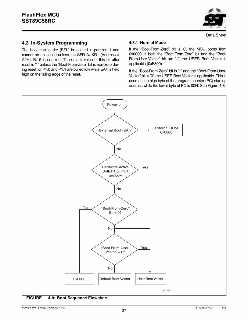
Data Sheet
FEATURES:
• 8-bit 8051-Compatible Microcontroller (MCU) with Embedded SuperFlash Memory– Fully Software Compatible– Development Toolset Compatible– Pin-for-Pin Package Compatible
• SST89C58RC Operation– 0 to 40 MHz at 2.7-5.5V
• 34 KByte Single Block SuperFlash EEPROMwith two partitions– 32 KByte primary partition + 2 KByte secondary
partition– Flash Block is divided into four application
pages (8 KByte) and one loader page (2 KByte)– Individual Page Security Lock– Address up to 64KB for External Data Memory– In-System Programming (ISP)– In-Application Programming (IAP)– Small-Sector Architecture: 128-Byte Sector Size
• Total 1KByte On-chip RAM• Supports External Address Range up to 64
KByte of Program and Data Memory• Dual Enhanced SMBus
– Up to 400 Kbit per second• Full-Duplex, Enhanced UART
– Framing error detection– Automatic address recognition
• Brown-out Reset (BOR)• Nine Interrupt Sources at 4 Priority Levels• Three 16-bit Timers/Counters• Programmable Watchdog Timer (WDT)• Second DPTR register• Four 8-bit I/O Ports (32 I/O pins) • I/O pins can tolerate VDD +0.5V (Pulled up and
driven to 5.5V)• Standard 12 Clocks per cycle, the device has an
option to double the speed to 6 clocks per cycle– Speeds up to 40 MHz with 12 clock cycles per
machine cycle– Speeds up to 20 MHz with 6 clock cycles per
machine cycle - equivalent to 40 MHz• Enhanced Hook Emulation• Low Power Modes
– Power-down Mode with External Interrupt Wake-up – Idle Mode
• Temperature Ranges:– Industrial (-40°C to +85°C)– Commercial (0°C to +70°C)
• Packages Available– 44-lead PLCC– 44-lead TQFP– 40-contact WQFN
• All non-Pb (lead-free) devices are RoHS compliant
FlashFlex MCUSST89C58RC
SST89E/VE5xC FlashFlex51 MCU
PRODUCT DESCRIPTION
The SST89C58RC is a member of the FlashFlex family of8-bit micro controllers designed and manufactured withSST patented and proprietary SuperFlash CMOS semi-conductor process technology. The split-gate cell designand thick-oxide tunneling injector offer significant cost andreliability benefits for customers. It uses the 8051 instruc-tion set and is pin-for-pin compatible with standard 8051micro controller devices.
With two enhanced SMBus interfaces, the SST89C58RCsupports speeds up to 400 Kbps. It comes with 34 KByte ofon-chip flash EEPROM program memory which is dividedinto two independent program memory partitions. The pri-mary partition occupies 32 KByte of internal program mem-ory space and the secondary partition occupies 2 KByte ofinternal program memory space.
The flash memory can be programmed via a standard87C5x OTP EPROM programmer fitted with a specialadapter and firmware for SST devices. The SST89C58RCis designed to be programmed in-system on the printed cir-
cuit board for maximum flexibility. It is pre-programmed withan example of the bootstrap loader in memory, demonstrat-ing initial user program code loading or subsequent usercode updating via an ISP operation. The sample bootstraploader is for the user’s reference only, and SST does notguarantee its functionality. Chip-Erase operations will erasethe pre-programmed sample code.
In addition to 34 KByte of SuperFlash EEPROM on-chipprogram memory and 1024 x8 bits of on-chip RAM, thedevice can address up to 64 KByte of external programmemory and up to 64 KByte of external RAM.
The highly-reliable, patented SST SuperFlash technologyand memory cell architecture offer a number of importantadvantages for designing and manufacturing flashEEPROMs. These advantages translate into significantcost and reliability benefits for customers.
©2008 Silicon Storage Technology, Inc.S71323-05-000 12/081
The SST logo, SuperFlash, and FlashFlex are registered trademarks of Silicon Storage Technology, Inc.These specifications are subject to change without notice.
Data Sheet
FlashFlex MCUSST89C58RC
TABLE OF CONTENTS
FEATURES:. . . . . . . . . . . . . . . . . . . . . . . . . . . . . . . . . . . . . . . . . . . . . . . . . . . . . . . . . . . . . . . . . . . . . . . . . . . . . . . 1
PRODUCT DESCRIPTION . . . . . . . . . . . . . . . . . . . . . . . . . . . . . . . . . . . . . . . . . . . . . . . . . . . . . . . . . . . . . . . . . . . 1
TABLE OF CONTENTS. . . . . . . . . . . . . . . . . . . . . . . . . . . . . . . . . . . . . . . . . . . . . . . . . . . . . . . . . . . . . . . . . . . . . . 2
LIST OF FIGURES . . . . . . . . . . . . . . . . . . . . . . . . . . . . . . . . . . . . . . . . . . . . . . . . . . . . . . . . . . . . . . . . . . . . . . . . . 4
LIST OF TABLES. . . . . . . . . . . . . . . . . . . . . . . . . . . . . . . . . . . . . . . . . . . . . . . . . . . . . . . . . . . . . . . . . . . . . . . . . . . 5
1.0 FUNCTIONAL BLOCKS . . . . . . . . . . . . . . . . . . . . . . . . . . . . . . . . . . . . . . . . . . . . . . . . . . . . . . . . . . . . . . . . . 6
2.0 PIN ASSIGNMENTS. . . . . . . . . . . . . . . . . . . . . . . . . . . . . . . . . . . . . . . . . . . . . . . . . . . . . . . . . . . . . . . . . . . . 7
2.1 Pin Descriptions . . . . . . . . . . . . . . . . . . . . . . . . . . . . . . . . . . . . . . . . . . . . . . . . . . . . . . . . . . . . . . . . . . . . 9
2.2 I/O Descriptions . . . . . . . . . . . . . . . . . . . . . . . . . . . . . . . . . . . . . . . . . . . . . . . . . . . . . . . . . . . . . . . . . . . 10
3.0 MEMORY ORGANIZATION . . . . . . . . . . . . . . . . . . . . . . . . . . . . . . . . . . . . . . . . . . . . . . . . . . . . . . . . . . . . . 11
3.1 Program Flash Memory . . . . . . . . . . . . . . . . . . . . . . . . . . . . . . . . . . . . . . . . . . . . . . . . . . . . . . . . . . . . . 11
3.2 Data RAM Memory. . . . . . . . . . . . . . . . . . . . . . . . . . . . . . . . . . . . . . . . . . . . . . . . . . . . . . . . . . . . . . . . . 12
3.3 Expanded Data RAM Addressing . . . . . . . . . . . . . . . . . . . . . . . . . . . . . . . . . . . . . . . . . . . . . . . . . . . . . 12
3.4 Dual Data Pointers . . . . . . . . . . . . . . . . . . . . . . . . . . . . . . . . . . . . . . . . . . . . . . . . . . . . . . . . . . . . . . . . . 14
3.5 Special Function Registers . . . . . . . . . . . . . . . . . . . . . . . . . . . . . . . . . . . . . . . . . . . . . . . . . . . . . . . . . . 14
4.0 FLASH MEMORY PROGRAMMING . . . . . . . . . . . . . . . . . . . . . . . . . . . . . . . . . . . . . . . . . . . . . . . . . . . . . . 33
4.1 Product Identification . . . . . . . . . . . . . . . . . . . . . . . . . . . . . . . . . . . . . . . . . . . . . . . . . . . . . . . . . . . . . . . 33
4.2 In-Application Programming. . . . . . . . . . . . . . . . . . . . . . . . . . . . . . . . . . . . . . . . . . . . . . . . . . . . . . . . . . 33
4.3 In-System Programming . . . . . . . . . . . . . . . . . . . . . . . . . . . . . . . . . . . . . . . . . . . . . . . . . . . . . . . . . . . . 37
5.0 TIMERS/COUNTERS . . . . . . . . . . . . . . . . . . . . . . . . . . . . . . . . . . . . . . . . . . . . . . . . . . . . . . . . . . . . . . . . . . 39
5.1 Timers . . . . . . . . . . . . . . . . . . . . . . . . . . . . . . . . . . . . . . . . . . . . . . . . . . . . . . . . . . . . . . . . . . . . . . . . . . 39
5.2 Timer Set-up . . . . . . . . . . . . . . . . . . . . . . . . . . . . . . . . . . . . . . . . . . . . . . . . . . . . . . . . . . . . . . . . . . . . . 39
5.3 Programmable Clock-Out. . . . . . . . . . . . . . . . . . . . . . . . . . . . . . . . . . . . . . . . . . . . . . . . . . . . . . . . . . . . 40
6.0 SERIAL I/O . . . . . . . . . . . . . . . . . . . . . . . . . . . . . . . . . . . . . . . . . . . . . . . . . . . . . . . . . . . . . . . . . . . . . . . . . . 40
6.1 Full-Duplex, Enhanced UART . . . . . . . . . . . . . . . . . . . . . . . . . . . . . . . . . . . . . . . . . . . . . . . . . . . . . . . . 40
6.2 Enhanced SMBus Interface . . . . . . . . . . . . . . . . . . . . . . . . . . . . . . . . . . . . . . . . . . . . . . . . . . . . . . . . . . 44
6.3 Timeouts . . . . . . . . . . . . . . . . . . . . . . . . . . . . . . . . . . . . . . . . . . . . . . . . . . . . . . . . . . . . . . . . . . . . . . . . 45
6.4 SMBus SFR . . . . . . . . . . . . . . . . . . . . . . . . . . . . . . . . . . . . . . . . . . . . . . . . . . . . . . . . . . . . . . . . . . . . . . 46
7.0 WATCHDOG TIMER . . . . . . . . . . . . . . . . . . . . . . . . . . . . . . . . . . . . . . . . . . . . . . . . . . . . . . . . . . . . . . . . . . 56
7.1 Watchdog Timer Mode. . . . . . . . . . . . . . . . . . . . . . . . . . . . . . . . . . . . . . . . . . . . . . . . . . . . . . . . . . . . . . 56
7.2 Pure Timer Mode . . . . . . . . . . . . . . . . . . . . . . . . . . . . . . . . . . . . . . . . . . . . . . . . . . . . . . . . . . . . . . . . . . 56
7.3 Clock Source . . . . . . . . . . . . . . . . . . . . . . . . . . . . . . . . . . . . . . . . . . . . . . . . . . . . . . . . . . . . . . . . . . . . . 56
7.4 Feed Sequence . . . . . . . . . . . . . . . . . . . . . . . . . . . . . . . . . . . . . . . . . . . . . . . . . . . . . . . . . . . . . . . . . . . 56
7.5 Power Saving Considerations for Using the Watchdog Timer . . . . . . . . . . . . . . . . . . . . . . . . . . . . . . . . 56
8.0 SECURITY LOCK. . . . . . . . . . . . . . . . . . . . . . . . . . . . . . . . . . . . . . . . . . . . . . . . . . . . . . . . . . . . . . . . . . . . . 58
8.1 Chip-Level Security Lock . . . . . . . . . . . . . . . . . . . . . . . . . . . . . . . . . . . . . . . . . . . . . . . . . . . . . . . . . . . . 58
8.2 Page-Level Security Lock . . . . . . . . . . . . . . . . . . . . . . . . . . . . . . . . . . . . . . . . . . . . . . . . . . . . . . . . . . . 58
8.3 Read Operation Under Lock Condition . . . . . . . . . . . . . . . . . . . . . . . . . . . . . . . . . . . . . . . . . . . . . . . . . 58
9.0 RESET . . . . . . . . . . . . . . . . . . . . . . . . . . . . . . . . . . . . . . . . . . . . . . . . . . . . . . . . . . . . . . . . . . . . . . . . . . . . . 59
9.1 Power-on Reset . . . . . . . . . . . . . . . . . . . . . . . . . . . . . . . . . . . . . . . . . . . . . . . . . . . . . . . . . . . . . . . . . . . 59
9.2 Interrupt Priority and Polling Sequence . . . . . . . . . . . . . . . . . . . . . . . . . . . . . . . . . . . . . . . . . . . . . . . . . 59
2©2008 Silicon Storage Technology, Inc. S71323-05-000 12/08
Data Sheet
FlashFlex MCUSST89C58RC
10.0 POWER-SAVING MODES . . . . . . . . . . . . . . . . . . . . . . . . . . . . . . . . . . . . . . . . . . . . . . . . . . . . . . . . . . . . . . 62
10.1 Idle Mode . . . . . . . . . . . . . . . . . . . . . . . . . . . . . . . . . . . . . . . . . . . . . . . . . . . . . . . . . . . . . . . . . . . . . . . 62
10.2 Power-down Mode . . . . . . . . . . . . . . . . . . . . . . . . . . . . . . . . . . . . . . . . . . . . . . . . . . . . . . . . . . . . . . . . 62
11.0 SYSTEM CLOCK AND CLOCK OPTIONS. . . . . . . . . . . . . . . . . . . . . . . . . . . . . . . . . . . . . . . . . . . . . . . . . . 63
11.1 Clock Input Options and Recommended Capacitor Values for Oscillator . . . . . . . . . . . . . . . . . . . . . . 63
11.2 Clock Doubling Option . . . . . . . . . . . . . . . . . . . . . . . . . . . . . . . . . . . . . . . . . . . . . . . . . . . . . . . . . . . . . 63
12.0 ELECTRICAL SPECIFICATION . . . . . . . . . . . . . . . . . . . . . . . . . . . . . . . . . . . . . . . . . . . . . . . . . . . . . . . . . . 64
12.1 DC Electrical Characteristics . . . . . . . . . . . . . . . . . . . . . . . . . . . . . . . . . . . . . . . . . . . . . . . . . . . . . . . . 66
12.2 AC Electrical Characteristics . . . . . . . . . . . . . . . . . . . . . . . . . . . . . . . . . . . . . . . . . . . . . . . . . . . . . . . . 67
13.0 PRODUCT ORDERING INFORMATION . . . . . . . . . . . . . . . . . . . . . . . . . . . . . . . . . . . . . . . . . . . . . . . . . . . 73
13.1 Valid Combinations . . . . . . . . . . . . . . . . . . . . . . . . . . . . . . . . . . . . . . . . . . . . . . . . . . . . . . . . . . . . . . . 73
14.0 PACKAGING DIAGRAMS . . . . . . . . . . . . . . . . . . . . . . . . . . . . . . . . . . . . . . . . . . . . . . . . . . . . . . . . . . . . . . 74
3©2008 Silicon Storage Technology, Inc. S71323-05-000 12/08
Data Sheet
FlashFlex MCUSST89C58RC
LIST OF FIGURES
FIGURE 1-1: Functional Block Diagram. . . . . . . . . . . . . . . . . . . . . . . . . . . . . . . . . . . . . . . . . . . . . . . . . . . . . 6
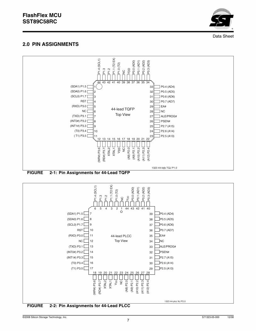
FIGURE 2-1: Pin Assignments for 44-Lead TQFP. . . . . . . . . . . . . . . . . . . . . . . . . . . . . . . . . . . . . . . . . . . . . 7
FIGURE 2-2: Pin Assignments for 44-Lead PLCC. . . . . . . . . . . . . . . . . . . . . . . . . . . . . . . . . . . . . . . . . . . . . 7
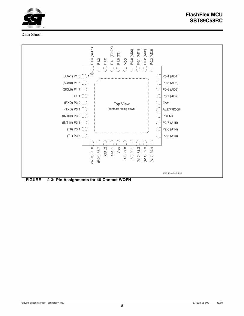
FIGURE 2-3: Pin Assignments for 40-Contact WQFN . . . . . . . . . . . . . . . . . . . . . . . . . . . . . . . . . . . . . . . . . . 8
FIGURE 3-1: Program Memory Organization. . . . . . . . . . . . . . . . . . . . . . . . . . . . . . . . . . . . . . . . . . . . . . . . 11
FIGURE 3-2: Internal and External Data Memory Structure . . . . . . . . . . . . . . . . . . . . . . . . . . . . . . . . . . . . 13
FIGURE 3-3: Dual Data Pointer Organization . . . . . . . . . . . . . . . . . . . . . . . . . . . . . . . . . . . . . . . . . . . . . . . 14
FIGURE 4-1: Chip-Erase . . . . . . . . . . . . . . . . . . . . . . . . . . . . . . . . . . . . . . . . . . . . . . . . . . . . . . . . . . . . . . . 34
FIGURE 4-2: Partition0-Erase . . . . . . . . . . . . . . . . . . . . . . . . . . . . . . . . . . . . . . . . . . . . . . . . . . . . . . . . . . . 35
FIGURE 4-3: Sector-Erase. . . . . . . . . . . . . . . . . . . . . . . . . . . . . . . . . . . . . . . . . . . . . . . . . . . . . . . . . . . . . . 35
FIGURE 4-4: Byte-Program . . . . . . . . . . . . . . . . . . . . . . . . . . . . . . . . . . . . . . . . . . . . . . . . . . . . . . . . . . . . . 35
FIGURE 4-5: Byte-Verify . . . . . . . . . . . . . . . . . . . . . . . . . . . . . . . . . . . . . . . . . . . . . . . . . . . . . . . . . . . . . . . 35
FIGURE 4-6: Secure-Page0-4 . . . . . . . . . . . . . . . . . . . . . . . . . . . . . . . . . . . . . . . . . . . . . . . . . . . . . . . . . . . 36
FIGURE 4-7: Enable-Clock-Double . . . . . . . . . . . . . . . . . . . . . . . . . . . . . . . . . . . . . . . . . . . . . . . . . . . . . . . 36
FIGURE 4-8: Boot Sequence Flowchart. . . . . . . . . . . . . . . . . . . . . . . . . . . . . . . . . . . . . . . . . . . . . . . . . . . . 37
FIGURE 4-9: Hardware Enter Mode. . . . . . . . . . . . . . . . . . . . . . . . . . . . . . . . . . . . . . . . . . . . . . . . . . . . . . . 38
FIGURE 6-1: Framing Error Block Diagram . . . . . . . . . . . . . . . . . . . . . . . . . . . . . . . . . . . . . . . . . . . . . . . . . 41
FIGURE 6-2: UART Timings in Mode 1 . . . . . . . . . . . . . . . . . . . . . . . . . . . . . . . . . . . . . . . . . . . . . . . . . . . . 41
FIGURE 6-3: UART Timings in Modes 2 and 3 . . . . . . . . . . . . . . . . . . . . . . . . . . . . . . . . . . . . . . . . . . . . . . 41
FIGURE 6-4: Typical SMBus Configuration . . . . . . . . . . . . . . . . . . . . . . . . . . . . . . . . . . . . . . . . . . . . . . . . . 44
FIGURE 6-5: Data Transfer on the SUBus. . . . . . . . . . . . . . . . . . . . . . . . . . . . . . . . . . . . . . . . . . . . . . . . . . 44
FIGURE 6-6: SMBus Serial Interface Block Diagram. . . . . . . . . . . . . . . . . . . . . . . . . . . . . . . . . . . . . . . . . . 54
FIGURE 7-1: Block Diagram of Programmable Watchdog Timer . . . . . . . . . . . . . . . . . . . . . . . . . . . . . . . . 57
FIGURE 9-1: Power-on Reset Circuit. . . . . . . . . . . . . . . . . . . . . . . . . . . . . . . . . . . . . . . . . . . . . . . . . . . . . . 59
FIGURE 9-2: Interrupt Sequence . . . . . . . . . . . . . . . . . . . . . . . . . . . . . . . . . . . . . . . . . . . . . . . . . . . . . . . . . 60
FIGURE 11-1: Oscillator Characteristics . . . . . . . . . . . . . . . . . . . . . . . . . . . . . . . . . . . . . . . . . . . . . . . . . . . 63
FIGURE 12-1: External Program Memory Read Cycle . . . . . . . . . . . . . . . . . . . . . . . . . . . . . . . . . . . . . . . . 69
FIGURE 12-2: External Data Memory Read Cycle . . . . . . . . . . . . . . . . . . . . . . . . . . . . . . . . . . . . . . . . . . . 69
FIGURE 12-3: External Data Memory Write Cycle. . . . . . . . . . . . . . . . . . . . . . . . . . . . . . . . . . . . . . . . . . . . 70
FIGURE 12-4: Shift Register Mode Timing Waveforms . . . . . . . . . . . . . . . . . . . . . . . . . . . . . . . . . . . . . . . . 70
FIGURE 12-5: AC Testing Input/Output Test Waveform . . . . . . . . . . . . . . . . . . . . . . . . . . . . . . . . . . . . . . . 71
FIGURE 12-6: Float Waveform . . . . . . . . . . . . . . . . . . . . . . . . . . . . . . . . . . . . . . . . . . . . . . . . . . . . . . . . . . 71
FIGURE 12-7: A Test Load Example . . . . . . . . . . . . . . . . . . . . . . . . . . . . . . . . . . . . . . . . . . . . . . . . . . . . . . 71
FIGURE 12-8: IDD Test Condition, Active Mode. . . . . . . . . . . . . . . . . . . . . . . . . . . . . . . . . . . . . . . . . . . . . . 71
FIGURE 12-9: IDD Test Condition, Idle Mode. . . . . . . . . . . . . . . . . . . . . . . . . . . . . . . . . . . . . . . . . . . . . . . . 72
FIGURE 12-10: IDD Test Condition, Power-down Mode. . . . . . . . . . . . . . . . . . . . . . . . . . . . . . . . . . . . . . . . 72
FIGURE 14-1: 44-lead Plastic Lead Chip Carrier (PLCC) . . . . . . . . . . . . . . . . . . . . . . . . . . . . . . . . . . . . . . 74
FIGURE 14-2: 44-lead Thin Quad Flat Pack (TQFP) . . . . . . . . . . . . . . . . . . . . . . . . . . . . . . . . . . . . . . . . . . 75
FIGURE 14-3: 40-Contact Very-Very-Thin Quad Flat No-lead (WQFN) . . . . . . . . . . . . . . . . . . . . . . . . . . . 76
4©2008 Silicon Storage Technology, Inc. S71323-05-000 12/08
Data Sheet
FlashFlex MCUSST89C58RC
LIST OF TABLES
TABLE 2-1: Pin Descriptions . . . . . . . . . . . . . . . . . . . . . . . . . . . . . . . . . . . . . . . . . . . . . . . . . . . . . . . . . . . . 9
TABLE 3-1: External Data Memory RD#, WR# with EXTRAM bit . . . . . . . . . . . . . . . . . . . . . . . . . . . . . . . 13
TABLE 3-2: FlashFlex SFR Memory Map . . . . . . . . . . . . . . . . . . . . . . . . . . . . . . . . . . . . . . . . . . . . . . . . . 15
TABLE 3-3: CPU related SFRs . . . . . . . . . . . . . . . . . . . . . . . . . . . . . . . . . . . . . . . . . . . . . . . . . . . . . . . . . 15
TABLE 3-4: Flash Memory Programming SFRs . . . . . . . . . . . . . . . . . . . . . . . . . . . . . . . . . . . . . . . . . . . . 16
TABLE 3-5: Watchdog Timer SFRs . . . . . . . . . . . . . . . . . . . . . . . . . . . . . . . . . . . . . . . . . . . . . . . . . . . . . . 16
TABLE 3-6: Timer/Counter SFR. . . . . . . . . . . . . . . . . . . . . . . . . . . . . . . . . . . . . . . . . . . . . . . . . . . . . . . . . 17
TABLE 3-7: Interface SFRs . . . . . . . . . . . . . . . . . . . . . . . . . . . . . . . . . . . . . . . . . . . . . . . . . . . . . . . . . . . . 18
TABLE 3-8: Feed Sequence SFRs . . . . . . . . . . . . . . . . . . . . . . . . . . . . . . . . . . . . . . . . . . . . . . . . . . . . . . 18
TABLE 3-9: Clock Option SFR. . . . . . . . . . . . . . . . . . . . . . . . . . . . . . . . . . . . . . . . . . . . . . . . . . . . . . . . . . 18
TABLE 4-1: Product Identification . . . . . . . . . . . . . . . . . . . . . . . . . . . . . . . . . . . . . . . . . . . . . . . . . . . . . . . 33
TABLE 4-2: IAP Commands. . . . . . . . . . . . . . . . . . . . . . . . . . . . . . . . . . . . . . . . . . . . . . . . . . . . . . . . . . . . 33
TABLE 4-3: Command Sequence Table . . . . . . . . . . . . . . . . . . . . . . . . . . . . . . . . . . . . . . . . . . . . . . . . . . 34
TABLE 4-4: Default Boot Vector Settings. . . . . . . . . . . . . . . . . . . . . . . . . . . . . . . . . . . . . . . . . . . . . . . . . . 34
TABLE 5-1: Timer/Counter 0 . . . . . . . . . . . . . . . . . . . . . . . . . . . . . . . . . . . . . . . . . . . . . . . . . . . . . . . . . . . 39
TABLE 5-2: Timer/Counter 1 . . . . . . . . . . . . . . . . . . . . . . . . . . . . . . . . . . . . . . . . . . . . . . . . . . . . . . . . . . . 39
TABLE 5-3: Timer/Counter 2 . . . . . . . . . . . . . . . . . . . . . . . . . . . . . . . . . . . . . . . . . . . . . . . . . . . . . . . . . . . 39
TABLE 6-1: SMBus SFR Functions . . . . . . . . . . . . . . . . . . . . . . . . . . . . . . . . . . . . . . . . . . . . . . . . . . . . . . 46
TABLE 6-2: Master Transmitter Mode . . . . . . . . . . . . . . . . . . . . . . . . . . . . . . . . . . . . . . . . . . . . . . . . . . . . 48
TABLE 6-3: Master Receiver Mode . . . . . . . . . . . . . . . . . . . . . . . . . . . . . . . . . . . . . . . . . . . . . . . . . . . . . . 49
TABLE 6-4: Slave Receiver Mode . . . . . . . . . . . . . . . . . . . . . . . . . . . . . . . . . . . . . . . . . . . . . . . . . . . . . . . 50
TABLE 6-5: Slave Transmitter Mode . . . . . . . . . . . . . . . . . . . . . . . . . . . . . . . . . . . . . . . . . . . . . . . . . . . . . 52
TABLE 6-6: Miscellaneous Status . . . . . . . . . . . . . . . . . . . . . . . . . . . . . . . . . . . . . . . . . . . . . . . . . . . . . . . 53
TABLE 6-7: Bit Rate Configuration. . . . . . . . . . . . . . . . . . . . . . . . . . . . . . . . . . . . . . . . . . . . . . . . . . . . . . . 55
TABLE 9-1: Interrupt Table . . . . . . . . . . . . . . . . . . . . . . . . . . . . . . . . . . . . . . . . . . . . . . . . . . . . . . . . . . . . 61
TABLE 10-1: Power Saving Modes . . . . . . . . . . . . . . . . . . . . . . . . . . . . . . . . . . . . . . . . . . . . . . . . . . . . . . 62
TABLE 11-1: Recommended Values for C1 and C2 by Crystal Type . . . . . . . . . . . . . . . . . . . . . . . . . . . . 63
TABLE 11-2: Clock Doubling Features . . . . . . . . . . . . . . . . . . . . . . . . . . . . . . . . . . . . . . . . . . . . . . . . . . . 63
TABLE 12-1: Operating Range . . . . . . . . . . . . . . . . . . . . . . . . . . . . . . . . . . . . . . . . . . . . . . . . . . . . . . . . . 64
TABLE 12-2: Reliability Characteristics . . . . . . . . . . . . . . . . . . . . . . . . . . . . . . . . . . . . . . . . . . . . . . . . . . . 64
TABLE 12-3: AC Conditions of Test. . . . . . . . . . . . . . . . . . . . . . . . . . . . . . . . . . . . . . . . . . . . . . . . . . . . . . 65
TABLE 12-4: Recommended System Power-up Timings . . . . . . . . . . . . . . . . . . . . . . . . . . . . . . . . . . . . . 65
TABLE 12-5: Pin Impedance (VDD=3.3V, TA=25 °C, f=1 Mhz, other pins open) . . . . . . . . . . . . . . . . . . . 65
TABLE 12-6: DC Characteristics for SST89C58RC: TA = -40°C to +85°C; VDD = 2.7-5.5V; VSS = 0V. . . . 66
TABLE 12-7: AC Electrical Characteristics TA = -40°C to +85°C, 2.7-5.5V@40MHz, VSS = 0V . . . . . . . . 67
TABLE 12-8: Serial Port Timing . . . . . . . . . . . . . . . . . . . . . . . . . . . . . . . . . . . . . . . . . . . . . . . . . . . . . . . . . 70
TABLE 12-9: Flash Memory Programming/Verification Parameters . . . . . . . . . . . . . . . . . . . . . . . . . . . . . 72
TABLE 14-1: Revision History . . . . . . . . . . . . . . . . . . . . . . . . . . . . . . . . . . . . . . . . . . . . . . . . . . . . . . . . . . 77
5©2008 Silicon Storage Technology, Inc. S71323-05-000 12/08
Data Sheet
FlashFlex MCUSST89C58RC
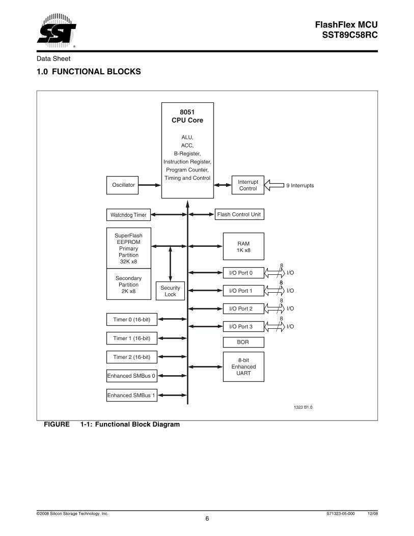
1.0 FUNCTIONAL BLOCKS
FIGURE 1-1: Functional Block Diagram
9 Interrupts
SuperFlashEEPROMPrimaryPartition32K x8
SecondaryPartition2K x8
I/O
I/O
I/O
I/O
Watchdog Timer
InterruptControl
8051CPU Core
RAM1K x8
SecurityLock
I/O Port 0
I/O Port 1
I/O Port 2
I/O Port 3
8-bitEnhanced
UART
BOR
Timer 0 (16-bit)
Timer 1 (16-bit)
Timer 2 (16-bit)
88
8
8
1323 B1.0
Enhanced SMBus 0
Flash Control Unit
8
Oscillator
Enhanced SMBus 1
ALU,
ACC,
B-Register,
Instruction Register,
Program Counter,
Timing and Control
6©2008 Silicon Storage Technology, Inc. S71323-05-000 12/08
Data Sheet
FlashFlex MCUSST89C58RC
2.0 PIN ASSIGNMENTS
FIGURE 2-1: Pin Assignments for 44-Lead TQFP
FIGURE 2-2: Pin Assignments for 44-Lead PLCC
(SDA1) P1.5
(SDA0) P1.6
(SCL0) P1.7
RST
(RXD) P3.0
NC
(TXD) P3.1
(INT0#) P3.2
(INT1#) P3.3
(T0) P3.4
( T1) P3.5
P0.4 (AD4)
P0.5 (AD5)
P0.6 (AD6)
P0.7 (AD7)
EA#
NC
ALE/PROG#
PSEN#
P2.7 (A15)
P2.6 (A14)
P2.5 (A13)
P1.
4 (S
CL1
)
P1.
3
P1.
2
P1.
1 (T
2 E
X)
P1.
0 (T
2)
NC
VD
D
P0.
0 (A
D0)
P0.
1 (A
D1)
P0.
2 (A
D2)
P0.
3 (A
D3)
(WR
#) P
3.6
(RD
#) P
3.7
XTA
L2
XTA
L1
VS
S
NC
(A8)
P2.
0
(A9)
P2.
1
(A10
) P2.
2
(A11
) P2.
3
(A12
) P2.
4
1323 44-tqfp TQJ P1.0
1
2
3
4
5
6
7
8
9
10
11
33
32
31
30
29
28
27
26
25
24
23
44 43 42 41 40 39 38 37 36 35 34
12 13 14 15 16 17 18 19 20 21 22
44-lead TQFPTop View
39
38
37
36
35
34
33
32
31
30
29
7
8
9
10
11
12
13
14
15
16
17
(SDA1) P1.5
(SDA0) P1.6
(SCL0) P1.7
RST
(RXD) P3.0
NC
(TXD) P3.1
(INT0#) P3.2
(INT1#) P3.3
(T0) P3.4
(T1) P3.5
P0.4 (AD4)
P0.5 (AD5)
P0.6 (AD6)
P0.7 (AD7)
EA#
NC
ALE/PROG#
PSEN#
P2.7 (A15)
P2.6 (A14)
P2.5 (A13)
6 5 4 3 2 1 44 43 42 41 40
18 19 20 21 22 23 24 25 26 27 28
P1.
4 (S
CL1
)
P1.
3
P1.
2
P1.
1 (T
2 E
X)
P1.
0 (T
2)
NC
VD
D
P0.
0 (A
D0)
P0.
1 (A
D1)
P0.
2 (A
D2)
P0.
3 (A
D3)
(WR
#) P
3.6
(RD
#) P
3.7
XTA
L2
XTA
L1
VS
S
NC
(A8)
P2.
0
(A9)
P2.
1
(A10
) P2.
2
(A11
) P2.
3
(A12
) P2.
4
44-lead PLCCTop View
1323 44-plcc NJ P2.0
7©2008 Silicon Storage Technology, Inc. S71323-05-000 12/08
Data Sheet
FlashFlex MCUSST89C58RC
FIGURE 2-3: Pin Assignments for 40-Contact WQFN
1323 40-wqfn QI P3.0
(SDA1) P1.5
(SDA0) P1.6
(SCL0) P1.7
RST
(RXD) P3.0
(TXD) P3.1
(INT0#) P3.2
(INT1#) P3.3
(T0) P3.4
(T1) P3.5
(WR
#) P
3.6
(RD
#) P
3.7
XTA
L2
XTA
L1
VS
S
(A8)
P2.
0
(A9)
P2.
1
(A10
) P
2.2
(A11
) P
2.3
(A12
) P
2.4
140
P0.4 (AD4)
P0.5 (AD5)
P0.6 (AD6)
P0.7 (AD7)
EA#
ALE/PROG#
PSEN#
P2.7 (A15)
P2.6 (A14)
P2.5 (A13)
P1.
4 (S
CL1
)
P1.
3
P1.
2
P1.
1 (T
2 E
X)
P1.
0 (T
2)
VD
D
P0.
0 (A
D0)
P0.
1 (A
D1)
P0.
2 (A
D2)
P0.
3 (A
D3)
Top View(contacts facing down)
8©2008 Silicon Storage Technology, Inc. S71323-05-000 12/08
Data Sheet
FlashFlex MCUSST89C58RC
2.1 Pin Descriptions
TABLE 2-1: Pin Descriptions (1 of 2)
Symbol Type1 Name and Functions
P0[7:0] I/O Port 0: Port 0 is an 8-bit open drain bi-directional I/O port. As an output port each pin can sink several LS TTL inputs. Port 0 pins that have ‘1’s written to them float, and in this state can be used as high-impedance inputs. Port 0 is also the multiplexed low-order address and data bus during accesses to external code and data memory. In this application, it uses strong internal pull-ups when transitioning to ‘1’s. External pull-ups are required as a general purpose I/O port.
P1[7:0] I/Owith internal
pull-up
Port 1: Port 1 is an 8-bit bi-directional I/O port with internal pull-ups. The Port 1 output buffers can drive LS TTL inputs. Port 1 pins are pulled high by the internal pull-ups when ‘1’s are written to them and can be used as inputs in this state. As inputs, Port 1 pins that are externally pulled low will source current because of the internal pull-ups.
P1[0] I/O T2: External count input to Timer/Counter 2 or Clock-out from Timer/Counter 2
P1[1] I T2EX: Timer/Counter 2 capture/reload trigger and direction control
P1[2] I/O GPIO
P1[3] I/O GPIO
P1[4] I/O SCL1: SMBus1 serial clock input / output
P1[5] I/O SDA1: SMBus1 serial data input / output
P1[6] I/O SDA0: SMBus0 serial data input / output
P1[7] I/O SCL0: SMBus1 serial clock input / output
P2[7:0] I/Owith internal
pull-up
Port 2: Port 2 is an 8-bit bi-directional I/O port with internal pull-ups. Port 2 pins are pulled high by the internal pull-ups when ‘1’s are written to them and can be used as inputs in this state. As inputs, Port 2 pins that are externally pulled low will source current because of the internal pull-ups. Port 2 sends the high-order address byte during accesses to external Data Memory that use 16-bit address (MOVX@DPTR). In this application, it uses strong internal pull-ups when transi-tioning to VOH.
P3[7:0] I/Owith internal
pull-up
Port 3: Port 3 is an 8-bit bi-directional I/O port with internal pull-ups. The Port 3 output buffers can drive LS TTL inputs. Port 3 pins are pulled high by the internal pull-ups when ‘1’s are written to them and can be used as inputs in this state. As inputs, Port 3 pins that are externally pulled low will source current because of the internal pull-ups.
P3[0] I RXD: Universal Asynchronous Receiver/Transmitter (UART) - Receive input
P3[1] O TXD: UART - Transmit output
P3[2] I INT0#: External Interrupt 0 Input
P3[3] I INT1#: External Interrupt 1 Input
P3[4] I T0: External count input to Timer/Counter 0
P3[5] I T1: External count input to Timer/Counter 1
P3[6] O WR#: External Data Memory Write strobe
P3[7] O RD#: External Data Memory Read strobe
PSEN# I/O Program Store Enable: PSEN# is the Read strobe to external program. When the device is exe-cuting from internal program memory, PSEN# is inactive (VOH).
RST I Reset: While the oscillator is running, a “high” logic state on this pin for two machine cycles will reset the device.
EA# I External Access Enable: EA# must be connected to VSS in order to enable the device to fetch code from the external program memory. EA# must be strapped to VDD for internal program exe-cution. However, Disable-Extern-Boot (See Section 8.0, “Security Lock”) will disable EA#, and program execution is only possible from internal program memory.
9©2008 Silicon Storage Technology, Inc. S71323-05-000 12/08

Data Sheet
FlashFlex MCUSST89C58RC
2.2 I/O DescriptionsThe device supports 2.7~5.5V supply, and the I/O pins cantolerate VDD +0.5V. However, applying any voltage beyondpower supply in quai-bidirectional mode is not recom-mended because doing so causes current to flow from thepin to VDD which consumes extra power.
ALE/PROG# I/O Address Latch Enable: ALE is the output signal for latching the low byte of the address during an access to external memory. This pin is also the programming pulse input (PROG#) for flash programming. Normally the ALE2 is emitted at a constant rate of 1/6 the crystal frequency3. One ALE pulse is skipped during each access to external data memory. However, if AO is set to ‘1’, ALE is disabled.
NC I/O No Connect
XTAL1 I Crystal 1: Input to the inverting oscillator amplifier and input to the internal clock generator cir-cuits.
XTAL2 O Crystal 2: Output from the inverting oscillator amplifier.
VDD I Power Supply
VSS I GroundT2-1.0 1323
1. I = Input; O = Output2.ALE loading issue: When ALE pin experiences higher loading (>30pf) during the reset, the MCU may accidentally enter into modes
other than normal working mode. The solution is to add a pull-up resistor of 3-50 KΩ to VDD, e.g. for ALE pin.3. For 6 clock mode, ALE is emitted at 1/3 of crystal frequency.
TABLE 2-1: Pin Descriptions (Continued) (2 of 2)
Symbol Type1 Name and Functions
10©2008 Silicon Storage Technology, Inc. S71323-05-000 12/08
Data Sheet
FlashFlex MCUSST89C58RC
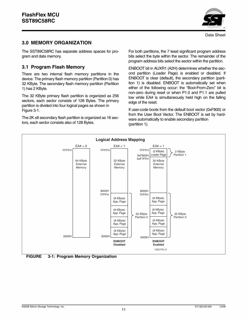
3.0 MEMORY ORGANIZATION
The SST89C58RC has separate address spaces for pro-gram and data memory.
3.1 Program Flash Memory There are two internal flash memory partitions in thedevice. The primary flash memory partition (Partition 0) has32 KByte. The secondary flash memory partition (Partition1) has 2 KByte.
The 32 KByte primary flash partition is organized as 256sectors, each sector consists of 128 Bytes. The primarypartition is divided into four logical pages as shown inFigure 3-1.
The 2K x8 secondary flash partition is organized as 16 sec-tors, each sector consists also of 128 Bytes.
For both partitions, the 7 least significant program addressbits select the byte within the sector. The remainder of theprogram address bits select the sector within the partition.
ENBOOT bit in AUXR1 (A2H) determines whether the sec-ond partition (Loader Page) is enabled or disabled. IfENBOOT is clear (default), the secondary partition (parti-tion 1) is disabled. ENBOOT is automatically set wheneither of the following occur: the “Boot-From-Zero” bit isnon-zero during reset or when P1.0 and P1.1 are pulledlow while EA# is simultaneously held high on the fallingedge of the reset.
If user-code boots from the default boot vector (0xF800) orfrom the User Boot Vector. The ENBOOT is set by hard-ware automatically to enable secondary partition (partition 1).
FIGURE 3-1: Program Memory Organization
1323 F01.0
(8 KByte)App. Page
30 KByteExternalMemory
Logical Address Mapping
64 KByteExternalMemory
EA# = 0FFFFH
0000H
EA# = 1 EA# = 1FFFFH
0000H
8000H7FFFH
32 KByteExternalMemory
FFFFH
0000H
(2 KByte)Loader Page
ENBOOTDisabled
ENBOOTEnabled
0xF800H0xF7FFH
(8 KByte)App. Page
(8 KByte)App. Page
(8 KByte)App. Page
(8 KByte)App. Page
(8 KByte)App. Page
(8 KByte)App. Page
(8 KByte)App. Page
8000H7FFFH
32 KBytePartition 0
32 KBytePartition 0
2 KBytePartition 1
11©2008 Silicon Storage Technology, Inc. S71323-05-000 12/08
Data Sheet
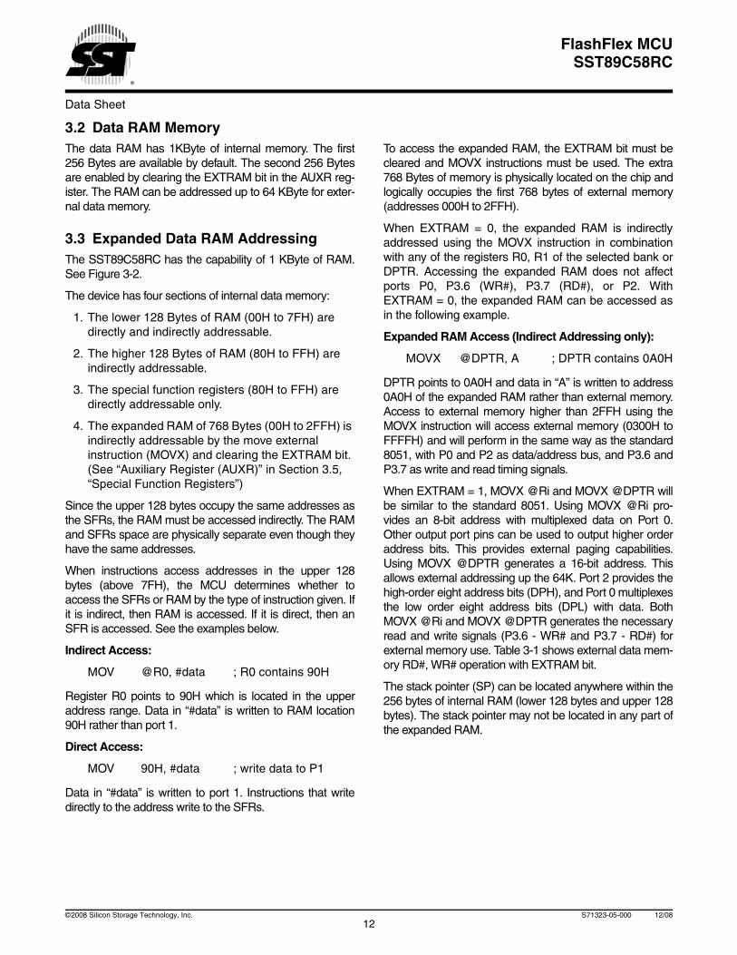
FlashFlex MCUSST89C58RC
3.2 Data RAM MemoryThe data RAM has 1KByte of internal memory. The first256 Bytes are available by default. The second 256 Bytesare enabled by clearing the EXTRAM bit in the AUXR reg-ister. The RAM can be addressed up to 64 KByte for exter-nal data memory.
3.3 Expanded Data RAM AddressingThe SST89C58RC has the capability of 1 KByte of RAM.See Figure 3-2.
The device has four sections of internal data memory:
1. The lower 128 Bytes of RAM (00H to 7FH) are directly and indirectly addressable.
2. The higher 128 Bytes of RAM (80H to FFH) are indirectly addressable.
3. The special function registers (80H to FFH) are directly addressable only.
4. The expanded RAM of 768 Bytes (00H to 2FFH) is indirectly addressable by the move external instruction (MOVX) and clearing the EXTRAM bit. (See “Auxiliary Register (AUXR)” in Section 3.5, “Special Function Registers”)
Since the upper 128 bytes occupy the same addresses asthe SFRs, the RAM must be accessed indirectly. The RAMand SFRs space are physically separate even though theyhave the same addresses.
When instructions access addresses in the upper 128bytes (above 7FH), the MCU determines whether toaccess the SFRs or RAM by the type of instruction given. Ifit is indirect, then RAM is accessed. If it is direct, then anSFR is accessed. See the examples below.
Indirect Access:
MOV @R0, #data ; R0 contains 90H
Register R0 points to 90H which is located in the upperaddress range. Data in “#data” is written to RAM location90H rather than port 1.
Direct Access:
MOV 90H, #data ; write data to P1
Data in “#data” is written to port 1. Instructions that writedirectly to the address write to the SFRs.
To access the expanded RAM, the EXTRAM bit must becleared and MOVX instructions must be used. The extra768 Bytes of memory is physically located on the chip andlogically occupies the first 768 bytes of external memory(addresses 000H to 2FFH).
When EXTRAM = 0, the expanded RAM is indirectlyaddressed using the MOVX instruction in combinationwith any of the registers R0, R1 of the selected bank orDPTR. Accessing the expanded RAM does not affectports P0, P3.6 (WR#), P3.7 (RD#), or P2. WithEXTRAM = 0, the expanded RAM can be accessed asin the following example.
Expanded RAM Access (Indirect Addressing only):
MOVX @DPTR, A ; DPTR contains 0A0H
DPTR points to 0A0H and data in “A” is written to address0A0H of the expanded RAM rather than external memory.Access to external memory higher than 2FFH using theMOVX instruction will access external memory (0300H toFFFFH) and will perform in the same way as the standard8051, with P0 and P2 as data/address bus, and P3.6 andP3.7 as write and read timing signals.
When EXTRAM = 1, MOVX @Ri and MOVX @DPTR willbe similar to the standard 8051. Using MOVX @Ri pro-vides an 8-bit address with multiplexed data on Port 0.Other output port pins can be used to output higher orderaddress bits. This provides external paging capabilities.Using MOVX @DPTR generates a 16-bit address. Thisallows external addressing up the 64K. Port 2 provides thehigh-order eight address bits (DPH), and Port 0 multiplexesthe low order eight address bits (DPL) with data. BothMOVX @Ri and MOVX @DPTR generates the necessaryread and write signals (P3.6 - WR# and P3.7 - RD#) forexternal memory use. Table 3-1 shows external data mem-ory RD#, WR# operation with EXTRAM bit.
The stack pointer (SP) can be located anywhere within the256 bytes of internal RAM (lower 128 bytes and upper 128bytes). The stack pointer may not be located in any part ofthe expanded RAM.
12©2008 Silicon Storage Technology, Inc. S71323-05-000 12/08

Data Sheet
FlashFlex MCUSST89C58RC
FIGURE 3-2: Internal and External Data Memory Structure
TABLE 3-1: External Data Memory RD#, WR# with EXTRAM bit
MOVX @DPTR, A or MOVX A, @DPTR MOVX @Ri, A or MOVX A, @Ri
AUXR ADDR < 0300H ADDR >= 0300H ADDR = Any
EXTRAM = 0 RD# / WR# not asserted RD# / WR# asserted RD# / WR# not asserted1
EXTRAM = 1 RD# / WR# asserted RD# / WR# asserted RD# / WR# assertedT3-1.0 1323
1. Access limited to ERAM address within 0 to 0FFH. 100H to 02FFH is not accessible.
000H
2FFH
00H
FFH
Upper 128 BytesInternal RAM
Lower 128 BytesInternal RAM
(Indirect & DirectAddressing)
(Indirect Addressing) (Direct Addressing)
SpecialFunctionRegisters(SFRs)
80H
FFH
FFFFH
000H
ExternalData
Memory
2FFH
0000H
ExternalData
Memory
EXTRAM = 0 EXTRAM = 1
Expanded RAM
0300H
(Indirect Addressing)
FFFFH(Indirect Addressing) (Indirect Addressing)
80H7FH
1294 F02.0
ExpandedRAM
768 Bytes
13©2008 Silicon Storage Technology, Inc. S71323-05-000 12/08
Data Sheet
FlashFlex MCUSST89C58RC
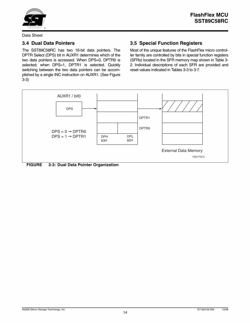
3.4 Dual Data PointersThe SST89C58RC has two 16-bit data pointers. TheDPTR Select (DPS) bit in AUXR1 determines which of thetwo data pointers is accessed. When DPS=0, DPTR0 isselected; when DPS=1, DPTR1 is selected. Quicklyswitching between the two data pointers can be accom-plished by a single INC instruction on AUXR1. (See Figure3-3)
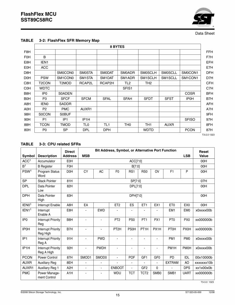
3.5 Special Function RegistersMost of the unique features of the FlashFlex micro control-ler family are controlled by bits in special function registers(SFRs) located in the SFR memory map shown in Table 3-2. Individual descriptions of each SFR are provided andreset values indicated in Tables 3-3 to 3-7.
FIGURE 3-3: Dual Data Pointer Organization
DPL82H
External Data Memory
DPS
1323 F03.0
DPH83H
DPTR0
DPTR1
AUXR1 / bit0
DPS = 0 DPTR0DPS = 1 DPTR1
14©2008 Silicon Storage Technology, Inc. S71323-05-000 12/08
Data Sheet
FlashFlex MCUSST89C58RC
TABLE 3-2: FlashFlex SFR Memory Map
8 BYTES
F8H FFH
F0H B F7H
E8H IEN1 EFH
E0H ACC E7H
D8H SM0CON0 SM0STA SM0DAT SM0ADR SM0SCLH SM0SCLL SM0CON1 DFH
D0H PSW SM1CON0 SM1STA SM1DAT SM1ADR SM1SCLH SM1SCLL SM1CON1 D7H
C8H T2CON T2MOD RCAP2L RCAP2H TL2 TH2 CFH
C0H WDTC SFIS1 C7H
B8H IP0 S0ADEN COSR BFH
B0H P3 SFCF SFCM SFAL SFAH SFDT SFST IP0H B7H
A8H IEN0 SADDR AFH
A0H P2 PMC AUXR1 A7H
98H S0CON S0BUF 9FH
90H P1 IP1 IP1H SFISO 97H
88H TCON TMOD TL0 TL1 TH0 TH1 AUXR 8FH
80H P0 SP DPL DPH WDTD PCON 87HT3-2.0 1323
TABLE 3-3: CPU related SFRs
Symbol DescriptionDirect
Address
Bit Address, Symbol, or Alternative Port Function ResetValueMSB LSB
ACC1 Accumulator E0H ACC[7:0] 00H
B1 B Register F0H B[7:0] 00H
PSW1 Program StatusWord
D0H CY AC F0 RS1 RS0 OV F1 P 00H
SP Stack Pointer 81H SP[7:0] 07H
DPL Data PointerLow
82H DPL[7:0] 00H
DPH Data PointerHigh
83H DPH[7:0] 00H
IEN01 Interrupt Enable A8H EA ET2 ES ET1 EX1 ET0 EX0 00H
IEN11 InterruptEnable A
E8H - EWD - - - - EM1 EM0 x0xxxx00b
IP0 Interrupt PriorityReg
B8H - - PT2 PS0 PT1 PX1 PT0 PX0 xx000000b
IP0H Interrupt PriorityReg High
B7H - - PT2H PS0H PT1H PX1H PT0H PX0H xx000000b
IP1 Interrupt PriorityReg A
91H - PWD - - - - PM1 PM0 x0xxxx00b
IP1H Interrupt PriorityReg A High
92H - PWDH - - - - PM1H PM0H x0xxxx00b
PCON Power Control 87H SMOD1 SMOD0 - POF GF1 GF0 PD IDL 00x10000b
AUXR Auxiliary Reg 8EH - - - - - - EXTRAM AO xxxxxxx10b
AUXR1 Auxiliary Reg 1 A2H - - ENBOOT - GF2 0 - DPS xx1x00x0b
PMC Power Manage-ment Control
A1H - - WDU TCT TCT2 SMB0 SMB1 UART xx000000b
T3-3.0 1323
15©2008 Silicon Storage Technology, Inc. S71323-05-000 12/08
Data Sheet
FlashFlex MCUSST89C58RC
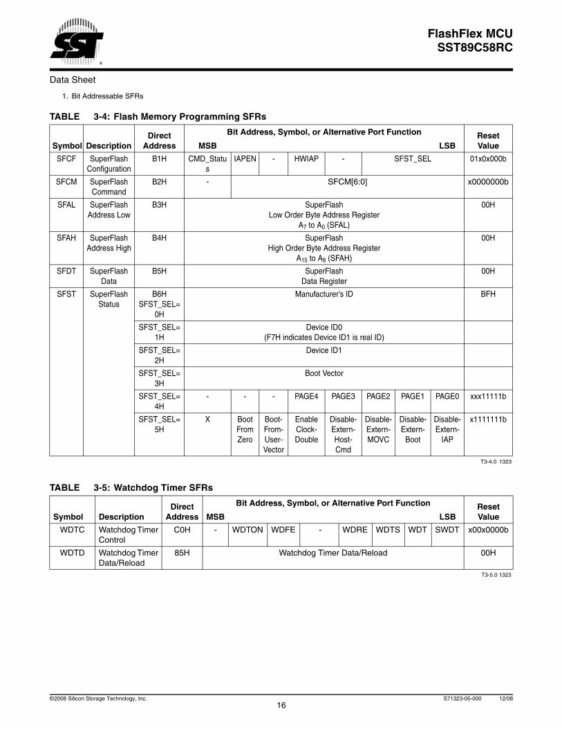
1. Bit Addressable SFRs
TABLE 3-4: Flash Memory Programming SFRs
Symbol DescriptionDirect
Address
Bit Address, Symbol, or Alternative Port Function ResetValueMSB LSB
SFCF SuperFlashConfiguration
B1H CMD_Status
IAPEN - HWIAP - SFST_SEL 01x0x000b
SFCM SuperFlashCommand
B2H - SFCM[6:0] x0000000b
SFAL SuperFlashAddress Low
B3H SuperFlashLow Order Byte Address Register
A7 to A0 (SFAL)
00H
SFAH SuperFlashAddress High
B4H SuperFlashHigh Order Byte Address Register
A15 to A8 (SFAH)
00H
SFDT SuperFlashData
B5H SuperFlashData Register
00H
SFST SuperFlashStatus
B6HSFST_SEL=
0H
Manufacturer’s ID BFH
SFST_SEL=1H
Device ID0(F7H indicates Device ID1 is real ID)
SFST_SEL=2H
Device ID1
SFST_SEL=3H
Boot Vector
SFST_SEL=4H
- - - PAGE4 PAGE3 PAGE2 PAGE1 PAGE0 xxx11111b
SFST_SEL=5H
X BootFromZero
Boot-From-User-Vector
EnableClock-Double
Disable-Extern-Host-Cmd
Disable-Extern-MOVC
Disable-Extern-
Boot
Disable-Extern-
IAP
x1111111b
T3-4.0 1323
TABLE 3-5: Watchdog Timer SFRs
Symbol DescriptionDirect
Address
Bit Address, Symbol, or Alternative Port Function ResetValueMSB LSB
WDTC Watchdog Timer Control
C0H - WDTON WDFE - WDRE WDTS WDT SWDT x00x0000b
WDTD Watchdog Timer Data/Reload
85H Watchdog Timer Data/Reload 00H
T3-5.0 1323
16©2008 Silicon Storage Technology, Inc. S71323-05-000 12/08
Data Sheet
FlashFlex MCUSST89C58RC
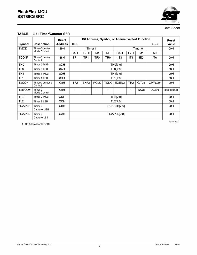
TABLE 3-6: Timer/Counter SFR
Symbol DescriptionDirect
Address
Bit Address, Symbol, or Alternative Port Function ResetValueMSB LSB
TMOD Timer/Counter Mode Control
89H Timer 1 Timer 0 00H
GATE C/T# M1 M0 GATE C/T# M1 M0
TCON1 Timer/Counter Control
88H TF1 TR1 TF0 TR0 IE1 IT1 IE0 IT0 00H
TH0 Timer 0 MSB 8CH TH0[7:0] 00H
TL0 Timer 0 LSB 8AH TL0[7:0] 00H
TH1 Timer 1 MSB 8DH TH1[7:0] 00H
TL1 Timer 1 LSB 8BH TL1[7:0] 00H
T2CON1 Timer/Counter 2Control
C8H TF2 EXF2 RCLK TCLK EXEN2 TR2 C/T2# CP/RL2# 00H
T2MOD# Timer 2Mode Control
C9H - - - - - - T2OE DCEN xxxxxx00b
TH2 Timer 2 MSB CDH TH2[7:0] 00H
TL2 Timer 2 LSB CCH TL2[7:0] 00H
RCAP2H Timer 2 Capture MSB
CBH RCAP2H[7:0] 00H
RCAP2L Timer 2 Capture LSB
CAH RCAP2L[7:0] 00H
T3-6.0 13231. Bit Addressable SFRs
17©2008 Silicon Storage Technology, Inc. S71323-05-000 12/08
Data Sheet
FlashFlex MCUSST89C58RC
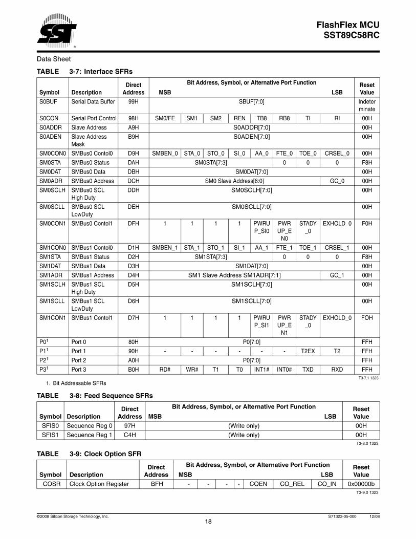
TABLE 3-7: Interface SFRs
Symbol DescriptionDirect
Address
Bit Address, Symbol, or Alternative Port Function ResetValueMSB LSB
S0BUF Serial Data Buffer 99H SBUF[7:0] Indeterminate
S0CON Serial Port Control 98H SM0/FE SM1 SM2 REN TB8 RB8 TI RI 00H
S0ADDR Slave Address A9H S0ADDR[7:0] 00H
S0ADEN Slave AddressMask
B9H S0ADEN[7:0] 00H
SM0CON0 SMBus0 Contol0 D9H SMBEN_0 STA_0 STO_0 SI_0 AA_0 FTE_0 TOE_0 CRSEL_0 00H
SM0STA SMBus0 Status DAH SM0STA[7:3] 0 0 0 F8H
SM0DAT SMBus0 Data DBH SM0DAT[7:0] 00H
SM0ADR SMBus0 Address DCH SM0 Slave Address[6:0] GC_0 00H
SM0SCLH SMBus0 SCL High Duty
DDH SM0SCLH[7:0] 00H
SM0SCLL SMBus0 SCL LowDuty
DEH SM0SCLL[7:0] 00H
SM0CON1 SMBus0 Contol1 DFH 1 1 1 1 PWRUP_SI0
PWR UP_E
N0
STADY_0
EXHOLD_0 F0H
SM1CON0 SMBus1 Contol0 D1H SMBEN_1 STA_1 STO_1 SI_1 AA_1 FTE_1 TOE_1 CRSEL_1 00H
SM1STA SMBus1 Status D2H SM1STA[7:3] 0 0 0 F8H
SM1DAT SMBus1 Data D3H SM1DAT[7:0] 00H
SM1ADR SMBus1 Address D4H SM1 Slave Address SM1ADR[7:1] GC_1 00H
SM1SCLH SMBus1 SCL High Duty
D5H SM1SCLH[7:0] 00H
SM1SCLL SMBus1 SCL LowDuty
D6H SM1SCLL[7:0] 00H
SM1CON1 SMBus1 Contol1 D7H 1 1 1 1 PWRUP_SI1
PWR UP_E
N1
STADY_0
EXHOLD_0 FOH
P01 Port 0 80H P0[7:0] FFH
P11 Port 1 90H - - - - - - T2EX T2 FFH
P21 Port 2 A0H P0[7:0] FFH
P31 Port 3 B0H RD# WR# T1 T0 INT1# INT0# TXD RXD FFHT3-7.1 1323
1. Bit Addressable SFRs
TABLE 3-8: Feed Sequence SFRs
Symbol DescriptionDirect
Address
Bit Address, Symbol, or Alternative Port Function ResetValueMSB LSB
SFIS0 Sequence Reg 0 97H (Write only) 00H
SFIS1 Sequence Reg 1 C4H (Write only) 00HT3-8.0 1323
TABLE 3-9: Clock Option SFR
Symbol DescriptionDirect
Address
Bit Address, Symbol, or Alternative Port Function ResetValueMSB LSB
COSR Clock Option Register BFH - - - - COEN CO_REL CO_IN 0x00000bT3-9.0 1323
18©2008 Silicon Storage Technology, Inc. S71323-05-000 12/08
Data Sheet
FlashFlex MCUSST89C58RC
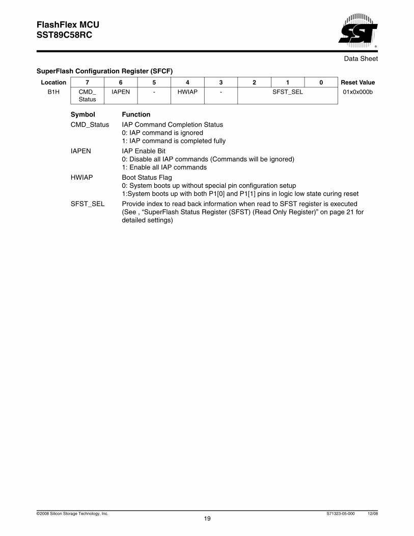
Symbol Function
CMD_Status IAP Command Completion Status0: IAP command is ignored1: IAP command is completed fully
IAPEN IAP Enable Bit0: Disable all IAP commands (Commands will be ignored)1: Enable all IAP commands
HWIAP Boot Status Flag0: System boots up without special pin configuration setup1:System boots up with both P1[0] and P1[1] pins in logic low state curing reset
SFST_SEL Provide index to read back information when read to SFST register is executed(See , “SuperFlash Status Register (SFST) (Read Only Register)” on page 21 for detailed settings)
SuperFlash Configuration Register (SFCF)
Location 7 6 5 4 3 2 1 0 Reset Value
B1H CMD_Status
IAPEN - HWIAP - SFST_SEL 01x0x000b
19©2008 Silicon Storage Technology, Inc. S71323-05-000 12/08
Data Sheet
FlashFlex MCUSST89C58RC
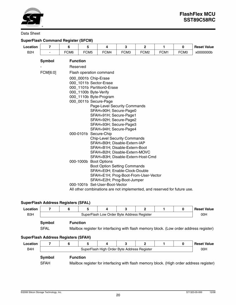
Symbol Function
- Reserved
FCM[6:0] Flash operation command
000_0001b Chip-Erase000_1011b Sector-Erase000_1101b Partition0-Erase000_1100b Byte-Verify000_1110b Byte-Program000_0011b Secure-Page
Page-Level Security CommandsSFAH=90H; Secure-Page0SFAH=91H; Secure-Page1SFAH=92H; Secure-Page2SFAH=93H; Secure-Page3SFAH=94H; Secure-Page4
000-0101b Secure-ChipChip-Level Security CommandsSFAH=B0H; Disable-Extern-IAPSFAH=B1H; Disable-Extern-BootSFAH=B2H; Disable-Extern-MOVCSFAH=B3H; Disable-Extern-Host-Cmd
000-1000b Boot OptionsBoot Option Setting CommandsSFAH=E0H; Enable-Clock-DoubleSFAH=E1H; Prog-Boot-From-User-VectorSFAH=E2H; Prog-Boot-Jumper
000-1001b Set-User-Boot-VectorAll other combinations are not implemented, and reserved for future use.
Symbol Function
SFAL Mailbox register for interfacing with flash memory block. (Low order address register)
Symbol Function
SFAH Mailbox register for interfacing with flash memory block. (High order address register)
SuperFlash Command Register (SFCM)
Location 7 6 5 4 3 2 1 0 Reset Value
B2H - FCM6 FCM5 FCM4 FCM3 FCM2 FCM1 FCM0 x0000000b
SuperFlash Address Registers (SFAL)
Location 7 6 5 4 3 2 1 0 Reset Value
B3H SuperFlash Low Order Byte Address Register 00H
SuperFlash Address Registers (SFAH)
Location 7 6 5 4 3 2 1 0 Reset Value
B4H SuperFlash High Order Byte Address Register 00H
20©2008 Silicon Storage Technology, Inc. S71323-05-000 12/08
Data Sheet
FlashFlex MCUSST89C58RC
Symbol Function
SFDT Mailbox register for interfacing with flash memory block. (Data register)
Symbol Function
SFST This is a read-only register. The read-back value is indexed by SFST_SEL in the SuperFlash Configuration Register (SFCF)
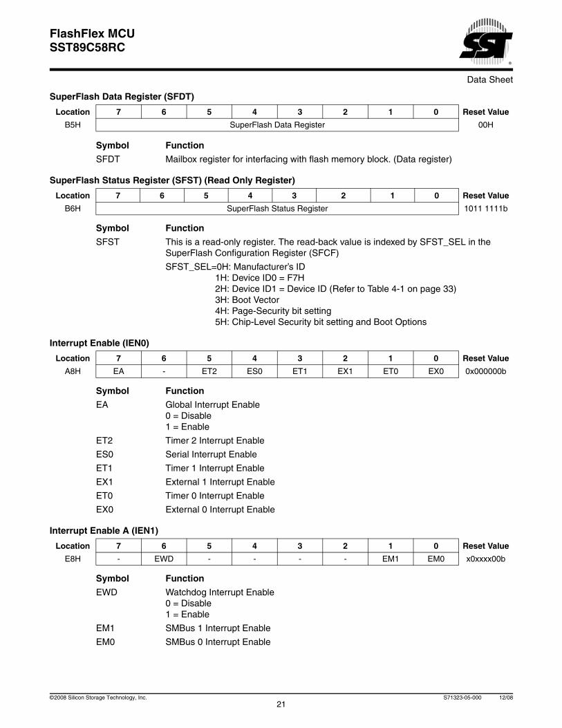
SFST_SEL=0H: Manufacturer’s ID1H: Device ID0 = F7H2H: Device ID1 = Device ID (Refer to Table 4-1 on page 33)3H: Boot Vector4H: Page-Security bit setting5H: Chip-Level Security bit setting and Boot Options
Symbol Function
EA Global Interrupt Enable0 = Disable1 = Enable
ET2 Timer 2 Interrupt Enable
ES0 Serial Interrupt Enable
ET1 Timer 1 Interrupt Enable
EX1 External 1 Interrupt Enable
ET0 Timer 0 Interrupt Enable
EX0 External 0 Interrupt Enable
Symbol Function
EWD Watchdog Interrupt Enable0 = Disable1 = Enable
EM1 SMBus 1 Interrupt Enable
EM0 SMBus 0 Interrupt Enable
SuperFlash Data Register (SFDT)
Location 7 6 5 4 3 2 1 0 Reset Value
B5H SuperFlash Data Register 00H
SuperFlash Status Register (SFST) (Read Only Register)
Location 7 6 5 4 3 2 1 0 Reset Value
B6H SuperFlash Status Register 1011 1111b
Interrupt Enable (IEN0)
Location 7 6 5 4 3 2 1 0 Reset Value
A8H EA - ET2 ES0 ET1 EX1 ET0 EX0 0x000000b
Interrupt Enable A (IEN1)
Location 7 6 5 4 3 2 1 0 Reset Value
E8H - EWD - - - - EM1 EM0 x0xxxx00b
21©2008 Silicon Storage Technology, Inc. S71323-05-000 12/08
Data Sheet
FlashFlex MCUSST89C58RC
Symbol Function
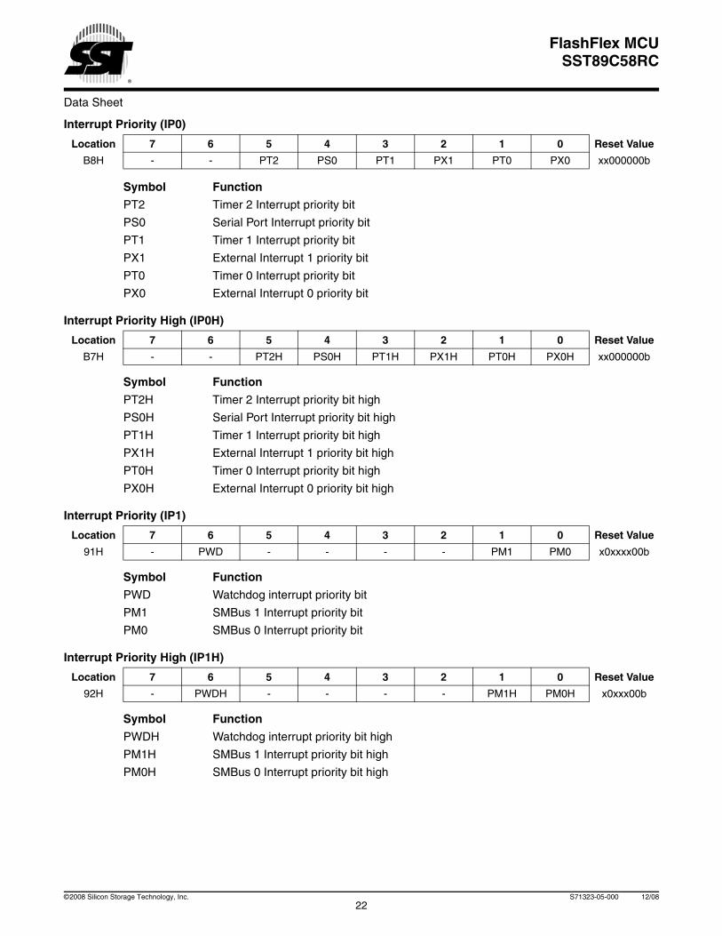
PT2 Timer 2 Interrupt priority bit
PS0 Serial Port Interrupt priority bit
PT1 Timer 1 Interrupt priority bit
PX1 External Interrupt 1 priority bit
PT0 Timer 0 Interrupt priority bit
PX0 External Interrupt 0 priority bit
Symbol Function
PT2H Timer 2 Interrupt priority bit high
PS0H Serial Port Interrupt priority bit high
PT1H Timer 1 Interrupt priority bit high
PX1H External Interrupt 1 priority bit high
PT0H Timer 0 Interrupt priority bit high
PX0H External Interrupt 0 priority bit high
Symbol Function
PWD Watchdog interrupt priority bit
PM1 SMBus 1 Interrupt priority bit
PM0 SMBus 0 Interrupt priority bit
Symbol Function
PWDH Watchdog interrupt priority bit high
PM1H SMBus 1 Interrupt priority bit high
PM0H SMBus 0 Interrupt priority bit high
Interrupt Priority (IP0)
Location 7 6 5 4 3 2 1 0 Reset Value
B8H - - PT2 PS0 PT1 PX1 PT0 PX0 xx000000b
Interrupt Priority High (IP0H)
Location 7 6 5 4 3 2 1 0 Reset Value
B7H - - PT2H PS0H PT1H PX1H PT0H PX0H xx000000b
Interrupt Priority (IP1)
Location 7 6 5 4 3 2 1 0 Reset Value
91H - PWD - - - - PM1 PM0 x0xxxx00b
Interrupt Priority High (IP1H)
Location 7 6 5 4 3 2 1 0 Reset Value
92H - PWDH - - - - PM1H PM0H x0xxx00b
22©2008 Silicon Storage Technology, Inc. S71323-05-000 12/08
Data Sheet
FlashFlex MCUSST89C58RC
Symbol Function
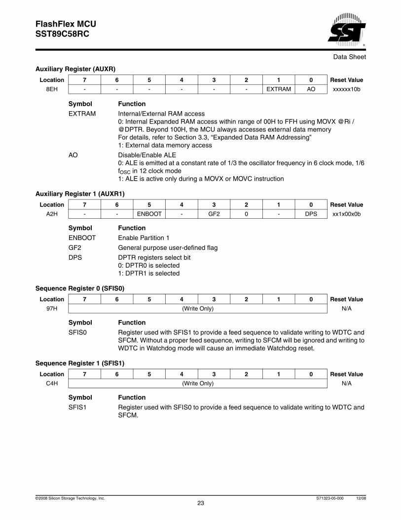
EXTRAM Internal/External RAM access0: Internal Expanded RAM access within range of 00H to FFH using MOVX @Ri / @DPTR. Beyond 100H, the MCU always accesses external data memory For details, refer to Section 3.3, “Expanded Data RAM Addressing” 1: External data memory access
AO Disable/Enable ALE0: ALE is emitted at a constant rate of 1/3 the oscillator frequency in 6 clock mode, 1/6 fOSC in 12 clock mode 1: ALE is active only during a MOVX or MOVC instruction
Symbol Function
ENBOOT Enable Partition 1
GF2 General purpose user-defined flag
DPS DPTR registers select bit0: DPTR0 is selected1: DPTR1 is selected
Symbol Function
SFIS0 Register used with SFIS1 to provide a feed sequence to validate writing to WDTC and SFCM. Without a proper feed sequence, writing to SFCM will be ignored and writing to WDTC in Watchdog mode will cause an immediate Watchdog reset.
Symbol Function
SFIS1 Register used with SFIS0 to provide a feed sequence to validate writing to WDTC and SFCM.
Auxiliary Register (AUXR)
Location 7 6 5 4 3 2 1 0 Reset Value
8EH - - - - - - EXTRAM AO xxxxxx10b
Auxiliary Register 1 (AUXR1)
Location 7 6 5 4 3 2 1 0 Reset Value
A2H - - ENBOOT - GF2 0 - DPS xx1x00x0b
Sequence Register 0 (SFIS0)
Location 7 6 5 4 3 2 1 0 Reset Value
97H (Write Only) N/A
Sequence Register 1 (SFIS1)
Location 7 6 5 4 3 2 1 0 Reset Value
C4H (Write Only) N/A
23©2008 Silicon Storage Technology, Inc. S71323-05-000 12/08
Data Sheet
FlashFlex MCUSST89C58RC
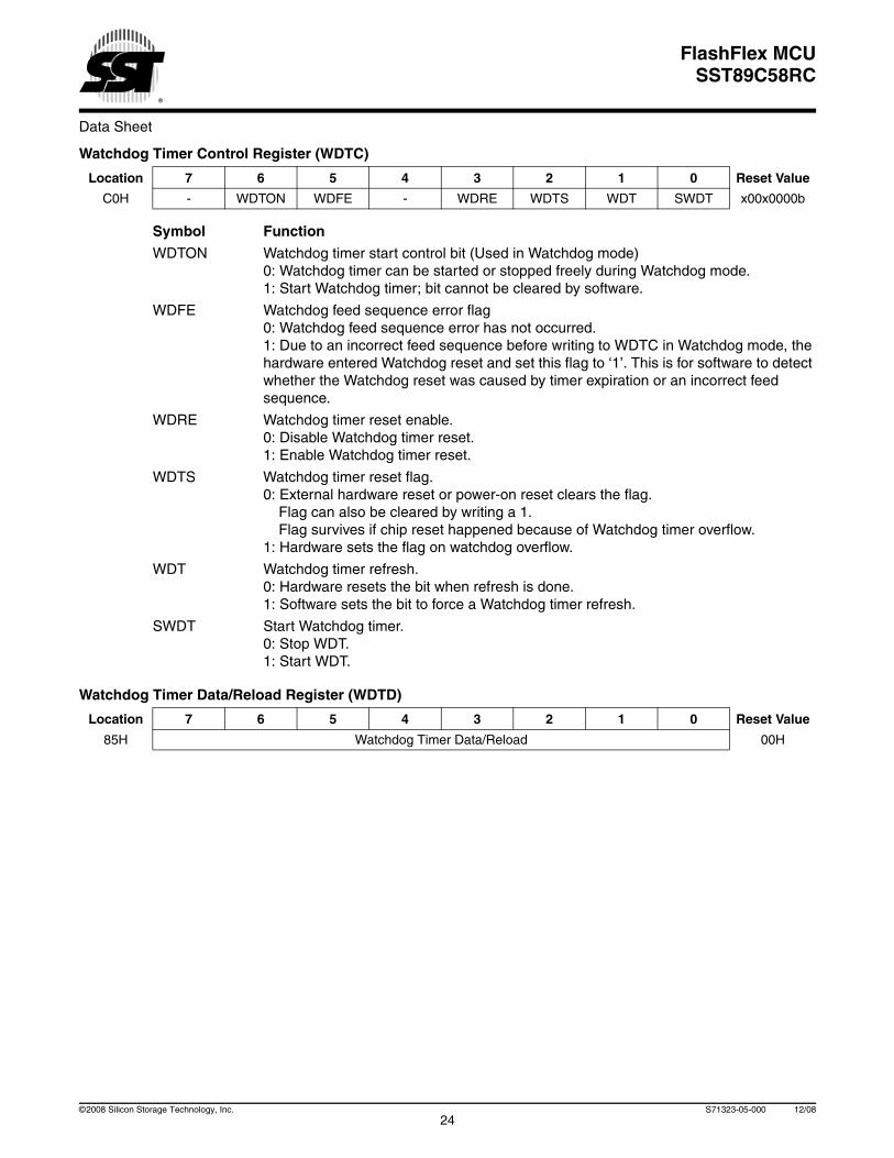
Symbol Function
WDTON Watchdog timer start control bit (Used in Watchdog mode)0: Watchdog timer can be started or stopped freely during Watchdog mode.1: Start Watchdog timer; bit cannot be cleared by software.
WDFE Watchdog feed sequence error flag0: Watchdog feed sequence error has not occurred.1: Due to an incorrect feed sequence before writing to WDTC in Watchdog mode, the hardware entered Watchdog reset and set this flag to ‘1’. This is for software to detect whether the Watchdog reset was caused by timer expiration or an incorrect feed sequence.
WDRE Watchdog timer reset enable.0: Disable Watchdog timer reset.1: Enable Watchdog timer reset.
WDTS Watchdog timer reset flag.0: External hardware reset or power-on reset clears the flag.
Flag can also be cleared by writing a 1.Flag survives if chip reset happened because of Watchdog timer overflow.
1: Hardware sets the flag on watchdog overflow.
WDT Watchdog timer refresh.0: Hardware resets the bit when refresh is done.1: Software sets the bit to force a Watchdog timer refresh.
SWDT Start Watchdog timer.0: Stop WDT.1: Start WDT.
Watchdog Timer Control Register (WDTC)
Location 7 6 5 4 3 2 1 0 Reset Value
C0H - WDTON WDFE - WDRE WDTS WDT SWDT x00x0000b
Watchdog Timer Data/Reload Register (WDTD)
Location 7 6 5 4 3 2 1 0 Reset Value
85H Watchdog Timer Data/Reload 00H
24©2008 Silicon Storage Technology, Inc. S71323-05-000 12/08
Data Sheet
FlashFlex MCUSST89C58RC
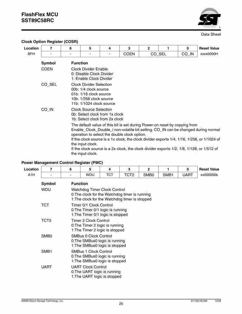
Symbol Function
COEN Clock Divider Enable0: Disable Clock Divider1: Enable Clock Divider
CO_SEL Clock Divider Selection00b: 1/4 clock source01b: 1/16 clock source10b: 1/256 clock source11b: 1/1024 clock source
CO_IN Clock Source Selection0b: Select clock from 1x clock1b: Select clock from 2x clock
The default value of this bit is set during Power-on reset by copying from Enable_Clock_Double_i non-volatile bit setting. CO_IN can be changed during normal operation to select the double clock option.If the clock source is a 1x clock, the clock divider exports 1/4, 1/16, 1/256, or 1/1024 of the input clock.If the clock source is a 2x clock, the clock divider exports 1/2, 1/8, 1/128, or 1/512 of the input clock.
Symbol Function
WDU Watchdog Timer Clock Control0:The clock for the Watchdog timer is running1:The clock for the Watchdog timer is stopped
TCT Timer 0/1 Clock Control0:The Timer 0/1 logic is running1:The Timer 0/1 logic is stopped
TCT2 Timer 2 Clock Control0:The Timer 2 logic is running1:The Timer 2 logic is stopped
SMB0 SMBus 0 Clock Control0:The SMBus0 logic is running1:The SMBus0 logic is stopped
SMB1 SMBus 1 Clock Control0:The SMBus0 logic is running1:The SMBus0 logic is stopped
UART UART Clock Control0:The UART logic is running1:The UART logic is stopped
Clock Option Register (COSR)
Location 7 6 5 4 3 2 1 0 Reset Value
BFH - - - - COEN CO_SEL CO_IN xxxx0000H
Power Management Control Register (PMC)
Location 7 6 5 4 3 2 1 0 Reset Value
A1H - - WDU TCT TCT2 SMB0 SMB1 UART xx000000b
25©2008 Silicon Storage Technology, Inc. S71323-05-000 12/08
Data Sheet
FlashFlex MCUSST89C58RC
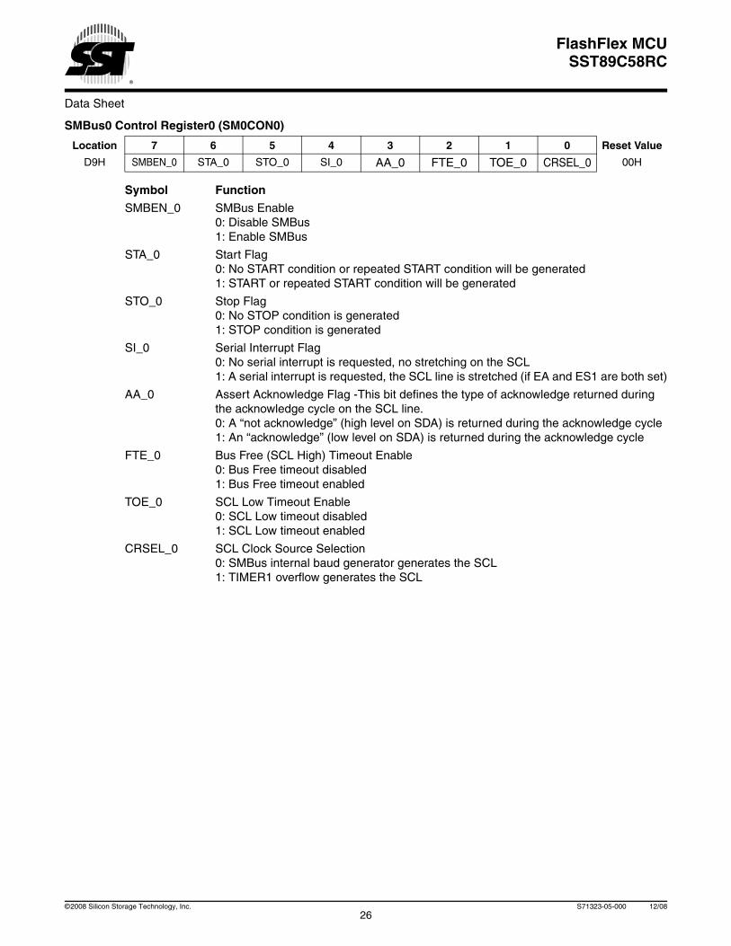
Symbol Function
SMBEN_0 SMBus Enable0: Disable SMBus1: Enable SMBus
STA_0 Start Flag0: No START condition or repeated START condition will be generated1: START or repeated START condition will be generated
STO_0 Stop Flag0: No STOP condition is generated1: STOP condition is generated
SI_0 Serial Interrupt Flag0: No serial interrupt is requested, no stretching on the SCL1: A serial interrupt is requested, the SCL line is stretched (if EA and ES1 are both set)
AA_0 Assert Acknowledge Flag -This bit defines the type of acknowledge returned during the acknowledge cycle on the SCL line.0: A “not acknowledge” (high level on SDA) is returned during the acknowledge cycle1: An “acknowledge” (low level on SDA) is returned during the acknowledge cycle
FTE_0 Bus Free (SCL High) Timeout Enable0: Bus Free timeout disabled1: Bus Free timeout enabled
TOE_0 SCL Low Timeout Enable0: SCL Low timeout disabled1: SCL Low timeout enabled
CRSEL_0 SCL Clock Source Selection0: SMBus internal baud generator generates the SCL1: TIMER1 overflow generates the SCL
SMBus0 Control Register0 (SM0CON0)
Location 7 6 5 4 3 2 1 0 Reset Value
D9H SMBEN_0 STA_0 STO_0 SI_0 AA_0 FTE_0 TOE_0 CRSEL_0 00H
26©2008 Silicon Storage Technology, Inc. S71323-05-000 12/08
Data Sheet
FlashFlex MCUSST89C58RC
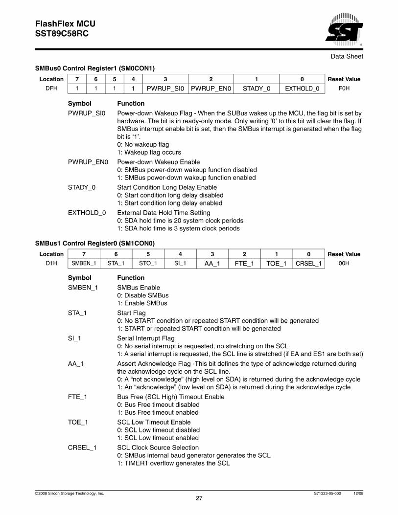
Symbol Function
PWRUP_SI0 Power-down Wakeup Flag - When the SUBus wakes up the MCU, the flag bit is set by hardware. The bit is in ready-only mode. Only writing ‘0’ to this bit will clear the flag. If SMBus interrupt enable bit is set, then the SMBus interrupt is generated when the flag bit is ‘1’.0: No wakeup flag1: Wakeup flag occurs
PWRUP_EN0 Power-down Wakeup Enable0: SMBus power-down wakeup function disabled1: SMBus power-down wakeup function enabled
STADY_0 Start Condition Long Delay Enable0: Start condition long delay disabled1: Start condition long delay enabled
EXTHOLD_0 External Data Hold Time Setting0: SDA hold time is 20 system clock periods1: SDA hold time is 3 system clock periods
Symbol Function
SMBEN_1 SMBus Enable0: Disable SMBus1: Enable SMBus
STA_1 Start Flag0: No START condition or repeated START condition will be generated1: START or repeated START condition will be generated
SI_1 Serial Interrupt Flag0: No serial interrupt is requested, no stretching on the SCL1: A serial interrupt is requested, the SCL line is stretched (if EA and ES1 are both set)
AA_1 Assert Acknowledge Flag -This bit defines the type of acknowledge returned during the acknowledge cycle on the SCL line.0: A “not acknowledge” (high level on SDA) is returned during the acknowledge cycle1: An “acknowledge” (low level on SDA) is returned during the acknowledge cycle
FTE_1 Bus Free (SCL High) Timeout Enable0: Bus Free timeout disabled1: Bus Free timeout enabled
TOE_1 SCL Low Timeout Enable0: SCL Low timeout disabled1: SCL Low timeout enabled
CRSEL_1 SCL Clock Source Selection0: SMBus internal baud generator generates the SCL1: TIMER1 overflow generates the SCL
SMBus0 Control Register1 (SM0CON1)
Location 7 6 5 4 3 2 1 0 Reset Value
DFH 1 1 1 1 PWRUP_SI0 PWRUP_EN0 STADY_0 EXTHOLD_0 F0H
SMBus1 Control Register0 (SM1CON0)
Location 7 6 5 4 3 2 1 0 Reset Value
D1H SMBEN_1 STA_1 STO_1 SI_1 AA_1 FTE_1 TOE_1 CRSEL_1 00H
27©2008 Silicon Storage Technology, Inc. S71323-05-000 12/08
Data Sheet
FlashFlex MCUSST89C58RC
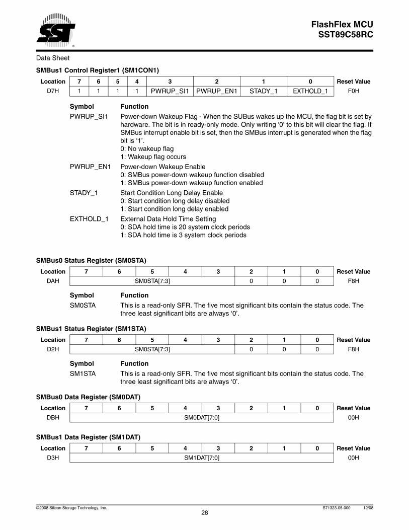
Symbol Function
PWRUP_SI1 Power-down Wakeup Flag - When the SUBus wakes up the MCU, the flag bit is set by hardware. The bit is in ready-only mode. Only writing ‘0’ to this bit will clear the flag. If SMBus interrupt enable bit is set, then the SMBus interrupt is generated when the flag bit is ‘1’.0: No wakeup flag1: Wakeup flag occurs
PWRUP_EN1 Power-down Wakeup Enable0: SMBus power-down wakeup function disabled1: SMBus power-down wakeup function enabled
STADY_1 Start Condition Long Delay Enable0: Start condition long delay disabled1: Start condition long delay enabled
EXTHOLD_1 External Data Hold Time Setting0: SDA hold time is 20 system clock periods1: SDA hold time is 3 system clock periods
Symbol Function
SM0STA This is a read-only SFR. The five most significant bits contain the status code. The three least significant bits are always ‘0’.
Symbol Function
SM1STA This is a read-only SFR. The five most significant bits contain the status code. The three least significant bits are always ‘0’.
SMBus1 Control Register1 (SM1CON1)
Location 7 6 5 4 3 2 1 0 Reset Value
D7H 1 1 1 1 PWRUP_SI1 PWRUP_EN1 STADY_1 EXTHOLD_1 F0H
SMBus0 Status Register (SM0STA)
Location 7 6 5 4 3 2 1 0 Reset Value
DAH SM0STA[7:3] 0 0 0 F8H
SMBus1 Status Register (SM1STA)
Location 7 6 5 4 3 2 1 0 Reset Value
D2H SM0STA[7:3] 0 0 0 F8H
SMBus0 Data Register (SM0DAT)
Location 7 6 5 4 3 2 1 0 Reset Value
DBH SM0DAT[7:0] 00H
SMBus1 Data Register (SM1DAT)
Location 7 6 5 4 3 2 1 0 Reset Value
D3H SM1DAT[7:0] 00H
28©2008 Silicon Storage Technology, Inc. S71323-05-000 12/08
Data Sheet
FlashFlex MCUSST89C58RC
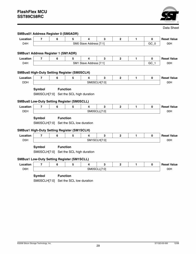
Symbol Function
SM0SCLH[7:0] Set the SCL high duration
Symbol Function
SM0SCLH[7:0] Set the SCL low duration
Symbol Function
SM0SCLH[7:0] Set the SCL high duration
Symbol Function
SM0SCLH[7:0] Set the SCL low duration
SMBus01 Address Register 0 (SM0ADR)
Location 7 6 5 4 3 2 1 0 Reset Value
D4H SM0 Slave Address [7:1] GC_0 00H
SMBus1 Address Register 1 (SM1ADR)
Location 7 6 5 4 3 2 1 0 Reset Value
D4H SM1 Slave Address [7:1] GC_1 00H
SMBus0 High-Duty Setting Register (SM0SCLH)
Location 7 6 5 4 3 2 1 0 Reset Value
DDH SM0SCLH[7:0] 00H
SMBus0 Low-Duty Setting Register (SM0SCLL)
Location 7 6 5 4 3 2 1 0 Reset Value
DEH SM0SCLL[7:0] 00H
SMBus1 High-Duty Setting Register (SM1SCLH)
Location 7 6 5 4 3 2 1 0 Reset Value
D5H SM1SCLH[7:0] 00H
SMBus1 Low-Duty Setting Register (SM1SCLL)
Location 7 6 5 4 3 2 1 0 Reset Value
D6H SM0SCLL[7:0] 00H
29©2008 Silicon Storage Technology, Inc. S71323-05-000 12/08
Data Sheet
FlashFlex MCUSST89C58RC
Symbol Function
SMOD1 Double Baud rate bit. If SMOD1 = 1, Timer 1 is used to generate the baud rate, and the serial port is used in modes 1, 2, and 3.
SMOD0 FE/SM0 Selection bit.0: SCON[7] = SM01: SCON[7] = FE,
POF Power-on reset status bit, this bit will not be affected by any other reset. POF should be cleared by software.0: No Power-on reset.1: Power-on reset occurred
GF1 General-purpose flag bit.
GF0 General-purpose flag bit.
PD Power-down bit, this bit is cleared by hardware after exiting from power-down mode.0: Power-down mode is not activated.1: Activates Power-down mode.
IDL Idle mode bit, this bit is cleared by hardware after exiting from idle mode.0: Idle mode is not activated.1: Activates idle mode.
Power Control Register (PCON)
Location 7 6 5 4 3 2 1 0 Reset Value
87H SMOD1 SMOD0 - POF GF1 GF0 PD IDL 00x10000b
30©2008 Silicon Storage Technology, Inc. S71323-05-000 12/08
Data Sheet
FlashFlex MCUSST89C58RC
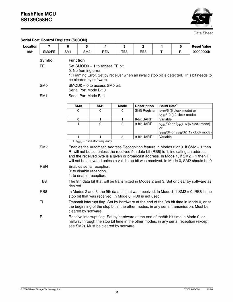
Symbol Function
FE Set SMOD0 = 1 to access FE bit.0: No framing error1: Framing Error. Set by receiver when an invalid stop bit is detected. This bit needs to be cleared by software.
SM0 SMOD0 = 0 to access SM0 bit.Serial Port Mode Bit 0
SM1 Serial Port Mode Bit 1
SM2 Enables the Automatic Address Recognition feature in Modes 2 or 3. If SM2 = 1 then RI will not be set unless the received 9th data bit (RB8) is 1, indicating an address, and the received byte is a given or broadcast address. In Mode 1, if SM2 = 1 then RI will not be activated unless a valid stop bit was received. In Mode 0, SM2 should be 0.
REN Enables serial reception.0: to disable reception.1: to enable reception.
TB8 The 9th data bit that will be transmitted in Modes 2 and 3. Set or clear by software as desired.
RB8 In Modes 2 and 3, the 9th data bit that was received. In Mode 1, if SM2 = 0, RB8 is the stop bit that was received. In Mode 0, RB8 is not used.
TI Transmit interrupt flag. Set by hardware at the end of the 8th bit time in Mode 0, or at the beginning of the stop bit in the other modes, in any serial transmission, Must be cleared by software.
RI Receive interrupt flag. Set by hardware at the end of the8th bit time in Mode 0, or halfway through the stop bit time in the other modes, in any serial reception (except see SM2). Must be cleared by software.
Serial Port Control Register (S0CON)
Location 7 6 5 4 3 2 1 0 Reset Value
98H SM0/FE SM1 SM2 REN TB8 RB8 TI RI 00000000b
SM0 SM1 Mode Description Baud Rate1
1. fOSC = oscillator frequency
0 0 0 Shift Register fOSC/6 (6 clock mode) or fOSC/12 (12 clock mode)
0 1 1 8-bit UART Variable1 0 2 9-bit UART fOSC/32 or fOSC/16 (6 clock mode)
or fOSC/64 or fOSC/32 (12 clock mode)
1 1 3 9-bit UART Variable
31©2008 Silicon Storage Technology, Inc. S71323-05-000 12/08
Data Sheet
FlashFlex MCUSST89C58RC
Symbol Function
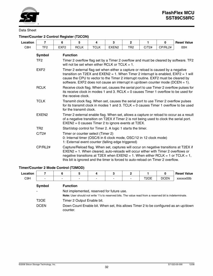
TF2 Timer 2 overflow flag set by a Timer 2 overflow and must be cleared by software. TF2 will not be set when either RCLK or TCLK = 1.
EXF2 Timer 2 external flag set when either a capture or reload is caused by a negative transition on T2EX and EXEN2 = 1. When Timer 2 interrupt is enabled, EXF2 = 1 will cause the CPU to vector to the Timer 2 interrupt routine. EXF2 must be cleared by software. EXF2 does not cause an interrupt in up/down counter mode (DCEN = 1).
RCLK Receive clock flag. When set, causes the serial port to use Timer 2 overflow pulses for its receive clock in modes 1 and 3. RCLK = 0 causes Timer 1 overflow to be used for the receive clock.
TCLK Transmit clock flag. When set, causes the serial port to use Timer 2 overflow pulses for its transmit clock in modes 1 and 3. TCLK = 0 causes Timer 1 overflow to be used for the transmit clock.
EXEN2 Timer 2 external enable flag. When set, allows a capture or reload to occur as a result of a negative transition on T2EX if Timer 2 is not being used to clock the serial port. EXEN2 = 0 causes Timer 2 to ignore events at T2EX.
TR2 Start/stop control for Timer 2. A logic 1 starts the timer.
C/T2# Timer or counter select (Timer 2)0: Internal timer (OSC/6 in 6 clock mode, OSC/12 in 12 clock mode)1: External event counter (falling edge triggered)
CP/RL2# Capture/Reload flag. When set, captures will occur on negative transitions at T2EX if EXEN2 = 1. When cleared, auto-reloads will occur either with Timer 2 overflows or negative transitions at T2EX when EXEN2 = 1. When either RCLK = 1 or TCLK = 1, this bit is ignored and the timer is forced to auto-reload on Timer 2 overflow.
Symbol Function
- Not implemented, reserved for future use.Note: User should not write ‘1’s to reserved bits. The value read from a reserved bit is indeterminate.
T2OE Timer 2 Output Enable bit.
DCEN Down Count Enable bit. When set, this allows Timer 2 to be configured as an up/down counter.
Timer/Counter 2 Control Register (T2CON)
Location 7 6 5 4 3 2 1 0 Reset Value
C8H TF2 EXF2 RCLK TCLK EXEN2 TR2 C/T2# CP/RL2# 00H
Timer/Counter 2 Mode Control (T2MOD)
Location 7 6 5 4 3 2 1 0 Reset Value
C9H - - - - - - T2OE DCEN xxxxxx00b
32©2008 Silicon Storage Technology, Inc. S71323-05-000 12/08
Data Sheet
FlashFlex MCUSST89C58RC
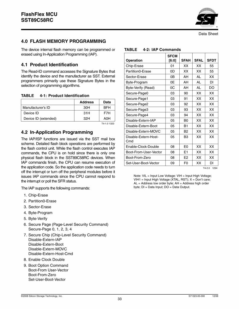
4.0 FLASH MEMORY PROGRAMMING
The device internal flash memory can be programmed orerased using In-Application Programming (IAP).
4.1 Product IdentificationThe Read-ID command accesses the Signature Bytes thatidentify the device and the manufacturer as SST. Externalprogrammers primarily use these Signature Bytes in theselection of programming algorithms.
4.2 In-Application ProgrammingThe IAP/ISP functions are issued via the SST mail boxscheme. Detailed flash block operations are performed bythe flash control unit. While the flash control executes IAPcommands, the CPU is on hold since there is only onephysical flash block in the SST89C58RC devices. WhenIAP commands finish, the CPU can resume execution ofthe application code. So the application code needs to turnoff the interrupt or turn off the peripheral modules before itissues IAP commands since the CPU cannot respond tothe interrupt or poll the SFR status.
The IAP supports the following commands:
1. Chip-Erase
2. Partition0-Erase
3. Sector-Erase
4. Byte-Program
5. Byte-Verify
6. Secure Page (Page-Level Security Command)Secure-Page 0, 1, 2, 3, 4
7. Secure Chip (Chip-Level Security Command)Disable-Extern-IAPDisable-Extern-BootDisable-Extern-MOVCDisable-Extern-Host-Cmd
8. Enable Clock Double
9. Boot Option CommandBoot-From User-VectorBoot-From-ZeroSet-User-Boot-Vector
Note: VIL = Input Low Voltage: VIH = Input High Voltage; VIH1 = Input High Voltage (XTAL, RST); X = Don’t care; AL = Address low order byte; AH = Address high order byte; DI = Data Input; DO = Data Output.
TABLE 4-1: Product Identification
Address Data
Manufacturer’s ID 30H BFH
Device ID 31H F7H
Device ID (extended) 32H A0HT4-1.0 1323
TABLE 4-2: IAP Commands
OperationSFCM[6:0] SFAH SFAL SFDT
Chip-Erase 01 XX XX 55
Partition0-Erase 0D XX XX 55
Sector-Erase 0B AH AL XX
Byte-Program 0E AH AL DI
Byte-Verify (Read) 0C AH AL DO
Secure-Page0 03 90 XX XX
Secure-Page1 03 91 XX XX
Secure-Page2 03 92 XX XX
Secure-Page3 03 93 XX XX
Secure-Page4 03 94 XX XX
Disable-Extern-IAP 05 B0 XX XX
Disable-Extern-Boot 05 B1 XX XX
Disable-Extern-MOVC 05 B2 XX XX
Disable-Extern-Host-Cmd
05 B3 XX XX
Enable-Clock-Double 08 E0 XX XX
Boot-From-User-Vector 08 E1 XX XX
Boot-From-Zero 08 E2 XX XX
Set-User-Boot-Vector 09 F0 XX DIT4-2.0 1294
33©2008 Silicon Storage Technology, Inc. S71323-05-000 12/08
Data Sheet
FlashFlex MCUSST89C58RC
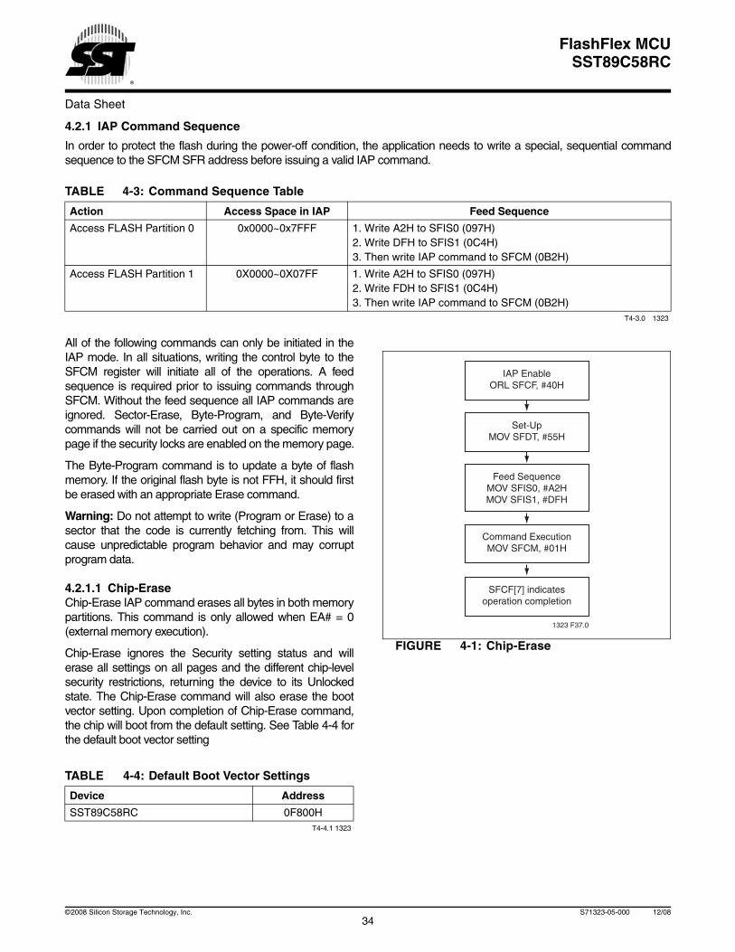
4.2.1 IAP Command Sequence
In order to protect the flash during the power-off condition, the application needs to write a special, sequential commandsequence to the SFCM SFR address before issuing a valid IAP command.
All of the following commands can only be initiated in theIAP mode. In all situations, writing the control byte to theSFCM register will initiate all of the operations. A feedsequence is required prior to issuing commands throughSFCM. Without the feed sequence all IAP commands areignored. Sector-Erase, Byte-Program, and Byte-Verifycommands will not be carried out on a specific memorypage if the security locks are enabled on the memory page.
The Byte-Program command is to update a byte of flashmemory. If the original flash byte is not FFH, it should firstbe erased with an appropriate Erase command.
Warning: Do not attempt to write (Program or Erase) to asector that the code is currently fetching from. This willcause unpredictable program behavior and may corruptprogram data.
4.2.1.1 Chip-EraseChip-Erase IAP command erases all bytes in both memorypartitions. This command is only allowed when EA# = 0(external memory execution).
Chip-Erase ignores the Security setting status and willerase all settings on all pages and the different chip-levelsecurity restrictions, returning the device to its Unlockedstate. The Chip-Erase command will also erase the bootvector setting. Upon completion of Chip-Erase command,the chip will boot from the default setting. See Table 4-4 forthe default boot vector setting
FIGURE 4-1: Chip-Erase
TABLE 4-3: Command Sequence Table
Action Access Space in IAP Feed Sequence
Access FLASH Partition 0 0x0000~0x7FFF 1. Write A2H to SFIS0 (097H)2. Write DFH to SFIS1 (0C4H)3. Then write IAP command to SFCM (0B2H)
Access FLASH Partition 1 0X0000~0X07FF 1. Write A2H to SFIS0 (097H)2. Write FDH to SFIS1 (0C4H)3. Then write IAP command to SFCM (0B2H)
T4-3.0 1323
TABLE 4-4: Default Boot Vector Settings
Device Address
SST89C58RC 0F800HT4-4.1 1323
Set-UpMOV SFDT, #55H
Feed SequenceMOV SFIS0, #A2HMOV SFIS1, #DFH
Command ExecutionMOV SFCM, #01H
SFCF[7] indicatesoperation completion
IAP EnableORL SFCF, #40H
1323 F37.0
34©2008 Silicon Storage Technology, Inc. S71323-05-000 12/08
Data Sheet
FlashFlex MCUSST89C58RC
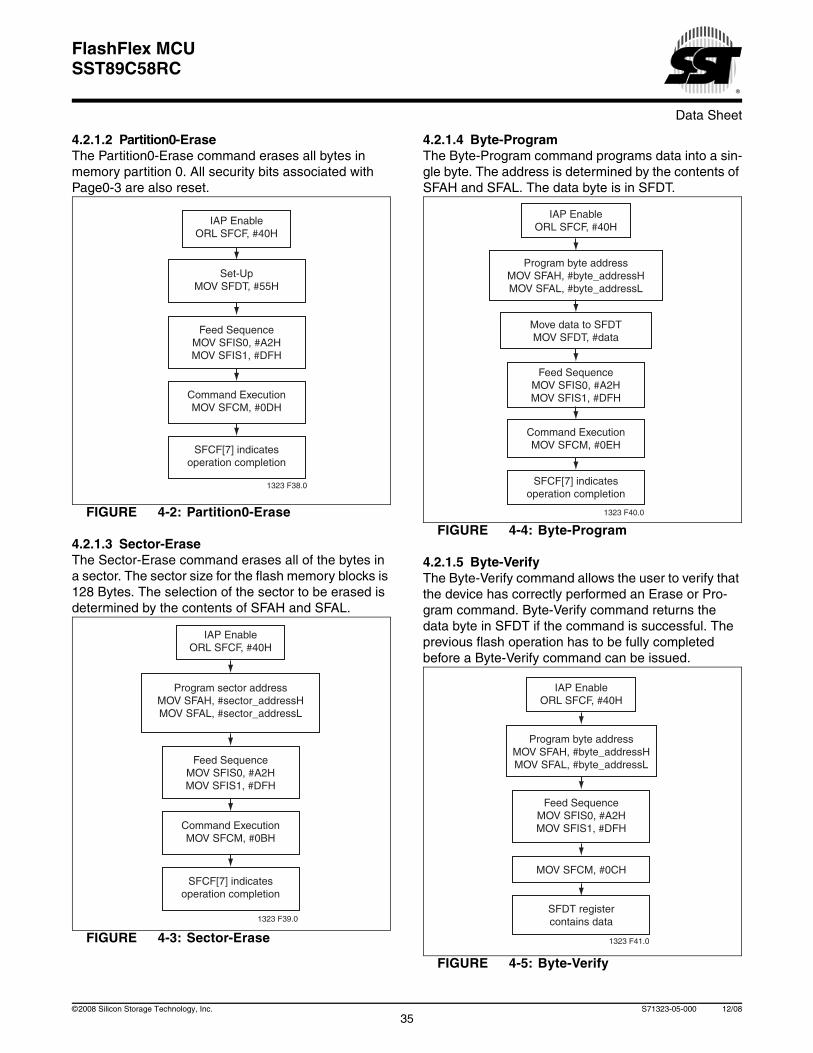
4.2.1.2 Partition0-EraseThe Partition0-Erase command erases all bytes in memory partition 0. All security bits associated with Page0-3 are also reset.
FIGURE 4-2: Partition0-Erase
4.2.1.3 Sector-EraseThe Sector-Erase command erases all of the bytes in a sector. The sector size for the flash memory blocks is 128 Bytes. The selection of the sector to be erased is determined by the contents of SFAH and SFAL.
FIGURE 4-3: Sector-Erase
4.2.1.4 Byte-ProgramThe Byte-Program command programs data into a sin-gle byte. The address is determined by the contents of SFAH and SFAL. The data byte is in SFDT.
FIGURE 4-4: Byte-Program
4.2.1.5 Byte-VerifyThe Byte-Verify command allows the user to verify that the device has correctly performed an Erase or Pro-gram command. Byte-Verify command returns the data byte in SFDT if the command is successful. The previous flash operation has to be fully completed before a Byte-Verify command can be issued.
FIGURE 4-5: Byte-Verify
Set-UpMOV SFDT, #55H
IAP EnableORL SFCF, #40H
Command ExecutionMOV SFCM, #0DH
SFCF[7] indicatesoperation completion
1323 F38.0
Feed SequenceMOV SFIS0, #A2HMOV SFIS1, #DFH
Program sector addressMOV SFAH, #sector_addressHMOV SFAL, #sector_addressL
Command ExecutionMOV SFCM, #0BH
SFCF[7] indicatesoperation completion
1323 F39.0
IAP EnableORL SFCF, #40H
Feed SequenceMOV SFIS0, #A2HMOV SFIS1, #DFH
Move data to SFDTMOV SFDT, #data
Command ExecutionMOV SFCM, #0EH
SFCF[7] indicatesoperation completion
Program byte addressMOV SFAH, #byte_addressHMOV SFAL, #byte_addressL
1323 F40.0
IAP EnableORL SFCF, #40H
Feed SequenceMOV SFIS0, #A2HMOV SFIS1, #DFH
MOV SFCM, #0CH
SFDT registercontains data
Program byte addressMOV SFAH, #byte_addressHMOV SFAL, #byte_addressL
1323 F41.0
IAP EnableORL SFCF, #40H
Feed SequenceMOV SFIS0, #A2HMOV SFIS1, #DFH
35©2008 Silicon Storage Technology, Inc. S71323-05-000 12/08
Data Sheet
FlashFlex MCUSST89C58RC
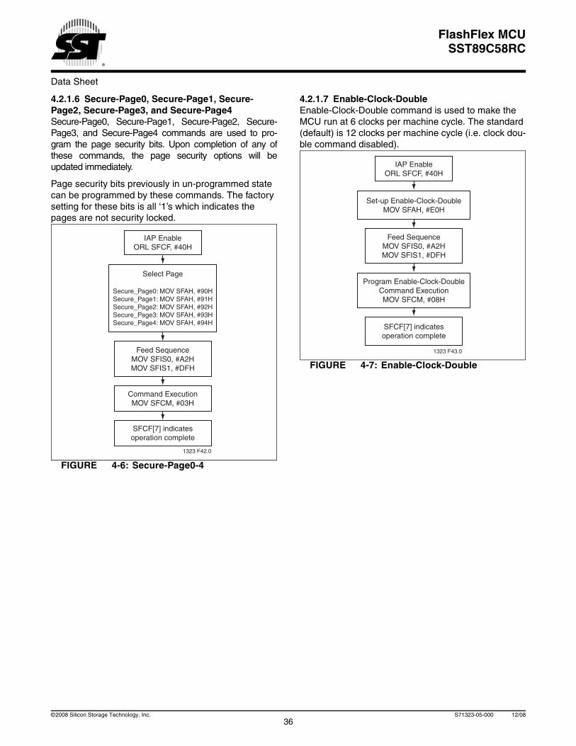
4.2.1.6 Secure-Page0, Secure-Page1, Secure-Page2, Secure-Page3, and Secure-Page4Secure-Page0, Secure-Page1, Secure-Page2, Secure-Page3, and Secure-Page4 commands are used to pro-gram the page security bits. Upon completion of any ofthese commands, the page security options will beupdated immediately.
Page security bits previously in un-programmed state can be programmed by these commands. The factory setting for these bits is all ‘1’s which indicates the pages are not security locked.
FIGURE 4-6: Secure-Page0-4
4.2.1.7 Enable-Clock-DoubleEnable-Clock-Double command is used to make the MCU run at 6 clocks per machine cycle. The standard (default) is 12 clocks per machine cycle (i.e. clock dou-ble command disabled).
FIGURE 4-7: Enable-Clock-Double
Select Page
Secure_Page0: MOV SFAH, #90HSecure_Page1: MOV SFAH, #91HSecure_Page2: MOV SFAH, #92HSecure_Page3: MOV SFAH, #93HSecure_Page4: MOV SFAH, #94H
SFCF[7] indicatesoperation complete
Command ExecutionMOV SFCM, #03H
1323 F42.0
IAP EnableORL SFCF, #40H
Feed SequenceMOV SFIS0, #A2HMOV SFIS1, #DFH
Program Enable-Clock-DoubleCommand ExecutionMOV SFCM, #08H
SFCF[7] indicatesoperation complete
1323 F43.0
IAP EnableORL SFCF, #40H
Set-up Enable-Clock-DoubleMOV SFAH, #E0H
Feed SequenceMOV SFIS0, #A2HMOV SFIS1, #DFH
36©2008 Silicon Storage Technology, Inc. S71323-05-000 12/08
Data Sheet
FlashFlex MCUSST89C58RC
4.3 In-System ProgrammingThe bootstrap loader (BSL) is located in partition 1 andcannot be accessed unless the SFR AUXR1 (Address =A2H), Bit 5 is enabled. The default value of this bit afterreset is ‘1’ unless the “Boot-From-Zero” bit is non-zero dur-ing reset, or P1.0 and P1.1 are pulled low while EA# is heldhigh on the falling edge of the reset.
4.3.1 Normal Mode
If the “Boot-From-Zero” bit is ‘0’, the MCU boots from0x0000. If both the “Boot-From-Zero” bit and the “Boot-From-User-Vector” bit are ‘1’, the USER Boot Vector isapplicable (0xF800).
If the “Boot-From-Zero” bit is ‘1’ and the “Boot-From-User-Vector” bit is ‘0’, the USER Boot Vector is applicable. This isused as the high byte of the program counter (PC) startingaddress while the lower byte of PC is 00H. See Figure 4-8.
FIGURE 4-8: Boot Sequence Flowchart
1337 F61.1
Power-on
External Boot (EA)?
Default Boot Vector0x0000
No
Hardware ActiveBoth P1.0, P1.1
are Low
No
External ROM0x0000
“Boot-From-Zero”Bit = 0?
No
“Boot-From-User-Vector” = 0?
No
Yes
Yes
User Boot Vector
Yes
37©2008 Silicon Storage Technology, Inc. S71323-05-000 12/08
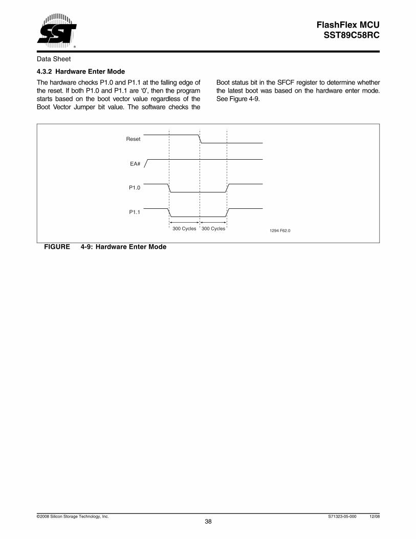
Data Sheet
FlashFlex MCUSST89C58RC
4.3.2 Hardware Enter Mode
The hardware checks P1.0 and P1.1 at the falling edge ofthe reset. If both P1.0 and P1.1 are ‘0’, then the programstarts based on the boot vector value regardless of theBoot Vector Jumper bit value. The software checks the
Boot status bit in the SFCF register to determine whetherthe latest boot was based on the hardware enter mode.See Figure 4-9.
FIGURE 4-9: Hardware Enter Mode
300 Cycles
EA#
Reset
1294 F62.0300 Cycles
P1.1
P1.0
38©2008 Silicon Storage Technology, Inc. S71323-05-000 12/08
Data Sheet
FlashFlex MCUSST89C58RC
5.0 TIMERS/COUNTERS
5.1 TimersThe device has three 16-bit registers that can be used aseither timers or event counters. The three timers/countersare denoted Timer 0 (T0), Timer 1 (T1), and Timer 2 (T2).Each is designated a pair of 8-bit registers in the SFRs.The pair consists of a most significant (high) byte and leastsignificant (low) byte. The respective registers are TL0,TH0, TL1, TH1, TL2, and TH2.
5.2 Timer Set-upRefer to Table 3-6 for TMOD, TCON, and T2CON registersregarding timers T0, T1, and T2. The following tables pro-vide TMOD values to be used to set up Timers T0, T1, andT2.
Except for the baud rate generator mode, the values givenfor T2CON do not include the setting of the TR2 bit. There-fore, bit TR2 must be set separately to turn the timer on.
TABLE 5-1: Timer/Counter 0
Mode Function
TMOD
InternalControl1
1. The Timer is turned ON/OFF by setting/clearing bit TR0 in the software.
ExternalControl2
2. The Timer is turned ON/OFF by the 1 to 0 transition on INT0# (P3.2) when TR0 = 1 (hardware control).
Used asTimer
0 13-bit Timer 00H 08H
1 16-bit Timer 01H 09H
2 8-bit Auto-Reload 02H 0AH
3 Two 8-bit Timers 03H 0BH
Used asCounter
0 13-bit Timer 04H 0CH
1 16-bit Timer 05H 0DH
2 8-bit Auto-Reload 06H 0EH
3 Two 8-bit Timers 07H 0FHT5-1.0 1323
TABLE 5-2: Timer/Counter 1
Mode Function
TMOD
InternalControl1
ExternalControl2
Used asTimer
0 13-bit Timer 00H 80H
1 16-bit Timer 10H 90H
2 8-bit Auto-Reload 20H A0H
3 Does not run 30H B0H
Used asCounter
0 13-bit Timer 40H C0H
1 16-bit Timer 50H D0H
2 8-bit Auto-Reload 60H E0H
3 Not available - -T5-2.0 1323
1. The Timer is turned ON/OFF by setting/clearing bit TR1 in the software.
2. The Timer is turned ON/OFF by the 1 to 0 transition on INT1# (P3.3) when TR1 = 1 (hardware control).
TABLE 5-3: Timer/Counter 2
Mode
T2CON
InternalControl1
1. Capture/Reload occurs only on timer/counter overflow.
ExternalControl2
2. Capture/Reload occurs on timer/counter overflow and a 1 to 0 transition on T2EX (P1.1) pin except when Timer 2 is used in the baud rate generating mode.
Used asTimer
16-bit Auto-Reload 00H 08H
16-bit Capture 01H 09H
Baud rate generatorreceive and transmit
same baud rate
34H 36H
Receive only 24H 26H
Transmit only 14H 16H
Used asCounter
16-bit Auto-Reload 02H 0AH
16-bit Capture 03H 0BHT5-3.0 1323
39©2008 Silicon Storage Technology, Inc. S71323-05-000 12/08

Data Sheet
FlashFlex MCUSST89C58RC
5.3 Programmable Clock-OutA 50% duty cycle clock can be programmed to come outon P1.0. This pin, besides being a regular I/O pin, has twoalternate functions. It can be programmed:
1. to input the external clock for Timer/Counter 2, or
2. to output a 50% duty cycle clock ranging from 122 Hz to 8 MHz at a 16 MHz operating frequency (61 Hz to 4 MHz in 12 clock mode).
To configure Timer/Counter 2 as a clock generator, bitC/#T2 (in T2CON) must be cleared and bit T20E inT2MOD must be set. Bit TR2 (T2CON.2) also must be setto start the timer.
The Clock-Out frequency depends on the oscillator fre-quency and the reload value of Timer 2 capture registers(RCAP2H, RCAP2L) as shown in this equation:
Oscillator Frequencyn x (65536 - RCAP2H, RCAP2L)
n = 2 (in 6 clock mode)4 (in 12 clock mode)
Where (RCAP2H, RCAP2L) = the contents of RCAP2Hand RCAP2L taken as a 16-bit unsigned integer.
In the Clock-Out mode, Timer 2 roll-overs will not generatean interrupt. This is similar to when it is used as a baud-rategenerator. It is possible to use Timer 2 as a baud-rate gen-erator and a clock generator simultaneously. Note, how-ever, that the baud-rate and the Clock-Out frequency willnot be the same.
6.0 SERIAL I/O
6.1 Full-Duplex, Enhanced UARTThe device serial I/O port is a full-duplex port that allowsdata to be transmitted and received simultaneously inhardware by the transmit and receive registers, respec-tively, while the software is performing other tasks. Thetransmit and receive registers are both located in theSerial Data Buffer (SBUF) special function register. Writ-ing to the SBUF register loads the transmit register, andreading from the SBUF register obtains the contents ofthe receive register.
The UART has four modes of operation which are selectedby the Serial Port Mode Specifier (SM0 and SM1) bits ofthe Serial Port Control (SCON) special function register. Inall four modes, transmission is initiated by any instructionthat uses the SBUF register as a destination register.Reception is initiated in mode 0 when the Receive Interrupt(RI) flag bit of the Serial Port Control (SCON) SFR iscleared and the Reception Enable/ Disable (REN) bit of theSCON register is set. Reception is initiated in the othermodes by the incoming start bit if the REN bit of the SCONregister is set.
6.1.1 Framing Error Detection
Framing Error Detection is a feature, which allows thereceiving controller to check for valid stop bits in modes 1,2, or 3. Missing stops bits can be caused by noise in seriallines or from simultaneous transmission by two CPUs.
Framing Error Detection is selected by going to the PCONregister and changing SMOD0 = 1 (see Figure 6-1). If astop bit is missing, the Framing Error bit (FE) will be set.Software may examine the FE bit after each reception tocheck for data errors. After the FE bit has been set, it canonly be cleared by software. Valid stop bits do not clear FE.When FE is enabled, RI rises on the stop bit, instead of thelast data bit (see Figure 6-2 and Figure 6-3).
40©2008 Silicon Storage Technology, Inc. S71323-05-000 12/08
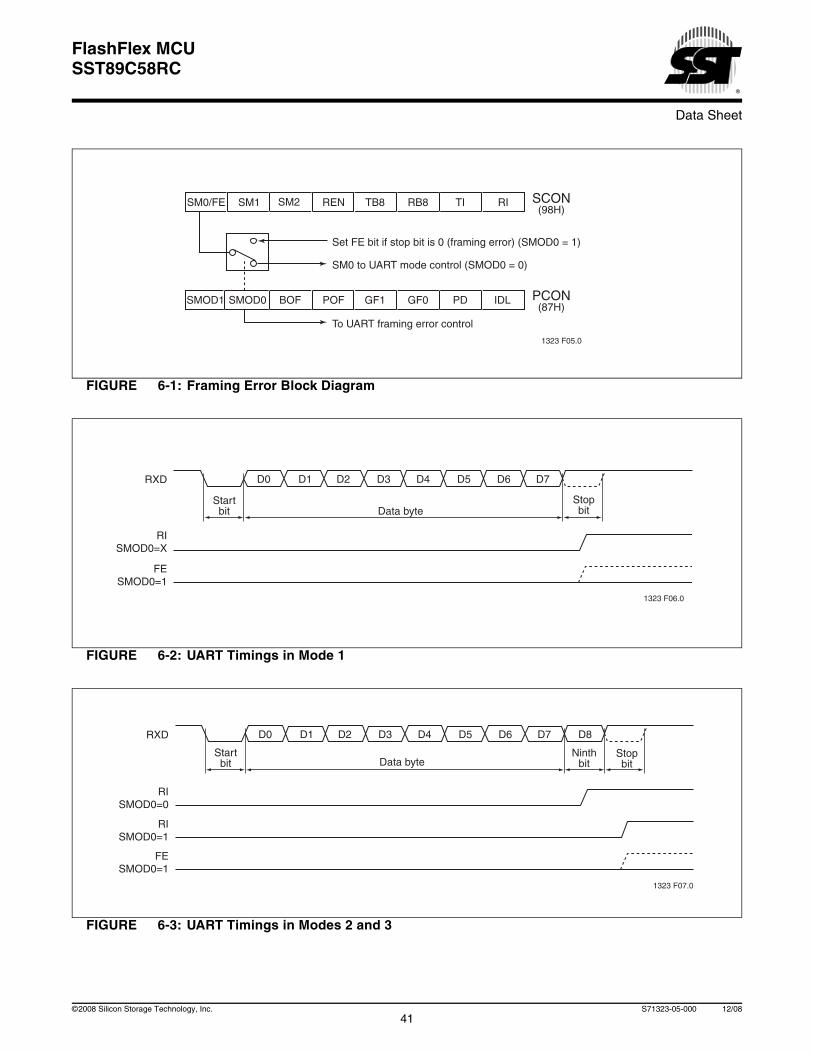
Data Sheet
FlashFlex MCUSST89C58RC
FIGURE 6-1: Framing Error Block Diagram
FIGURE 6-2: UART Timings in Mode 1
FIGURE 6-3: UART Timings in Modes 2 and 3
1323 F05.0
SM0/FE SM1 SM2 REN TB8 RB8 TI RI
SMOD0SMOD1 POF GF1 GF0 PD IDL
SCON(98H)
PCON(87H)
Set FE bit if stop bit is 0 (framing error) (SMOD0 = 1)
SM0 to UART mode control (SMOD0 = 0)
To UART framing error control
BOF
Startbit
RXD
RISMOD0=X
FESMOD0=1
D0 D1 D2 D3 D4 D5 D6 D7
Data byteStopbit
1323 F06.0
Startbit
RXD
RISMOD0=1
FESMOD0=1
RISMOD0=0
D0 D1 D2 D3 D4 D5 D6 D7 D8
Data byteNinth
bitStopbit
1323 F07.0
41©2008 Silicon Storage Technology, Inc. S71323-05-000 12/08
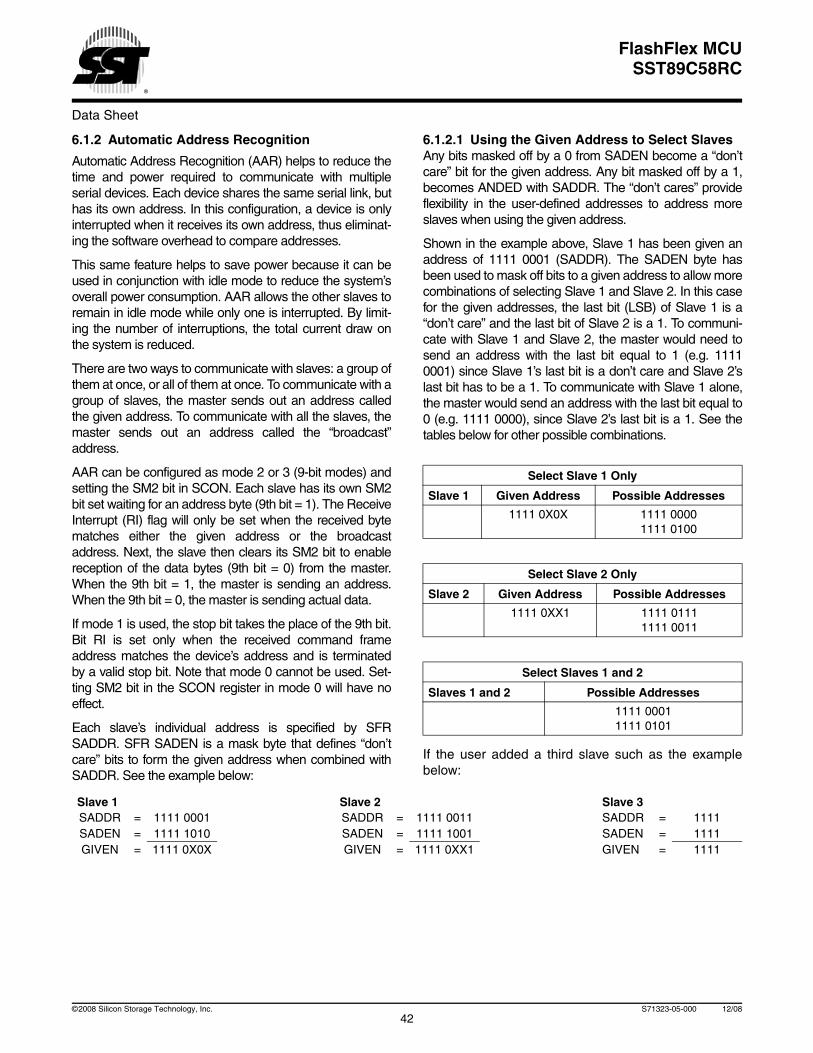
Data Sheet
FlashFlex MCUSST89C58RC
6.1.2 Automatic Address Recognition
Automatic Address Recognition (AAR) helps to reduce thetime and power required to communicate with multipleserial devices. Each device shares the same serial link, buthas its own address. In this configuration, a device is onlyinterrupted when it receives its own address, thus eliminat-ing the software overhead to compare addresses.
This same feature helps to save power because it can beused in conjunction with idle mode to reduce the system’soverall power consumption. AAR allows the other slaves toremain in idle mode while only one is interrupted. By limit-ing the number of interruptions, the total current draw onthe system is reduced.
There are two ways to communicate with slaves: a group ofthem at once, or all of them at once. To communicate with agroup of slaves, the master sends out an address calledthe given address. To communicate with all the slaves, themaster sends out an address called the “broadcast”address.
AAR can be configured as mode 2 or 3 (9-bit modes) andsetting the SM2 bit in SCON. Each slave has its own SM2bit set waiting for an address byte (9th bit = 1). The ReceiveInterrupt (RI) flag will only be set when the received bytematches either the given address or the broadcastaddress. Next, the slave then clears its SM2 bit to enablereception of the data bytes (9th bit = 0) from the master.When the 9th bit = 1, the master is sending an address.When the 9th bit = 0, the master is sending actual data.
If mode 1 is used, the stop bit takes the place of the 9th bit.Bit RI is set only when the received command frameaddress matches the device’s address and is terminatedby a valid stop bit. Note that mode 0 cannot be used. Set-ting SM2 bit in the SCON register in mode 0 will have noeffect.
Each slave’s individual address is specified by SFRSADDR. SFR SADEN is a mask byte that defines “don’tcare” bits to form the given address when combined withSADDR. See the example below:
6.1.2.1 Using the Given Address to Select SlavesAny bits masked off by a 0 from SADEN become a “don’tcare” bit for the given address. Any bit masked off by a 1,becomes ANDED with SADDR. The “don’t cares” provideflexibility in the user-defined addresses to address moreslaves when using the given address.
Shown in the example above, Slave 1 has been given anaddress of 1111 0001 (SADDR). The SADEN byte hasbeen used to mask off bits to a given address to allow morecombinations of selecting Slave 1 and Slave 2. In this casefor the given addresses, the last bit (LSB) of Slave 1 is a“don’t care” and the last bit of Slave 2 is a 1. To communi-cate with Slave 1 and Slave 2, the master would need tosend an address with the last bit equal to 1 (e.g. 11110001) since Slave 1’s last bit is a don’t care and Slave 2’slast bit has to be a 1. To communicate with Slave 1 alone,the master would send an address with the last bit equal to0 (e.g. 1111 0000), since Slave 2’s last bit is a 1. See thetables below for other possible combinations.
If the user added a third slave such as the examplebelow:
Select Slave 1 Only
Slave 1 Given Address Possible Addresses
1111 0X0X 1111 0000 1111 0100
Select Slave 2 Only
Slave 2 Given Address Possible Addresses
1111 0XX1 1111 01111111 0011
Select Slaves 1 and 2
Slaves 1 and 2 Possible Addresses
1111 0001 1111 0101
Slave 1 Slave 2 Slave 3SADDR = 1111 0001 SADDR = 1111 0011 SADDR = 1111SADEN = 1111 1010 SADEN = 1111 1001 SADEN = 1111GIVEN = 1111 0X0X GIVEN = 1111 0XX1 GIVEN = 1111
42©2008 Silicon Storage Technology, Inc. S71323-05-000 12/08
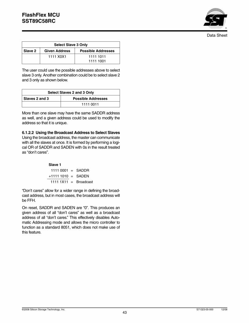
Data Sheet
FlashFlex MCUSST89C58RC
The user could use the possible addresses above to selectslave 3 only. Another combination could be to select slave 2and 3 only as shown below.
More than one slave may have the same SADDR addressas well, and a given address could be used to modify theaddress so that it is unique.
6.1.2.2 Using the Broadcast Address to Select SlavesUsing the broadcast address, the master can communicatewith all the slaves at once. It is formed by performing a logi-cal OR of SADDR and SADEN with 0s in the result treatedas “don’t cares”.
“Don’t cares” allow for a wider range in defining the broad-cast address, but in most cases, the broadcast address willbe FFH.
On reset, SADDR and SADEN are “0”. This produces angiven address of all “don’t cares” as well as a broadcastaddress of all “don’t cares.” This effectively disables Auto-matic Addressing mode and allows the micro controller tofunction as a standard 8051, which does not make use ofthis feature.
Select Slave 3 Only
Slave 2 Given Address Possible Addresses
1111 X0X1 1111 10111111 1001
Select Slaves 2 and 3 Only
Slaves 2 and 3 Possible Addresses
1111 0011
Slave 1
1111 0001 = SADDR
+1111 1010 = SADEN
1111 1X11 = Broadcast
43©2008 Silicon Storage Technology, Inc. S71323-05-000 12/08
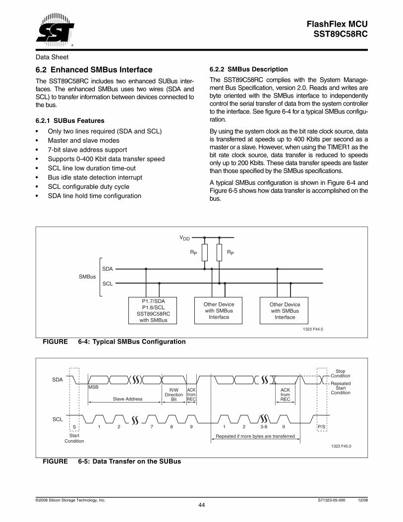
Data Sheet
FlashFlex MCUSST89C58RC
6.2 Enhanced SMBus InterfaceThe SST89C58RC includes two enhanced SUBus inter-faces. The enhanced SMBus uses two wires (SDA andSCL) to transfer information between devices connected tothe bus.
6.2.1 SUBus Features
• Only two lines required (SDA and SCL)• Master and slave modes• 7-bit slave address support• Supports 0-400 Kbit data transfer speed• SCL line low duration time-out• Bus idle state detection interrupt• SCL configurable duty cycle• SDA line hold time configuration
6.2.2 SMBus Description
The SST89C58RC complies with the System Manage-ment Bus Specification, version 2.0. Reads and writes arebyte oriented with the SMBus interface to independentlycontrol the serial transfer of data from the system controllerto the interface. See figure 6-4 for a typical SMBus configu-ration.
By using the system clock as the bit rate clock source, datais transferred at speeds up to 400 Kbits per second as amaster or a slave. However, when using the TIMER1 as thebit rate clock source, data transfer is reduced to speedsonly up to 200 Kbits. These data transfer speeds are fasterthan those specified by the SMBus specifications.
A typical SMBus configuration is shown in Figure 6-4 andFigure 6-5 shows how data transfer is accomplished on thebus.
FIGURE 6-4: Typical SMBus Configuration
FIGURE 6-5: Data Transfer on the SUBus
1323 F44.0
P1.7/SDAP1.6/SCL
SST89C58RCwith SMBus
Other Devicewith SMBus
Interface
RPRP
VDD
SMBus
SDA
SCL
Other Devicewith SMBus
Interface
StartCondition
SDA
StopCondition
1323 F45.0
SCL93-82121 987 P/S
RepeatedStart
ConditionACKfromREC
ACKfromREC
MSB
Slave Address
S
R/WDirection
Bit
Repeated if more bytes are transferred
44©2008 Silicon Storage Technology, Inc. S71323-05-000 12/08

Data Sheet
FlashFlex MCUSST89C58RC
6.2.2.1 SDA (Serial Data Line)The SDA line is the SMBus serial data line, and is primarilydriven by the master or slave transmitter. The SDA ischangeable when SCL is low, and SDA is stable when SCLis high. Perform bus arbitration on SDA when SCL is high.
6.2.2.2 SCL (Serial Clock Line)The SCL line is the SMBus serial clock line which providessynchronized transmissions between master and slavedevices and is driven by the master devices. When multiplemasters drive the SCL simultaneously, a wired-AND com-bines all signals into one synchronized clock signal. Theslowest clock determines the synchronized LOW periodand the fastest clock determines the HIGH period.
6.2.3 SMBus Modes of Operation
The SMBus transaction begins with a START which is fol-lowed by an address byte and data, and then ends with aSTOP. An acknowledge bit from the receiver follows theaddress byte, which consists of a 7-bit address plus adirection bit, and each data byte. The direction bit (R/W),which occupies the least significant bit position of theaddress, indicates a READ operation when set to logic ‘1’,and a WRITE operation when set to logic ‘0’. The mastercan address multiple slaves simultaneously using a generalcall address (0x00 + R/W), which is recognized by all slavedevices.
The master initiates all transactions with one or more tar-get-addressed slave devices. After generating a STARTcondition, the master transmits the address and directionbit. For a master-to-slave WRITE operation, data is trans-mitted a byte at a time from the master; waiting for anacknowledge after each byte from the slave. For a slave-to-master READ operation, the slave awaits an acknowledgeafter each byte from the master. The master generates aSTOP which ends the transaction and frees the bus at thecompletion of the data transfer.
At any time, the SMBus is configured to operate in eithermaster or slave mode.
6.2.3.1 Master Transmitter ModeThe serial data is output through SDA while SCL suppliesthe serial clock. The first transmitted byte contains the slaveaddress and the data direction bit. In this WRITE operationmode, the data direction bit (R/W) will be logic ‘0’ and themaster transmits serial data. After each byte is transmitted,an acknowledge bit is received from the slave. START andSTOP conditions are output by the master to indicate thebeginning and the end of a serial transfer.
6.2.3.2 Master Receiver ModeThe serial data is received via SDA while SCL supplies theserial clock. The first master-transmitted byte contains theslave address and the data direction bit. In this READmode, the data direction bit (R/W) will be logic ‘1’. Serialdata is received from the slave via SDA while SCL outputsthe serial clock from the master. After each byte is receivedfrom the slave, an acknowledge bit is transmitted by themaster. START and STOP conditions are output to indicatethe beginning and end of a serial transfer.
6.2.3.3 Slave Receiver ModeThe serial data is output through SDA while SCL suppliesthe serial clock. The first transmitted byte contains anaddress and the data direction bit. In this READ mode, thedata direction bit (R/W) will be logic ‘1’. Serial data is trans-mitted to the master if the address received matches theslave’s assigned address or if a general call address isreceived. After each byte is received, an acknowledge bit istransmitted. START and STOP conditions are recognizedas the beginning and end of a serial transfer.
6.2.3.4 Slave Transmitter ModeThe serial data is received via SDA while SCL supplies theserial clock. The first transmitted byte contains an addressand the data direction bit. In this WRITE operation mode,the data direction bit (R/W) will be logic ‘0’. Serial data istransmitted to the master if the address received matchesthe slave’s assigned address or if a general call address isreceived. After each byte is received, an acknowledge bit istransmitted. START and STOP conditions are recognizedas the beginning and end of a serial transfer.
6.3 Timeouts
6.3.1 SCL Low Timeout
Use the TOE bit to enable monitoring of the SCL low time-out function. When the TOE is set, the SMBUS controls theTIMER1 to count during every SCL low period. At everyfalling-edge of the SCL, a reload counter pulse is gener-ated to TIMER1. At every rising-edge of the SCL, a countstop pulse is generated to TIMER1. If the TIMER1’scounter is reloaded and counting, the last count stop pulsewill cause the TIMER1 to generate an interrupt for SCL lowtimeout. 1 = SCL Low timeout enable0 = SCL Low timeout disabled
45©2008 Silicon Storage Technology, Inc. S71323-05-000 12/08

Data Sheet
FlashFlex MCUSST89C58RC
6.3.2 SCL High (SMBus Free) Timeout
According to SMBus specifications, the bus is designatedas free if the device holds the SCL and SDA lines high formore than 10 SMBus bit rate cycles.
6.4 SMBus SFRThe SST89C58RC has two identical SMBus interfaces,each identical with the exception of the SFR addresses andthe I/O pins associated with each interface.
The SMBus interfaces operate as a master and/or slaveand can function on a bus with multiple masters. TheSMBus controls the SDA, the generation and synchroniza-tion of the SCL, the arbitration logic, and the control andgeneration of START/STOP. The following SFRs are asso-ciated with the SMBus.
6.4.1 SMBus Control Register
SMBus control register SM0CON0 configures and controlsthe SMBus interface making all bits in the register softwarereadable and writable. The SMBus hardware sets theSerial Interrupt flag (SI_0, SMCON0.4) to logic ‘1’ when avalid serial interrupt condition occurs; and clears the Stopflag (STO_5, SM0CON0.4) to logic ‘0’ when a STOP condi-tion is present on the bus.
Enable the SMBus interface, by setting the SMBEN_0 flagto logic ‘1’; disable and remove it from the bus by clearingthe ENSMB flag to logic ‘0’. To reset the SMBus communi-cation, momentarily clear the SMBEN flag and then reset itto logic ‘1’. Using SMBEN to temporarily remove a devicefrom the bus will result in lost information. The best methodto temporarily remove a device from the bus is to use theAssert Acknowledge (AA) flag.
If the bus is idle, SMBus generates a START condition aftera delay of 1.5 baud rate clock cycle when the Start flag(STA_0, Sm0CON0.6) is set. If STA and STADY bits areboth set in the first transmission (that is, the SMBEN is setfrom “0” to “1”) and bus is idle, a START condition will begenerated after 10 baud rate clock cycles. If SMBUS isalready in the master mode and one or more than onebytes has been transmitted or received, a repeated STARTcondition will be generated when STA bit is set. If SMBus isin addressed slave mode and the STA is set, no STARTcondition will be generated until SMBus enters “notaddressed slave” mode and the bus is idle. STA bit onlycan be cleared by software.
In master mode, a STOP condition is transmitted on thebus when the Stop flag (STO_0, SM0CON0.5) is set. AndSTO bit is cleared by hardware automatically after a STOPcondition is detected on the bus. If STA and STO bits areboth set, the STOP condition is transmitted firstly, and thenthe START condition is transmitted.
In slave mode, STO is set to recover SMBus from an errorcondition or generate a internal STOP for a forced accessto the bus. No STOP condition will be transmitted on thebus and the hardware behaves as if a STOP condition hasbeen received, SMBUS switches to “not addressed” slavereceiver mode. STO bit is cleared by hardware after onesystem clocks. STO bit can not be set when SMBEN iszero.
The Serial Interrupt flag (SI_0, SM0CON0.4) can be set inany possible SMBus status except for status “0xD0” andstatus “0xF8. If EA and ES1 bits are set, an interrupt willrequested when SI is set. When SI flag is set by hardware,the SCL line is held to LOW until it is cleared by software(except for the status “0xD0”, which will not hold the SCLline low). Only “0” can be written to clear SI flag, writing “1”has no effect to the flag. When SI flag is cleared, SMBSTAregister changes to “0xF8”.
During the acknowledge clock cycle on the SCL line, theAssert Acknowledge flag (AA_0, SM0CON0.3) sets thelevel of the SDA line.
In slave transmitter mode, the AA flag is used to determinewhether the last data byte will be transmitted or enableswhether to respond its slave address or general calladdress.
In master receiver mode, the AA flag is used to determineto return ACK or NACK after receiving a byte. In slavereceiver mode, the AA flag is used to determine to returnACK or NACK and enables whether to respond its slaveaddress or general call address.
TABLE 6-1: SMBus SFR Functions
SFR Function
SM0CON0 / SM0CON1 Configures SMBus0
SM0STA Controls status of SMBus0
SM0DAT Data register for transmitting and receiving SMBus0 data
SM0ADR Indicates SMBus0 slave address
SM0SCLH / SM0SCLL Configures SMBus0 High/Low duty
SM1CON0 / SM1CON1 Configures SMBus1
SM1STA Controls status of SMBus1
SM1DAT Data register for transmitting and receiving SMBus1 data
SM1ADR Indicates SMBus1 slave address
SM1SCLH / SM1SCLL Configures SMBus1 High/Low dutyT6-1.1323
46©2008 Silicon Storage Technology, Inc. S71323-05-000 12/08
Data Sheet
FlashFlex MCUSST89C58RC
1 = When set to 1, an acknowledge (low level to SDA) will be returned during the acknowledge clock pulse on the SCL line on the following situations:
3. The “own slave address” has been received.
4. The general call address has been received while the general call bit (GC) in SMBADR is set.
5. A data byte has been received while the SMBUS interface is in the Master Receiver Mode.
6. A data byte has been received while the SMBUS interface is in the addressed Slave Receiver Mode.
0 = When cleared to 0, an non-acknowledge (high level to SDA) will be returned during the acknowledge clock pulse on the SCL line on the following situations:
1. A data byte has been received while the SMBUS interface is in the Master Receiver Mode.
2. A data byte has been received while the SMBUS interface is in the addressed Slave Receiver Mode.
To enable the SMBus Free Timeout feature, set the SMBusFree Timer Enable bit (FTE, SM0CON0.2) to logic ‘1’. Thebus is considered free and, if pending, a Start is generatedwhen SCL and SDA remain high for the SMBus Free Time-out given in the SMBUS Clock Rate Register.
To enable monitoring SCL low timeout function, set theSMBus Time out Enable bit (TOE_0, SM0CON0.1) to logic‘1’. When TOE is set, SMBUS will control the TIMER1 tocount during the every SCL low period. At every SCL fall-ing-edge of the SCL, a reload counter pulse is generated toTIMER1; at every SCL rising-edge of the SCL, a count stoppulse is generated to TIMER1. If the TIMER1’s counter isreloaded and counting, the latest count stop pulse willcause the TIMER1 to generate an interrupt for SCL lowtimeout.
6.4.2 Data Register
The SMBus Data register (SM0DAT0) holds a byte ofrecently received or ready-to-transmit serial data. When SIis set to logic ‘1’, the data in the register is stable. In thisstate, software safely reads or writes the data register.However, when the SMBus is enabled and the SI flag iscleared to logic ‘0’, the software must not access theSM0DAT register because the hardware may be shifting adata byte in or out of the register.
After the SM0DAT receives a byte of data, the first bit of theserial data byte is located at the MSB. As data is shifted outof the SM0DAT, beginning with the MSB, data from the busis simultaneously shifted in.
The last data byte on the bus is always contained in theSM0DAT; thereby, ensuring that correct data is transmittedfrom the master to the slave in the event of lost arbitration.
6.4.3 Address Register
The slave address is held in the SM0ADR Address regis-ter. When in slave mode, the 7-bit address is held in theseven most significant bits, the least of which is bit 0. Bit 0recognizes the general call address (0x00) when set tologic ‘1’. When the SMBus hardware is operating in mastermode, the contents of the SM0ADR Address register areignored.
6.4.4 Status Register
The status of the SMBus is held in the SM0STA Status reg-ister as one of 31 different 8-bit status codes. Each 8-bitstatus code corresponds to a unique SMBus state. WhenSI = ‘1’, the three least significant bits of the status code areset to zero and the five most significant bits vary. All possi-ble status codes are multiples of eight; which, in software,allows the status code to act as an index to branch to ser-vice routines by allowing 8 bytes of code to service thestate or jump to a more extensive routine.
Set the SI flag to logic ‘1’ to define the contents of theSM0STA register for software use. Software must not writeto the SM0STA because doing so yields uncertain results.Refer to Tables 6-1 through 6-4 for the 31 SMBus statesand their corresponding status codes.
47©2008 Silicon Storage Technology, Inc. S71323-05-000 12/08

Data Sheet
FlashFlex MCUSST89C58RC
TABLE 6-2: Master Transmitter Mode
Status Code
(SM0STA)SMBus1 Hardware Status
Application Software Response
SMBus Hardware - Next ActionTo/From SM0DAT
To SM0CON
STA STO SI AA
08H START condition transmitted Load SLA+W X 0 0 X SLA+W transmitted; ACK bit received
10H Repeat START transmitted Load SLA+W or X 0 0 X SLA+W transmitted; ACK bit received
Load SLA+R X 0 0 X SLA+W transmitted; SMBus switched to MST/REC mode
18H SLA+W transmitted; ACK received
Load data byte or
0 0 0 X Data byte transmitted; ACK received
No SM0DAT action
1 0 0 X Repeat START transmitted
0 1 0 X STOP condition transmittedSTO flag reset
1 1 0 X STOP condition followed bySTART condition transmitted;STO flag reset
20H SLA+W transmitted; NOT ACK received
Load data byte or
0 0 0 X Data byte transmitted;ACK bit received
No SM0DAT action
1 0 0 X Repeat START transmitted
0 1 0 X STOP condition transmitted;STO flag reset
1 1 0 X STOP condition followed bySTART condition transmitted;STO flag reset
28H Data byte in SM0DAT trans-mitted;ACK received
Load data byte or
0 0 0 X Data byte transmitted;ACK bit received
No SM0DAT action
1 0 0 X Repeat START transmitted
0 1 0 X STOP condition transmitted;STO flag reset
1 1 0 X STOP condition followed bySTART condition transmitted;STO flag reset
30H Data byte in SM0DAT trans-mitted;NOT ACK received
Load data byte or
0 0 0 X Data byte transmitted;ACK bit received
No SM0DAT action
1 0 0 X Repeat START transmitted
0 1 0 X STOP condition transmitted;STO flag reset
1 1 0 X STOP condition followed bySTART condition transmitted;STO flag reset
38H Arbitration lost in SLA+RW or data bytes
No SM0DAT action
0 0 0 X SMBus released; non-addressed slave entered
1 0 0 X A START condition is transmitted once the bus is free
T6-2.1323
48©2008 Silicon Storage Technology, Inc. S71323-05-000 12/08
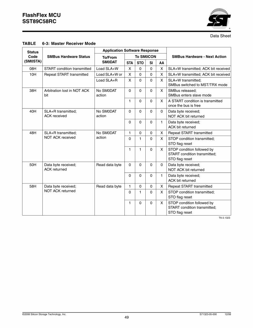
Data Sheet
FlashFlex MCUSST89C58RC
TABLE 6-3: Master Receiver Mode
Status Code
(SM0STA)SMBus Hardware Status
Application Software Response
SMBus Hardware - Next ActionTo/From SM0DAT
To SM0CON
STA STO SI AA
08H START condition transmitted Load SLA+W X 0 0 X SLA+W transmitted; ACK bit received
10H Repeat START transmitted Load SLA+W or X 0 0 X SLA+W transmitted; ACK bit received
Load SLA+R X 0 0 X SLA+W transmitted; SMBus switched to MST/TRX mode
38H Arbitration lost in NOT ACK bit
No SM0DAT action
0 0 0 X SMBus released; SMBus enters slave mode
1 0 0 X A START condition is transmitted once the bus is free
40H SLA+R transmitted; ACK received
No SM0DAT action
0 0 0 0 Data byte received;NOT ACK bit returned
0 0 0 1 Data byte received;ACK bit returned
48H SLA+R transmitted; NOT ACK received
No SM0DAT action
1 0 0 X Repeat START transmitted
0 1 0 X STOP condition transmitted;STO flag reset
1 1 0 X STOP condition followed bySTART condition transmitted;STO flag reset
50H Data byte received;ACK returned
Read data byte 0 0 0 0 Data byte received;NOT ACK bit returned
0 0 0 1 Data byte received;ACK bit returned
58H Data byte received;NOT ACK returned
Read data byte 1 0 0 X Repeat START transmitted
0 1 0 X STOP condition transmitted;STO flag reset
1 0 0 X STOP condition followed bySTART condition transmitted;STO flag reset
T6-3.1323
49©2008 Silicon Storage Technology, Inc. S71323-05-000 12/08
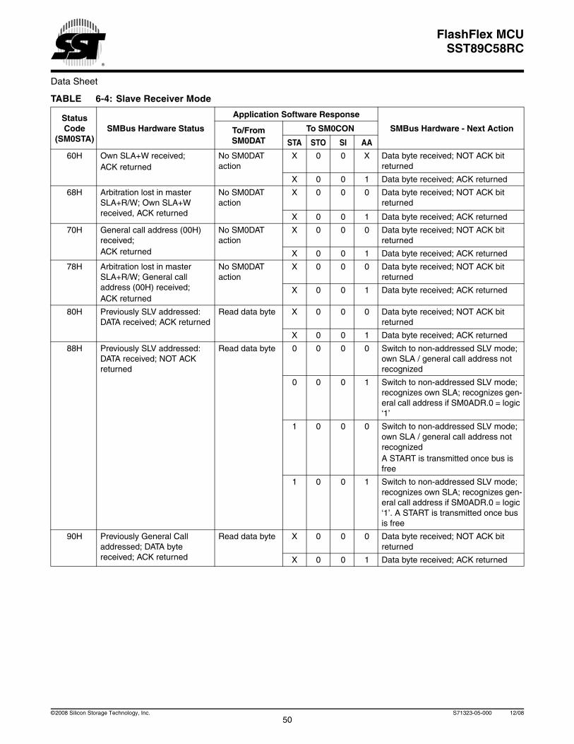
Data Sheet
FlashFlex MCUSST89C58RC
TABLE 6-4: Slave Receiver Mode
Status Code
(SM0STA)SMBus Hardware Status
Application Software Response
SMBus Hardware - Next ActionTo/From SM0DAT
To SM0CON
STA STO SI AA
60H Own SLA+W received;ACK returned
No SM0DAT action
X 0 0 X Data byte received; NOT ACK bit returned
X 0 0 1 Data byte received; ACK returned
68H Arbitration lost in master SLA+R/W; Own SLA+W received, ACK returned
No SM0DAT action
X 0 0 0 Data byte received; NOT ACK bit returned
X 0 0 1 Data byte received; ACK returned
70H General call address (00H) received; ACK returned
No SM0DAT action
X 0 0 0 Data byte received; NOT ACK bit returned
X 0 0 1 Data byte received; ACK returned
78H Arbitration lost in master SLA+R/W; General call address (00H) received; ACK returned
No SM0DAT action
X 0 0 0 Data byte received; NOT ACK bit returned
X 0 0 1 Data byte received; ACK returned
80H Previously SLV addressed: DATA received; ACK returned
Read data byte X 0 0 0 Data byte received; NOT ACK bit returned
X 0 0 1 Data byte received; ACK returned
88H Previously SLV addressed: DATA received; NOT ACK returned
Read data byte 0 0 0 0 Switch to non-addressed SLV mode; own SLA / general call address not recognized
0 0 0 1 Switch to non-addressed SLV mode; recognizes own SLA; recognizes gen-eral call address if SM0ADR.0 = logic ‘1’
1 0 0 0 Switch to non-addressed SLV mode; own SLA / general call address not recognizedA START is transmitted once bus is free
1 0 0 1 Switch to non-addressed SLV mode; recognizes own SLA; recognizes gen-eral call address if SM0ADR.0 = logic ‘1’. A START is transmitted once bus is free
90H Previously General Call addressed; DATA byte received; ACK returned
Read data byte X 0 0 0 Data byte received; NOT ACK bit returned
X 0 0 1 Data byte received; ACK returned
50©2008 Silicon Storage Technology, Inc. S71323-05-000 12/08
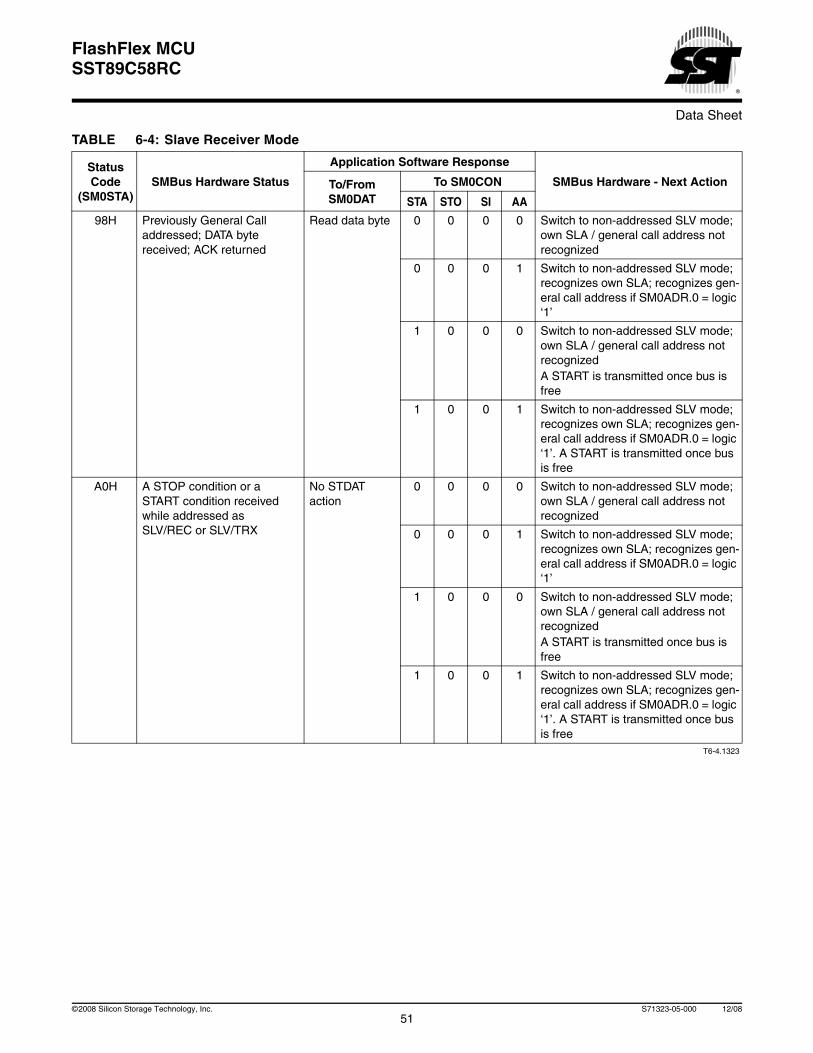
Data Sheet
FlashFlex MCUSST89C58RC
98H Previously General Call addressed; DATA byte received; ACK returned
Read data byte 0 0 0 0 Switch to non-addressed SLV mode; own SLA / general call address not recognized
0 0 0 1 Switch to non-addressed SLV mode; recognizes own SLA; recognizes gen-eral call address if SM0ADR.0 = logic ‘1’
1 0 0 0 Switch to non-addressed SLV mode; own SLA / general call address not recognizedA START is transmitted once bus is free
1 0 0 1 Switch to non-addressed SLV mode; recognizes own SLA; recognizes gen-eral call address if SM0ADR.0 = logic ‘1’. A START is transmitted once bus is free
A0H A STOP condition or a START condition received while addressed as SLV/REC or SLV/TRX
No STDAT action
0 0 0 0 Switch to non-addressed SLV mode; own SLA / general call address not recognized
0 0 0 1 Switch to non-addressed SLV mode; recognizes own SLA; recognizes gen-eral call address if SM0ADR.0 = logic ‘1’
1 0 0 0 Switch to non-addressed SLV mode; own SLA / general call address not recognizedA START is transmitted once bus is free
1 0 0 1 Switch to non-addressed SLV mode; recognizes own SLA; recognizes gen-eral call address if SM0ADR.0 = logic ‘1’. A START is transmitted once bus is free
T6-4.1323
TABLE 6-4: Slave Receiver Mode
Status Code
(SM0STA)SMBus Hardware Status
Application Software Response
SMBus Hardware - Next ActionTo/From SM0DAT
To SM0CON
STA STO SI AA
51©2008 Silicon Storage Technology, Inc. S71323-05-000 12/08
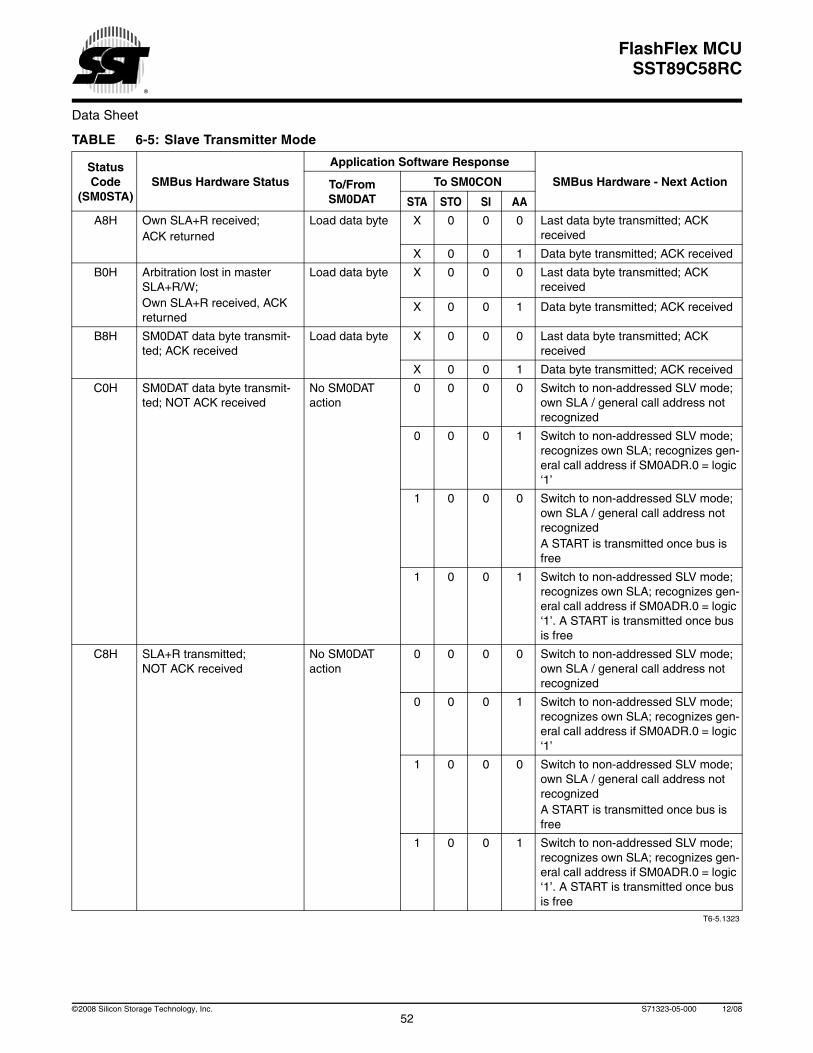
Data Sheet
FlashFlex MCUSST89C58RC
TABLE 6-5: Slave Transmitter Mode
Status Code
(SM0STA)SMBus Hardware Status
Application Software Response
SMBus Hardware - Next ActionTo/From SM0DAT
To SM0CON
STA STO SI AA
A8H Own SLA+R received;ACK returned
Load data byte X 0 0 0 Last data byte transmitted; ACK received
X 0 0 1 Data byte transmitted; ACK received
B0H Arbitration lost in master SLA+R/W;Own SLA+R received, ACK returned
Load data byte X 0 0 0 Last data byte transmitted; ACK received
X 0 0 1 Data byte transmitted; ACK received
B8H SM0DAT data byte transmit-ted; ACK received
Load data byte X 0 0 0 Last data byte transmitted; ACK received
X 0 0 1 Data byte transmitted; ACK received
C0H SM0DAT data byte transmit-ted; NOT ACK received
No SM0DAT action
0 0 0 0 Switch to non-addressed SLV mode; own SLA / general call address not recognized
0 0 0 1 Switch to non-addressed SLV mode; recognizes own SLA; recognizes gen-eral call address if SM0ADR.0 = logic ‘1’
1 0 0 0 Switch to non-addressed SLV mode; own SLA / general call address not recognizedA START is transmitted once bus is free
1 0 0 1 Switch to non-addressed SLV mode; recognizes own SLA; recognizes gen-eral call address if SM0ADR.0 = logic ‘1’. A START is transmitted once bus is free
C8H SLA+R transmitted; NOT ACK received
No SM0DAT action
0 0 0 0 Switch to non-addressed SLV mode; own SLA / general call address not recognized
0 0 0 1 Switch to non-addressed SLV mode; recognizes own SLA; recognizes gen-eral call address if SM0ADR.0 = logic ‘1’
1 0 0 0 Switch to non-addressed SLV mode; own SLA / general call address not recognizedA START is transmitted once bus is free
1 0 0 1 Switch to non-addressed SLV mode; recognizes own SLA; recognizes gen-eral call address if SM0ADR.0 = logic ‘1’. A START is transmitted once bus is free
T6-5.1323
52©2008 Silicon Storage Technology, Inc. S71323-05-000 12/08
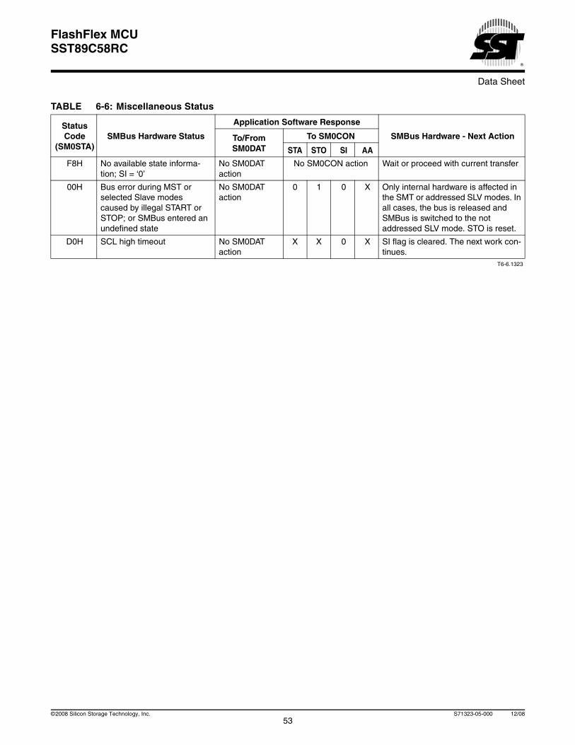
Data Sheet
FlashFlex MCUSST89C58RC
TABLE 6-6: Miscellaneous Status
Status Code
(SM0STA)SMBus Hardware Status
Application Software Response
SMBus Hardware - Next ActionTo/From SM0DAT
To SM0CON
STA STO SI AA
F8H No available state informa-tion; SI = ‘0’
No SM0DAT action
No SM0CON action Wait or proceed with current transfer
00H Bus error during MST or selected Slave modes caused by illegal START or STOP; or SMBus entered an undefined state
No SM0DAT action
0 1 0 X Only internal hardware is affected in the SMT or addressed SLV modes. In all cases, the bus is released and SMBus is switched to the not addressed SLV mode. STO is reset.
D0H SCL high timeout No SM0DAT action
X X 0 X SI flag is cleared. The next work con-tinues.
T6-6.1323
53©2008 Silicon Storage Technology, Inc. S71323-05-000 12/08
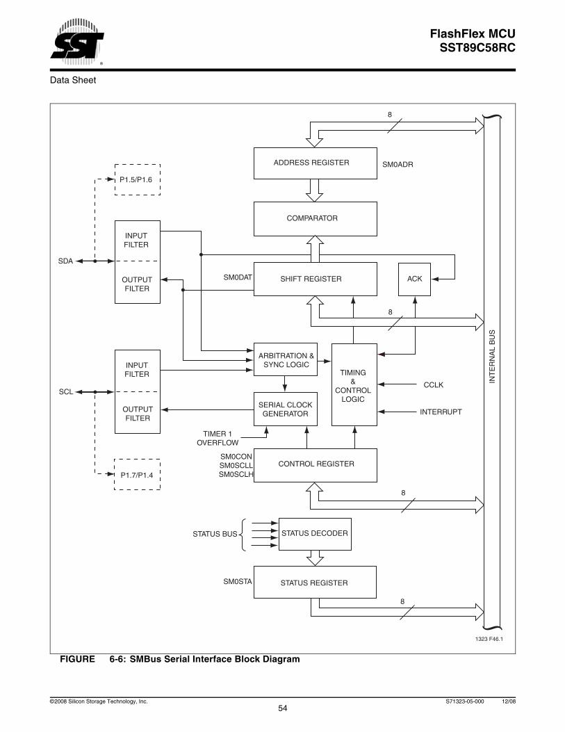
Data Sheet
FlashFlex MCUSST89C58RC
FIGURE 6-6: SMBus Serial Interface Block Diagram
8
ACKSHIFT REGISTER
COMPARATOR
TIMING&
CONTROLLOGIC
INTERRUPT
STATUS REGISTER
STATUS DECODER
CONTROL REGISTER
SERIAL CLOCKGENERATOR
TIMER 1OVERFLOW
STATUS BUS
ARBITRATION &SYNC LOGIC
INPUTFILTER
OUTPUTFILTER
INPUTFILTER
OUTPUTFILTER
P1.5/P1.6
P1.7/P1.4
8
8
INT
ER
NA
L B
US
8
SM0CONSM0SCLLSM0SCLH
SM0STA
CCLK
SM0ADR
SM0DAT
SDA
SCL
1323 F46.1
ADDRESS REGISTER
54©2008 Silicon Storage Technology, Inc. S71323-05-000 12/08
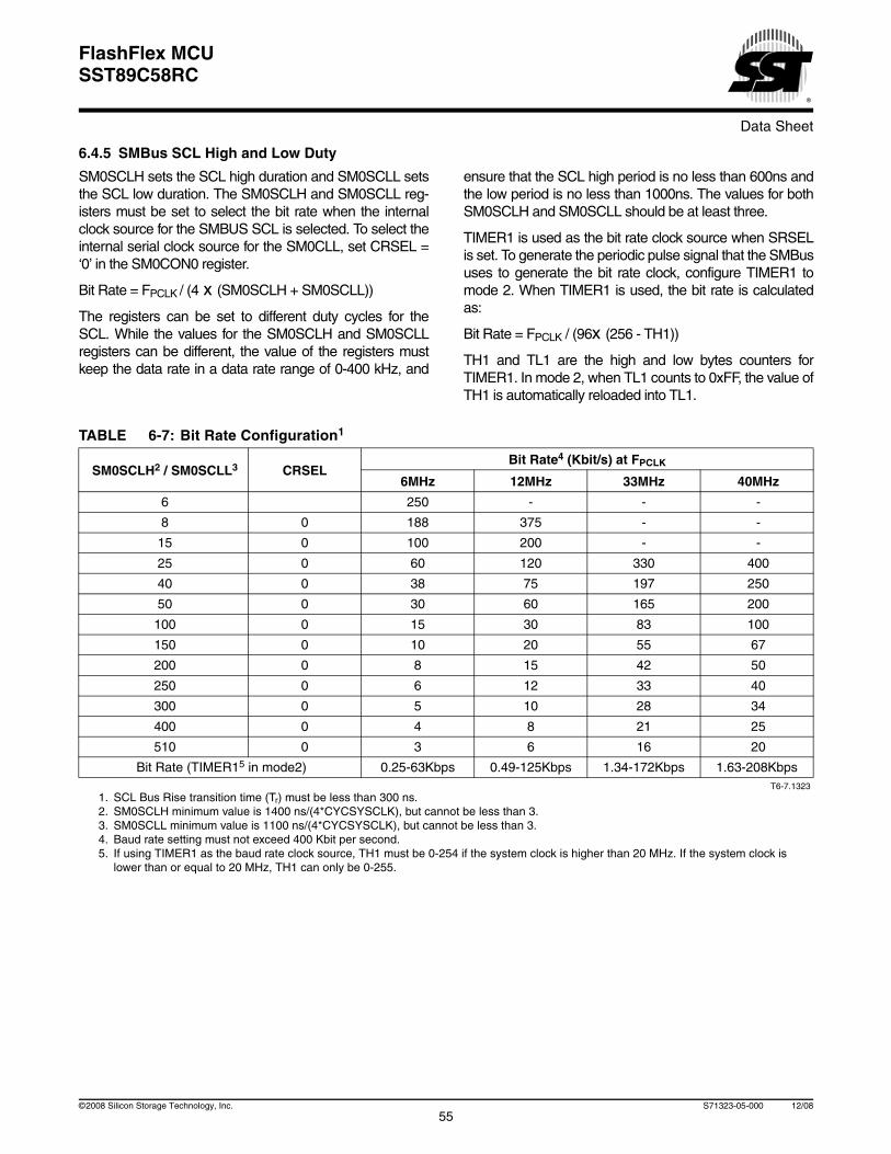
Data Sheet
FlashFlex MCUSST89C58RC
6.4.5 SMBus SCL High and Low Duty
SM0SCLH sets the SCL high duration and SM0SCLL setsthe SCL low duration. The SM0SCLH and SM0SCLL reg-isters must be set to select the bit rate when the internalclock source for the SMBUS SCL is selected. To select theinternal serial clock source for the SM0CLL, set CRSEL =‘0’ in the SM0CON0 register.
Bit Rate = FPCLK / (4 x (SM0SCLH + SM0SCLL))
The registers can be set to different duty cycles for theSCL. While the values for the SM0SCLH and SM0SCLLregisters can be different, the value of the registers mustkeep the data rate in a data rate range of 0-400 kHz, and
ensure that the SCL high period is no less than 600ns andthe low period is no less than 1000ns. The values for bothSM0SCLH and SM0SCLL should be at least three.
TIMER1 is used as the bit rate clock source when SRSELis set. To generate the periodic pulse signal that the SMBususes to generate the bit rate clock, configure TIMER1 tomode 2. When TIMER1 is used, the bit rate is calculatedas:
Bit Rate = FPCLK / (96x (256 - TH1))
TH1 and TL1 are the high and low bytes counters forTIMER1. In mode 2, when TL1 counts to 0xFF, the value ofTH1 is automatically reloaded into TL1.
TABLE 6-7: Bit Rate Configuration1
1. SCL Bus Rise transition time (Tr) must be less than 300 ns.
SM0SCLH2 / SM0SCLL3
2. SM0SCLH minimum value is 1400 ns/(4*CYCSYSCLK), but cannot be less than 3.3. SM0SCLL minimum value is 1100 ns/(4*CYCSYSCLK), but cannot be less than 3.
CRSELBit Rate4 (Kbit/s) at FPCLK
4. Baud rate setting must not exceed 400 Kbit per second.
6MHz 12MHz 33MHz 40MHz
6 250 - - -
8 0 188 375 - -
15 0 100 200 - -
25 0 60 120 330 400
40 0 38 75 197 250
50 0 30 60 165 200
100 0 15 30 83 100
150 0 10 20 55 67
200 0 8 15 42 50
250 0 6 12 33 40
300 0 5 10 28 34
400 0 4 8 21 25
510 0 3 6 16 20
Bit Rate (TIMER15 in mode2)
5. If using TIMER1 as the baud rate clock source, TH1 must be 0-254 if the system clock is higher than 20 MHz. If the system clock is lower than or equal to 20 MHz, TH1 can only be 0-255.
0.25-63Kbps 0.49-125Kbps 1.34-172Kbps 1.63-208Kbps T6-7.1323
55©2008 Silicon Storage Technology, Inc. S71323-05-000 12/08
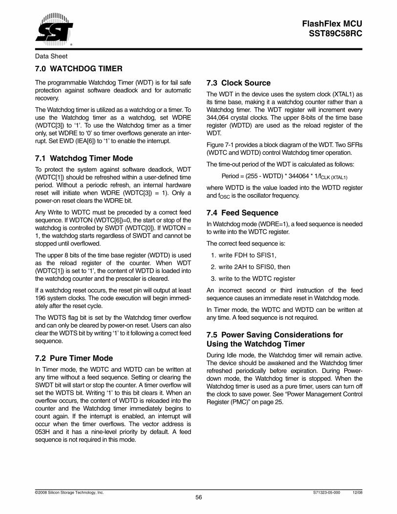
Data Sheet
FlashFlex MCUSST89C58RC
7.0 WATCHDOG TIMER
The programmable Watchdog Timer (WDT) is for fail safeprotection against software deadlock and for automaticrecovery.
The Watchdog timer is utilized as a watchdog or a timer. Touse the Watchdog timer as a watchdog, set WDRE(WDTC[3]) to ‘1’. To use the Watchdog timer as a timeronly, set WDRE to ‘0’ so timer overflows generate an inter-rupt. Set EWD (IEA[6]) to ‘1’ to enable the interrupt.
7.1 Watchdog Timer ModeTo protect the system against software deadlock, WDT(WDTC[1]) should be refreshed within a user-defined timeperiod. Without a periodic refresh, an internal hardwarereset will initiate when WDRE (WDTC[3]) = 1). Only apower-on reset clears the WDRE bit.
Any Write to WDTC must be preceded by a correct feedsequence. If WDTON (WDTC[6])=0, the start or stop of thewatchdog is controlled by SWDT (WDTC[0]). If WDTON =1, the watchdog starts regardless of SWDT and cannot bestopped until overflowed.
The upper 8 bits of the time base register (WDTD) is usedas the reload register of the counter. When WDT(WDTC[1]) is set to ‘1’, the content of WDTD is loaded intothe watchdog counter and the prescaler is cleared.
If a watchdog reset occurs, the reset pin will output at least196 system clocks. The code execution will begin immedi-ately after the reset cycle.
The WDTS flag bit is set by the Watchdog timer overflowand can only be cleared by power-on reset. Users can alsoclear the WDTS bit by writing ‘1’ to it following a correct feedsequence.
7.2 Pure Timer ModeIn Timer mode, the WDTC and WDTD can be written atany time without a feed sequence. Setting or clearing theSWDT bit will start or stop the counter. A timer overflow willset the WDTS bit. Writing ‘1’ to this bit clears it. When anoverflow occurs, the content of WDTD is reloaded into thecounter and the Watchdog timer immediately begins tocount again. If the interrupt is enabled, an interrupt willoccur when the timer overflows. The vector address is053H and it has a nine-level priority by default. A feedsequence is not required in this mode.
7.3 Clock SourceThe WDT in the device uses the system clock (XTAL1) asits time base, making it a watchdog counter rather than aWatchdog timer. The WDT register will increment every344,064 crystal clocks. The upper 8-bits of the time baseregister (WDTD) are used as the reload register of theWDT.
Figure 7-1 provides a block diagram of the WDT. Two SFRs(WDTC and WDTD) control Watchdog timer operation.
The time-out period of the WDT is calculated as follows:
Period = (255 - WDTD) * 344064 * 1/fCLK (XTAL1)
where WDTD is the value loaded into the WDTD registerand fOSC is the oscillator frequency.
7.4 Feed SequenceIn Watchdog mode (WDRE=1), a feed sequence is neededto write into the WDTC register.
The correct feed sequence is:
1. write FDH to SFIS1,
2. write 2AH to SFIS0, then
3. write to the WDTC register
An incorrect second or third instruction of the feedsequence causes an immediate reset in Watchdog mode.
In Timer mode, the WDTC and WDTD can be written atany time. A feed sequence is not required.
7.5 Power Saving Considerations for Using the Watchdog TimerDuring Idle mode, the Watchdog timer will remain active.The device should be awakened and the Watchdog timerrefreshed periodically before expiration. During Power-down mode, the Watchdog timer is stopped. When theWatchdog timer is used as a pure timer, users can turn offthe clock to save power. See “Power Management ControlRegister (PMC)” on page 25.
56©2008 Silicon Storage Technology, Inc. S71323-05-000 12/08
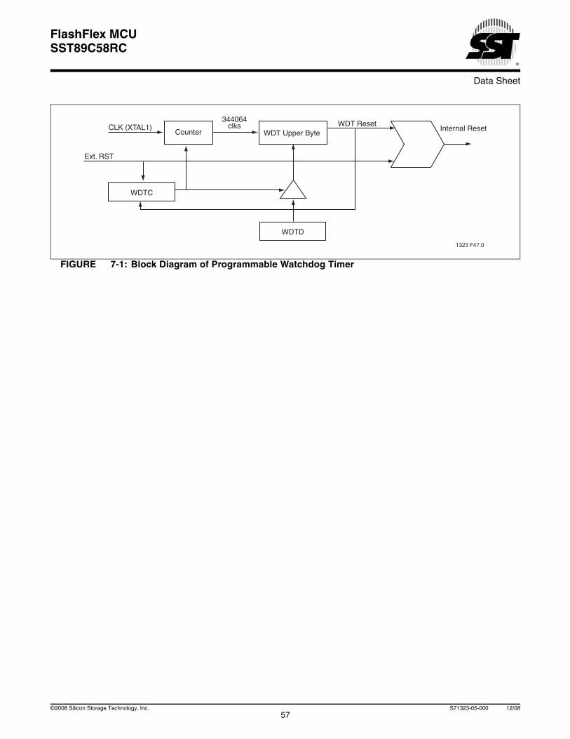
Data Sheet
FlashFlex MCUSST89C58RC
FIGURE 7-1: Block Diagram of Programmable Watchdog Timer
1323 F47.0
WDT Upper ByteWDT Reset
Internal Reset344064
clksCounter
CLK (XTAL1)
Ext. RST
WDTC
WDTD
57©2008 Silicon Storage Technology, Inc. S71323-05-000 12/08

Data Sheet
FlashFlex MCUSST89C58RC
8.0 SECURITY LOCK
The security lock protects against software piracy and pre-vents the contents of the flash from being read by unautho-rized parties. It also protects against code corruptionresulting from accidental erasing and programming to theinternal flash memory. There are two different types ofsecurity locks in the device security lock system: Chip-Level Security Lock and Page-Level Security Lock.
8.1 Chip-Level Security LockThere are four types of chip-level security locks.
1. Disable External MOVC instruction
2. Disable External Host Mode (Except Read Chip ID and Chip-Erase commands)
3. Disable Boot from External Memory
4. Disable External IAP commands (Except Chip-Erase commands)
Users can turn on these security locks in any combinationto achieve the security protection scheme. To unlock secu-rity locks, the Chip-Erase command must be used.
8.1.1 Disable External MOVC instruction
When Disable-Extern-MOVC command is executed eitherby External Host Mode command or IAP Mode Command,MOVC instructions executed from external program mem-ory are disabled from fetching code bytes from internalmemory.
8.1.2 Disable External Host Mode
When Disable-Extern-Host-Cmd command is executedeither by External Host Mode Command or IAP ModeCommand, all external host mode commands are disabledexcept Chip-Erase command and Read-ID command.
Upon activation of this option, the device can not beaccessed through external host mode. User can not verifyand copy the contents of the internal flash
8.1.3 Disable Boot From External Memory
When Disable-Extern-Boot command is executed either byExternal Host Mode Command or IAP Mode Command,the EA pin value will be ignored during chip Reset andalways boot from the internal memory.
8.1.4 Disable External IAP Commands
When Disable-Extern-IAP command is executed either byExternal Host Mode Command or IAP Mode Command, allIAP commands executed from external memory are dis-abled except Chip-Erase command. All IAP commandsexecuted from internal memory are allowed if the PageLock is not set.
8.2 Page-Level Security LockWhen any of Secure-Page0, Secure-Page1, Secure-Page2, Secure-Page3, or Secure-Page4 command is exe-cuted, the individual page (Page0, Page1, Page2, Page3,or Page4) will enter secured mode. No part of the page canbe verified by either External Host mode commands or IAPcommands. MOVC instructions are also unable to read anydata from the page.
To unlock the security locks on Page0-3 of the primary par-tition (Partition0), the Partition0-Erase command must beused. To unlock the security lock on Page4, the Chip-Erasecommand must be used.
8.3 Read Operation Under Lock ConditionThe following three cases can be used to indicate the Readoperation is targeting a locked, secured memory area:
1. External host mode: Read-back = 55H (locked)
2. IAP command: Read-back = previous SFDT data
3. MOVC: Read-back = 00H (blank)
58©2008 Silicon Storage Technology, Inc. S71323-05-000 12/08
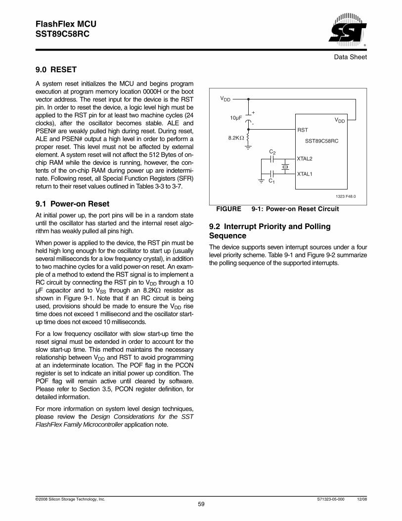
Data Sheet
FlashFlex MCUSST89C58RC
9.0 RESET
A system reset initializes the MCU and begins programexecution at program memory location 0000H or the bootvector address. The reset input for the device is the RSTpin. In order to reset the device, a logic level high must beapplied to the RST pin for at least two machine cycles (24clocks), after the oscillator becomes stable. ALE andPSEN# are weakly pulled high during reset. During reset,ALE and PSEN# output a high level in order to perform aproper reset. This level must not be affected by externalelement. A system reset will not affect the 512 Bytes of on-chip RAM while the device is running, however, the con-tents of the on-chip RAM during power up are indetermi-nate. Following reset, all Special Function Registers (SFR)return to their reset values outlined in Tables 3-3 to 3-7.
9.1 Power-on ResetAt initial power up, the port pins will be in a random stateuntil the oscillator has started and the internal reset algo-rithm has weakly pulled all pins high.
When power is applied to the device, the RST pin must beheld high long enough for the oscillator to start up (usuallyseveral milliseconds for a low frequency crystal), in additionto two machine cycles for a valid power-on reset. An exam-ple of a method to extend the RST signal is to implement aRC circuit by connecting the RST pin to VDD through a 10µF capacitor and to VSS through an 8.2KΩ resistor asshown in Figure 9-1. Note that if an RC circuit is beingused, provisions should be made to ensure the VDD risetime does not exceed 1 millisecond and the oscillator start-up time does not exceed 10 milliseconds.
For a low frequency oscillator with slow start-up time thereset signal must be extended in order to account for theslow start-up time. This method maintains the necessaryrelationship between VDD and RST to avoid programmingat an indeterminate location. The POF flag in the PCONregister is set to indicate an initial power up condition. ThePOF flag will remain active until cleared by software.Please refer to Section 3.5, PCON register definition, fordetailed information.
For more information on system level design techniques,please review the Design Considerations for the SSTFlashFlex Family Microcontroller application note.
FIGURE 9-1: Power-on Reset Circuit
9.2 Interrupt Priority and Polling SequenceThe device supports seven interrupt sources under a fourlevel priority scheme. Table 9-1 and Figure 9-2 summarizethe polling sequence of the supported interrupts.
1323 F48.0
VDD
VDD
10µF+
-
8.2KSST89C58RC
RST
XTAL2
XTAL1C1
C2
59©2008 Silicon Storage Technology, Inc. S71323-05-000 12/08
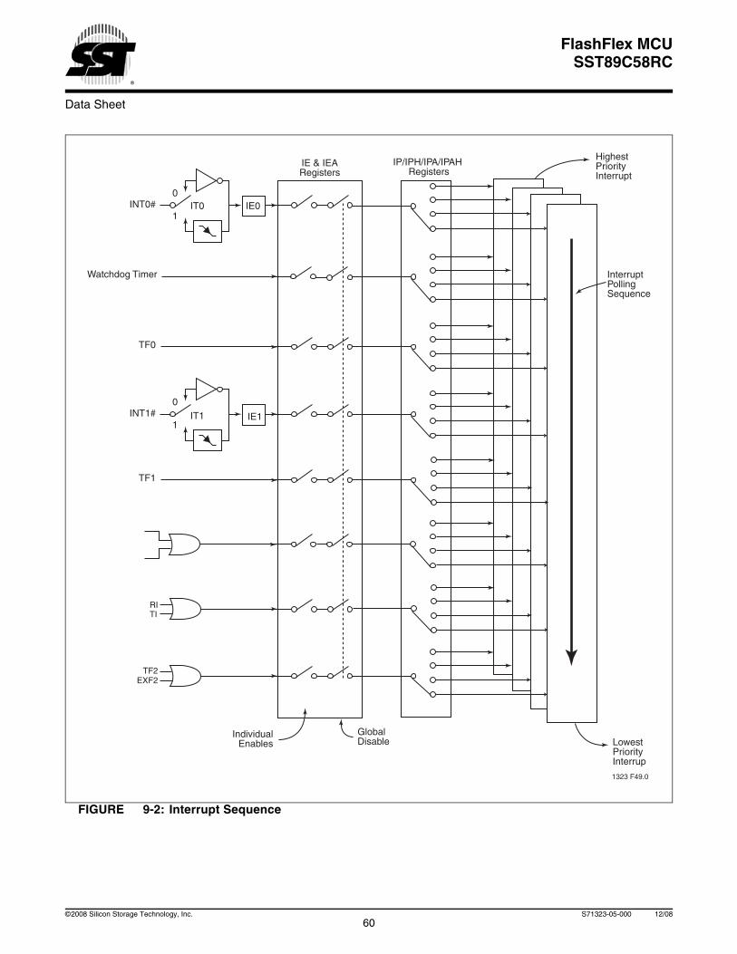
Data Sheet
FlashFlex MCUSST89C58RC
FIGURE 9-2: Interrupt Sequence
IE1INT1#
IndividualEnables
TF1
TF0
RI
0
1
IE0
GlobalDisable
HighestPriorityInterrupt
InterruptPollingSequence
LowestPriorityInterrup
IT0
IT1
INT0#
IE & IEARegisters
IP/IPH/IPA/IPAH Registers
0
1
TF2EXF2
TI
Watchdog Timer
1323 F49.0
60©2008 Silicon Storage Technology, Inc. S71323-05-000 12/08
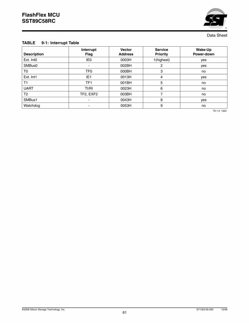
Data Sheet
FlashFlex MCUSST89C58RC
TABLE 9-1: Interrupt Table
DescriptionInterrupt
FlagVector
AddressServicePriority
Wake-UpPower-down
Ext. Int0 IE0 0003H 1(highest) yes
SMBus0 - 002BH 2 yes
T0 TF0 000BH 3 no
Ext. Int1 IE1 0013H 4 yes
T1 TF1 001BH 5 no
UART TI/RI 0023H 6 no
T2 TF2, EXF2 003BH 7 no
SMBus1 - 0043H 8 yes
Watchdog - 0053H 9 noT9-1.0 1323
61©2008 Silicon Storage Technology, Inc. S71323-05-000 12/08
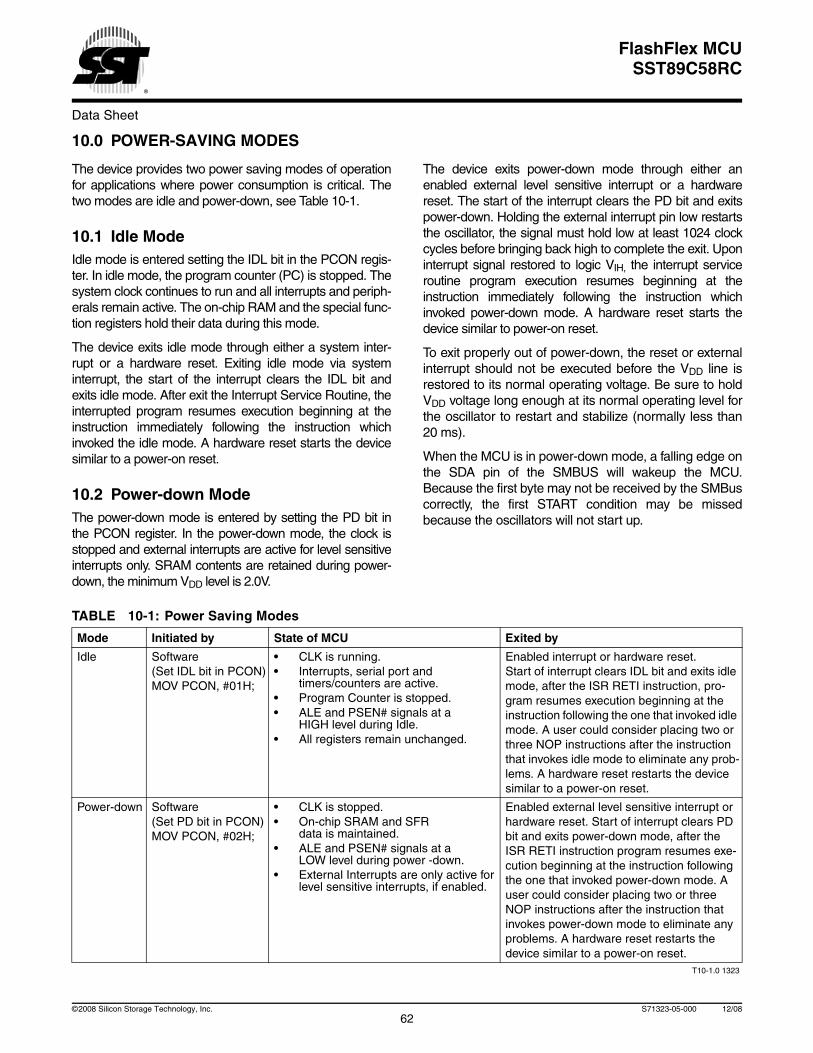
Data Sheet
FlashFlex MCUSST89C58RC
10.0 POWER-SAVING MODES
The device provides two power saving modes of operationfor applications where power consumption is critical. Thetwo modes are idle and power-down, see Table 10-1.
10.1 Idle ModeIdle mode is entered setting the IDL bit in the PCON regis-ter. In idle mode, the program counter (PC) is stopped. Thesystem clock continues to run and all interrupts and periph-erals remain active. The on-chip RAM and the special func-tion registers hold their data during this mode.
The device exits idle mode through either a system inter-rupt or a hardware reset. Exiting idle mode via systeminterrupt, the start of the interrupt clears the IDL bit andexits idle mode. After exit the Interrupt Service Routine, theinterrupted program resumes execution beginning at theinstruction immediately following the instruction whichinvoked the idle mode. A hardware reset starts the devicesimilar to a power-on reset.
10.2 Power-down ModeThe power-down mode is entered by setting the PD bit inthe PCON register. In the power-down mode, the clock isstopped and external interrupts are active for level sensitiveinterrupts only. SRAM contents are retained during power-down, the minimum VDD level is 2.0V.
The device exits power-down mode through either anenabled external level sensitive interrupt or a hardwarereset. The start of the interrupt clears the PD bit and exitspower-down. Holding the external interrupt pin low restartsthe oscillator, the signal must hold low at least 1024 clockcycles before bringing back high to complete the exit. Uponinterrupt signal restored to logic VIH, the interrupt serviceroutine program execution resumes beginning at theinstruction immediately following the instruction whichinvoked power-down mode. A hardware reset starts thedevice similar to power-on reset.
To exit properly out of power-down, the reset or externalinterrupt should not be executed before the VDD line isrestored to its normal operating voltage. Be sure to holdVDD voltage long enough at its normal operating level forthe oscillator to restart and stabilize (normally less than20 ms).
When the MCU is in power-down mode, a falling edge onthe SDA pin of the SMBUS will wakeup the MCU.Because the first byte may not be received by the SMBuscorrectly, the first START condition may be missedbecause the oscillators will not start up.
TABLE 10-1: Power Saving Modes
Mode Initiated by State of MCU Exited by
Idle Software(Set IDL bit in PCON)MOV PCON, #01H;
• CLK is running. • Interrupts, serial port and
timers/counters are active.• Program Counter is stopped.• ALE and PSEN# signals at a
HIGH level during Idle.• All registers remain unchanged.
Enabled interrupt or hardware reset. Start of interrupt clears IDL bit and exits idle mode, after the ISR RETI instruction, pro-gram resumes execution beginning at the instruction following the one that invoked idle mode. A user could consider placing two or three NOP instructions after the instruction that invokes idle mode to eliminate any prob-lems. A hardware reset restarts the device similar to a power-on reset.
Power-down Software(Set PD bit in PCON)MOV PCON, #02H;
• CLK is stopped.• On-chip SRAM and SFR
data is maintained.• ALE and PSEN# signals at a
LOW level during power -down.• External Interrupts are only active for
level sensitive interrupts, if enabled.
Enabled external level sensitive interrupt or hardware reset. Start of interrupt clears PD bit and exits power-down mode, after the ISR RETI instruction program resumes exe-cution beginning at the instruction following the one that invoked power-down mode. A user could consider placing two or three NOP instructions after the instruction that invokes power-down mode to eliminate any problems. A hardware reset restarts the device similar to a power-on reset.
T10-1.0 1323
62©2008 Silicon Storage Technology, Inc. S71323-05-000 12/08
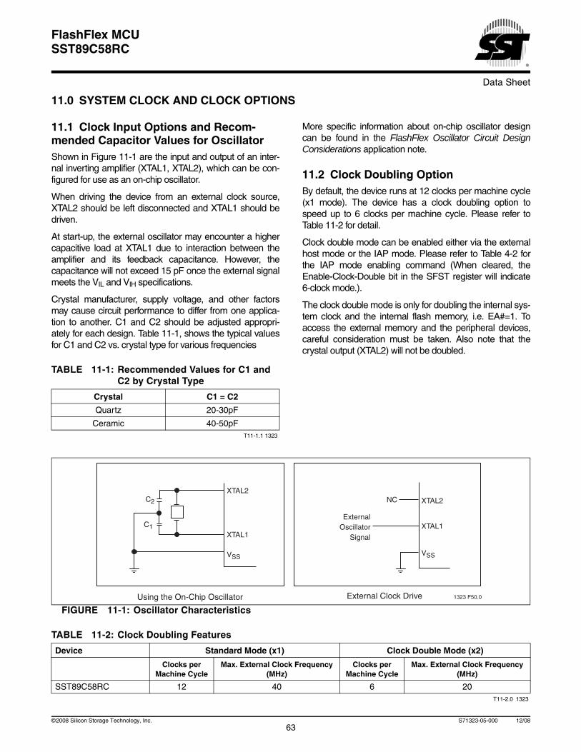
Data Sheet
FlashFlex MCUSST89C58RC
11.0 SYSTEM CLOCK AND CLOCK OPTIONS
11.1 Clock Input Options and Recom-mended Capacitor Values for OscillatorShown in Figure 11-1 are the input and output of an inter-nal inverting amplifier (XTAL1, XTAL2), which can be con-figured for use as an on-chip oscillator.
When driving the device from an external clock source,XTAL2 should be left disconnected and XTAL1 should bedriven.
At start-up, the external oscillator may encounter a highercapacitive load at XTAL1 due to interaction between theamplifier and its feedback capacitance. However, thecapacitance will not exceed 15 pF once the external signalmeets the VIL and VIH specifications.
Crystal manufacturer, supply voltage, and other factorsmay cause circuit performance to differ from one applica-tion to another. C1 and C2 should be adjusted appropri-ately for each design. Table 11-1, shows the typical valuesfor C1 and C2 vs. crystal type for various frequencies
More specific information about on-chip oscillator designcan be found in the FlashFlex Oscillator Circuit DesignConsiderations application note.
11.2 Clock Doubling OptionBy default, the device runs at 12 clocks per machine cycle(x1 mode). The device has a clock doubling option tospeed up to 6 clocks per machine cycle. Please refer toTable 11-2 for detail.
Clock double mode can be enabled either via the externalhost mode or the IAP mode. Please refer to Table 4-2 forthe IAP mode enabling command (When cleared, theEnable-Clock-Double bit in the SFST register will indicate6-clock mode.).
The clock double mode is only for doubling the internal sys-tem clock and the internal flash memory, i.e. EA#=1. Toaccess the external memory and the peripheral devices,careful consideration must be taken. Also note that thecrystal output (XTAL2) will not be doubled.
FIGURE 11-1: Oscillator Characteristics
TABLE 11-1: Recommended Values for C1 and C2 by Crystal Type
Crystal C1 = C2
Quartz 20-30pF
Ceramic 40-50pFT11-1.1 1323
TABLE 11-2: Clock Doubling Features
Device Standard Mode (x1) Clock Double Mode (x2)
Clocks perMachine Cycle
Max. External Clock Frequency(MHz)
Clocks perMachine Cycle
Max. External Clock Frequency(MHz)
SST89C58RC 12 40 6 20T11-2.0 1323
1323 F50.0
XTAL2
XTAL1
VSS
C1
Using the On-Chip Oscillator External Clock Drive
C2 XTAL2
XTAL1
VSS
ExternalOscillator
Signal
NC
63©2008 Silicon Storage Technology, Inc. S71323-05-000 12/08
Data Sheet
FlashFlex MCUSST89C58RC
12.0 ELECTRICAL SPECIFICATION
Note: This specification contains preliminary information on new products in production.The specifications are subject to change without notice.
Absolute Maximum Stress Ratings (Applied conditions greater than those listed under “Absolute MaximumStress Ratings” may cause permanent damage to the device. This is a stress rating only and functional operationof the device at these conditions or conditions greater than those defined in the operational sections of this datasheet is not implied. Exposure to absolute maximum stress rating conditions may affect device reliability.)
Ambient Temperature Under Bias . . . . . . . . . . . . . . . . . . . . . . . . . . . . . . . . . . . . . . . . . . . . . . . . . . -55°C to +125°CStorage Temperature . . . . . . . . . . . . . . . . . . . . . . . . . . . . . . . . . . . . . . . . . . . . . . . . . . . . . . . . . . . . -65°C to +150°CVoltage on EA# Pin to VSS . . . . . . . . . . . . . . . . . . . . . . . . . . . . . . . . . . . . . . . . . . . . . . . . . . . . . . . . . -0.5V to +14.0VD.C. Voltage on Any Pin to Ground Potential . . . . . . . . . . . . . . . . . . . . . . . . . . . . . . . . . . . . . . . . . -0.5V to VDD+0.5VTransient Voltage (<20ns) on Any Other Pin to VSS . . . . . . . . . . . . . . . . . . . . . . . . . . . . . . . . . . . . -1.0V to VDD+1.0VMaximum IOL per I/O Pins P1.4, P1.5, P1.6, P1.7 . . . . . . . . . . . . . . . . . . . . . . . . . . . . . . . . . . . . . . . . . . . . . . .20mAMaximum IOL per I/O for All Other Pins . . . . . . . . . . . . . . . . . . . . . . . . . . . . . . . . . . . . . . . . . . . . . . . . . . . . . . .15mAPackage Power Dissipation Capability (TA = 25°C) . . . . . . . . . . . . . . . . . . . . . . . . . . . . . . . . . . . . . . . . . . . . . . 1.5WThrough Hole Lead Soldering Temperature (10 Seconds). . . . . . . . . . . . . . . . . . . . . . . . . . . . . . . . . . . . . . . . 300°CSurface Mount Solder Reflow Temperature1 . . . . . . . . . . . . . . . . . . . . . . . . . . . . . . . . . . . . . . 260°C for 10 seconds
1. Excluding certain with-Pb 32-PLCC units, all packages are 260°C capable in both non-Pb and with-Pb solder versions.Certain with-Pb 32-PLCC package types are capable of 240°C for 10 seconds; please consult the factory for the latest information.
Output Short Circuit Current2 . . . . . . . . . . . . . . . . . . . . . . . . . . . . . . . . . . . . . . . . . . . . . . . . . . . . . . . . . . . . . 50 mA
2. Outputs shorted for no more than one second. No more than one output shorted at a time.(Based on package heat transfer limitations, not device power consumption.
TABLE 12-1: Operating Range
Symbol Description Min. Max Unit
TA
Ambient Temperature Under Bias
Standard 0 +70 °C
Industrial -40 +85 °C
VDD Supply Voltage
SST89C58RC 2.7 5.5 V
FOSC Oscillator Frequency
SST89C58RC 0 40 MHz
Oscillator Frequency for In-Application programming
SST89C58RC 25 40 MHzT12-1.1 1323
TABLE 12-2: Reliability Characteristics
Symbol Parameter Minimum Specification Units Test Method
NEND1
1. This parameter is measured only for initial qualification and after a design or process change that could affect this parameter.
Endurance 10,000 Cycles JEDEC Standard A117
TDR1 Data Retention 100 Years JEDEC Standard A103
ILTH1 Latch Up 100 + IDD mA JEDEC Standard 78
T12-2.0 1323
64©2008 Silicon Storage Technology, Inc. S71323-05-000 12/08
Data Sheet
FlashFlex MCUSST89C58RC
TABLE 12-3: AC Conditions of Test
Input Rise/Fall Time . . . . . . . . . . . . . . . 10 ns
Output Load . . . . . . . . . . . . . . . . . . . . . CL = 100 pF
See Figures 12-5 and 12-7T12-3.0 1323
TABLE 12-4: Recommended System Power-up Timings
Symbol Parameter Minimum Units
TPU-READ1
1. This parameter is measured only for initial qualification and after a design or process change that could affect this parameter
Power-up to Read Operation 100 µs
TPU-WRITE1 Power-up to Write Operation 100 µs
T12-4.2 1323
TABLE 12-5: Pin Impedance (VDD=3.3V, TA=25 °C, f=1 Mhz, other pins open)
Parameter Description Test Condition Maximum
CI/O1
1. This parameter is measured only for initial qualification and after a design or process change that could affect this parameter.
I/O Pin Capacitance VI/O = 0V 15 pF
CIN1 Input Capacitance VIN = 0V 12 pF
LPIN2
2. Refer to PCI spec.
Pin Inductance 20 nHT12-5.4 1323
65©2008 Silicon Storage Technology, Inc. S71323-05-000 12/08
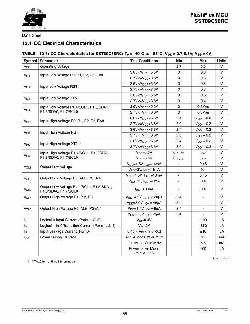
Data Sheet
FlashFlex MCUSST89C58RC
12.1 DC Electrical Characteristics
TABLE 12-6: DC Characteristics for SST89C58RC: TA = -40°C to +85°C; VDD = 2.7-5.5V; VSS = 0V
Symbol Parameter Test Conditions Min Max Units
VDD Operating Voltage 2.7 5.5 V
VIL1 Input Low Voltage P0, P1, P2, P3, EA#3.6V<VDD<=5.5V 0 0.8 V
2.7V<=VDD=3.6V 0 0.6 V
VIL2 Input Low Voltage RST3.6V<VDD<=5.5V 0 0.8 V
2.7V<=VDD=3.6V 0 0.6 V
VIL3 Input Low Voltage XTAL3.6V<VDD<=5.5V 0 0.8 V
2.7V<=VDD=3.6V 0 0.4 V
VIL4Input Low Voltage P1.4/SCL1, P1.5/SDA1, P1.6/SDA0, P1.7/SCL0
3.6V<VDD<=5.5V 0 0.3VDD V
2.7V<=VDD=3.6V 0 0.3VDD V
VIH1 Input High Voltage P0, P1, P2, P3, EA#3.6V<VDD<=5.5V 2.4 VDD + 0.2 V
2.7V<=VDD=3.6V 2.0 VDD + 0.2 V
VIH2 Input High Voltage RST3.6V<VDD<=5.5V 2.4 VDD + 0.2 V
2.7V<=VDD=3.6V 2.0 VDD + 0.2 V
VIH3 Input High Voltage XTAL1
1. XTAL2 is not 5-volt tolerant pin
3.6V<VDD<=5.5V 2.4 VDD + 0.2 V
2.7V<=VDD=3.6V 2.0 VDD + 0.2 V
VIH4Input High Voltage P1.4/SCL1, P1.5/SDA1, P1.6/SDA0, P1.7/SCL0
VDD=5.5V 0.7VDD 5.5 V
VDD=3.0V 0.7VDD 5.5 V
VOL1 Output Low VoltageVDD=4.5V, IOL=+4mA - 0.45 V
VDD=3V, IOL=+4mA - 0.4 V
VOL2 Output Low Voltage P0, ALE, PSEN#VDD=4.5V, IOL=+10mA - 0.45 V
VDD=3V, IOL=+6mA - 0.4 V
VOL3Output Low Voltage P1.4/SCL1, P1.5/SDA1, P1.6/SDA0, P1.7/SCL0
IOL=3.0 mA - 0.4 V
VOH1 Output High Voltage P1, P 2, P3 VDD=4.5V, IOH=-120µA 2.4 - V
VDD=3.0V, IOH=-45µA 2.4 - V
VOH2 Output High Voltage P0, ALE, PSEN# VDD=4.5V, IOH=-8µA 2.4 - V
VDD=3.0V, IOH=-3µA 2.4 - V
IIL Logical 0 Input Current (Ports 1, 2, 3) VIN=0.4V -100 µA
ITL Logical 1-to-0 Transition Current (Ports 1, 2, 3) VIN=2V -650 µA
ILI Input Leakage Current (Port 0) 0.45 < VIN < VDD-0.3 ±10 µA
IDD Power Supply Current Active Mode @ 40MHz 15 mA
Idle Mode @ 40MHz 6.8 mA
Power-down Mode (min V= 5V)
100 µA
T12-6.0 1323
66©2008 Silicon Storage Technology, Inc. S71323-05-000 12/08

Data Sheet
FlashFlex MCUSST89C58RC
12.2 AC Electrical Characteristics
AC Characteristics: (Over Operating Conditions: Load Capacitance for Port 0, ALE, and PSEN# = 100pF;Load Capacitance for All Other Outputs = 80pF)
TABLE 12-7: AC Electrical Characteristics TA = -40°C to +85°C, 2.7-5.5V@40MHz, VSS = 0V
Symbol Parameter
Oscillator
Units
40 MHz (x1 Mode)20 MHz (x2 Mode)1
1. Calculated values are for x1 Mode only
Variable
Min Max Min Max
1/TCLCL x1 Mode Oscillator Frequency 0 40 0 40 MHz
1/2TCLCL x2 Mode Oscillator Frequency 0 20 0 20 MHz
TLHLL ALE Pulse Width 35 2TCLCL - 15 ns
TAVLL Address Valid to ALE Low 10 TCLCL - 15 (5V) ns
TLLAX Address Hold After ALE Low 10 TCLCL - 15 (5V) ns
TLLIV ALE Low to Valid Instr In 55 4TCLCL - 45 (5V) ns
TLLPL ALE Low to PSEN# Low 10 TCLCL - 15 (5V) ns
TPLPH PSEN# Pulse Width 60 3TCLCL - 15 (5V) ns
TPLIV PSEN# Low to Valid Instr In 25 3TCLCL - 50 (5V) ns
TPXIX Input Instr Hold After PSEN# 0 ns
TPXIZ Input Instr Float After PSEN# 10 TCLCL - 15 (5V) ns
TPXAV PSEN# to Address valid 17 TCLCL - 8 ns
TAVIV Address to Valid Instr In 65 5TCLCL - 60 (5V) ns
TPLAZ PSEN# Low to Address Float 10 10 ns
TRLRH RD# Pulse Width 120 6TCLCL - 30 (5V) ns
TWLWH Write Pulse Width (WE#) 120 6TCLCL - 30 (5V) ns
TRLDV RD# Low to Valid Data In 75 5TCLCL - 50 (5V) ns
TRHDX Data Hold After RD# 0 0 ns
TRHDZ Data Float After RD# 38 2TCLCL - 12 (5V) ns
TLLDV ALE Low to Valid Data In 150 8TCLCL - 50 (5V) ns
TAVDV Address to Valid Data In 150 9TCLCL - 75 (5V) ns
TLLWL ALE Low to RD# or WR# Low 60 90 3TCLCL - 15 (5V) 3TCLCL + 15 (5V) ns
TAVWL Address to RD# or WR# Low 70 4TCLCL - 30 (5V) ns
TQVWX Data Valid to WR# High to Low Transition 5 TCLCL - 20 ns
TWHQX Data Hold After WR# 5 TCLCL - 20 (5V) ns
TQVWH Data Valid to WR# High 125 7TCLCL - 50 (5V) ns
TRLAZ RD# Low to Address Float 0 0 ns
TWHLH RD# to WR# High to ALE High 10 40 TCLCL - 15 (5V) TCLCL + 15 (5V) ns
TOFSB SMBUS Output fall time from VIH min to VIL max with a bus capacitance100pf
30 (5V) 250 (5V) ns
T12-7.0 1323
67©2008 Silicon Storage Technology, Inc. S71323-05-000 12/08
Data Sheet
FlashFlex MCUSST89C58RC
Explanation of Symbols Each timing symbol has 5 characters. The first character is always a ‘T’ (stands fortime). The other characters, depending on their positions, stand for the name of a signal or the logical status of thatsignal. The following is a list of all the characters and what they stand for.
For example:
TAVLL = Time from Address Valid to ALE Low
TLLPL = Time from ALE Low to PSEN# Low
A: Address Q: Output dataC: Clock R: RD# signalD: Input data T: TimeH: Logic level HIGH V: ValidI: Instruction (program memory contents) W: WR# signalL: Logic level LOW or ALE X: No longer a valid logic levelP: PSEN# Z: High Impedance (Float)
68©2008 Silicon Storage Technology, Inc. S71323-05-000 12/08
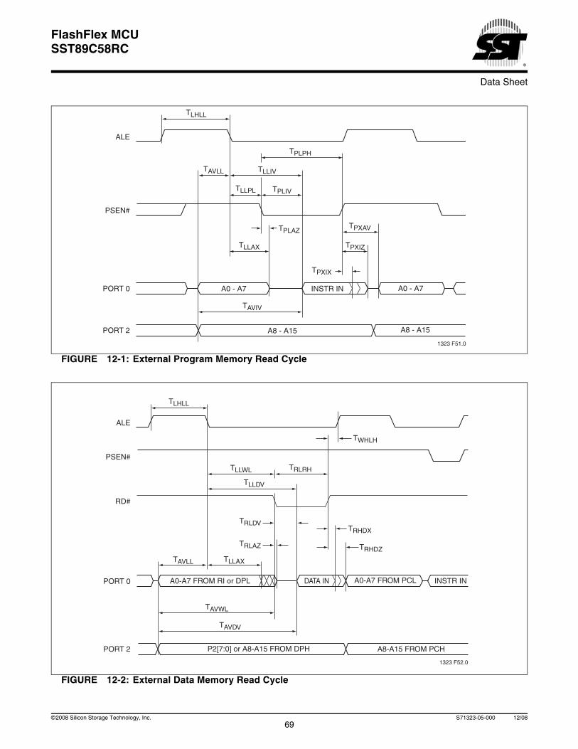
Data Sheet
FlashFlex MCUSST89C58RC
FIGURE 12-1: External Program Memory Read Cycle
FIGURE 12-2: External Data Memory Read Cycle
1323 F51.0
PORT 2
PORT 0
PSEN#
ALE
A0 - A7
TLLAX
TPLAZ
TPXIZ
TLLPL
TAVIV
TAVLL
TPXIX
TLHLL
TLLIV
TPLIV
TPLPH
INSTR IN
A8 - A15 A8 - A15
A0 - A7
TPXAV
1323 F52.0
PORT 2
PORT 0
RD#
PSEN#
ALE
TLHLL
P2[7:0] or A8-A15 FROM DPH
A0-A7 FROM RI or DPL
TAVDV
TAVWL
DATA IN INSTR IN
TRLAZ
TAVLL TLLAX
TLLWL
TLLDV
TRLRH
TRLDV
TRHDZ
TWHLH
TRHDX
A8-A15 FROM PCH
A0-A7 FROM PCL
69©2008 Silicon Storage Technology, Inc. S71323-05-000 12/08
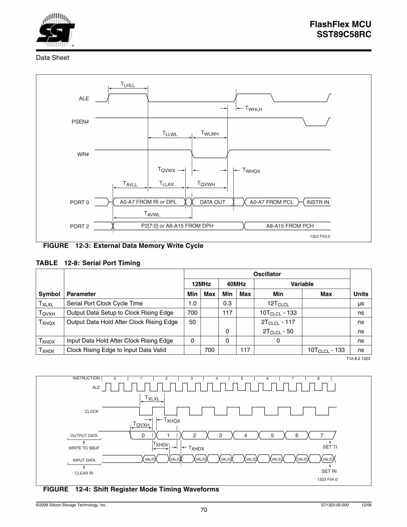
Data Sheet
FlashFlex MCUSST89C58RC
FIGURE 12-3: External Data Memory Write Cycle
FIGURE 12-4: Shift Register Mode Timing Waveforms
TABLE 12-8: Serial Port Timing
Symbol Parameter
Oscillator
Units
12MHz 40MHz Variable
Min Max Min Max Min Max
TXLXL Serial Port Clock Cycle Time 1.0 0.3 12TCLCL µs
TQVXH Output Data Setup to Clock Rising Edge 700 117 10TCLCL - 133 ns
TXHQX Output Data Hold After Clock Rising Edge 50 2TCLCL - 117 ns
0 2TCLCL - 50 ns
TXHDX Input Data Hold After Clock Rising Edge 0 0 0 ns
TXHDV Clock Rising Edge to Input Data Valid 700 117 10TCLCL - 133 nsT12-8.2 1323
1323 F53.0
PORT 2
PORT 0
WR#
PSEN#
ALE
TLHLL
P2[7:0] or A8-A15 FROM DPH
A0-A7 FROM RI or DPL DATA OUT INSTR IN
TAVLL
TAVWL
TLLWL
TLLAX
TWLWH
TQVWH
TQVWX TWHQX
TWHLH
A8-A15 FROM PCH
A0-A7 FROM PCL
1323 F54.0
ALE
0INSTRUCTION
CLOCK
OUTPUT DATA
WRITE TO SBUF
VALID VALID VALID VALID VALID VALID VALID VALIDINPUT DATA
CLEAR RI
0 1 2 3 4 5 6 7
TXLXL
TQVXHTXHQX
TXHDX SET TI
SET RI
1 2 3 4 5 6 7 8
TXHDV
70©2008 Silicon Storage Technology, Inc. S71323-05-000 12/08
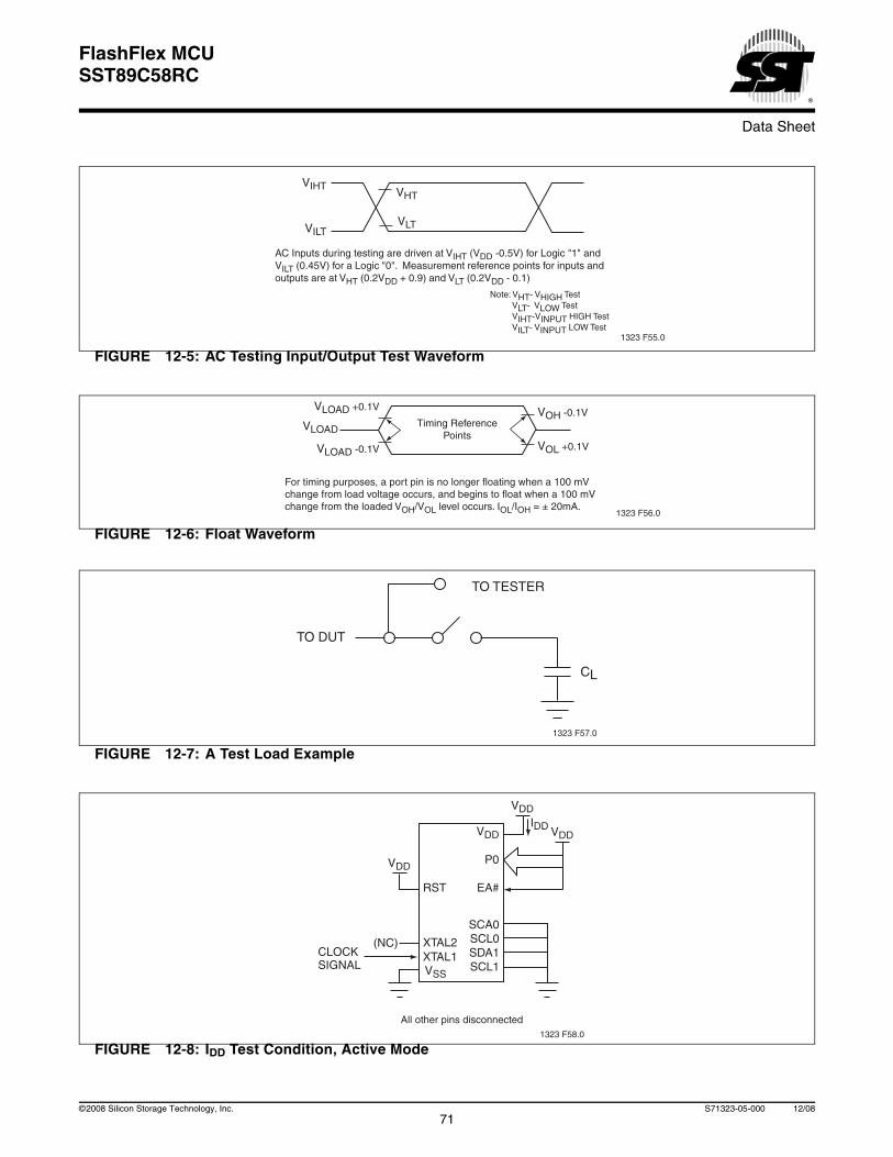
Data Sheet
FlashFlex MCUSST89C58RC
FIGURE 12-5: AC Testing Input/Output Test Waveform
FIGURE 12-6: Float Waveform
FIGURE 12-7: A Test Load Example
FIGURE 12-8: IDD Test Condition, Active Mode
VLT
AC Inputs during testing are driven at VIHT (VDD -0.5V) for Logic "1" and VILT (0.45V) for a Logic "0". Measurement reference points for inputs and outputs are at VHT (0.2VDD + 0.9) and VLT (0.2VDD - 0.1)
VHTVIHT
VILT
1323 F55.0
Note: VHT- VHIGH Test VLT- VLOW Test VIHT-VINPUT HIGH Test VILT- VINPUT LOW Test
For timing purposes, a port pin is no longer floating when a 100 mVchange from load voltage occurs, and begins to float when a 100 mV change from the loaded VOH/VOL level occurs. IOL/IOH = ± 20mA.
VLOAD +0.1V
VLOAD -0.1V
VOH -0.1VTiming Reference
PointsVOL +0.1V
VLOAD
1323 F56.0
1323 F57.0
TO TESTER
TO DUT
CL
VDD
VDD
VDD
VDD
P0
EA#RST
XTAL2(NC)CLOCKSIGNAL
All other pins disconnected
XTAL1
1323 F58.0
VSS
IDD
SCA0SCL0SDA1SCL1
71©2008 Silicon Storage Technology, Inc. S71323-05-000 12/08
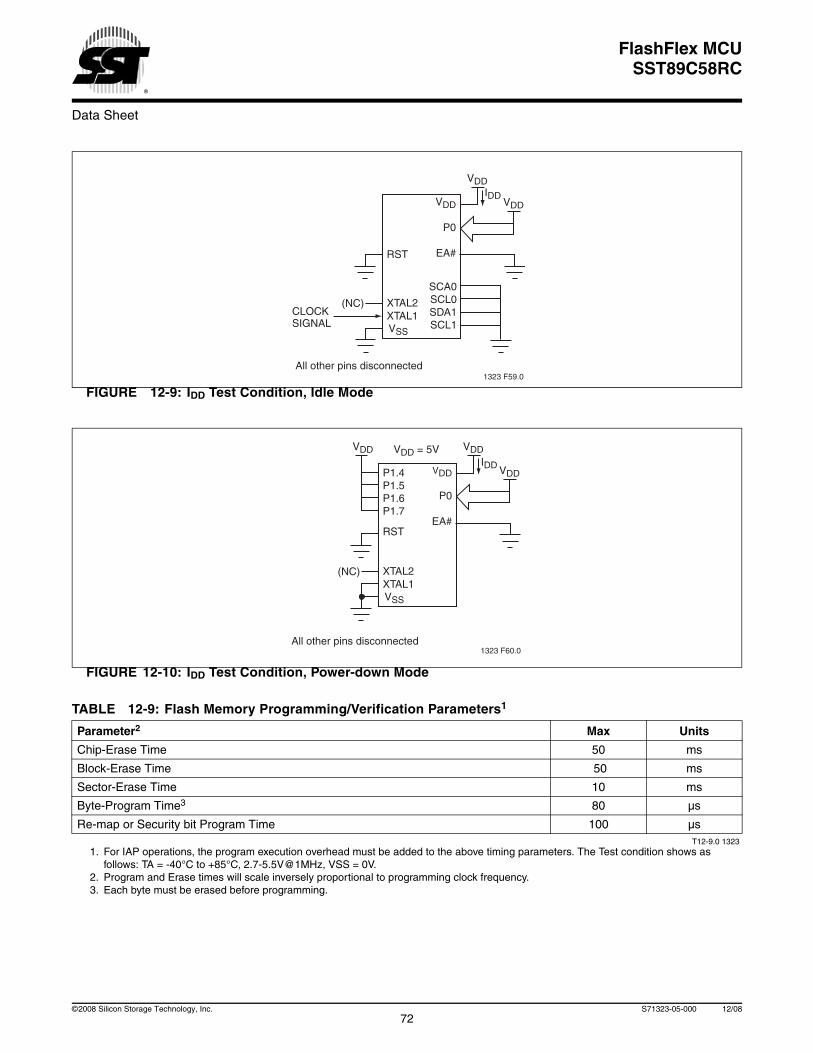
Data Sheet
FlashFlex MCUSST89C58RC
FIGURE 12-9: IDD Test Condition, Idle Mode
FIGURE 12-10: IDD Test Condition, Power-down Mode
VDD
VDD
VDD
P0
EA#RST
XTAL2(NC)CLOCKSIGNAL
All other pins disconnected
XTAL1
1323 F59.0
VSS
IDD
SCA0SCL0SDA1SCL1
TABLE 12-9: Flash Memory Programming/Verification Parameters1
1. For IAP operations, the program execution overhead must be added to the above timing parameters. The Test condition shows as follows: TA = -40°C to +85°C, 2.7-5.5V@1MHz, VSS = 0V.
Parameter2
2. Program and Erase times will scale inversely proportional to programming clock frequency.
Max Units
Chip-Erase Time 50 ms
Block-Erase Time 50 ms
Sector-Erase Time 10 ms
Byte-Program Time3
3. Each byte must be erased before programming.
80 µs
Re-map or Security bit Program Time 100 µsT12-9.0 1323
VDD
VDDVDD
VDD
P0
EA#RST
P1.4P1.5P1.6P1.7
XTAL2(NC)
All other pins disconnected
XTAL1
1323 F60.0
VSS
IDD
VDD = 5V
72©2008 Silicon Storage Technology, Inc. S71323-05-000 12/08
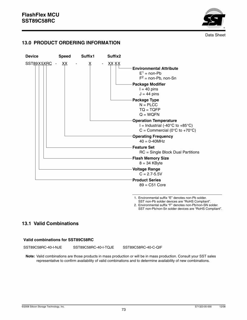
Data Sheet
FlashFlex MCUSST89C58RC
13.0 PRODUCT ORDERING INFORMATION
13.1 Valid Combinations
Note: Valid combinations are those products in mass production or will be in mass production. Consult your SST sales representative to confirm availability of valid combinations and to determine availability of new combinations.
Device Speed Suffix1 Suffix2
SST89X5XRC - XX - X - XX XXEnvironmental Attribute
E1 = non-PbF2 = non-Pb, non-Sn
Package ModifierI = 40 pinsJ = 44 pins
Package TypeN = PLCCTQ = TQFPQ = WQFN
Operation TemperatureI = Industrial (-40°C to +85°C)C = Commercial (0°C to +70°C)
Operating Frequency40 = 0-40MHz
Feature SetRC = Single Block Dual Partitions
Flash Memory Size8 = 34 KByte
Voltage RangeC = 2.7-5.5V
Product Series89 = C51 Core
1. Environmental suffix “E” denotes non-Pb solder. SST non-Pb solder devices are “RoHS Compliant”.
2. Environmental suffix “F” denotes non-Pb/non-SN solder. SST non-Pb/non-Sn solder devices are “RoHS Compliant”.
Valid combinations for SST89C58RC
SST89C58RC-40-I-NJE SST89C58RC-40-I-TQJE SST89C58RC-40-C-QIF
73©2008 Silicon Storage Technology, Inc. S71323-05-000 12/08
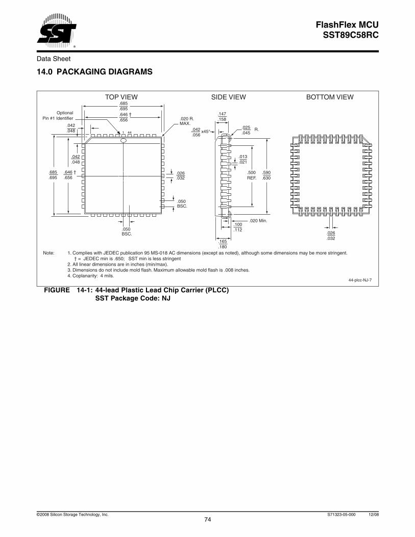
Data Sheet
FlashFlex MCUSST89C58RC
14.0 PACKAGING DIAGRAMS
FIGURE 14-1: 44-lead Plastic Lead Chip Carrier (PLCC) SST Package Code: NJ
.025
.045
.013
.021
.590
.630
.100
.112
.020 Min.
TOP VIEW SIDE VIEW BOTTOM VIEW
1 44
.026
.032
.500REF.
.165
.180
44-plcc-NJ-7
Note: 1. Complies with JEDEC publication 95 MS-018 AC dimensions (except as noted), although some dimensions may be more stringent. † = JEDEC min is .650; SST min is less stringent 2. All linear dimensions are in inches (min/max). 3. Dimensions do not include mold flash. Maximum allowable mold flash is .008 inches. 4. Coplanarity: 4 mils.
.050BSC.
.050BSC.
.026
.032
.042
.056
.646 †
.656
.042
.048
.042
.048
OptionalPin #1 Identifier
.646 †
.656.685.695
.685
.695
.020 R.MAX.
.147
.158
R.x45°
74©2008 Silicon Storage Technology, Inc. S71323-05-000 12/08
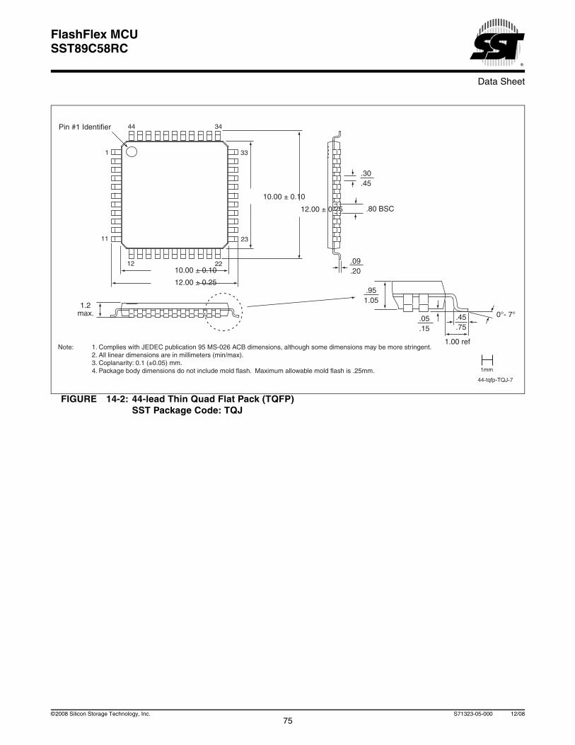
Data Sheet
FlashFlex MCUSST89C58RC
FIGURE 14-2: 44-lead Thin Quad Flat Pack (TQFP)SST Package Code: TQJ
Note: 1. Complies with JEDEC publication 95 MS-026 ACB dimensions, although some dimensions may be more stringent.2. All linear dimensions are in millimeters (min/max).3. Coplanarity: 0.1 (±0.05) mm.4. Package body dimensions do not include mold flash. Maximum allowable mold flash is .25mm.
44-tqfp-TQJ-7
.45
.75
10.00 ± 0.10
12.00 ± 0.25
1.00 ref
0°- 7°
1
11
33
23
12 22
44 34
1.2max.
.951.05
.05
.15
Pin #1 Identifier
.30
.45
.09
.20
.80 BSC12.00 ± 0.25
10.00 ± 0.10
1mm
75©2008 Silicon Storage Technology, Inc. S71323-05-000 12/08

Data Sheet
FlashFlex MCUSST89C58RC
FIGURE 14-3: 40-Contact Very-Very-Thin Quad Flat No-lead (WQFN)SST Package Code: QI
Note: 1. Complies with JEDEC JEP95 MO-220I, variant WJJD-5 except external paddle nominal dimensions. 2. From the bottom view, the pin #1 indicator may be either a 45-degree chamfer or a half-circle notch. 3. The external paddle is electrically connected to the die back-side and possibly to certain VSS leads. This paddle should be soldered to the PC board; it is suggested to connect this paddle to the VSS of the unit. Connection of this paddle to any other voltage potential will result in shorts and/or electrical malfunction of the device. 4. Untoleranced dimensions are nominal target dimensions. 5. All linear dimensions are in millimeters (max/min).
40-wqfn-6x6-QI-1
4.1
0.5 BSC
See notes2 and 3
Pin #1
0.300.18
0.0754.1
0.2
6.00 ± 0.10
6.00 ± 0.10 0.05 Max0.450.35
0.800.70
Pin #1
TOP VIEW BOTTOM VIEWSIDE VIEW
1mm
76©2008 Silicon Storage Technology, Inc. S71323-05-000 12/08
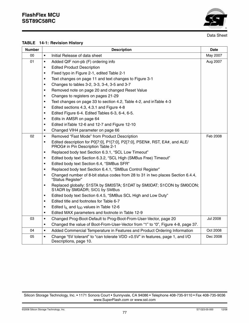
Data Sheet
FlashFlex MCUSST89C58RC
TABLE 14-1: Revision History
Number Description Date
00 • Initial Release of data sheet May 2007
01 • Added QIF non-pb (F) ordering info• Edited Product Description• Fixed typo in Figure 2-1, edited Table 2-1• Text changes on page 11 and text changes to Figure 3-1• Changes to tables 3-2, 3-3, 3-4, 3-5 and 3-7• Removed note on page 20 and changed Reset Value• Changes to registers on pages 21-29• Text changes on page 33 to section 4.2, Table 4-2, and inTable 4-3• Edited sections 4.3, 4.3.1 and Figure 4-8• Edited Figure 6-4. Edited Tables 6-3, 6-4, 6-5. • Edits in AMSR on page 64• Edited inTable 12-6 and 12-7 and Figure 12-10• Changed VIH4 parameter on page 66
Aug 2007
02 • Removed “Fast Mode” from Product Description• Edited description for P0[7:0], P1[7:0], P2[7:0], PSEN#, RST, EA#, and ALE/
PROG# in Pin Description Table 2-1• Replaced body text Section 6.3.1, “SCL Low Timeout”• Edited body text Section 6.3.2, “SCL High (SMBus Free) Timeout”• Edited body text Section 6.4, “SMBus SFR”• Replaced body text Section 6.4.1, “SMBus Control Register”• Changed number of 8-bit status codes from 28 to 31 in two places Section 6.4.4,
“Status Register”• Replaced globally: S1STA by SM0STA; S1DAT by SM0DAT; S1CON by SM0CON;
S1ADR by SM0ADR; SIO1 by SMBus• Edited body text Section 6.4.5, “SMBus SCL High and Low Duty”• Edited title and footnotes for Table 6-7• Edited IIL and IDD values in Table 12-6• Edited MAX parameters and footnote in Table 12-9
Feb 2008
03 • Changed Prog-Boot-Default to Prog-Boot-From-User-Vector, page 20• Changed the value of Boot-From-User-Vector from “1” to “0”, Figure 4-8, page 37.
Jul 2008
04 • Added Commercial Temperature in Features and Product Ordering Information Oct 2008
05 • Change “5V tolerant” to “can tolerate VDD +0.5V” in features, page 1, and I/O Descriptions, page 10.
Dec 2008
Silicon Storage Technology, Inc. • 1171 Sonora Court • Sunnyvale, CA 94086 • Telephone 408-735-9110 • Fax 408-735-9036www.SuperFlash.com or www.sst.com
77©2008 Silicon Storage Technology, Inc. S71323-05-000 12/08