Embed Size (px)
Citation preview
Flexible Electrical and Photoelectrical Artificial Synapses for Neuromorphic
Systems
Kunlong Yang
Doctoral Thesis
KTH Royal Institute of Technology Stockholm, Sweden 2018
ii
TRITA-CBH-FOU-2018:46 ISBN 978-91-7729-979-0 Akademisk avhandling som med tillstånd av Kungliga Tekniska Högskolan i Stockholm framlägges till offentlig granskning för avläggande av doktorsexamen fredagen den 31 oktober 2018 kl 9:00 i T2, Halsovagen 11C, Huddinge. © Kunlong Yang, 2018 Printed by US-AB, Stockholm
KTH Royal Institute of Technology School of Engineering Sciences in
Chemistry, Biotechnology and Health SE -141 57 Huddinge, Sweden

i
Abstract Over the past decade, the field of personal electronic systems has trended toward mobile and wearable devices. However, the capabilities of existing electronic systems are overwhelmed by the computing demands at the wearable sensing stage. Two main bottlenecks are encountered. The first bottleneck is located within the computing module, between the processing units and the memory, and is known as the von-Neumann bottleneck. The second bottleneck is located between the sensing module and the computing module of the system.
Inspired by neuromorphic computing, an architecture of the sensitive neuromorphic network (SNN) is developed as a candidate for overcoming both bottlenecks. Suitable building blocks, especially in flexible form, must be developed. In this work, starting from the demand analysis and followed by prototype development, performance optimization, and feasibility testing, two kinds of critical devices were developed for fabricating a photosensitive neuromorphic network (PSNN).
A high-performance flexible electrical artificial synapse that is based on the electron-trapping mechanism was developed. In addition to the basic memristive features, multiple kinds of synaptic plasticity were also demonstrated, which enriched the collection of possible applications. Furthermore, optimization on multiple performance metrics was easily performed using the intrinsic features and structure of the device.
A new photoelectrical artificial synapse was also realized by successfully combining light signal sensing and processing in a single synapse. A flexible dual-mode photoelectrical synapse, which fulfilled the requirements of the designed PSNN working protocol, was demonstrated. The device showed gate-tunable photomemristive features, thereby enabling its application as a photoelectrical artificial synapse.
Using the newly developed devices and the proposed network architecture, this work successfully initiated a new area of research, namely, the sensitive neuromorphic network, and provided a valid

ii
solution that addresses the current limitations of existing wearable electronic systems. Keywords: Flexible electronics, Neuromorphic network, Memristor, Electron trapping, Electrical artificial synapse, Photoelectrical artificial synapse
iii
Sammanfattning Det senaste årtiondet har inneburit en trend mot mobila och
bärbara enheter inom området personliga elektroniska system. Emellertid har processorkapaciteten hos befintliga elektroniska systemen inte hållit jämna steg med de krav som bärbara sensorer inneburit. Två flaskhalsar är speciellt tydliga. Den första flaskhalsen återfinns inom datormodulen, mellan processorenheten och minnet. Denna benämns ofta von-Neumann-flaskhalsen. Den andra flaskhalsen befinner sig mellan sensormodulen och datormodulen i systemet. Att bemästra dessa flaskhalsar skulle innebära lösningen på de utmaningar som är förknippade med registrering och bearbetning av data med nuvarande personliga elektroniska system.
Inspirerad av neuromorf databehandling, en arkitektur hos det sensoriska neuromorfiska nätverket (SNN), föreslås här en kandidat till lösning för båda flaskhalsarna. De lämpliga byggstenarna, särskilt i flexibel form, måste utvecklas. I det här arbetet, som tar sin utgångspunkt i behovsanalys, följt av prototyputveckling, prestationsoptimering och genomförbarhetsprovning utvecklades två typer av kritiska enheter.
En högpresterande flexibel elektronisk konstgjord synaps baserad på mekanismen electron-trapping utvecklades. Förutom de grundläggande memristiva egenskaperna, uppnås också synaptisk plasticitet, något som markant ökar antalet möjliga tillämpningar. Dessutom är det enkelt att optimera flertalet prestandamått med hjälp av enhetens inbyggda funktion och struktur.
Dessutom realiserades en ny fotoelektrisk artificiell synaps som kombinerar registrering och bearbetning i en enda synaps. En flexibel dual-mode fotoelektrisk synaps, som uppfyllde de specifika kraven i det aktuella SNN-protokollet, har demonstrarats. Enheten uppvisade gate-tunable foto-memristiva funktioner, vilket möjliggör att den kan fungera som en fotoelektrisk artificiell synaps.
Med hjälp av de nyutvecklade enheterna och den föreslagna nätverksarkitekturen initierar detta arbete på ett lyckosamt sätt ett helt nytt område, det sensoriska neuromorfiska nätverket, och

iv
tillhandahåller en fungerande lösning för att hantera nuvarande begränsning hos befintliga bärbara elektroniska system.
v
Acknowledgements First, I would like to express my sincerest gratitude to my
supervisors, Prof. Fernando Seoane and Prof. Lirong Zheng. Fernando guided and supported me during my whole PhD study and inspired me by setting an excellent example as an academic researcher. Lirong expanded my vision in science through his broad knowledge and prospective insights and helped me get started with this exciting research topic. I am also grateful for his support in terms of scientific resources and his help in finishing my PhD study.
I am heartily grateful to Prof. Yiqiang Zhan, who spent a lot of time helping me with the scientific discussion and providing useful advice on my work. I could not have made it this far without his consistent guidance. I am also appreciative of Prof. Zhijun Qiu, who assisted me in the work on SWCNT FET. I thank Prof. Zhuo Zou and Dr. Jiao Wang for their great ideas and new perspectives on my work and life. I also want to thank Prof. Kaj Lindecrantz for his support and advice during my study and Dr. Geng Yang for his careful and comprehensive guidance.
I would like to express my appreciation for all the kind help and support from my friends and colleagues in ICT and STH. Special thanks to Zhiying Liu, who initiated the work on SWCNT transistors, and Yuxiang Huan, for his great advice on neuromorphic computing. Farhad Abtahi, Ke Lu and Fredrik Haggstrom also helped me with their useful experiences and advices.
The close collaboration with colleagues in Fudan University provided me with great experiences and memories. I appreciate the time that I spent with them and learned a lot with my dear colleagues.
I am especially thankful for the support from my family and friends. My parents have provided great support and guidance throughout my life. Every achievement of mine is also the result of their efforts and contributions and, thus, should be shared with them. I am appreciative of the encouragement and support from all my friends.
Finally, I would like to express my deepest gratitude to my dear colleague, my best friend, and my love, Sijian Yuan, for his significant

vi
contribution to my academic research and his selfless love for me. I feel grateful for the happiness we have shared together and wish us the best on our next journey.
Kunlong Yang August 2018, Stockholm

vii
List of Publications
List of appended papers:
Paper I. Humidity effect on photoelectrical response in photosensitive field effect transistors
K. Yang, S. Yuan, Z. Qiu, Y. Zhan, L. Zheng, F. Seoane. Under review in Organic Electronics Contributions: The author came up with the idea, planned and performed most of the experiments, analyzed the results, participated in the simulation, and wrote the manuscript.
Paper II. Voltage dependency of photoelectrical memory in photoelectrical artificial synapse
K. Yang, S. Yuan, Z. Qiu, Y. Zhan, L. Zheng, F. Seoane. Under review in IEEE Transactions on Electron Devices. Contributions: The author came up with the idea, planned and performed most of the experiments, analyzed the results, participated in the simulation, and wrote the manuscript.
Paper III. A flexible artificial synapse for neuromorphic system
K. Yang, S. Yuan, Y. Zhan, L. Zheng, F. Seoane. 2018 International Conference on Electron Devices and Solid-State Circuits (EDSSC), Shenzhen, China, 2018. Contributions: The author came up with the idea, planned and performed most of the experiments, analyzed the results, participated in the simulation, and wrote the manuscript.

viii
Paper IV. Tunable flexible artificial synapses: a new path towards a wearable electronic system
K. Yang, S. Yuan, Y. Huan, J. Wang, L. Tu, J. Xu, Z. Zou, Y. Zhan, L. Zheng, F. Seoane, Npj Flex. Electron. 2, 20 (2018). Contributions: The author came up with the idea, planned and performed most of the experiments, analyzed the results, participated in the simulation, and wrote the manuscript.
Paper V. Universal and convenient optimizing strategies for three-terminal memristors
K. Yang, Y. Huan, J. Xu, Z. Zou, Y. Zhan, L. Zheng, F. Seoane. IEEE Access, vol. 6, pp. 48815-48826, 2018. Contributions: The author came up with the idea, planned and performed most of the experiments, analyzed the results, and wrote the manuscript.
Paper VI. A photoelectrical artificial synapse for novel neuromorphic network
K. Yang, S. Yuan, Y. Zhan, L. Zheng, F. Seoane. 2018 IEEE 18th International Conference on Nanotechnology (IEEE-NANO), Cork, Ireland, 2018 Contributions: The author came up with the idea, planned and performed most of the experiments, analyzed the results, and wrote the manuscript.
Paper VII. Merged acquisition-processing system based on a photoelectrical neural network
K. Yang, S. Yuan, Y. Huan, L. Tu, J. Xu, Z. Zou, J. Wang, Y. Zhan, L. Zheng, F. Seoane. Under review in Nature Communications.
ix
Contributions: The author came up with the idea, planned and performed most of the experiments, analyzed the results, participated in the simulation, and wrote the manuscript.
Related papers not appended in this thesis:
Paper VIII. A wide-range operating synaptic device based on organic ferroelectricity with low energy consumption
L. Tu, S. Yuan, J. Xu, K. Yang, P. Wang, X. Cui, X. Zhang, J. Wang, Y. Zhan, L. Zheng. RSC Adv. 8, 26549 (2018). Contributions: The author performed part of the device fabrication and characterization, data analyzing, and wrote part of the manuscript.
Paper IX. Optimized Near-Zero Quantization Method for Flexible Memristor Based Neural Network
J. Xu, Y. Huan, K. Yang, Y. Zhan, Z. Zou and L. R. Zheng, IEEE Access, vol. 6, pp. 29320-29331, 2018. Contributions: The author performed device fabricated, characterization, and wrote part of the manuscript.


xi
List of Abbreviations and symbols

xii
Table of Content
Abstract ..................................................................................... i Sammanfattning ....................................................................... iii Acknowledgements ................................................................... v
List of Publications ...................................................................vii List of Abbreviations and symbols ............................................. xi Table of Content .......................................................................xii Chapter 1. Introduction ............................................................. 1
1.1 Background and motivation ...................................................... 1 1.1.1 Problems of existing electronic systems .................................. 1 1.1.2 Neuromorphic computing ........................................................ 3 1.1.3 Artificial synapses ..................................................................... 5 1.1.4 Motivation of the thesis work .................................................. 7
1.2 Thesis introduction ................................................................... 9 1.2.1 Objective and methodology ..................................................... 9 1.2.2 Thesis outline ......................................................................... 10
Chapter 2. Device development and working principle ............. 13 2.1 Device design ......................................................................... 13
2.1.1 Mechanism and structure ...................................................... 14 2.1.2 Materials ................................................................................ 15
2.2 Experimental approaches ....................................................... 16 2.2.1 Device fabrication .................................................................. 16 2.2.2 Device characterization .......................................................... 18 2.2.3 Simulation .............................................................................. 19
2.3 Working mechanism and influence factors .............................. 19 2.3.1 Electrical responses ................................................................ 20 2.3.2 Photoelectrical responses ...................................................... 23 2.3.3 Device improvement .............................................................. 25
Chapter 3. Electrical artificial synapses and the neuromorphic network .................................................................................. 27
3.1 Performance of artificial synapses........................................... 27
xiii
3.1.1 Memristive features .............................................................. 28 3.1.2 Synaptic plasticity and flexibility ........................................... 30
3.2 Device optimization strategies ................................................ 31 3.3 Simulated neuromorphic system............................................. 34
Chapter 4. Photoelectrical and electrical artificial synapses and the PSNN ................................................................................. 37
4.1 Working protocol of the PSNN ................................................ 37 4.2 Dual-mode photoelectrical synapse (DMPS) ............................ 39 4.3 PSNN simulation..................................................................... 42
Chapter 5. Summary of the results ........................................... 45
Chapter 6. Discussion, future work and conclusions .................. 49 6.1 Discussion .............................................................................. 49 6.2 Future work ........................................................................... 50
6.2.1 Device level ............................................................................ 50 6.2.2 System level ........................................................................... 50
6.3 Conclusions ............................................................................ 51
Reference ................................................................................ 53

Chapter 1
1
Chapter 1. Introduction
1.1 Background and motivation
1.1.1 Problems of existing electronic systems
‘Wearable’ and ‘smart’ may be the most frequently used words to describe new electronic systems in recent years. Electronic systems that are aimed at individual users have become increasingly portable during their evolution. From the old stationary PCs to laptops, smart phones and wearable devices, people desire electronic systems that provide constant assistance and improve the quality of their lives. Considering the characteristics of personal users in the wearable device market, the application scenarios are more focused on multi-input, abstract, and complex tasks, such as environment analysis, decision making, and human-machine interaction. Therefore, the requirements of the electronic system gradually shift to being more cognitive and adaptive. In comparison, the largest advantage of existing computers, which is their strong power in dealing with structural problems, is less important. [1]
To build a suitable personal electronic system, first, a high-performance computing module is necessary, which works as the ‘brain’ of the system. Second, sensing modules are needed to collect various information from the environment. The whole system should be sufficiently flexible to support long-term wear. Unfortunately, current technology cannot provide satisfactory solutions. There are bottlenecks in both the computing and sensing modules.
In the computing module, the most well-known limitation is the ‘von-Neumann bottleneck’ [2]. The von Neumann architecture has been the mainstream computing paradigm due to its wide use on
Chapter 1
2
computers. Although this architecture has brought satisfactory performance to computing systems in the past decades, its limitations are becoming increasingly prominent with the increasing performance requirements on computers. The von Neumann architecture adopts separated processing and memory units, which results in high-volume data transmission between the processing and memory blocks during operation. This effect has not been taken seriously in dealing with structural tasks such as mathematical calculations. However, for multi-input and complex real-life-related tasks, the limited data transmission speed becomes a bottleneck and restricts the performance of the computer [3].
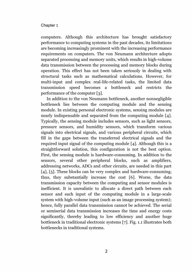
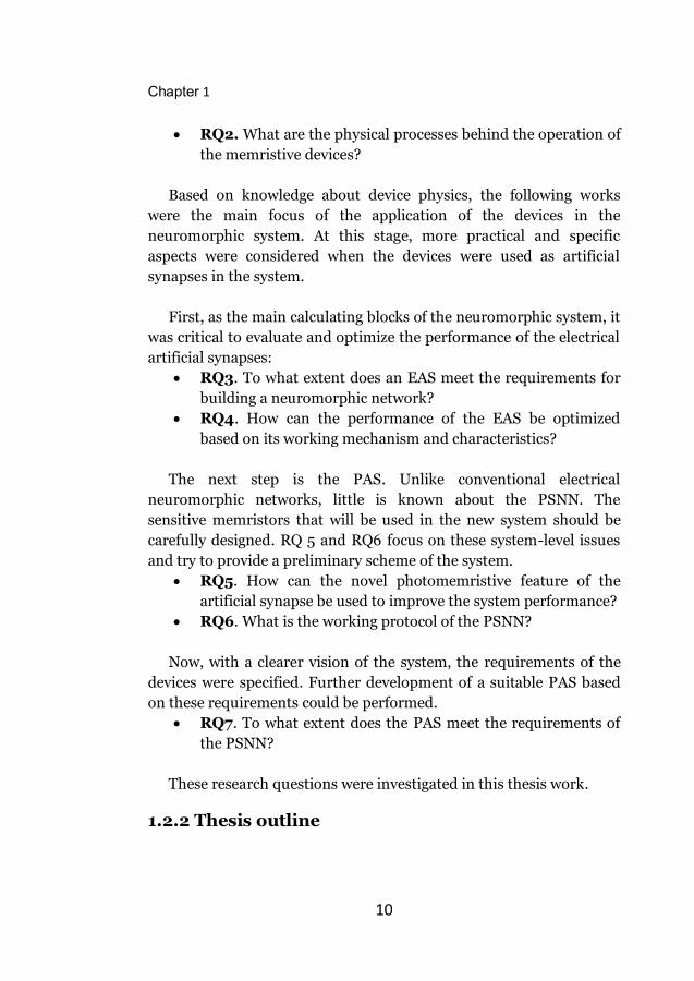
In addition to the von Neumann bottleneck, another nonnegligible bottleneck lies between the computing module and the sensing module. In existing personal electronic systems, sensing modules are nearly indispensable and separated from the computing module [4]. Typically, the sensing module includes sensors, such as light sensors, pressure sensors, and humidity sensors, which transform various signals into electrical signals, and various peripheral circuits, which fill in the gaps between the transferred electrical signals and the required input signal of the computing module [4]. Although this is a straightforward solution, this configuration is not the best option. First, the sensing module is hardware-consuming. In addition to the sensors, several other peripheral blocks, such as amplifiers, addressing networks, ADCs and other circuits, are needed in this part [4], [5]. These blocks can be very complex and hardware-consuming; thus, they substantially increase the cost [6]. Worse, the data transmission capacity between the computing and sensor modules is inefficient. It is unrealistic to allocate a direct path between each sensor and each input of the computing module in a large-scale system with high-volume input (such as an image processing system); hence, fully parallel data transmission cannot be achieved. The serial or semiserial data transmission increases the time and energy costs significantly, thereby leading to low efficiency and another huge bottleneck in traditional electronic systems [7]. Fig. 1.1 illustrates both bottlenecks in traditional systems.

Chapter 1
3
The extra challenge that is imposed by the flexibility requirement should also be considered. Since flexible devices have a shorter history, their performance is not as good compared to rigid devices, especially the well-developed silicon devices. Determining how to break through the two bottlenecks in the framework of flexible electronics is the main problem that we are currently facing.
Various actions have been taken that focus on these issues. To overcome the restrictions that are imposed by the separation of the sensing and computing modules, using a different sensing module architecture may help relieve the pressure (e.g., using CMOS sensors instead of CCD sensors to increase the speed of signal transition); however, few revolutionary changes have been made so far [8]. More work has been done on the computing module to break through the von Neumann bottleneck and increase the performance. Researchers have tried to find solutions via various approaches, from the software to the hardware and from the device to the system architecture. Among these, neuromorphic computing has been considered a promising solution.
1.1.2 Neuromorphic computing
Recently, a new candidate has stood out for its remarkable potential in breaking through the von Neumann bottleneck: brain-inspired, or neuromorphic, computing [9]–[11].
Comparing to computers, the human brain shows exceptional advantages, especially in dealing with complex, cognitive tasks [3].
Figure 1.1. Bottlenecks in the existing electronic systems.
X XCalculatingMemory
Sensing module
Computing module
Chapter 1
4
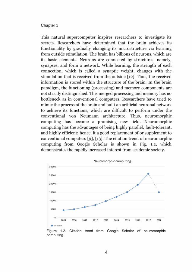
This natural supercomputer inspires researchers to investigate its secrets. Researchers have determined that the brain achieves its functionality by gradually changing its microstructure via learning from outside stimulation. The brain has billions of neurons, which are its basic elements. Neurons are connected by structures, namely, synapses, and form a network. While learning, the strength of each connection, which is called a synaptic weight, changes with the stimulation that is received from the outside [12]. Thus, the received information is stored within the structure of the brain. In the brain paradigm, the functioning (processing) and memory components are not strictly distinguished. This merged processing and memory has no bottleneck as in conventional computers. Researchers have tried to mimic the process of the brain and built an artificial neuronal network to achieve its functions, which are difficult to perform under the conventional von Neumann architecture. Thus, neuromorphic computing has become a promising new field. Neuromorphic computing has the advantages of being highly parallel, fault-tolerant, and highly efficient; hence, it a good replacement of or supplement to conventional computers [9], [13]. The citation trend of neuromorphic computing from Google Scholar is shown in Fig. 1.2, which demonstrates the rapidly increased interest from academic society.
Figure 1.2. Citation trend from Google Scholar of neuromorphic computing.
Neuromorphic computing
Chapter 1
5
So far, efforts have been made on different levels and outstanding results have already been achieved. The most exciting results might be the substantial successes on the software level [14]. Artificial neural network algorithms have demonstrated strong performance in various fields, such as image recognition, machine translation, and artificial intelligence [15]. However, these achievements were realized on conventional von Neumann computers; researchers are interested in identifying more suitable hardware on which to realize their full potential.
On the hardware level, the gradual transition from CPU to GPU, which is more suitable for parallel computing, can be viewed as a successful start [15]. In addition, more radical attempts are being made. Neuromorphic chips, such as IBM’s TrueNorth [10] and Intel’s Loihi [16], are also being developed and show very competitive performance, thereby further demonstrating the effectiveness of neuromorphic computing [10].
A new-device-based neuromorphic network is also under intensive investigation [17]–[20]. Researchers have tried to construct neuromorphic networks using novel devices. Among these works, one approach is especially attractive: the hardware implementation of neuromorphic networks using artificial synapses. As discussed earlier, the brain achieves its functioning by changing the weights of the synapses through learning; this is called synaptic plasticity. A device that can mimic the process of the synapse is of substantial importance in the hardware implementation of neuromorphic networks[21]. By using these new devices, the hardware consumption can be effectively reduced. Moreover, important features such as flexibility and functional compatibility can be integrated at the very early stage, thereby providing more possibility for this new kind of neuromorphic network.
1.1.3 Artificial synapses
The development of artificial synapses occurred in parallel with the development of system architectures and algorithms, but at a relatively slow speed because of their unique requirements. To realize

Chapter 1
6
synaptic plasticity, a device must have numerous stable, nonvolatile states that are related not only to the ongoing outside stimulation but also to the stimulation history. In other words, with the same input, the state of the device may vary because of the different stimulation histories. Existing devices do not have this feature; thus, an ensemble of several devices is used to construct an artificial synapse. A typical example is to use traditional CMOS devices to construct synapses [11], [22], [23]. However, this approach is inefficient. The situation did not improve substantially until the emergence of a new type of device: the memristor.
The concept of the memristor was first proposed by Leon Chua in the early 1970s [24] as the fourth basic circuit element (in addition to the resistor, the capacitor, and the inductance) and described the relationship between the flux and the electric charge. However, there was no hardware implementation of the memristor until Strukov et al. reformulated this relationship as a time-dependent relationship between the voltage and the current [25]: 𝑽 = 𝑹(𝒘, 𝑰)𝑰 (1)
𝒅𝒘𝒅𝒕 = 𝒇(𝒘, 𝑰) (2) The resistance of the device is time-dependent; thus, it has potential as an artificial synapse.
Since then, many memristive devices with various working mechanisms, structures, and materials have been reported [17], [18]. One of the most intensively investigated kinds is the anion/cation-based memristors, whose resistances change gradually under the electric field that is applied across them. The electric field induces the migration of anions (oxygen vacancies) [25]–[27] or cations (mental cations) [28], [29] and forms or ruptures the nanofilaments, thereby changing the resistance of the device. Although the performances of these two-terminal anion/cation-based devices have been improved substantially, there remain deficiencies, especially the unsatisfied controllability of the formation and rupture of the nanofilaments, which results in poor reliability and repeatability [30], [31]. Therefore, in addition to further optimizing filament-based memristors,
Chapter 1
7
researchers were still actively searching for other options for achieving artificial synapses. Another group of devices consists of those that adopt a three-terminal FET transistor structure. Unlike the filament-based mechanism, FET-type memristors have various working mechanisms, from electron trapping to migration of ions [32], [33]. In addition, the choices of material were more flexible and many new materials, such as graphene, MoS2, and SWCNT, are used [29], [34], [35].
To be a suitable artificial synapse, not only should the basic synaptic plasticity be realized, but various requirements on performance metrics should be fulfilled, such as the number of multilevel states, the energy consumption, the linearity, and the reliability. So far, despite active exploration, an artificial synapse with high all-around performance has yet to be identified. Problems such as lack of multilevel states, high energy consumption, and low reliability and repeatability are still the main obstacles toward the practical application of the hardware implementation of neuromorphic computers. These problems are magnified in the field of flexible artificial synapses [36]–[38]. Comparing to the situation of the rigid artificial synapses, additional efforts are needed to realize a high-performance flexible artificial synapse.
Recently, researchers have been trying to extend the memristive features to other dimensions. Instead of using the traditional electrical signal as the source of stimulation, new devices that use other kinds of signals as the stimulation source are reported. Light, temperature, and bio signals all can be used as the stimulation source [39]–[41]. The nonvolatile multilevel states in these devices change with the ongoing stimulation and history of various types of stimulation. These devices provide new models of artificial synapses; thus, they are becoming increasingly attractive. However, how to utilize these new devices remains unclear and additional investigation is necessary to explore new possible approaches [42], [43].
1.1.4 Motivation of the thesis work
Chapter 1
8
How can one break through the two bottlenecks in electronic systems based on existing achievements? As discussed above, neuromorphic computing has various advantages in dealing with the complex, parallel problems. Its features meet the requirements of personal computing systems very well; thus, it is a good candidate for breaking through the von Neumann bottleneck and realizing a high-performance personal computing system. Another advantage of a neuromorphic system is its potential compatibility with flexible electronic technologies. Typically, the performance and reliability of flexible devices are relatively low. However, the fault-tolerance of neuromorphic systems helps overcome this deficiency and provide better compatibility comparing with the traditional computing architecture. A flexible neuromorphic computer is a great candidate for future wearable personal computing systems.
However, what about the communication bottleneck between the sensing module and the computing module? Merging the sensing and computing modules would eliminate the data transmission, thereby reducing the number of communication line buses in the system. The basic strategy for realizing this merging is to use basic blocks that have both sensing and processing functions to fabricate the neuromorphic network. In this way, sensing and processing can be performed in the same network; thus, the bottleneck can be relieved, and the performance can be improved.
Therefore, the ultimate goal is to build a flexible sensing-processing merged neuromorphic network, which we call a sensitive neuromorphic network (SNN). The realization of an SNN will require tremendous effort; however, as a starting point, basic devices always lie at the top of the wish list. Suitable key components for the SNN will provide a solid foundation for the complete system.
Both electrical and sensitive artificial synapses are necessary in fabricating an SNN. The electrical artificial synapses would be mainly used to perform calculations, while the sensitive memristors would be used in the interface of the environment and remainder of the network as both sensors and calculating blocks. Theoretically, all kinds of sensitive memristors can be used to fabricate an SNN. In this thesis work, we choose to focus on photosensitive devices and a

Chapter 1
9
photosensitive neuromorphic network (PSNN) as an example implementation of an SNN.
1.2 Thesis introduction
1.2.1 Objective and methodology
The objective of this thesis work is to develop and optimize artificial synapses for a flexible photosensitive neuromorphic network.
In a PSNN, two types of artificial synapses are needed. First, a high-performance electrical flexible artificial synapse (EAS) should be developed. Second, a light-sensing function should be successfully merged into the artificial synapses to realize a photo artificial synapse (PAS). In addition, a valid working protocol for the PSNN must be designed to ensure the proper operation of the new system.
Based on the objective, several research questions are proposed and addressed during the thesis work.
Prior to any practical experiments, a comprehensive plan should be
made that considers the key aspects regarding the specific requirements. The first research question is as follows:
• RQ1. What are the main considerations in the device design for achieving key features that are required for implementing computing blocks and sensing components in a flexible neuromorphic system?
Practical fabrication and characterization of the prototype device
were performed based on the previous design. However, whether the device satisfies our requirements should be evaluated. Additionally, having a clear and comprehensive understanding of the physical mechanism behind the device was critical for the device optimization and application in the next stage. Hence, the following research question was formulated:
Chapter 1
10
• RQ2. What are the physical processes behind the operation of the memristive devices?
Based on knowledge about device physics, the following works
were the main focus of the application of the devices in the neuromorphic system. At this stage, more practical and specific aspects were considered when the devices were used as artificial synapses in the system.
First, as the main calculating blocks of the neuromorphic system, it
was critical to evaluate and optimize the performance of the electrical artificial synapses:
• RQ3. To what extent does an EAS meet the requirements for building a neuromorphic network?
• RQ4. How can the performance of the EAS be optimized based on its working mechanism and characteristics?
The next step is the PAS. Unlike conventional electrical neuromorphic networks, little is known about the PSNN. The sensitive memristors that will be used in the new system should be carefully designed. RQ 5 and RQ6 focus on these system-level issues and try to provide a preliminary scheme of the system.
• RQ5. How can the novel photomemristive feature of the artificial synapse be used to improve the system performance?
• RQ6. What is the working protocol of the PSNN?
Now, with a clearer vision of the system, the requirements of the devices were specified. Further development of a suitable PAS based on these requirements could be performed.
• RQ7. To what extent does the PAS meet the requirements of the PSNN?
These research questions were investigated in this thesis work.
1.2.2 Thesis outline
Chapter 1
11
This dissertation has been divided in six chapters. The first chapter introduces the background and motivation of the thesis work. The objective and research questions were also proposed to guide the work. The work that was carried out is presented in Chapters 2 through 4. The second chapter describes the development processes of the prototype device. The design, fabrication, and working mechanism of the prototype device are discussed prior its application as an artificial synapse. Summarized results from paper I and paper II are included in this chapter. Chapter 3 mainly focuses on the development and optimization of the EAS. The working mechanism, fabrication, and performance are described in detail and the results from paper III through paper V are introduced. Chapter 4 describes the system design and working protocol of the PSNN and the working mechanism and hardware implementation of the PAS. Chapter 5 summarizes the results from this thesis work to provide suitable answers to the research questions of this thesis. The last chapter provides an overall discussion and the general conclusions of this thesis work and outlines future work.


Chapter 2
13
Chapter 2. Device development and
working principle The objective of the thesis work is to develop artificial synapses for
flexible neuromorphic networks. There are many approaches to realizing the desired features; hence, a comprehensive analysis and proper design of the device are necessary to achieve the final goal. In addition, experimental justification of the physical process and working mechanism of the prototype device should be discussed. With this knowledge, further realization of memristive features based on the porotype device would become more convenient.
2.1 Device design As described in the objective, there are two types of artificial
synapses that are needed in the PSNN: flexible electrical and photo artificial synapses. The memristor-based device was the first choice.
Although these two devices each have their own features, they share the key fingerprint for all artificial synapses: stimulation-history-related nonvolatile resistive states. To decrease the development and manufacturing costs, the differences between the EAS and the PAS should be minimized. Hence, a proper design of the device would be beneficial in the development process. To achieve a suitable artificial synapse for a neuromorphic system, multiple requirements needed to be fulfilled. Before more detailed experiments were performed, consideration of the most important and fundamental aspects was critical at the design stage. The device should function reliably and have satisfactory compatibility for further optimization. The mechanism, structure, and material were selected based on these aspects.
Chapter 2
14
2.1.1 Mechanism and structure
For a device, the first decision should be to select the working mechanism. Existing working mechanisms include the migration of anions/cations [25], [26], polarization of the ferroelectric material [44], [45], spin-based processes [46], and trapping/detrapping of the charge carriers[35], [47], [48]. Although these mechanisms are all valid for electrical stimulations, the requirement of having both electrical and photoelectrical response narrows the range of choices. If the stimulation could influence the resistive state of a device, the change that is caused by the stimulation should be an influence factor of the device resistance. In most working mechanisms, resistance tuning in a device is realized via an intrinsic change of the materials and such a change cannot be achieved via light stimulations. However, for the carrier trapping/detrapping process, the trapping/detrapping of the charge carriers is influenced by the population of the carriers, which can be easily influenced by light with the help of photoelectrical materials. Hence, the charge carrier trapping/detrapping mechanism is a proper choice.
In choosing the mechanism, the material and structure are the other two main aspects. In trapping/detrapping memristors, a nonvolatile resistive state change is induced by trapping carriers in long-lifetime traps [35], [47], [48]. The origins of traps are various; however, one of the most effective source of traps is the interface states [49]. Thus, the field-effect transistor structure is often adopted in trapping/detrapping memristors for the large interface trapping state population. In addition, there are three terminals in the FET structure; however, typically, only two of them are used to provide effective signals. The extra terminal offers additional freedom to control the working states of the device; thus, it can be utilized to realize more functions.
In addition, the input and the output of the device should be defined. For the EAS, the input stimulation should be an electronic signal, and for the PAS, a light signal should be the stimulation source. The other aspect is the output of the device. In the electrical neuromorphic system, the resistance of the artificial synapses acts as a

Chapter 2
15
quantity of interest. In this case, the output signals for both kinds of artificial synapses should be electrical. Therefore, for the PAS, a more accurate name is the photoelectrical artificial synapse because the input is transformed from light signals to electrical signals by the device.
2.1.2 Materials
Many materials have been reported to have a trapping effect in FET devices. One of the most prominent phenomena that are related to carrier trapping is the hysteresis of the FETs [49], [50]. This inconsistent resistance during the forward and backward scans demonstrates the differences between states that have different stimulation histories; thus, it satisfies the main property of the memristive features. Therefore, FET with hysteresis has potential as an artificial synapse and in choosing materials, this phenomenon could be used as a criterion. In addition, the mechanism and process compatibility, cost, and reliability are critical influence factors, which should be considered.
The most important material is the channel material. SWCNT is a satisfactory option. Semiconductor SWCNT has excellent electrical and mechanical properties and is relatively mature for bulk production; thus, it is a very competitive candidate [51]. Prominent hysteresis was reported previously [49], [52]. In the SWCNT FET structure, the hysteresis is rooted in the electron trapping that is induced by the electrochemical reaction between the SWCNT and the H2O/O2 redox couples [53]–[55]. Hence, the source of the trapping states exists stably in the environment, which provides a reliable origin of the memristive features.
For the photoelectrical properties, more requirements should be considered. Although the SWCNT has photoelectrical response in a specified wavelength range [56]–[58], for better absorption and a more controllable light wavelength range (more sensitive to the specified wavelength range), another photoelectrical material should be used as a companion. Organic semiconductor F8T2 was selected as another ingredient of the channel material for its relatively good

Chapter 2
16
photoelectrical properties and environmental endurance [53], [59], [60]. Other advantages such as assisting the separation of photoinduced electrons and holes, better film-formation properties, and better dispersion of SWCNTs, would also improve the device performance. However, comparing to SWCNT, F8T2 has problems with environmental stability. Theoretically, F8T2 can be replaced by another photoelectrical material without jeopardizing its main memristive features; however, more detailed work should be done in the future.
SWCNT/F8T2 composite was selected as the channel material. This composite fulfills the requirements of having memristive features and high flexibility, being easy to prepare and of low cost, and having relatively good endurance.
Other materials, such as substrate, dielectric, and electrode materials, also needed to be selected. Polyimide was chosen for use as the substrate because of its excellent physical and chemical properties [61], [62] and Au was selected as the electrode material for better carrier injection into the SWCNTs. For the dielectric material, crossed-linked PVP, which is a widely used flexible dielectric material, was initially used for the prototype device [63], [64].
At this point, the device was properly designed. Next, several prototypes were fabricated and characterized.
2.2 Experimental approaches
2.2.1 Device fabrication
The fabrication of the FET can be divided into 5 steps; each step corresponds to the fabrication of a single layer:
1. Cleaning of the substrate. First, 75-μm-thick polyimide (DuPont Kapton) substrate was cleaned via ultrasound cleaning in ethanol to remove dusts and organic contaminations.
2. Definition and fabrication of the gate electrode. The gate electrode region was exposed by photo lithography. Then,

Chapter 2
17
thermal evaporation was used to prepare a 50 nm Au (Sigma Aldrich) layer on top of a 5 nm Cr (Sigma Aldrich) adhesion layer. The substrate was immersed in acetone to perform the lift-off process, in which the unwanted metal film was exfoliated with the photoresist film and only the metal on the exposed gate region could be reserved.
3. Fabrication of the dielectric layer. The cross-linked PVP was dissolved in PGMEA (Sigma Aldrich), together with the crosslinking agent PMF (Sigma Aldrich). The concentration and proportion of materials were varied in the experiments as parameters. The solution was spin-coated on top of the gate electrode, followed by an annealing process in N2 atmosphere.
4. Definition and fabrication of the source/drain electrode. The same process as the gate electrode fabrication process was adopted to define and fabricate the source/drain electrodes. The source drain electrodes were also Cr/Au electrodes with the same parameters as the gate electrode.
5. Definition and fabrication of the channel material. Since many devices were fabricated on a single substrate, proper isolation among devices was necessary. To achieve that, the channel regions were defined by exposing windows on a photoresist layer via photolithography prior to the deposition of the channel material. The channel material, namely, SWCNT/F8T2 composite, was prepared by dispersing SWCNTs (NanoIntegris, 99% semiconducting) in the F8T2 (Lumtec) solution in toluene (Sigma-Aldrich) (0.2 mg/mL). Then, the substrate was immersed in the solution for a specified time for channel thin-film deposition. After the deposition, the protective photoresist was eliminated by immersing the device in the toluene for 5 seconds. This process should quickly decrease the damage of the channel material.
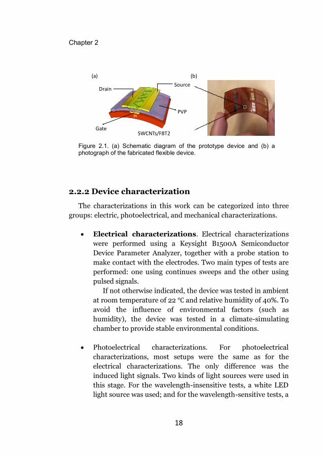
Then, the devices were characterized in the atmosphere
without further passivation. Fig. 2.1 shows a schematic diagram and photograph of the fabricated flexible device.
Chapter 2
18
2.2.2 Device characterization
The characterizations in this work can be categorized into three groups: electric, photoelectrical, and mechanical characterizations.
• Electrical characterizations. Electrical characterizations
were performed using a Keysight B1500A Semiconductor Device Parameter Analyzer, together with a probe station to make contact with the electrodes. Two main types of tests are performed: one using continues sweeps and the other using pulsed signals.
If not otherwise indicated, the device was tested in ambient at room temperature of 22 ℃ and relative humidity of 40%. To avoid the influence of environmental factors (such as humidity), the device was tested in a climate-simulating chamber to provide stable environmental conditions.
• Photoelectrical characterizations. For photoelectrical
characterizations, most setups were the same as for the electrical characterizations. The only difference was the induced light signals. Two kinds of light sources were used in this stage. For the wavelength-insensitive tests, a white LED light source was used; and for the wavelength-sensitive tests, a
Figure 2.1. (a) Schematic diagram of the prototype device and (b) a photograph of the fabricated flexible device.
PI
Gate
Drain
SWCNTs/F8T2
PVP
Source
(a) (b)
Chapter 2
19
group of quasi-monochromic LEDs were used to provide light with various wavelengths. The signal intensity and shape can be tuned by an external control signal, which was also provided by B1500A and can be easily synchronized with the electrical input signals.
• Mechanical characterizations. The mechanical test was mainly
performed to demonstrate the flexibility of the device. The substrate was fixed on the surfaces of cylinders with various radii. In this way, various bending radii were set for the tests. The substrate was repeatedly bended between the flat state (0 bending radius) and the bending state (the bending radius was set by the cylinder). Then, electrical and photoelectrical tests were performed under the bending and flat states.
2.2.3 Simulation
All simulation works in this thesis were performed using MATLAB. All codes were developed from scratch, without using any specially dedicated library. Two kinds of simulations were performed: the simulation of physical processes and the functioning of the neuromorphic network. The simulation results, together with the experimental data, support the assumed physical processes.
Then, these results were analyzed to clarify the physical processes
in the prototype device.
2.3 Working mechanism and influence
factors As the first priority, the physical processes of the fabricated
prototype device were clarified prior its use as an artificial synapse. Information about the working mechanism and influence factors was

Chapter 2
20
necessary for understanding, predicting, and optimizing the device performance in the next stages.
As discussed in the device design section, the hysteresis of SWCNT FET was induced by long-lifetime electron trapping. The electron trapping was achieved via an electrochemical reaction between the SWCNT and the H2O/O2 redox couple:
2H2O+O2+4e-⇋4OH- (3) The trapped electrons acted as electronegative centers on the channel/dielectric interface and led to screening of the gate electric field, thereby affecting the channel current [53]–[55].
In this process, the population of the trapped electrons determined the extent of the hysteresis. There are two main factors that influence the trapped electron population. The first is the gate electric field, which is the driving force of electron transfer. The population of the transferred/trapped electrons is affected by the gate electric field because it changes the chemical potential of SWCNT. A more positive gate voltage comparing to the drain will push the reaction that is shown in (3) to the right side; thus, more electrons will be trapped [53]. The second factor was the amount of the trap source, which, in this case, was related to the H2O concentration in the atmosphere and can be measured based on the relative humidity (RH).
In this section, the effects of these two factors were investigated on both electrical and photoelectrical responses. Hysteresis in the transfer characteristic was used as a tool to analyze the electrical response and the channel current under illumination was used to investigate the photoelectrical response. Detailed discussions are provided in [Paper_I] and [Paper II]. The main conclusions are summarized here for further discussion.
2.3.1 Electrical responses
The electrical performance dependency on the gate electric field and the humidity were investigated. During testing, the source/drain voltage was fixed as -10 V and the gate voltage was swept to observe the differences. For each sweep, the gate voltage started from a large

Chapter 2
21
negative voltage, scanned to a large positive voltage, and returned to the starting negative voltage.
The transfer characteristic loop was obtained. It shows a clear hysteresis in the anticlockwise direction. According to the previous reports, an anticlockwise hysteresis typically indicates a trap-related source, which satisfies our assumption [52]. Then, the sweeping range and speed were adjusted. Surprisingly, the direction of the hysteresis changed from anticlockwise to clockwise with a more negative staring voltage (Fig. 2.2 (a)) and a slower sweeping speed (Fig. 2.2 (b)). To further investigate the mechanism behind this phenomenon, the influence of the other factor, namely, the humidity, was also characterized.
Then, the device was tested under other RH conditions. A hysteresis direction change was also observed in the experiment. Under low humidity, the hysteresis was anticlockwise. With increased RH, the hysteresis loop initially twisted and subsequently became directed clockwise (Fig. 2.3). According to the direction change, more than one mechanism existed in the prototype device. Evidence was obtained that the clockwise hysteresis loop was due to the polarization of the PVP dielectric layer [65], [66].
Figure 2.2 Change of the hysteresis direction under (a) a different starting sweep point and (b) three sweep speeds. The figures are adapted from paper I.
-20 -15 -10 -5 0 5 10 15 20 25
1E-10
1E-9
1E-8
1E-7
1E-6
abs I
ds (A
)
Vg (V)
1s 500ms 100ms
-40 -30 -20 -10 0 10 20 30 401E-10
1E-9
1E-8
1E-7
1E-6
1E-5
abs I
ds (A
)
Vg (V)
clockwise anticlockwise
(a) (b)

Chapter 2
22
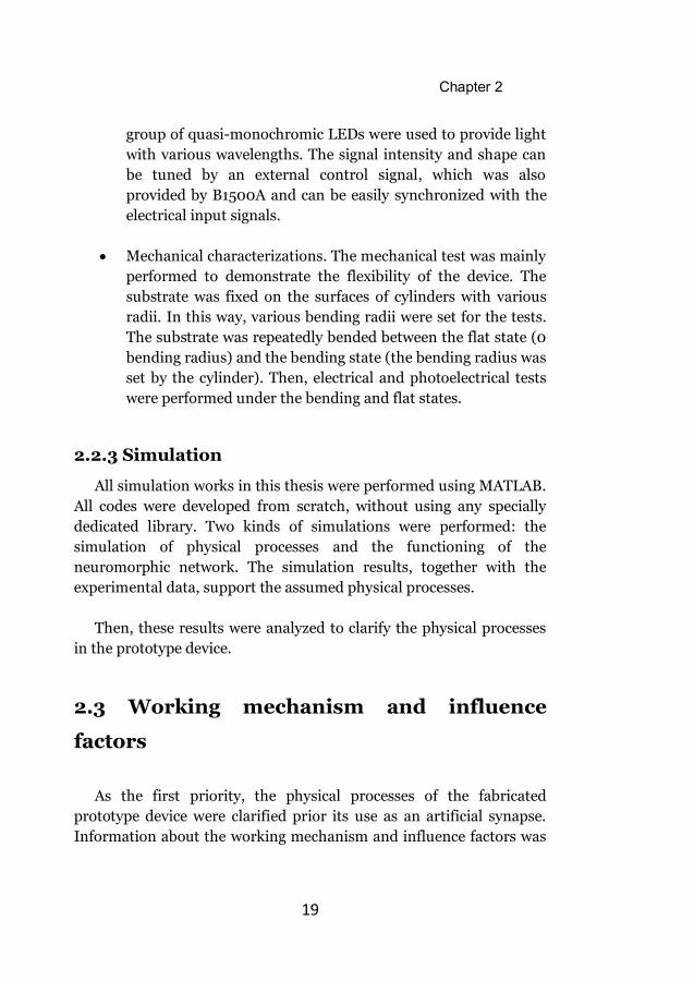
The electron trapping and the dielectric polarization had
distinguishable features. Fig. 2.4 shows schematic diagrams of the two mechanisms. The influences of various operations on these two processes were analyzed. Considering the different responses to the scan speed and scan range, the coexistence of electron trapping and dielectric polarization can be confirmed. In addition, the humidity affected the device properties through its direct influence on the degree of dielectric polarization [67]. Based on these results, the observed phenomenon can be explained:
The superposition of electron trapping and dielectric polarization determined the total hysteresis. These two processes have opposite effects and the distributions of the two processes have different trends regarding the humidity change (the proportion of the trapping hysteresis decreased with higher RH, while that of the polarization hysteresis increased). Under low RH, the carrier trapping was the leading process; thus, anticlockwise hysteresis was observed. In contrast, under high RH, the polarization process was dominant and clockwise hysteresis was observed.
Figure 2.3 Change of the hysteresis direction under various values of RH. The figure was adapted from Paper I.
-40 -30 -20 -10 0 10 20 30 40
1E-10
1E-9
1E-8
1E-7
1E-6
1E-5
abs I
ds (A
)
Vg (V)
20% 30% 50% 70% 90%
Chapter 2
23
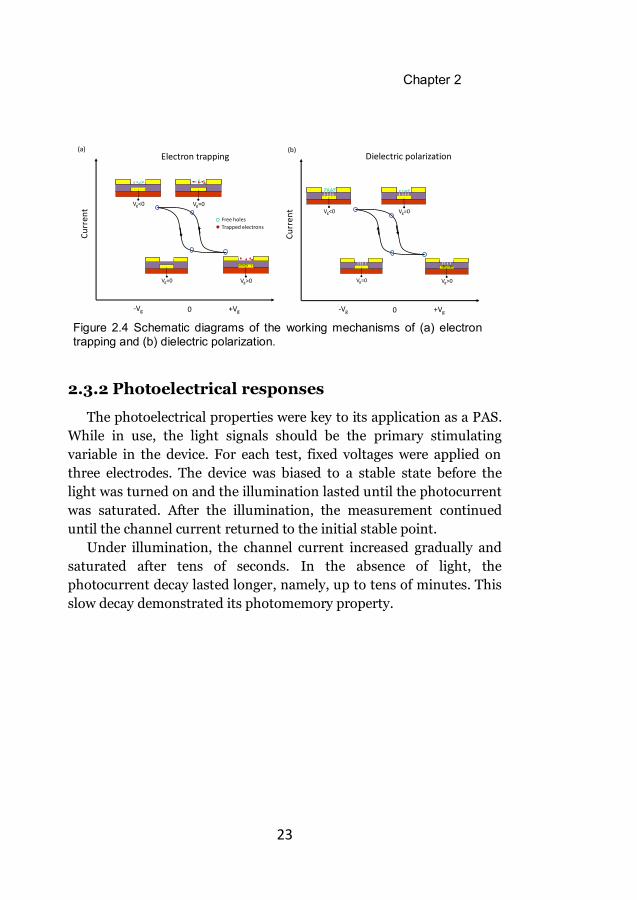
2.3.2 Photoelectrical responses
The photoelectrical properties were key to its application as a PAS. While in use, the light signals should be the primary stimulating variable in the device. For each test, fixed voltages were applied on three electrodes. The device was biased to a stable state before the light was turned on and the illumination lasted until the photocurrent was saturated. After the illumination, the measurement continued until the channel current returned to the initial stable point.
Under illumination, the channel current increased gradually and saturated after tens of seconds. In the absence of light, the photocurrent decay lasted longer, namely, up to tens of minutes. This slow decay demonstrated its photomemory property.
Figure 2.4 Schematic diagrams of the working mechanisms of (a) electron trapping and (b) dielectric polarization.
Electron trapping Dielectric polarization(b)(a)
+Vg-Vg 0
Current
- - - - -
Vg<0 Vg=0
Vg=0 Vg>0
+��+�+��+
+Vg-Vg 0
Current
- - - - -
Vg<0
Vg=0
Vg=0
+�+�+ +
Vg>0
Free holes
Trapped electrons

Chapter 2
24
First, the origin of the photocurrent was investigated. According to the results, the light was mainly absorbed by F8T2. Therefore, further possibility of changing the device’s photoelectrical properties by changing the photoelectrical material without jeopardizing the main photomemory effect was offered. The increased current was induced through the carrier trapping instead of the direct separation of excitons.
Similarly, the dependency of this photoelectrical response on the gate voltage and the humidity was tested. The results demonstrated that the photocurrent decayed faster under higher gate voltage and higher humidity, whereas the saturated photocurrent was smaller. Fig. 2.5 shows these results. The decay speed and the saturated photocurrent were both related to the detrapping of electrons. Similar to the discussion of the electrical properties, an explanation of the photoelectrical properties could be formulated.
According to classical indirect recombination theory, the recombination rate of photoinduced electrons and holes depends on several factors, among which the trap state energy level in the bandgap has a strong influence on the recombination process. The previous discussion suggested that the gate voltage would affect the energy alignment between the trap states and the SWCNT band and, thus, gate-voltage dependency would occur. In contrast, the humidity would aggravate the polarization of the PVP dielectric and further
Figure 2.5 Dependency of the photoelectrical response on (a) the gate voltage and (b) the humidity. The figures were adapted from paper I & paper II.
Chapter 2
25
change the effective gate electric field, thereby also changing the positions of the trap states. The simulation results of the processes well agreed with the experimental results, thereby supporting this model. More detailed discussions can be found in [Paper I] and [Paper II].
2.3.3 Device improvement
The results that are discussed above demonstrated that in addition to electron trapping, the dielectric polarization plays an important role in the operation of the prototype device. Since the existence of polarization weakens the trapping effect and constitutes a nonnegligible proportion of the total effect, the long-term memory of the stimulation is jeopardized. In addition, the sensitivity to environmental conditions decreases the reliability and stability of the device. Prior to more detailed characterizations regarding the potential application of this model as an artificial synapse, these issues must be clarified.
The strategy was to maximize the proportion of the trapping effect. For that, two approaches could be adopted:
1.- Increase the intensity of the trapping; 2.-Decrease the intensity of the dielectric polarization. Since the concentration of H2O/O2 on the dielectric/channel
interface is crucial for electron trapping, a hydrophilic material would increase the population of the desired water molecules. To achieve better performance, a thin Al2O3 film (10 nm) that was prepared via ALD was used as the reformative dielectric layer. Al2O3 has negligible polarization and is hydrophilic. Additionally, compared with most of the polymer dielectrics that were prepared via the solution process, the Al2O3 thin film has advantages in terms of thickness and compactness; thus, it shows increased reliability and decreased energy consumption.
In the improved device, the dependency on the humidity was substantially inhibited. The anticlockwise hysteresis was more prominent and the decay time for the photocurrent was substantially
Chapter 2
26
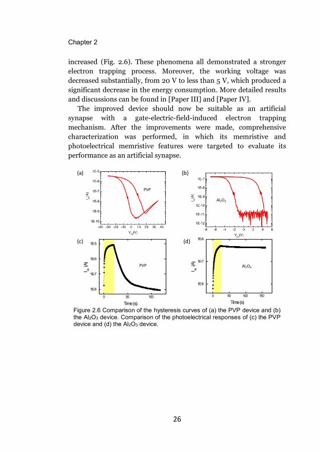
increased (Fig. 2.6). These phenomena all demonstrated a stronger electron trapping process. Moreover, the working voltage was decreased substantially, from 20 V to less than 5 V, which produced a significant decrease in the energy consumption. More detailed results and discussions can be found in [Paper III] and [Paper IV].
The improved device should now be suitable as an artificial synapse with a gate-electric-field-induced electron trapping mechanism. After the improvements were made, comprehensive characterization was performed, in which its memristive and photoelectrical memristive features were targeted to evaluate its performance as an artificial synapse.
Figure 2.6 Comparison of the hysteresis curves of (a) the PVP device and (b) the Al2O3 device. Comparison of the photoelectrical responses of (c) the PVP device and (d) the Al2O3 device.
0 50 100 150
1E-8
1E-7
1E-6
I ds (A
)
Time (s)
Al 2O3
0 50 100
1E-8
1E-7
1E-6
1E-5
I ds (A
)
Time (s)
pvp
(a) (b)
(c) (d)
PVP
Al2O3
PVP Al2O3
Chapter 3
27
Chapter 3. Electrical artificial synapses
and the neuromorphic network
3.1 Performance of artificial synapses Based on the developed SWCNT FET, the next stage is the
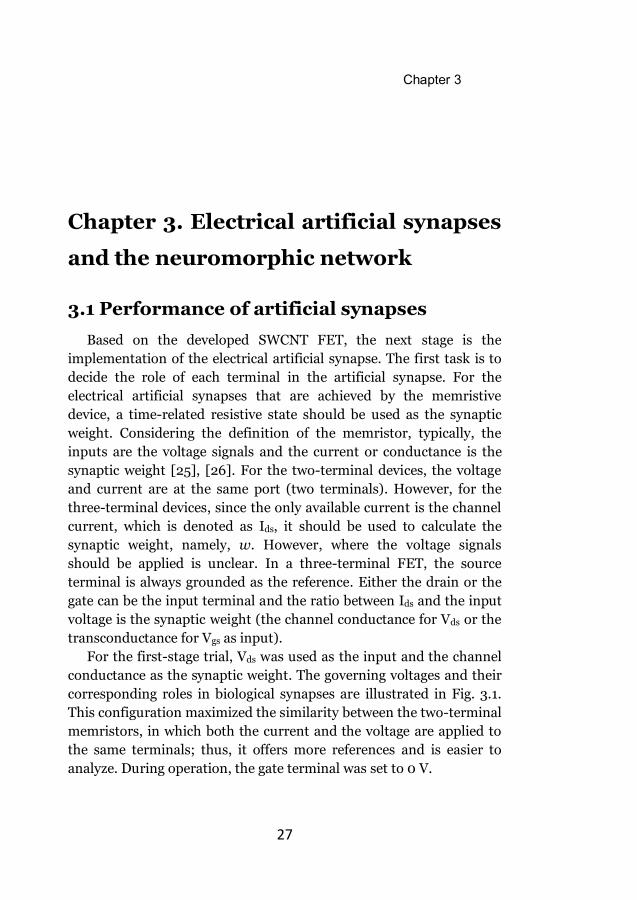
implementation of the electrical artificial synapse. The first task is to decide the role of each terminal in the artificial synapse. For the electrical artificial synapses that are achieved by the memristive device, a time-related resistive state should be used as the synaptic weight. Considering the definition of the memristor, typically, the inputs are the voltage signals and the current or conductance is the synaptic weight [25], [26]. For the two-terminal devices, the voltage and current are at the same port (two terminals). However, for the three-terminal devices, since the only available current is the channel current, which is denoted as Ids, it should be used to calculate the synaptic weight, namely, w. However, where the voltage signals should be applied is unclear. In a three-terminal FET, the source terminal is always grounded as the reference. Either the drain or the gate can be the input terminal and the ratio between Ids and the input voltage is the synaptic weight (the channel conductance for Vds or the transconductance for Vgs as input).
For the first-stage trial, Vds was used as the input and the channel conductance as the synaptic weight. The governing voltages and their corresponding roles in biological synapses are illustrated in Fig. 3.1. This configuration maximized the similarity between the two-terminal memristors, in which both the current and the voltage are applied to the same terminals; thus, it offers more references and is easier to analyze. During operation, the gate terminal was set to 0 V.
Chapter 3
28
3.1.1 Memristive features
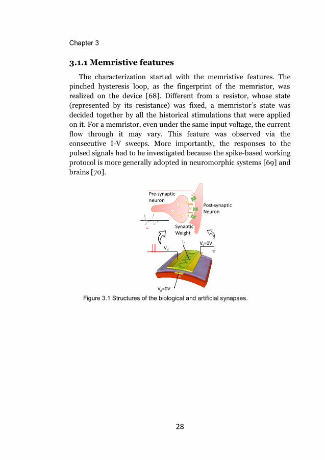
The characterization started with the memristive features. The pinched hysteresis loop, as the fingerprint of the memristor, was realized on the device [68]. Different from a resistor, whose state (represented by its resistance) was fixed, a memristor’s state was decided together by all the historical stimulations that were applied on it. For a memristor, even under the same input voltage, the current flow through it may vary. This feature was observed via the consecutive I-V sweeps. More importantly, the responses to the pulsed signals had to be investigated because the spike-based working protocol is more generally adopted in neuromorphic systems [69] and brains [70].
Figure 3.1 Structures of the biological and artificial synapses.
PI
Vg=0V
Vd
Vs=0V
Pre-synaptic
neuron
Post-synaptic
Neuron
Ic
Synaptic
Weight

Chapter 3
29
For consecutive identical pulse signals, a gradual weight change was observed. By applying signals with different polarities, bidirectional tuning of the synaptic weight was achieved. The device shows a nonlinear weight change under 100 consecutive pulsed signals. In addition, the amplitude and duration of the pulsed input induce various states. The longer time and the higher input voltage led to a more prominent weight change. These main features are shown in Fig. 3.2. These features could be easily explained by the electron-trapping mechanism that is discussed above. A positive stimulation, namely, Vgd = Vgs-Vds, moved the balance of equation (3) to the right side, thereby trapping more electrons in the dielectric/channel interface and increasing the channel current. The trapped electrons take a very long time to escape; thus, the stimulation induces stable changes of the resistive states. The intensity of the weight change was positively related to the population of the trapped electrons; thus, the duration and the intensity of the stimulation are influence factors. The electron transfer stopped when the electrochemical reaches a new
Figure 3.2 (a) The pinched hysteresis loop of the memristive device. (b) The responses to the consecutive I-V sweeps. (c) The responses to the identical pulsed signals. (d) Comparison of the current change under stimulations with different intensity and duration. The figures were adapted from Papers III & IV.
-3.0 -2.5 -2.0 -1.5 -1.0 -0.5 0.0-70-60-50-40-30-20-10
0
I ds(n
A)
Vds(V)
1st 2nd 3rd 4th
(a) (b)
-6 -4 -2 0 2 4 6-800
-400
0
400
800
I ds(n
A)
Vds(V)
12
34
+��+��+��+
Vg=0
Vd<0
SWCNT
H2O/O2
- - - -
Vg=0
Vd>0
SWCNTH2O/O2
(c) (d)

Chapter 3
30
equilibrium with the aligned Fermi levels of the SWCNTs and the redox couple, such that the channel current finally saturates.
3.1.2 Synaptic plasticity and flexibility
The memristive features are the basic functions of the artificial synapses (the nonvolatile states that are observed in the consecutive pulse stimulations), which is acceptable for the existing neuromorphic network computing protocol. However, to support more advanced applications such as online learning in the future, more synaptic plasticity should be developed. Our brains work in various ways and have different kinds of synaptic plasticity [70], [71]. In this work, other kinds of synaptic plasticity, such as STP, LTP, STDP, and SRDP, were demonstrated. These new types of synaptic plasticity are crucial for the development of the neuromorphic system [12]. For example, the STDP well supported the Hebbian learning rule [12], [23], [72], thereby offering new approaches for the neuromorphic system.
The operation of the device under flexible conditions is critical for its application in wearable systems. The device performance under various bending radii was investigated. The results demonstrated that the artificial synapse could perform properly at a bending radius that exceeds 4 mm. For smaller bending radius, slight device performance degradation would occur; however, this was reversible, and the performance could recover when the device returned to the flat state. The repeated bending tests demonstrated the high endurance of the device.
These results demonstrated that the implemented device was a
feasible candidate for implementing the flexible artificial synapses. More detailed descriptions can be found in [Paper III] and [Paper IV]. However, the observed performance can be further improved in aspects such as the energy consumption, linearity, and number of states. Our previous characterizations only changed the properties of the input signals from the two terminals while keeping the third terminal fixed. In the next stage, the use of the third terminal was investigated in detail.

Chapter 3
31
3.2 Device optimization strategies Although the implemented memristive transistor achieved the
basic requirements of the flexible artificial synapse, the performance of the artificial synapse was not ideal. The tasks for the neuromorphic network are complex and typically require a large-scale network to perform data processing. Hence, multiple performance metrics were proposed for evaluating the performance of artificial synapses in large-scale networks. The number of multilevel states, the energy consumption, the linearity, the retention time for each state, and the reliability and repeatability, among other metrics, should be considered to achieve a high-performance neuromorphic network [3]. Methods were proposed for optimizing these performance metrics. Optimizing multiple metrics was challenging. Despite significant efforts, such as inducing extra materials or structures, typically, only a few metrics could be improved significantly [18], [29], [73]. Therefore, careful design of the optimization strategy was important for achieving an effective and cost-efficient optimization.
Optimization without using an extra fabrication process is favored for its convenience, which is due to its simplicity and lower cost. In an FET, all three terminals determine together its working state and each working state has its own features. In our previous work, the three-terminal artificial synapses typically only utilized two terminals to apply effective stimulation. However, in a three-terminal artificial synapse, with two terminals working as the input terminals, the third terminal could also influence the performance. In the following work, the important role of the third terminal is investigated and two universal optimization strategies are proposed.
The artificial synapse follows all the basic rules of the field effect transistor and its performance should be highly related to the gate electric field, according to its working mechanism. With these premises, the tone of the optimization was set by tuning the effective gate electric field using various voltage configurations.
As discussed previously, both the gate/drain and the source/drain could be used as the input terminals. However, the choice between these two configurations should be made carefully the device
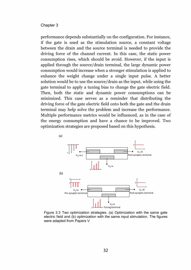
Chapter 3
32
performance depends substantially on the configuration. For instance, if the gate is used as the stimulation source, a constant voltage between the drain and the source terminal is needed to provide the driving force of the channel current. In this case, the static power consumption rises, which should be avoid. However, if the input is applied through the source/drain terminal, the large dynamic power consumption would increase when a stronger stimulation is applied to enhance the weight change under a single input pulse. A better solution would be to use the source/drain as the input, while using the gate terminal to apply a tuning bias to change the gate electric field. Then, both the static and dynamic power consumptions can be minimized. This case serves as a reminder that distributing the driving force of the gate electric field onto both the gate and the drain terminal may help solve the problem and increase the performance. Multiple performance metrics would be influenced, as in the case of the energy consumption and have a chance to be improved. Two optimization strategies are proposed based on this hypothesis.
Figure 3.3 Two optimization strategies. (a) Optimization with the same gate electric field and (b) optimization with the same input stimulation. The figures were adapted from Papers V
VS =0
Post-synaptic terminal
VD=a
Pre-synaptic terminal
VG=x
Tuningterminal
0
0
a
0
(a)
VS =0
Post-synaptic terminal
VG=x
00
a
0
VD=a-x
(b)
(a)
(b)
Chapter 3
33
The first step is to optimize the voltage distribution on all three terminals. The effects of the possible configurations on the performance metrics were investigated. During operation, a stronger stimulation would trap more electrons, thereby strengthening the synaptic features. Hence, the stimulation should induce the maximum gate electric field, which is typically determined by the thickness of the dielectric layer. With a fixed voltage Vgd, various combinations of Vgs and Vds could be selected. Fig. 3.3 (a) illustrates this strategy. Various performance metrics under 5 configurations were characterized. The results demonstrated that the Ids change that was induced by a single pulse (∆I), the dynamic range, the number of pulses in the linear region, and the power consumption were all related to the configuration, thereby demonstrating that further optimization was possible. Unfortunately, not all the performance metrics can be optimized simultaneously. With the voltage more biased to the drain terminal, the ∆I, dynamic range, linearity, and number of states were improved, but the energy consumption was increased. Thus, a trade-off between high performance and low power consumption was again observed, which is a common scenario in electronic systems. Users should choose the most suitable configuration according to the application-specific requirements.
The three-terminal device exhibits another advantage comparing with the two-terminal devices. In addition to the abovementioned optimization strategy, using the third terminal to perform fine-tuning to improve the repeatability and uniformity of the device was another option. Around a specified working point (gate electric field) and a fixed input signal amplitude, smaller changes can be made within a certain range to eliminate the variations within a single device (repeatability) or between devices (uniformity). Fig. 3.3 (b) illustrates this strategy. The performance changes were investigated with a fixed Vds and a small change in Vgs. Using the third terminal to compensate the device variation was a valid strategy for improving the repeatability and uniformity.
During the investigation, the device showed a trend that was not expected, according to the proposed working mechanism. During the fine-tuning, a small increase of the gate voltage led to a decrease of the

Chapter 3
34
∆I, which was opposite to the trend that was predicted by the gate-induced-electron trapping mechanism. Thus, other processes existed during operation and induced the observed phenomenon. Further investigation of the mechanism suggested that the channel current was also an influence factor of the performance. More detailed experiments and discussion can be found in [Paper V].
By applying these two optimization strategies to the memristive transistor, multiple performance metrics of the artificial synapse were improved substantially. The device exhibits high performance, shows a nearly linear nonvolatile resistance change under 10000 identical pulse signals within the 515% dynamic range, and has an energy consumption of as low as 45 fJ per pulse. In addition, the repeatability and uniformity were improved substantially. These results provide valid evidence of the feasibility of the proposed optimization strategy.
3.3 Simulated neuromorphic system With valid building blocks, the neuromorphic system could be
constructed. At the current stage, most neuromorphic networks adopt a layered structure. The neurons are organized as layers and each neuron is connected to every neuron in the adjacent layers via the synapses. The neurons in the neural network typically generate a nonlinear transformation between the input and the output of the layer. The input of each neuron is the weighted sum of the previous layer’s output (except the first layer).
Vi = ∑Ui*wi, (4) where V is the input of the Nth-layer neurons and U is the output of the N-1th-layer neurons. During learning, the synaptic weights, which are denoted as w, are adjusted according to the learning rules (the algorithms). The learned information is stored and reflected through the various weights and can be further used for functioning. Hence, the key to the network operation is the multilevel w. If the artificial synapse has sufficient precision and quantity of multilevel states, then successful learning could be achieved [74].
Simulated neuromorphic networks were fabricated using real data that were extracted from the experimental results. To avoid the effects
Chapter 3
35
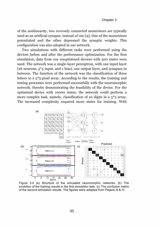
of the nonlinearity, two reversely connected memristors are typically used as an artificial synapse, instead of one [9]. One of the memristors potentiated and the other depressed the synaptic weights. This configuration was also adopted in our network.
Two simulations with different tasks were performed using the devices before and after the performance optimization. For the first simulation, data from our unoptimized devices with 500 states were used. The network was a single-layer perceptron, with one input layer (26 neurons, 5*5 input, and 1 bias), one output layer, and synapses in between. The function of the network was the classification of three letters in a 5*5-pixel array. According to the results, the training and testing processes were performed successfully with the neuromorphic network, thereby demonstrating the feasibility of the device. For the optimized device with 10000 states, the network could perform a more complex task, namely, classification of 10 digits in a 5*5 array. The increased complexity required more states for training. With
Figure 3.4 (a) Structure of the simulated neuromorphic networks. (b) The evolution of the training results in the first simulation task. (c) The confusion matrix of the second simulation results. The figures were adapted from Papers III & IV.

Chapter 3
36
adequate multilevel states, a functioning network for this task was achieved, thereby demonstrating the superior performance of the optimized artificial synapse. Fig. 3.4 illustrates the structure of the network and presents the simulation results.

Chapter 4
37
Chapter 4. Photoelectrical and
electrical artificial synapses and the
PSNN
4.1 Working protocol of the PSNN The PAS is another key component of the PSNN. Analogous to the
EAS, a device that can memorize multiple light signals in the form of stable electrical resistive states could be used as a PAS. However, the question of whether all the requirements for the PAS are fulfilled would arise. Moreover, would the PAS be just another kind of regular artificial synapse with a modified input signal form? Before answering these questions, the working protocol of the PSNN and the requirements of the photoelectrical artificial synapses should be clarified.
To realize the sensing-processing merged system, the light signals had to be the input. This characteristic led to the main difference between the use of the electrical and photoelectrical artificial synapses. In the electrical neuromorphic network, to achieve successful training, the synaptic weights had to be adjusted via electrical stimulations according to the training algorithm. The algorithm typically reflects the organization of the input, the structural information of the network, and the label that indicates the correct information of the input[74]. For the PAS, for which stimulation signal was restricted to the light input, adjusting the weights to achieve successful learning is the most important issue. Therefore, the role of the PAS in the PSNN must be designed carefully.

Chapter 4
38
The first step is to determine the location of the PAS in the network. In the commonly used neuromorphic networks, the input data are only directly used in the input layer [12]. Therefore, the proper location for the PAS should be in the input layer. Since our electrical and photoelectrical synapses are based on the same device, the fabrication process of the network can be simplified. Separate fabrication processes are not necessary, but proper shielding of light in the EAS is required for the isolation of the two kinds of synapses.
However, the synapses in the input layer still outnumbered the required sensing units (a denotes the number of input neurons and a*v the number of synapses, where v is the number of neurons in the next layer). In this case, redundant PAS weights would be modified by the light input. Therefore, the second issue is to decide how to address and modify each PAS according to the algorithm. Luckily, the photoelectrical nature of the device determines its electrical properties and it might respond to electrical signals. If the artificial synapse responds to both light and electrical signals, then each PAS could be addressed individually through the light signal from the input layer and the control signal from the second layer. In this way,
all the synaptic weights could be modified according to the algorithm. Based on the previous discussion, a preliminary design of the
PSNN was realized to construct a layerwise neuromorphic network. The synapses between the first two layers were the PASs and the remaining synapses were regular EASs. During the training stage, the
Figure 4.1 Structure of the PSNN.

Chapter 4
39
BP algorithm should be used to determine the weight change, namely, ∆w. The light input signals are applied on the presynaptic neurons (first-layer neurons) and the calculated BP signals can be applied through the postsynaptic neurons (second-layer neurons). In this way, every PAS could be individually controlled. During the testing stage, the electrical control signal should keep the weights unchanged under all light signals; otherwise, the network could not perform properly. Fig. 4.1 illustrates the structure of the PSNN.
Next, the key requirements for the PAS are clarified: First, the
device should have nonvolatile multilevel states and the number of states and the linearity should be in acceptable ranges to achieve successful functioning of the network. Second, an external electrical control on the weight changing process is necessary and a requirement of the photoelectrical artificial synapse is identified. With these requirements as targets, the SWCNT transistor was characterized to determine to what extent the requirements were fulfilled.
4.2 Dual-mode photoelectrical synapse
(DMPS) First, the stable photoelectrical multilevel states were
demonstrated. With identical consecutive light pulses, the channel current increased after each pulse and remained stable until the next signal arrived (Fig. 4.2(a)). On this basis, 10000 light pulses (0.025 μW/mm2; duration: 10 ms; frequency: 0.05 kHz) were applied to calculate the performance metrics of the devices, which might further affect the performance of the neuromorphic network. The weight change shows high linearity in the tested range; thus, it provides sufficient performance for relatively complex computations (Fig. 4.2(b)). These results were in stark contrast with various reported photoelectrical memories, which typically only have a few states and are saturated easily [42], [43], [75]. Moreover, the relationship between the photoelectrical response and the pulse duration/intensity

Chapter 4
40
was investigated. The longer and more intense the light input was, the faster the current would increase. However, larger ∆w was achieved at the price of a smaller number of states and poorer linearity; this tradeoff should be carefully evaluated during practical applications.
According to the previous investigation of the working mechanism, effective trapping of the light-generated electrons is essential for its light-memristive features. In this process, the gate electric field plays an important role in the electron trapping. A proper bias on the gate terminal would enhance the driving force of the electron trapping. Although a constant bias is applied on the device, which would lead to a state drift that is caused by the electric-driven electron trapping, the small base current in the dark states limits the electric-induced weight change. Moreover, this drift was negligible comparing to the relatively large light-induced state change. Consequently, it was safe to use the same device for both electrical and photoelectrical artificial synapses. Furthermore, the gate electric field could affect the light-induced electron trapping; hence, electrical tuning is possible, which was the special requirement of the photoelectrical artificial synapse.
Then, the potential of the gate-tuning function was demonstrated. The results demonstrated that under various gate biases, the photoelectrical responses differed. As shown in Fig. 4.3(a), the more positive the gate voltage is, the more prominent the photoinduced current change will be. This effect meets the requirement of accurate electrical tuning; consequently, it is considered a valid control method.
Figure 4.2 Channel current response for consecutive pulsed signals. (a) Long-term memory of each light pulse. (b) Response to 10000 light pulses. The figures were adapted from paper VII.
(a)
(b)(a)
(b)

Chapter 4
41
During operation, the weight update process should be controlled by both the light input and the control signal. Most algorithms required an arbitrary value of ∆w. However, this would lead to a higher demand on the electrical controllability since using different light pulses from each input signal to update the weights to their required values [9], [72] is difficult. For the PSNN, a modified BP algorithm was developed. In this new algorithm, the BP signal was binary; hence, the BP signal only provided two modes: “On” and “Hold.” In the “On” mode, the synaptic weight had a response to the input and in the “Hold” mode, the input signal could not induce changes in the synaptic weights. Thus, the demand for the abovementioned precise change according to the BP signal is lower, thereby minimizing the possibility of errors and simplifying the hardware configuration. During training, the device mode was controlled by the training algorithms; during testing, the device was set to the hold mode the entire time.
To implement this algorithm, a dual-mode photoelectrical synapse (DMPS) was needed. It was realized using the obtained photoelectrical memristive transistor. The gate-tuning function was the key to achieving the “dual-mode” of the photoelectrical synapse. Two Vg values were used for each mode. When the gate voltage Vg= 3 V, the weight change with the light signal was permitted; consequently, the device was considered to be in the “on” mode. When Vg= −3 V, the weights remained unchanged under illumination; thus, the device
Figure 4.3 (a) The gate-voltage dependency of the photoelectrical response. (b) The responses under various working modes. The figures were adapted from paper VII.
(a) (b)
(c) (d)

Chapter 4
42
operated in the “hold” mode. These two modes should work independently, which means each mode should have a unique function under both illumination and dark states. In addition, a volatile change under the hold mode was necessary for the network to realize the testing function. The characteristics of various modes are demonstrated in Fig. 4.3(b). Detailed discussions can be found in [Paper VI] and [Paper VII].
4.3 PSNN simulation To demonstrate the feasibility of the PSNN, a simulation that used
the experimental data and the designed working protocol was performed. The simulation task was handwritten digit classification in a 28*28-pixel array. The system was a two-layer neuromorphic network with 784 inputs and 10 outputs. Similar to the electrical neuromorphic networks, two devices were combined to form an artificial synapse. The Widrow–Hoff rule was first adopted to calculated the BP signal. Then, a threshold was set to binarize the BP signal. Only the BP signals that exceeded the threshold could be applied on the synapses and used for weight updating. The Modified National Institute of Standards and Technology (MNIST) database was used for the training and testing of the system [76], with 4500 patterns for training and 500 patterns for testing. This simulated PSNN obtained a recognition rate of as high as 89% within 100 epochs. Fig. 4.4 illustrates the algorithm and presents the simulation results. This simulation demonstrated the feasibility of our photoelectrical artificial network and the working protocol of PSNN.
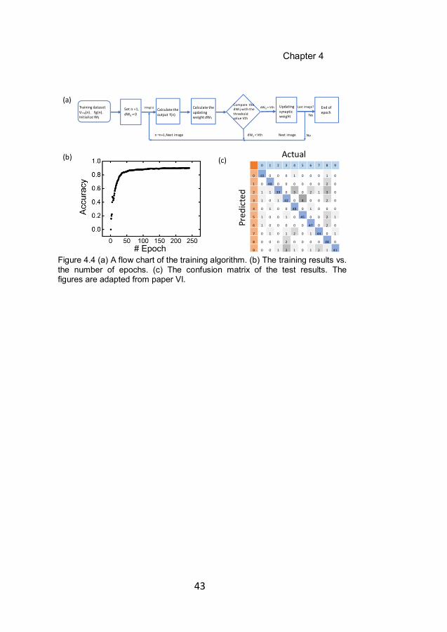
Chapter 4
43
Figure 4.4 (a) A flow chart of the training algorithm. (b) The training results vs. the number of epochs. (c) The confusion matrix of the test results. The figures are adapted from paper VI.

Chapter 5
45
Chapter 5. Summary of the results Driven by the strong desire to break through the two bottlenecks in
existing computing systems, a flexible (SNN) was designed. The SNN is based mainly on artificial synapses. The research work that was performed has been presented in the previous chapters. Now, we look back to the thesis’ research questions and the objectives, to see how the results of this work have addressed them.
• RQ1. What are the main considerations in device design for
achieving key features that are required for implementing computing blocks and sensing components in a flexible neuromorphic system?
The device design is discussed comprehensively in chapter 2.1 and
research papers III-VII. The proper working mechanism, structure, and materials are designed prior to the experimental implementation. An SWCNT/polymer-based flexible FET was designed as the prototype device for application as electrical and photoelectrical artificial synapses. Thus, this design addresses RQ1 and provides a valid benchmark for subsequent works.
• RQ2. What are the physical processes behind the operation of
the memristive devices? In Chapter 2.3 and research papers I & II, the electrical and
photoelectrical physical processes were systemically investigated in a prototype device using a PVP dielectric layer. The coexistence of electron trapping and dielectric polarization was demonstrated experimentally and via simulations. Thanks to the comprehensive understanding that was obtained from these preliminary works, a

Chapter 5
46
modified device that uses Al2O3 dielectric material was fabricated, which yielded satisfactory results as an artificial synapse. The physical processes and working mechanisms of the EAS and PAS are discussed in papers III-VII. These works successfully addressed RQ2 and set a solid foundation for further work on optimizing the EAS and PAS.
• RQ3. To what extent does an EAS meet the requirements for
building a neuromorphic network? In Chapter 3.1, basic memristive features and synaptic features of
the produced devices were demonstrated. Simulation results in chapter 3.3 also demonstrated their feasibility as artificial synapses. The performances of the unoptimized and optimized artificial synapses were demonstrated in Paper III and Paper VI, respectively. Simulated applications as building blocks in neuromorphic networks were also included. By evaluating the performance metrics of the device and the results of the simulated network, the research question can be addressed.
• RQ4. How can the performance of the EAS be optimized based
on its working mechanism and characteristics? Several possibilities are available for optimizing the performance.
In chapter 3.2, valid optimization strategies that use a three-terminal device structure were proposed for improving multiple performance metrics, such as ∆I, the dynamic range, linearity, number of states, and energy consumption. These optimization strategies require no additional fabrication processes and achieved substantial performance improvements. Hence, more complex tasks could be performed with the optimized devices, as demonstrated in Chapter 3.3. A detailed discussion was included in paper V.
• RQ5. How can the novel photomemristive feature of the
artificial synapse be used to improve the overall system performance?
Chapter 5
47
The photomemristive feature provides history-related multilevel states under the stimulation of light signals. In this way, the light signals could be sensed and processed at the same time. The implementation of the PSNN would eliminate the data acquisition and transfer costs, thereby improving the system performance. The advantages of using the photoelectrical artificial synapse to fabricate the PSNN have been discussed in Chapter 1 and were investigated in Papers VI & VII.
• RQ6. What is the working protocol of the PSNN?
In chapter 4.1, the working protocol of the PSNN was designed to
realize a sensing-processing merged neuromorphic network. A traditional layerwise network structure and modified BP algorithms were adopted to address problems in the operation of the PSNN. By answering this research question, the basic rules of the PSNN and the requirements on the photoelectrical artificial synapses were clarified. Paper VII presents a detailed discussion about the system architecture and working protocol.
• RQ7. To what extent does the PAS meet the requirements of
the PSNN? Targeting the requirements that are specified in chapter 4.1, a
hardware implementation of a photomemristive device was achieved. The device met the requirements on the number of multilevel states and linearity. More importantly, the requirement of the PSNN, which was the electrical tuning of the photosensitivity, was realized using the gate terminal of the PAS. These features made it a suitable candidate for light-sensing-based neuromorphic computing. Simulations in Chapter 4.3 also demonstrated the feasibility of the network and the device; thus, they also contributed to answering this research question. Detailed results and discussions were also included in Papers VI & VII.

Chapter 6
49
Chapter 6. Discussion, future work and
conclusions
6.1 Discussion In this thesis, flexible EAS and PAS were developed. The devices
were carefully designed. Then, the physical processes in the prototype device were systematically investigated. A successful modification of the prototype device, based on a comprehensive understanding of the mechanism, resulted in a memristive transistor, which was used as an artificial synapse. The effective electron-trapping mechanism provided reliable working conditions for both EAS and PAS. The gate terminal not only offered a competitive EAS comparing with the existing devices [36]–[38], [42], [43] but also enabled the unique functioning of the PAS. Simulation results demonstrated that the current versions of the EAS and PAS are capable of constructing neuromorphic networks for simple tasks.
However, there remain deficiencies in our artificial synapses. For example, the fabrication process still includes some steps with high cost and complexity, such as the ALD and the photolithography. It would be better for the bulk manufacturing if these processes could be replaced by simpler ones.
Further performance improvement would also be beneficial. The optimization strategies in this thesis work were based on the intrinsic features of the three-terminal device; thus, they could achieve performance improvements without changing the device structure. However, as discussed in the thesis, there were trade-offs among the performance metrics. Additionally, there are other important features that could be optimized, such as the dimension and the long-term
Chapter 6
50
endurance of the device [3]. A smaller device would increase the integration density, which is critical for large-scale systems [3]. The long-term endurance issue is mainly caused by the existence of the organic polymer [77], [78]. Although F8T2 has relatively good endurance in the ambient environment, its long-term endurance is unsatisfactory [59]. Further improvements in these aspects would relieve the stress on the system design and improve the system performance.
On the system level, there remains much work to be done. The hardware implementation of the PSNN includes various aspects. In this work, only the basic protocol and the PAS were realized. Other issues such as signal matching between various types of synapses and the layout of the network using three-terminal devices should all be addressed.
6.2 Future work
6.2.1 Device level
On the device level, optimization of the device performance and fabrication process are the main objectives for the next stage of work. To realize a more balanced device and decrease the fabrication cost, several approaches could be adopted:
• Scaling down the device dimensions for higher integration and improved device performance.
• Changing the dielectric material to simplify the fabrication method and improve the device performance. The material should have better ability to trap electrons and be fabricated at lower cost.
• Changing the organic semiconductive polymer to improve the stability and photoelectrical performance of the device.
• Developing a lower-cost fabrication process, such as printing electrodes to avoid the high cost of lithography.
6.2.2 System level
Chapter 6
51
On the system level, the hardware implementation of the PSNN is the main challenge. The hardware implementation could be divided into two stages.
First, a successful electrical neuromorphic network should be realized using the developed EAS. In this process, the modified algorithms with a binary BP signal should be adopted for further integration of the PAS. Initially, an off-line learning protocol could be used, as in our simulation. Using this approach, only the key synapse array and the stimulation source are needed for the neuromorphic system. Issues such as the system layout and the stimulation source should be carefully addressed to provide a solid foundation for the next stage. Moreover, online learning using more advanced algorithms and hardware could be investigated using the multiple synaptic plasticity that is demonstrated in this work. Regarding the scale of the system, gradually increasing the system scale via trial and error is preferred.
Furthermore, the PAS should be integrated into the fabricated electrical neuromorphic network. At this stage, the biggest challenge would be to match the synaptic weights in EAS and PAS. Different stimulation sources would induce mismatch of the synaptic weight changes during training; thus, this problem should be fixed. Similarly, step-by-step increase of the network scale and the algorithm complexity should also be performed during the development.
With the hardware implementation of the PSNN as convincing proof, the potential of the SNN would be further demonstrated.
6.3 Conclusions By addressing the research questions, the objective of the thesis
work was achieved. The PSNN was successfully designed and the critical devices for the network were fabricated. The flexible artificial synapses were realized on a memristive transistor based on the electron-trapping mechanism. Both the electrical and photo stimulations could contribute to the weight changing in the synapses, thereby successfully demonstrating the EAS and the PAS. The

Chapter 6
52
performances of the EAS and PAS were further evaluated via multiple performance metrics and the simulated neuromorphic networks.
In this way, a competitive option for future personal computing systems was provided, by taking a step away from concept and design toward practical realization and applications. There remains much work to be done to realize a PSNN in practice; however, this work would set a solid foundation for this new area.

53
Reference [1] Z. Xiao and J. Huang, “Energy-Efficient Hybrid Perovskite
Memristors and Synaptic Devices,” Adv. Electron. Mater., vol. 2, no. 7, pp. 1–8, 2016.
[2] J. Backus, “Can programming be liberated from the von Neumann style? a functional style and its algebra of programs,” Commun. ACM, vol. 21, no. 8, pp. 613–641, 1978.
[3] D. S. Jeong, K. M. Kim, S. Kim, B. J. Choi, and C. S. Hwang, “Memristors for Energy-Efficient New Computing Paradigms,” Adv. Electron. Mater., vol. 2, no. 2, pp. 1–27, 2016.
[4] R. LiKamWa, B. Priyantha, M. Philipose, L. Zhong, and P. Bahl, “Energy characterization and optimization of image sensing toward continuous mobile vision,” Proceeding 11th Annu. Int. Conf. Mob. Syst. Appl. Serv. - MobiSys ’13, p. 69, 2013.
[5] A. El Gamal and H. Eltoukhy, “CMOS Image Sensors,” Circuits Devices Mag. IEEE, vol. 21, no. 3, pp. 6–20, 2005.
[6] M. Bigas, E. Cabruja, J. Forest, and J. Salvi, “Review of CMOS image sensors,” Microelectronics J., vol. 37, no. 5, pp. 433–451, 2006.
[7] S. Mendis, S. E. Kemeny, and E. R. Fossum, “A 128x128 CMOS Active Pixel Image Sensor for Highly Integrated Imaging Systems,” pp. 2–5, 1993.
[8] R. Hain, C. J. Kahler, and C. Tropea, “Comparison of CCD, CMOS and intensified cameras,” Exp. Fluids, vol. 42, no. 3, pp. 403–411, 2007.
[9] M. Prezioso, F. Merrikh-Bayat, B. D. Hoskins, G. C. Adam, K. K. Likharev, and D. B. Strukov, “Training and operation of an integrated neuromorphic network based on metal-oxide memristors.,” Nature, vol. 521, no. 7550, pp. 61–4, May 2015.
[10] P. A. Merolla et al., “A million spiking-neuron integrated circuit with a scalable communication network and interface,” Science (80-. )., vol. 345, no. 6197, p. 668 LP-673, Aug. 2014.
[11] M. R. Azghadi, S. Moradi, and G. Indiveri, “Programmable neuromorphic circuits for spike-based neural dynamics,” 2013 IEEE 11th Int. New Circuits Syst. Conf. NEWCAS 2013, no. December 2016, 2013.
[12] G. Indiveri and S. C. Liu, “Memory and Information Processing in Neuromorphic Systems,” Proceedings of the IEEE, vol. 103, no. 8. pp. 1379–1397, 2015.
[13] J. Sawada et al., “A million spiking-neuron integrated circuit with
54
a scalable communication network and interface,” vol. 345, no. 6197, 2014.
[14] Y. LeCun, Y. Bengio, and G. Hinton, “Deep learning,” Nature, vol. 521, no. 7553, pp. 436–444, May 2015.
[15] Y. Lecun, Y. Bengio, and G. Hinton, “Deep learning,” 2015. [16] M. Davies et al., “Loihi: A Neuromorphic Manycore Processor
with On-Chip Learning,” IEEE Micro, vol. 38, no. 1, pp. 82–99, 2018.
[17] Z. Wang et al., “Memristors with diffusive dynamics as synaptic emulators for neuromorphic computing,” Nat. Mater., vol. 16, p. 101, Sep. 2016.
[18] W. Xu et al., “Organometal Halide Perovskite Artificial Synapses,” Adv. Mater., vol. 28, no. 28, pp. 5916–5922, 2016.
[19] P. Gkoupidenis, N. Schaefer, B. Garlan, and G. G. Malliaras, “Neuromorphic Functions in PEDOT:PSS Organic Electrochemical Transistors,” Adv. Mater., vol. 27, no. 44, pp. 7176–7180, 2015.
[20] L. Q. Zhu, C. J. Wan, L. Q. Guo, Y. Shi, and Q. Wan, “Artificial synapse network on inorganic proton conductor for neuromorphic systems.,” Nat. Commun., vol. 5, p. 3158, 2014.
[21] R. C. Tees, The Organization of Behaviour: A Neuropsychological Theory. Cambridge, MA, USA: MIT Press, 1961.
[22] Y. V. Pershin and M. Di Ventra, “Experimental demonstration of associative memory with memristive neural networks,” Neural Networks, vol. 23, no. 7, pp. 881–886, 2010.
[23] S. Moradi and G. Indiveri, “A VLSI network of spiking neurons with an synchronous static random access memory,” IEEE Biomed. Circuits Syst. Conf., pp. 277–280, 2011.
[24] L. O. Chua, “Memristor—The Missing Circuit Element,” IEEE Trans. Circuit Theory, vol. 18, no. 5, pp. 507–519, 1971.
[25] D. B. Strukov, G. S. Snider, D. R. Stewart, and R. S. Williams, “The missing memristor found.,” Nature, vol. 453, no. 7191, pp. 80–3, May 2008.
[26] Y. Du et al., “The resistive switching in TiO 2 films studied by conductive atomic force microscopy and Kelvin probe force microscopy,” AIP Adv., vol. 3, no. 8, p. 082107, Aug. 2013.
[27] T. Chang, S.-H. Jo, and W. Lu, “Short-Term Memory to Long-Term Memory Transition in a Nanoscale Memristor,” ACS Nano, vol. 5, no. 9, pp. 7669–7676, Sep. 2011.
[28] S. La Barbera, D. Vuillaume, and F. Alibart, “Filamentary Switching: Synaptic Plasticity through Device Volatility,” ACS Nano, vol. 9, no. 1, pp. 941–949, Jan. 2015.

55
[29] Z. Wang, L. Wang, M. Nagai, L. Xie, M. Yi, and W. Huang, “Nanoionics-Enabled Memristive Devices: Strategies and Materials for Neuromorphic Applications,” Adv. Electron. Mater., vol. 3, no. 7, 2017.
[30] R. Waser and M. Aono, “Nanoionics-based resistive switching memories.,” Nat. Mater., vol. 6, no. 11, pp. 833–40, 2007.
[31] J. J. Yang, D. B. Strukov, and D. R. Stewart, “Memristive devices for computing.,” Nat. Nanotechnol., vol. 8, no. 1, pp. 13–24, Jan. 2013.
[32] Z. Wang et al., “Memristors with diffusive dynamics as synaptic emulators for neuromorphic computing,” Nat. Mater., vol. 16, no. 1, pp. 101–108, Sep. 2016.
[33] F. Alibart et al., “A Memristive Nanoparticle/Organic Hybrid Synapstor for Neuroinspired Computing,” Adv. Funct. Mater., vol. 22, no. 3, pp. 609–616, Feb. 2012.
[34] W. Wang et al., “MoS2 memristor with photoresistive switching,” Sci. Rep., vol. 6, no. August, p. 31224, 2016.
[35] H. Tian et al., “Graphene Dynamic Synapse with Modulatable Plasticity,” Nano Lett., vol. 15, no. 12, pp. 8013–8019, 2015.
[36] C. Wu, T. W. Kim, T. Guo, F. Li, D. U. Lee, and J. J. Yang, “Mimicking Classical Conditioning Based on a Single Flexible Memristor,” Adv. Mater., vol. 29, no. 10, p. 1602890--n/a, 2017.
[37] Y. van de Burgt et al., “A non-volatile organic electrochemical device as a low-voltage artificial synapse for neuromorphic computing,” Nat Mater, vol. 16, no. 4, pp. 414–418, Apr. 2017.
[38] N. Gergel-Hackett et al., “A flexible solution-processed memristor,” IEEE Electron Device Lett., vol. 30, no. 7, pp. 706–708, 2009.
[39] F. Meng, B. Sana, Y. Li, Y. Liu, S. Lim, and X. Chen, “Bioengineered Tunable Memristor Based on Protein Nanocage,” Small, vol. 10, no. 2, pp. 277–283, Aug. 2013.
[40] I. Tzouvadaki, N. Aliakbarinodehi, G. De Micheli, and S. Carrara, “The memristive effect as a novelty in drug monitoring,” Nanoscale, vol. 9, no. 27, pp. 9676–9684, 2017.
[41] S. Chen, Z. Lou, D. Chen, and G. Shen, “An Artificial Flexible Visual Memory System Based on an UV-Motivated Memristor,” Adv. Mater., vol. 30, no. 7, p. 1705400, Jan. 2018.
[42] M. Lee et al., “Brain-Inspired Photonic Neuromorphic Devices using Photodynamic Amorphous Oxide Semiconductors and their Persistent Photoconductivity,” Adv. Mater., vol. 29, no. 28, pp. 1–8, 2017.
[43] S. Qin et al., “A light-stimulated synaptic device based on graphene hybrid phototransistor,” 2D Mater., vol. 4, no. 3, 2017.
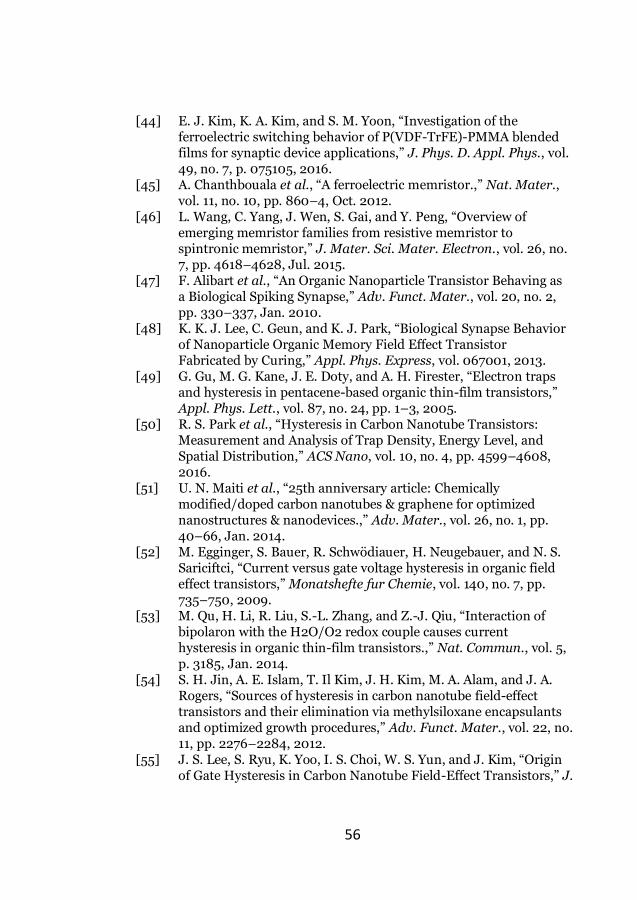
56
[44] E. J. Kim, K. A. Kim, and S. M. Yoon, “Investigation of the ferroelectric switching behavior of P(VDF-TrFE)-PMMA blended films for synaptic device applications,” J. Phys. D. Appl. Phys., vol. 49, no. 7, p. 075105, 2016.
[45] A. Chanthbouala et al., “A ferroelectric memristor.,” Nat. Mater., vol. 11, no. 10, pp. 860–4, Oct. 2012.
[46] L. Wang, C. Yang, J. Wen, S. Gai, and Y. Peng, “Overview of emerging memristor families from resistive memristor to spintronic memristor,” J. Mater. Sci. Mater. Electron., vol. 26, no. 7, pp. 4618–4628, Jul. 2015.
[47] F. Alibart et al., “An Organic Nanoparticle Transistor Behaving as a Biological Spiking Synapse,” Adv. Funct. Mater., vol. 20, no. 2, pp. 330–337, Jan. 2010.
[48] K. K. J. Lee, C. Geun, and K. J. Park, “Biological Synapse Behavior of Nanoparticle Organic Memory Field Effect Transistor Fabricated by Curing,” Appl. Phys. Express, vol. 067001, 2013.
[49] G. Gu, M. G. Kane, J. E. Doty, and A. H. Firester, “Electron traps and hysteresis in pentacene-based organic thin-film transistors,” Appl. Phys. Lett., vol. 87, no. 24, pp. 1–3, 2005.
[50] R. S. Park et al., “Hysteresis in Carbon Nanotube Transistors: Measurement and Analysis of Trap Density, Energy Level, and Spatial Distribution,” ACS Nano, vol. 10, no. 4, pp. 4599–4608, 2016.
[51] U. N. Maiti et al., “25th anniversary article: Chemically modified/doped carbon nanotubes & graphene for optimized nanostructures & nanodevices.,” Adv. Mater., vol. 26, no. 1, pp. 40–66, Jan. 2014.
[52] M. Egginger, S. Bauer, R. Schwödiauer, H. Neugebauer, and N. S. Sariciftci, “Current versus gate voltage hysteresis in organic field effect transistors,” Monatshefte fur Chemie, vol. 140, no. 7, pp. 735–750, 2009.
[53] M. Qu, H. Li, R. Liu, S.-L. Zhang, and Z.-J. Qiu, “Interaction of bipolaron with the H2O/O2 redox couple causes current hysteresis in organic thin-film transistors.,” Nat. Commun., vol. 5, p. 3185, Jan. 2014.
[54] S. H. Jin, A. E. Islam, T. Il Kim, J. H. Kim, M. A. Alam, and J. A. Rogers, “Sources of hysteresis in carbon nanotube field-effect transistors and their elimination via methylsiloxane encapsulants and optimized growth procedures,” Adv. Funct. Mater., vol. 22, no. 11, pp. 2276–2284, 2012.
[55] J. S. Lee, S. Ryu, K. Yoo, I. S. Choi, W. S. Yun, and J. Kim, “Origin of Gate Hysteresis in Carbon Nanotube Field-Effect Transistors,” J.
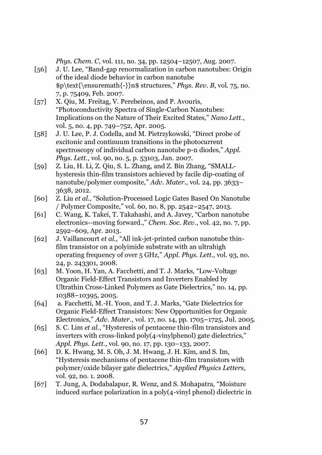
57
Phys. Chem. C, vol. 111, no. 34, pp. 12504–12507, Aug. 2007. [56] J. U. Lee, “Band-gap renormalization in carbon nanotubes: Origin
of the ideal diode behavior in carbon nanotube $p\text{\ensuremath{-}}n$ structures,” Phys. Rev. B, vol. 75, no. 7, p. 75409, Feb. 2007.
[57] X. Qiu, M. Freitag, V. Perebeinos, and P. Avouris, “Photoconductivity Spectra of Single-Carbon Nanotubes: Implications on the Nature of Their Excited States,” Nano Lett., vol. 5, no. 4, pp. 749–752, Apr. 2005.
[58] J. U. Lee, P. J. Codella, and M. Pietrzykowski, “Direct probe of excitonic and continuum transitions in the photocurrent spectroscopy of individual carbon nanotube p-n diodes,” Appl. Phys. Lett., vol. 90, no. 5, p. 53103, Jan. 2007.
[59] Z. Liu, H. Li, Z. Qiu, S. L. Zhang, and Z. Bin Zhang, “SMALL-hysteresis thin-film transistors achieved by facile dip-coating of nanotube/polymer composite,” Adv. Mater., vol. 24, pp. 3633–3638, 2012.
[60] Z. Liu et al., “Solution-Processed Logic Gates Based On Nanotube / Polymer Composite,” vol. 60, no. 8, pp. 2542–2547, 2013.
[61] C. Wang, K. Takei, T. Takahashi, and A. Javey, “Carbon nanotube electronics--moving forward.,” Chem. Soc. Rev., vol. 42, no. 7, pp. 2592–609, Apr. 2013.
[62] J. Vaillancourt et al., “All ink-jet-printed carbon nanotube thin-film transistor on a polyimide substrate with an ultrahigh operating frequency of over 5 GHz,” Appl. Phys. Lett., vol. 93, no. 24, p. 243301, 2008.
[63] M. Yoon, H. Yan, A. Facchetti, and T. J. Marks, “Low-Voltage Organic Field-Effect Transistors and Inverters Enabled by Ultrathin Cross-Linked Polymers as Gate Dielectrics,” no. 14, pp. 10388–10395, 2005.
[64] a. Facchetti, M.-H. Yoon, and T. J. Marks, “Gate Dielectrics for Organic Field-Effect Transistors: New Opportunities for Organic Electronics,” Adv. Mater., vol. 17, no. 14, pp. 1705–1725, Jul. 2005.
[65] S. C. Lim et al., “Hysteresis of pentacene thin-film transistors and inverters with cross-linked poly(4-vinylphenol) gate dielectrics,” Appl. Phys. Lett., vol. 90, no. 17, pp. 130–133, 2007.
[66] D. K. Hwang, M. S. Oh, J. M. Hwang, J. H. Kim, and S. Im, “Hysteresis mechanisms of pentacene thin-film transistors with polymer/oxide bilayer gate dielectrics,” Applied Physics Letters, vol. 92, no. 1. 2008.
[67] T. Jung, A. Dodabalapur, R. Wenz, and S. Mohapatra, “Moisture induced surface polarization in a poly(4-vinyl phenol) dielectric in
58
an organic thin-film transistor,” Appl. Phys. Lett., vol. 87, no. 18, p. 182109, Oct. 2005.
[68] S. P. Adhikari, M. P. Sah, H. Kim, L. O. Chua, and L. Fellow, “Three Fingerprints of Memristor,” vol. 60, no. 11, pp. 3008–3021, 2013.
[69] D. Abbott and F. Ieee, “Spike-Based Synaptic Plasticity in Silicon : Design , Implementation , Application , and Challenges,” Proc. IEEE, vol. 102, no. 5, 2014.
[70] G. Daoudal and D. Debanne, “Long-Term Plasticity of Intrinsic Excitability : Learning Rules and Mechanisms,” Learn. Mem., vol. 10, pp. 456–465, 2003.
[71] N. Zheng and I. M. Raman, “Synaptic inhibition, excitation, and plasticity in neurons of the cerebellar nuclei,” Cerebellum, vol. 9, no. 1. pp. 56–66, 2010.
[72] S. Friedmann, J. Schemmel, A. Grubl, A. Hartel, M. Hock, and K. Meier, “Demonstrating Hybrid Learning in a Flexible Neuromorphic Hardware System,” IEEE Trans. Biomed. Circuits Syst., vol. 11, no. 1, pp. 128–142, 2017.
[73] A. M. Shen, K. Kim, A. Tudor, D. Lee, and Y. Chen, “Doping modulated carbon nanotube synapstors for a spike neuromorphic module.,” Small, vol. 11, no. 13, pp. 1571–9, Apr. 2015.
[74] S. Marsland, Machine Learning, an Algorithmic Perspective, 2nd ed. CSC-Press, 2009.
[75] P. Maier et al., “Light sensitive memristor with bi-directional and wavelength-dependent conductance control,” Appl. Phys. Lett., vol. 109, no. 2, 2016.
[76] L. Deng, “The MNIST database of handwritten digit images for machine learning research,” IEEE Signal Process. Mag., vol. 29, no. 6, pp. 141–142, 2012.
[77] H. Sirringhaus, “Reliability of organic field-effect transistors,” Adv. Mater., vol. 21, no. 38–39, pp. 3859–3873, 2009.
[78] H. Sirringhaus, “25Th Anniversary Article: Organic Field-Effect Transistors: the Path Beyond Amorphous Silicon.,” Adv. Mater., vol. 26, no. 9, pp. 1319–35, Mar. 2014.