Embed Size (px)
Citation preview

April 2012
© 2012 Fairchild Semiconductor Corporation www.fairchildsemi.com FLS0116 • Rev. 1.0.0
FL
S0116 —
MO
SF
ET
Integ
rated S
mart L
ED
Lam
p D
river IC w
ith P
FC
Fu
nctio
n
FLS0116 MOSFET Integrated Smart LED Lamp Driver IC with PFC Function
Features
Built-in MOSFET(1A/550V)
Digitally Implemented Active-PFC Function
No Additional Circuit for Achieving High PF
Application Input Range: 80VAC ~ 308VAC
Built-In HV Supplying Circuit: Self Biasing
AOCP Function with Auto-Restart Mode
Built-In Over-Temperature Protection (OTP)
Cycle-by-Cycle Current Limit
Current Sense Pin Open Protection
Low Operating Current: 0.85mA (Typical)
Under-Voltage Lockout with 5V Hysteresis
Programmable Oscillation Frequency
Programmable LED Current
Analog Dimming Function
Soft-Start Function
Precise Internal Reference: ±3%
Applications
LED Lamp for Decorative Lighting
LED Lamp for Low-Power Lighting Fixture
Description
The FLS0116 LED lamp driver is a simple IC with integrated MOSFET and PFC function. The special “adopted digital” technique automatically detects input voltage condition and sends an internal reference signal to achieve high power factor. When AC input is applied to the IC, the PFC function is automatically enabled. When DC input is applied to the IC, the PFC function is automatically disabled. The FLS0116 does not need a bulk (electrolytic) capacitor for supply rail stability, which significantly improves LED lamp life.
Figure 1. Typical Application
Ordering Information
Part Number Operating
Temperature Range Package Packing Method
FLS0116MX -40°C to +125°C 7-Lead, Small-Outline Integrated Circuit (SOIC),
JEDEC MS-012, .150-inch, Narrow Body Tape & Reel
© 2012 Fairchild Semiconductor Corporation www.fairchildsemi.com FLS0116 • Rev. 1.0.0 2
FL
S0116 —
MO
SF
ET
Integ
rated S
mart L
ED
Lam
p D
river IC w
ith P
FC
Fu
nctio
n
Block Diagram
GND
RT
VCC HV
Reference
ADIM
JFET
AOCP
IAD
UVLO
QR
S
TSD
Leading-Edge Blanking
ZCD
DAC
Soft-Start
Digital Block
CS
Oscillator
-
+
LEB
-
+
time
VCC
ZCD
2.5V
FLS0116
DRAIN
7
8
1
3
4
5
2
Figure 2. Block Diagram
Pin Configuration
FL
S0116
Figure 3. Pin Configuration
Pin Definitions
Pin # Name Description
1 CS Current Sense. Limits output current, depending on the sensing resistor voltage. The CS pin is also used to set the LED current regulation.
2 VCC VCC. Supply pin for stable IC operation; ZCD signal detection used for accurate PFC function.
3 GND GROUND. Ground for the IC
4 RT RT. Programmable operating frequency using an external resistor; the IC has pre-fixed frequency when this pin is open or floating.
5 ADIM Analog Dimming. Connect to the internal current source. Use to change the output current using an external resistor. If ADIM is not used, connect a 0.1µF bypass capacitor between the ADIM and GND.
7 HV High Voltage. Connect to the high-voltage line and supply current to the IC.
8 DRAIN DRAIN. The drain pin of internal MOSFET
© 2012 Fairchild Semiconductor Corporation www.fairchildsemi.com FLS0116 • Rev. 1.0.0 3
FL
S0116 —
MO
SF
ET
Integ
rated S
mart L
ED
Lam
p D
river IC w
ith P
FC
Fu
nctio
n
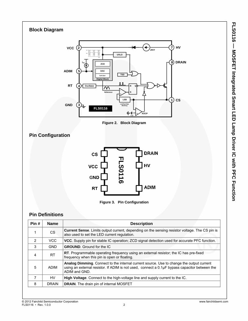
Absolute Maximum Ratings
Stresses exceeding the absolute maximum ratings may damage the device. The device may not function or be operable above the recommended operating conditions and stressing the parts to these levels is not recommended. In addition, extended exposure to stresses above the recommended operating conditions may affect device reliability. The absolute maximum ratings are stress ratings only.
Symbol Parameter Min. Max. Unit
VCC IC Supply Voltage 20 V
HV High Voltage Sensing 550 V
DRAIN Internal Drain Voltage 550 V
VADIM Analog Dimming 5 V
VRT RT Pin Voltage 5 V
VCS Allowable Current Sensing Detection Voltage 5 V
TA Operating Ambient Temperature Range -40 +125 °C
TJ Operating Junction Temperature -40 +150 °C
TSTG Storage Temperature Range -65 +150 °C
θJA Thermal Resistance Junction-Air(1,2) 135 °C/W
PD Power Dissipation 660 mW
ESD Electrostatic Discharge Capability Human Body Model, JESD22-A114 2000
V Charged Device Model, JESD22-C101 1000
Notes: 1. Thermal resistance test board. Size: 76.2mm x 114.3mm x 1.6mm (1S0P); JEDEC standard: JESD51-2, JESD51-3. 2. Assume no ambient airflow.

© 2012 Fairchild Semiconductor Corporation www.fairchildsemi.com FLS0116 • Rev. 1.0.0 4
FL
S0116 —
MO
SF
ET
Integ
rated S
mart L
ED
Lam
p D
river IC w
ith P
FC
Fu
nctio
n
Electrical Characteristics
Typical values are at TA = +25°C. Specifications to -40°C ~ 125°C are guaranteed by design based on final characterization results.
Symbol Parameter Condition Min. Typ. Max. Unit
VCC Bias Section
VCC VCC Regulator Output Voltage VHV=100VDC 14.0 15.5 17.0 V
VCCST+ UVLO Positive-Going Threshold VCC Increasing 12 13 14 V
VCCST- UVLO Negative-Going Threshold VCC Decreasing 7 8 9 V
VCCHYS UVLO Hysteresis 4 5 6 V
IHV HV Pin Current VHV=100VDC, RT=Open 0.85 1.2 mA
IST Startup Current 120 150 μA
Switching Section
fOSC Operating Frequency
RT=5.95kΩ 200 250 300 kHz
RT=87kΩ 16 20 24 kHz
RT Open 40.5 45.0 49.5 kHz
tMIN Minimum On Time(3) 400 ns
DMAX Maximum Duty Cycle 50 %
tLEB Leading Edge Blanking Time(3) 350 ns
VRT Voltage Reference of RT Pin 1.5 V
Soft-Start Section
tss Soft-Start Time(3) DC Mode 48 60 72 ms
AC Mode 7 Periods
Reference Section
VCS1 Internal Reference Voltage of CS Pin
DC Mode 0.354 0.365 0.376 V
VCS2 AC Mode(3) 0.485 0.500 0.515
Protection Section
OVPVCC Over-Voltage Protection on VCC Pin 17.7 18.7 19.7 V
VAOCP Abnormal OCP Level at CS Pin(3) 2.5 V
tAOCP Abnormal Detection Time(3) 70 ns
TTSDH Thermal Shutdown Threshold(3) 140 150 °C
TTSDHY Thermal Shutdown Threshold Hysteresis(3)
50 °C
Dimming Section
VADIM(ST+) Analog Dimming Positive Going Threshold(3)
3.15 3.50 3.85 V
VADIM(ST-) Analog Dimming Negative Going Threshold(3)
0.50 0.75 V
IAD Internal Current Source for ADIM Pin 9 12 15 μA
Continued on the following page…
© 2012 Fairchild Semiconductor Corporation www.fairchildsemi.com FLS0116 • Rev. 1.0.0 5
FL
S0116 —
MO
SF
ET
Integ
rated S
mart L
ED
Lam
p D
river IC w
ith P
FC
Fu
nctio
n
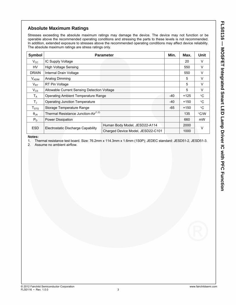
Electrical Characteristics (Continued)
Typical values are at TA = +25°C. Specifications to -40°C ~ 125°C are guaranteed by design based on final characterization results.
Symbol Parameter Condition Min. Typ. Max. Unit
MOSFET Section
BVDSS Breakdown Voltage VCC=0V, ID=250μA 550 V
ILKMOS Internal MOSFET Leakage Current VDS=550VDC, VGS=0V 250 μA
RON(ON) Drain-Source On Resistance(3) VGS=10V, VDGS=0V, TC=25°C
7.3 10.0 Ω
CISS Input Capacitance(3) VGS=0V,VDS=25V, f=1MHz 135 pF
COSS Output Capacitance(3) VGS=0V,VDS=25V, f=1MHz 21 pF
CRSS Reverse Transfer Capacitance(3) VGS=0V,VDS=25V, f=1MHz 3.2 pF
td(ON) Turn-On Delay(3) VDD=350V, ID=1A 10 ns
tr Rise Time(3) VDD=350V, ID=1A 13.4 ns
td(OFF) Turn-Off Delay(3) VDD=350V, ID=1A 14.9 ns
tf Fall Time(3) VDD=350V, ID=1A 36.8 ns
Note: 3. These parameters, although guaranteed, are not 100% tested in production.
© 2012 Fairchild Semiconductor Corporation www.fairchildsemi.com FLS0116 • Rev. 1.0.0 6
FL
S0116 —
MO
SF
ET
Integ
rated S
mart L
ED
Lam
p D
river IC w
ith P
FC
Fu
nctio
n
Functional Description
The FLS0116 is a basic PWM controller for buck converter topology in Continuous Conduction Mode (CCM) with an intelligent PFC function that uses a digital control algorithm. An internal self-biasing circuit uses the high-voltage switching device. The IC does not need an auxiliary powering path to the VCC pin typical in flyback control ICs or PSR product family.
When the input voltage applied to the HV pin is within operating range (25V to 500V), the FLS0116 maintains a 15.5V DC voltage at the VCC pin for stable operation. The UVLO block functions such that when the VCC voltage rises higher than VCCST+, the internal UVLO block releases and starts operation. Otherwise, the VCC goes down to the VCCST- and IC operation stops. Normally, the hysteresis function provides stable operation even if the input voltage is operating under very noisy or unstable circumstances.
The FLS0116 has a “smart” internal digital block for determining input condition: AC or DC. When an AC source with 50Hz or 60Hz is applied to the IC, the IC automatically changes its internal reference signal, which is similar to input signal, for creating high power factor. When a DC source connects to the IC, the internal reference immediately changes to DC.
Soft-Start Function The FLS0116 has an internal soft-start function to reduce inrush current at startup. When the IC starts operation following an internal sequence, the internal reference slowly increases for a pre-determined fixed time. After this transient period, the internal reference goes to a steady-state level. In this time, the IC continually tries to find phase information from the VCC pin. If the IC succeeds in getting phase information, it automatically follows a similar shape reference made during the transient times, 7 periods. If not, the IC has a DC reference level.
Figure 4. Soft-Start Function in AC Input Mode
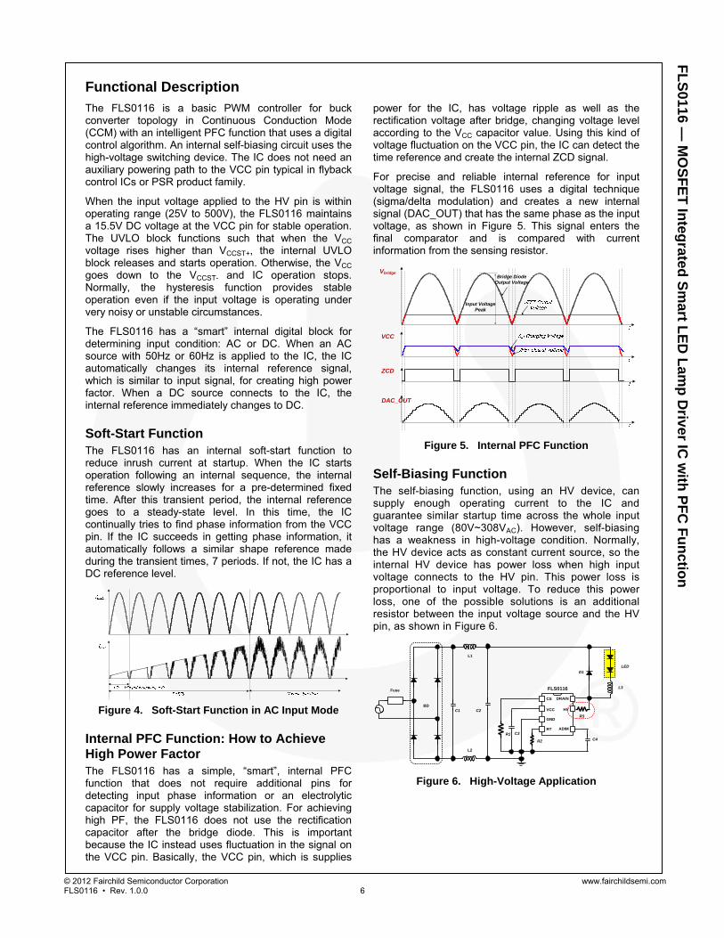
Internal PFC Function: How to Achieve High Power Factor The FLS0116 has a simple, “smart”, internal PFC function that does not require additional pins for detecting input phase information or an electrolytic capacitor for supply voltage stabilization. For achieving high PF, the FLS0116 does not use the rectification capacitor after the bridge diode. This is important because the IC instead uses fluctuation in the signal on the VCC pin. Basically, the VCC pin, which is supplies
power for the IC, has voltage ripple as well as the rectification voltage after bridge, changing voltage level according to the VCC capacitor value. Using this kind of voltage fluctuation on the VCC pin, the IC can detect the time reference and create the internal ZCD signal.
For precise and reliable internal reference for input voltage signal, the FLS0116 uses a digital technique (sigma/delta modulation) and creates a new internal signal (DAC_OUT) that has the same phase as the input voltage, as shown in Figure 5. This signal enters the final comparator and is compared with current information from the sensing resistor.
DAC_OUT
Bridge DiodeOutput Voltage
Input Voltage Peak
ZCD
VCC
Vbridge
Figure 5. Internal PFC Function
Self-Biasing Function The self-biasing function, using an HV device, can supply enough operating current to the IC and guarantee similar startup time across the whole input voltage range (80V~308VAC). However, self-biasing has a weakness in high-voltage condition. Normally, the HV device acts as constant current source, so the internal HV device has power loss when high input voltage connects to the HV pin. This power loss is proportional to input voltage. To reduce this power loss, one of the possible solutions is an additional resistor between the input voltage source and the HV pin, as shown in Figure 6.
D1
Fuse
C1 C2
L2
R2
FLS0116
CS
VCC
GND
RT
DRAIN
HV
ADIM
L1
L3
C3 R1C4
BD
LED
R3
Figure 6. High-Voltage Application
© 2012 Fairchild Semiconductor Corporation www.fairchildsemi.com FLS0116 • Rev. 1.0.0 7
FL
S0116 —
MO
SF
ET
Integ
rated S
mart L
ED
Lam
p D
river IC w
ith P
FC
Fu
nctio
n
Dimming Function The FLS0116 uses the ADIM pin for analog or 0V to 10V dimming. The peak voltage of internal reference, which is DAC_OUT signal in Figure 5, is changed by the VADIM level, as shown in Figure 7, and has different peak level according to the operating mode.
Figure 7. VADIM vs. VDAC_OUT(peak)
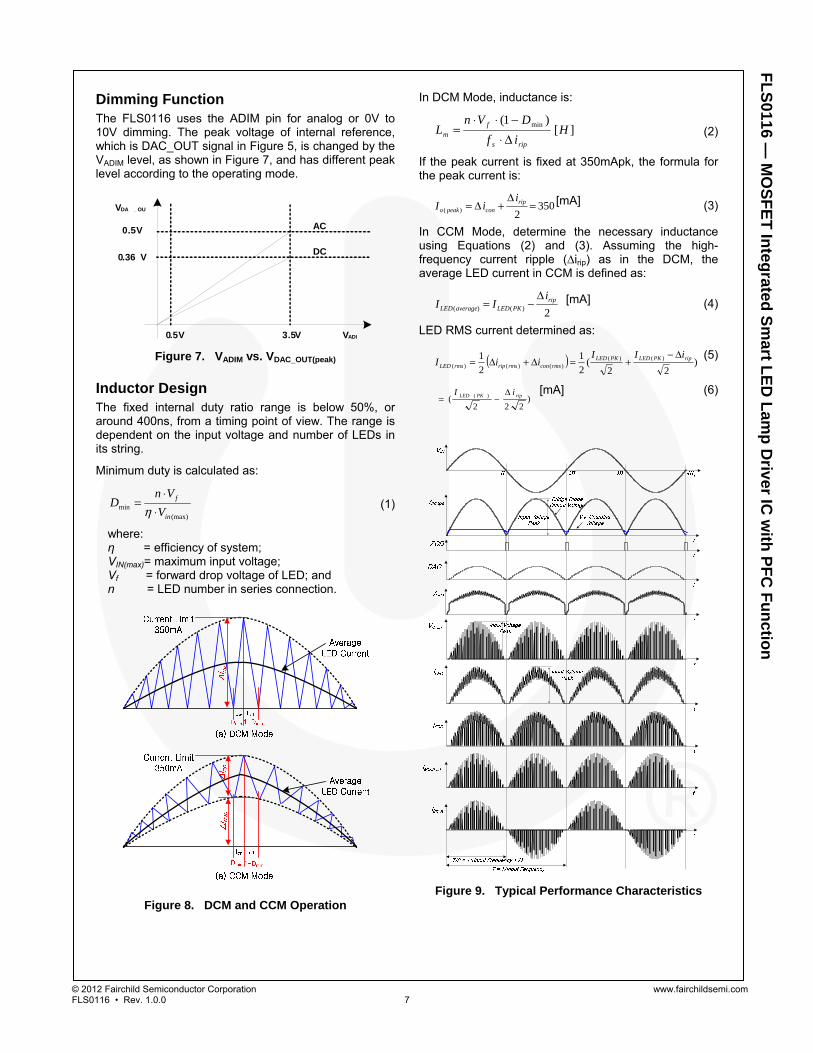
Inductor Design The fixed internal duty ratio range is below 50%, or around 400ns, from a timing point of view. The range is dependent on the input voltage and number of LEDs in its string.
Minimum duty is calculated as:
(max)min
in
f
VVn
D⋅
⋅=
η
(1)
where: η = efficiency of system; VIN(max)= maximum input voltage; Vf = forward drop voltage of LED; and n = LED number in series connection.
Figure 8. DCM and CCM Operation
In DCM Mode, inductance is:
][)1( min H
ifDVn
Lrips
fm Δ⋅
−⋅⋅= (2)
If the peak current is fixed at 350mApk, the formula for the peak current is:
3502)( =
Δ+Δ= rip
conpeako
iiI [mA] (3)
In CCM Mode, determine the necessary inductance using Equations (2) and (3). Assuming the high-frequency current ripple (∆irip) as in the DCM, the average LED current in CCM is defined as:
2)()(rip
PKLEDaverageLED
iII
Δ−= [mA] (4)
LED RMS current determined as:
( ) )22
(21
21 )()(
)()()(ripPKLEDPKLED
rmsconrmsriprmsLED
iIIiiI
Δ−+=Δ+Δ=
(5)
)222
( )( ripPKLED iI Δ−=
[mA] (6)
Figure 9. Typical Performance Characteristics
VADI
V DA _ OU
AC
DC
0.5V
0.36 V
3.5V0. 5V
© 2012 Fairchild Semiconductor Corporation www.fairchildsemi.com FLS0116 • Rev. 1.0.0 8
FL
S0116 —
MO
SF
ET
Integ
rated S
mart L
ED
Lam
p D
river IC w
ith P
FC
Fu
nctio
n
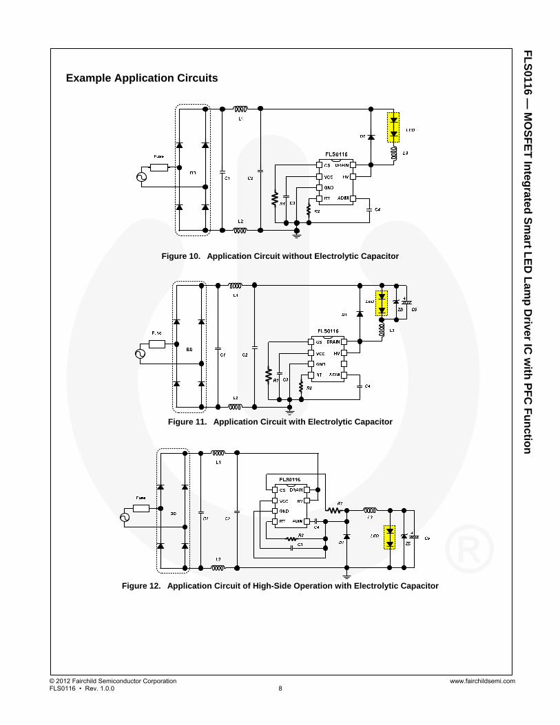
Example Application Circuits
Figure 10. Application Circuit without Electrolytic Capacitor
Figure 11. Application Circuit with Electrolytic Capacitor
Figure 12. Application Circuit of High-Side Operation with Electrolytic Capacitor
© 2011 Fairchild Semiconductor Corporation www.fairchildsemi.com FLS0116 • Rev. 1.0.0 9
FL
S0116 —
MO
SF
ET
Integ
rated S
mart L
ED
Lam
p D
river IC w
ith P
FC
Fu
nctio
n
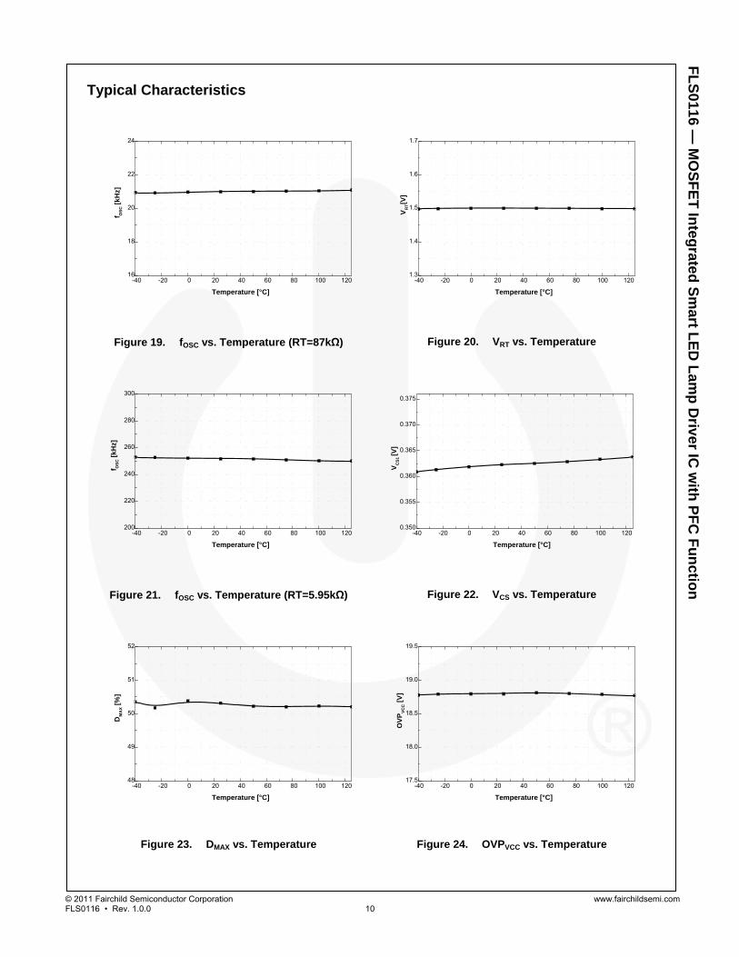
Typical Characteristics
-40 -20 0 20 40 60 80 100 12014.0
14.5
15.0
15.5
16.0
16.5
17.0
VC
C[V
]
Temperature [°C]
-40 -20 0 20 40 60 80 100 1204.0
4.5
5.0
5.5
6.0
VC
CH
V [
V]
Temperature [°C]
Figure 13. VCC vs. Temperature Figure 14. VCCHYS vs. Temperature
-40 -20 0 20 40 60 80 100 12012.0
12.5
13.0
13.5
14.0
VC
CS
T+[V
]
Temperature [°C]
-40 -20 0 20 40 60 80 100 12090
100
110
120
130
140
150I S
T[υ
A]
Temperature [°C]
Figure 15. VCCST+ vs. Temperature Figure 16. IST vs. Temperature
-40 -20 0 20 40 60 80 100 1207.0
7.5
8.0
8.5
9.0
VC
CS
T-[V
]
Temperature [°C]
-40 -20 0 20 40 60 80 100 12043
44
45
46
47
48
f OS
C [
kH
z]
Temperature [°C]
Figure 17. VCCST- vs. Temperature Figure 18. fOSC vs. Temperature (RT=Open)
© 2011 Fairchild Semiconductor Corporation www.fairchildsemi.com FLS0116 • Rev. 1.0.0 10
FL
S0116 —
MO
SF
ET
Integ
rated S
mart L
ED
Lam
p D
river IC w
ith P
FC
Fu
nctio
n
Typical Characteristics
-40 -20 0 20 40 60 80 100 12016
18
20
22
24
f OS
C [
kH
z]
Temperature [°C]
-40 -20 0 20 40 60 80 100 1201.3
1.4
1.5
1.6
1.7
VR
T[V
]
Temperature [°C]
Figure 19. fOSC vs. Temperature (RT=87kΩ) Figure 20. VRT vs. Temperature
-40 -20 0 20 40 60 80 100 120200
220
240
260
280
300
f OS
C [
kH
z]
Temperature [°C]
-40 -20 0 20 40 60 80 100 1200.350
0.355
0.360
0.365
0.370
0.375V
CS
1 [V
]
Temperature [°C]
Figure 21. fOSC vs. Temperature (RT=5.95kΩ) Figure 22. VCS vs. Temperature
-40 -20 0 20 40 60 80 100 12048
49
50
51
52
DM
AX [
%]
Temperature [°C]
-40 -20 0 20 40 60 80 100 12017.5
18.0
18.5
19.0
19.5
OV
PV
CC [
V]
Temperature [°C]
Figure 23. DMAX vs. Temperature Figure 24. OVPVCC vs. Temperature
© 2011 Fairchild Semiconductor Corporation www.fairchildsemi.com FLS0116 • Rev. 1.0.0 11
FL
S0116 —
MO
SF
ET
Integ
rated S
mart L
ED
Lam
p D
river IC w
ith P
FC
Fu
nctio
n
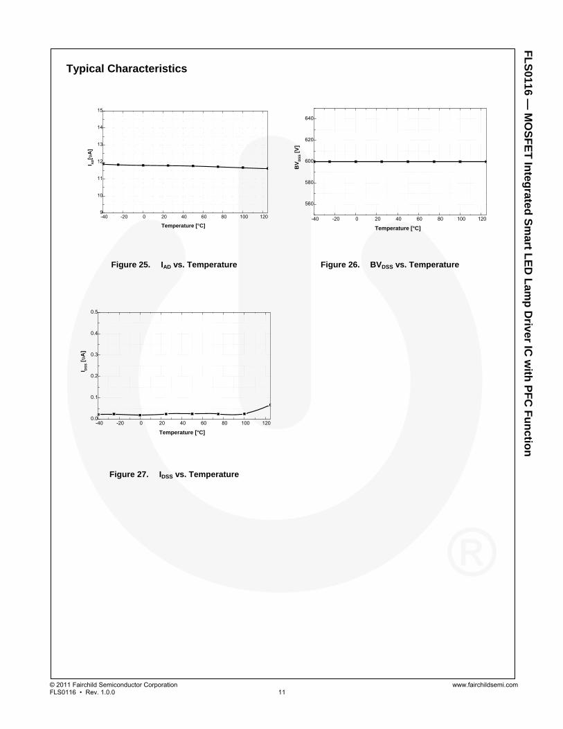
Typical Characteristics
-40 -20 0 20 40 60 80 100 1209
10
11
12
13
14
15
I AD[υ
A]
Temperature [°C]-40 -20 0 20 40 60 80 100 120
560
580
600
620
640
BV
DS
S [
V]
Temperature [°C]
Figure 25. IAD vs. Temperature Figure 26. BVDSS vs. Temperature
-40 -20 0 20 40 60 80 100 1200.0
0.1
0.2
0.3
0.4
0.5
I DS
S [
υA]
Temperature [°C]
Figure 27. IDSS vs. Temperature
© 2011 Fairchild Semiconductor Corporation www.fairchildsemi.com FLS0116 • Rev. 1.0.0 12
FL
S0116 —
MO
SF
ET
Integ
rated S
mart L
ED
Lam
p D
river IC w
ith P
FC
Fu
nctio
n
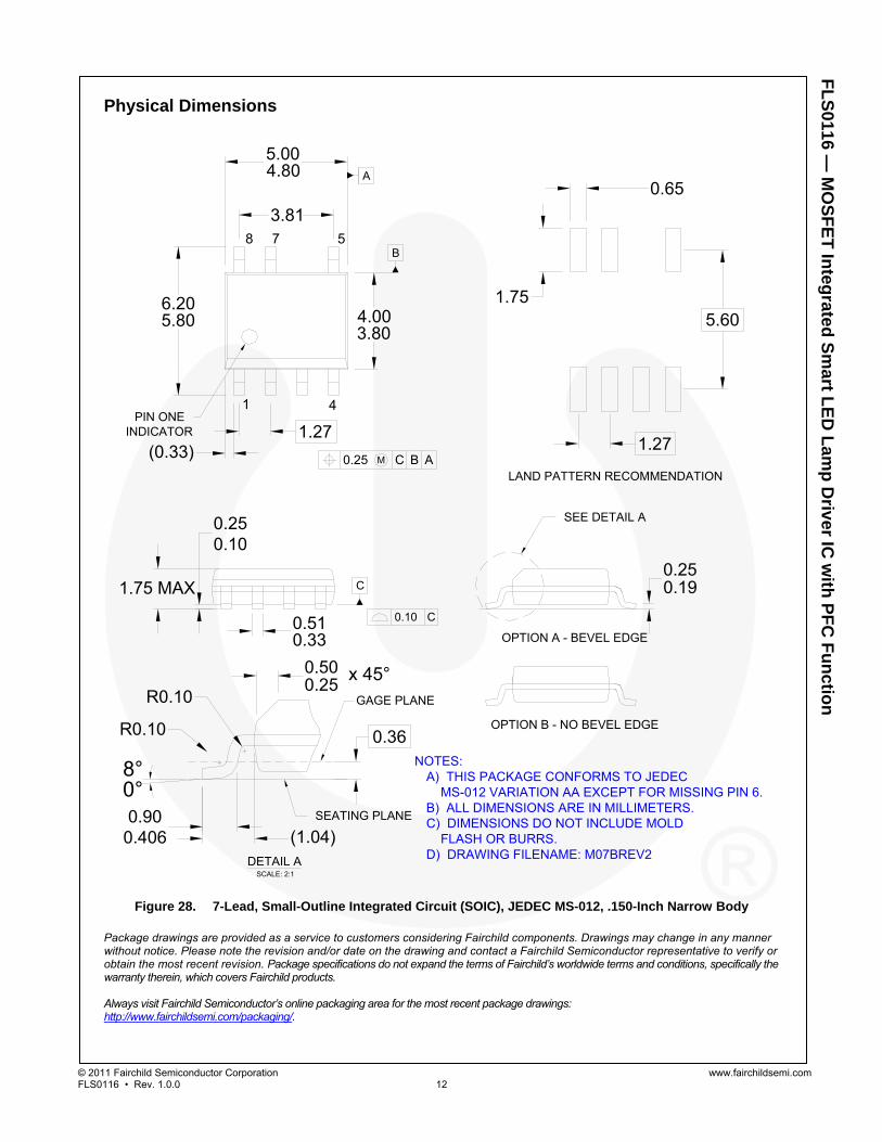
Physical Dimensions
8°0°
SEE DETAIL A
NOTES: A) THIS PACKAGE CONFORMS TO JEDEC MS-012 VARIATION AA EXCEPT FOR MISSING PIN 6. B) ALL DIMENSIONS ARE IN MILLIMETERS. C) DIMENSIONS DO NOT INCLUDE MOLD FLASH OR BURRS. D) DRAWING FILENAME: M07BREV2
LAND PATTERN RECOMMENDATION
SEATING PLANE
0.10 C
C
GAGE PLANE
x 45°
DETAIL ASCALE: 2:1
PIN ONEINDICATOR
4
8
1
CM B A0.25
B5
A
5.60
0.65
1.75
1.27
6.205.80
3.81
4.003.80
5.004.80
(0.33)1.27
0.510.33
0.250.10
1.75 MAX0.250.19
0.36
0.500.25
R0.10
R0.10
0.900.406 (1.04)
OPTION A - BEVEL EDGE
OPTION B - NO BEVEL EDGE
7
Figure 28. 7-Lead, Small-Outline Integrated Circuit (SOIC), JEDEC MS-012, .150-Inch Narrow Body
Package drawings are provided as a service to customers considering Fairchild components. Drawings may change in any manner without notice. Please note the revision and/or date on the drawing and contact a Fairchild Semiconductor representative to verify or obtain the most recent revision. Package specifications do not expand the terms of Fairchild’s worldwide terms and conditions, specifically the warranty therein, which covers Fairchild products. Always visit Fairchild Semiconductor’s online packaging area for the most recent package drawings: http://www.fairchildsemi.com/packaging/.

© 2011 Fairchild Semiconductor Corporation www.fairchildsemi.com FLS0116 • Rev. 1.0.0 13
FL
S0116 —
MO
SF
ET
Integ
rated S
mart L
ED
Lam
p D
river IC w
ith P
FC
Fu
nctio
n