Embed Size (px)
Citation preview
June 1996
Flyback Transformer Design ForTOPSwitch® Power SuppliesApplication Note AN-17
total flyback component cost is lower when compared to othertechniques. Between 75 and 100 Watts, increasing voltage andcurrent stresses cause flyback component cost to increasesignificantly. At higher power levels, topologies with lowervoltage and current stress levels (such as the forward converter)may be more cost effective even with higher component counts.
Flyback transformer design, which requires iteration through aset of design equations, is not difficult. Simple spreadsheetiteration reduces design time to under 10 minutes for a transformer
When developing TOPSwitch flyback power supplies,transformer design is usually the biggest stumbling block.Flyback transformers are not designed or used like normaltransformers. Energy is stored in the core. The core must begapped. Current effectively flows in either the primary orsecondary winding but never in both windings at the sametime.
Why use the flyback topology? Flyback power supplies use theleast number of components. At power levels below 75 watts,
®
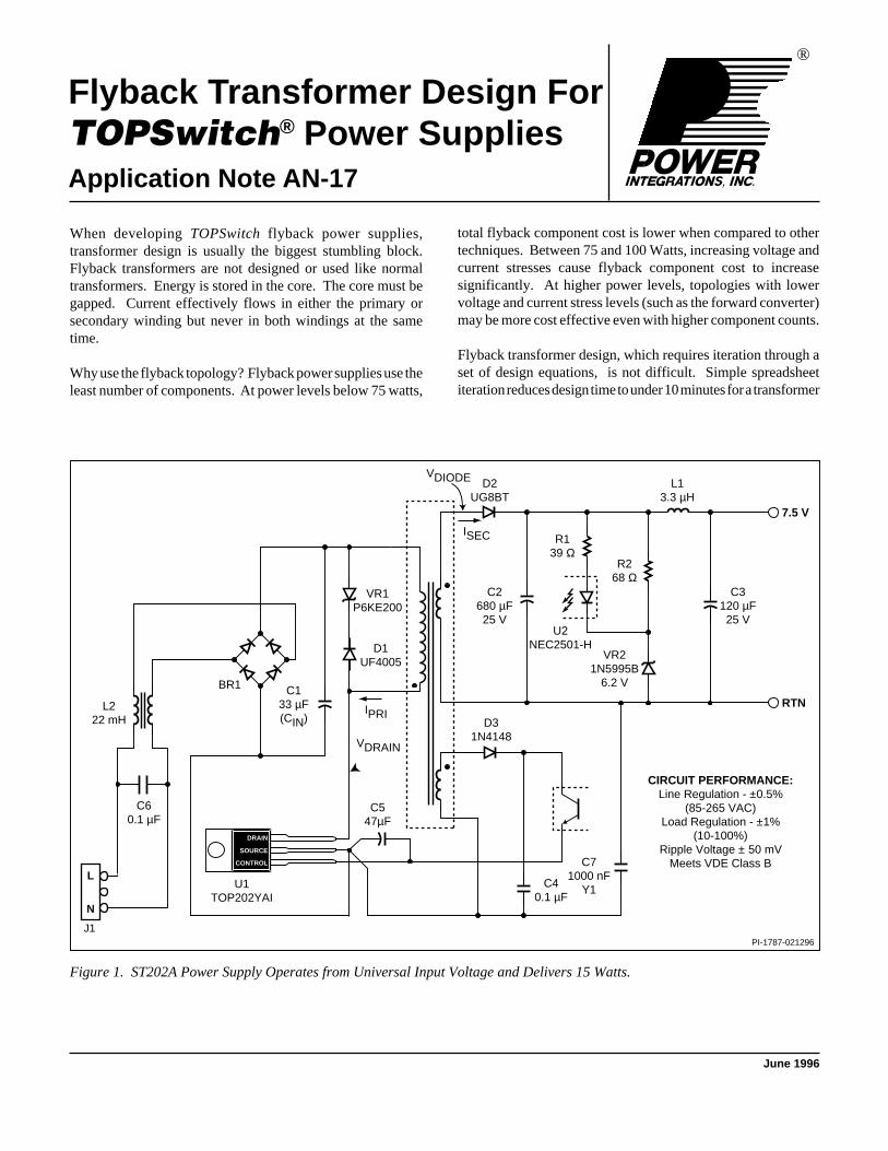
Figure 1. ST202A Power Supply Operates from Universal Input Voltage and Delivers 15 Watts.
PI-1787-021296
7.5 V
RTN
C547µF
D2UG8BT
D31N4148
R268 Ω
VR21N5995B
6.2 V
C3120 µF25 V
D1UF4005
C2680 µF25 V
VR1P6KE200
CIRCUIT PERFORMANCE:Line Regulation - ±0.5%
(85-265 VAC)Load Regulation - ±1%
(10-100%)Ripple Voltage ± 50 mV
Meets VDE Class B
BR1 C133 µF(CIN)
R139 Ω
U2NEC2501-H
U1TOP202YAI
DRAIN
SOURCE
CONTROL
C40.1 µF
C71000 nF
Y1
L13.3 µH
J1
C60.1 µF
L222 mH
L
N
IPRI
ISEC
VDIODE
VDRAIN
AN-17
C6/962
that usually works the first time. This method, used forcontinuous mode as well as discontinuous mode designs, hasthree distinct steps:
1) Identify and estimate a set of independent variables(input) depending on application details, transformercore, and selected TOPSwitch.
2) Identify and calculate a set of dependent parameters(output).
3) Iterate specified independent variables until selecteddependent parameters fall within defined limits for apractical flyback transformer.
A simple PC spreadsheet (available from Power Integrationsfor Excel or compatible spreadsheet programs) automates thetransformer design method presented in this application note.(Note: this improved version has been completely revised andmay give slightly different answers compared to earlier versions.Refer to the last page of this application note for a completedescription of the changes.)
A new parameter, the ratio of primary ripple current to peakcurrent (K
RP), is introduced to describe the TOPSwitch drain
current waveform shape and simplify subsequent calculationssuch as RMS current and AC flux density.
Application specific independent variables include minimumand maximum AC input voltage, line frequency, TOPSwitchswitching frequency, output and bias voltages, output power,bridge rectifier conduction time, size of input energy storagecapacitor, power supply efficiency and power loss allocationbetween primary and secondary circuitry. Variables dependingon the transformer core and construction include effective corecross sectional area and magnetic path length, ungappedeffective inductance, bobbin physical winding width, marginwidth (for creepage distance and safety isolation), number ofprimary layers, and number of secondary turns. Variablesdepending on TOPSwitch include switching frequency, reflectedoutput voltage, ripple to peak current ratio, and TOPSwitchvoltage drop.
For a given application and transformer core, 20 of these 23independent variables will be calculated or estimated once andthen remain fixed during iteration. Only three variables,number of secondary turns N
S, ripple to peak current ratio K
RP,
and number of primary winding layers L will be changed duringthe iteration process.
Dependent parameters are divided into four groups: DC inputvoltage, primary current waveform shape, transformer design,and voltage stress. DC input voltage parameters are simply theminimum and maximum DC input voltage after the AC mainshave been rectified and filtered. Primary current waveform
shape parameters include maximum duty cycle, average current,peak current, ripple current, and RMS current to completelydefine transformer primary current and determine operation ineither continuous or discontinuous mode. Transformer designparameters include primary inductance, number of primaryturns, number of bias winding turns, gapped effective inductance,maximum flux density, AC flux density, ungapped core relativepermeability, estimated gap length, effective bobbin width,insulated primary wire diameter, insulation thickness, bareconductor cross section, primary current capacity, and secondarydesign parameters. Voltage stress parameters determine themaximum TOPSwitch off-state drain voltage and output rectifierpeak inverse voltage.
Of all these dependent parameters, only three require examinationand comparison within limits during iteration. Maximum fluxdensity B
M, gap length L
G, and primary current capacity CMA
are checked with each iteration until all three parameters arewithin specified limits. The remaining dependent parametersare either intermediate calculations or parameters used by themanufacturer for construction or the designer for specifyingcomponents.
Understanding primary and secondary current waveform shapein both continuous and discontinuous mode operation isnecessary before beginning transformer design.
Figure 1 shows a typical flyback power supply using theTOP202 TOPSwitch from Power Integrations, Inc. TOPSwitchcombines an integrated high voltage MOSFET switch with acomplete switching power supply controller and protectioncircuitry in a single 3 pin TO220 package. The TOPSwitchpower supply operates from 85 to 265 VAC and delivers 15Watts at 7.5 Volt output. AC power is rectified and filtered byBR1 and C1 (C
IN) to create the high voltage DC bus applied to
the primary winding of T1. The other side of the transformerprimary is driven by TOPSwitch. D1 and VR1 clamp voltagespikes caused by transformer leakage inductance. D2, C2, L1,and C3 rectify and filter the power secondary. TOPSwitch biasvoltage is provided by D3 and C4 which rectify and filter thebias winding. EMI filter components L2, C6, and C7 reduceconducted emission currents. Bypass capacitor C5 filtersinternal TOPSwitch gate charge current spikes and alsocompensates the control loop. Regulation is achieved when theoutput voltage rises sufficiently above Zener diode voltage(VR2) to cause optocoupler photodiode current to flow.Optocoupler phototransistor current flows into the TOPSwitchcontrol pin to directly control the duty cycle and output voltage.R1 together with series impedances of VR2 and TOPSwitchdetermine the control loop DC gain. R2 and VR2 provide aslight preload to improve regulation at light loads.
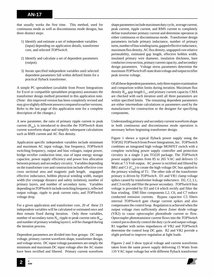
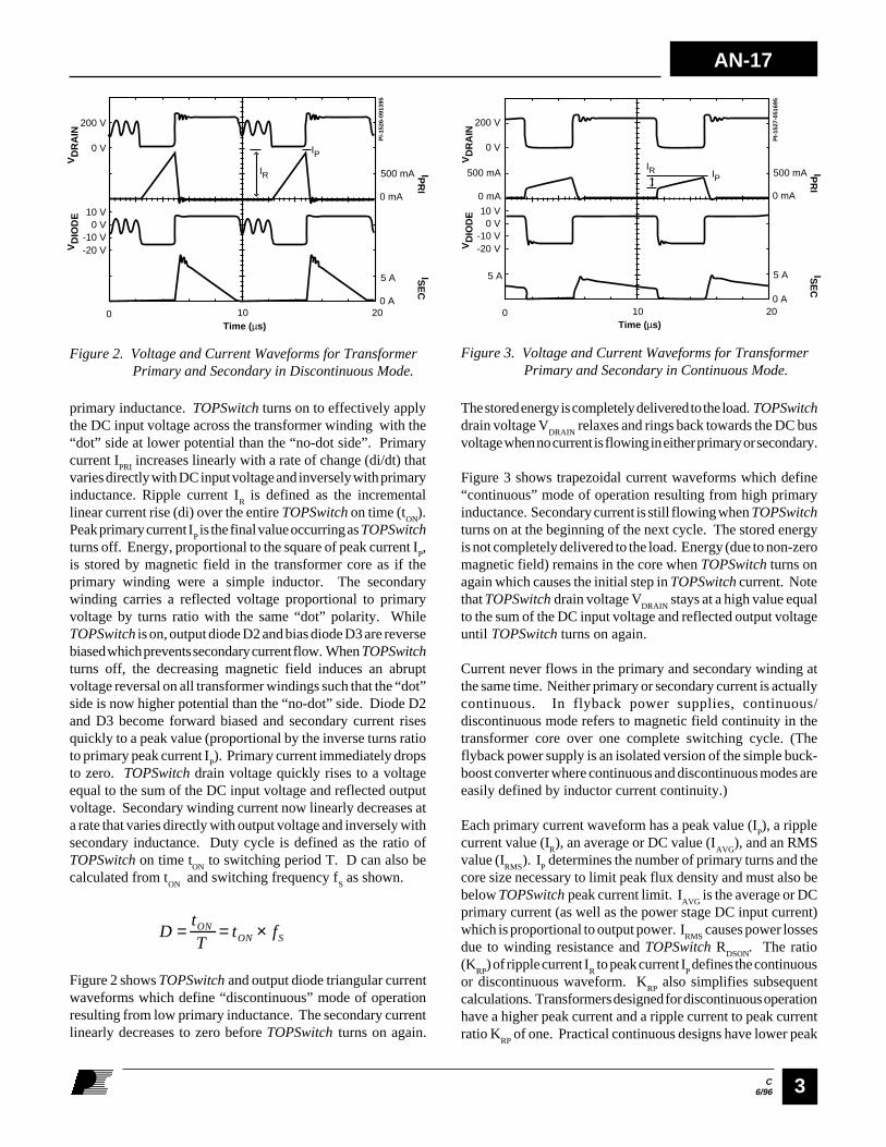
Figures 2 and 3 show typical voltage and current waveformstaken from the same power supply delivering 15 Watts from110 VAC input voltage but with different flyback transformer
C6/96
AN-17
3
PI-
1526
-091
395
0 10 20
-20 V-10 V
10 V
0 V
200 V
0 V
VD
RA
IN
0 mA
500 mA IPR
I
0 A
5 A ISE
C
VD
IOD
E
Time (µs)
IR
IP
PI-
1527
-051
695
0 10 20
Time (µs)
-20 V-10 V
10 V
0 V
200 V
0 V
VD
RA
IN
0 mA
500 mA IPR
I
0 A
5 A
IR IP
ISE
C
VD
IOD
E
5 A
500 mA
0 mA
Figure 3. Voltage and Current Waveforms for Transformer Primary and Secondary in Continuous Mode.
Figure 2. Voltage and Current Waveforms for Transformer Primary and Secondary in Discontinuous Mode.
primary inductance. TOPSwitch turns on to effectively applythe DC input voltage across the transformer winding with the“dot” side at lower potential than the “no-dot side”. Primarycurrent I
PRI increases linearly with a rate of change (di/dt) that
varies directly with DC input voltage and inversely with primaryinductance. Ripple current I
R is defined as the incremental
linear current rise (di) over the entire TOPSwitch on time (tON
).Peak primary current I
P is the final value occurring as TOPSwitch
turns off. Energy, proportional to the square of peak current IP,
is stored by magnetic field in the transformer core as if theprimary winding were a simple inductor. The secondarywinding carries a reflected voltage proportional to primaryvoltage by turns ratio with the same “dot” polarity. WhileTOPSwitch is on, output diode D2 and bias diode D3 are reversebiased which prevents secondary current flow. When TOPSwitchturns off, the decreasing magnetic field induces an abruptvoltage reversal on all transformer windings such that the “dot”side is now higher potential than the “no-dot” side. Diode D2and D3 become forward biased and secondary current risesquickly to a peak value (proportional by the inverse turns ratioto primary peak current I
P). Primary current immediately drops
to zero. TOPSwitch drain voltage quickly rises to a voltageequal to the sum of the DC input voltage and reflected outputvoltage. Secondary winding current now linearly decreases ata rate that varies directly with output voltage and inversely withsecondary inductance. Duty cycle is defined as the ratio ofTOPSwitch on time t
ON to switching period T. D can also be
calculated from tON
and switching frequency fS as shown.
DtT
t fONON S= = ×
Figure 2 shows TOPSwitch and output diode triangular currentwaveforms which define “discontinuous” mode of operationresulting from low primary inductance. The secondary currentlinearly decreases to zero before TOPSwitch turns on again.
The stored energy is completely delivered to the load. TOPSwitchdrain voltage V
DRAIN relaxes and rings back towards the DC bus
voltage when no current is flowing in either primary or secondary.
Figure 3 shows trapezoidal current waveforms which define“continuous” mode of operation resulting from high primaryinductance. Secondary current is still flowing when TOPSwitchturns on at the beginning of the next cycle. The stored energyis not completely delivered to the load. Energy (due to non-zeromagnetic field) remains in the core when TOPSwitch turns onagain which causes the initial step in TOPSwitch current. Notethat TOPSwitch drain voltage V
DRAIN stays at a high value equal
to the sum of the DC input voltage and reflected output voltageuntil TOPSwitch turns on again.
Current never flows in the primary and secondary winding atthe same time. Neither primary or secondary current is actuallycontinuous. In flyback power supplies, continuous/discontinuous mode refers to magnetic field continuity in thetransformer core over one complete switching cycle. (Theflyback power supply is an isolated version of the simple buck-boost converter where continuous and discontinuous modes areeasily defined by inductor current continuity.)
Each primary current waveform has a peak value (IP), a ripple
current value (IR), an average or DC value (I
AVG), and an RMS
value (IRMS
). IP determines the number of primary turns and the
core size necessary to limit peak flux density and must also bebelow TOPSwitch peak current limit. I
AVG is the average or DC
primary current (as well as the power stage DC input current)which is proportional to output power. I
RMS causes power losses
due to winding resistance and TOPSwitch RDSON
. The ratio(K
RP) of ripple current I
R to peak current I
P defines the continuous
or discontinuous waveform. KRP
also simplifies subsequentcalculations. Transformers designed for discontinuous operationhave a higher peak current and a ripple current to peak currentratio K
RP of one. Practical continuous designs have lower peak
AN-17
C6/964
currents and a ripple to peak current ratio KRP
of less than onebut typically greater than 0.4. K
RP is inversely proportional to
primary inductance so a continuous design with lower KRP
willhave a higher inductance. Continuous transformer designshave a practical primary inductance upper limit approximatelyfour times that of a discontinuous design at the same inputvoltage and output power due to the difference in peak currentsand value of K
RP.
The primary current waveforms shown in Figures 2 and 3deliver the same output power and therefore (assuming equalefficiency) must have equal I
AVG. The discontinuous current
waveform has a higher peak value and therefore must have ahigher RMS current value. Discontinuous mode requires lessinductance and reduces transformer size but operates withhigher losses and lower efficiency due to higher RMS currents.Continuous mode requires higher inductance and largertransformer size but offers improved efficiency and lowerpower losses. The trade-off between transformer size andpower supply efficiency depends on the packaging and thermalenvironment in each application.
Some control loop comments regarding continuous mode are inorder here. Most designers tend to avoid the continuous modewhenever possible because the feedback control loop is moredifficult to analyze. Discontinuous mode power supplies aremodeled with a single pole response and are simple to stabilize.Continuous mode offers improved efficiency, reduced losses,lower component temperatures, or higher output power butanalysis is more difficult because a right half plane zero andcomplex pole pair all shift with duty cycle. However, stabilizinga continuous mode TOPSwitch power supply is quitestraightforward. Adequate phase margins are achievable overall line and load combinations because the 70% maximumTOPSwitch duty cycle DC
MAX (from the data sheet) limits right
half plane zero and complex pole pair migration. Phase marginis generally higher than expected once the damping effect ofeffective series power path resistance and output capacitor ESRis taken into account. Crossover bandwidths of 1 KHz (orwider) are easily achievable with phase margins of at least 45degrees. Refer to AN-14 for circuit techniques to use incontinuous mode designs.
Transformer core, winding, and safety issues must also bediscussed before beginning design.
Transformer core and construction parameters depend on theselected core and winding techniques used in assembly. Physicalheight and cost are usually most important when selectingcores. This is especially true in AC mains adapter powersupplies normally packaged in sealed plastic boxes. Applicationsallowing at least 0.75 inches of component height can use lowcost EE or EI cores from Magnetics, Inc., Japanese vendorsTDK and Tokin, or European vendors Philips, Siemens, and
Thomson. Applications requiring lower profile can benefitfrom EFD cores available from the European vendors. EERcores offer a large window area, require few turns, and havebobbins available with high pin counts for those applicationsrequiring multiple outputs. ETD cores are useful in the higherpower designs when space is not a problem. PQ cores are moreexpensive but take up slightly less PC board space and requireless turns than E cores. Safety isolation requirements make potcores, RM cores, and toroids generally not suitable for flybackpower supplies operating from the AC mains.
Flyback transformers must provide isolation between primaryand secondary in accordance with the regulatory agencies ofthe intended market. For example, information technologyequipment must meet the requirements of IEC950 in Europeand UL1950 in the U.S. These documents specify creepageand clearance distances as well as insulation systems used intransformer construction. 5 to 6 mm creepage distance isusually sufficient between primary and secondary (check withthe appropriate agency and specification). Isolation is usuallyspecified by electric strength and is tested with a voltage oftypically 3000 VAC applied for 60 seconds. Two layers ofinsulation (Basic and Supplementary) can be used betweenprimary and secondary if each layer exceeds the electricstrength requirement. Three layers of insulation (reinforced)can also be used if all combinations of two layers (out of totalthree layers) meets the electric strength requirement.
Figure 4a shows the margin winding technique used in mostflyback transformers. The margin is usually constructed withlayers of tape slit to the width of the desired margin andwrapped in sufficient layers to match the winding height. Themargin is generally half the required primary to secondarycreepage distance (2.5 mm in this example). Cores andbobbins should be selected large enough that the actual windingwidth is at least twice the total creepage distance to maintaintransformer coupling and reduce leakage inductance. Theprimary is wound between the margins. To reduce the risk ofinterlayer voltage breakdown due to insulation abrasion,improve layer to layer insulation, and decrease capacitance,the primary layers should be separated by at least one layer ofUL listed polyester film tape (3M 1298) cut to fit between themargins. Impregnation with varnish or epoxy can also improvethe layer to layer insulation and electric strength but does notreduce capacitance. The bias winding may then be wound overthe primary. Supplementary or reinforced insulation consistingof two or three layers of UL listed polyester film tape cut to thefull width of the bobbin may then be wrapped over the primaryand bias windings. Margins are again wound. The secondarywinding is wound between the margins. Another two or threelayers of tape is added to secure the windings. Insulationsleeving may be needed over the leads of one or all windingsto meet creepage distance requirements at lead exits. Nylon or
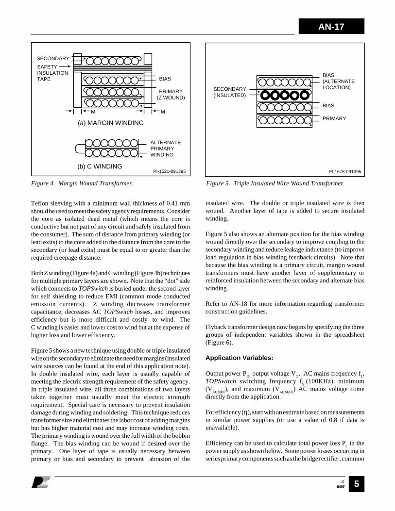
C6/96
AN-17
5
BIAS
BIAS (ALTERNATE LOCATION)
PRIMARY
PI-1678-091395
SECONDARY (INSULATED)
BIAS
MM
PRIMARY(Z WOUND)
ALTERNATEPRIMARYWINDING
SECONDARY
SAFETYINSULATIONTAPE
(a) MARGIN WINDING
(b) C WINDINGPI-1521-091395
Figure 5. Triple Insulated Wire Wound Transformer.Figure 4. Margin Wound Transformer.
Teflon sleeving with a minimum wall thickness of 0.41 mmshould be used to meet the safety agency requirements. Considerthe core as isolated dead metal (which means the core isconductive but not part of any circuit and safely insulated fromthe consumer). The sum of distance from primary winding (orlead exits) to the core added to the distance from the core to thesecondary (or lead exits) must be equal to or greater than therequired creepage distance.
Both Z winding (Figure 4a) and C winding (Figure 4b) techniquesfor multiple primary layers are shown. Note that the “dot” sidewhich connects to TOPSwitch is buried under the second layerfor self shielding to reduce EMI (common mode conductedemission currents). Z winding decreases transformercapacitance, decreases AC TOPSwitch losses, and improvesefficiency but is more difficult and costly to wind. TheC winding is easier and lower cost to wind but at the expense ofhigher loss and lower efficiency.
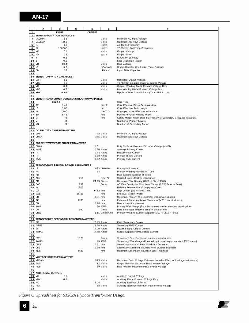
Figure 5 shows a new technique using double or triple insulatedwire on the secondary to eliminate the need for margins (insulatedwire sources can be found at the end of this application note).In double insulated wire, each layer is usually capable ofmeeting the electric strength requirement of the safety agency.In triple insulated wire, all three combinations of two layerstaken together must usually meet the electric strengthrequirement. Special care is necessary to prevent insulationdamage during winding and soldering. This technique reducestransformer size and eliminates the labor cost of adding marginsbut has higher material cost and may increase winding costs.The primary winding is wound over the full width of the bobbinflange. The bias winding can be wound if desired over theprimary. One layer of tape is usually necessary betweenprimary or bias and secondary to prevent abrasion of the
insulated wire. The double or triple insulated wire is thenwound. Another layer of tape is added to secure insulatedwinding.
Figure 5 also shows an alternate position for the bias windingwound directly over the secondary to improve coupling to thesecondary winding and reduce leakage inductance (to improveload regulation in bias winding feedback circuits). Note thatbecause the bias winding is a primary circuit, margin woundtransformers must have another layer of supplementary orreinforced insulation between the secondary and alternate biaswinding.
Refer to AN-18 for more information regarding transformerconstruction guidelines.
Flyback transformer design now begins by specifying the threegroups of independent variables shown in the spreadsheet(Figure 6).
Application Variables:
Output power PO, output voltage V
O, AC mains frequency f
L,
TOPSwitch switching frequency fS
(100KHz), minimum(V
ACMIN), and maximum (V
ACMAX) AC mains voltage come
directly from the application.
For efficiency (η), start with an estimate based on measurementsin similar power supplies (or use a value of 0.8 if data isunavailable).
Efficiency can be used to calculate total power loss PL in the
power supply as shown below. Some power losses occurring inseries primary components such as the bridge rectifier, common
AN-17
C6/966
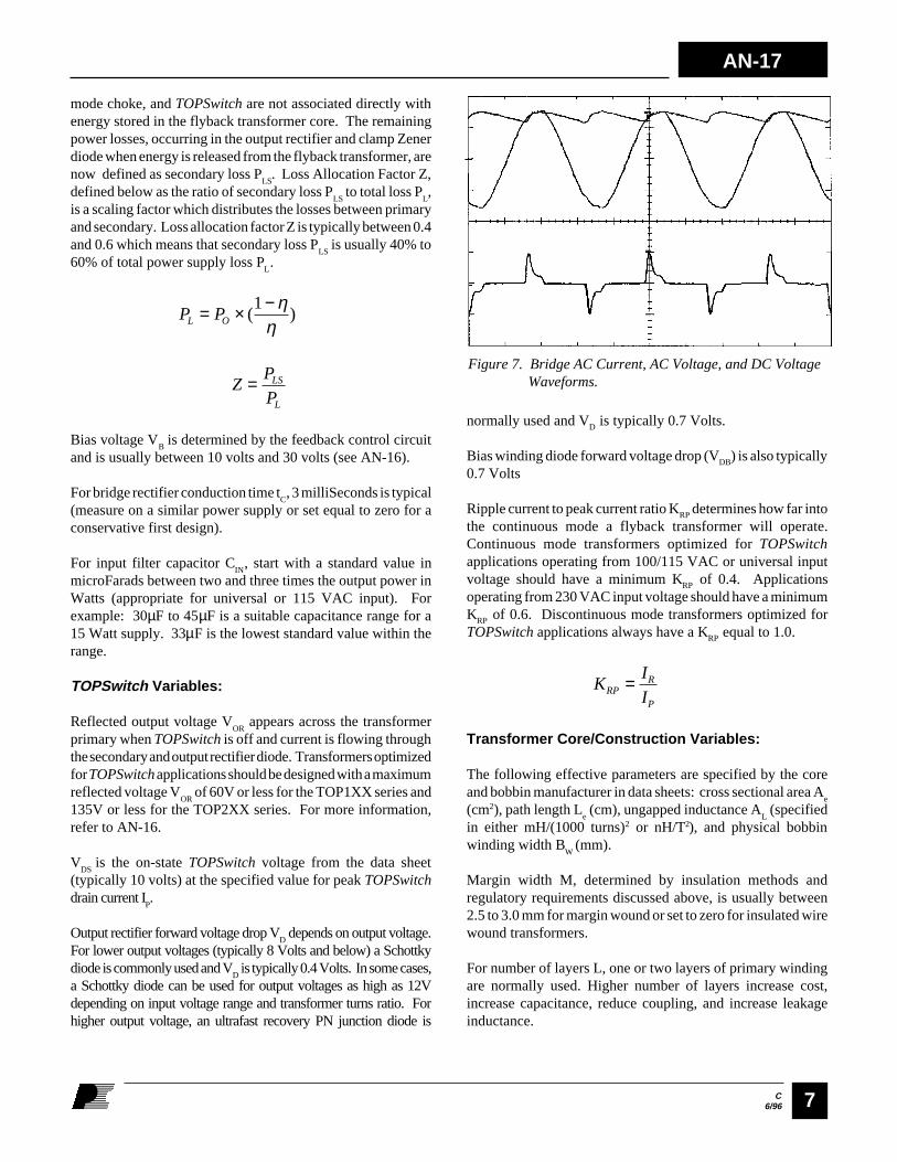
Figure 6. Spreadsheet for ST202A Flyback Transformer Design.
123456789
1 01 11 21 31 41 51 61 71 81 92 02 12 22 32 42 52 62 72 82 93 03 13 23 33 43 53 63 73 83 94 04 14 24 34 44 54 64 74 84 95 05 15 25 35 45 55 65 75 85 96 06 16 26 36 46 56 66 76 86 97 07 17 27 37 47 57 67 77 87 98 08 18 2
A B C D E F INPUT OUTPUTENTER APPLICATION VARIABLESVACMIN 8 5 Volts Minimum AC Input VoltageVACMAX 265 Volts Maximum AC Input VoltagefL 6 0 Hertz AC Mains FrequencyfS 100000 Hertz TOPSwitch Switching FrequencyVO 7.5 Volts Output VoltagePO 1 5 Watts Output Powern 0.8 Efficiency EstimateZ 0.5 Loss Allocation Factor VB 10.4 Volts Bias VoltagetC 3.2 mSeconds Bridge Rectifier Conduction Time EstimateCIN 3 3 uFarads Input Filter Capacitor
ENTER TOPSWITCH VARIABLESVOR 8 5 Volts Reflected Output VoltageVDS 1 0 Volts TOPSwitch on-state Drain to Source Voltage VD 0.4 Volts Output Winding Diode Forward Voltage DropVDB 0.7 Volts Bias Winding Diode Forward Voltage DropKRP 0.92 Ripple to Peak Current Ratio (0.4 < KRP < 1.0)
ENTER TRANSFORMER CORE/CONSTRUCTION VARIABLESEE22-Z Core Type
AE 0.41 cm^2 Core Effective Cross Sectional AreaLE 3.96 cm Core Effective Path LengthAL 2400 nH/T^2 Ungapped Core Effective InductanceBW 8.43 mm Bobbin Physical Winding WidthM 0 mm Safety Margin Width (Half the Primary to Secondary Creepage Distance)L 2 Number of Primary LayersNS 5 Number of Secondary Turns
DC INPUT VOLTAGE PARAMETERSVMIN 9 3 Volts Minimum DC Input VoltageVMAX 375 Volts Maximum DC Input Voltage
CURRENT WAVEFORM SHAPE PARAMETERSDMAX 0.51 Duty Cycle at Minimum DC Input Voltage (VMIN)IAVG 0.20 Amps Average Primary CurrentI P 0.74 Amps Peak Primary CurrentI R 0.68 Amps Primary Ripple CurrentIRMS 0.32 Amps Primary RMS Current
TRANSFORMER PRIMARY DESIGN PARAMETERSLP 623 uHenries Primary InductanceNP 5 4 Primary Winding Number of TurnsNB 7 Bias Winding Number of TurnsALG 215 nH/T^2 Gapped Core Effective InductanceBM 2 0 8 5 Gauss Maximum Flux Density (2000 < BM < 3000)BAC 959 Gauss AC Flux Density for Core Loss Curves (0.5 X Peak to Peak)ur 1845 Relative Permeability of Ungapped CoreLG 0.22 mm Gap Length (Lg >> 0.051 mm)BWE 16.86 mm Effective Bobbin WidthOD 0.31 mm Maximum Primary Wire Diameter including insulationINS 0.05 mm Estimated Total Insulation Thickness (= 2 * film thickness)DIA 0.26 mm Bare conductor diameterAWG 3 0 AWG Primary Wire Gauge (Rounded to next smaller standard AWG value)CM 102 Cmils Bare conductor effective area in circular milsCMA 3 2 1 Cmils/Amp Primary Winding Current Capacity (200 < CMA < 500)
TRANSFORMER SECONDARY DESIGN PARAMETERSISP 7.95 Amps Peak Secondary CurrentISRMS 3.36 Amps Secondary RMS CurrentIO 2.00 Amps Power Supply Output CurrentIRIPPLE 2.70 Amps Output Capacitor RMS Ripple Current
CMS 1079 Cmils Secondary Bare Conductor minimum circular milsAWGS 1 9 AWG Secondary Wire Gauge (Rounded up to next larger standard AWG value)DIAS 0.91 mm Secondary Minimum Bare Conductor DiameterODS 1.69 mm Secondary Maximum Insulated Wire Outside DiameterINSS 0.39 mm Maximum Secondary Insulation Wall Thickness
VOLTAGE STRESS PARAMETERSVDRAIN 573 Volts Maximum Drain Voltage Estimate (Includes Effect of Leakage Inductance)PIVS 4 2 Volts Output Rectifier Maximum Peak Inverse VoltagePIVB 5 9 Volts Bias Rectifier Maximum Peak Inverse Voltage
ADDITIONAL OUTPUTSVX 1 2 Volts Auxiliary Output VoltageVDX 0.7 Volts Auxiliary Diode Forward Voltage DropNX 8.04 Auxiliary Number of TurnsPIVX 6 8 Volts Auxiliary Rectifier Maximum Peak Inverse Voltage
C6/96
AN-17
7
mode choke, and TOPSwitch are not associated directly withenergy stored in the flyback transformer core. The remainingpower losses, occurring in the output rectifier and clamp Zenerdiode when energy is released from the flyback transformer, arenow defined as secondary loss P
LS. Loss Allocation Factor Z,
defined below as the ratio of secondary loss PLS
to total loss PL,
is a scaling factor which distributes the losses between primaryand secondary. Loss allocation factor Z is typically between 0.4and 0.6 which means that secondary loss P
LS is usually 40% to
60% of total power supply loss PL.
P PL O= × −( )1 η
η
ZP
PLS
L
=
Bias voltage VB is determined by the feedback control circuit
and is usually between 10 volts and 30 volts (see AN-16).
For bridge rectifier conduction time tC, 3 milliSeconds is typical
(measure on a similar power supply or set equal to zero for aconservative first design).
For input filter capacitor CIN
, start with a standard value inmicroFarads between two and three times the output power inWatts (appropriate for universal or 115 VAC input). Forexample: 30µF to 45µF is a suitable capacitance range for a15 Watt supply. 33µF is the lowest standard value within therange.
TOPSwitch Variables:
Reflected output voltage VOR
appears across the transformerprimary when TOPSwitch is off and current is flowing throughthe secondary and output rectifier diode. Transformers optimizedfor TOPSwitch applications should be designed with a maximumreflected voltage V
OR of 60V or less for the TOP1XX series and
135V or less for the TOP2XX series. For more information,refer to AN-16.
VDS
is the on-state TOPSwitch voltage from the data sheet(typically 10 volts) at the specified value for peak TOPSwitchdrain current I
P.
Output rectifier forward voltage drop VD depends on output voltage.
For lower output voltages (typically 8 Volts and below) a Schottkydiode is commonly used and V
D is typically 0.4 Volts. In some cases,
a Schottky diode can be used for output voltages as high as 12Vdepending on input voltage range and transformer turns ratio. Forhigher output voltage, an ultrafast recovery PN junction diode is
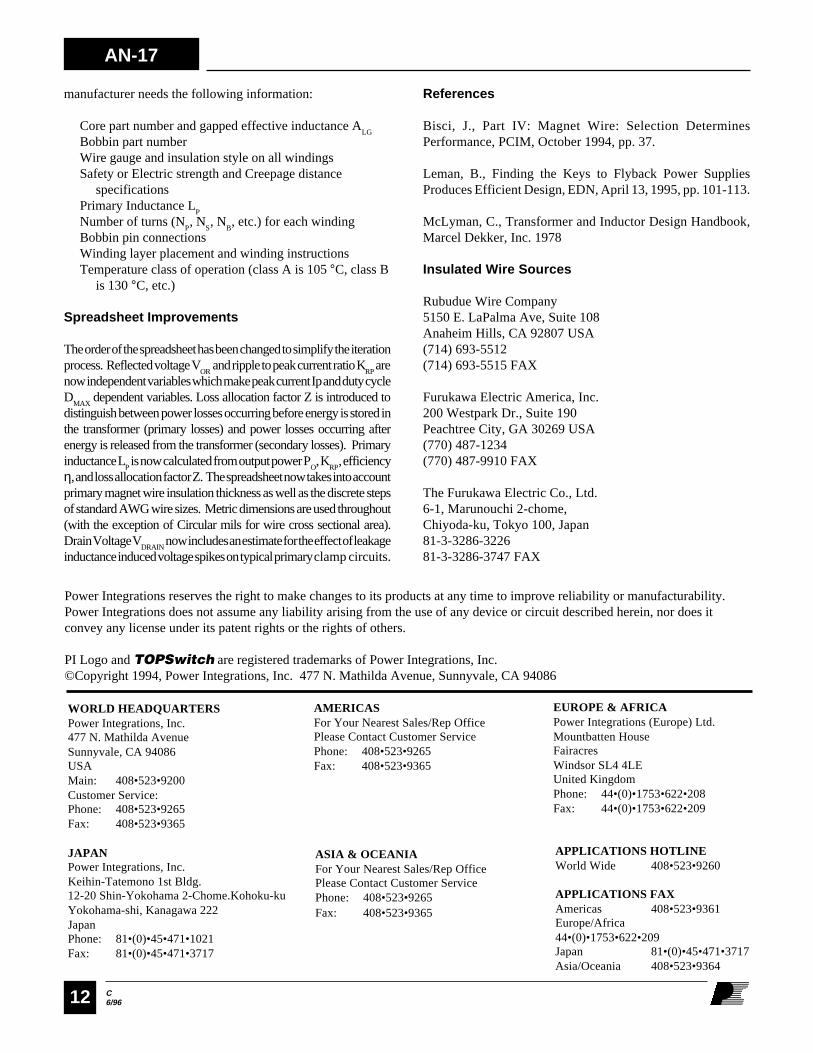
Figure 7. Bridge AC Current, AC Voltage, and DC Voltage Waveforms.
normally used and VD is typically 0.7 Volts.
Bias winding diode forward voltage drop (VDB) is also typically0.7 Volts
Ripple current to peak current ratio KRP determines how far intothe continuous mode a flyback transformer will operate.Continuous mode transformers optimized for TOPSwitchapplications operating from 100/115 VAC or universal inputvoltage should have a minimum KRP of 0.4. Applicationsoperating from 230 VAC input voltage should have a minimumKRP of 0.6. Discontinuous mode transformers optimized forTOPSwitch applications always have a KRP equal to 1.0.
KI
IRPR
P
=
Transformer Core/Construction Variables:
The following effective parameters are specified by the coreand bobbin manufacturer in data sheets: cross sectional area A
e
(cm2), path length Le (cm), ungapped inductance A
L (specified
in either mH/(1000 turns)2 or nH/T2), and physical bobbinwinding width B
W (mm).
Margin width M, determined by insulation methods andregulatory requirements discussed above, is usually between2.5 to 3.0 mm for margin wound or set to zero for insulated wirewound transformers.
For number of layers L, one or two layers of primary windingare normally used. Higher number of layers increase cost,increase capacitance, reduce coupling, and increase leakageinductance.

AN-17
C6/968
Number of secondary turns NS is a key iteration variable. One
turn per Volt of output voltage is a good value to begin with forN
S (for example: start with 5 turns for a +5V output).
The four groups of dependent parameters can now be calculated.
DC Input Voltage Parameters:
Minimum DC input voltage VMIN
depends on the AC inputvoltage, bridge rectifier, and energy storage capacitor.Figure 7 shows how C
IN charges to the peak of the AC input
voltage during a short conduction time tC. Because of full wave
rectification, CIN
has a ripple voltage at twice line frequency.C
IN must supply the entire average primary current during the
discharge time between the peaks of the AC input voltage.Minimum DC voltage V
MIN can be found from the following
equation where PO is the power supply output power, η is an
estimate of efficiency, fL is line voltage frequency, V
ACMIN is the
minimum AC mains voltage, CIN
is the value of the filtercapacitor, and t
C is an estimate for conduction time. As an
example, for 60 Hz, 85 VAC input voltage, efficiency of 0.8,15 Watt output power, 33 uF input filter capacitance, andestimated conduction time of 3.2 mS, V
MIN is 93 Volts DC.
V VP
ft
CMIN ACMIN
OL
C
IN
= × −× ×
×−
×( ) (
( ))2
21
22
η
= × −× ×
×−
×=( ) (
( . )
.)2 85
2 151
2 603 2
0 8 33932
mS
FV
µ
Maximum DC input voltageVMAX
is simply the peak value ofthe highest AC input voltage (V
ACMAX) expected in the
application. Operation from 265 VAC input results in amaximum DC bus voltage V
MAX of 375 Volts DC.
V V VMAX ACMAX= × = × =2 265 2 375
Current Waveform Shape Parameters:
DMAX
is the actual duty cycle occurring when the TOPSwitchpower supply delivers maximum output power from minimuminput voltage. D
MAX has an upper limit equal to the minimum
value of the TOPSwitch Data Sheet parameter DCMAX
(64%).D
MAX is calculated from reflected voltage V
OR, minimum DC
input voltage VMIN
, and TOPSwitch on-state Drain to Source
voltage VDS
:
DV
V V VMAXOR
OR MIN DS
=+ −( )
Average current IAVG
is calculated from minimum DC input
voltage VMIN
, output power PO, and efficiency η:
IP
VAVGO
MIN
=×η
Peak primary current Ip is calculated from average current IAVG
,ripple to peak current ratio K
RP, and maximum duty cycle D
MAX:
I IK DP AVG
RP MAX
= ×− ×
22( )
Ripple current IR is calculated from average current IAVG, peakprimary current IP, and maximum duty cycle DMAX:
I II
DR PAVG
MAX
= × −2 ( )
RMS current IRMS
is calculated from maximum duty cycle DMAX
,peak primary current I
P, and ripple to peak ratio K
RP. I
RMS can
also be calculated directly from DMAX
, IP, and ripple current I
R.
I I DK
KRMS P MAXRP
RP= × × − +( )2
31
= × − × +D I I II
MAX P P RR( ( ) )22
3
Transformer Design Parameters:
Primary inductance LP (in µH) is determined by the flyback
transformer energy equation defined below. The flybacktransformer stores energy proportional to the square of primarycurrent. When TOPSwitch is on, primary current linearly rampsup over a current range, defined earlier as ripple current I
R, and
increases the energy stored in the flyback transformer core.When TOPSwitch turns off, the stored energy incrementassociated with ripple current I
R is delivered to the load and
secondary losses (rectifier and clamp). Inductance LP can now
by calculated from output power PO, efficiency η, loss allocation
factor Z, peak current IP, switching frequency f
S, and ripple
current to peak current ratio KRP
(which determines IR).

C6/96
AN-17
9
LP
Z
f I KKP
O
S P RPRP
= ×× × − +
× × × −10
1
12
6
2
(( ( ))
)
( )
η ηη
Primary inductance LP (in µH) can also be determined from asimple function of ripple current IR, effective primary voltage(VMIN-VDS), maximum duty cycle DMAX, and switching frequencyfS as shown below but the resulting value for primary inductancemay be slightly different due to the selected value for lossallocation factor Z and TOPSwitch on-state Drain to Sourcevoltage VDS. The energy equation given above is preferred forselecting the value of inductance LP while the ripple currentequation given below is best for verifying the LP value usingin-circuit measurements.
LV V D
I fP MEASUREDMIN DS MAX
R S( )
( )= × − ××
106
Number of primary turns NP depends on number of secondary
turns NS, output voltage V
O, diode forward voltage drop V
D,
effective primary voltage (VMIN
-VDS
), and maximum duty cycleD
MAX:
N NV V
V V
D
DP SMIN DS
O D
MAX
MAX
= × −+
×−1
The number of bias winding turns NB is calculated from theoutput voltage VO, output diode voltage VD, secondary numberof turns NS, target bias voltage VB, and bias diode voltage VBD:
NV V
V VNB
B BD
O DS=
++
×
ALG
is the effective inductance for the gapped core in nH/T2.Some core vendors offer standard gapped core sets with specifiedA
LG. The transformer manufacturer either procures the gapped
core for the given ALG
value or grinds the gap to meet theinductance specification in the finished transformer. A
LG is
also used to simplify subsequent calculations. ALG
is calculatedfrom primary inductance L
P (in µH) and number of primary
turns NP. Note that A
LG is specified in nH/(turn)2.
AL
NLGP
P
= ×10002
Maximum flux density BM is a dependent iteration variable to
be manipulated between the limits of 2000 and 3000 Gauss byvarying number of secondary turns N
S which directly varies
number of primary turns NP as previously shown. B
M is
calculated from peak current IP, number of primary turns N
P,
effective gapped inductance ALG
, and effective core crosssectional area A
e. B
M can also be calculated from effective
primary voltage (VMIN
-VDS
), output voltage VO, output diode
voltage VD, and maximum duty cycle D
MAX:
BN I A
AMP P LG
e
= × ××10
= × ××
× −+
×−
NI A
A
V V
V V
D
DSP LG
e
MIN DS
O D
MAX
MAX10 1
BAC is the AC flux density component. The equation gives peakAC flux density (rather than peak to peak) to use with core losscurves provided by the core vendor. BAC can be calculated frommaximum flux density BM and ripple to peak current ratio KRP.BAC can also be calculated from effective primary voltage(VMIN-VDS), duty cycle, frequency, effective core cross sectionalarea, and number of primary turns NP:
BB K V V D
f A NACM RP MIN DS MAX
S e P
= × = − × ×× × ×2
102
8( )
Relative permeability µr of the ungapped core must be calculated
to estimate the gap length Lg. µ
r is found from core parameters
Ae (cm2), L
e (cm), and ungapped effective inductance A
L:
µπrL E
e
A L
A= ×
× × ×0 4 10.
Gap length Lg is the air gap ground into the center leg of the
transformer core. Grinding tolerances and ALG
accuracy placea minimum limit of 0.051 mm on L
g. L
g (in mm) is calculated
from number of primary turns NP, core effective cross sectional
area Ae, primary inductance L
P (in µH), core effective path
length Le, and relative permeability µ
r:
LN A
L
Lg
P e
P
e
r
= × × ××
−
×0 4100
102. π
µEffective bobbin width BW
E takes into account physical bobbin
width BW, margins M, and number of layers L:
BW L BW ME = × − ×( ( ))2

AN-17
C6/9610
CMACM
IRMS
=
This completes all calculations necessary for the primarywinding. Secondary peak current, RMS current, average outputcurrent, output capacitor ripple current, and secondary minimumand maximum conductor diameter must also be calculated.
Peak secondary current ISP
is a simple function of peak primarycurrent I
P, primary turns N
P, and secondary turns N
S.
I IN
NSP PP
S
= ×
Secondary RMS current ISRMS
is found from maximum dutycycle D
MAX, secondary peak current I
SP, and ripple to peak
current ratio KRP
(KRP
is identical for primary and secondary).
I I DK
KSRMS SP MAXRP
RP= × − × − +( ) ( )13
12
Output current IO is simply the ratio of output power P
O to output
Voltage VO:
IP
VOO
O
=
Output capacitor ripple current IRIPPLE
is not a true transformerparameter but is needed for capacitor selection and easy tocalculate from other transformer parameters. I
RIPPLE is found
from secondary RMS current ISRMS
and output current IO.
I I IRIPPLE SRMS O= −2 2
Minimum secondary bare conductor diameter DIAS (in mm)
based on previously calculated current capacity CMA and
secondary RMS current must be determined.
From the primary CMA and secondary RMS current ISRMS
, theminimum secondary bare conductor CM
S is calculated.
CM CMA IS SRMS= ×
Minimum secondary AWGS is then calculated from another
empirical equation. Secondary calculated wire gauge AWGS is
always rounded down to the next integer value which selects thenext larger standard wire size.
Primary insulated wire diameter OD in mm is found fromeffective bobbin width BW
E and number of primary turns N
P:
ODBW
NE
P
=
The bias winding is usually wound with the same wire diameteras the primary to reduce the number of different wire gaugesnecessary for production.
Actual magnet wire outside diameter OD is slightly larger thanthe diameter DIA of the bare copper conductor. Insulationthickness varies inversely with bare copper conductor AmericanWire Gauge (AWG) size which means that smaller diameterconductors have thinner insulation thickness. Data from severaldifferent manufacturers were tabulated to generate an empiricalexpression for total insulation thickness INS (in mm) as afunction of heavy insulated magnet wire outside diameter(in mm).
INS LOG OD= × +( . ( )) .0 0594 0 0834
DIA OD INS= −
Another empirical equation determines the AWG for magnetwire with a given bare conductor diameter DIA. Integer AWGvalues are the standard sizes of available wire so the calculatedAWG value should always be rounded up to the next integer orstandard value (the next smaller standard conductor diameter)before proceeding with the current capacity or CMA calculation.
AWG LOG DIA= × − ×9 97 1 8277 2. ( . ( ( )))
Magnet wire for transformer winding usually has the crosssectional area specified in circular mils. A circular mil is thecross sectional area of a wire with a diameter of 1 mil (or0.0254 mm). The effective cross sectional area in circular mils(CM) of a standard AWG size bare conductor wire is foundfrom the following simple expression.
CMAWG
=−
2
503
“Circular mils per Amp” or CMA is a convenient way to specifywinding current capacity. CMA, which is the inverse of currentdensity, is simply the ratio of cross sectional area in circularmils to the RMS value of primary current. CMA should bebetween 200 and 500 and is calculated from cross sectionalwire area in CM and RMS primary current I
RMS.

C6/96
AN-17
11
AWG LOG CMS S= × −9 97 5 017. ( . ( ))
(Secondary conductors larger than 26 AWG should not be useddue to skin effects. Refer to AN-18 for suggestions on parallelconductor techniques.)
Bare conductor diameter (in mm) is now determined.
DIAS
AWGS
= ××
×−
4 21 27
25 41000
503
..
π
The maximum wire outside diameter ODS (in mm) for a single
layer based on number of secondary turns and bobbin widthmust also be calculated:
ODBW M
NSS
= − ×( )2
Secondary wire insulation thickness can now be calculatedfrom the bare conductor outside diameter (determined byCMA) and the insulated wire outside diameter (determined bynumber of turns and effective bobbin width). Note that secondaryinsulation thickness INS
S (in mm) is the insulation wall thickness
rather than the total insulation thickness used in the primarywinding calculation.
INSOD DIA
SS S= −
2
Obviously, if insulation thickness INSS is not a positive number,
another transformer design iteration is necessary with eithermore secondary layers, a smaller number of secondary turns, ora transformer core with a wider bobbin.
For insulated wire secondaries, INSS must be equal to or greater
than insulation thickness of the selected wire.
Parallel combinations of wire with half the diameter may beeasier to wind and terminate but the effective secondary CMAwill be half the value of the single winding.
Voltage Stress Parameters:
Maximum drain voltage is the sum of maximum DC inputvoltage V
MAX, an estimated drain clamp voltage term based on
VOR
, and an estimated voltage term related to typical blockingdiode forward recovery. Refer to AN-16 for more detail.
V V V VDRAIN MAX OR= + × × +( . . )1 4 1 5 20
Maximum peak inverse voltage PIVS for the output rectifier is
determined by transformer primary and secondary number ofturns N
P and N
S, maximum DC input voltage V
MAX, and output
voltage VO.
PIV V VN
NS O MAXS
P
= + ×( )
Maximum peak inverse voltage PIVB for the bias rectifier is
determined from a similar equation using number of bias turnsN
B.
PIV V VN
NB B MAXB
P
= + ×( )
Additional or auxiliary output winding number of turns NX andrectifier diode peak inverse voltage PIVX can be determinedfrom the desired value for auxiliary output voltage VX, auxiliaryrectifier diode forward voltage drop VDX, output voltage VO,output rectifier diode forward voltage drop VD, and number ofsecondary turns NS.
NV V
V VNX
X DX
O DS= +
+×
PIV V VN
NX X MAXX
P
= + ×( )
Iteration can now be used to reach a final and acceptablesolution for the flyback transformer design.
Iterate number of secondary turns NS or primary ripple to peakcurrent ratio KRP until maximum flux density BM is betweenindicated limits and check that gap length Lg is higher thanindicated minimum value. BM will decrease and Lg will increaseas NS or KRP is increased.
Examine primary current capacity in Circular Mils per Amp(CMA). If CMA is below the specified lower limit of 200,consider increasing number of primary layers from one to twoor use the next larger core size and perform new iteration. IfCMA is greater than 500, consider using the next smaller coresize. (CMA greater than 500 simply means that the wirediameter is oversized for the expected RMS current).
The transformer design is now complete. The transformer
AN-17
C6/9612
manufacturer needs the following information:
Core part number and gapped effective inductance ALG
Bobbin part numberWire gauge and insulation style on all windingsSafety or Electric strength and Creepage distance
specificationsPrimary Inductance L
P
Number of turns (NP, N
S, N
B, etc.) for each winding
Bobbin pin connectionsWinding layer placement and winding instructionsTemperature class of operation (class A is 105 °C, class B
is 130 °C, etc.)
Spreadsheet Improvements
The order of the spreadsheet has been changed to simplify the iterationprocess. Reflected voltage V
OR and ripple to peak current ratio K
RP are
now independent variables which make peak current Ip and duty cycleD
MAX dependent variables. Loss allocation factor Z is introduced to
distinguish between power losses occurring before energy is stored inthe transformer (primary losses) and power losses occurring afterenergy is released from the transformer (secondary losses). Primaryinductance L
P is now calculated from output power P
O, K
RP, efficiency
η, and loss allocation factor Z. The spreadsheet now takes into accountprimary magnet wire insulation thickness as well as the discrete stepsof standard AWG wire sizes. Metric dimensions are used throughout(with the exception of Circular mils for wire cross sectional area).Drain Voltage V
DRAIN now includes an estimate for the effect of leakage
inductance induced voltage spikes on typical primary clamp circuits.
References
Bisci, J., Part IV: Magnet Wire: Selection DeterminesPerformance, PCIM, October 1994, pp. 37.
Leman, B., Finding the Keys to Flyback Power SuppliesProduces Efficient Design, EDN, April 13, 1995, pp. 101-113.
McLyman, C., Transformer and Inductor Design Handbook,Marcel Dekker, Inc. 1978
Insulated Wire Sources
Rubudue Wire Company5150 E. LaPalma Ave, Suite 108Anaheim Hills, CA 92807 USA(714) 693-5512(714) 693-5515 FAX
Furukawa Electric America, Inc.200 Westpark Dr., Suite 190Peachtree City, GA 30269 USA(770) 487-1234(770) 487-9910 FAX
The Furukawa Electric Co., Ltd.6-1, Marunouchi 2-chome,Chiyoda-ku, Tokyo 100, Japan81-3-3286-322681-3-3286-3747 FAX
Power Integrations reserves the right to make changes to its products at any time to improve reliability or manufacturability.Power Integrations does not assume any liability arising from the use of any device or circuit described herein, nor does itconvey any license under its patent rights or the rights of others.
PI Logo and TOPSwitch are registered trademarks of Power Integrations, Inc.©Copyright 1994, Power Integrations, Inc. 477 N. Mathilda Avenue, Sunnyvale, CA 94086
JAPANPower Integrations, Inc.Keihin-Tatemono 1st Bldg.12-20 Shin-Yokohama 2-Chome.Kohoku-kuYokohama-shi, Kanagawa 222JapanPhone: 81•(0)•45•471•1021Fax: 81•(0)•45•471•3717
ASIA & OCEANIAFor Your Nearest Sales/Rep OfficePlease Contact Customer ServicePhone: 408•523•9265Fax: 408•523•9365
WORLD HEADQUARTERSPower Integrations, Inc.477 N. Mathilda AvenueSunnyvale, CA 94086USAMain: 408•523•9200Customer Service:Phone: 408•523•9265Fax: 408•523•9365
AMERICASFor Your Nearest Sales/Rep OfficePlease Contact Customer ServicePhone: 408•523•9265Fax: 408•523•9365
APPLICATIONS HOTLINEWorld Wide 408•523•9260
APPLICATIONS FAXAmericas 408•523•9361Europe/Africa44•(0)•1753•622•209Japan 81•(0)•45•471•3717Asia/Oceania 408•523•9364
EUROPE & AFRICAPower Integrations (Europe) Ltd.Mountbatten HouseFairacresWindsor SL4 4LEUnited KingdomPhone: 44•(0)•1753•622•208Fax: 44•(0)•1753•622•209

专注于微波、射频、天线设计人才的培养 易迪拓培训 网址:http://www.edatop.com
射 频 和 天 线 设 计 培 训 课 程 推 荐
易迪拓培训(www.edatop.com)由数名来自于研发第一线的资深工程师发起成立,致力并专注于微
波、射频、天线设计研发人才的培养;我们于 2006 年整合合并微波 EDA 网(www.mweda.com),现
已发展成为国内最大的微波射频和天线设计人才培养基地,成功推出多套微波射频以及天线设计经典
培训课程和 ADS、HFSS 等专业软件使用培训课程,广受客户好评;并先后与人民邮电出版社、电子
工业出版社合作出版了多本专业图书,帮助数万名工程师提升了专业技术能力。客户遍布中兴通讯、
研通高频、埃威航电、国人通信等多家国内知名公司,以及台湾工业技术研究院、永业科技、全一电
子等多家台湾地区企业。
易迪拓培训课程列表:http://www.edatop.com/peixun/rfe/129.html
射频工程师养成培训课程套装
该套装精选了射频专业基础培训课程、射频仿真设计培训课程和射频电
路测量培训课程三个类别共 30 门视频培训课程和 3 本图书教材;旨在
引领学员全面学习一个射频工程师需要熟悉、理解和掌握的专业知识和
研发设计能力。通过套装的学习,能够让学员完全达到和胜任一个合格
的射频工程师的要求…
课程网址:http://www.edatop.com/peixun/rfe/110.html
ADS 学习培训课程套装
该套装是迄今国内最全面、最权威的 ADS 培训教程,共包含 10 门 ADS
学习培训课程。课程是由具有多年 ADS 使用经验的微波射频与通信系
统设计领域资深专家讲解,并多结合设计实例,由浅入深、详细而又
全面地讲解了 ADS 在微波射频电路设计、通信系统设计和电磁仿真设
计方面的内容。能让您在最短的时间内学会使用 ADS,迅速提升个人技
术能力,把 ADS 真正应用到实际研发工作中去,成为 ADS 设计专家...
课程网址: http://www.edatop.com/peixun/ads/13.html
HFSS 学习培训课程套装
该套课程套装包含了本站全部 HFSS 培训课程,是迄今国内最全面、最
专业的HFSS培训教程套装,可以帮助您从零开始,全面深入学习HFSS
的各项功能和在多个方面的工程应用。购买套装,更可超值赠送 3 个月
免费学习答疑,随时解答您学习过程中遇到的棘手问题,让您的 HFSS
学习更加轻松顺畅…
课程网址:http://www.edatop.com/peixun/hfss/11.html
`

专注于微波、射频、天线设计人才的培养 易迪拓培训 网址:http://www.edatop.com
CST 学习培训课程套装
该培训套装由易迪拓培训联合微波 EDA 网共同推出,是最全面、系统、
专业的 CST 微波工作室培训课程套装,所有课程都由经验丰富的专家授
课,视频教学,可以帮助您从零开始,全面系统地学习 CST 微波工作的
各项功能及其在微波射频、天线设计等领域的设计应用。且购买该套装,
还可超值赠送 3 个月免费学习答疑…
课程网址:http://www.edatop.com/peixun/cst/24.html
HFSS 天线设计培训课程套装
套装包含 6 门视频课程和 1 本图书,课程从基础讲起,内容由浅入深,
理论介绍和实际操作讲解相结合,全面系统的讲解了 HFSS 天线设计的
全过程。是国内最全面、最专业的 HFSS 天线设计课程,可以帮助您快
速学习掌握如何使用 HFSS 设计天线,让天线设计不再难…
课程网址:http://www.edatop.com/peixun/hfss/122.html
13.56MHz NFC/RFID 线圈天线设计培训课程套装
套装包含 4 门视频培训课程,培训将 13.56MHz 线圈天线设计原理和仿
真设计实践相结合,全面系统地讲解了 13.56MHz线圈天线的工作原理、
设计方法、设计考量以及使用 HFSS 和 CST 仿真分析线圈天线的具体
操作,同时还介绍了 13.56MHz 线圈天线匹配电路的设计和调试。通过
该套课程的学习,可以帮助您快速学习掌握 13.56MHz 线圈天线及其匹
配电路的原理、设计和调试…
详情浏览:http://www.edatop.com/peixun/antenna/116.html
我们的课程优势:
※ 成立于 2004 年,10 多年丰富的行业经验,
※ 一直致力并专注于微波射频和天线设计工程师的培养,更了解该行业对人才的要求
※ 经验丰富的一线资深工程师讲授,结合实际工程案例,直观、实用、易学
联系我们:
※ 易迪拓培训官网:http://www.edatop.com
※ 微波 EDA 网:http://www.mweda.com
※ 官方淘宝店:http://shop36920890.taobao.com
专注于微波、射频、天线设计人才的培养
官方网址:http://www.edatop.com 易迪拓培训 淘宝网店:http://shop36920890.taobao.com


![U-165 Reference Design: Isolated 50 Watt Flyback Converter ...Transformer Design [2] The transformer in a flyback converter is actually a coupled inductor with multiple windings. Trans-formers](https://img.pdfslide.net/doc/110x75/6067efcf513c1477013c4438/u-165-reference-design-isolated-50-watt-flyback-converter-transformer-design.jpg)


![Catalogue FLYBACK Equivalent - [PDF Document] FLYBACK Equivalent FlyBack Equivalent flyback reemplazo conversor Flyback tv fly-back Flyback Tester Flyback Converter conversor Flyback](https://img.pdfslide.net/doc/110x75/5a832a447f8b9a9d308e9416/catalogue-flyback-equivalent-pdf-document-flyback-equivalent-flyback-equivalent.jpg)