Embed Size (px)
Citation preview

Slide Set 7for ENEL 353 Fall 2015
Steve Norman, PhD, PEng
Electrical & Computer EngineeringSchulich School of Engineering
University of Calgary
Fall Term, 2015
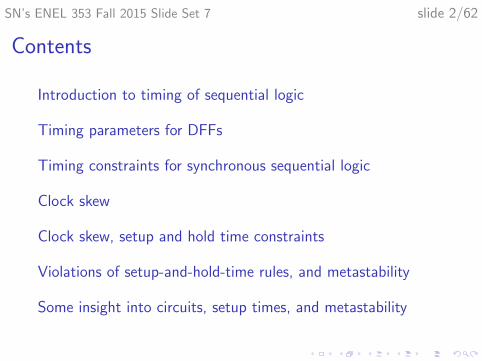
SN’s ENEL 353 Fall 2015 Slide Set 7 slide 2/62
Contents
Introduction to timing of sequential logic
Timing parameters for DFFs
Timing constraints for synchronous sequential logic
Clock skew
Clock skew, setup and hold time constraints
Violations of setup-and-hold-time rules, and metastability
Some insight into circuits, setup times, and metastability
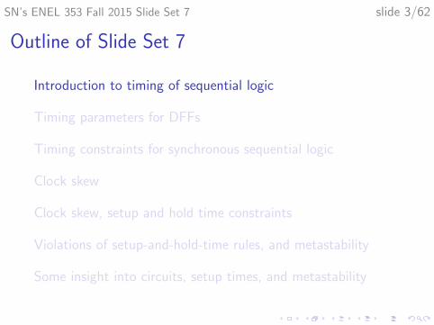
SN’s ENEL 353 Fall 2015 Slide Set 7 slide 3/62
Outline of Slide Set 7
Introduction to timing of sequential logic
Timing parameters for DFFs
Timing constraints for synchronous sequential logic
Clock skew
Clock skew, setup and hold time constraints
Violations of setup-and-hold-time rules, and metastability
Some insight into circuits, setup times, and metastability
SN’s ENEL 353 Fall 2015 Slide Set 7 slide 4/62
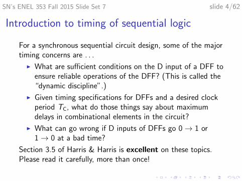
Introduction to timing of sequential logic
For a synchronous sequential circuit design, some of the majortiming concerns are . . .
I What are sufficient conditions on the D input of a DFF toensure reliable operations of the DFF? (This is called the“dynamic discipline”.)
I Given timing specifications for DFFs and a desired clockperiod TC, what do those things say about maximumdelays in combinational elements in the circuit?
I What can go wrong if D inputs of DFFs go 0→ 1 or1→ 0 at a bad time?
Section 3.5 of Harris & Harris is excellent on these topics.Please read it carefully, more than once!

SN’s ENEL 353 Fall 2015 Slide Set 7 slide 5/62
Review: The static discipline
This idea was introduced very early in the course. (SeeSection 1.6 of Harris and Harris.)
The static discipline says that for reliable operation of digitalcircuit elements, voltages on inputs of circuit elements mustnot sit in the forbidden zone between VIL and VIH.
(Of course, voltages are allowed to pass through the forbiddenzone when making low-to-high or high-to-low transitions!)
SN’s ENEL 353 Fall 2015 Slide Set 7 slide 6/62
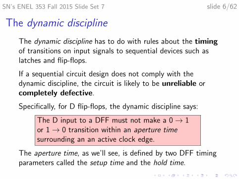
The dynamic discipline
The dynamic discipline has to do with rules about the timingof transitions on input signals to sequential devices such aslatches and flip-flops.
If a sequential circuit design does not comply with thedynamic discipline, the circuit is likely to be unreliable orcompletely defective.
Specifically, for D flip-flops, the dynamic discipline says:
The D input to a DFF must not make a 0→ 1or 1→ 0 transition within an aperture timesurrounding an an active clock edge.
The aperture time, as we’ll see, is defined by two DFF timingparameters called the setup time and the hold time.
SN’s ENEL 353 Fall 2015 Slide Set 7 slide 7/62
Outline of Slide Set 7
Introduction to timing of sequential logic
Timing parameters for DFFs
Timing constraints for synchronous sequential logic
Clock skew
Clock skew, setup and hold time constraints
Violations of setup-and-hold-time rules, and metastability
Some insight into circuits, setup times, and metastability
SN’s ENEL 353 Fall 2015 Slide Set 7 slide 8/62
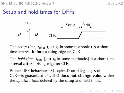
Setup and hold times for DFFs
D Q
CLK
CLK
tsetup thold
The setup time, tsetup (just ts in some textbooks) is a shorttime interval before a rising edge on CLK.
The hold time, thold (just th in some textbooks) is a short timeinterval after a rising edge on CLK.
Proper DFF behaviour—Q copies D on rising edges ofCLK—is guaranteed only if D does not change value withinthe aperture time defined by the setup and hold times.
SN’s ENEL 353 Fall 2015 Slide Set 7 slide 9/62
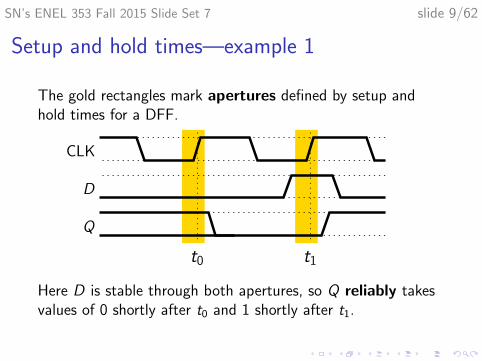
Setup and hold times—example 1
The gold rectangles mark apertures defined by setup andhold times for a DFF.
CLK
D
Q
t0 t1
Here D is stable through both apertures, so Q reliably takesvalues of 0 shortly after t0 and 1 shortly after t1.
SN’s ENEL 353 Fall 2015 Slide Set 7 slide 10/62
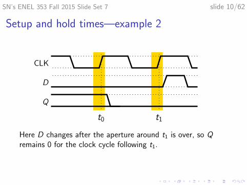
Setup and hold times—example 2
CLK
D
Q
t0 t1
Here D changes after the aperture around t1 is over, so Qremains 0 for the clock cycle following t1.
SN’s ENEL 353 Fall 2015 Slide Set 7 slide 11/62
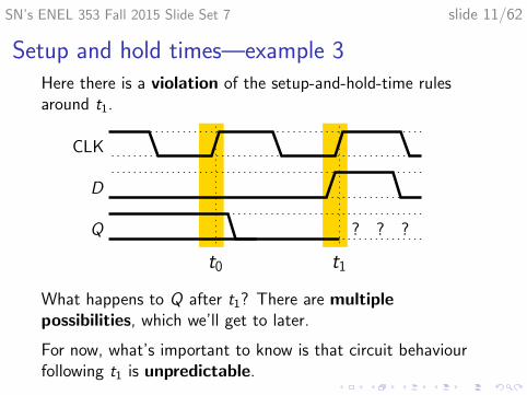
Setup and hold times—example 3Here there is a violation of the setup-and-hold-time rulesaround t1.
CLK
D
Q
t0 t1
? ? ?
What happens to Q after t1? There are multiplepossibilities, which we’ll get to later.
For now, what’s important to know is that circuit behaviourfollowing t1 is unpredictable.

SN’s ENEL 353 Fall 2015 Slide Set 7 slide 12/62
D flip-flop clock-to-Q delays: tccq and tpcq
D Q
CLK As mentioned several lectures ago, the Qoutput of a DFF does not change at exactlythe same time as its input CLK signalrises—there is a short delay.
tccq is the clock-to-Q contamination delay. It takes at leastthis much time for a rising edge of CLK to cause a changein Q.
tpcq is the clock-to-Q propagation delay. It takes no morethan this much time for a rising edge of CLK to cause achange in Q.
SN’s ENEL 353 Fall 2015 Slide Set 7 slide 13/62
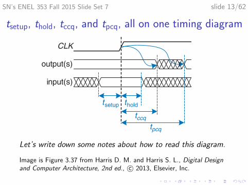
tsetup, thold, tccq, and tpcq, all on one timing diagram
CLK
tccq
tpcq
t setup
output(s)
input(s)
t hold
Let’s write down some notes about how to read this diagram.
Image is Figure 3.37 from Harris D. M. and Harris S. L., Digital Designand Computer Architecture, 2nd ed., c© 2013, Elsevier, Inc.
SN’s ENEL 353 Fall 2015 Slide Set 7 slide 14/62
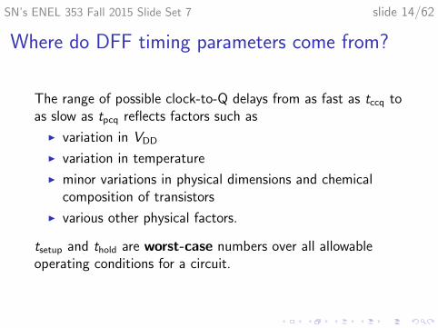
Where do DFF timing parameters come from?
The range of possible clock-to-Q delays from as fast as tccq toas slow as tpcq reflects factors such as
I variation in VDD
I variation in temperature
I minor variations in physical dimensions and chemicalcomposition of transistors
I various other physical factors.
tsetup and thold are worst-case numbers over all allowableoperating conditions for a circuit.

SN’s ENEL 353 Fall 2015 Slide Set 7 slide 15/62
Remark about resettable, settable, and enabled
flip-flops
The textbook doesn’t mention this, but it’s good to know.
For DFFs with EN inputs, and/or synchronous reset or setinputs, the EN, reset and set inputs have tsetup and tholdparameters that are similar to the tsetup and thold parametersfor the D input.
For DFFs with asynchronous reset or set inputs, the timingparameters for those inputs are typically a minimum widthfor a reset or set pulse, along with a minimum gap betweenwhen reset or set is turned off and a rising edge of the clock.

SN’s ENEL 353 Fall 2015 Slide Set 7 slide 16/62
Outline of Slide Set 7
Introduction to timing of sequential logic
Timing parameters for DFFs
Timing constraints for synchronous sequential logic
Clock skew
Clock skew, setup and hold time constraints
Violations of setup-and-hold-time rules, and metastability
Some insight into circuits, setup times, and metastability
SN’s ENEL 353 Fall 2015 Slide Set 7 slide 17/62
Timing constraints for synchronous sequential logic
We have now been introduced to the DFF timing parameterstsetup, thold tccq, and tpcq.
We’re about to put those ideas together with earlier ideasabout timing of combinational logic.
The results will be some inequalities that will help us assesswhether synchronous sequential designs are safe withrespect to timing.
SN’s ENEL 353 Fall 2015 Slide Set 7 slide 18/62
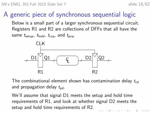
A generic piece of synchronous sequential logicBelow is a small part of a larger synchronous sequential circuit.Registers R1 and R2 are collections of DFFs that all have thesame tsetup, thold, tccq, and tpcq.
CL
CLK
R2R1
Q1D1 Q2D2
The combinational element shown has contamination delay tcdand propagation delay tpd.
We’ll assume that signal D1 meets the setup and hold timerequirements of R1, and look at whether signal D2 meets thesetup and hold time requirements of R2.
SN’s ENEL 353 Fall 2015 Slide Set 7 slide 19/62
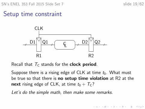
Setup time constraint
CL
CLK
R2R1
Q1D1 Q2D2
Recall that TC stands for the clock period.
Suppose there is a rising edge of CLK at time t0. What mustbe true so that there is no setup time violation at R2 at thenext rising edge of CLK, at time t0 + TC?
Let’s do the simple math, then make some remarks.
SN’s ENEL 353 Fall 2015 Slide Set 7 slide 20/62
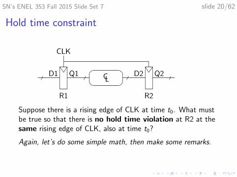
Hold time constraint
CL
CLK
R2R1
Q1D1 Q2D2
Suppose there is a rising edge of CLK at time t0. What mustbe true so that there is no hold time violation at R2 at thesame rising edge of CLK, also at time t0?
Again, let’s do some simple math, then make some remarks.
SN’s ENEL 353 Fall 2015 Slide Set 7 slide 21/62
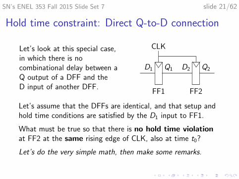
Hold time constraint: Direct Q-to-D connection
Let’s look at this special case,in which there is nocombinational delay between aQ output of a DFF and theD input of another DFF.
Q1D1
CLK
FF1 FF2
D2 Q2
Let’s assume that the DFFs are identical, and that setup andhold time conditions are satisfied by the D1 input to FF1.
What must be true so that there is no hold time violationat FF2 at the same rising edge of CLK, also at time t0?
Let’s do the very simple math, then make some remarks.
SN’s ENEL 353 Fall 2015 Slide Set 7 slide 22/62
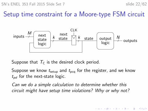
Setup time constraint for a Moore-type FSM circuit
outputlogic
nextstatelogic
statenext
statek kM
Ninputsoutputs
CLK
Suppose that TC is the desired clock period.
Suppose we know tsetup and tpcq for the register, and we knowtpd for the next-state logic.
Can we do a simple calculation to determine whether thiscircuit might have setup time violations? Why or why not?
SN’s ENEL 353 Fall 2015 Slide Set 7 slide 23/62
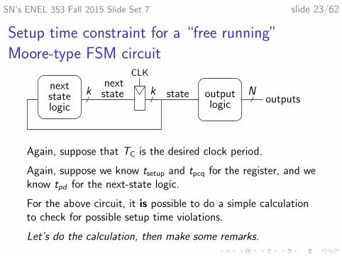
Setup time constraint for a “free running”
Moore-type FSM circuit
outputlogic
nextstatelogic
statenext
statek k Noutputs
CLK
Again, suppose that TC is the desired clock period.
Again, suppose we know tsetup and tpcq for the register, and weknow tpd for the next-state logic.
For the above circuit, it is possible to do a simple calculationto check for possible setup time violations.
Let’s do the calculation, then make some remarks.

SN’s ENEL 353 Fall 2015 Slide Set 7 slide 24/62
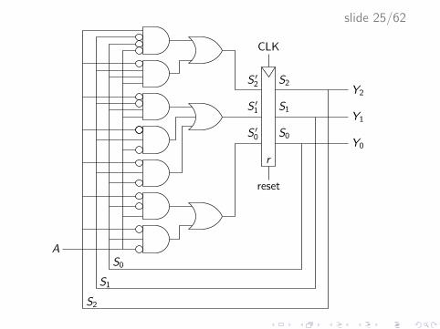
Synchronous logic timing: Detailed example
Suppose A is connected to VDD inthe circuit on the next slide.
Bubbles on the AND gate inputs areimplemented using NOT gates.
For the register, tsetup = 35 ps andtpcq = 75 ps.
Is it safe to run the clock with afrequency of 3.33 GHz?
If not, what is a simple redesign thatwould allow safe operation at3.33 GHz?
gate tpd (ps)NOT 30NAND2 40NAND3 60NAND4 80AND2 60AND3 80AND4 100OR2 80OR3 110
slide 25/62
A
S ′2
Y2
S2
Y1
Y0
S1S ′1
S ′0 S0
CLK
reset
r
S0
S1
S2
SN’s ENEL 353 Fall 2015 Slide Set 7 slide 26/62
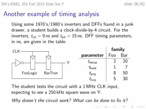
Another example of timing analysis
Using some 1970’s/1980’s inverters and DFFs found in a junkdrawer, a student builds a clock-divide-by-4 circuit. For theinverters, tcd = 9 ns and tpd = 15 ns. DFF timing parameters,in ns, are given in the table.
FooLogic BarTron
CLK
Y
familyparameter Foo Bar
tsetup 2 20thold 1 7tpcq 8 50tccq 5 30
The student tests the circuit with a 1 MHz CLK input,expecting to see a 250 kHz square wave on Y.
Why doesn’t the circuit work? What can be done to fix it?
SN’s ENEL 353 Fall 2015 Slide Set 7 slide 27/62
Outline of Slide Set 7
Introduction to timing of sequential logic
Timing parameters for DFFs
Timing constraints for synchronous sequential logic
Clock skew
Clock skew, setup and hold time constraints
Violations of setup-and-hold-time rules, and metastability
Some insight into circuits, setup times, and metastability
SN’s ENEL 353 Fall 2015 Slide Set 7 slide 28/62
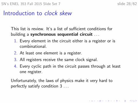
Introduction to clock skew
This list is review. It’s a list of sufficient conditions forbuilding a synchronous sequential circuit . . .
1. Every element in the circuit either is a register or iscombinational.
2. At least one element is a register.
3. All registers receive the same clock signal.
4. Every cyclic path in the circuit passes through at leastone register.
Unfortunately, the laws of physics make it very hard toperfectly satisfy condition 3 . . .
SN’s ENEL 353 Fall 2015 Slide Set 7 slide 29/62
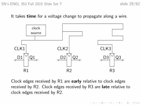
It takes time for a voltage change to propagate along a wire.
clocksource
R1
Q1D1
R2
Q2D2
R3
Q3D3
CLK1 CLK2 CLK3
Clock edges received by R1 are early relative to clock edgesreceived by R2. Clock edges received by R3 are late relative toclock edges received by R2.
SN’s ENEL 353 Fall 2015 Slide Set 7 slide 30/62
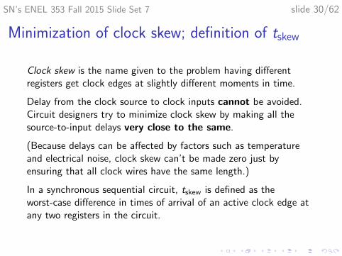
Minimization of clock skew; definition of tskew
Clock skew is the name given to the problem having differentregisters get clock edges at slightly different moments in time.
Delay from the clock source to clock inputs cannot be avoided.Circuit designers try to minimize clock skew by making all thesource-to-input delays very close to the same.
(Because delays can be affected by factors such as temperatureand electrical noise, clock skew can’t be made zero just byensuring that all clock wires have the same length.)
In a synchronous sequential circuit, tskew is defined as theworst-case difference in times of arrival of an active clock edge atany two registers in the circuit.
SN’s ENEL 353 Fall 2015 Slide Set 7 slide 31/62
Outline of Slide Set 7
Introduction to timing of sequential logic
Timing parameters for DFFs
Timing constraints for synchronous sequential logic
Clock skew
Clock skew, setup and hold time constraints
Violations of setup-and-hold-time rules, and metastability
Some insight into circuits, setup times, and metastability

SN’s ENEL 353 Fall 2015 Slide Set 7 slide 32/62
Clock skew, setup and hold time constraints
CLK1 and CLK2 come from the same clock source, but due toclock skew, clock edges might not arrive at R1 and R2 atexactly the same time.
CLQ1D1 Q2D2
R1 R2
CLK1 CLK2
Review: If it happens that that there is no clock skew, thenwe know for safe operation this must be true . . .
tpd for CL ≤ TC − (tpcq + tsetup) (tsetup constraint)
tcd for CL ≥ thold − tccq (thold constraint)
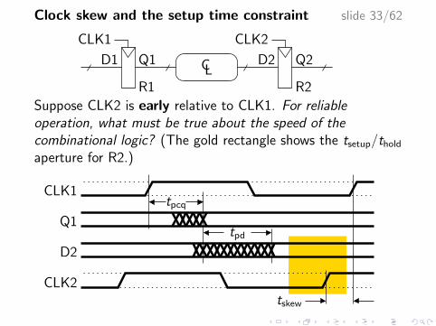
Clock skew and the setup time constraint slide 33/62
CLQ1D1 Q2D2
R1 R2
CLK1 CLK2
Suppose CLK2 is early relative to CLK1. For reliableoperation, what must be true about the speed of thecombinational logic? (The gold rectangle shows the tsetup/tholdaperture for R2.)
CLK1
CLK2
D2
Q1
tpcq
tpd
tskew
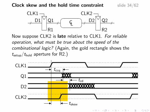
Clock skew and the hold time constraint slide 34/62
CLQ1D1 Q2D2
R1 R2
CLK1 CLK2
Now suppose CLK2 is late relative to CLK1. For reliableoperation, what must be true about the speed of thecombinational logic? (Again, the gold rectangle shows thetsetup/thold aperture for R2.)
CLK1
CLK2
D2
Q1
tskew
tccq
tcd
SN’s ENEL 353 Fall 2015 Slide Set 7 slide 35/62
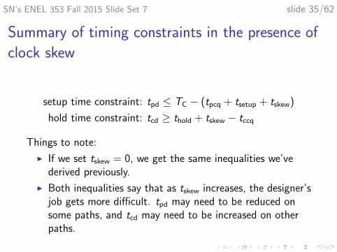
Summary of timing constraints in the presence of
clock skew
setup time constraint: tpd ≤ TC − (tpcq + tsetup + tskew)
hold time constraint: tcd ≥ thold + tskew − tccq
Things to note:
I If we set tskew = 0, we get the same inequalities we’vederived previously.
I Both inequalities say that as tskew increases, the designer’sjob gets more difficult. tpd may need to be reduced onsome paths, and tcd may need to be increased on otherpaths.
SN’s ENEL 353 Fall 2015 Slide Set 7 slide 36/62
Outline of Slide Set 7
Introduction to timing of sequential logic
Timing parameters for DFFs
Timing constraints for synchronous sequential logic
Clock skew
Clock skew, setup and hold time constraints
Violations of setup-and-hold-time rules, and metastability
Some insight into circuits, setup times, and metastability

SN’s ENEL 353 Fall 2015 Slide Set 7 slide 37/62
Review of a simple timing example
Here there is a violation of the setup-and-hold-time rulesaround t1.
CLK
D
Q
t0 t1
? ? ?
What happens to Q after t1? There are multiplepossibilities.
Let’s look at these multiple possibilities in more detail.
SN’s ENEL 353 Fall 2015 Slide Set 7 slide 38/62
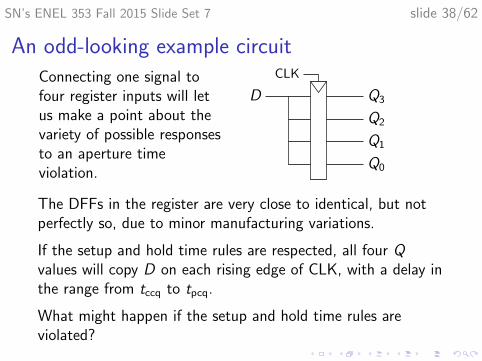
An odd-looking example circuitConnecting one signal tofour register inputs will letus make a point about thevariety of possible responsesto an aperture timeviolation.
Q3
Q2
Q1
Q0
D
CLK
The DFFs in the register are very close to identical, but notperfectly so, due to minor manufacturing variations.
If the setup and hold time rules are respected, all four Qvalues will copy D on each rising edge of CLK, with a delay inthe range from tccq to tpcq.
What might happen if the setup and hold time rules areviolated?

SN’s ENEL 353 Fall 2015 Slide Set 7 slide 39/62
Example responses to a setup time violation
Here we assume that Q3:0 = 0000 before the rising edge ofCLK.
CLK
D
Q0
Q1
Q2
Q3
Let’s make some remarks about these responses.
SN’s ENEL 353 Fall 2015 Slide Set 7 slide 40/62
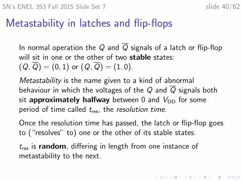
Metastability in latches and flip-flops
In normal operation the Q and Q signals of a latch or flip-flopwill sit in one or the other of two stable states:(Q,Q) = (0, 1) or (Q,Q) = (1, 0).
Metastability is the name given to a kind of abnormalbehaviour in which the voltages of the Q and Q signals bothsit approximately halfway between 0 and VDD for someperiod of time called tres, the resolution time.
Once the resolution time has passed, the latch or flip-flop goesto (“resolves” to) one or the other of its stable states.
tres is random, differing in length from one instance ofmetastability to the next.

SN’s ENEL 353 Fall 2015 Slide Set 7 slide 41/62
A mechanical analogy for metastability
There are two stable places for the ball: the bottom ofvalley 0, and the bottom of valley 1.
hill
valley 1valley 0
Given a gentle nudge, the ball will move a little, but stay invalley 0. Given a strong push, the ball will roll over the hill andsettle in valley 1.
What if the ball is given a push that gives it just enoughenergy to get to the top of the hill and stop?

SN’s ENEL 353 Fall 2015 Slide Set 7 slide 42/62
Why is metastability dangerous?
The key problem is this: tres will sometimes be much longerthan tpcq. Sometimes tres may be as long as one whole clockperiod in a synchronous system.
Of course, the output signal of a flip-flop or latch is typicallyan input signal to one or more other circuit elements.
A circuit element with a metastable input will probablygenerate an incorrect output.
So metastability in a single DFF could cause an entiresynchronous circuit to behave incorrectly, possibly getting thecircuit into a state from which it can’t recover.

SN’s ENEL 353 Fall 2015 Slide Set 7 slide 43/62
Preventing metastability from causing circuit
failure
A single DFF going metastable for a fraction of a clock cyclemay cause a synchronous system to behave incorrectly for amuch longer time period, and may even cause the system tofreeze completely.
One essential step inreducing the risk ofproblems is, as we’ve justseen, careful timing analysisof paths like this . . .
CL
CLK
But what about system inputs? Edges on inputs can havecompletely unpredictable timing relative to edges on thesystem clock!

SN’s ENEL 353 Fall 2015 Slide Set 7 slide 44/62
Examples of asynchronous inputs
In each of the systems below, A is what is called anasynchronous input . . .
button
A synchronous
system
CLK
A
CLK1
system 1
CLK2
system 2
synchro-nous
synchro-nous
CLK1 and CLK2 areunrelated, with differentfrequencies.
On the left, the system can’t control when a human mightpress or release the button. On the right, there will be nopredictable relationship between edges on A and edgeson CLK2.

SN’s ENEL 353 Fall 2015 Slide Set 7 slide 45/62
An example FSM with an asynchronous input
If we don’t know anything at all about when edges on A mightappear relative to edges on CLK, this is a bad design . . .
nextstatelogic
outputlogic Y
A
CLK
Why is it impossible to design the next state logic to preventdisastrous metastability in the state register?
To greatly reduce the risk, A can be passed though asynchronizer circuit, as shown on the next slide . . .
slide 46/62
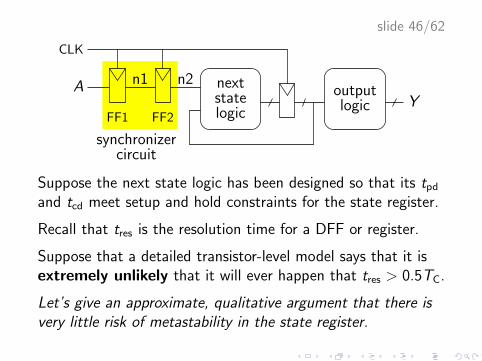
nextstatelogic
outputlogic Y
n2n1A
FF2FF1
synchronizercircuit
CLK
Suppose the next state logic has been designed so that its tpdand tcd meet setup and hold constraints for the state register.
Recall that tres is the resolution time for a DFF or register.
Suppose that a detailed transistor-level model says that it isextremely unlikely that it will ever happen that tres > 0.5TC.
Let’s give an approximate, qualitative argument that there isvery little risk of metastability in the state register.
SN’s ENEL 353 Fall 2015 Slide Set 7 slide 47/62
Detailed analysis of tres and synchronizers
In Sections 3.4.4–3.4.6, Harris and Harris present a formula forthe probability distribution of tres:
P(tres > t) =T0
TCexp
(−t
τ
)They go on to use that probability distribution to derive aformula for MTBF (mean time between failures) ofsynchronizer circuits.
In ENEL 353 in Fall 2015, we are not going to cover thatmaterial, and you will not be tested on it on the final exam.
You are expected to understand the qualitative ideas aboutmetastability and synchronizers presented in Sections 3.4.4and 3.4.5.
SN’s ENEL 353 Fall 2015 Slide Set 7 slide 48/62
Outline of Slide Set 7
Introduction to timing of sequential logic
Timing parameters for DFFs
Timing constraints for synchronous sequential logic
Clock skew
Clock skew, setup and hold time constraints
Violations of setup-and-hold-time rules, and metastability
Some insight into circuits, setup times, and metastability

SN’s ENEL 353 Fall 2015 Slide Set 7 slide 49/62
Some insight into circuits, setup times, and
metastability
The rest of the slides in this slide set are not exam material inENEL 353 in Fall 2015.
They are intended to provide some insight into why latchesand flip-flops must have setup times, and why latches andflip-flops can go metastable.
SN’s ENEL 353 Fall 2015 Slide Set 7 slide 50/62
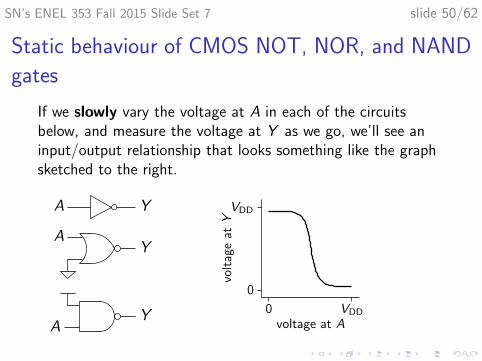
Static behaviour of CMOS NOT, NOR, and NAND
gates
If we slowly vary the voltage at A in each of the circuitsbelow, and measure the voltage at Y as we go, we’ll see aninput/output relationship that looks something like the graphsketched to the right.
A Y
A
AY
Y VDD
voltage at A
volt
age
atY
VDD
0
0
SN’s ENEL 353 Fall 2015 Slide Set 7 slide 51/62
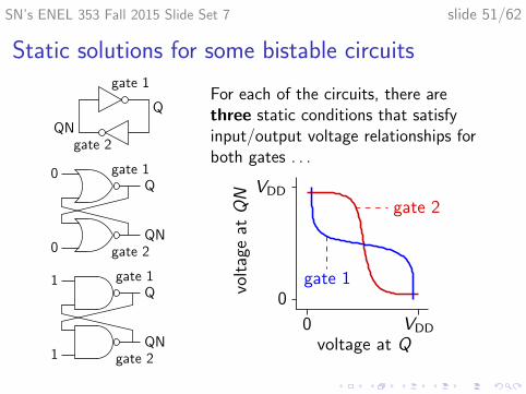
Static solutions for some bistable circuits
0
0
gate 1
1
1
gate 1
gate 2
gate 2
gate 1
Q
Q
QN
Q
QN
QN
gate 2
For each of the circuits, there arethree static conditions that satisfyinput/output voltage relationships forboth gates . . .
gate 2
gate 1
VDD
voltage at Q
VDD
0
0
volt
age
atQN
SN’s ENEL 353 Fall 2015 Slide Set 7 slide 52/62
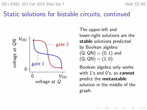
Static solutions for bistable circuits, continued
gate 2
gate 1
VDD
voltage at Q
VDD
0
0
volt
age
atQN
The upper-left andlower-right solutions are thestable solutions predictedby Boolean algebra:(Q,QN) = (0, 1) and(Q,QN) = (1, 0).
Boolean algebra only workswith 1’s and 0’s, so cannotpredict the metastablesolution in the middle of thegraph.

SN’s ENEL 353 Fall 2015 Slide Set 7 slide 53/62
Dynamic behaviour of bistable circuitsStatic analysis shows us only what the possible solutions arewhen dV /dt = 0 for both gate outputs, and does not tell ushow voltages might change as a function of time.
Transistor physics and circuit theory, beyond what has beentaught to year 2 ENEL and ENSF students, says . . .
I The static solutions that are identified by Boolean algebraare stable equilibrium points. If a bistable circuit is inone of its stable states, moderate amounts of electricalnoise will not move the state very far away from thatstable state.
I The metastable state of a bistable circuit is an unstableequilibrium point. A very tiny amount of electricalnoise will rapidly drive the circuit from there to one or theother of its stable equilibrium points.
SN’s ENEL 353 Fall 2015 Slide Set 7 slide 54/62
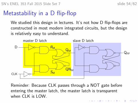
Metastability in a D flip-flop
We studied this design in lectures. It’s not how D flip-flops areconstructed in most modern integrated circuits, but the designis relatively easy to understand.
master D latch slave D latch
RM
SMCLK
DQM
QNM
QFF
Reminder: Because CLK passes through a NOT gate beforeentering the master latch, the master latch is transparentwhen CLK is LOW.

SN’s ENEL 353 Fall 2015 Slide Set 7 slide 55/62
Let’s look at what happens in the master latch when there isan edge on D just before a rising edge on CLK.
RM
SMCLK
DQM
QNM
CLK
SM
RM
D
In an ideal SR latch, (QM,QNM) will go to (1, 0) because ofthe pulse on SM. But in a real SR latch, the width of thepulse matters.
A wide pulse will make the latch “do the right thing.”
A very narrow pulse will not decrease the voltage at QNM
very much, and the voltage at QM won’t change at all.(QM,QNM) will settle back to (0, 1).
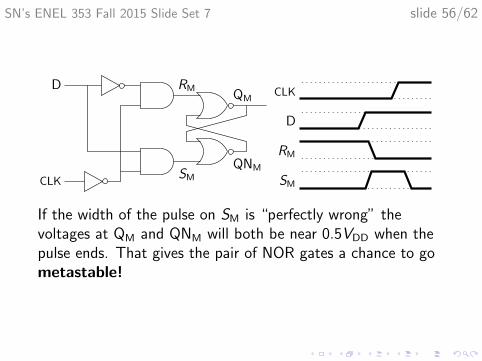
SN’s ENEL 353 Fall 2015 Slide Set 7 slide 56/62
RM
SMCLK
DQM
QNM
CLK
SM
RM
D
If the width of the pulse on SM is “perfectly wrong” thevoltages at QM and QNM will both be near 0.5VDD when thepulse ends. That gives the pair of NOR gates a chance to gometastable!
SN’s ENEL 353 Fall 2015 Slide Set 7 slide 57/62
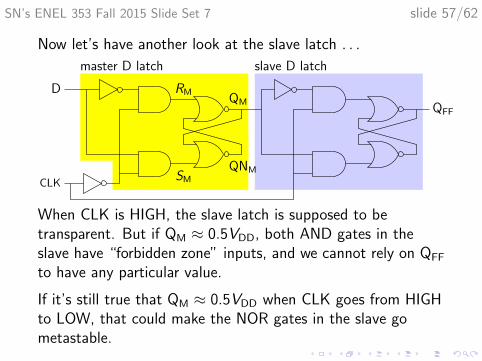
Now let’s have another look at the slave latch . . .
master D latch slave D latch
RM
SMCLK
DQM
QNM
QFF
When CLK is HIGH, the slave latch is supposed to betransparent. But if QM ≈ 0.5VDD, both AND gates in theslave have “forbidden zone” inputs, and we cannot rely on QFF
to have any particular value.
If it’s still true that QM ≈ 0.5VDD when CLK goes from HIGHto LOW, that could make the NOR gates in the slave gometastable.

SN’s ENEL 353 Fall 2015 Slide Set 7 slide 58/62
Setup time in a modern DFF
Below is a D latch suitable for use as the master latch in aDFF. Switches S1 and S2 are implemented in CMOS usingsimple two-transistor devices called transmission gates.
QM
CLK
D
CLK
S1
QNMCLK
CLK
S2
I1 I2
I3
n1
CLK S1 S2 latch conditionLOW closed open transparentHIGH open closed opaque
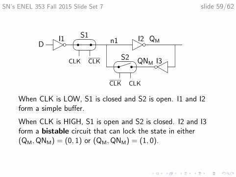
SN’s ENEL 353 Fall 2015 Slide Set 7 slide 59/62
QM
CLK
D
CLK
S1
QNMCLK
CLK
S2
I1 I2
I3
n1
When CLK is LOW, S1 is closed and S2 is open. I1 and I2form a simple buffer.
When CLK is HIGH, S1 is open and S2 is closed. I2 and I3form a bistable circuit that can lock the state in either(QM,QNM) = (0, 1) or (QM,QNM) = (1, 0).
SN’s ENEL 353 Fall 2015 Slide Set 7 slide 60/62
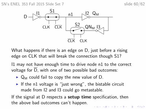
QM
CLK
D
CLK
S1
QNMCLK
CLK
S2
I1 I2
I3
n1
What happens if there is an edge on D, just before a risingedge on CLK that will break the connection though S1?
I1 may not have enough time to drive node n1 to the correctvoltage for D, with one of two possible bad outcomes:
I QM could fail to copy the new value of D.
I If the n1 voltage is “just wrong”, the bistable circuitmade from I2 and I3 could go metastable.
If the signal at D respects a setup time specification, thenthe above bad outcomes can’t happen.
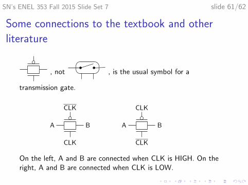
SN’s ENEL 353 Fall 2015 Slide Set 7 slide 61/62
Some connections to the textbook and other
literature
, not , is the usual symbol for a
transmission gate.
CLK
A B
CLK
CLK
BA
CLK
On the left, A and B are connected when CLK is HIGH. On theright, A and B are connected when CLK is LOW.

SN’s ENEL 353 Fall 2015 Slide Set 7 slide 62/62
More connections to the textbook and other
literature
Here is the complete DFF design. Note that the invertingtristate buffers T1 and T2 are really just inverters followed bytransmission gates.
CLK
DN1
CLK
CLK
CLK
I1 I2
T1
I3
CLK
CLK
T2
CLK
CLK
I4 QN2
Image is Figure 3.13 from Harris D. M. and Harris S. L., Digital Designand Computer Architecture, 2nd ed., c© 2013, Elsevier, Inc.