Embed Size (px)
Citation preview

WELSH JOINT EDUCATION COMMITTEE CYD-BWYLLGOR ADDYSG CYMRU
General Certificate of Secondary Education Tystysgrif Gyffredinol Addysg Uwchradd
ELECTRONICS
TERMINAL EXAMINATION
HIGHER TIER
A.M. TUESDAY, 24 June 2003
(75 minutes)
VP*(0298/2)
298/02
Centre Number
Candidate’s Name (in full)
Candidate’s Examination Number
For Examiner’suse only.
1
2
3
4
5
6
7
8
9
10
Total
INSTRUCTIONS TO CANDIDATES
Write your centre number, name and candidate number in the spaces provided above.
Answer all questions.
Write all the answers in the spaces provided in this booklet.
INFORMATION FOR CANDIDATES
The number of marks is given in brackets at the end of each question or part-question.
No certificate will be awarded to a candidate detected in any unfair practice during theexamination.

2
INFORMATION SHEET
This information may be of use in answering the questions.
1. Resistor ColourCodes
BLACK 0
BROWN 1
RED 2
ORANGE 3
YELLOW 4
GREEN 5
BLUE 6
VIOLET 7
GREY 8
WHITE 9
The fourth bandcolour gives thetolerance as follows:GOLD ± 5%SILVER ± 10%
2. Preferred Values for Resistors
E 12 SERIES OF PREFERRED VALUES10; 12; 15; 18; 22; 27; 33; 39; 47; 56; 68; 82 and multiples thereafter
3. Resistance =
4. Effective resistance, R, of two resistors R1
and R2
in series is given by R = R1
+ R2.
5. Effective resistance, R, of two resistors R1
and R2
in parallel is given by
6. Voltage Divider
voltagecurrent
; R = VI
7. Power = voltage ¥ current;
8. LED The forward voltage drop across a LED is 2V.
9. Transistors
(i) Current gain =
(ii) The forward voltage drop across the base emitter junction is 0·7V.
R R RR R
1
1= +
2
2
P VI I R VR
2
= = =2 .
Collector currentBase current
h IIFE
C
B; =
+VS
0V
R1
R2 V R
R R VOUT 2
1 2S= ¥
+
.
.
.
(0298/2)
3 Examineronly
Arholwryn unig
Answer all questions in the spaces provided.
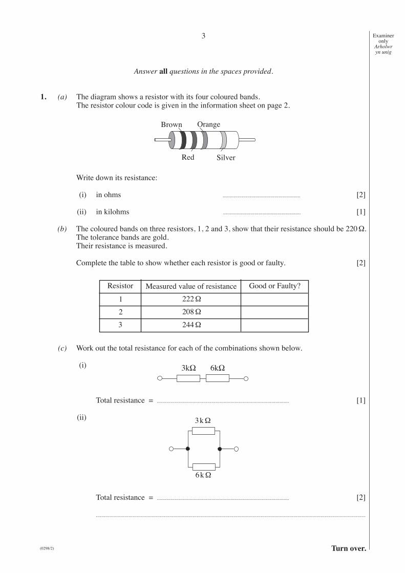
1. (a) The diagram shows a resistor with its four coloured bands.The resistor colour code is given in the information sheet on page 2.
(0298/2)
Brown Orange
Red Silver
Write down its resistance:
(i) in ohms . . . . . . . . . . . . . . . . . . . . . . . . . . . . . . . . . . . . . . . . . . . . . . . . . . . . . . . . . [2]
(ii) in kilohms . . . . . . . . . . . . . . . . . . . . . . . . . . . . . . . . . . . . . . . . . . . . . . . . . . . . . . . . . [1]
(b) The coloured bands on three resistors, 1, 2 and 3, show that their resistance should be 220Ω.The tolerance bands are gold.Their resistance is measured.
Complete the table to show whether each resistor is good or faulty. [2]
Resistor
1
2
3
Measured value of resistance
222Ω
208Ω
244Ω
Good or Faulty?
(c) Work out the total resistance for each of the combinations shown below.
(i) 3kW 6kW
Total resistance = . . . . . . . . . . . . . . . . . . . . . . . . . . . . . . . . . . . . . . . . . . . . . . . . . . . . . . . . . . . . . . . . . . . . . . . . . . . . . . . . . . . . . . . . . . . . . . . . . [1]
(ii) 3kΩ
6kΩ
Total resistance = . . . . . . . . . . . . . . . . . . . . . . . . . . . . . . . . . . . . . . . . . . . . . . . . . . . . . . . . . . . . . . . . . . . . . . . . . . . . . . . . . . . . . . . . . . . . . . . . . [2]
. . . . . . . . . . . . . . . . . . . . . . . . . . . . . . . . . . . . . . . . . . . . . . . . . . . . . . . . . . . . . . . . . . . . . . . . . . . . . . . . . . . . . . . . . . . . . . . . . . . . . . . . . . . . . . . . . . . . . . . . . . . . . . . . . . . . . . . . . . . . . . . . . . . . . . . . . . . . . . . . . . . . . . . . . . . . . . . . . . . . . . . . . . . . . . . . . . . . . .
Turn over.

4 Examineronly
Arholwryn unig
2. The block diagram for a burglar alarm is shown below.
(0298/2)
Lightsensing
unit
Pressuresensing
unit
X Latch
Resetswitch
BuzzerTransducerdriver
The burglar alarm has two sensors:1. a light-sensing unit which sets the alarm automatically only at night,2. a pressure switch, under the door mat.
(a) The light sensing unit outputs logic 0 in darkness, and logic 1 in daylight.The pressure sensing unit outputs logic 0 when pressed, and logic 1 when released.
X is a logic gate.It must output a logic 1 only when someone stands on the doormat when it is night-time.
(i) Complete the truth table. [1]
Light sensing unit
0
0
1
1
Pressure sensing unit Output of X
0
1
0
1
(ii) What logic gate must be used in sub-system X? . . . . . . . . . . . . . . . . . . . . . . . . . . . . . . . . . . . . . . . . . . . . . . . . . . . . . . . . . [1]
(b) Part of the latch circuit is shown below.Draw the four connections needed to make the latch set and reset. [4]
5V
Signal fromsub-system
X
D Q
R
0V
Resetswitch
Output oflatch

5 Examineronly
Arholwryn unig
3. (a) Here are the symbols for five types of logic gates, labelled A, B, C, D and E:
(0298/2)
A B C D E
(i) Which is the symbol for an OR gate? . . . . . . . . . . . . . . . . . . . . . . . . . . . . . . . . . . . . . . . . . . . . . . . . . . . . . . . . . [1]
(ii) Which of these logic gates gives the opposite behaviour to an OR gate?
. . . . . . . . . . . . . . . . . . . . . . . . . . . . . . . . . . . . . . . . . . . . . . . . . . . . . . . . . [1]
(iii) Which of these logic gates gives an output of logic 1 only when both inputs are at
logic 1? . . . . . . . . . . . . . . . . . . . . . . . . . . . . . . . . . . . . . . . . . . . . . . . . . . . . . . . . . [1]
(b) A
BP
Q
Complete the truth table for the logic system shown above. [2]
A
0
0
1
1
B
0
1
0
1
P Q
(c) (i) Redraw the system replacing the logic gates with their NAND gate equivalents. [2]
(ii) Draw a line through any redundant gates. [1]
Turn over.

6 Examineronly
Arholwryn unig
4. The following diagram shows a resistor-capacitor network.
(0298/2)
9V
0V
Before the switch is closed, the capacitor is not charged.
(a) Which of the following statements is true?After the switch is closed
A. the voltage VC decreases.B. the voltage VC stays the same.C. the voltage VC increases.
Answer . . . . . . . . . . . . . . . . . . . . . . . . . . . [1]
(b) This circuit can be used to produce a time delay in a monostable circuitWhich of the following combinations of resistor and capacitor will produce the biggest timedelay?
A. R = 10kΩ C = 1 mFB. R = 10kΩ C = 10 mFC. R = 1kΩ C = 1 mFD. R = 1kΩ C = 10 mF
Answer . . . . . . . . . . . . . . . . . . . . . . . . . . . [1]
(c) Here is the circuit diagram for a monostable, used in an egg timer.
0V
9V
330mF
4 8
3
7
6
555
1
2Input Output
R
C VC

7 Examineronly
Arholwryn unig
(0298/2)
The variable resistor has a maximum resistance of 1MΩ.Use the formula:
T = 1·1RC
to calculate the maximum cooking time for the egg, in seconds. [2]
. . . . . . . . . . . . . . . . . . . . . . . . . . . . . . . . . . . . . . . . . . . . . . . . . . . . . . . . . . . . . . . . . . . . . . . . . . . . . . . . . . . . . . . . . . . . . . . . . . . . . . . . . . . . . . . . . . . . . . . . . . . . . . . . . . . . . . . . . . . . . . . . . . . . . . . . . . . . . . . . . . . . . . . . . . . . . . . . . . . . . . . . . . . . . . . . . . . . . . . . . . . . . . . . . . . . . . . . . . . . . . . . . . . .
. . . . . . . . . . . . . . . . . . . . . . . . . . . . . . . . . . . . . . . . . . . . . . . . . . . . . . . . . . . . . . . . . . . . . . . . . . . . . . . . . . . . . . . . . . . . . . . . . . . . . . . . . . . . . . . . . . . . . . . . . . . . . . . . . . . . . . . . . . . . . . . . . . . . . . . . . . . . . . . . . . . . . . . . . . . . . . . . . . . . . . . . . . . . . . . . . . . . . . . . . . . . . . . . . . . . . . . . . . . . . . . . . . . .
. . . . . . . . . . . . . . . . . . . . . . . . . . . . . . . . . . . . . . . . . . . . . . . . . . . . . . . . . . . . . . . . . . . . . . . . . . . . . . . . . . . . . . . . . . . . . . . . . . . . . . . . . . . . . . . . . . . . . . . . . . . . . . . . . . . . . . . . . . . . . . . . . . . . . . . . . . . . . . . . . . . . . . . . . . . . . . . . . . . . . . . . . . . . . . . . . . . . . . . . . . . . . . . . . . . . . . . . . . . . . . . . . . . .
. . . . . . . . . . . . . . . . . . . . . . . . . . . . . . . . . . . . . . . . . . . . . . . . . . . . . . . . . . . . . . . . . . . . . . . . . . . . . . . . . . . . . . . . . . . . . . . . . . . . . . . . . . . . . . . . . . . . . . . . . . . . . . . . . . . . . . . . . . . . . . . . . . . . . . . . . . . . . . . . . . . . . . . . . . . . . . . . . . . . . . . . . . . . . . . . . . . . . . . . . . . . . . . . . . . . . . . . . . . . . . . . . . . .
Turn over.

8 Examineronly
Arholwryn unig
5. A transistor is used to switch on a 100mA buzzer when the light level gets too bright.The circuit diagram for this system is shown below.
(0298/2)
6V
6V 100mABuzzer
0V
V1
V3
V2
(a) The table gives information about four transistors.
Which transistor A,B,C, or D will drive the buzzer correctly and draw the smallest possiblecurrent from the light sensing unit?
(i) Answer . . . . . . . . . . . . . . . . . . . . . . . . . . . . . . . . . . . . . . . . . . . . . . . . . . . . . . . . . [2]
(ii) For your chosen transistor in (i), calculate the base current when the collectorcurrent is 100mA. [1]
. . . . . . . . . . . . . . . . . . . . . . . . . . . . . . . . . . . . . . . . . . . . . . . . . . . . . . . . . . . . . . . . . . . . . . . . . . . . . . . . . . . . . . . . . . . . . . . . . . . . . . . . . . . . . . . . . . . . . . . . . . . . . . . . . . . . . . . . . . . . . . . . . . . . . . . . . . . . . . . . . . . . . . . . . . . . . . . . . . . . . . . . . . . . . . . . . . . . . .
. . . . . . . . . . . . . . . . . . . . . . . . . . . . . . . . . . . . . . . . . . . . . . . . . . . . . . . . . . . . . . . . . . . . . . . . . . . . . . . . . . . . . . . . . . . . . . . . . . . . . . . . . . . . . . . . . . . . . . . . . . . . . . . . . . . . . . . . . . . . . . . . . . . . . . . . . . . . . . . . . . . . . . . . . . . . . . . . . . . . . . . . . . . . . . . . . . . . . .
. . . . . . . . . . . . . . . . . . . . . . . . . . . . . . . . . . . . . . . . . . . . . . . . . . . . . . . . . . . . . . . . . . . . . . . . . . . . . . . . . . . . . . . . . . . . . . . . . . . . . . . . . . . . . . . . . . . . . . . . . . . . . . . . . . . . . . . . . . . . . . . . . . . . . . . . . . . . . . . . . . . . . . . . . . . . . . . . . . . . . . . . . . . . . . . . . . . . . .
Transistor
A
B
C
TO18
E-line
TO39
TO5
100
200
50
40
300mA
50mA
800mA
1·2AD
PackageCurrent gain
hFE
MaximumCurrent

9 Examineronly
Arholwryn unig
(0298/2)
(b) The transistor is switched on (saturated). Find the value of
(i) the voltage V1, . . . . . . . . . . . . . . . . . . . . . . . . . . . . . . . . . . . . . . . . . . . . . . . . . . . . . . . . . [1]
(ii) the voltage V2, . . . . . . . . . . . . . . . . . . . . . . . . . . . . . . . . . . . . . . . . . . . . . . . . . . . . . . . . . [1]
(iii) the voltage V3, . . . . . . . . . . . . . . . . . . . . . . . . . . . . . . . . . . . . . . . . . . . . . . . . . . . . . . . . . [1]
(iv) the power dissipated in the buzzer, [2]
. . . . . . . . . . . . . . . . . . . . . . . . . . . . . . . . . . . . . . . . . . . . . . . . . . . . . . . . . . . . . . . . . . . . . . . . . . . . . . . . . . . . . . . . . . . . . . . . . . . . . . . . . . . . . . . . . . . . . . . . . . . . . . . . . . . . . . . . . . . . . . . . . . . . . . . . . . . . . . . . . . . . . . . . . . . . . . . . . . . . . . . . . . . . . . . . . . . . . .
. . . . . . . . . . . . . . . . . . . . . . . . . . . . . . . . . . . . . . . . . . . . . . . . . . . . . . . . . . . . . . . . . . . . . . . . . . . . . . . . . . . . . . . . . . . . . . . . . . . . . . . . . . . . . . . . . . . . . . . . . . . . . . . . . . . . . . . . . . . . . . . . . . . . . . . . . . . . . . . . . . . . . . . . . . . . . . . . . . . . . . . . . . . . . . . . . . . . . .
(v) the power dissipated in the transistor. [1]
. . . . . . . . . . . . . . . . . . . . . . . . . . . . . . . . . . . . . . . . . . . . . . . . . . . . . . . . . . . . . . . . . . . . . . . . . . . . . . . . . . . . . . . . . . . . . . . . . . . . . . . . . . . . . . . . . . . . . . . . . . . . . . . . . . . . . . . . . . . . . . . . . . . . . . . . . . . . . . . . . . . . . . . . . . . . . . . . . . . . . . . . . . . . . . . . . . . . . .
. . . . . . . . . . . . . . . . . . . . . . . . . . . . . . . . . . . . . . . . . . . . . . . . . . . . . . . . . . . . . . . . . . . . . . . . . . . . . . . . . . . . . . . . . . . . . . . . . . . . . . . . . . . . . . . . . . . . . . . . . . . . . . . . . . . . . . . . . . . . . . . . . . . . . . . . . . . . . . . . . . . . . . . . . . . . . . . . . . . . . . . . . . . . . . . . . . . . . .
Turn over.

10 Examineronly
Arholwryn unig
(0298/2)
6. The block diagram for PA (public address) amplifier system is shown below.
Microphone . . . . . . . . . . . . . . . . . . . . . . . . . . . . . . . . . . . . .
. . . . . . . . . . . . . . . . . . . . . . . . . . . . . . . . . . . . .
. . . . . . . . . . . . . . . . . . . . . . . . . . . . . . . . . . . . .
. . . . . . . . . . . . . . . . . . . . . . . . . . . . . . . . . . . . .
. . . . . . . . . . . . . . . . . . . . . . . . . . . . . . . . . . . . .
. . . . . . . . . . . . . . . . . . . . . . . . . . . . . . . . . . . . .
. . . . . . . . . . . . . . . . . . . . . . . . . . . . . . . . . . . . .
. . . . . . . . . . . . . . . . . . . . . . . . . . . . . . . . . . . . .
Microphone
Loudspeaker
(a) (i) Identify the unnamed blocks, using sub-systems from the following list.Write your answers on the dotted lines provided. [3]
preamplifier voltage divider power amplifier
comparator Schmitt trigger mixer
Hint: One of these sub-systems is used twice.
(ii) How does the job of the preamplifier differ from that of the power amplifier? [2]
. . . . . . . . . . . . . . . . . . . . . . . . . . . . . . . . . . . . . . . . . . . . . . . . . . . . . . . . . . . . . . . . . . . . . . . . . . . . . . . . . . . . . . . . . . . . . . . . . . . . . . . . . . . . . . . . . . . . . . . . . . . . . . . . . . . . . . . . . . . . . . . . . . . . . . . . . . . . . . . . . . . . . . . . . . . . . . . . . . . . . . . . . . . . . . . . . . . . . .
. . . . . . . . . . . . . . . . . . . . . . . . . . . . . . . . . . . . . . . . . . . . . . . . . . . . . . . . . . . . . . . . . . . . . . . . . . . . . . . . . . . . . . . . . . . . . . . . . . . . . . . . . . . . . . . . . . . . . . . . . . . . . . . . . . . . . . . . . . . . . . . . . . . . . . . . . . . . . . . . . . . . . . . . . . . . . . . . . . . . . . . . . . . . . . . . . . . . . .
. . . . . . . . . . . . . . . . . . . . . . . . . . . . . . . . . . . . . . . . . . . . . . . . . . . . . . . . . . . . . . . . . . . . . . . . . . . . . . . . . . . . . . . . . . . . . . . . . . . . . . . . . . . . . . . . . . . . . . . . . . . . . . . . . . . . . . . . . . . . . . . . . . . . . . . . . . . . . . . . . . . . . . . . . . . . . . . . . . . . . . . . . . . . . . . . . . . . . .
(b) Here are four possible bandwidth choices for this PA amplifier system.
A. 100Hz to 12kHz
B. 12Hz to 50kHz
C. 50Hz to 100kHz
D. 100Hz to 1MHz
(i) Which is the best choice for this amplifier system? . . . . . . . . . . . . . . . . . . . . . . . . . . . . [1]
(ii) Give a reason for your answer to part (i) [1]
. . . . . . . . . . . . . . . . . . . . . . . . . . . . . . . . . . . . . . . . . . . . . . . . . . . . . . . . . . . . . . . . . . . . . . . . . . . . . . . . . . . . . . . . . . . . . . . . . . . . . . . . . . . . . . . . . . . . . . . . . . . . . . . . . . . . . . . . . . . . . . . . . . . . . . . . . . . . . . . . . . . . . . . . . . . . . . . . . . . . . . . . . . . . . . . . . . . . . .
. . . . . . . . . . . . . . . . . . . . . . . . . . . . . . . . . . . . . . . . . . . . . . . . . . . . . . . . . . . . . . . . . . . . . . . . . . . . . . . . . . . . . . . . . . . . . . . . . . . . . . . . . . . . . . . . . . . . . . . . . . . . . . . . . . . . . . . . . . . . . . . . . . . . . . . . . . . . . . . . . . . . . . . . . . . . . . . . . . . . . . . . . . . . . . . . . . . . . .
. . . . . . . . . . . . . . . . . . . . . . . . . . . . . . . . . . . . . . . . . . . . . . . . . . . . . . . . . . . . . . . . . . . . . . . . . . . . . . . . . . . . . . . . . . . . . . . . . . . . . . . . . . . . . . . . . . . . . . . . . . . . . . . . . . . . . . . . . . . . . . . . . . . . . . . . . . . . . . . . . . . . . . . . . . . . . . . . . . . . . . . . . . . . . . . . . . . . . .
. . . . . . . . . . . . . . . . . . . . . . . . . . . . . . . . . . . . . . . . . . . . . . . . . . . . . . . . . . . . . . . . . . . . . . . . . . . . . . . . . . . . . . . . . . . . . . . . . . . . . . . . . . . . . . . . . . . . . . . . . . . . . . . . . . . . . . . . . . . . . . . . . . . . . . . . . . . . . . . . . . . . . . . . . . . . . . . . . . . . . . . . . . . . . . . . . . . . . .

11 Examineronly
Arholwryn unig
(0298/2)
7. (a) Draw the circuit diagram for a non-inverting amplifier, which makes use of an op-amp andtwo resistors. [3]
+
_
(b) Calculate suitable values for the resistors so that the amplifier has a voltage gain of 40.Label the resistors, on your circuit diagram, with the values you have chosen. [2]
. . . . . . . . . . . . . . . . . . . . . . . . . . . . . . . . . . . . . . . . . . . . . . . . . . . . . . . . . . . . . . . . . . . . . . . . . . . . . . . . . . . . . . . . . . . . . . . . . . . . . . . . . . . . . . . . . . . . . . . . . . . . . . . . . . . . . . . . . . . . . . . . . . . . . . . . . . . . . . . . . . . . . . . . . . . . . . . . . . . . . . . . . . . . . . . . . . . . . . . . . . . . . . . . . . . .
. . . . . . . . . . . . . . . . . . . . . . . . . . . . . . . . . . . . . . . . . . . . . . . . . . . . . . . . . . . . . . . . . . . . . . . . . . . . . . . . . . . . . . . . . . . . . . . . . . . . . . . . . . . . . . . . . . . . . . . . . . . . . . . . . . . . . . . . . . . . . . . . . . . . . . . . . . . . . . . . . . . . . . . . . . . . . . . . . . . . . . . . . . . . . . . . . . . . . . . . . . . . . . . . . . . .
. . . . . . . . . . . . . . . . . . . . . . . . . . . . . . . . . . . . . . . . . . . . . . . . . . . . . . . . . . . . . . . . . . . . . . . . . . . . . . . . . . . . . . . . . . . . . . . . . . . . . . . . . . . . . . . . . . . . . . . . . . . . . . . . . . . . . . . . . . . . . . . . . . . . . . . . . . . . . . . . . . . . . . . . . . . . . . . . . . . . . . . . . . . . . . . . . . . . . . . . . . . . . . . . . . . .
. . . . . . . . . . . . . . . . . . . . . . . . . . . . . . . . . . . . . . . . . . . . . . . . . . . . . . . . . . . . . . . . . . . . . . . . . . . . . . . . . . . . . . . . . . . . . . . . . . . . . . . . . . . . . . . . . . . . . . . . . . . . . . . . . . . . . . . . . . . . . . . . . . . . . . . . . . . . . . . . . . . . . . . . . . . . . . . . . . . . . . . . . . . . . . . . . . . . . . . . . . . . . . . . . . . .
Turn over.

12 Examineronly
Arholwryn unig
(0298/2)
(c) The output of this amplifier saturates at ± 10V.A signal is applied to the input of the amplifier. This is shown in the diagram below.Draw the output signal produced by the amplifier, using the axes provided. [2]
0
10
20
–10
–20
Voltage/mV
Input Time
0
200
400
–200
–400
600
–600
Voltage/mV
Output Time

13 Examineronly
Arholwryn unig
(0298/2)
8. The block diagram for a simple radio receiver is shown below.
A
B C D
(a) Identify the sub-systems labelled A, B, C and D. [3]Choose your answers from the following list:
demodulator aerial headphones tuned circuit
Sub-system A = . . . . . . . . . . . . . . . . . . . . . . . . . . . . . . . . . . . . . . . . . . . . . . . . . . . . . . . . .
Sub-system B = . . . . . . . . . . . . . . . . . . . . . . . . . . . . . . . . . . . . . . . . . . . . . . . . . . . . . . . . .
Sub-system C = . . . . . . . . . . . . . . . . . . . . . . . . . . . . . . . . . . . . . . . . . . . . . . . . . . . . . . . . .
Sub-system D = . . . . . . . . . . . . . . . . . . . . . . . . . . . . . . . . . . . . . . . . . . . . . . . . . . . . . . . . .
(b) Which sub-system:
(i) picks up the radio waves from free space: . . . . . . . . . . . . . . . . . . . . . . . . . . . . . . . . . . . . . . . . . . . . . . . . . . . . . . . . . . [1]
(ii) selects the desired radio station; . . . . . . . . . . . . . . . . . . . . . . . . . . . . . . . . . . . . . . . . . . . . . . . . . . . . . . . . . . [1]
(iii) is the output device; . . . . . . . . . . . . . . . . . . . . . . . . . . . . . . . . . . . . . . . . . . . . . . . . . . . . . . . . . . [1]
(iv) contains a diode; . . . . . . . . . . . . . . . . . . . . . . . . . . . . . . . . . . . . . . . . . . . . . . . . . . . . . . . . . . [1]
(v) contains a variable capacitor . . . . . . . . . . . . . . . . . . . . . . . . . . . . . . . . . . . . . . . . . . . . . . . . . . . . . . . . . [1]
(c) What is the name of the component in this radio receiver that allows current to flow throughit in one direction only? [1]
. . . . . . . . . . . . . . . . . . . . . . . . . . . . . . . . . . . . . . . . . . . . . . . . . . . . . . . . . . . . . . . . . . . . . . . . . . . . . . . . . . . . . . . . . . . . . . . . . . . . . . . . . . . . . . . . . . . . . . . . . . . . . . . . . . . . . . . . . . . . . . . . . . . . . . . . . . . . . . . . . . . . . . . . . . . . . . . . . . . . . . . . . . . . . . . . . . . . . . . . . . . . . . . . . . . .
Turn over.

14 Examineronly
Arholwryn unig
(0298/2)
9. Two processes are needed to digitise an analogue signal.The signal must first be sampled to produce a PAM (pulse amplitude modulated) signal.The PAM signal is then converted to a binary number by an ADC.
(a) What does the abbreviation ADC stand for?
. . . . . . . . . . . . . . . . . . . . . . . . . . . . . . . . . . . . . . . . . . . . . . . . . . . . . . . . . . . . . . . . . . . . . . . . . . . . . . . . . . . . . . . . . . . . . . . . . . . . . . . . . . . . . . . . . . . . . . . . . . . . . . . . . . . . . . . . . . [1]
(b) The graph shows an analogue signal, which is being sampled at the times shown.
Voltage / V
Firstsamplingpulse
Secondsamplingpulse
Thirdsamplingpulse
Complete the table to show the voltages of the PAM signal. [2]
Sampling pulse
First
Second
Third
PAM voltage
(c) The PAM signal is then processed by the ADC.The next table shows the binary output for various values of PAM voltage.Some rows have already been completed. Use this information to complete the rest. [2]
PAM voltage
0·1V
0·2V
0·3V
0·4V
1·0V
ADC binary output
0001
0010
0011
Time0
0.4
0.8
1.2

10. Passengers travelling on an underground railway in a big city use a lift to travel between streetlevel and the railway platform, below ground.
Part of the lift control system counts the number of people entering the lift. When 10 people haveentered the lift, it switches on a ‘Lift Full’ sign. The remainder of the control program then takesover.
Draw a flowchart for the first part of the control system, using the following instructions: [7]
Instructions: Does the counter = 10?Has someone entered?
Reset the counterSwitch on the ‘Lift Full’ sign
Add 1 to the counter
15 Examineronly
Arholwryn unig
(0298/2)
Start
No
Yes
Rest of programme
. . . . . . . . . . . . . . . . . . . . . . . . . . . . . . . . . . . . . . . . . . . . . . . . . . . . . . . . . . . . . . . . . . . . . . . . . . . . . . . . . . . . . . . . . . . . . . . . . . . . . . . . . . . . . . . . . . . . . . . . . . . . . . . . . . . . . . . . . . . . . . . . . . . .
. . . . . . . . . . . . . . . . . . . . . . . . .
. . . . . . . . . . . . . . . . . . . . . . . . . . . . . . . . . . . . . . . . . . . . . . . . . . . . . . . . . . . . . . . . . . . . . . . . . . . . . . . . . . . . . . .
. . . . . . . . . . . . . . . . . . . . . . . . .