Embed Size (px)
Citation preview

【 ◆ 】 Finally Specification
CUSTOMER'S APPROVAL
SIGNATURE: DATE:
APPROVED PM PD PREPAREDBY REVIEWD REVIEWD BY
Wayne Li tong Zhengjinrong Jully
Prepared By :
FORMIKE ELECTRONIC CO.,LTDAddress : A909, Huaying Building, 97 Nanshang Road,Nanshan District, Shenzhen, China.518054TEL:(86) 755 88306921,88306931 FAX:(86) 755 88304615 Http:// www.wandisplay.com
● This specification is subject to change withouth notice.Please contact FORMIKE or it's representative before designing your product based on this specification.
1 Issued Date: Feb-25-2008
【 】 Preliminary Specification
FORMIKE ELECTRONIC CO.,LTD
PRDUCT SPECIFICATON
TFT LCD MODULEMODEL : KWH035ST12-F01

Revision Record
Data(y/m/d) Ver. Description Note page
2007.07.31 00 New
Formike Electronic Co.,Ltd ___________________________________________Model No.:KWH035ST12-F01
2

Contents
1. SPECIFICATIONS
1.1 Features
1.2 Mechanical Specifications
1.3 Absolute Maximum Ratings
1.4 DC Electrical Characteristics
1.5 Optical Characteristics
1.6 Backlight Characteristics
2. MODULE STRUCTURE
2.1 Counter Drawing
2.2 Interface Pin Description
2.3 Timing Characteristics
2.4 Power Sequence
2.4.1 Power up sequence
2.4.2 Power down sequence
2.5 Reference Initial code
3. QUALITY ASSURANCE SYSTEM
3.1 Quality Assurance Flow Chart
3.2 Inspection Specification
4. RELIABILITY TEST
4.1 Reliability Test Condition
5. PRECAUTION RELATING PRODUCT HANDLING
5.1 Safety
5.2 Handling
5.3 Storage
5.4 Terms of Warranty
Appendix: LCM Drawing
Packaging
Note: For detailed information please refer to IC data sheet:
Primacy (TFT LCD): Himax: HX8238-A
Formike Electronic Co.,LtdModel No.:KWH035ST12-F01 ___________________________________________
3

1. SPECIFICATIONS
1.1 Features
Main LCD panel
Item Standard Value
Display Type 320(R,G,B)*240 Dots
LCD Type Normally white, Transmissive type
Screen size(inch) 3.5inch
Viewing Direction 6 O’clock
Color configuration RGB-Strip
Backlight LED
Interface Digital 24-bits RGB
Other (controller/driver IC) Himax: HX8238-A
1.2 Mechanical Specifications
Item Standard Value Unit
Outline Dimension 76.9(W)*63.9(L)*3.5(H) (MAX) mm
LCD panel
Item Standard Value Unit
Viewing Area 72.88(W)*55.36(L) mm
Active Area 70.08(W)*52.56(L) mm
Note: For detailed information please refer to LCM drawing
Formike Electronic Co.,LtdModel No.:KWH035ST12-F01 ___________________________________________
4

1.3 Absolute Maximum Ratings
Module
Item Symbol Condition Min. Max. Unit
System Power Supply Voltage VDDIO VSS=0 -0.3 4.0 V
Input Voltage Vi - -0.3 5.0 V
Operating Temperature Top - -20 70 ℃
Storage Temperature TST - -30 80 ℃
1.4 DC Electrical Characteristics
Module VSS=0V, Ta=25℃
Item Symbol Condition Min. Typ. Max Unit
Power Supply Voltage1 VDDIO - 3.0 3.3 3.6 V
Vcom High Voltage VCOMH - 2.5 (3.6) 4.5 V
Vcom Low Voltage VCOML - -3 (-2.4) 0 V
Supply Current IDD VDD=3V
Pattern=black*1 - 5.5 8.5 mA
Note 1: Maximum Current display
Formike Electronic Co.,LtdModel No.:KWH035ST12-F01 ___________________________________________
5

1.5 Optical Characteristics
TFT LCD Module VDDIO=3.3V, Ta=25℃
Item Symbol Condition Min. Typ. Max. Unit -
Response time Tr+Tf Ta=25℃
θX,θY=0° - 50 70 ms Note2
Top Θy+ - 45 -
Bottom Θy- - 50 -
Left Θx- - 50 - Viewing angle
Right Θx+
CR 10
- 50 -
Deg Note4
Contrast ratio CR Ta=25℃
θX,θY=0° 200 250 - - Note3
X 0.259 0.309 0.359 White
Y 0.274 0.324 0.374
X 0.573 0.623 0.673 Red
Y 0.310 0.360 0.410
X 0.291 0.341 0.391 Green
Y 0.547 0.597 0.647
X 0.094 0.144 0.194
Color of CIE
Coordinate
(With B/L)
Blue Y
-
0.029 0.079 0.129
-
Average Brightness
Pattern=white display
(With LCD)
IV IF=20mA 220 250 - cd/m2
Uniformity
(With LCD)*1 △B IF=20mA 70 - - %
NoteA
Note A:
*1: △B=B (min) / B(max)
*2: Measurement Condition for Optical Characteristics:
a: Environment 25℃±5℃/60±20%R.H, no wind, dark room below 10 Lux at typical lamp
current and typical operating frequency.
b: Measurement Distance 500±50mm, (θ=0∘)
c: Equipment: TOPCON BM-7 fast, (field 1∘), after 10 minutes operation.
d: The uncertainty of the C.I.E coordinate measurement ±0.01, Average Brightness ±4%
Note 1 : To be measured at the center area of panel with a viewing cone of 1∘by Topcon
luminance meter BM-7, after 10 minutes operation (module)
Formike Electronic Co.,LtdModel No.:KWH035ST12-F01 ___________________________________________
6

Note 2: Definition of response time:
The output signals of photo detector are measured whtn the input signals are changed
form “black” to “white” (falling time) and from “white” to “black” (rising time_,
respectively. The response time is defined as the time interval between the 10% and 90%
of Amplitudes.
Refer to figure as below:
Note 3: Definition of contrast ratio:
Contrast ratio is calculated with the following formula
Photo detector output when LCD is at “White” state
Contrast ratio (CR)=
Note 4: Definition of viewing angle
Refer to figure as below:
Photo detector output when LCD is at “Black” state
Formike Electronic Co.,LtdModel No.:KWH035ST12-F01 ___________________________________________
7

1.6 Backlight Characteristics
Maximum Ratings
Item Symbol Conditions Min. Max. Unit
Forward Current IF Ta=25℃ - 30 mA
Reverse Voltage VR Ta=25℃ - 5 V
Power Dissipation PD Ta=25℃ - 0.720 W
Electrical / Optical Characteristics
Item Symbol Conditions Min. Typ. Max. Unit
Forward Voltage VF 18.0 19.8 21.0 V
Average Brightness
(without LCD) IV 3000 3300 - cd/m
2
X - 0.30 - CIE Color Coordinate
(Without LCD( Y
IF=20mA
- 0.30 -
Color White
Formike Electronic Co.,LtdModel No.:KWH035ST12-F01 ___________________________________________
8

2. MODULE STRUTURE 2.1 Counter Drawing
2.1.1 LCM Mechanical Diagram
* See Appendix
2.1.2 Block Diagram
Formike Electronic Co.,LtdModel No.:KWH035ST12-F01 ___________________________________________
9

2.2 Interface Pin Description
Pin No Symbol Function
1 VBL- Power supply for LED Backlight cathode input
2 VBL- Power supply for LED Backlight cathode input
3 VBL+ Power supply for LED Backlight anode input
4 VBL+ Power supply for LED Backlight anode input
5 NC Not used, Must be open
6 NC Not used, Must be open
7 NC Not used, Must be open (Output Pin POL output)
8 /RESET Hardware reset
9 SPENA Serial port data enable signal
10 SPCLK Serial data clock
11 SPDAT Serial data
12 B0 Blue data bit 0
13 B1 Blue data bit 1
14 B2 Blue data bit 2
15 B3 Blue data bit 3
16 B4 Blue data bit 4
17 B5 Blue data bit 5
18 B6 Blue data bit 6
19 B7 Blue data bit 7
20 G0 Green data bit 0
21 G1 Green data bit 1
22 G2 Green data bit 2
23 G3 Green data bit 3
24 G4 Green data bit 4
25 G5 Green data bit 5
26 G6 Green data bit 6
27 G7 Green data bit 7
28 R0 Red data bit 0
29 R1 Red data bit 1
30 R2 Red data bit 2
Formike Electronic Co.,LtdModel No.:KWH035ST12-F01 ___________________________________________
10
31 R3 Red data bit 3
32 R4 Red data bit 4
33 R5 Red data bit 5
34 R6 Red data bit 6
35 R7 Red data bit 7
36 HSYNC Horizontal sync input
37 VSYNC Vertical sync input
38 DOTCLK Dot data clock
39 VDDIO Digital power
40 VDDIO Digital power
41 VDDIO Digital power
42 VDDIO Digital power
43 NC Not used, Must be open
44 NC Not used, Must be open
45 NC Not used, Must be open (Output Pin VGL , Gate off power)
46 NC Not used, Must be open
47 NC Not used, Must be open (Output Pin VGH, Gate on power)
48 NC Not used, Must be open
49 NC Not used, Must be open
50 NC Not used, Must be open
51 NC Not used, Must be open (Output Pin, VCOM power)
52 ENB Data enable control
53 VSS Ground
54 VSS Ground
Formike Electronic Co.,LtdModel No.:KWH035ST12-F01 ___________________________________________
11
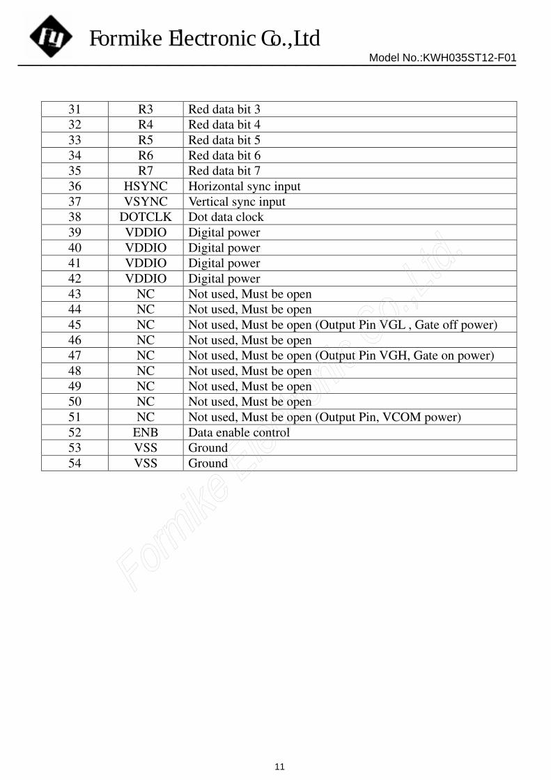
2.3 Timing Characteristics
Note : The interface of this module can drive by digital 24-bit data.
Formike Electronic Co.,LtdModel No.:KWH035ST12-F01 ___________________________________________
12

Note: The example transmit “0x1264h” to register R28h.
SPID connected to VSS.
SPI interface timing diagram & transaction example
Formike Electronic Co.,LtdModel No.:KWH035ST12-F01 ___________________________________________
13

2.4 Power Sequence
2.4.1 Power up sequence
Note: 1 The pin, SHUT be fixed to VSS. 2 The voltage of VDD be boost from VDDIO
Formike Electronic Co.,LtdModel No.:KWH035ST12-F01 ___________________________________________
14
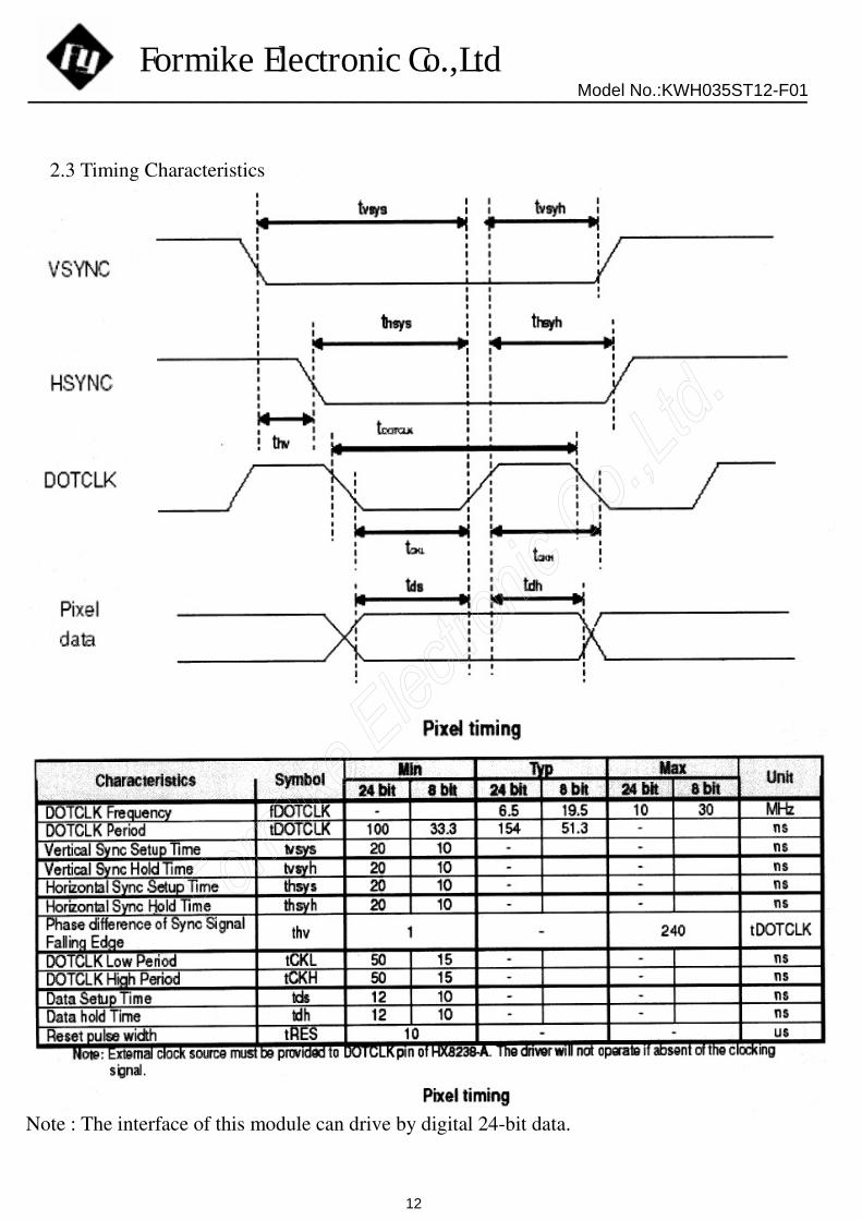
2.4.2 Power down sequence
Characteristics Symbol Min. Typ Max Unit
2 - - Frame Rising edge of SHUT to
display off
-1 line:408clk
-1 frame: 262line
-DOTCLK-6.5MHz
Tshul-off
33.4 - - ms
Input-signal-off to VDDD /
VDDIO off Toff-vdd 1 - - us
Note: DOTCLK must be maintained at lease 2 frames after the rising edge of SHUT
Display become off at the 2nd
falling edge of VSTNC after the falling edge of SHUT
If RESET signal is necessary for power down, provide it after the 2-frames-cycle of the SHUT peried.
Note 1: The pin, SHUT be fixed to VSS. 2: The voltage of VDD be boost from VDDIO.
Formike Electronic Co.,LtdModel No.:KWH035ST12-F01 ___________________________________________
15

3. QUALITY ASSURANCE SYSTEM 3.1 Quality Assurance Flow Chart
Formike Electronic Co.,LtdModel No.:KWH035ST12-F01 ___________________________________________
16

Formike Electronic Co.,LtdModel No.:KWH035ST12-F01 ___________________________________________
17

3.2 Inspection Specification
1. Inspection Specification
� Scope: The document shall be applied to TFT-LCD Module for 3.5”~10” (Ver.02)
� Inspection Standard: MIL-STD-105E Table Normal Inspection Single Sampling Level
II.
� Equipment: Gauge, MIL-STD Powertip Tester, Sample
� Defect Level: Major Defect AQL: 0.4 Minor Defect AQL:1.5
� OUT Going Defect Level: Sampling
� Standard of the product appearance test:
a: Manner of appearance test:
(1) The test best be under 20W*2 fluorescent light, and distance of view must be at
30cm.
(2) The test direction is base on about around 45∘of vertical line.
(3) Definition of area.
(4) Standard of inspection: (Unit: mm)
A area: viewing area
B area: Outside of viewing area
Formike Electronic Co.,LtdModel No.:KWH035ST12-F01 ___________________________________________
18

Specification For TFT-LCD Module 3.5”~10” (Ver.02)
Specification For TFT-LCD Module 3.5”~10” (Ver.02)
NO Item Criterion Level
1.1 The part number is inconsistent with work order of
production. Major
1.2 Mixed product types. Major 01
Product
condition
1.3 Assembled in inverse direction. Major
02 Quantity 2.1 The quantity is inconsistent with work order of production.
Major
03 Outling
dimension
3.1 Product dimension and structure must conform to structure
diagram. Major
4.1 Missing line character and icon. Major
4.2 No function or no display. Major
4.3 Display malfunction. Major
4.4 LCD viewing angle defect. Major 04
Electrical
Testing
4.5 Current consumption exceeds product specifications. Major
05
Dot defect
(Bright dot,
Dark dot)
On-display
Item Acceptance(Q’ty)
Bright Dot ≦4
Dark Dot ≦5
Joint Dot ≦3
Dot
Defect
Total ≦7
5.1 Inspection pattern: full white, full black, Red, Green and
blue screens.
5.2 It is defined as dot defect if defect area > 1/2 dot.
5.3 The distance between two dot defect ≧5mm.
Minor
Formike Electronic Co.,LtdModel No.:KWH035ST12-F01 ___________________________________________
19

Specification For TFT-LCD Module 3.5”~10” (Ver.02)
NO Item Criterion Level
06
Black or white
dot, scratch,
contamination
Round type
Ø=(x+y)/2
Line type
6.1 Round type (Non-display or display)
Dimension(diameter:Φ) Acceptance(Q’ty)
Φ≦0.25 Ignore
0.25<Φ≦0.50 5
Φ>0.50 0
Total 5
6.2 Line type(Non-display or display)
Length(L) Width(W) Acceptance(Q’ty)
--- W≦0.03 Ignore
L ≦10.0 0.03<W ≦0.05 4
L≦ 5.0 0.05< W ≦0.10 2
--- W> 0.10 As round type
Total 5
Minor
07 Polarizer
Bubble
Dimension(diameter:Φ) Acceptance (Q’ty)
Φ≦0.25 Ignore
0.25<Φ≦ 0.50 4
0.50< Φ≦0.80 1
Φ> 0.80 0
Total 5
Minor
Formike Electronic Co.,LtdModel No.:KWH035ST12-F01 ___________________________________________
20

Specification For TFT-LCD Module 3.5”~10” (Ver.02)
NO Item Criterion Level
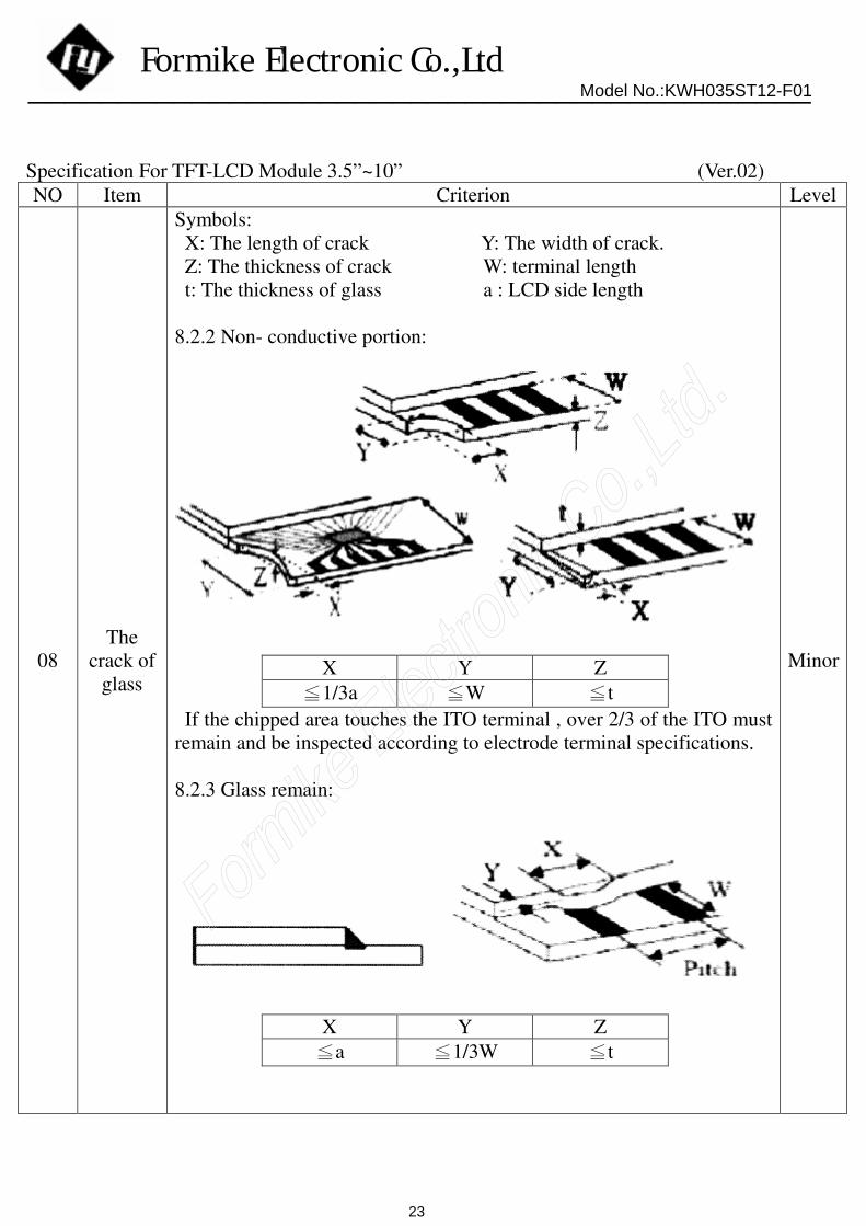
08 The crack of
glass
Symbols:
X: The length of crack Y: The width of crack.
Z: The thickness of crack W: terminal length
t : The thickness of glass a : LCD side length
8.1 General glass chip:
8.1.1 Chip on panel surface and crack between panels:
X Y Z
≦a Crack can’t enter
viewing area ≦1/2t
≦ Crack can’t exceed
the half of SP width 1/2t < Z≦2t
Minor
Formike Electronic Co.,LtdModel No.:KWH035ST12-F01 ___________________________________________
21

Specification For TFT-LCD Module 3.5”~10” (Ver.02)
NO Item Criterion Level
08 The crack
of glass
Symbols:
X: The length of crack Y: The width of crack.
Z: The thickness of crack W: terminal length
t : The thickness of glass a : LCD side length
8.1.2 Corner crack:
X Y Z
≦1/5a Crack can’t enter
viewing area Z ≦1/2t
≦1/5a Crack can’t exceed
the half of SP
width
1/2t < Z ≦2t
8.2 Protrusion over terminal:
8.2.1 Chip on electrode pad:
X Y Z
Front ≦a ≦1/2W ≦t
Back ≦a ≦W ≦1/2t
Minor
Formike Electronic Co.,LtdModel No.:KWH035ST12-F01 ___________________________________________
22
Specification For TFT-LCD Module 3.5”~10” (Ver.02)
NO Item Criterion Level
08
The
crack of
glass
Symbols:
X: The length of crack Y: The width of crack.
Z: The thickness of crack W: terminal length
t: The thickness of glass a : LCD side length
8.2.2 Non- conductive portion:
X Y Z
≦1/3a ≦W ≦t
If the chipped area touches the ITO terminal , over 2/3 of the ITO must
remain and be inspected according to electrode terminal specifications.
8.2.3 Glass remain:
X Y Z
≦a ≦1/3W ≦t
Minor
Formike Electronic Co.,LtdModel No.:KWH035ST12-F01 ___________________________________________
23

Specification For TFT-LCD Module 3.5”~10” (Ver.02)
NO Item Criterion Level
9.1 Backlight can’t work normally. Major
9.2 Backlight doesn’t light or color is wrong. Major 09 Backlight
Elements
9.3 Illumination source flickers when lit. Major
10.1 Pin type, quantity, dimension must match type in
structure diagram. Major
10.2 No short circuits in components on PCB or FPC. Major
10.3 Parts on PCB or FPC must be the same as on the
production characteristic chart. There should be no
wrong parts, missing parts or excess parts.
Major
10.4 Product packaging must the same as specified on
packaging specification sheet. Minor
10.5 The folding and peeled off in polarizer are not
acceptable. Minor
10 General
appearance
10.6 The PCB or FPC between B/L assembled distance
(PCB or FPC) is ≦1.5mm. Minor
Formike Electronic Co.,LtdModel No.:KWH035ST12-F01 ___________________________________________
24

4. RELIABILITY TEST 4.1 Reliability Test Condition Ver.02
Formike Electronic Co.,LtdModel No.:KWH035ST12-F01 ___________________________________________
25

5. PRECAUTION RELATING PRODUCT HANDLING 5.1 SAFETY
5.1.1 If the LCD panel breaks, be careful not to get the liquid crystal to touch your skin.
5.1.2 If the liquid crystal touches your skin or clothes, please wash it off immediately by using
soap and water.
5.2 HANDLING
5.2.1 Avoid any strong mechanical shock which can break the glass.
5.2.2 Avoid static electricity which can damage the CMOS LSI-When working with the module,
be sure to ground your body and any electrical equipment you may be using.
5.2.3 Do not remove the panel or frame from the module.
5.2.4 The polarizing plate of the display is very fragile. So, please handle it very carefully, do not
touch, push or rub the exposed polarizing with anything harder than an HB pencil lead
(glass, tweezers, etc.)
5.2.5 Do not wipe the polarizing plate with a dry cloth, as it may easily scratch the surface of
plate.
5.2.6 Do not touch the display area with bare hands, this will stain the display area.
5.2.7 Do not use ketonics solvent & aromatic solvent. Use with a soft cloth soaked with a
cleaning naphtha solvent.
5.2.8 To control temperature and time of soldering is 320±10℃ and 3-5 sec.
5.2.9 To avoid liquid (include organic solvent) stained on LCM.
5.3 STORAGE
5.3.1 Store the panel or module in a dark place where the temperature is 25℃±5℃ and the
humidity is below 65% RH.
5.3.2 Do not place the module near organics solvents or corrosive gases.
5.3.3 Do not crush, shake, or jolt the module.
5.4 TERMS OF WARRANTY
5.4.1 Applicable warrant period
The period is within thirteen months since the date of shipping out under normal using and
storage conditions.
5.4.2 Unaccepted responsibility
This product has been manufactured to your company’s specification as a part for use in your
company’s general electronic products. It is guaranteed to perform according to delivery
specifications. For any other use apart from general electronic equipment, we cannot take
responsibility if the product is used in nuclear power control equipment, aerospace equipment,
fire and security systems or any other applications in which there is a direct risk to human life
and where extremely high levels of reliability are required.
Formike Electronic Co.,LtdModel No.:KWH035ST12-F01 ___________________________________________
26

Formike Electronic Co.,LtdModel No.:KWH035ST12-F01 ___________________________________________
27