Embed Size (px)
Citation preview
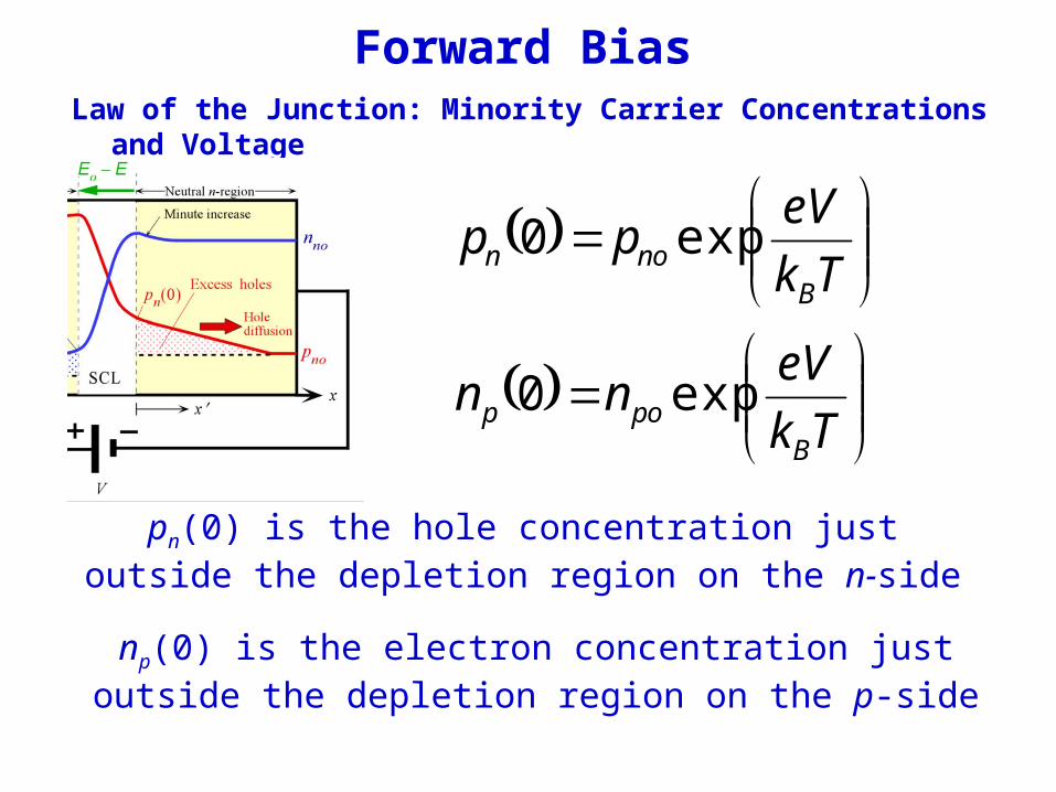
Forward BiasLaw of the Junction: Minority Carrier Concentrations and Voltage
Tk
eVnn
Tk
eVpp
Bpop
Bnon
exp0
exp0
np(0) is the electron concentration just outside the depletion region on the p-side
pn(0) is the hole concentration just outside the depletion region on the n-side
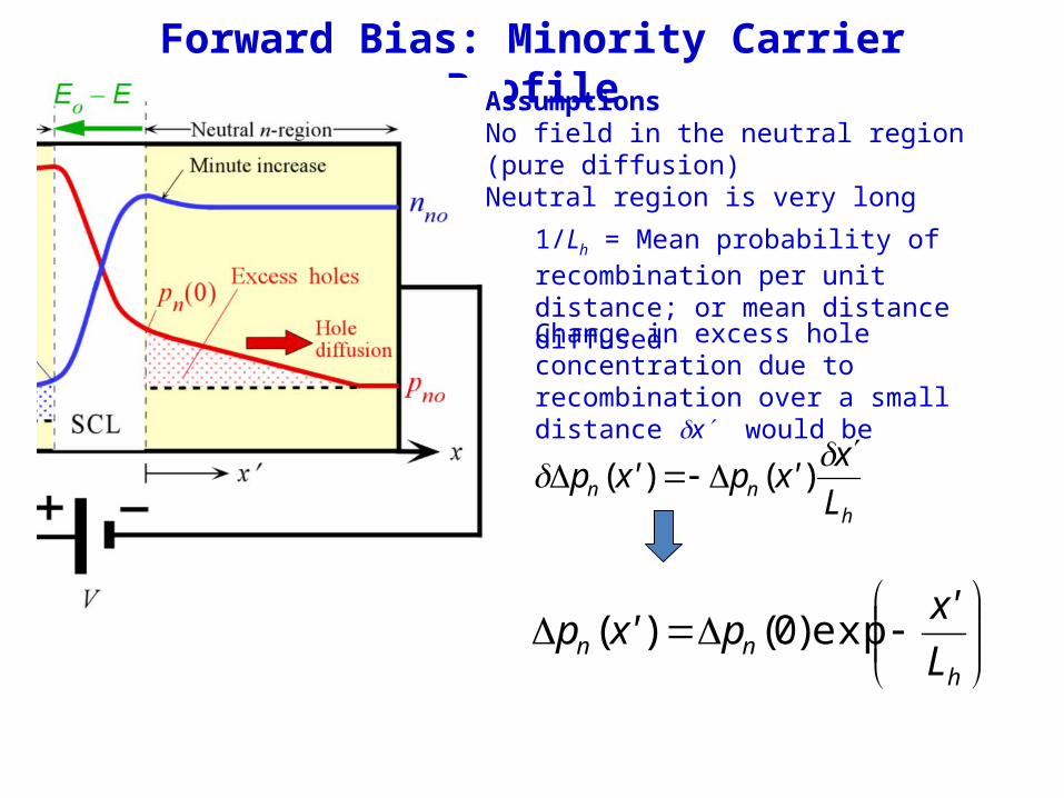
Forward Bias: Minority Carrier Profile
hnn L
xx'px'p
)()(
AssumptionsNo field in the neutral region (pure diffusion)Neutral region is very long
1/Lh = Mean probability of recombination per unit distance; or mean distance diffused
Change in excess hole concentration due to recombination over a small distance dx would be
hnn L
x'px'p exp)0()(
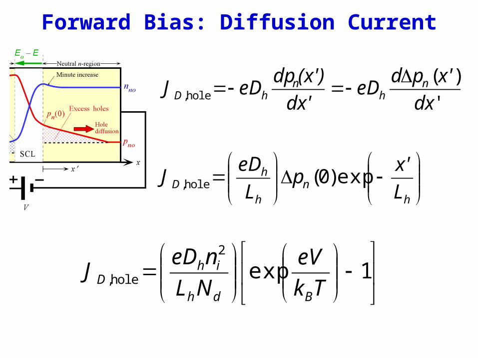
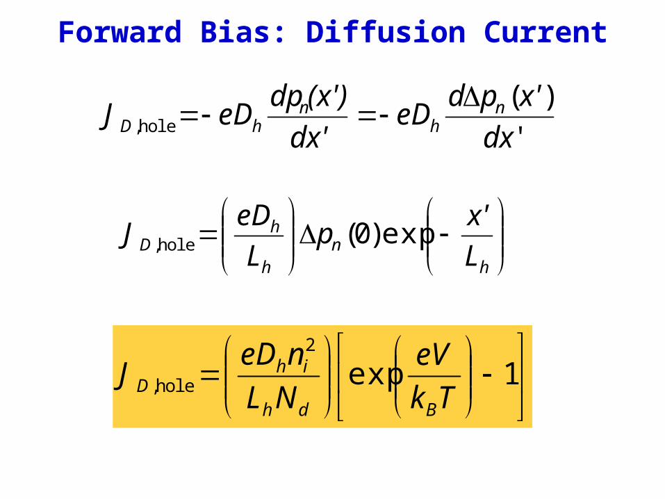
Forward Bias: Diffusion Current
'
)(hole, dx
x'pdeD
dx'
(x')dpeDJ n
hn
hD
hn
h
hD L
x'p
L
eDJ exp)0(hole,
1exp
2
hole, Tk
eV
NL
neDJ
Bdh
ihD
Forward Bias: Diffusion Current
'
)(hole, dx
x'pdeD
dx'
(x')dpeDJ n
hn
hD
hn
h
hD L
x'p
L
eDJ exp)0(hole,
1exp
2
hole, Tk
eV
NL
neDJ
Bdh
ihD
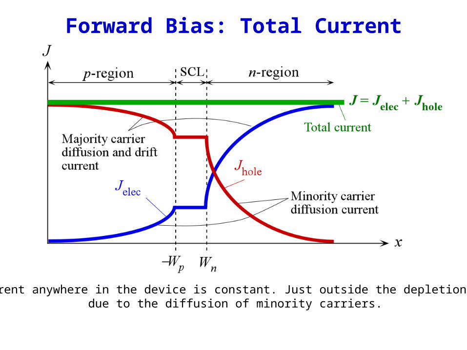
The total current anywhere in the device is constant. Just outside the depletion region it is due to the diffusion of minority carriers.
Forward Bias: Total Current
Forward Bias: Diffusion Current
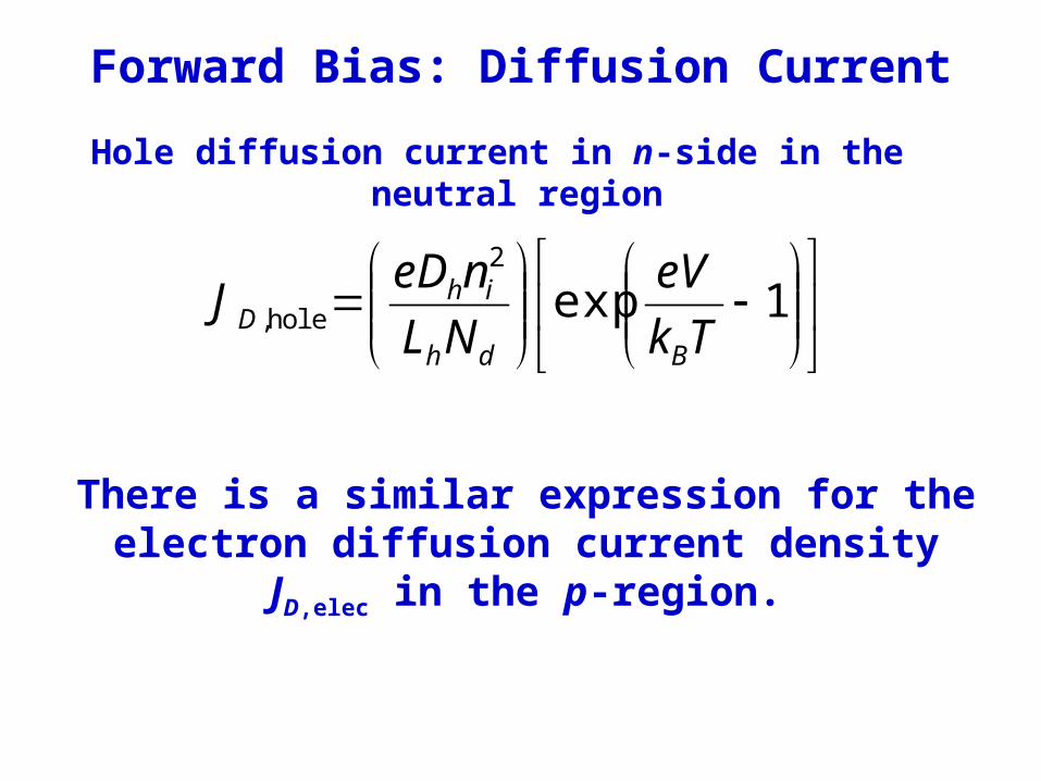
Hole diffusion current in n-side in the neutral region
1exp
2
hole, Tk
eV
NL
neDJ
Bdh
ihD
There is a similar expression for the electron diffusion current density JD,elec in the p-region.
Forward Bias: Diffusion Current
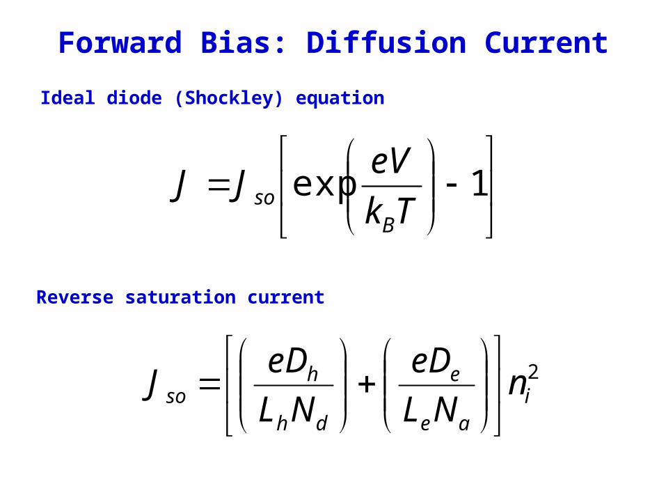
Ideal diode (Shockley) equation
1exp
Tk
eVJJ
Bso
2i
ae
e
dh
hso n
NL
eD
NL
eDJ
Reverse saturation current
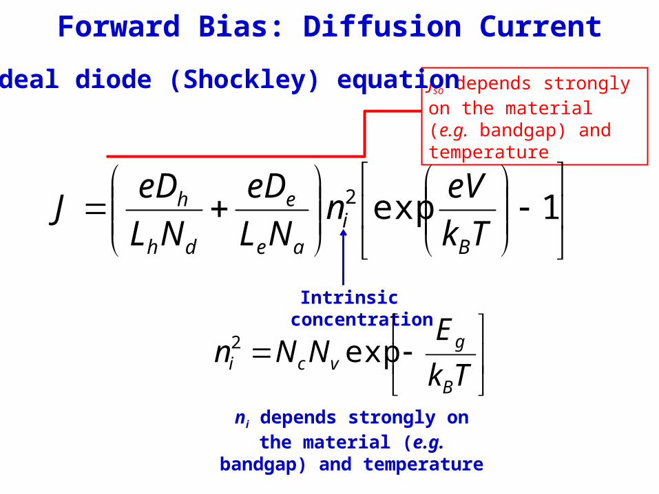
Forward Bias: Diffusion Current
1exp2
Tk
eVn
NL
eD
NL
eDJ
Bi
ae
e
dh
h
Intrinsic concentration
Tk
ENNn
B
gvci exp2
Jso depends strongly on the material (e.g. bandgap) and temperature
ni depends strongly on the material (e.g. bandgap) and temperature
Ideal diode (Shockley) equation
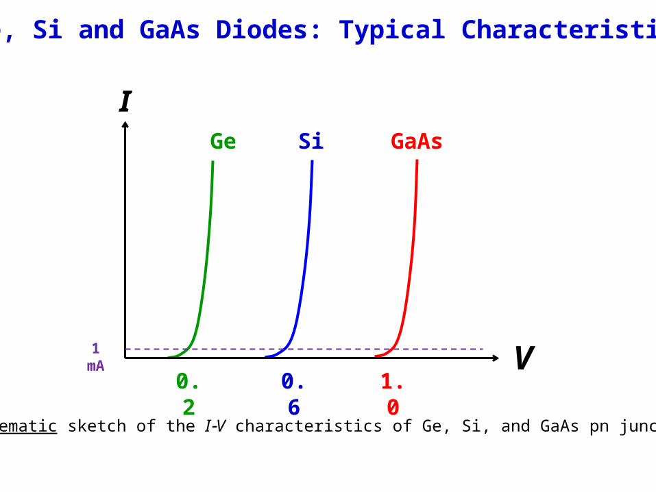
Schematic sketch of the I-V characteristics of Ge, Si, and GaAs pn junctions.
V
I
0.2 0.6 1.0
Ge Si GaAs
Ge, Si and GaAs Diodes: Typical Characteristics
1 mA
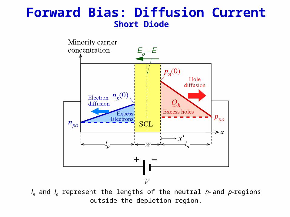
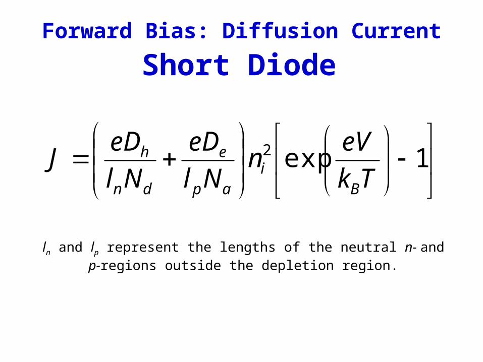
Forward Bias: Diffusion CurrentShort Diode
ln and lp represent the lengths of the neutral n- and p-regions outside the depletion region.
Forward Bias: Diffusion Current
Short Diode
1exp2
Tk
eVn
Nl
eD
Nl
eDJ
Bi
ap
e
dn
h
ln and lp represent the lengths of the neutral n- and p-regions outside the depletion region.
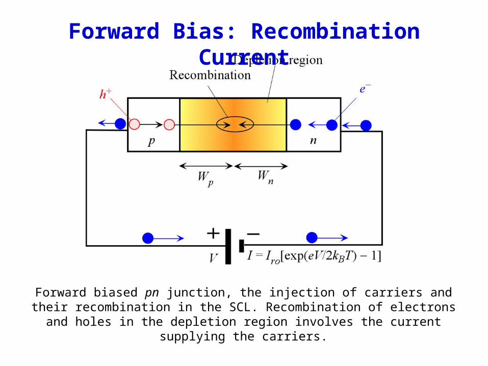
Forward Bias: Recombination Current
Forward biased pn junction, the injection of carriers and their recombination in the SCL. Recombination of electrons and holes in the depletion region involves the current
supplying the carriers.
Forward Bias: Recombination Current
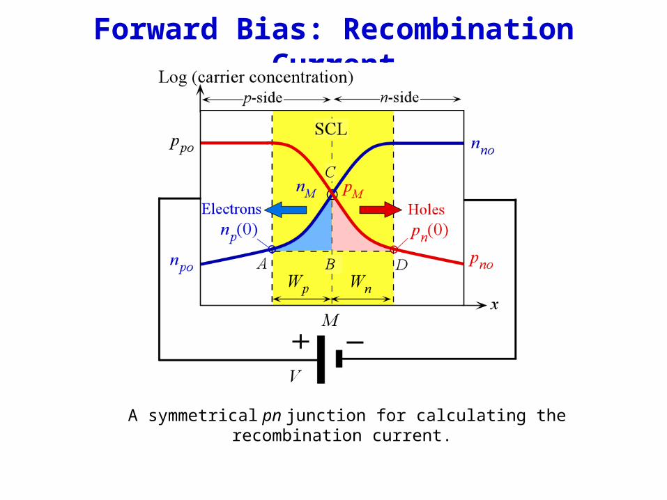
A symmetrical pn junction for calculating the recombination current.
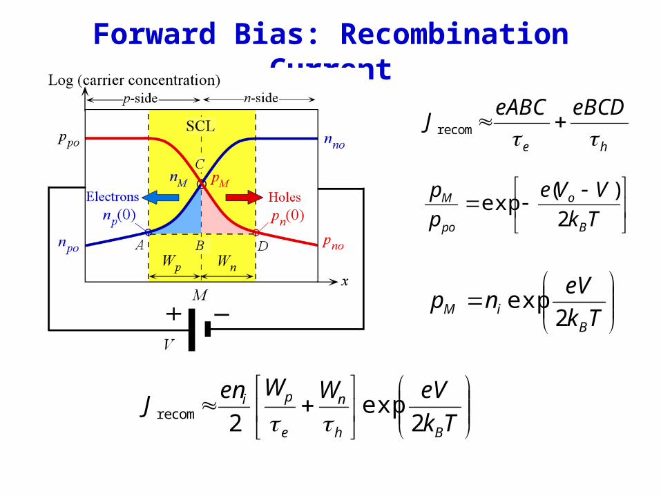
Forward Bias: Recombination Current
he
eBCDeABCJ
recom
Tk
VVe
p
p
B
o
po
M
2
)(exp
Tk
eVnp
BiM 2exp
Tk
eVWWenJ
Bh
n
e
pi
2exp
2recom
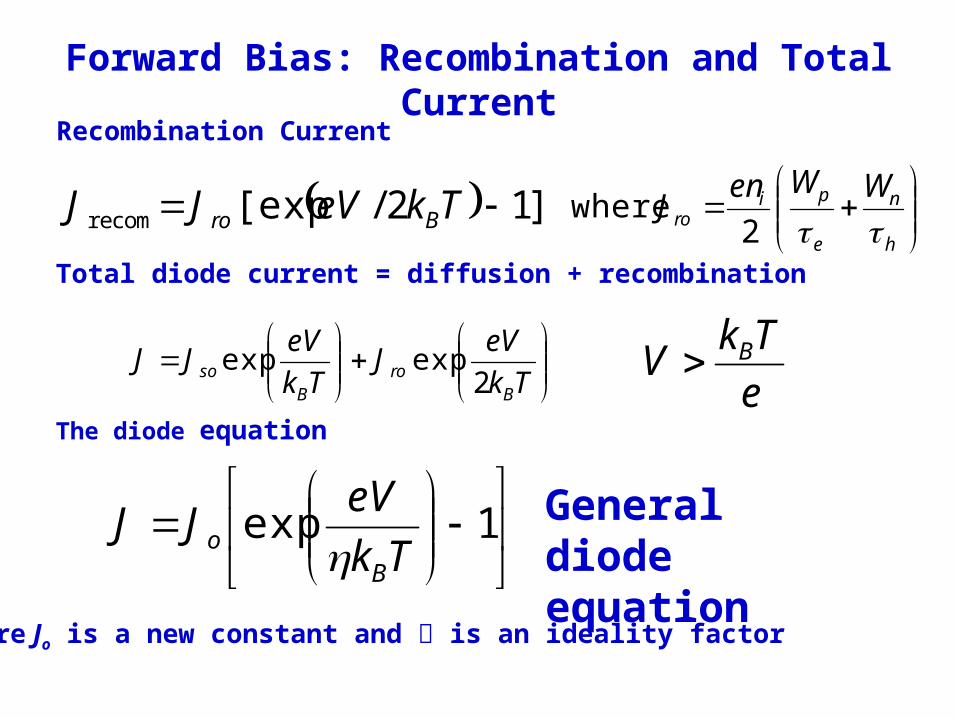
Forward Bias: Recombination and Total Current
Recombination Current
]12/[exprecom TkeVJJ Bro
Tk
eVJ
Tk
eVJJ
Bro
Bso 2
expexp
Total diode current = diffusion + recombination
e
TkV B
The diode equation
h
n
e
piro
WWenJ
2 where
1exp
Tk
eVJJ
Bo
where Jo is a new constant and is an ideality factor
General diode equation
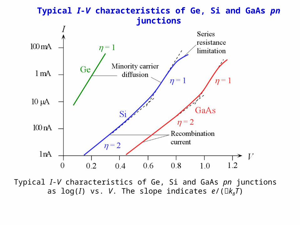
Typical I-V characteristics of Ge, Si and GaAs pn junctions as log(I) vs. V. The slope indicates e/(kBT)
Typical I-V characteristics of Ge, Si and GaAs pn junctions
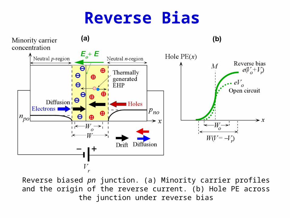
Reverse biased pn junction. (a) Minority carrier profiles and the origin of the reverse current. (b) Hole PE across the junction under reverse bias
Reverse Bias
Reverse Bias
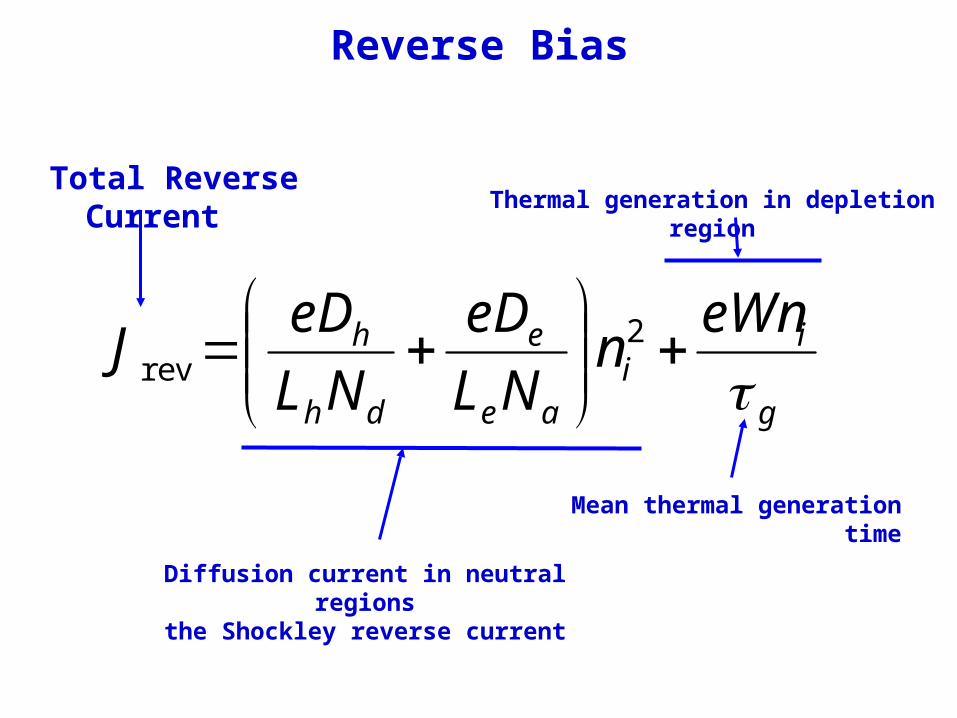
Total Reverse Current
g
ii
ae
e
dh
h eWnn
NL
eD
NL
eDJ
2
rev
Mean thermal generation time
Diffusion current in neutral regionsthe Shockley reverse current
Thermal generation in depletion region
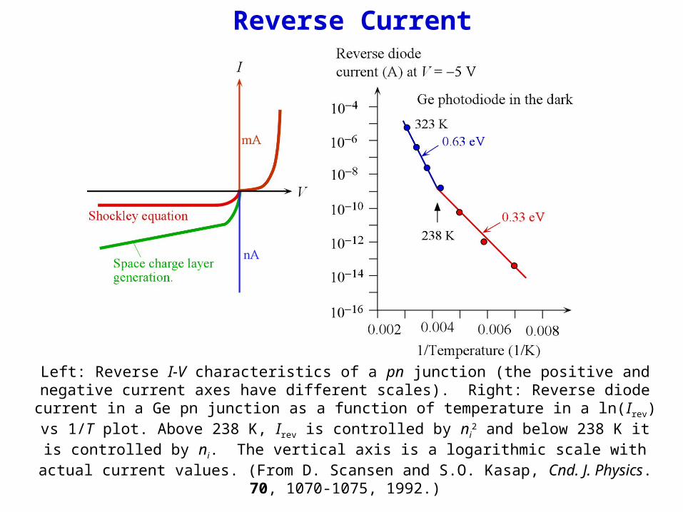
Left: Reverse I-V characteristics of a pn junction (the positive and negative current axes have different scales). Right: Reverse diode current in a Ge pn junction as a function of temperature in a ln(Irev) vs 1/T plot. Above 238 K, Irev is controlled by ni
2 and below 238 K it is controlled by ni. The vertical axis is a logarithmic scale with actual current values. (From D. Scansen and S.O. Kasap, Cnd. J. Physics. 70,
1070-1075, 1992.)
Reverse Current
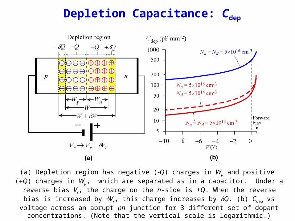
(a) Depletion region has negative (-Q) charges in Wp and positive (+Q) charges in Wp, which are separated as in a capacitor. Under a reverse bias Vr, the charge on the n-side is +Q. When the reverse bias is increased by dVr, this charge increases by dQ. (b) Cdep vs voltage across an abrupt pn junction
for 3 different set of dopant concentrations. (Note that the vertical scale is logarithmic.)
Depletion Capacitance: Cdep
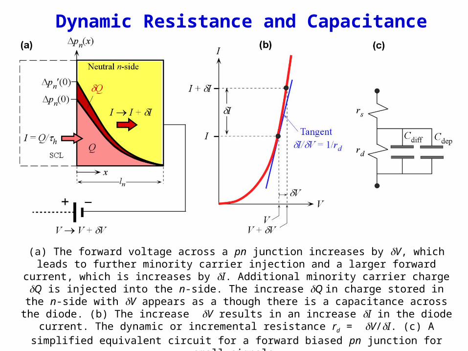
(a) The forward voltage across a pn junction increases by dV, which leads to further minority carrier injection and a larger forward current, which is increases by dI. Additional minority carrier charge dQ is injected into the n-side. The increase dQ in charge stored in the n-side with dV appears as a though
there is a capacitance across the diode. (b) The increase dV results in an increase dI in the diode current. The dynamic or incremental resistance rd = dV/dI. (c) A simplified equivalent circuit for a
forward biased pn junction for small signals.
Dynamic Resistance and Capacitance
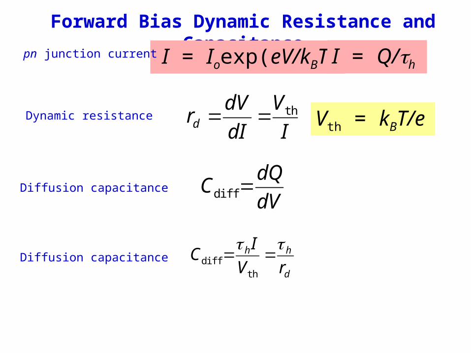
Forward Bias Dynamic Resistance and Capacitance
I = Ioexp(eV/kBT)
I
V
dI
dVrd
th Vth = kBT/e Dynamic resistance
dV
dQC diffDiffusion capacitance
I = Q/th
d
hh
rV
IC
thdiff
pn junction current
Diffusion capacitance
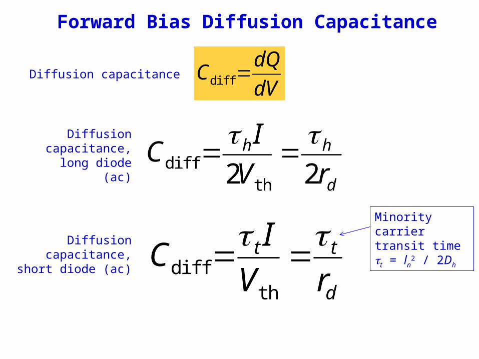
Forward Bias Diffusion Capacitance
dV
dQC diffDiffusion capacitance
d
hh
rV
IC
22 thdiff
d
tt
rV
IC
thdiff
Diffusion capacitance, long
diode (ac)
Diffusion capacitance, short diode (ac)
Minority carrier transit timett = ln
2 / 2Dh
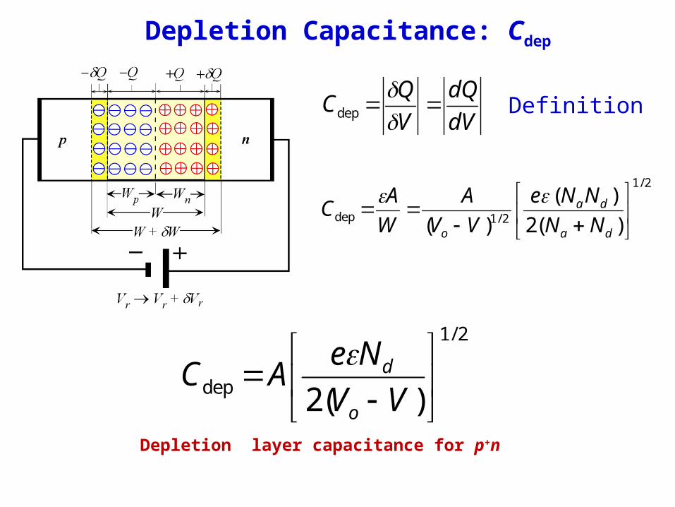
Depletion Capacitance: Cdep
dV
dQ
V
QC
dep
2/1
2/1dep )(2
)(
)(
da
da
o NN
NNe
VV
A
W
AC
Definition
2/1
dep )(2
VV
NeAC
o
d
Depletion layer capacitance for p+n
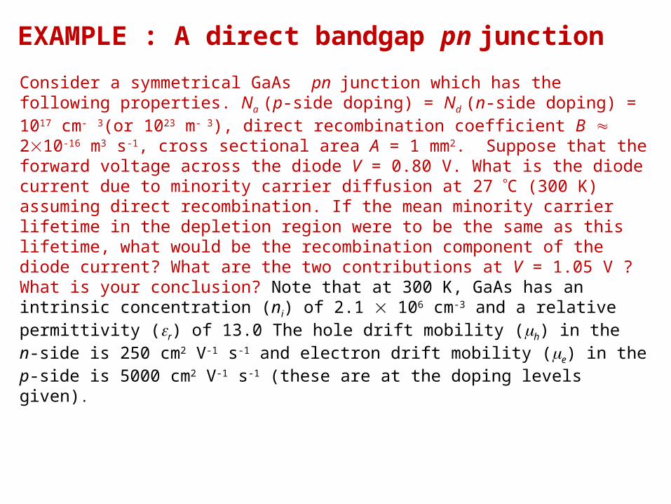
EXAMPLE : A direct bandgap pn junction
Consider a symmetrical GaAs pn junction which has the following properties. Na (p-side doping) = Nd (n-side doping) = 1017 cm- 3(or 1023 m- 3), direct recombination coefficient B 210-16 m3 s-1, cross sectional area A = 1 mm2. Suppose that the forward voltage across the diode V = 0.80 V. What is the diode current due to minority carrier diffusion at 27 C (300 K) assuming direct recombination. If the mean minority carrier lifetime in the depletion region were to be the same as this lifetime, what would be the recombination component of the diode current? What are the two contributions at V = 1.05 V ? What is your conclusion? Note that at 300 K, GaAs has an intrinsic concentration (ni) of 2.1 106 cm-3 and a relative permittivity (er) of 13.0 The hole drift mobility (mh) in the n-side is 250 cm2 V-1 s-1 and electron drift mobility (me) in the p-side is 5000 cm2 V-1 s-1 (these are at the doping levels given).
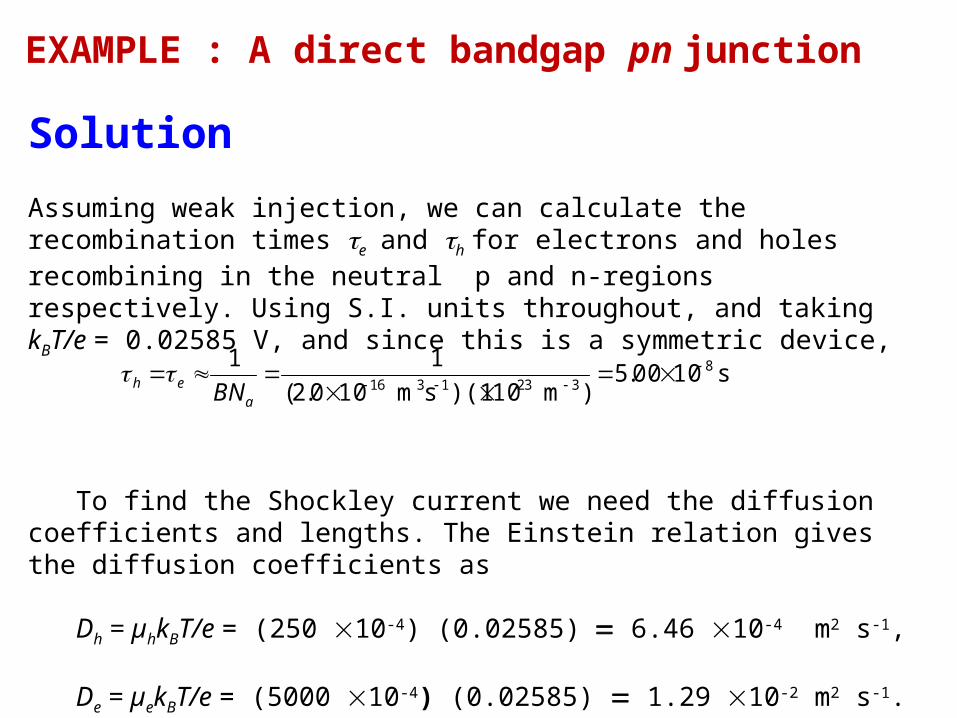
EXAMPLE : A direct bandgap pn junction
Solution
Assuming weak injection, we can calculate the recombination times te and th for electrons and holes recombining in the neutral p and n-regions respectively. Using S.I. units throughout, and taking kBT/e = 0.02585 V, and since this is a symmetric device,
To find the Shockley current we need the diffusion coefficients and lengths. The Einstein relation gives the diffusion coefficients as
Dh = µhkBT/e = (250 10-4) (0.02585) = 6.46 10-4 m2 s-1,
De = µekBT/e = (5000 10-4) (0.02585) = 1.29 10-2 m2 s-1.
s1000.5)m 10)(1sm 100.2(
11 83231316
aeh BN
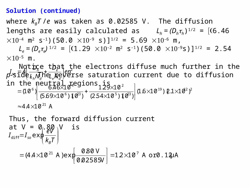
Solution (continued)
where kBT /e was taken as 0.02585 V. The diffusion lengths are easily calculated as Lh = (Dhth)1/2 = [(6.46 10-4 m2 s-1)(50.0 10-9 s)]1/2 = 5.69 10-6 m,Le = (Dete) 1/2 = [(1.29 10-2 m2 s-1)(50.0 10-9s)]1/2 = 2.54 10-5 m.Notice that the electrons diffuse much further in the p-side. The reverse
saturation current due to diffusion in the neutral regions is
A 104.4
)101.2)(106.1()10)(1054.2(
1029.1
)10)(1069.5(
1046.6)10(
21
21219235
2
236
46
2
i
ae
e
dh
hso en
NL
D
NL
DAI
μA 0.12orA 102.1V 02585.0
V 80.0exp)A 104.4(
exp
721
diff
Tk
eVII
Bso
Thus, the forward diffusion current at V = 0.80 V is
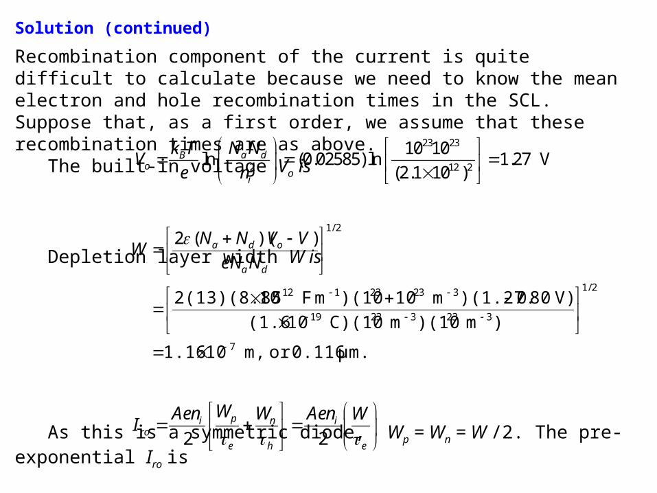
Solution (continued)
Recombination component of the current is quite difficult to calculate because we need to know the mean electron and hole recombination times in the SCL. Suppose that, as a first order, we assume that these recombination times are as above.
The built-in voltage Vo is
Depletion layer width W is
As this is a symmetric diode, Wp = Wn = W /2. The pre-exponential Iro is
23 23
2 12 2
10 10ln (0.02585) ln 1.27 V
(2.1 10 )a dB
oi
N Nk TV
e n
μm. 0.116or m, 101.16
)m )(10m C)(10 10(1.6
V) 80.0)(1.27m 10)(10m F 102(13)(8.85
))((2
7
2/1
32332319
32323112
2/1
da
oda
NeN
VVNNW
2 2pi n i
roe h e
WAen W Aen WI
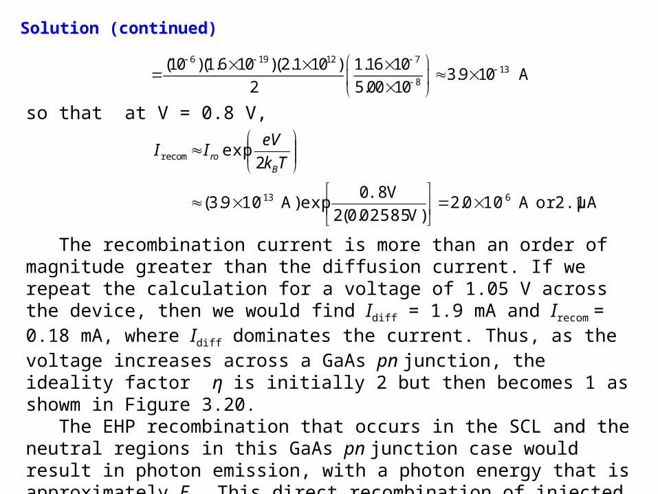
Solution (continued)
6 19 12 713
8
(10 )(1.6 10 )(2.1 10 ) 1.16 103.9 10 A
2 5.00 10
so that at V = 0.8 V,
The recombination current is more than an order of magnitude greater than the diffusion current. If we repeat the calculation for a voltage of 1.05 V across the device, then we would find Idiff = 1.9 mA and Irecom = 0.18 mA, where Idiff dominates the current. Thus, as the voltage increases across a GaAs pn junction, the ideality factor η is initially 2 but then becomes 1 as showm in Figure 3.20.
The EHP recombination that occurs in the SCL and the neutral regions in this GaAs pn junction case would result in photon emission, with a photon energy that is approximately Eg. This direct recombination of injected minority carriers and the resulting emission of photons represent the principle of operation of the Light Emitting Diode (LED).
μA 2.1orA 100.2)V 02585.0(2
V .80exp)A 109.3(
2exp
613
recom
Tk
eVII
Bro
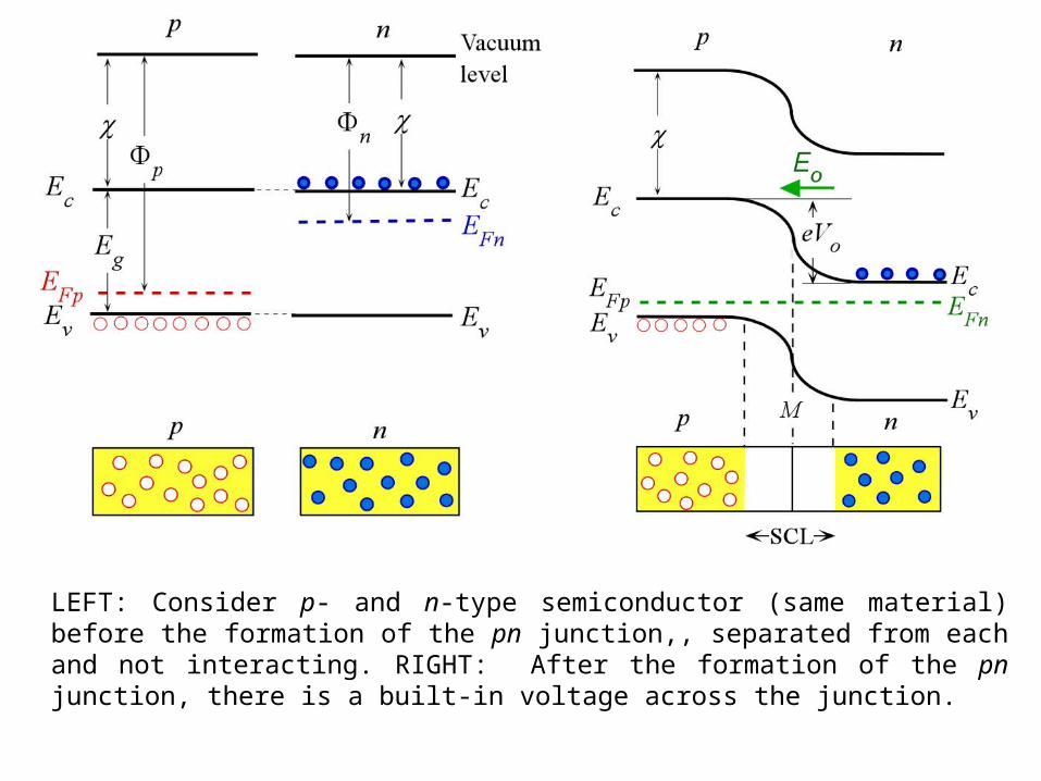
LEFT: Consider p- and n-type semiconductor (same material) before the formation of the pn junction,, separated from each and not interacting. RIGHT: After the formation of the pn junction, there is a built-in voltage across the junction.
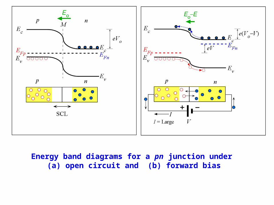
Energy band diagrams for a pn junction under (a) open circuit and (b) forward bias
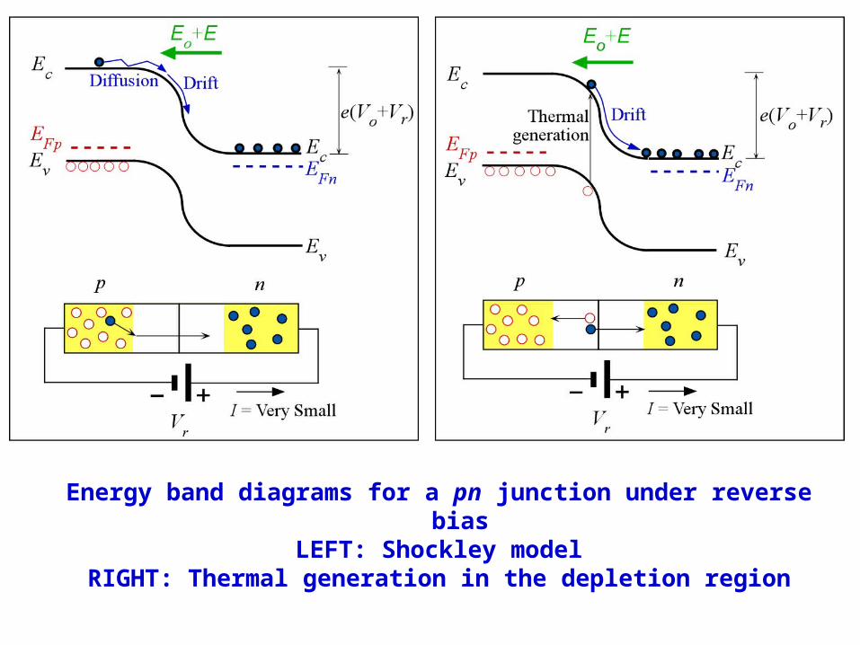
Energy band diagrams for a pn junction under reverse biasLEFT: Shockley model
RIGHT: Thermal generation in the depletion region
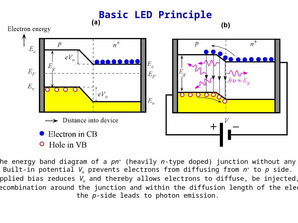
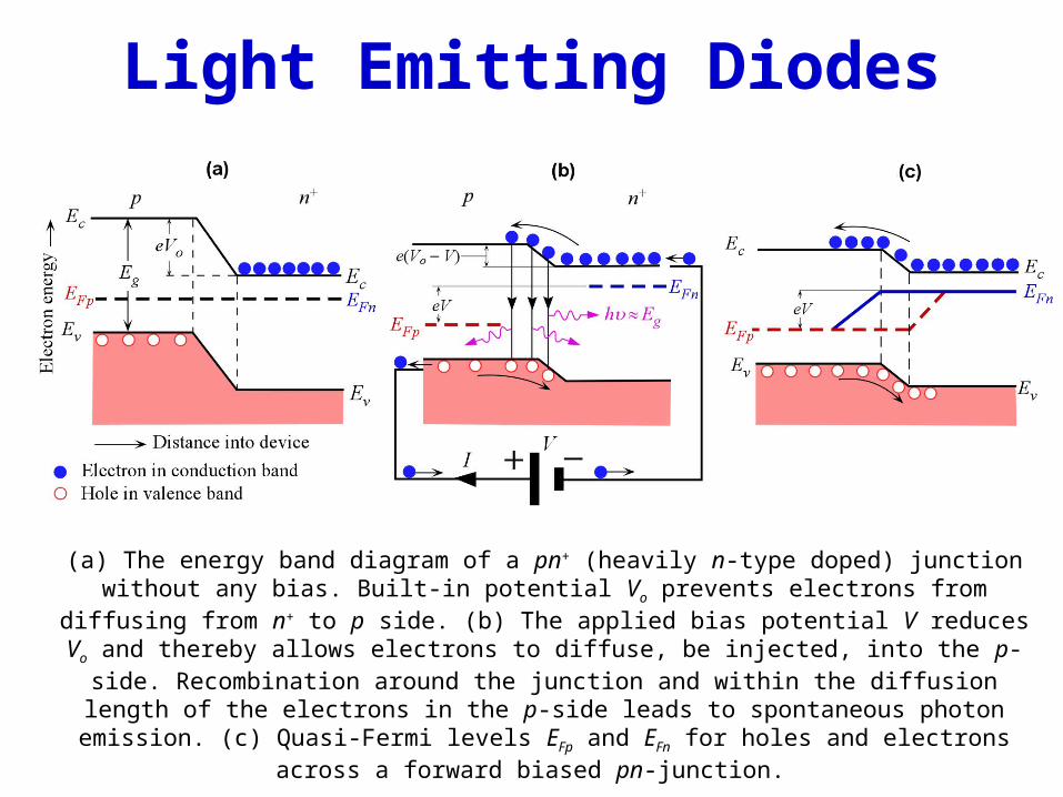
(a) The energy band diagram of a pn+ (heavily n-type doped) junction without any bias.Built-in potential Vo prevents electrons from diffusing from n+ to p side.
(b) The applied bias reduces Vo and thereby allows electrons to diffuse, be injected, into thep-side. Recombination around the junction and within the diffusion length of the electrons in
the p-side leads to photon emission.
Basic LED Principle

Light Emitting Diodes
(a) The energy band diagram of a pn+ (heavily n-type doped) junction without any bias. Built-in potential Vo prevents electrons from diffusing from n+ to p side. (b) The applied bias potential V reduces
Vo and thereby allows electrons to diffuse, be injected, into the p-side. Recombination around the junction and within the diffusion length of the electrons in the p-side leads to spontaneous photon emission. (c) Quasi-Fermi levels EFp and EFn for holes and electrons across a forward biased pn-
junction.
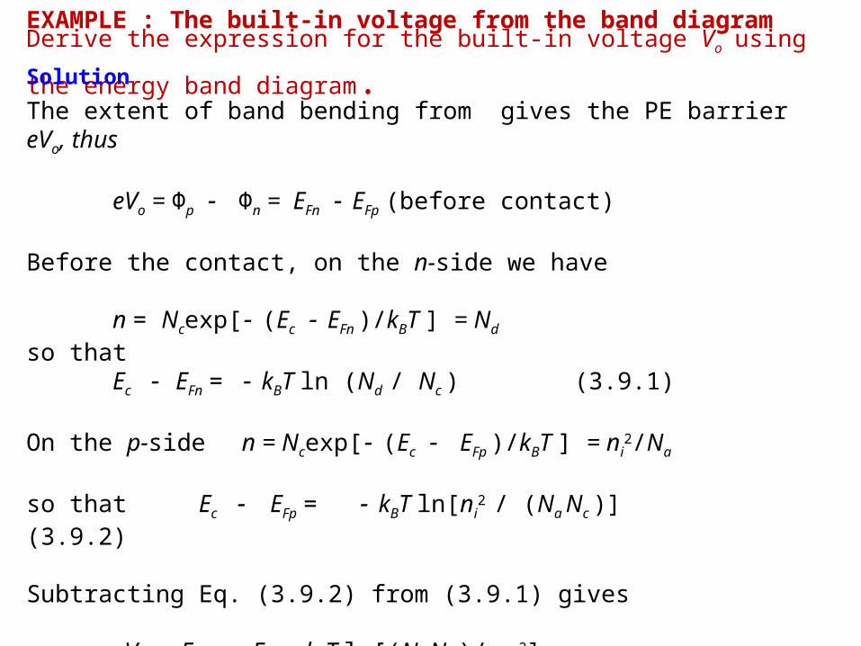
EXAMPLE : The built-in voltage from the band diagram
The extent of band bending from gives the PE barrier eVo, thus
eVo = Φp - Φn = EFn - EFp (before contact)
Before the contact, on the n-side we have
n = Ncexp[- (Ec - EFn )/kBT ] = Nd
so thatEc - EFn = - kBT ln (Nd / Nc ) (3.9.1)
On the p-side n = Ncexp[- (Ec - EFp )/kBT ] = ni2/Na
so that Ec - EFp = - kBT ln[ni2 / (Na Nc )] (3.9.2)
Subtracting Eq. (3.9.2) from (3.9.1) gives
eVo = EFn - EFp = kBT ln[(Na Nd )/ ni2]
Derive the expression for the built-in voltage Vo using the energy band diagram.Solution
Light Emitting Diodes
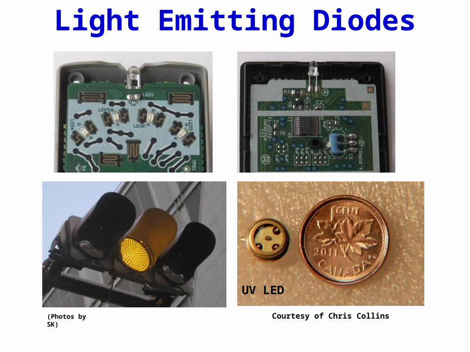
UV LED
Courtesy of Chris Collins(Photos by SK)
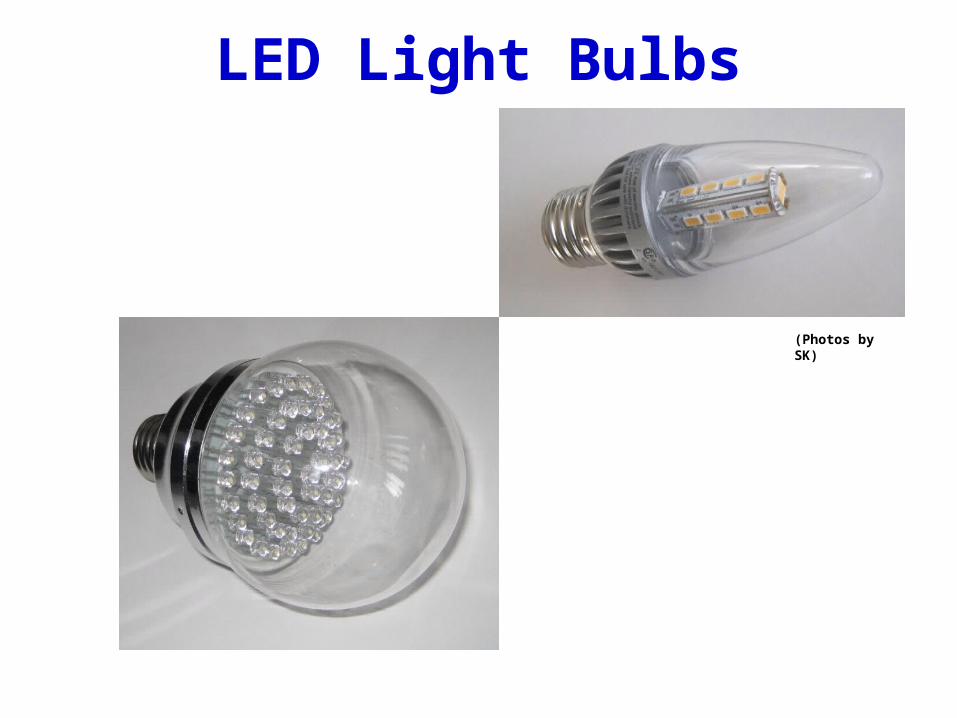
LED Light Bulbs
(Photos by SK)
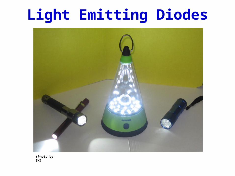
Light Emitting Diodes
(Photo by SK)
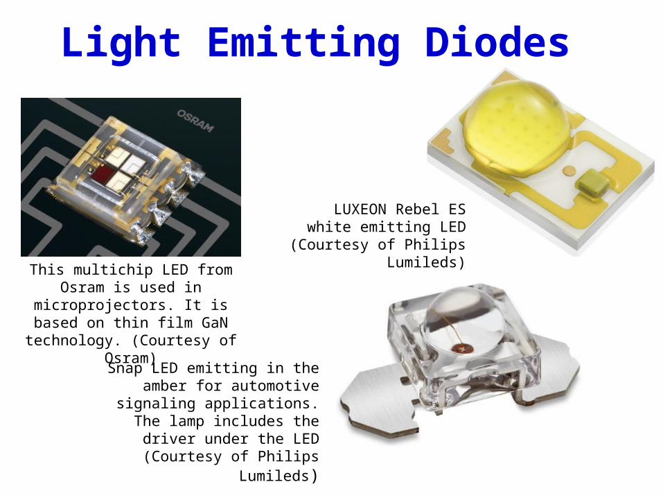
Light Emitting Diodes
This multichip LED from Osram is used in microprojectors. It is based on thin film GaN technology. (Courtesy of
Osram)
Snap LED emitting in the amber for automotive signaling applications. The
lamp includes the driver under the LED (Courtesy of Philips Lumileds)
LUXEON Rebel ES white emitting LED (Courtesy of
Philips Lumileds)

Microprojector using LEDs
A handheld microprojector MPro120 from 3M for projecting photos and videos on a wall uses LEDs for its projection light. (Courtesy fo 3M)
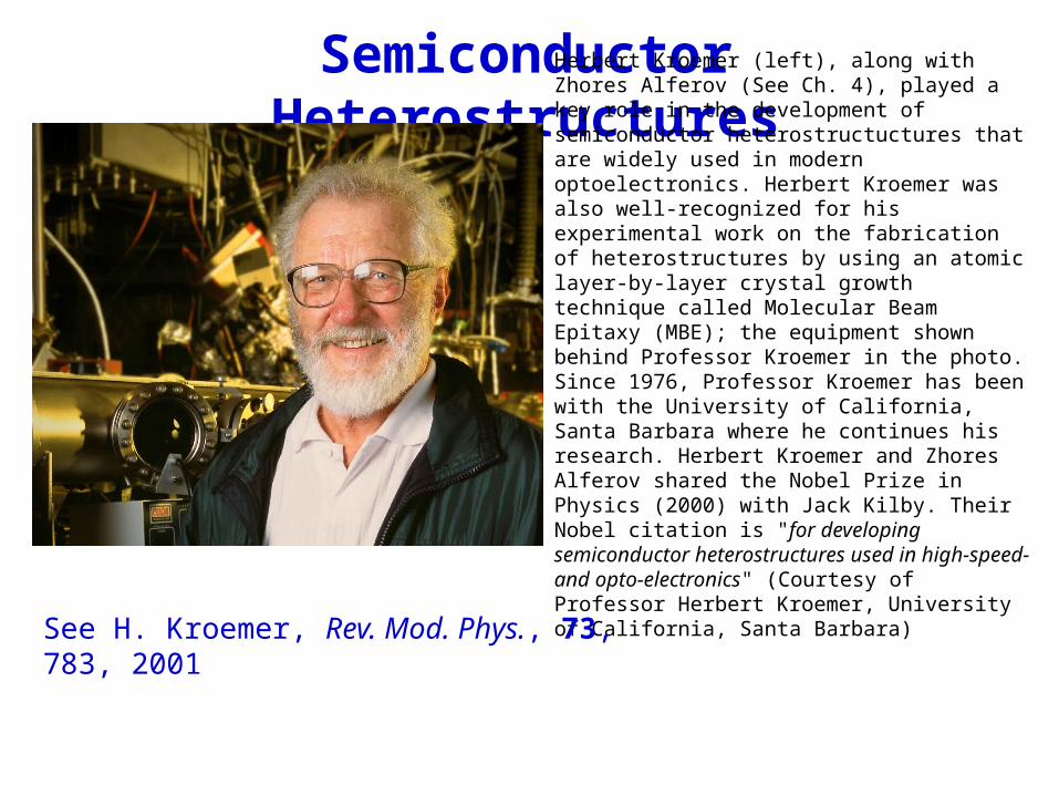
Semiconductor HeterostructuresHerbert Kroemer (left), along with Zhores Alferov (See Ch. 4), played a key role in the development of semiconductor heterostructuctures that are widely used in modern optoelectronics. Herbert Kroemer was also well-recognized for his experimental work on the fabrication of heterostructures by using an atomic layer-by-layer crystal growth technique called Molecular Beam Epitaxy (MBE); the equipment shown behind Professor Kroemer in the photo. Since 1976, Professor Kroemer has been with the University of California, Santa Barbara where he continues his research. Herbert Kroemer and Zhores Alferov shared the Nobel Prize in Physics (2000) with Jack Kilby. Their Nobel citation is "for developing semiconductor heterostructures used in high-speed- and opto-electronics" (Courtesy of Professor Herbert Kroemer, University of California, Santa Barbara)
See H. Kroemer, Rev. Mod. Phys., 73, 783, 2001
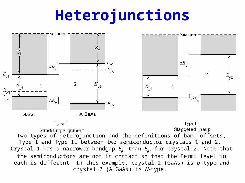
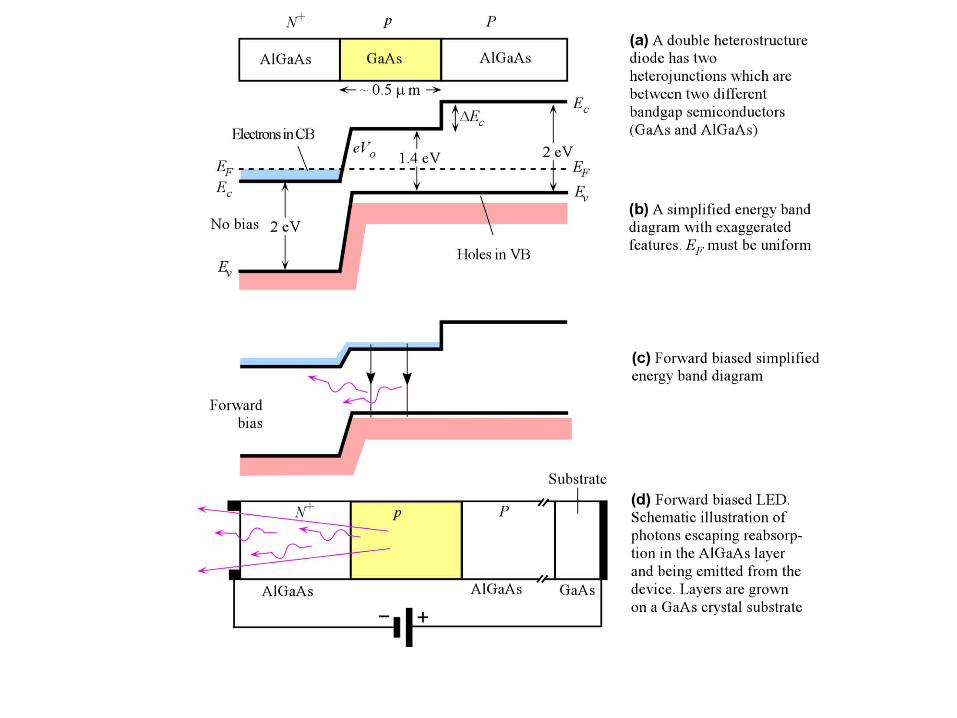
Heterojunctions
Two types of heterojunction and the definitions of band offsets, Type I and Type II between two semiconductor crystals 1 and 2. Crystal 1 has a narrower bandgap Eg1 than Eg2 for crystal 2. Note that
the semiconductors are not in contact so that the Fermi level in each is different. In this example, crystal 1 (GaAs) is p-type and crystal 2 (AlGaAs) is N-type.
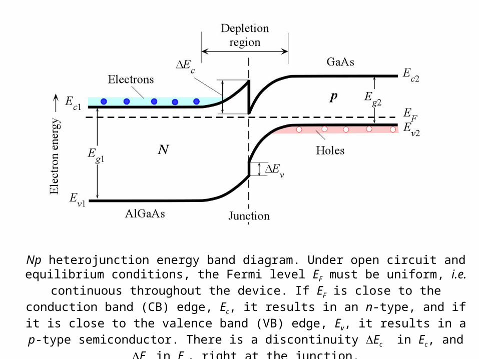
Np heterojunction energy band diagram. Under open circuit and equilibrium conditions, the Fermi level EF must be uniform, i.e. continuous throughout the device. If EF is close to the conduction band (CB) edge, Ec, it results in an n-type, and if it is close to the valence band (VB) edge, Ev, it results in a p-type semiconductor. There is a discontinuity DEc in Ec, and
DEv in Ev, right at the junction.
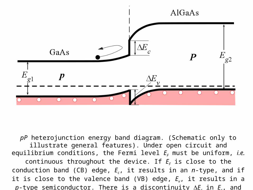
pP heterojunction energy band diagram. (Schematic only to illustrate general features). Under open circuit and equilibrium conditions, the Fermi level EF must be uniform, i.e. continuous throughout the device. If EF is close to the conduction band (CB) edge, Ec, it
results in an n-type, and if it is close to the valence band (VB) edge, Ev, it results in a p-type semiconductor. There is a discontinuity DEc in Ec, and DEv in Ev, right at the junction.
Light Emitting Diodes
(a) The energy band diagram of a pn+ (heavily n-type doped) junction without any bias. Built-in potential Vo prevents electrons from diffusing from n+ to p side. (b) The applied bias potential V reduces
Vo and thereby allows electrons to diffuse, be injected, into the p-side. Recombination around the junction and within the diffusion length of the electrons in the p-side leads to spontaneous photon emission. (c) Quasi-Fermi levels EFp and EFn for holes and electrons across a forward biased pn-
junction.
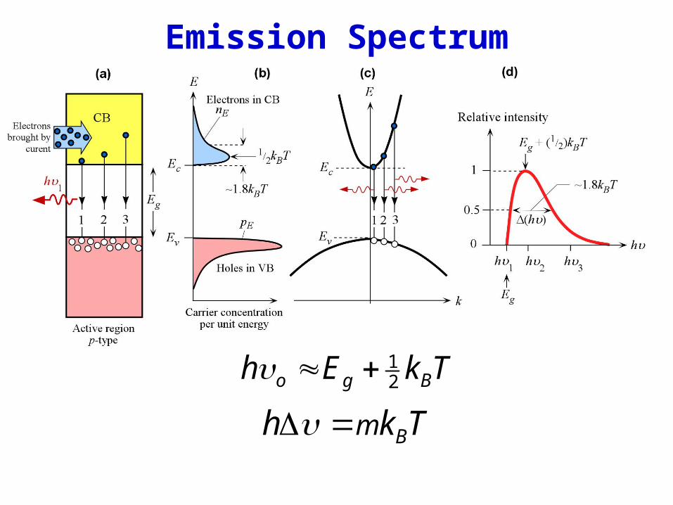
Emission Spectrum
TkEh Bgo 21
Tkh Bm
Emission Spectrum
TkEh Bgo 21
Tkh Bm
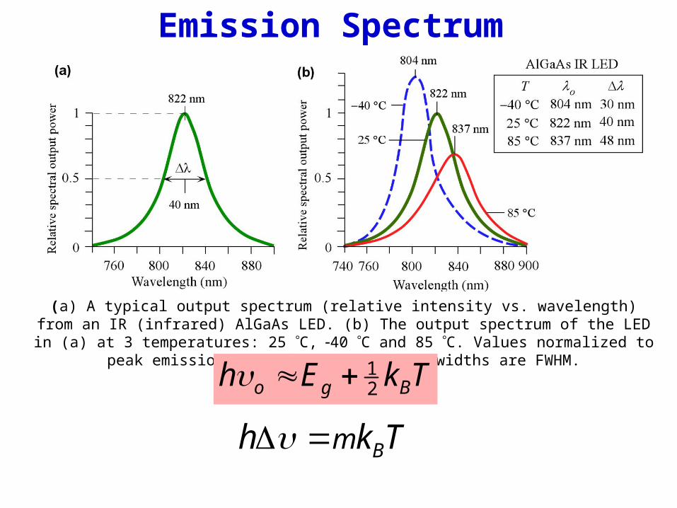
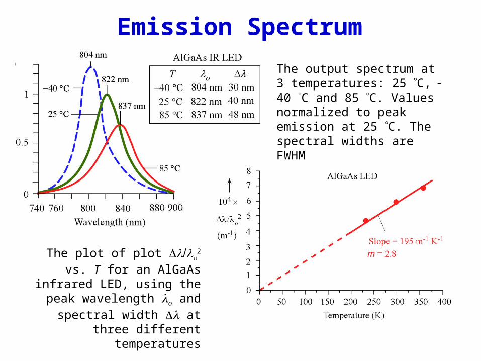
(a) A typical output spectrum (relative intensity vs. wavelength) from an IR (infrared) AlGaAs LED. (b) The output spectrum of the LED in (a) at 3 temperatures: 25 C, -40 C and 85 C. Values
normalized to peak emission at 25 C. The spectral widths are FWHM.
Emission Spectrum
The plot of plot Dl/lo2 vs. T for an AlGaAs infrared LED, using the peak wavelength lo and spectral
width Dl at three different temperatures
The output spectrum at 3 temperatures: 25 C, -40 C and 85 C. Values normalized to peak emission at 25 C. The spectral widths are FWHM
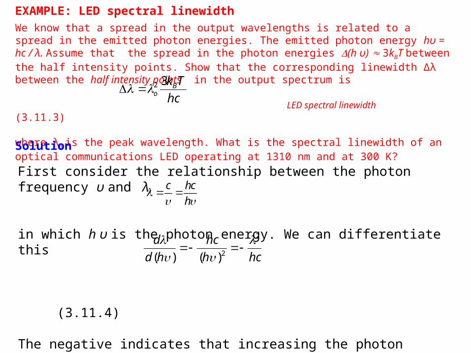
EXAMPLE: LED spectral linewidth
We know that a spread in the output wavelengths is related to a spread in the emitted photon energies. The emitted photon energy hυ = hc / λ. Assume that the spread in the photon energies (h υ) 3kBT between the half intensity points. Show that the corresponding linewidth Δλ between the half intensity points in the output spectrum is
LED spectral linewidth (3.11.3)
where λo is the peak wavelength. What is the spectral linewidth of an optical communications LED operating at 1310 nm and at 300 K?
First consider the relationship between the photon frequency υ and λ,
in which h υ is the photon energy. We can differentiate this
(3.11.4)
The negative indicates that increasing the photon energy decreases the wavelength. We are only interested in changes, thus Δ λ / Δ(hυ) |dλ /d(hυ)|, and this spread should be around λ = λo , so that Eq. (3.11.4) gives,
c hc
h
hch
hc
hd
d 2
2)()(
Solution
hc
TkBo
32