Embed Size (px)
Citation preview

JEDEC
PUBLICATION
FOUNDRY PROCESS
QUALIFICATION GUIDELINES –
FRONT END TRANSISTOR LEVEL
(Wafer Fabrication Manufacturing Sites)
JEP001-2A (Revision of JEP001A, February 2014)
SEPTEMBER 2018
JEDEC SOLID STATE TECHNOLOGY ASSOCIATION
Downloaded by xu yajun ([email protected]) on May 8, 2019, 11:21 pm PDT
beice
北测
(上
海)
电子
科技
有限
公司
联系方式:[email protected] 13917165676

NOTICE
JEDEC standards and publications contain material that has been prepared, reviewed, and
approved through the JEDEC Board of Directors level and subsequently reviewed and approved
by the JEDEC legal counsel.
JEDEC standards and publications are designed to serve the public interest through eliminating
misunderstandings between manufacturers and purchasers, facilitating interchangeability and
improvement of products, and assisting the purchaser in selecting and obtaining with minimum
delay the proper product for use by those other than JEDEC members, whether the standard is to
be used either domestically or internationally.
JEDEC standards and publications are adopted without regard to whether or not their adoption
may involve patents or articles, materials, or processes. By such action JEDEC does not assume
any liability to any patent owner, nor does it assume any obligation whatever to parties adopting
the JEDEC standards or publications.
The information included in JEDEC standards and publications represents a sound approach to
product specification and application, principally from the solid state device manufacturer
viewpoint. Within the JEDEC organization there are procedures whereby a JEDEC standard or
publication may be further processed and ultimately become an ANSI standard.
No claims to be in conformance with this standard may be made unless all requirements stated in
the standard are met.
Inquiries, comments, and suggestions relative to the content of this JEDEC standard or
publication should be addressed to JEDEC at the address below, or refer to www.jedec.org under
Standards and Documents for alternative contact information.
Published by
©JEDEC Solid State Technology Association 2018
3103 North 10th Street
Suite 240 South
Arlington, VA 22201-2107
This document may be downloaded free of charge; however JEDEC retains the
copyright on this material. By downloading this file the individual agrees not to
charge for or resell the resulting material.
PRICE: Contact JEDEC
Printed in the U.S.A.
All rights reserved
Downloaded by xu yajun ([email protected]) on May 8, 2019, 11:21 pm PDT
beice
北测
(上
海)
电子
科技
有限
公司
联系方式:[email protected] 13917165676

PLEASE!
DON’T VIOLATE
THE
LAW!
This document is copyrighted by JEDEC and may not be
reproduced without permission.
For information, contact:
JEDEC Solid State Technology Association
3103 North 10th Street
Suite 240 South
Arlington, VA 22201-2107
or refer to www.jedec.org under Standards-Documents/Copyright Information.
Downloaded by xu yajun ([email protected]) on May 8, 2019, 11:21 pm PDT
beice
北测
(上
海)
电子
科技
有限
公司
联系方式:[email protected] 13917165676

Downloaded by xu yajun ([email protected]) on May 8, 2019, 11:21 pm PDT
beice
北测
(上
海)
电子
科技
有限
公司
联系方式:[email protected] 13917165676

JEDEC Publication No. 001-2A
-i-
FOUNDRY PROCESS QUALIFICATION GUIDELINES – FRONT END TRANSISTOR LEVEL (Wafer Fabrication Manufacturing Sites)
Contents
Page Foreword i Introduction i Acronyms ii 1 Scope 1 2 Quality system 1 3 Responsibilities 1 3.1 Level 1 qualification 1 3.2 Level 2 qualification 2 4 Sample size 2 5 Use of packages 2 6 Reference documents 3 6.1 Industry standard documents 3 6.2 Selected references 4 7 Qualification test summary table 4 8 Conducting channel hot carrier injection (HCI) 5 8.1 DC conducting channel hot channel carrier (HCI) 5 9 Gate oxide integrity (GOI) 7 9.1 Voltage ramp dielectric breakdown (V-RAMP) & charge to breakdown (QBD) 7 9.2 Time-dependent dielectric breakdown (TDDB) 9 9.3 Plasma process-induced damage (P2ID) 11 10 Threshold voltage stability 13 10.2 Ionic contamination – bias temperature stress 13 10.3 Ionic contamination – triangular voltage sweep 14 10.4 Bias temperature instability in MOS devices (BTI) 15 11 Technology qualification vehicle (TQV) tests 17 11.1 Long term life test 17 11.2 Yield reporting 18 11.3 Report requirements 18 12 Process control monitor (PCM) characterization 18 12.1 PCM data 18 13 Construction analysis 22
Downloaded by xu yajun ([email protected]) on May 8, 2019, 11:21 pm PDT
beice
北测
(上
海)
电子
科技
有限
公司
联系方式:[email protected] 13917165676

JEDEC Publication No. 001-2A
-ii-
Foreword
The publication is divided into three parts, backend of line (JEP001-1A), transistor level (JEP001-2A), and product level testing (JEP001-3A). The document provides methodologies for the minimum set of measurements to qualify a new semiconductor wafer process. It is written with particular reference to a generic silicon based CMOS logic technology. While it may be applicable to other technologies (e.g., analog CMOS, bipolar, BICMOS, GaAs, etc.), some sections apply specifically to CMOS. No effort was made in the present document to cover all the qualification requirements for specific other technologies, e.g., Cu/Low K interconnects or ultra-thin gate oxide. Any qualification requirements beyond the minimum set are to be developed for the specific performance expected of the technology. The minimum set of measurements and the requirements for the qualification based on those measurements are to be determined between the foundry and its customers on an individual basis The process technology owner (foundry) will be required to document the details of specific testing unique to the process being qualified. The guideline documents common best practices in the semiconductor industry and updated in accordance to advancement in the semiconductor industry and JEDEC bylaws of periodic reviews.
Introduction
This publication, was originally published as JP-001 entitled 'Foundry Process Qualification Guidelines', it was co-sponsored by JEDEC and the FSA (Fabless Semiconductor Association). It originated at the FSA as a technology specific document, and has evolved into a generic set of qualification methodologies. The JEDEC sponsoring committee is JC-14 through its JC-14.2 subcommittee on wafer level reliability. This document encompasses and references a number of other standards and procedures, some of which are in a state of constant revision and update. While a case might be made for producing a lean, concise guideline that does not spell out specific procedures or requirements, the proposition of spelling out the essence of a comprehensive set of methodologies in one place has a practical value that outweighs the case for simplicity.(comment : the requirements are only spelled out in a number of cases. Best to be consistent and let the existing JEDEC specs speak for themselves)
This publication is split into three parts: JEP001-1A, JEP001-2A, and JEP001-3A as described below. It is intended that each part references the appropriate test and requirement noting that some tests may be performed on the package level. This standard should be read alongside reliability requirements established between the supplier and customer.
The structure of the JEDEC JEP001 series as currently conceived is as follows:
Part 1 – Backend of line testing Part 2 – Transistor-level testing Part 3 – Product-level testing
Downloaded by xu yajun ([email protected]) on May 8, 2019, 11:21 pm PDT
beice
北测
(上
海)
电子
科技
有限
公司
联系方式:[email protected] 13917165676

JEDEC Publication No. 001-2A
-iii-
Acronyms
The following acronyms have been used in this document. WLR: wafer level reliability IMD: inter/intra-metal dielectric HCI: hot carrier integrity GOI: gate oxide integrity VRDB: voltage ramp dielectric breakdown TDDB: time-dependent dielectric breakdown QBD: Charge to breakdown P2ID: plasma-process induced damage BTS: bias temperature stress TVS: triangular voltage sweep NBTI: negative bias temperature instability HTOL: high temperature operating life ESD: electrostatic discharge HBM: human body model MM: machine model CDM: charged device model TQV: technology qualification vehicle PCM: process control monitor FA: failure analysis .
Downloaded by xu yajun ([email protected]) on May 8, 2019, 11:21 pm PDT
beice
北测
(上
海)
电子
科技
有限
公司
联系方式:[email protected] 13917165676

JEDEC Publication No. 001-2A
-iv-
Downloaded by xu yajun ([email protected]) on May 8, 2019, 11:21 pm PDT
beice
北测
(上
海)
电子
科技
有限
公司
联系方式:[email protected] 13917165676

JEDEC Publication No. 001-2A Page 1
FOUNDRY PROCESS QUALIFICATION GUIDELINES - FRONT END TRANSISTOR LEVEL (Wafer Fabrication Manufacturing Sites)
(From JEDEC Board Ballot JCB-18-15, formulated under the co-sponsorship of the JC-14.2 Subcommittee on Wafer Level Reliability.)
1 Scope
This document describes transistor-level test and data methods for the qualification of semiconductor technologies. It does not give pass or fail values or recommend specific test equipment, test structures or test algorithms. Wherever possible, it references applicable JEDEC such as JESD47 or other widely accepted standards for requirements documentation. There are two levels of qualification described. Level 1 is a pure process qualification intended to find reliability weaknesses. It primarily addresses technology wearout mechanisms through package or wafer level reliability tests on specially designed test structures. Level 2 demonstrates the reliability of the process that corresponds to the reliability demands from projected or known applications. Level 2 testing can be implemented via the testing of a relevant functional technology qualification vehicle (TQV), including life test. The level 2 tests are described in Section 12. Other Reporting requirements (e.g., PCM data) are also included.
2 Quality system
It is the responsibility of the foundry to have the appropriate quality system in place with special emphasis on issues relating to equipment capability, maintenance and calibration, continuous improvement and process control. In particular, a functioning SPC methodology should be demonstrated for all key processes (see EIA/JEDEC EIA-557A). As a minimum the foundry will have ISO9001 certification. The ISO9001 audit results by a third party and subsequent corrective actions on deficiencies shall be made available to the customer upon request. For those supplying to automotive applications, the foundry may also have to demonstrate requirements from the IATF TS 16949 standard to meet the needs of these products.
3 Responsibilities
3.1 Level 1 qualification The foundry is responsible for the design and implementation of the level 1 test vehicle (i.e., TESTCHIP). For the special case of a foundry customer driving process development, development of the level 1 test vehicle may be shouldered in whole or in part by the customer. The foundry shall fabricate the qualification silicon, execute the described level 1 tests and create the qualification report. The tests and qualification report may be done by the foundry or third party test vendor. The qualification requirements may be reduced for a derivative process, where the parent process has already been fully qualified at the same location.
Downloaded by xu yajun ([email protected]) on May 8, 2019, 11:21 pm PDT
beice
北测
(上
海)
电子
科技
有限
公司
联系方式:[email protected] 13917165676

JEDEC Publication No. 001-2A Page 2
3.2 Level 2 qualification In general, the foundry is responsible for the design and implementation of the Level 2 test vehicle (e.g., SRAM or pilot product). For the special case of a foundry customer driving process development, or where the customer requires TQV data before such a vehicle becomes available, development of the level 2 test vehicle may be shouldered in whole or in part by the customer. The foundry, customer or third party test vendor may execute the Level 2 (TQV) tests and requisite failure analysis. The foundry will be responsible for suggesting and implementing corrective action based on the failure analysis results. The qualification report shall adhere to the minimum reporting requirements and format described in this document.
While it is expected that a particular foundry methodology may differ from the methods outlined in this document, the wafer foundry should demonstrate to the customer that it has satisfactorily addressed all issues of interest. The wafer foundry should therefore provide a documented procedure and supporting data that provide an assessment of potential failure and wearout mechanisms.
3.3 Reporting Requirements
Specific reporting requirements are included for the tests catalogued in this document. General reporting requirements include appropriate signoff, archiving and revision control, and the inclusion of supporting documents as appropriate.
The level 1 qualification report shall include: (1) qualification plan, (2) description of the test vehicle including relevant test structure features and dimensions, (3) summary of test methods used, (4) pass/fail criteria and (5) test results, analysis and model parameters as described in this document.
The level 2 qualification report shall include: (1) qualification plan, (2) description of the technology qualification vehicle (TQV), (3) test description & specification, (4) pass/fail criteria (5) test results & analysis including failure rates and (6) FA results.
4 Sample size
In general, data should come from 3 non-consecutive wafer lots, although the use of more lots is not precluded. A wafer lot is a group of wafers processed as a batch through the same or matched equipment in the same processing interval, using the same or matched conditions, materials, and methods. Typical sample sizes per lot are given in the individual test descriptions. Where applicable, confidence limits for each test population should be calculated. A conservative estimate of 40 die per wafer was made in determining sample size for tests that required the usage of all dies on the wafer.
5 Use of packages
Packages with a wire-bonded die that are capable of higher temperatures are generally used for testing of the technology qualification vehicle (TQV) or pilot product. A qualification report for the standard wire-bonding process should be included. Advanced packaging (e.g., BGA, flip-chip or chip-scale) may be substituted where applicable. This, in combination with TC and THB tests will demonstrate the assembly capability of this wafer fab process.
Side brazed ceramic packages are generally required for process wear-out tests performed at package-
level at Temperatures greater than 155C. Consequently, wafer level testing is recommended wherever possible.
All references to temperature in the following sections imply junction temperature unless otherwise specified.
Downloaded by xu yajun ([email protected]) on May 8, 2019, 11:21 pm PDT
beice
北测
(上
海)
电子
科技
有限
公司
联系方式:[email protected] 13917165676

JEDEC Publication No. 001-2A Page 3
6 Reference documents
6.1 Industry standard documents The following reference documents contain provisions that, through reference in this text, constitute provisions of this document. For dated references, subsequent amendments to, or revisions of, any of these publications do not apply. However, parties to agreements based in this publication are encouraged to investigate the possibility of applying the most recent editions of the reference documents indicated below. For undated references, the latest editions of the reference document referred to applies. Check the JEDEC website at http://www.jedec.org.
6.1.1 Reliability assessment methodology JEDEC JEP70, Quality and Reliability Standards and Publications.
JEDEC JEP132, Process Characterization Guidelines.
JEDEC JEP143, Solid State Reliability Assessment and Qualification Methodologies.
JEDEC JEP122, Failure Mechanisms and Models for Silicon Semiconductor Devices.
JEDEC JESD91, Method for Developing Acceleration Models for Electronic Component Failure Mechanisms.
JEDEC JESD94, Application Specific Qualification Using Knowledge Based Test Methodology.
JEDEC JESD659, Failure-Mechanism-Driven Reliability Monitoring.
JEDEC JEP131, Process Failure Mode and Effects Analysis (FMEA). 6.1.2 Hot carrier integrity JEDEC JESD28, A Procedure for Measuring N-Channel MOSFET Hot-Carrier-Induced Degradation under DC Stress. See also EIA/JEDEC JESD28-1 (addendum on data analysis).
JEDEC JESD60, A Procedure for Measuring P-Channel MOSFET Hot-Carrier-Induced Degradation under DC Stress. See also JEDEC JESD60-1 (Addendum on data analysis). 6.1.3 Bias Temperature Instabilities JEDEC JESD241, Procedure for wafer-level DC characterization of bias temperature instabilities 6.1.4 Gate oxide integrity JEDEC JESD35A, Procedure for Wafer-Level-Testing of Thin Dielectrics. See also addendum’s JESD35-1 (test structures) and JESD35-2 (test criteria). JESD92, Procedure for Characterizing Time-Dependent Dielectric Breakdown of Ultra-Thin Gate Dielectrics. 6.1.5 E-Test Parameters ASTM F616-86, Standard Test Method for Measuring MOSFET Drain Leakage Current.
ASTM F617-86, Standard Test Method for Measuring MOSFET Linear Threshold Voltage.
ASTM F1096-87, Standard Test Method for Measuring MOSFET Saturated Threshold Voltage.
Downloaded by xu yajun ([email protected]) on May 8, 2019, 11:21 pm PDT
beice
北测
(上
海)
电子
科技
有限
公司
联系方式:[email protected] 13917165676
JEDEC Publication No. 001-2A Page 4
6.2 Selected references Meeker, Q.A. and L.A. Escobar, Statistical Methods for Reliability Data, John Wiley, 1998. Tobias, P.A. and D.C. Trindade, Applied Reliability, 2
nd Ed., CRC Press, 1995.
Nelson, Wayne, “Accelerated Testing: Statistical Models, Test Plans, and Data Analyses”, in Wiley Series in Probability and Mathematical Statistics-Applied Probability, John Wiley, 1990. Amerasekera, E.A. and F.N. Najm, Failure Mechanisms in Semiconductor Devices, 2
nd Ed., John Wiley,
1997. Ohring, Milton, Reliability and Failure of Electronic Materials and Devices, Academic Press, 1998. Yue, John, “Reliability”, in C.Y. Chang and S.M. Sze (eds.), ULSI Technology, McGraw-Hill, 1996, Chapter 12. Takeda, E. et al, Hot-Carrier Effects in MOS Device, Academic Press, 1995. Amerasekera, E.A. and Charvaka Duvvury, ESD in Silicon Integrated Circuits, John Wiley, 1996. IRPS Conference Proceedings and Tutorials are an excellent source of information on current test methodologies and reliability models. (Web site www.irps.org) Microelectronics Reliability, Pergamon Press. This journal publishes the proceedings of ESREF, the European equivalent of IRPS, along with frequent review papers. Abadeer, W.W., IEEE Transactions on Device and Materials Reliability, Vol. 1, No. 1, March 2001, Reliability Monitoring and Screening Issues With Ultrathin Gate Dielectric Devices.
Downloaded by xu yajun ([email protected]) on May 8, 2019, 11:21 pm PDT
beice
北测
(上
海)
电子
科技
有限
公司
联系方式:[email protected] 13917165676

JEDEC Publication No. 001-2A Page 5
7 Qualification test summary table
Clause Procedure JEDEC Reference
Standard(s) Other Standards
Qual or Eng
8.1 DC Hot Carrier Injection JESD28, JESD60, JEP122 EIAJ-987 Q
9.1 Voltage Ramp Dielectric Breakdown (VRDB) / Charge to Breakdown (QBD)
JESD35 Q
9.2 Time-Dependent Dielectric Breakdown (TDDB)
JESD92, JEP122 EIAJ-988 Q
9.3 Plasma Process Induced Damage (P2ID) None Q or E
10.1 Ionic Contamination/ Bias Temperature Stress (BTS)
None Q or E
10.2/3 Ionic Contamination/ Triangular Voltage Sweep (TVS)
None Q or E
10.4 Bias Temperature Instability (BTI) JESD241, JEP122 Q
8 Conducting channel hot carrier injection (HCI)
8.1 DC conducting channel hot carrier (HCI)
1. Testing should be done on the minimum geometry device for each transistor type (NMOS, PMOS, native or low VT device, etc.). Additional device lengths may be tested for modeling purposes.
2. The degradation should be evaluated at the worst case bias conditions (refer to JEDEC procedures).
3. The failure criteria for the monitored parameters will depend on the specific requirements of the technology.
4. The lifetime calculated from this stress reflects operation at worst case dc bias. Use conditions may be ac. Product lifetime will depend on use of device in circuit, and ac stress testing and/or simulation is highly recommended.
Downloaded by xu yajun ([email protected]) on May 8, 2019, 11:21 pm PDT
beice
北测
(上
海)
电子
科技
有限
公司
联系方式:[email protected] 13917165676

JEDEC Publication No. 001-2A Page 6
8.1.1 DC HCI test requirements
Reference Procedures
JESD60, JESD28, JEP122, and JESD28-1
Test parameters & failure criteria
a) A DUT is considered to fail when a chosen device parameter changes by more than the specified failure criterion (typically 10% change in device parameter) at worst use condition (typically VDDMAX = 1.1VDD) at a specified end of life. Example of a typical failure criterion is 10% change in forward IDSAT.
b) Selection of devirameter depends on the impact of the shift in its value on circuit operation.
c) Device parameters such as IDSAT, GM, IDLIN, VTLIN, IOFF can be used to monitor HC degradation
depending on the circuit application.
Test structures BOTH NMOSFET / PMOSFET: Minimum and nominal channel length L (W if required) as allowed by the circuit design rules. All Voltage Supply Device options offered must be evaluated. See JESD28 and JESD60 for requirements.
Vehicle Wafer Level or Packaged Level
Method Stress Temperature: While the activation energy for HCI is generally small and can be either positive or negative, it is recommended that the activation energy be determined over the full range of expected product operation. Project to EOL conditions using this activation energy The device
junction temperature should be held to an accuracy of 2 C for the duration of stress/test. See JESD28 and JESD60.
Drain-Source Voltage @ stress: Test at 3-5 different VDS stress conditions
Gate-Source Voltaqe @ stress: Determine worst-case VGS taking operating conditions into account. (This can be at Peak ISUB or VGS = VDS or VGS = VDD / 2 for NMOSFET and PMOSFET devices, see JESD28, JESD60 & JEP122).
NOTE: If these gate stresses are not suitable per intended application, then preliminary stress tests should be
implemented to characterize and identify allowable worst gate stress condition. Also, short and long channels should be considered to identify allowable worst gate stress condition.
Readouts: Log time scale with minimum two log-time intervals per decade (at least 2 points per decade.)
Model to be used 1/VDS model applies if HCI is worst at lower temperature, different VDS model e.g., exponential or power-law as demonstrated by the data applies if HCI is worst at higher temperature. Must characterize VGS/VDS dependence to find worst case, with 3-5 VGS/VDS as typical conditions).
Sample size Required
a) Test nominal devices from 3 lots, 3 wafers per lot, 5 sites minimum per bias condition, at 3-5 VDS stress conditions and 3-5 VGS.
Additional (not gating qualification)
b) Test nominal devices from > 10 lots with different manufacturing dates. Test 10 sites per wafer at one VDS stress condition and for a given LEFF. Short In line HC stresses at worst case condition can be run to provide the statistics. The resulting distribution is a measure of the HC sensitivity to intrinsic process tolerances.
NOTE 1 Process Corners: The hot carrier lifetime may vary widely across a typical process window. It is a sensitive function of gate length. For this reason, extraction of hot carrier lifetime for the nominal device can yield an optimistic result. It is therefore recommended to include in the evaluation test samples that give a measure of performance near the process corners.
NOTE 2 Data collected in part (b) is intended as supplemental data, to be collected over time, at the same time that product yield data is collected. This is not necessarily a qualification gating item.
Merit number Lifetime projection at temperature and voltage conditions appropriate for the application. BTI shift should be decoupled from HCI shift by, for example, comparing high and low temperature shift.
Downloaded by xu yajun ([email protected]) on May 8, 2019, 11:21 pm PDT
beice
北测
(上
海)
电子
科技
有限
公司
联系方式:[email protected] 13917165676

JEDEC Publication No. 001-2A Page 7
8.1.2 Report requirements
These guidelines should not replace any existing agreements between customers and suppliers regarding specific information for reporting purposes.
1) Fab name and location; process name, lot #, wafer # and date code, and certification that material tested represents the current process being qualified.
2) General process features may include: device isolation scheme (LOCOS, STI), oxide thickness, minimum drawn device lengths and widths, minimum electrical LEFF, source and drain engineering, sidewall/spacer process.
3) Relevant spec limits: Effective channel length and width, drain current, threshold voltage, substrate current, Gate current, Channel off current, overlap capacitance.
4) Description of test structures and test conditions (VDS & VGS) for each transistor type.
5) Sample size for each stress condition.
6) Failure criterion and parameters selected to monitor HC degradation.
7) Measured parameter ranges: drain current, substrate current, etc.
8) Acceleration models used and extracted parameters for these models.
9) Extracted parameters for the specific hot carrier degradation model used.
10) Lognormal sigma of the HC shifts from collected data.
11) Decoupling of BTI shift from HCI shift should be shown.
Downloaded by xu yajun ([email protected]) on May 8, 2019, 11:21 pm PDT
beice
北测
(上
海)
电子
科技
有限
公司
联系方式:[email protected] 13917165676

JEDEC Publication No. 001-2A Page 8
9 Gate oxide integrity (GOI)
9.1 Voltage ramp dielectric breakdown (V-RAMP) & charge to breakdown (QBD)
1. Follow the V-RAMP test procedure described in JEDEC standard JESD35-A. - Test is done in accumulation or inversion mode, at room temperature.
- Test is done at wafer level.
- Start voltage is VUSE.
- Typical ramp rate: 1MV/cm-s; Setup duration: 0.1s (please note that ramp rate is a variable that should represent test objective and design features)
- Breakdown is defined as a change in current density between successive voltage steps.
- Post-breakdown test is done at VUSE. 2. The primary purpose of this test is to evaluate the extrinsic behavior of the MOS gate oxide being
qualified. 3. The V-RAMP test is usually done in accumulation. Testing in inversion is also recommended.
However, care should be taken to avoid difficulties caused by certain structures, if there is no low resistance current path to the substrate.
4. The V-RAMP test should be done on both NMOS and PMOS capacitors, for every type of oxide in the
technology.
5. The preferred test structure is a capacitor array dimensionally representative of product (e.g., transistor array). Variously, a combination of at least three different geometry devices may be tested: isolation Edge Block (Area), Isolation Edge Finger (trench or FOX edge) and Gate Edge Finger.
6. The procedure of detection and analysis of gate dielectric defects is given by JESD35-A Annex A.
The sample requirement to demonstrate a given target defect density may be determined by using the formula below (see JESD35-A), where N is the total sample size, ATEST is the gate area per test structure and D0 is the target defect density:
N*ATEST > -ln (1-0.95)/D0
7. Distributions, not averages should be quoted. 8. The charge to breakdown (QBD) may be calculated by integrating the current density through the
capacitor until the last point before breakdown. Care should be exercised in interpreting QBD, particularly for thin oxides, where there is weak correlation to oxide quality, and where QBD is a function of stress voltage.
Downloaded by xu yajun ([email protected]) on May 8, 2019, 11:21 pm PDT
beice
北测
(上
海)
电子
科技
有限
公司
联系方式:[email protected] 13917165676
JEDEC Publication No. 001-2A Page 9
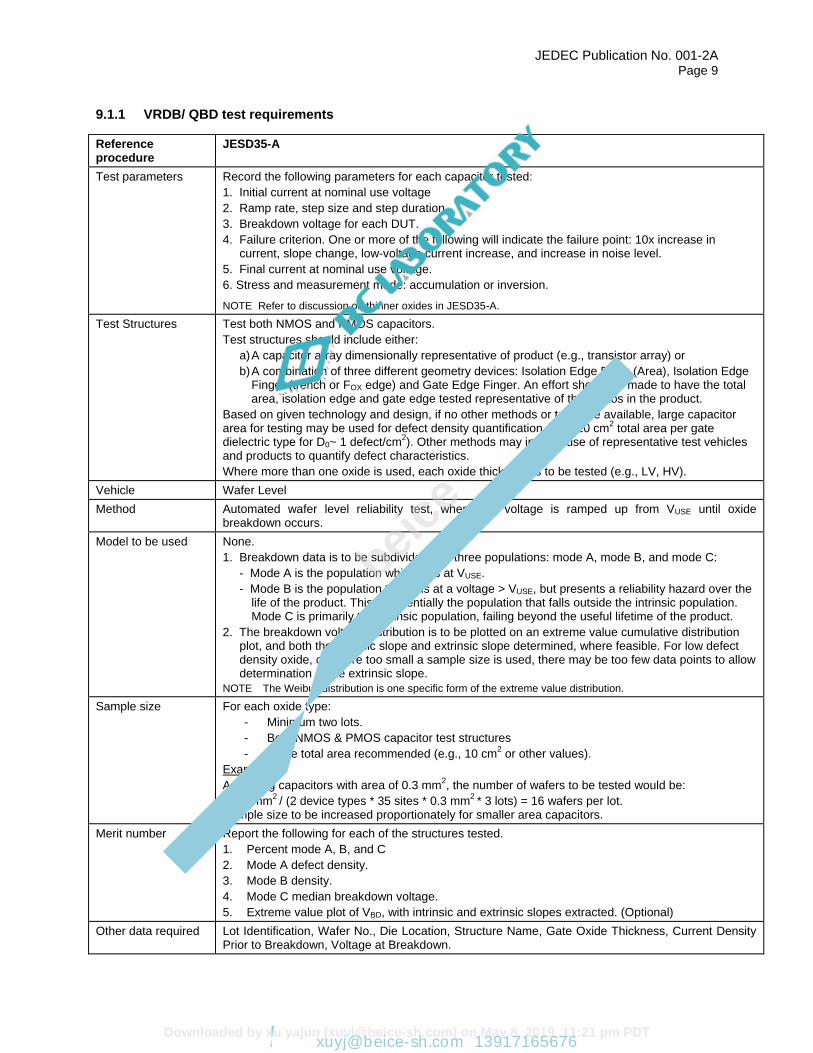
9.1.1 VRDB/ QBD test requirements
Reference procedure
JESD35-A
Test parameters Record the following parameters for each capacitor tested:
1. Initial current at nominal use voltage
2. Ramp rate, step size and step duration.
3. Breakdown voltage for each DUT.
4. Failure criterion. One or more of the following will indicate the failure point: 10x increase in current, slope change, low-voltage current increase, and increase in noise level.
5. Final current at nominal use voltage.
6. Stress and measurement mode: accumulation or inversion.
NOTE Refer to discussion on thinner oxides in JESD35-A.
Test Structures
Test both NMOS and PMOS capacitors.
Test structures should include either:
a) A capacitor array dimensionally representative of product (e.g., transistor array) or
b) A combination of three different geometry devices: Isolation Edge Block (Area), Isolation Edge Finger (trench or FOX edge) and Gate Edge Finger. An effort should be made to have the total area, isolation edge and gate edge tested representative of their ratios in the product.
Based on given technology and design, if no other methods or tools are available, large capacitor area for testing may be used for defect density quantification (e.g., 10 cm
2 total area per gate
dielectric type for D0~ 1 defect/cm2). Other methods may include use of representative test vehicles
and products to quantify defect characteristics.
Where more than one oxide is used, each oxide thickness is to be tested (e.g., LV, HV).
Vehicle Wafer Level
Method Automated wafer level reliability test, where the voltage is ramped up from VUSE until oxide breakdown occurs.
Model to be used None.
1. Breakdown data is to be subdivided into three populations: mode A, mode B, and mode C:
- Mode A is the population which fails at VUSE.
- Mode B is the population that fails at a voltage > VUSE, but presents a reliability hazard over the life of the product. This is essentially the population that falls outside the intrinsic population. Mode C is primarily the intrinsic population, failing beyond the useful lifetime of the product.
2. The breakdown voltage distribution is to be plotted on an extreme value cumulative distribution plot, and both the intrinsic slope and extrinsic slope determined, where feasible. For low defect density oxide, or where too small a sample size is used, there may be too few data points to allow determination of the extrinsic slope.
NOTE The Weibull distribution is one specific form of the extreme value distribution.
Sample size For each oxide type:
- Minimum two lots.
- Both NMOS & PMOS capacitor test structures
- Large total area recommended (e.g., 10 cm2 or other values).
Example:
Assuming capacitors with area of 0.3 mm2, the number of wafers to be tested would be:
1000 mm2
/ (2 device types * 35 sites * 0.3 mm2
* 3 lots) = 16 wafers per lot. Sample size to be increased proportionately for smaller area capacitors.
Merit number Report the following for each of the structures tested.
1. Percent mode A, B, and C
2. Mode A defect density.
3. Mode B density.
4. Mode C median breakdown voltage.
5. Extreme value plot of VBD, with intrinsic and extrinsic slopes extracted. (Optional)
Other data required Lot Identification, Wafer No., Die Location, Structure Name, Gate Oxide Thickness, Current Density Prior to Breakdown, Voltage at Breakdown.
Downloaded by xu yajun ([email protected]) on May 8, 2019, 11:21 pm PDT
beice
北测
(上
海)
电子
科技
有限
公司
联系方式:[email protected] 13917165676

JEDEC Publication No. 001-2A Page 10
9.1.2 Report requirements
These guidelines should not replace any existing agreements between customers and suppliers regarding specific information for reporting purposes.
1. Fab name and location; process name, lot #, wafer # and date code, and certification that material tested represents the current process being qualified.
2. Relevant process features: device isolation scheme (LOCOS, STI), oxide thickness.
3. Brief description of test structures (device type, gate area, poly edge, FOX edge)
4. Brief description of test conditions (temperature, polarity, stress voltage, fail limits)
5. Sample size for each stress condition.
6. Measured parameters from oxide characterization: ellipsometry, I-V, C-V, QM analysis.
NOTE Ellipsometry may be replaced by other electrical measurements for thin gate oxide (e.g., < 5nm, per JESD90)
7. Measured initial leakage at VUSE. Data should be presented in an extreme value plot or similar format. Where leakage data includes values > 10X the media value, a wafer map representation may be required.
8. Extracted parameters from extreme value plot: Median breakdown voltage, intrinsic slope, extrinsic slope (if sufficient data).
9. Report the following:
a. Percent mode A, B & C for each structure and lot tested.
b. Mode A and mode B defect densities.
c. Mode C breakdown voltage (T63)
d. Optional: Extreme value plots and distribution parameters. 9.2 Time-dependent dielectric breakdown (TDDB)
1. The TDDB test is used to model the intrinsic behavior in the technology being qualified using temperature and voltage acceleration.
2. The time to fail (tBD) scales inversely with voltage, temperature and the oxide area being tested.
3. At least three defect generation mechanisms have been identified in the breakdown of gate dielectrics: Impact ionization and anode hole-injection at higher voltages, and trap creation at operating voltages.
4. Current evidence points to a critical defect density (NBD
) which may be voltage and time dependent.
5. The statistics of gate oxide breakdown are described by the Weibull distribution, which is defined by the characteristic life, t63, and the Weibull slope,
F(t) = 1 – exp [-(t / t63)].
6. For thinner oxides, the first breakdown – whether soft or hard (see note) - should be used in the statistical distribution.
NOTE the distinction between soft and hard breakdown is based on the post-breakdown behavior of the test structure, which depends in large measure on the energy dissipated in the filamentary short. Hard breakdown results in a resistive short (several orders increase in current). By contrast, soft breakdown results in a non-zero resistive path (a few-fold increase in current).
7. Where a field dependence model is appropriate, it is important to model the oxide thickness and oxide field accurately.
Downloaded by xu yajun ([email protected]) on May 8, 2019, 11:21 pm PDT
beice
北测
(上
海)
电子
科技
有限
公司
联系方式:[email protected] 13917165676

JEDEC Publication No. 001-2A Page 11
9.2.1 TDDB test requirements
Reference procedure
JESD92
Test parameters Record the following parameters for each capacitor tested:
1. Initial current at nominal use voltage
2. Initial current at start of stress.
3. Failure time for each DUT. Fit data for each stress condition on a Weibull plot to obtain t63 and
the Weibull slope ().
4. Final current at nominal use voltage. (Optional)
Failure criterion Any of several failure criteria may be used, e.g., increase in current, increase in current at use voltage or lower, increase in stress current, increase in stress current noise.
Test structures
a) Test NMOS and PMOS capacitors, preferably transistor arrays reflecting actual circuit topographies.
b) Optional: It is suggested that 2 capacitors of similar layout but very different areas be tested.
For specific test structure criteria, see JEDEC standard JESD35.
Vehicle Package or Wafer Level
Method 1. Constant voltage stress (CVS) at various stress voltages and temperatures.
2. Preferably, test should be done both in accumulation and inversion. As a minimum, accumulation test data should be provided.
3. Voltage acceleration: Use > 3 voltages above VG > VDDMAX.
4. Temperature acceleration (optional): Use at least 3 temperatures in the range of 25-200 C.
5. If only one temperature is used, stressing at the maximum operating temperature is recommended to avoid using temperature acceleration.
6. Stress until at least 63% of the samples have failed.
Model to be used Use an appropriate model to extrapolate to use conditions for the actual product die: for details see JEP122 section 5.1.
Sample size Minimum one capacitor with representative topography for each device type (NMOS & PMOS) and oxide thickness
Minimum 2 lots
Minimum 2 wafers per lot
Minimum 8 DUTs per wafer for every stress condition (voltage and temperature combination)
Minimum 30 DUT per single distribution, for ultra-thin oxides > 50 DUT is recommended
Example (3 voltages @ 1 temperature): 1 array capacitor * 2 device types * 3 voltages * 8 DUTs * 2 wafers * 2 lots = 192 DUTs
NOTE Sample size should be increased for thinner oxide, since the Weibull slope is known to decrease with decreasing thickness.
Merit number Depends on application
Other data required Lot Identification, Wafer No., Die Location, Structure Name, Gate Oxide Thickness by optical and/or electric methods, Current Density Prior to Breakdown.
Downloaded by xu yajun ([email protected]) on May 8, 2019, 11:21 pm PDT
beice
北测
(上
海)
电子
科技
有限
公司
联系方式:[email protected] 13917165676

JEDEC Publication No. 001-2A Page 12
9.2.2 Report requirements
These guidelines should not replace any existing agreements between customers and suppliers regarding specific information for reporting purposes.
1. Fab name and location; process name, lot #, wafer # and date code, and certification that material tested represents the current process being qualified.
2. Relevant process features: device isolation scheme (LOCOS, STI), oxide thickness
3. Brief description of test structures (device type, area, poly edge, FOX edge)
4. Brief description of test conditions (temperature, polarity, stress voltage, fail limits)
5. Sample size for each stress condition.
6. Measured parameters from oxide characterization: Ellipsometry, I-V, C-V.
NOTE Ellipsometry may be replaced by other electrical measurements for thin gate oxide
7. Measured parameters from TDDB stress: Initial current density, time to breakdown, final current density
8. Extracted parameters from Weibull plot: characteristic life t63, Weibull slope,.
9. Extracted parameters for oxide degradation model, e.g., Voltage acceleration factor, activation energy EA.
10. Projected lifetime at maximum use conditions.
11. Optional: Construct a 90% confidence interval about the projected lifetime distribution produced in item 10 above. Compare this confidence interval to the qualification pass criteria, to judge the risk that repeating the qualification will result in a fail outcome.
9.3 Plasma process-induced damage (P2ID) 1. The primary goal of this test is to confirm that the P2ID design rules are achievable by the process.
2. This test may be done as part of the qualification, or as an engineering study
3. This test is to be done on MOS transistors.
4. In many cases, it is essential to apply a stress to reveal latent damage.
5. Fowler-Northeim (F-N), hot carrier stress (HC), conducting and non-conducting and Negative bias temperature instability (NBTI) stress may be used to reveal latent damage. Characterization is recommended to understand sensitivity to stress conditions
6. The effect of P2ID is reflected by the distributions before and after stress, between reference and antenna structures, of one or more of the following parameters: Threshold voltage (VT), transconductance (GM), drain saturation current (IDSAT), drain off current (IDOFF) and gate leakage at low voltage (ILEAK).
7. Elapsed time considerations must not be ignored. Plasma damage may be present, with adverse effect on device reliability, even if yield at t = 0 is not.
8. Voltage ramp breakdown, QBD and TDDB tests have been used to monitor possible P2ID damage. However, the sensitivity of a given test or structure appears to vary with oxide thickness.
9. For thinner oxides ( 5nm), weaker parametric shifts, or no shifts at all, may be observed for a given applied stress. Initial ILEAK at voltages which may show some tunneling current has been reported to be a sensitive indicator of damage. However, care should be exercised in the selection of test structures and the interpretation of data.
Downloaded by xu yajun ([email protected]) on May 8, 2019, 11:21 pm PDT
beice
北测
(上
海)
电子
科技
有限
公司
联系方式:[email protected] 13917165676

JEDEC Publication No. 001-2A Page 13
9.3.1 P2ID test requirements
Reference procedure
1. C.R. Viswanathan, 1997 Int’l Symposium on P2ID, pp. 181-185
2. K. P. Cheung, IRPS 1997 Tutorial Notes Topic 4
3. T. Hook et al, 1996 Int’l Symposium on P2ID, pp. 164-167.
4. A. Sridharan et al, 1997 P2ID, pp. 29-32.
5. K. P. Cheung et al, 2000 Int’l Symposium on P2ID, pp. 10-13.
6. A.Martin et al., IEEE TDMR, vol.9, no.2, pp.135-144, 2009.
Test parameters Wafer map distributions of reference and worst case antenna device parameters: VT, GM, IDSAT, IDOFF, and ILEAK, before and after FN, HC or NBTI stress. The failure criterion is one of the following:
Parameter value is outside a defined spec. limit
Parameter difference for reference and antenna device exceeds a defined percentage limit
Parameter shift exceeds a defined percentage limit.
Parameter spatial variation exceeds a defined percentage limit
The selected parameter(s) and defined pass/fail limits are to be demonstrated to be appropriate for the specific process.
Test structures Structure should be designed for allowable worst case setting considering (L&W) geometric constraints (min. L & wide W) for N & P MOSFET devices for each gate oxide thickness.
Comparison between reference and antenna devices should be carried out on the same identical geometry and same die.
The following structures of each type are to be tested:
- Reference device: protected from plasma damage.
- Devices with worst case antenna ratios for each process layer: poly, contact, metal1, etc.
- Reference and antenna device must be connected to the probing pads in an identical way.
Vehicle Wafer level measurements at room temperature (except for NBTI at higher temperatures)
Method Identical steps should be applied to reference and antenna devices:
1. Measure parameter values across wafer. Parameters to be measured to include one or more of the following: VT, GM, S, IDSAT and IDOFF.
NOTE Gate leakage current should be measured at low voltage (~1V) (for HCS or BTI): gate to bulk and gate to source/drain.
2. Apply stress to reveal damage using one of the following:
a) FN Stress (gate injection in inversion). Optimum stress level to be determined for the specific process. The stress level should be sufficient to repopulate existing traps without adding excessive new damage (e.g., 10 mA/cm
2 for 10 sec – number of merit is an injected charge of
0.1C/ cm2 ).
b) HC or NBTI stress. Stress at room temperature for conducting hot carrier, and at maximum temperature of operation (or burn-in) for NBTI or non-conducting hot carrier. Optimum stress level to be determined experimentally for the specific process.
3. Re-measure parameter values across wafer.
4. Map parameter shift across wafer.
CAUTION A finite charging time may be associated with FN stress or gate leakage measurements on test structures with large antenna ratio, due to the high capacitance. This may lead to an overestimation of applied stress or gate leakage current.
Model to be used None
Sample size Suggested: 180 (20 Die * 3 Wafers * 3 Lots) This should be uniformly spaced across the wafer.
Merit number Transistor device parameters:
Percent Variation across wafer, wafer to wafer and lot to lot.
Percent difference between reference and antenna structures on the measured devices, Percent shift pre and post stress.
Include wafer maps of the above distributions
NOTE Variations and differences can be evaluated from a cumulative distribution instead of die to die basis (or unit, sample level)
Other data required
Lot Identification; wafer number; die Location; gate Oxide Thickness; Other details such as transistor/capacitor geometry and of antenna layout (finger or area, contact array, etc.) may depend on existing supplier and customer agreements.
Downloaded by xu yajun ([email protected]) on May 8, 2019, 11:21 pm PDT
beice
北测
(上
海)
电子
科技
有限
公司
联系方式:[email protected] 13917165676

JEDEC Publication No. 001-2A Page 14
9.3.2 Report requirements
These guidelines should not replace any existing agreements between customers and suppliers regarding specific information for reporting purposes.
1) Fab name and location; process name, lot number, wafer number and date code, and certification that material tested represents the current process being qualified. Describe protection scheme (e.g., MOS transistor
2) Relevant process features: device isolation scheme (LOCOS, STI), oxide thickness, minimum drawn device lengths, minimum LEFF.
3) Relevant spec limits: effective channel length, drain current, threshold voltage, and substrate current, off current.
4) Brief description of test structures and test conditions. Description of antenna ratios is also recommended.
5) Sample size per lot for each measurement.
6) Median value and standard deviation for each distribution of measured and calculated parameters for reference and antenna device before and after stress: Leakage current, threshold voltage, drain current and deltas.
7) Wafer maps for each measured/calculated parameter before and after stress.
10 Threshold voltage stability
NOTE With advanced nodes driving towards thinner gate oxide, the values for Threshold Voltage Stability tests described in this section may become limited or unfeasible. Therefore they may be replaced by other test methods in accordance to the supplier’s designs and capabilities or other available references.
10.1 Ionic contamination – bias temperature stress This test may be done as part of the qualification, or as an engineering study. The primary goal is to confirm that the ionic contamination level introduced into the process wafers does not adversely affect the reliability or parametric control of the process. NOTE Either the Bias Temperature Stress (BTS) (see 11.1) or the Triangular Voltage Sweep (TVS) (see 11.2) may be used or the results reported as shown below. Demonstrate no measurable ionic contamination.
Downloaded by xu yajun ([email protected]) on May 8, 2019, 11:21 pm PDT
beice
北测
(上
海)
电子
科技
有限
公司
联系方式:[email protected] 13917165676

JEDEC Publication No. 001-2A Page 15
10.1.1 Bias temperature stress (BTS) test requirements
Reference procedure None. Abadeer, W.W., IEEE Transactions on Device and Materials Reliability, Vol. 1, No. 1, March 2001, Reliability Monitoring and Screening Issues With Ultrathin Gate Dielectric
Devices.
Test parameters Threshold voltage shifts on parasitic (field) or gate oxide devices
Test structures NMOS and PMOS transistor structures, with or without self-heating, processed to final metal.
Design without the protection diode. Add metal gate field oxide parasitic test structure, (such as N-well to N-well source-drain with field ox as gate of parasitic MOS).
Vehicle Wafer or packaged device.
Method Heat up device to > 200 C, apply +0.1-0.5 MV/cm field between gate and bulk, source and drain.
The inversion the channel needs higher field. , for 5seconds or longer (or shorter for T>200 C). Cool down with bias applied and measure VT
+. Heat up device again, apply reversed field to gate for 5
seconds or longer sec (or shorter for T>200 C). Cool down with bias applied and measure NOTE: NBTI is a competing drift mechanism for PMOS inversion.
VT-. VT = VT
+ - VT
-. VT should be measured within 10 minutes of cool down.
Failure criteria Vth shift is the criteria, The magnitude of acceptable shift is mutually agreed VT shift
Model to be used See JEP122 section 5.4
Sample size 3 lots, 1 wafer per lot, 2 devices per wafer. Check samples size relative to constructing a “VT” distribution. Too few samples and the extrapolated confidence intervals may be too large.
Merit number Distribution of VT a distribution is not a merit number. Choices are: maximum VT, Maximum number of Ions. Should be related to impact on product
Other data required Normal batch data see if “normal batch” is in the definitions.
10.1.2 BTS report requirements
These guidelines should not replace any existing agreements between customers and suppliers regarding specific information for reporting purposes.
1. Fab name and location; process name, lot #, wafer # and date code, and certification that material tested represents the current process being qualified.
2. Relevant process features: device isolation scheme (LOCOS, STI), oxide thickness.
3. Brief description of test structures (device type, area, poly edge, FOX edge)
4. Brief description of test conditions (temperatures, polarities, stress voltages, stress times, fail limits)
5. Sample size.
6. Initial threshold voltage, threshold voltage shift (VT). 10.2 Ionic contamination – triangular voltage sweep This test may be done as part of the qualification, or as an engineering study. The primary goal is to confirm that the ionic contamination level introduced into the process wafers does not adversely affect the reliability or parametric control of the process. NOTE Either the bias temperature stress (BTS) (Sect. 11.1) or the triangular voltage sweep (TVS) (sect. 11.2) may be used and the results reported as shown below. Demonstrate no measurable ionic contamination.
Downloaded by xu yajun ([email protected]) on May 8, 2019, 11:21 pm PDT
beice
北测
(上
海)
电子
科技
有限
公司
联系方式:[email protected] 13917165676
JEDEC Publication No. 001-2A Page 16
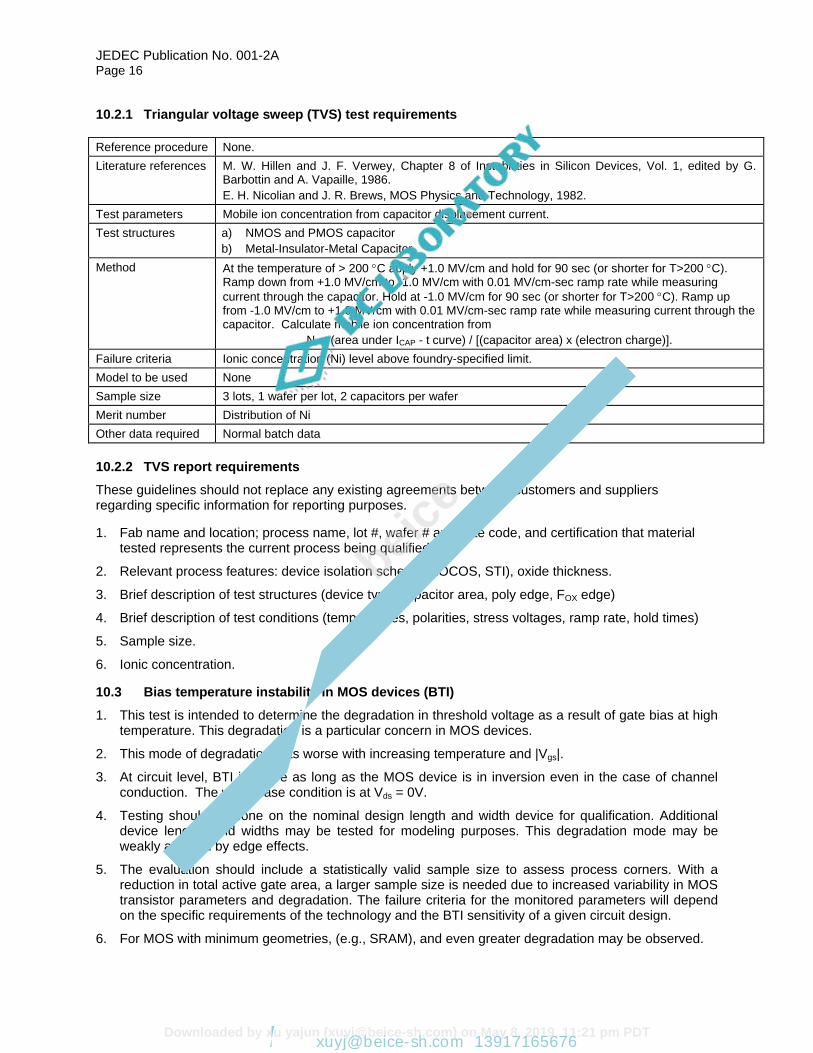
10.2.1 Triangular voltage sweep (TVS) test requirements
Reference procedure None.
Literature references M. W. Hillen and J. F. Verwey, Chapter 8 of Instabilities in Silicon Devices, Vol. 1, edited by G. Barbottin and A. Vapaille, 1986.
E. H. Nicolian and J. R. Brews, MOS Physics and Technology, 1982.
Test parameters Mobile ion concentration from capacitor displacement current.
Test structures a) NMOS and PMOS capacitor
b) Metal-Insulator-Metal Capacitor
Method At the temperature of > 200 C apply +1.0 MV/cm and hold for 90 sec (or shorter for T>200 C). Ramp down from +1.0 MV/cm to -1.0 MV/cm with 0.01 MV/cm-sec ramp rate while measuring
current through the capacitor. Hold at -1.0 MV/cm for 90 sec (or shorter for T>200 C). Ramp up from -1.0 MV/cm to +1.0 MV/cm with 0.01 MV/cm-sec ramp rate while measuring current through the capacitor. Calculate mobile ion concentration from
Ni = (area under ICAP - t curve) / [(capacitor area) x (electron charge)].
Failure criteria Ionic concentration (Ni) level above foundry-specified limit.
Model to be used None
Sample size 3 lots, 1 wafer per lot, 2 capacitors per wafer
Merit number Distribution of Ni
Other data required Normal batch data
10.2.2 TVS report requirements
These guidelines should not replace any existing agreements between customers and suppliers regarding specific information for reporting purposes.
1. Fab name and location; process name, lot #, wafer # and date code, and certification that material tested represents the current process being qualified.
2. Relevant process features: device isolation scheme (LOCOS, STI), oxide thickness.
3. Brief description of test structures (device type, capacitor area, poly edge, FOX edge)
4. Brief description of test conditions (temperatures, polarities, stress voltages, ramp rate, hold times)
5. Sample size.
6. Ionic concentration.
10.3 Bias temperature instability in MOS devices (BTI)
1. This test is intended to determine the degradation in threshold voltage as a result of gate bias at high temperature. This degradation is a particular concern in MOS devices.
2. This mode of degradation gets worse with increasing temperature and |Vgs|.
3. At circuit level, BTI is active as long as the MOS device is in inversion even in the case of channel conduction. The worst case condition is at Vds = 0V.
4. Testing should be done on the nominal design length and width device for qualification. Additional device lengths and widths may be tested for modeling purposes. This degradation mode may be weakly affected by edge effects.
5. The evaluation should include a statistically valid sample size to assess process corners. With a reduction in total active gate area, a larger sample size is needed due to increased variability in MOS transistor parameters and degradation. The failure criteria for the monitored parameters will depend on the specific requirements of the technology and the BTI sensitivity of a given circuit design.
6. For MOS with minimum geometries, (e.g., SRAM), and even greater degradation may be observed.
Downloaded by xu yajun ([email protected]) on May 8, 2019, 11:21 pm PDT
beice
北测
(上
海)
电子
科技
有限
公司
联系方式:[email protected] 13917165676

JEDEC Publication No. 001-2A Page 17
10.3.1 Bias temperature instability stress test requirements
Reference procedures
No PBTI standard exists yet.
Reference literature see JEP122 [5.3.1 – 5.3.18] TBD (GL)
Test parameters & failure criteria
VT to be measured from a single-point VT .( Note: In doing so, changes in other parameters that impact Vt may not be taken into account.) A DUT is considered to fail when the threshold voltage changes by more than the specified failure criterion after NBTI stress.
The failure criterion is a user-specified shift in VTLIN (or V VT Sat
Test structures MOSFET: nominal design length, for each allowed gate oxide thickness. See JESD28 & JESD60 for requirements.
DUT testable at last metal and passivation should be stressed
Vehicle Wafer Level or Packaged Level
Method DC Gate Bias Stress in “cold carrier” regime (Typically VDDMAX < VGS < (1.5) x |VDDmax.| with Vsb= 0V and Vdb=0V or in the linear mode (for fast switching methodology)
At BTI stress conditions avoid “hot carrier” injection from substrate typical of TDDB stressing conditions.
Test to be done at the maximum operating channel temperature (e.g., 125 C), held to an
accuracy of 2 C for the duration of stress test. A higher stress temperature may be used if the activation energy is measured.
Readouts (at stress temperature): Multiple Stress Cycle with readouts on a logarithmic time scale
[at least 2 points per decade recommended] (a time accuracy of 1%.) Interruption of the BTI stress for intermediate characterization must be kept to a minimum. The time between the end of BTI stress and the beginning of the characterization measurement must be controlled and the time must be recorded (to take recovery into account).
Typical model see JEP122, section 5.3 for reliability model
refer to JESD90 for potential values for the reliability models as they can vary depending on different technologies. Model expression and values listed below are for illustration only.
NBTI: VT =VT(t)-VT(0)=A x f(Wdes,Ldes) x |Vgs |α x exp(-H/kT) x t
P
PBTI: VT =VT(t)-VT(0)=A x f(Wdes,Ldes) x exp(*Vgs) x exp(-H/kT) x tP
where: VT(0) is the VT before stress, f(Wdes,Ldes) is an experimentally verified relation for the technology under investigation,
Time Dependence typically follows a power law: VT ~ tP, (p ≈ 0.16-0.25 as guideline.
Power law dependence (|Vgs |α ) with α around 3 – 4. Exponential field dependence with ~ 5-6.
Temperature dependence: Arrhenius with observed delta H around 0.05 to 0.2 eV.
Sample size 5 devices per wafer per bias condition x 3 lots.
Merit number VT Shift
Other data required Lot identification, Wafer Number, Gate oxide thickness, Channel length,BEOL and FEOL Processes, design channel lengths and widths used for NBTI stressing .
Downloaded by xu yajun ([email protected]) on May 8, 2019, 11:21 pm PDT
beice
北测
(上
海)
电子
科技
有限
公司
联系方式:[email protected] 13917165676

JEDEC Publication No. 001-2A Page 18
10.3.2 Report requirements
These guidelines should not replace any existing agreements between customers and suppliers regarding specific information for reporting purposes.
1. Fab name and location; process name, lot #, wafer # and date code, and certification that material tested represents the current process being qualified.
2. Relevant process features: device isolation scheme (LOCOS, STI), oxide thickness, minimum drawn device lengths, minimum LEFF.
3. Details on the VT Lin methodology
3.1 Details on measurement method and delay time.
4. Assumed VT Lin target
5. Brief description of test structures, test conditions and model used.
6. Sample size for each stress condition.
7. Extracted parameters for BTS degradation model(s), where applicable.
11 Technology qualification vehicle (TQV) tests
An appropriate technology qualification vehicle - SRAM or circuit of equivalent complexity is used to get a first look at the expected long-term failure rate of the process. Recommended SRAM sizes appear below and are based on SRAMs populated with a bit design and layout density expected to be typical at the respective lithographic node. For other qualification vehicles (e.g., ASIC), a number of circuits providing an equivalent density should be used.
Lithographic Node (nm)
SRAM size (Mb)
180 2
150 4
130 8
90 16
65 32
45/40 64
32/28 128
22/20 256
15 512
NOTE 1 An SRAM is an excellent vehicle where the primary concern is defect density. However, it has far too uniform a topology to be a good overall qualification vehicle in cases where divergent topologies may give rise to specific reliability concerns. Other vehicles may need to be used to provide a more thorough evaluation. NOTE 2 Evaluations driven by defect density require a larger number of samples where the vehicle size is reduced. For example, a 50% reduction in SRAM size would drive a 2x increase in the number of samples needed for a comparable measurement on a per circuit basis.
Downloaded by xu yajun ([email protected]) on May 8, 2019, 11:21 pm PDT
beice
北测
(上
海)
电子
科技
有限
公司
联系方式:[email protected] 13917165676

JEDEC Publication No. 001-2A Page 19
11.1 Long term life test The usefulness of a life test is dependent on an assessment of the dominant failure modes, as determined from a prior thorough analysis of failure modes (FMEA). See JEP131.
11.2 Detailed yield results
Reference procedure None
Test parameters Full Functional Test and IDDQ and Leakage Tests
Test structures Appropriate technology qualification vehicle
Vehicle Wafer Probe
Method NA
Model to be used Foundry Will specify Yield Model
Sample size 12 wafers from each of 6 lots
Defect density Defects per square centimeter
Other data required 1) Area of SRAM or other qualification vehicle
2) # of Critical Layers Used
3) Site location information relative to edge exclusion zone
11.3 Report requirements
These guidelines should not replace any existing agreements between customers and suppliers regarding specific information for reporting purposes.
1. Fab name and location; process name, lot #, wafer # and date code, and certification that material tested represents the current process being qualified.
2. Brief description of technology qualification vehicle: chip area, GOX area, circuit type (e.g., SRAM, ASIC), etc.
3. Test methodology & Test coverage, test speed (frequency), IDDQ limits.
4. Number of devices tested, devices passed and percent yield for each wafer tested. 5. Defect density per square cm.
Downloaded by xu yajun ([email protected]) on May 8, 2019, 11:21 pm PDT
beice
北测
(上
海)
电子
科技
有限
公司
联系方式:[email protected] 13917165676

JEDEC Publication No. 001-2A Page 20
12 Process control monitor (PCM) characterization
12.1 PCM data
The process control monitor (PCM) refers to the suite of test structures usually placed in the scribeline (alternatively named kerf, street or test key) separating product die on the wafer.
The parameter given in this section should be viewed as a suggested minimum set of E-test parameters. The foundry may choose a different set of parameters and/or tests to address specific yield, performance and reliability issues. The optimum set of parameters will depend on the specific customer product requirements.
This list is intended for correlation of qualification data to reliability models, circuit yield and performance improvement.
PCM parameters are to be provided for all agreed number of wafers and number of lots. As a minimum, these should include wafers used in qualification reliability testing (EM, SM, HCI, GOI, etc.)
Additional parameters may be included to meet specific customer needs or requirements.
It is highly recommended that the same parameters (or an agreed subset) be reported for subsequent prototype and production material, as part of a standard reporting schedule.
Test procedures are referenced where available. In all cases, the foundry should provide their specifications covering the test conditions and algorithms used, as well as the sampling plan.
Individual site data may be provided. Histograms, probability plots and trend charts are highly desirable. As a minimum, mean, standard deviation, minimums and maximums should be provided for each lot. Where possible, PCM data should quantify any dependence on site location relative to the wafer exclusion zone.
Reference procedures: JEDEC JEP132, and ASTM F616-86, 617-86 & 1096-87. 12.1.1 Requirements for logic circuits 1. MOSFET related parameters for both N and P channel MOSFETS
Long and wide MOSFET (NMOS and PMOS):
Linear threshold voltage: Single point method at a fixed current recommended. Alternate method(s) should be documented.
Optional: Gated diode breakdown with floating source.
Optional: Gamma Measured at [VBS] between 0 - (VDD/2)K' (beta) (KP) u COX BVDSF.
Shortest channel MOSFET (Minimum L NMOS and PMOS):
Linear threshold voltage (@ VDS = 0.1 V) and saturation threshold voltage (@VDS = VDDMAX). Single point method at a fixed current recommended. Alternate method(s) should be documented. Optional: Repeat at Vsub = -1.0 V for NFET and Vnw = +1.0 V for PFET.
Maximum substrate (or well) current ISUB: Measure at [VDS] = Max. VCC and [VGS] that gives maximum substrate current.
Drain current IDSAT: Measured at [VDS] = [VGS]=[VDDNOM], [VBS]=0. Optional: Repeat at [VDS] = [VGS] = [VDDMAX].
Drain OFF current IDOFF: Measured at [VDS] = VDDNOM], and VGS = VBS= 0. Optional: Repeat at [VDS] = [VDDMAX].
BVDSS transistor breakdown [VGS] = [VS] = [VBS] = 0, @1uA IDSS (ID0) (IOFF)
Delta L Channel length reduction (specify method)
Delta W Channel width reduction (specify method)
RS, RD Series resistances (from Long and Short transistors)
Downloaded by xu yajun ([email protected]) on May 8, 2019, 11:21 pm PDT
beice
北测
(上
海)
电子
科技
有限
公司
联系方式:[email protected] 13917165676

JEDEC Publication No. 001-2A Page 21
12.1.1 Requirements for logic circuits (cont’d) 2. Poly and metal 1 field VT with minimum isolation spacing (NMOS and PMOS)
Isolation Test (e.g., field threshold voltage VTF, or punch-through test). Specify Method. 3. Sheet resistances
Gate (poly): N+ and P+, where applicable
Well (N and/or P)
N+ diffusion
P+ diffusion
Metal (for all metal layers)
4. Contact resistance (Single contact and contact strings)
Gate (poly) Contact resistance
Well Contact resistance
N+ Contact resistance
P+ Contact resistance
Via (for all available via types)
N+ leakage measurements (from contact strings)
P+ leakage measurements (from contact strings) 5. Capacitances
Area capacitances: N+ and P+ diffusions
Overlap capacitances: NMOS & PMOS
6. Gate oxide integrity & gate oxide thickness
Gate oxide breakdown from V-RAMP test
Leakage at VDDMAX (NMOS/PMOS area/field/gate intensive capacitors, thin/thick oxides)
Gate oxide thickness (from C-V, F-N or charge pumping): To be determined for NMOS and PMOS capacitors in both accumulation and inversion. For thinner oxides (especially below ~ 5nm), QM effects and poly depletion should be taken into account. (See e.g., E. Wu et al, Proc. IRPS 1997, p. 184 and N. Yang et al, IEEE Trans. ED 46, no. 7, 1999, p. 1464).
Optional gate oxide parameters: flat-band voltage, interface states density (via C-V or charge pumping).
Metal integrity
Non-planar technologies: Isolation & Continuity Metal1/Metal2/Metal3 over topologies for filament (also known as short, ribbon, stringer).
Hot carriers
IGATE, ISUB and ID at VDDMAX (1.1*VDD) and VGS = VDDMAX [NMOS & PMOS LMIN FET]
IGATE, ISUB and ID at VDDMAX (1.1*VDD) VGS = VGS @ worst-case degradation condition [NMOS & PMOS LMIN FET]
Short HCI stress on NMOS and PMOS LMIN FETs under the following conditions:
NFET: Maximum substrate current
PFET: Maximum well current & VG=VD condition
Optional: Charge pumping interface state parameters.
Downloaded by xu yajun ([email protected]) on May 8, 2019, 11:21 pm PDT
beice
北测
(上
海)
电子
科技
有限
公司
联系方式:[email protected] 13917165676

JEDEC Publication No. 001-2A Page 22
12.1.1 Requirements for logic circuits (cont’d)
Ionic contamination
BTS: Delta VT & IOFF. NBTI
Short high temperature or field stress. P2ID
Short Fowler-Nordhein stress on NMOS/PMOS FETs connected to stacked antennas including all
metals and via levels to obtain ILG, VT before stress, VT and IDSAT of cumulative distributions.
12.1.2 For mixed signal/analog circuits add the following parameters
1. MOSFET related parameters long and wide MOSFET (e.g., 50/50) (NMOS and PMOS)
Gamma measured at [VBS] between 0-0.5, and VDDMAX/2 - VDDMAX. 2. Mid channel (2X or 5X of minimum drawn channel length) (NMOS and PMOS)
Output conductance [GDS]. Specify range.
Transconductance [GMMAX] or [Peak GM]
Asymmetry 180 degree rotated (or source and drain reversed) MOS transistor measurement (Ids % diff.)
3. Interlayer capacitors (POP, MIM, etc.)
TOX Interlayer dielectric thickness
Maximum voltage ratings
Leakage characteristics 4. Resistors (Implant or thin film resistors such as poly)
Contact resistance
Sheet resistances (If different than other measured sheet resistances)
Width reduction Calculated from resistance measurements on two resistors with different widths
Resistor values
Resistances for specific widths already measured for width calculations
Maximum current ratings
Self-heating and aging effects 5. BIPOLAR transistor parameters
For NPN, Lateral PNP, Substrate PNP, Isolated vertical PNP whenever applicable
Current gain [HFE] at defined IC, VCE. Two measurements: one at low IC and a second one at HFEMAX point.
Saturation current [IS]
Base-Emitter Voltage [VBE] at defined IC, VCE.
Early voltage [VEARLY] extracted from two defined VCE for defined IB
Collector-Emitter breakdown voltage [BVCEO] at defined IC
Collector-Base breakdown voltage [BVCBO] at defined IC
Collector-Emitter breakdown [BVCESC] with base-emitter shorted at defined IC.
It is desirable to obtain this data for two or more geometries of a particular transistor type (e.g., NPN1x, NPN10x, etc.).
Downloaded by xu yajun ([email protected]) on May 8, 2019, 11:21 pm PDT
beice
北测
(上
海)
电子
科技
有限
公司
联系方式:[email protected] 13917165676

JEDEC Publication No. 001-2A Page 23
12.1.1 Requirements for logic circuits (cont’d)
6. Dynamic Supply Effects
MOS and bipolar transistors used in RF and mixed signal blocks are often stressed with signal voltages that dynamically exceed VCC, e.g., with inductive loads (tank circuits, etc.).For such applications, it is appropriate to document the following characteristics:
Aging characteristics due to e.g., hot carrier and NBTI degradation Breakdown characteristics (gate oxide, emitter and collector junctions, etc.)
13 Construction analysis
13.1 Construction analysis Construction analysis is an essential tool to aid in evaluating process limitations and interpreting yield and reliability data. Construction analysis data provided by the foundry as part of the qualification package allows the customer to better understand the dependencies of their product on specific design rules. This may not substitute for detailed construction analysis done by the customer on the customer’s own product. Constructional analysis shall be performed on wafer or die to check the quality features. Any anomaly which has been encountered during the constructional analysis shall be documented and communicated to the appropriate engineering group for corrective action. Additional work shall be supplemented as required by the process technology. The constructional analysis results (visual or measurements) shall be documented in detail to demonstrate process attributes distribution. All visual documentation (Optical or SEM photos) shall display best case, typical, and worst case features. The parametric measurements shall record low, average, high and sigma values. 13.1.1 Construction analysis requirements
Reference procedure None
Test parameters A DUT is considered to fail if the design rule and physical measurement do not match in size shape or function.
Test structures a) Topographical SEM photos of minimum Metal, poly
b) Cross sectional SEM photos of all critical levels including each metal level, via, contact, poly, oxides and silicon isolation scheme.
Vehicle Fully processed baseline wafers.
Method a) Optical photographs for wide angle views and orientation location
b) SEM of each individual layer and
c) TEM of gate oxide and flash oxides.
Model to be used
Sample size Three lots with a minimum one die.
Merit number The variation in film thickness and/or line-width should be consistent with design manual assumptions.
Other data required Line width, thickness, composition of metal lines, via dimensions and alignment to metal lines.
Downloaded by xu yajun ([email protected]) on May 8, 2019, 11:21 pm PDT
beice
北测
(上
海)
电子
科技
有限
公司
联系方式:[email protected] 13917165676

JEDEC Publication No. 001-2A Page 24
13.1.2 Reporting requirements
1. Fab name and location; process name, lot #, wafer # and date code, and certification that material tested represents the current process being qualified.
2. Back end scheme: thickness, composition for each layer, via type (Tungsten, etc.), inter-level dielectric.
3. Relevant design rules: minimum widths, minimum spaces, contact and via sizes.
Downloaded by xu yajun ([email protected]) on May 8, 2019, 11:21 pm PDT
beice
北测
(上
海)
电子
科技
有限
公司
联系方式:[email protected] 13917165676

JEDEC Publication No. 001-2A Page 25
Annex A (informative) Differences between revisions
A.1 Differences between JEP001-2A to JEP001A The following list briefly describes most of the changes made to entries that appear in this publication, JEP001-2A , compared to its predecessor, JEP001A (February 2014).
Clause Description of Change
All JEP001A Split into three parts: JEP001-1A Backend of Line, JEP001-2A,
FEOL End Transistor Level and JEP001-3A Product level.
Downloaded by xu yajun ([email protected]) on May 8, 2019, 11:21 pm PDT
beice
北测
(上
海)
电子
科技
有限
公司
联系方式:[email protected] 13917165676

JEDEC Publication No. 001-2A Page 26
Downloaded by xu yajun ([email protected]) on May 8, 2019, 11:21 pm PDT
beice
北测
(上
海)
电子
科技
有限
公司
联系方式:[email protected] 13917165676

Standard Improvement Form JEDEC
The purpose of this form is to provide the Technical Committees of JEDEC with input from the industry regarding usage of the subject standard. Individuals or companies are invited to submit comments to JEDEC. All comments will be collected and dispersed to the appropriate committee(s). If you can provide input, please complete this form and return to:
JEDEC Attn: Publications Department 3103 North 10
th Street
Suite 240 South Arlington, VA 22201-2107
Fax: 703.907.7583
1. I recommend changes to the following:
Requirement, clause number
Test method number Clause number
The referenced clause number has proven to be:
Unclear Too Rigid In Error
Other
2. Recommendations for correction:
3. Other suggestions for document improvement:
Submitted by
Name: Phone:
Company: E-mail:
Address:
City/State/Zip: Date:
Downloaded by xu yajun ([email protected]) on May 8, 2019, 11:21 pm PDT
beice
北测
(上
海)
电子
科技
有限
公司
联系方式:[email protected] 13917165676

Downloaded by xu yajun ([email protected]) on May 8, 2019, 11:21 pm PDT
beice
北测
(上
海)
电子
科技
有限
公司
联系方式:[email protected] 13917165676