Embed Size (px)
Citation preview
FPGA and Digital SignalProcessing Laboratory Guide
1 Introduction
The laboratory consists of 9 labs. The goal of these labs is to give thestudents experience in developing simple DSP applications realized in FPGAdevices. The labs make use of Memec’s Spartan-3 development kit togetherwith analog module containing fast analog-to-digital (ADC) and digital-to-analog (DAC) converters. The development kit is based on Xilinx XC3S400chip derived from Spartan-3 FPGA family.
Xilinx Integrated Software Environment (ISE) is used by students to de-velop projects. The main design entries are VHDL project description filesand Xilinx predefined building blocks named Intellectual Property (IP) cores.The software supports automatic synthesis, placement and routing of a de-sign. A bit-file obtained as a result of these operations may be used toconfigure the Spartan FPGA device included in the development board. TheJTAG programming cable attached to the PC parallel port makes it possibleto download a bit-file directly into the FPGA device.
In the next sections a brief description of the Spartan-3 FPGA devices,the Memec development kit and the ISE software environment is given. Thenthe individual lab exercises are described. In the last section the main VHDLkeywords and statements are briefly described.
2 Spartan-3 FPGA family overview
The Spartan-3 family architecture consists of five fundamental programmablefunctional elements:
• Configurable Logic Blocks (CLBs) containing RAM-based Look-Up Ta-bles (LUTs) to implement logic and storage elements that can be usedas flip-flops or latches. CLBs can be programmed to perform a widevariety of logical functions as well as to store data.
• Input/Output Blocks (IOBs) controlling the flow of data between theI/O pins and the internal logic of the device.
• 18-Kbit dual-port RAM blocks providing data storage.
1
• Multiplier blocks which accept two 18-bit binary numbers as inputsand calculate the product.
• Digital Clock Manager (DCM) blocks provide self-calibrating, fullydigital solutions for distributing, delaying, multiplying, dividing, andphase shifting clock signals.
These elements are organized as shown in Figure 1. A ring of IOBssurrounds a regular array of CLBs. The XC3S400 device contains 896 CLBs,288kbit embedded RAM, 16 dedicated multipliers and 4 DCMs.
Figure 1: Spartan-3 family architecture
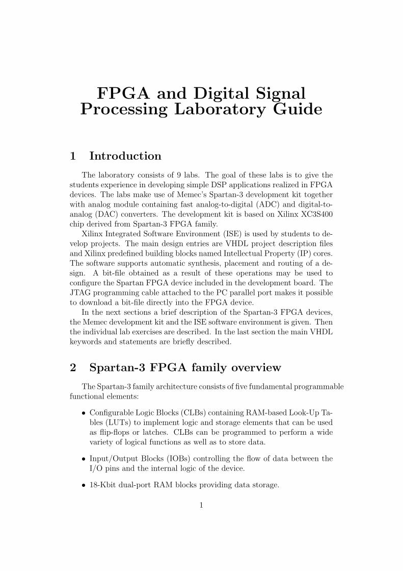
The main logic resource for implementing synchronous as well as combi-natorial circuits is the Configurable Logic Block (CLB). Each CLB comprisesfour interconnected slices, as shown in Figure 2. These slices are grouped inpairs. Each pair is organized as a column with an independent fast carrychain. The carry chain supports implementing arithmetic functions such asaddition.
All four slices have the following elements in common: two logic func-tion generators (known as Look-Up Tables), two flip-flops, wide-functionmultiplexers, carry logic, and auxiliary arithmetic gates. The RAM-basedLook-Up Table (LUT) is the main resource for implementing logic functions.Each of the two LUTs in a slice have four logic inputs and a single output.This permits any four-variable Boolean logic operation to be programmedinto them. Wide-function multiplexers can be used to effectively combine
2
Figure 2: Configurable Logic Block
LUTs within the same CLB or across different CLBs, making logic functionswith many more input variables possible.
Switch matrix (see Figure 2) allows programmable access into local andglobal routing resources. Clock signals are distributed by dedicated low-capacitance, low-skew network well suited to carrying high-frequency signals.
Spartan-3 FPGAs are programmed by loading configuration data intostatic memory cells that control all functional elements and routing resources.Before powering on the FPGA, configuration data is stored externally in aPROM or some other nonvolatile medium either on or off the board. Afterapplying power, the configuration data is written to the FPGA using one ofthe available modes, e.g. JTAG mode.
More detaile information about Spartan-3 FPGA devices is available inData Sheet [3].
3
3 Memec Spartan-3 LC Development Board
and P160 Analog Module
3.1 Memec Spartan-3 LC Development Board
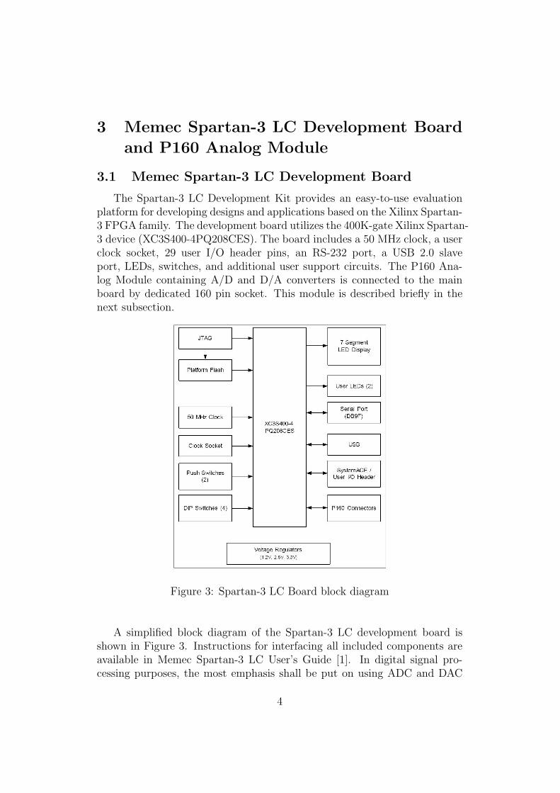
The Spartan-3 LC Development Kit provides an easy-to-use evaluationplatform for developing designs and applications based on the Xilinx Spartan-3 FPGA family. The development board utilizes the 400K-gate Xilinx Spartan-3 device (XC3S400-4PQ208CES). The board includes a 50 MHz clock, a userclock socket, 29 user I/O header pins, an RS-232 port, a USB 2.0 slaveport, LEDs, switches, and additional user support circuits. The P160 Ana-log Module containing A/D and D/A converters is connected to the mainboard by dedicated 160 pin socket. This module is described briefly in thenext subsection.
Figure 3: Spartan-3 LC Board block diagram
A simplified block diagram of the Spartan-3 LC development board isshown in Figure 3. Instructions for interfacing all included components areavailable in Memec Spartan-3 LC User’s Guide [1]. In digital signal pro-cessing purposes, the most emphasis shall be put on using ADC and DAC
4
components.
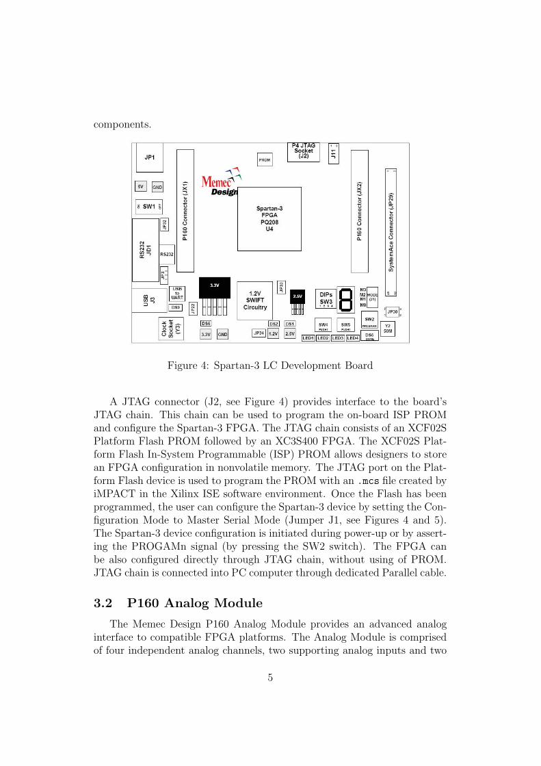
Figure 4: Spartan-3 LC Development Board
A JTAG connector (J2, see Figure 4) provides interface to the board’sJTAG chain. This chain can be used to program the on-board ISP PROMand configure the Spartan-3 FPGA. The JTAG chain consists of an XCF02SPlatform Flash PROM followed by an XC3S400 FPGA. The XCF02S Plat-form Flash In-System Programmable (ISP) PROM allows designers to storean FPGA configuration in nonvolatile memory. The JTAG port on the Plat-form Flash device is used to program the PROM with an .mcs file created byiMPACT in the Xilinx ISE software environment. Once the Flash has beenprogrammed, the user can configure the Spartan-3 device by setting the Con-figuration Mode to Master Serial Mode (Jumper J1, see Figures 4 and 5).The Spartan-3 device configuration is initiated during power-up or by assert-ing the PROGAMn signal (by pressing the SW2 switch). The FPGA canbe also configured directly through JTAG chain, without using of PROM.JTAG chain is connected into PC computer through dedicated Parallel cable.
3.2 P160 Analog Module
The Memec Design P160 Analog Module provides an advanced analoginterface to compatible FPGA platforms. The Analog Module is comprisedof four independent analog channels, two supporting analog inputs and two
5
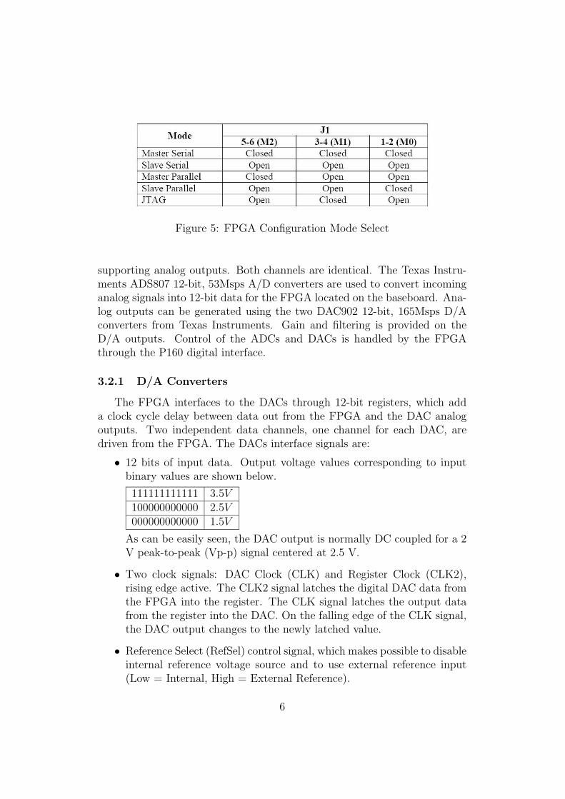
Figure 5: FPGA Configuration Mode Select
supporting analog outputs. Both channels are identical. The Texas Instru-ments ADS807 12-bit, 53Msps A/D converters are used to convert incominganalog signals into 12-bit data for the FPGA located on the baseboard. Ana-log outputs can be generated using the two DAC902 12-bit, 165Msps D/Aconverters from Texas Instruments. Gain and filtering is provided on theD/A outputs. Control of the ADCs and DACs is handled by the FPGAthrough the P160 digital interface.
3.2.1 D/A Converters
The FPGA interfaces to the DACs through 12-bit registers, which adda clock cycle delay between data out from the FPGA and the DAC analogoutputs. Two independent data channels, one channel for each DAC, aredriven from the FPGA. The DACs interface signals are:
• 12 bits of input data. Output voltage values corresponding to inputbinary values are shown below.
111111111111 3.5V100000000000 2.5V000000000000 1.5V
As can be easily seen, the DAC output is normally DC coupled for a 2V peak-to-peak (Vp-p) signal centered at 2.5 V.
• Two clock signals: DAC Clock (CLK) and Register Clock (CLK2),rising edge active. The CLK2 signal latches the digital DAC data fromthe FPGA into the register. The CLK signal latches the output datafrom the register into the DAC. On the falling edge of the CLK signal,the DAC output changes to the newly latched value.
• Reference Select (RefSel) control signal, which makes possible to disableinternal reference voltage source and to use external reference input(Low = Internal, High = External Reference).
6

• Power Down (PD) control signal (Low = Normal, High = Power DownMode).
3.2.2 A/D converters
Texas Instruments ADS807 converters provide 12-bit resolution at up to53 Msps. The digital data out of the A/Ds is latched into external buffersand then passed to the FPGA through the P160 interface. The range ofthe input voltage is dependent on the Full Scale Select control signal to theA/D. Before conversion the input signal is AC coupled, biased to 2.5 voltsfor unipolar operation, and buffered through the op amp.The ADCs interfacesignals are:
• 12 bits of output data (binary range ”000000000000” to ”111111111111”).
• Full Scale Select control signal (FsSel). Setting this signal to a logichigh allows a 1.5 Vp-p input to the board. Setting the Full ScaleSelect to low, selects a 1 Vp-p input range to the board (i.e. −0.5Vvoltage corresponds to ”000000000000” value and +0.5V correspondsto ”111111111111” value).
• Reference Select (RefSel) control signal (Low = Internal Reference,High = External Reference).
• Output Enable (OE) control signal (Low = Output Enabled, High =Tri-Stated outputs).
• Convert clock (CLK) signal. The ADS807 samples the input signal onthe rising edge of the CLK input. Output data values are valid at theoutputs 6 clock cycles later, after the rising edge of the clock.
More detailed information about the Analog Module is available in [2].
4 Xilinx Integrated Software Environment (ISE)
The Xilinx Integrated Software Environment (ISE) is a complex set oftools to design programmable logic devices projects. ISE tools allow thedesign to be entered several ways including graphical schematics, state ma-chine diagrams, VHDL, Verilog and Intelectual Property (IP) cores. Thisguide will focus on VHDL entry, but the other methods are similar and canbe easily explored once the reader is comfortable with the ISE software.
The primary ISE tools used in this laboratory are:
7
• ISE Project Navigator which integrates all ISE tools and provides win-dows displaying project hierarchy and the design process, as well as acontext-sensitive HDL Editor.
• Core Generator module which offers an optimized, predefined set ofbuilding blocks for common functions - simplifying design steps andbringing the design to completion faster.
• iMPACT tool that allows to configure FPGA devices through JTAGprogramming cable.
• ModelTechnology ModelSim that enables functional simulation of aVHDL design.
4.1 HDL design flow
The process of converting hardware description language (HDL) files intoa configuration bitstream which can be used to program the FPGA, is donein several steps.
First, the HDL files are synthesized. Synthesis is the process of convert-ing behavioral HDL descriptions into a network of logic gates. The synthesisengine takes as input the HDL design files and a library of primitives. Prim-itives are not necessarily just simple logic gates like AND and OR gates andD-registers, but can also include more complicated things such as shift regis-ters and arithmetic units. Primitives also include specialized circuits such asDCMs (Digital Clock Manager) that cannot be inferred by behavioral HDLcode and must be explicitly instantiated. The libraries guide in the Xilinxdocumentation provides an complete description of every primitive availablein the Xilinx library. There are occasions when it is helpful or even necessaryto explicitly instantiate primitives, but it is much better design practice towrite behavioral code whenever possible.
Synthesis process is supported by Xilinx engine known as XST. XST takesas input a verilog or VHDL file and generates a .ngc file. A synthesis reportfile (.srp) is also generated, which describes the logic inferred for each partof the HDL file, and often includes helpful warning messages.
The .ngc file is then converted to an .ngd file. This step mostly seems tobe necessary to accommodate different design entry methods, such as third-part synthesis tools or direct schematic entry. Whatever the design entrymethod, the result is an .ngd file.
The .ngd file is essentially a netlist of primitive gates, which could beimplemented on any one of a number of types of FPGA devices Xilinx man-ufacturers. The next step is to map the primitives onto the types of resources
8
(logic cells, i/o cells, etc.) available in the specific FPGA being targeted. Theoutput of the Xilinx map tool is an .ncd file.
The design is then placed and routed, meaning that the resources de-scribed in the .ncd file are then assigned specific locations on the FPGA, andthe connections between the resources are mapped into the FPGAs inter-connect network. The delays associated with interconnect on a large FPGAcan be quite significant, so the place and route process has a large impacton the speed of the design. The place and route engine attempts to honortiming constraints that have been added to the design, but if the constraintsare too tight, the engine will give up and generate an implementation thatis functional, but not capable of operating as fast as desired.
The output of the place and route engine is an updated .ncd file, whichcontains all the information necessary to implement the design on the chosenFPGA. All that remains is to translate the .ncd file into a configurationbitstream in the format recognized by the FPGA programming tools. Thenthe programmer is used to download the design into the FPGA, or writethe appropriate files to a flash PROM, which is then used to configure theFPGA.
4.2 Constraints
Project implementation information such as device pin allocations and pinelectrical properties are usually not stored in HDL source files, they are storedin separate constraints files. Constraints specify placement, implementation,naming, signal direction, and timing considerations for timing analysis andfor design implementation. Constraints can be defined by manually editingascii file (with extension .ucf - User Constraint File) or defined using Pinoutand Area Constraints Editor (PACE) application as well as Constraint Editorapplication.
A .ucf file is simply a list of constraints, such asNET "Dip<3>" LOC = "P26";
which indicates that bit 3 of the signal Dip (which should be a port in the top-level HDL module) should be assigned to pin P26 on the FPGA. Sometimesit is useful to combine several related constraints on one line, using ”|”characters to separate constraints.NET "Dip<3>" loc="P26" | FAST | IOSTANDARD=LVDCI 33 | DRIVE=12;
The above example again assigns bit 3 of the signal Dip to pin P26, andalso specifies that the i/o driver should be configured for fast slew rate, 3.3VLVTTL level signaling (with a built-in series termination resistor), and adrive strength of 12mA. All of the necessary pin constraints for the MemecDevelopment Board have been written for you in a template UCF file.
9
4.3 Core Generator
The Xilinx CORE Generator System provides a catalog of user-customizableblocks ranging in complexity from simple arithmetic operators (adders, ac-cumulators, and multipliers), memories and FIFOs, to networking interfacesand DSP building blocks such as filters and transforms.
You can start the CORE Generator from the ISE environment or directlyfrom Windows environment. Before starting the CORE Generator, an ISEproject should be created, so generated cores will be added to it.
For each core it generates, the CORE Generator System produces anElectronic Data Interchange Format (.edn) netlist file (EDN file), a VHDL(or Verilog) template file (.vho) and a VHDL (Verilog) wrapper file (.vhd).It may also create one or more NGC and NDF files. NGC files are producedfor certain cores only.
The Electronic Data Netlist (EDN) and NGC files contain the informationrequired to implement the module in a Xilinx FPGA. VHD wrapper file isprovided to support functional simulation. VHO template file contains codethat can be used as a template for instantiating a core in a VHDL design. Theonly thing to do is to copy and paste component declaration and instantiationfrom this VHO file into your design (renaming the signals if needed) and addEDN netlist into project.
4.4 iMPACT
Xilinx iMPACT, which can be started from ISE or directly from oper-ating system, enables you to configure PLD designs through four modes ofconfiguration, among which is JTAG mode that is used for the DevelopmentBoard. Using JTAG programming cable you can configure FPGA and/orstore configuration in the flash PROM.
Before downloading configuration into XCF02S Platform Flash PROM,an appropriate PROM configuration bit-file have to be created. Such file(with extension .mcs) can be created in iMPACT application (File Genera-tion Mode).
10
5 Laboratory exercises
5.1 Lab 1: Introduction to ISE software and MemecSpartan-3 Development Kit. Interfacing A/D andD/A converters.
The purpose of the first Lab is to give the students opportunity to famil-iarize with the tools used in the laboratory.
A simple ISE project template suitable for use with the DevelopmentKit is available for you. The template consists of project file Template.npl,VHDL source file Templatetop.vhd and user constraints file Memec kit.ucf.The VHDL source file contains a top level entity declaration and its archi-tecture body definition. The entity declaration is as follows:
entity Templatetop is
Port (
Clk_in : in std_logic; --50MHz clock input
Dac1 : out std_logic_vector(11 downto 0); --DAC 1 data
Dac1_PD, Dac1_Clk, Dac1_Clk2, Dac1_RefSel : out std_logic;
--DAC 1 control signals
Dac2 : out std_logic_vector(11 downto 0); --DAC 2 data
Dac2_PD, Dac2_Clk, Dac2_Clk2, Dac2_RefSel : out std_logic;
--DAC 2 control signals
Adc1 : in std_logic_vector(11 downto 0); --ADC 1 data
Adc1_fssel, Adc1_refsel, Adc1_oe, Adc1_clk : out std_logic;
--ADC 1 control signals
Adc2 : in std_logic_vector(11 downto 0); --ADC 2 data
Adc2_fssel, Adc2_refsel, Adc2_oe, Adc2_clk : out std_logic;
--ADC 2 control signals
Push1, Push2 : in std_logic; --Pushbuttons
Dip : in std_logic_vector(3 downto 0); --DIP switch
Led : out std_logic_vector(4 downto 1); --LEDs
Display : out std_logic_vector(6 downto 0); --LED Display
USB_RESET, USB_DSR, USB_CTS,
USB_DCD, USB_RI, USB_Tx : out std_logic;
USB_DTR, USB_RTS, USB_Rx : in std_logic
--USB port data and control signals
);
end Templatetop;
Unused port declarations shall be removed when designing particular projects,as well as the UCF file should be edited to remove constraints for unused pins.
11
Remember that port names in the top level entity and in the UCF file haveto be identical.
The architecture body contains description of the clock distribution net-work making use of the DCM (Digital Clock Manager) and simple port signalsassignments to set appropriate DAC and ADC control signals as well as toturn the LED and Display lights off.
The clock distribution network consists of DCM and buffers for incomingclock signal and for output clock to DAC and ADC (BUFG and OBUF compo-nents). The primary task for the DCM is to provide suitably phase shiftedclock for DAC clocking. The DAC data output from FPGA is changing syn-chronously to main FPGA clock signal, thus the DAC clock signal have tobe phase shifted to avoid signal glitches in the DAC analog output. The 90◦
shifted clock signal (from Clk90 output of the DCM) is provided to the DAC.
Preparations
• Read carefully previous sections of this Laboratory Guide.
Assignments
• Start ISE Project Navigator. Create a new project with HDL top-level module type. Select Spartan3 device family, XC3S400 device,pq208 package. Add a new VHDL source file with entity containingone input port Push1 and one output Led1. Create a new text file, saveit with .ucf extension and add it to the project. Write the followingconstraints in the UCF file:
NET "Push1" LOC = "P22" | PULLUP | IOSTANDARD = LVCMOS33;
NET "Led1" LOC = "P19" | FAST | DRIVE = 24 |
IOSTANDARD = LVCMOS33;
In the architecture body, write a single line that allows to switch onand off the LED1 by pushing the Pushbutton on the Board (Led1 <=
Push1;). Compile the project by double clicking on Generate Program-ming File in Processes for Source window.
After successful programming file generation, download the Bitstreamto the FPGA on the board. Make sure that JTAG cable is properlyconnected to the Board and start iMPACT application. Select op-tions: Boundary-Scan Mode, then Automatically identify Boundary-Scan chain. A window with JTAG chain similar to that shown in
12
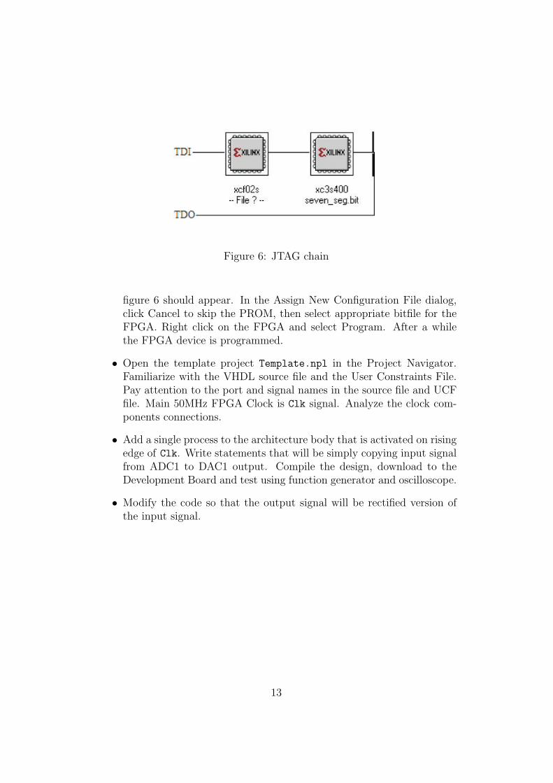
Figure 6: JTAG chain
figure 6 should appear. In the Assign New Configuration File dialog,click Cancel to skip the PROM, then select appropriate bitfile for theFPGA. Right click on the FPGA and select Program. After a whilethe FPGA device is programmed.
• Open the template project Template.npl in the Project Navigator.Familiarize with the VHDL source file and the User Constraints File.Pay attention to the port and signal names in the source file and UCFfile. Main 50MHz FPGA Clock is Clk signal. Analyze the clock com-ponents connections.
• Add a single process to the architecture body that is activated on risingedge of Clk. Write statements that will be simply copying input signalfrom ADC1 to DAC1 output. Compile the design, download to theDevelopment Board and test using function generator and oscilloscope.
• Modify the code so that the output signal will be rectified version ofthe input signal.
13
5.2 Lab 2: Simple signal generation (square, triangle,sawtooth).
The purpose of this lab is to design simple linear signals generator.
Assignments
• Create a new project for Spartan XC3S400 device. Copy source codefrom Templatetop.vhd and add to project a copy of UCF file Memec kit.ucf.Remove all ports except of DAC1 data and control signals ports.
• Modify the project to generate square wave on the DAC1 output. Re-quired frequency of the signal will be given to students during lab.
• Modify the project to allow changing frequency by switching pushbut-tons, i.e. switching one pushbutton should increase frequency and theother – decrease.
• Add ports to interface second DAC (DAC2) to the top entity. Generatethe sawtooth wave on the second DAC output. To achieve this, a simplecounter should be created and its output connected to the DAC2 datainput. Allow changing frequency of the sawtooth wave.
• Design the triangle wave generator and similarly allow changing fre-quency.
14

5.3 Lab 3: Sine wave generation by Look-Up Tableand CORDIC algorithm.
In this lab the students are required to design a sine wave generator. Twomethods to accomplish this task will be tested. The first is using Sine/CosineLook-Up Table core and the second – using CORDIC algorithm core. TheXilinx Core Generator supports making use of these cores.
Preparations
• Read the Sine/Cosine Look-Up Table core specification.
• Read the CORDIC core specification.
Assignments
• After creating a new ISE project, start Core Generator system. Fromthe list of available cores, find the Sine/Cosine Look-Up Table. Spec-ification of each core is available after right clicking the core name inthe list. Open datasheet with Sine/Cosine Look-Up Table specificationand read through it.
• Generate the Sine/Cosine Look-Up Table core. Add it to the ISEproject and copy from .vho file the component declaration and instan-tiation templates into your design.
• To generate sine wave, the Look-Up Table input should be fed by con-stantly growing argument (from 0 to 2π and so forth). The core com-putes sin(θ) where
θ = THETA2π
2THETA WIDTH[rad]
where THETA is an integer input angle. Outputs sine and cosine areexpressed as fractional fixed-point values. See specification of the corefor more details. Generate sine wave of given frequency and observe iton the oscilloscope. Note that the DAC input value is in an unsignedformat, thus simple conversion of Look-Up Table output have to bedone.
• Create a new project. Generate CORDIC core in the Core Generator.The CORDIC core implements a generalized coordinate rotational dig-ital computer (CORDIC) algorithm, to iteratively solve trigonometric,hyperbolic and square root equations. More details about this algo-rithm is available in the CORDIC core specification. Generate sinewave using this core.
15

• Compare resources occupied by generators designed by both methods.The number of used CLBs, LUTs, memory blocks and multiplier blockscan be read from Map Report file as well as Place & Route Report file.
16
5.4 Lab 4: Amplitude modulation: AM, DSB-SC.
The purpose of this lab is to design simple amplitude modulators: AMand DSB-SC (Double SideBand Suppressed Carrier).
Preparations
• Read the Multiplier core specification.
Assignments
• Design DSB-SC modulator. The modulating signal from ADC1 inputshould modulate amplitude of the carrier signal. The carrier sinusoidalsignal is generated inside the FPGA. Thus the design should consist ofsine generator (similar to that created in the previous lab exercise) andmultiplier that calculates the product of the carrier and modulatingsignal from ADC. The carrier frequency will be given during the lab.The multiplier can be designed using Multiplier core or directly instan-tiated – Xilinx library includes MULT18X18 and MULT18X18S elementsthat represents embedded multiplier blocks in the FPGA (see Spartan-3 supported design elements [4]). However, using of the Multiplier coreis more flexible. Create DSB-SC modulator using both methods offorming multiplier.
• Design AM modulator. Since the AM signal is DSB plus carrier, it canbe generated by simply adding synchronous carrier to the DSB signal.
• Observe the AM signal on the oscilloscope when the modulating signalis sine with 1V peak-to-peak. Calculate the modulation index of thesignal. Change the project to obtain modulation index 0.5.
17
5.5 Lab 5: FIR filter design using Distributed Arith-metic FIR core.
In this lab a Finite Impulse Response filter will be realized by students.The Distributed Arithmetic FIR Filter core will be used.
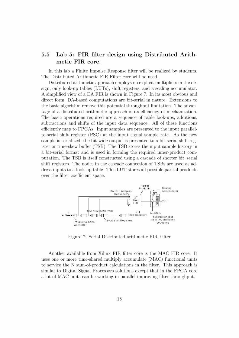
Distributed arithmetic approach employs no explicit multipliers in the de-sign, only look-up tables (LUTs), shift registers, and a scaling accumulator.A simplified view of a DA FIR is shown in Figure 7. In its most obvious anddirect form, DA-based computations are bit-serial in nature. Extensions tothe basic algorithm remove this potential throughput limitation. The advan-tage of a distributed arithmetic approach is its efficiency of mechanization.The basic operations required are a sequence of table look-ups, additions,subtractions and shifts of the input data sequence. All of these functionsefficiently map to FPGAs. Input samples are presented to the input parallel-to-serial shift register (PSC) at the input signal sample rate. As the newsample is serialized, the bit-wide output is presented to a bit-serial shift reg-ister or time-skew buffer (TSB). The TSB stores the input sample history ina bit-serial format and is used in forming the required inner-product com-putation. The TSB is itself constructed using a cascade of shorter bit–serialshift registers. The nodes in the cascade connection of TSBs are used as ad-dress inputs to a look-up table. This LUT stores all possible partial productsover the filter coefficient space.
Figure 7: Serial Distributed arithmetic FIR Filter
Another available from Xilinx FIR filter core is the MAC FIR core. Ituses one or more time-shared multiply accumulate (MAC) functional unitsto service the N sum-of-product calculations in the filter. This approach issimilar to Digital Signal Processors solutions except that in the FPGA corea lot of MAC units can be working in parallel improving filter throughput.
18
Preparations
• Read the Distributed Arithmetic Fir Filter core documentation.
• Calculate the filter coefficients from given in advance filter specification.This calculation could be done for example using Matlab Filter Design& Analysis Tool.
• Write the calculated coefficients in the Xilinx .coe file format. Thisis an ASCII text file with a single-line header that defines the radix(base-2, base-10, or base-16) of the number representation used forthe coefficient data, followed by the coefficient values themselves. Anexample is shown below for an 8-tap filter.
radix=10;
coefdata=20, -256, 200, 255,39, 117, -235, 47;
The coefficient values may also be placed on separate lines.
When using Matlab FDA Tool, the .coe file can be generated auto-matically.
Assignments
• Create a new project, making use of the Template project. Generateand instantiate the Distributed Arithmetic FIR Filter core using previ-ously written .coe coefficient file and selecting parallel implementationoption.
• Compile the design and download to the Development Board. Checkhow it works using function generator and oscilloscope.
• To allow frequency response measurement by spectrum analyzer, changefilter clock frequency to 100kHz. This requires designing appropriateclock frequency divider.
• Measure the frequency response of filter using HP35665 spectrum ana-lyzer. Save data into floppy disc and open the file in the PC computer.The data can be read by Viewdata.exe application as well as convertinto ascii format by Sdftoasc.exe application. More details will begiven during lab.
19

• Regenerate the DA FIR Filter core selecting serial implementation.Compare the resources (CLBs, LUTs, RAM and multiplier blocks) oc-cupied by both filter realizations. What is the maximum samplingfrequency in these cases?
Report
• Create report including magnitude and phase response of the designedfilter measured by spectrum analyzer.
20
5.6 Lab 6: Demodulation of AM signal.
The purpose of this lab is to design AM demodulator. The simplest wayto realize AM demodulation is an envelope detector that tracks the peaks ofthe signal waveform. Envelope detection can be realized as rectification andthen low pass filtration of AM signal.
Preparations
• Calculate coefficients of an appropriate low pass FIR filter for envelopedetection. The filter shall be used for the AM signal detection (sam-pling frequency 50MHz) with maximum frequency of modulating signal20kHz and carrier frequency 2MHz. The filter should have maximum3dB ripple in the modulating signal band (0 – 20kHz) and minimum40dB attenuation of carrier frequency signal.
Assignments
• Design envelope detector consisting of rectifier and low pass FIR filtermeeting specifications given above. Use Distributed Arithmetic FIRFilter core with full parallel realization. Carrier frequency should equal2MHz.
• In this lab, two Development Boards shall be used. Download intothe first Board configuration of AM modulator created during the 4thlab. Then, download into the second board configuration of AM de-modulator. Connect input of the modulator to the function generatorand observe simultaneously signals on the input and the output of thedemodulator. Try different types and frequencies of modulating signal.
21
5.7 Lab 7: Fast Fourier Transform (FFT)
The goal of this lab is to implement the Fast Fourier Transform calcu-lation. To achieve it Xilinx FFT core is used. The FFT core computes anN-point forward DFT or inverse DFT (IDFT) where N can be 2m, m = 3–16.
Preparations
• Read the Fast Fourier Transform core documentation
• Read the Using Block RAM in Spartan-3 FPGAs application note fromXilinx
Assignments
• Create a new project. Generate a 256-point FFT core.
• Design project for calculating a 256-point FFT of input from ADC1signal and storing results in a Block RAM. FFT shall be calculatedafter pushing PUSH1 button. Dual port block RAM should be used:one port for writing FFT and another for reading data.
• FFT results shall be displayed on the oscilloscope. Thus in one of theDAC outputs a periodically repeated signal representing the calculatedFFT should be generated. In the other analog output, a pulses forsynchronizing the oscilloscope should be generated.
• Observe spectrum of the basic signals: sine, rectangular, triangle andAM.
• Change width of the FFT to 1024 points.
22
5.8 Lab 8: IIR filter design.
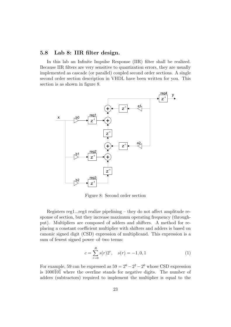
In this lab an Infinite Impulse Response (IIR) filter shall be realized.Because IIR filters are very sensitive to quantization errors, they are usuallyimplemented as cascade (or parallel) coupled second order sections. A singlesecond order section description in VHDL have been written for you. Thissection is as shown in figure 8.
+z-1
b0reg1
z-1
+z-1
b1reg2
+
z-1
z-1
b2reg3
z-1
a2
z-1 a1
+
x
yz
-1
reg4
Figure 8: Second order section
Registers reg1...reg4 realize pipelining – they do not affect amplitude re-sponse of section, but they increase maximum operating frequency (through-put). Multipliers are composed of adders and shifters. A method for re-placing a constant coefficient multiplier with shifters and adders is based oncanonic signed digit (CSD) expression of multiplicand. This expression is asum of fewest signed power–of–two terms:
c =R∑
r=0
s(r)2r, s(r) = −1, 0, 1 (1)
For example, 59 can be expressed as 59 = 26−22
−20 whose CSD expressionis 1000101 where the overline stands for negative digits. The number ofadders (subtractors) required to implement the multiplier is equal to the
23
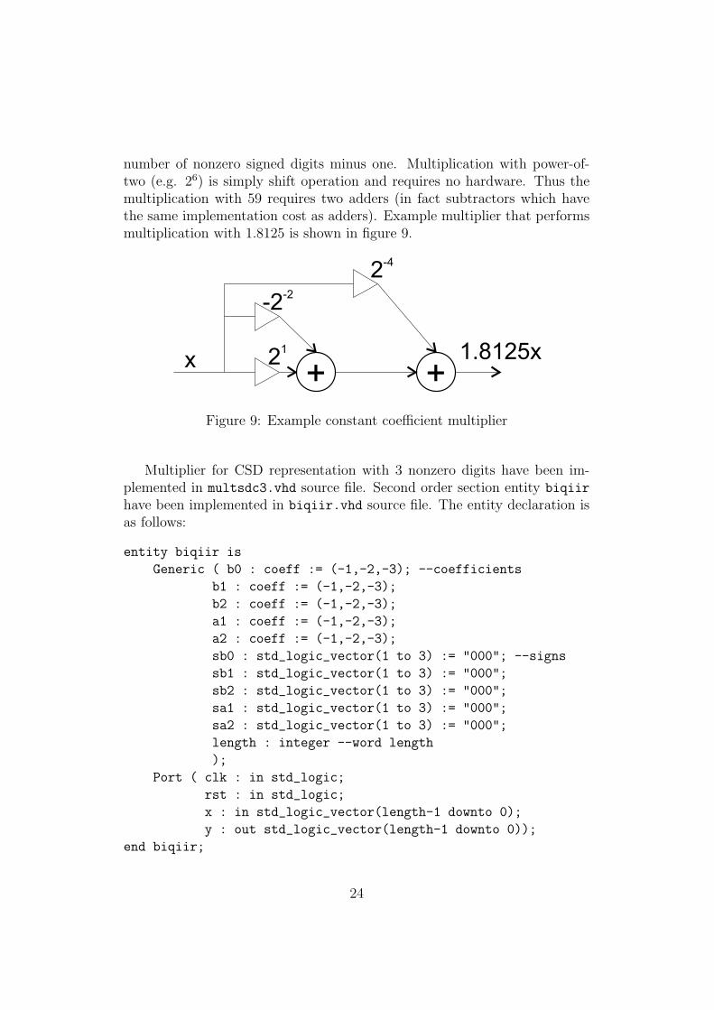
number of nonzero signed digits minus one. Multiplication with power-of-two (e.g. 26) is simply shift operation and requires no hardware. Thus themultiplication with 59 requires two adders (in fact subtractors which havethe same implementation cost as adders). Example multiplier that performsmultiplication with 1.8125 is shown in figure 9.
+ +
-2-2
2-4
x 1.8125x21
Figure 9: Example constant coefficient multiplier
Multiplier for CSD representation with 3 nonzero digits have been im-plemented in multsdc3.vhd source file. Second order section entity biqiir
have been implemented in biqiir.vhd source file. The entity declaration isas follows:
entity biqiir is
Generic ( b0 : coeff := (-1,-2,-3); --coefficients
b1 : coeff := (-1,-2,-3);
b2 : coeff := (-1,-2,-3);
a1 : coeff := (-1,-2,-3);
a2 : coeff := (-1,-2,-3);
sb0 : std_logic_vector(1 to 3) := "000"; --signs
sb1 : std_logic_vector(1 to 3) := "000";
sb2 : std_logic_vector(1 to 3) := "000";
sa1 : std_logic_vector(1 to 3) := "000";
sa2 : std_logic_vector(1 to 3) := "000";
length : integer --word length
);
Port ( clk : in std_logic;
rst : in std_logic;
x : in std_logic_vector(length-1 downto 0);
y : out std_logic_vector(length-1 downto 0));
end biqiir;
24
Type coeff – declared in iir pack.vhd package – is 3-element integertable for exponents of nonzero digits storing. Signs of this digits (1 means”minus”, 0 – ”plus”) are stored in 3-element std logic vector (sb0...sa1generics).
Preparations
• Calculate coefficients of IIR filter that meets specifications given inadvance. Factorize obtained transfer function into the cascade secondorder sections form.
• Quantize all coefficients of second order sections into the nearest CSDrepresentation with 3 nonzero digits. It can be done using Matlabsptconv.m script that is available for students. Write down exponentsand signs of nonzero digits.
Assignments
• Create a new ISE project. Add to the project: iir pack.vhd packagefile, multsdc3.vhd multiplier source file and biqiir.vhd second ordersection source file.
• Create a new VHDL source for the top level entity description. Declarebiqiir component and instantiate appropriate number of sections forthe filter. Coefficients shall be declared as generics.
• Compile the project and download into the board. Test if it worksusing sine generator and oscilloscope.
• To allow frequency response measurement by spectrum analyzer, changefilter clock frequency to 100kHz.
• Measure the frequency response of filter using spectrum analyzer. Savedata into floppy disc.
Report
• Create report including magnitude and phase response of the designedfilter measured by spectrum analyzer.
25
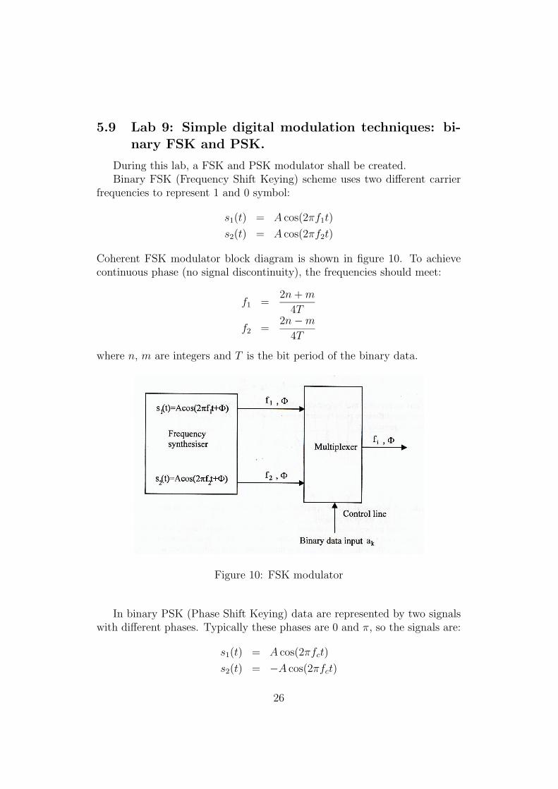
5.9 Lab 9: Simple digital modulation techniques: bi-nary FSK and PSK.
During this lab, a FSK and PSK modulator shall be created.Binary FSK (Frequency Shift Keying) scheme uses two different carrier
frequencies to represent 1 and 0 symbol:
s1(t) = A cos(2πf1t)
s2(t) = A cos(2πf2t)
Coherent FSK modulator block diagram is shown in figure 10. To achievecontinuous phase (no signal discontinuity), the frequencies should meet:
f1 =2n + m
4T
f2 =2n − m
4T
where n, m are integers and T is the bit period of the binary data.
Figure 10: FSK modulator
In binary PSK (Phase Shift Keying) data are represented by two signalswith different phases. Typically these phases are 0 and π, so the signals are:
s1(t) = A cos(2πfct)
s2(t) = −A cos(2πfct)
26

One signal represents 0 and the other – 1.
Assignments
• Design binary FSK modulator. Carrier frequencies should meet rela-tionships given above. The bit period will be given during the lab.
• Modulator shall send periodically 4 bits that are set on the DipSwitchon the development board. Observe the FSK signal and its spectrumon the scope.
• Design binary PSK modulator that periodically sends 4 bits. Observethe generated signal.
27
References[1] Memec Spartan-3 LC User’s Guide
[2] P160 Analog Module User Guide
[3] Spartan-3 FPGA Family: Complete Data Sheet
[4] Spartan-3 supported design elements, http://toolbox.xilinx.com/docsan/xilinx6/books/data/docs/lib/lib0022 8.html
[5] Using Block RAM in Spartan-3 FPGAs
[6] Using Embedded Multipliers in Spartan-3 FPGAs
[7] Using the ISE Design Tools for Spartan-3 FPGAs
[8] Using Spartan-3 IP Cores
[9] VHDL language guide, http://www.acc-eda.com/vhdlref/
[10] P.J. Ashenden The VHDL Cookbook
References are available on http://alfa.iele.polsl.gliwice.pl/∼wojsu/
28