Embed Size (px)
Citation preview
PRZEGLĄD ELEKTROTECHNICZNY (Electrical Review), ISSN 0033-2097, R. 87 NR 8/2011 187
Zbigniew HAJDUK1, Jan SADOLEWSKI1, Bartosz TRYBUS1
Rzeszow University of Technology, Faculty of Electrical and Computer Engineering, Department of Computer and Control Engineering (1)
FPGA-based Execution Platform for IEC 61131-3 Control Software
Streszczenie. W artykule przedstawiono platformę sprzętową opartą na technologii FPGA do wykonywania programów systemów sterowania tworzonych w językach normy IEC 61131-3 w zintegrowanym środowisku programistyczno-uruchomieniowym CPDev. Przedstawiono obsługiwane typy danych, kompilację do kodu pośredniego oraz dwie realizacje sprzętowej maszyny wykonawczej – podstawową i rozszerzoną. Realizacje poddano testom szybkości i porównano z maszynami programowymi obsługiwanymi przez CPDev. (Platforma wykonawcza FPGA dla systemów sterowania zgodnych z normą IEC 61131-3). Abstract. The article presents FPGA-based hardware platform for executing control system software written in languages of IEC 61131-3 standard in CPDev integrated development environment. Supported data types, compilation to intermediate code and two implementations of FPGA execution machine – basic and enhanced are described. The implementations have been tested for speed and compared with software-based platforms of CPDev package. Słowa kluczowe: FPGA, programowanie IEC 61131-3, CPDev, sterowniki PLCA. Keywords: FPGA, IEC 61131-3 programming, CPDev, PLC controllers. Introduction CPDev (Control Program Developer) is an open engineering environment [6] providing universal set of tools for developing of programmable controller software according to IEC 61131-3 standard [1]. ST language compiler (Structured Text), which produces universal executable code is the main component of the environment. The universal code is portable and executed on the controller side by the virtual machine, being a program written in ANSI C and compiled for particular hardware platform. Such solution provides portability and easy reconfiguration of the target controller. However, long interpretation time of the universal code is important drawback, at least several times longer than in case of the program written in assembly language. It is also hard to estimate execution cycle time, often adjusted by trial and error method. One can greatly reduce execution time of the universal code by replacing software-implemented virtual machine
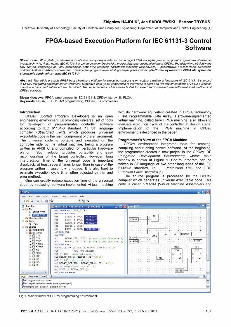
with its hardware equivalent created in FPGA technology (Field Programmable Gate Array). Hardware-implemented virtual machine, called here FPGA machine, also allows to evaluate execution cycle of the controller at design stage. Implementation of the FPGA machine in CPDev environment is described in the paper. Programmer’s View of the FPGA Machine CPDev environment integrates tools for creating, compiling and running control software. At the beginning, the programmer creates a new project in the CPDev IDE (Integrated Development Environment), whose main window is shown at Figure 1. Control program can be written in ST language or two other languages of the IEC 61131-3 standard, i.e. IL (Instruction List) and FBD (Function Block Diagram) [1]. The source program is processed by the CPDev compiler which generates universal executable code. This code is called VMASM (Virtual Machine Assembler) and
Fig.1. Main window of CPDev programming environment
188 PRZEGLĄD ELEKTROTECHNICZNY (Electrical Review), ISSN 0033-2097, R. 87 NR 8/2011
can be executed by the virtual machine. The virtual machine concept has been introduced into CPDev due to following reasons:
– providing common execution layer for programs written in different IEC languages,
– easy adaptation of various hardware platforms (microprocessors) for CPDev environment.
Virtual machine must be implemented in particular target platform to execute the VMASM code. So far, software-implemented machines written in C have been used in SMC controller [7], Mini-Guard ship monitoring system [5] and CPCtrl – PC soft-controller [8]. Several CPUs are supported, i.e. AVR and ARM microcontrollers, x86 processor, as well as popular operating systems (Windows, QNX, Windows CE .NET). Table 1. Elementary data types and VM implementation
Name Implementation Name Implementation BOOL 1B (0, 1) LINT 8B (-263 .. 263-1) SINT 1B (-128 .. 127) LWORD 8B (0 .. 264-1) BYTE 1B (0 .. 255) LREAL 8B (IEEE-754) INT 2B (-32768 .. 32767) DATE 4B WORD 2B (0 .. 65536) TIME_OF_DAY 4B DINT 4B (-231 .. 231-1) DATE_AND_TIME 8B DWORD 4B (0 .. 232-1) TIME 4B REAL 4B (IEEE-754) STRING Variable length string
The FPGA version of the virtual machine has been designed assuming that it must conform with existing VMASM specification of the software machine [9]. This will allow for reuse of already created control solutions, including libraries of function blocks. The functional side of the machine covers the following capabilities:
– Handling IEC data types: Boolean BOOL, integer BYTE, SINT, INT, WORD, DINT, LINT, DWORD, LWORD, real REAL, LREAL, time and date TIME, DATE, TIME_OF_DAY, DATE_AND_TIME; Table1 presents VM implementations of these types.
– Execution of functions (examples): arithmetic ADD, SUB, MUL, DIV, MOD, numerical SQRT, LOG, SIN, ASIN, EXP, Boolean NOT, AND, OR, XOR, bit shift SHL, ROL, comparison GT, GE, LT, EQ and others.
– Program flow control by means of jumps JMP, JZ, JNZ, calls of function block CALB and function CALF, early exit RETURN, memory handling MCD, MEMCP (Move from Code to Data, Memory Copy).
Basic logical registers of VM are listed in Table 2. Since accumulator does not exist in VM specification, results of commands are stored in variables. Task cycle can be configured and monitored by the machine during program execution. Actual task cycle (last value) is particularly useful for on-line testing (commissioning). Status1 stores exception flags, including cycle overflow, therefore appropriate reaction can be programmed. Design and Implementation of FPGA Machine The FPGA machine is actually a 32-bit microcontroller [2] that executes universal code VMASM generated in CPDev environment. The microcontroller is built according to Harvard architecture with separated data and program busses. To become more familiar with what the machine actually does, translation of STARTSTOP program written in ST language into VMASM is presented in Table 3 (compare Fig.1). First part of the ST code, from VAR_EXTERNAL declares the use of global variables. Local declarations VAR of the timer block instances DELAY_ON, DELAY_OFF are the second part. Program body consists of four statements, where the first one turns MOTOR on if START
is pressed, provided that STOP and ALARM are not set. MOTOR continues running after releasing START. Next three statements turn PUMP on and off by the two timers, 5 seconds after the MOTOR (PT:=t#5s). Table 2. Logical registers of FPGA machine
Register name Function Program counter Indicates next VMASM command Data offset Index to data area being used Call stack pointer Data stack pointer
Pointers to call stack (POUs) and data stack
Task cycle Actual task cycle
Configured and measured task cycle
Cycle counter Counts cycles (from reset)
Status1 VM status word (array index faulty, time cycle exceeded, cold start, etc.)
RTC clock Absolute time Table 3. ST program and its VMASM translation
Execution of the first VMASM instruction begins with testing values of START and MOTOR. If they are nonzero, JNZ jumps to :?OR0046 label, where MCD command sets ?LR?AND0045 variable (temporary) to 1 (#01). Otherwise ?LR?AND0045 is set to 0, followed by JMP to :?EOR004A. Then, if ?LR?AND0045 is nonzero, NOT, JZ and MCD set another ?LR?AND0043 variable to 0, provided that STOP is 1. In such case the first JZ on the right side of Table 3 jumps to :?AND0042, where MCD sets MOTOR to 0. If
ST program PROGRAM STARTSTOP VAR_EXTERNAL START : BOOL (*$READ*); STOP : BOOL (*$READ*); ALARM : BOOL (*$READ*); MOTOR : BOOL; PUMP : BOOL (*$WRITE*); END_VAR VAR DELAY_ON : TON; (* TON block instance *) DELAY_OFF: TOF; (* TOF block instance *) END_VAR MOTOR := (START OR MOTOR) AND NOT STOP AND NOT ALARM; (* TON - delayed start *) DELAY_ON(IN:=MOTOR, PT:=t#5s); (* TOF - delayed stop *) DELAY_OFF(IN:= DELAY_ON.Q, PT:=t#5s); (* Pump on/off state *) PUMP := DELAY_OFF.Q; END_PROGRAM
VMASM code JNZ START, :?OR0046 JNZ MOTOR, :?OR0046 MCD ?LR?AND0045, #01, #00 JMP :?EOR004A :?OR0046 MCD ?LR?AND0045, #01, #01 :?EOR004A JZ ?LR?AND0045, :?AND0044 NOT ?LR?AND004B, STOP JZ ?LR?AND004B, :?AND0044 MCD ?LR?AND0043, #01, #01 JMP :?EAND004E :? AND0044 MCD ?LR?AND0043, #01, #00
:?EAND004E JZ ?LR?AND0043, :?AND0042 NOT ?LR?AND004F, ALARM JZ ?LR?AND004F, :?AND0042 MCD MOTOR, #01, #01 JMP :?EAND0052 :?AND0042 MCD MOTOR, #01, #00 :?EAND0052 MEMCP DELAY_ON.IN, MOTOR, #0100 MCD DELAY_ON.PT, #04, #88130000 CALB DELAY_ON, :?TON?CODE MEMCP DELAY_OFF.IN, DELAY_ON.Q, #0100 MCD DELAY_OFF.PT, #04, #88130000 CALB DELAY_OFF, :?TOF?CODE MEMCP PUMP, DELAY_OFF.Q, #0100
PRZEGLĄD ELEKTROTECHNICZNY (Electrical Review), ISSN 0033-2097, R. 87 NR 8/2011 189
PROGRAM COUNTER (PC)
STACK
PMR
PROGRAM MEMORY READOUT CONTROL
REGISTERS
DMCDATA MEMORY ACCESS
CONTROL
DATA MEMORY(BLOCK RAM)
ADDR DI DO WE
ADDR DO DI WE
DA
TA
PO
INT
ER
ST
AC
K
88
16
REGISTERS
vDW
1vD
W2
32
32
IDC
INSTRUCTION DECODER WITH MAIN CONTROL
CIRCUIT
INSTRUCTION REGISTER
16
8
ALU
DATA
ADDRESS
PR
OG
RA
M M
EM
OR
Y
INT
ER
FA
CE
NATIVE FUNCTION BLOCK INTERFACE
INPUT/OUTPUT INTERFACE
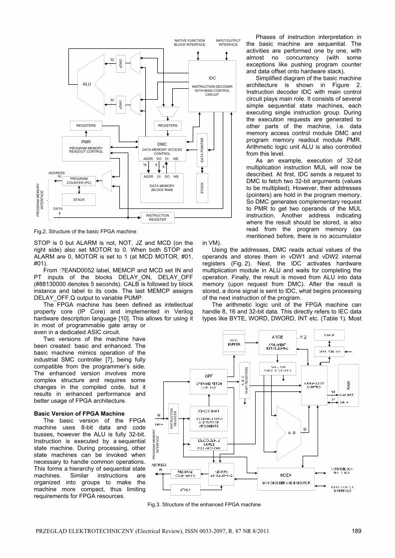
Fig.2. Structure of the basic FPGA machine
STOP is 0 but ALARM is not, NOT, JZ and MCD (on the right side) also set MOTOR to 0. When both STOP and ALARM are 0, MOTOR is set to 1 (at MCD MOTOR, #01, #01). From :?EAND0052 label, MEMCP and MCD set IN and PT inputs of the blocks DELAY_ON, DELAY_OFF (#88130000 denotes 5 seconds). CALB is followed by block instance and label to its code. The last MEMCP assigns DELAY_OFF.Q output to variable PUMP. The FPGA machine has been defined as intellectual property core (IP Core) and implemented in Verilog hardware description language [10]. This allows for using it in most of programmable gate array or even in a dedicated ASIC circuit. Two versions of the machine have been created: basic and enhanced. The basic machine mimics operation of the industrial SMC controller [7], being fully compatible from the programmer’s side. The enhanced version involves more complex structure and requires some changes in the compiled code, but it results in enhanced performance and better usage of FPGA architecture. Basic Version of FPGA Machine The basic version of the FPGA machine uses 8-bit data and code busses, however the ALU is fully 32-bit. Instruction is executed by a sequential state machine. During processing, other state machines can be invoked when necessary to handle common operations. This forms a hierarchy of sequential state machines. Similar instructions are organized into groups to make the machine more compact, thus limiting requirements for FPGA resources.
Phases of instruction interpretation in the basic machine are sequential. The activities are performed one by one, with almost no concurrency (with some exceptions like pushing program counter and data offset onto hardware stack). Simplified diagram of the basic machine architecture is shown in Figure 2. Instruction decoder IDC with main control circuit plays main role. It consists of several simple sequential state machines, each executing single instruction group. During the execution requests are generated to other parts of the machine, i.e. data memory access control module DMC and program memory readout module PMR. Arithmetic logic unit ALU is also controlled from this level. As an example, execution of 32-bit multiplication instruction MUL will now be described. At first, IDC sends a request to DMC to fetch two 32-bit arguments (values to be multiplied). However, their addresses (pointers) are hold in the program memory. So DMC generates complementary request to PMR to get two operands of the MUL instruction. Another address indicating where the result should be stored, is also read from the program memory (as mentioned before, there is no accumulator
in VM). Using the addresses, DMC reads actual values of the operands and stores them in vDW1 and vDW2 internal registers (Fig. 2). Next, the IDC activates hardware multiplication module in ALU and waits for completing the operation. Finally, the result is moved from ALU into data memory (upon request from DMC). After the result is stored, a done signal is sent to IDC, what begins processing of the next instruction of the program. The arithmetic logic unit of the FPGA machine can handle 8, 16 and 32-bit data. This directly refers to IEC data types like BYTE, WORD, DWORD, INT etc. (Table 1). Most
INS
TR
UC
TIO
N
RE
GIS
TE
R
A, B
, C16
-BIT
RE
GIS
TE
RS
RA
M
PR
OG
RA
M M
EM
OR
Y
INT
ER
FA
CE
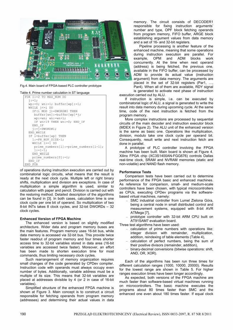
Fig.3. Structure of the enhanced FPGA machine
190 PRZEGLĄD ELEKTROTECHNICZNY (Electrical Review), ISSN 0033-2097, R. 87 NR 8/2011
of operations during instruction execution are carried out by combinatorial logic circuits, what means that the result is ready at the next clock cycle. Multiple left or right binary shifts, multiplication and division are exceptions. In case of multiplication a simple algorithm is used, similar to calculation with paper and pencil. Division is carried out with the restoring method. Detailed description of the algorithms can be found in [3]. In both cases, calculation time is one clock cycle per one bit of operand. So multiplication of two 8-bit INTs takes 8 clock cycles, and 32-bit DWORDs – 32 clock cycles. Enhanced Version of FPGA Machine The enhanced version is based on slightly modified architecture. Wider data and program memory buses are the main features. Program memory uses 16-bit bus, while data memory is accessed via 32-bit bus. This provide twice faster readout of program memory and four times shorter access time to 32-bit variables stored in data area (16-bit variables are accessed twice faster). Moreover, an effort has been made to shorten execution time for most commands, thus limiting necessary clock cycles. Such rearrangement of memory organization requires small changes of the code generated by CPDev compiler. Instruction code with operands must always occupy even number of bytes. Additionally, variable address must be a multiple of its size. This means that 32-bit variables are placed at addresses divisible by 4 (or 2 in case of 16-bit variables). Simplified structure of the enhanced FPGA machine is shown at Figure 3. Main concept is to construct a circuit responsible for fetching operands from program memory (addresses) and determining their actual values in data
memory. The circuit consists of DECODER1 responsible for fixing instruction arguments’ number and type, OPF block fetching operands from program memory, FIFO buffer, ARGE block establishing argument values from data memory and a set of 16- and 32-bit registers. Pipeline processing is another feature of the enhanced machine, meaning that some operations during instruction execution are parallel. For example, OPM and ADM blocks work concurrently. At the time when next operand (address) is being fetched, the previous one, available in the FIFO buffer, can be processed by ADM to provide its actual value (instruction argument) from data memory. The arguments are placed in the set of 32-bit registers (Par1, …, Par4). When all of them are available, RDY signal is generated to activate next phase of instruction
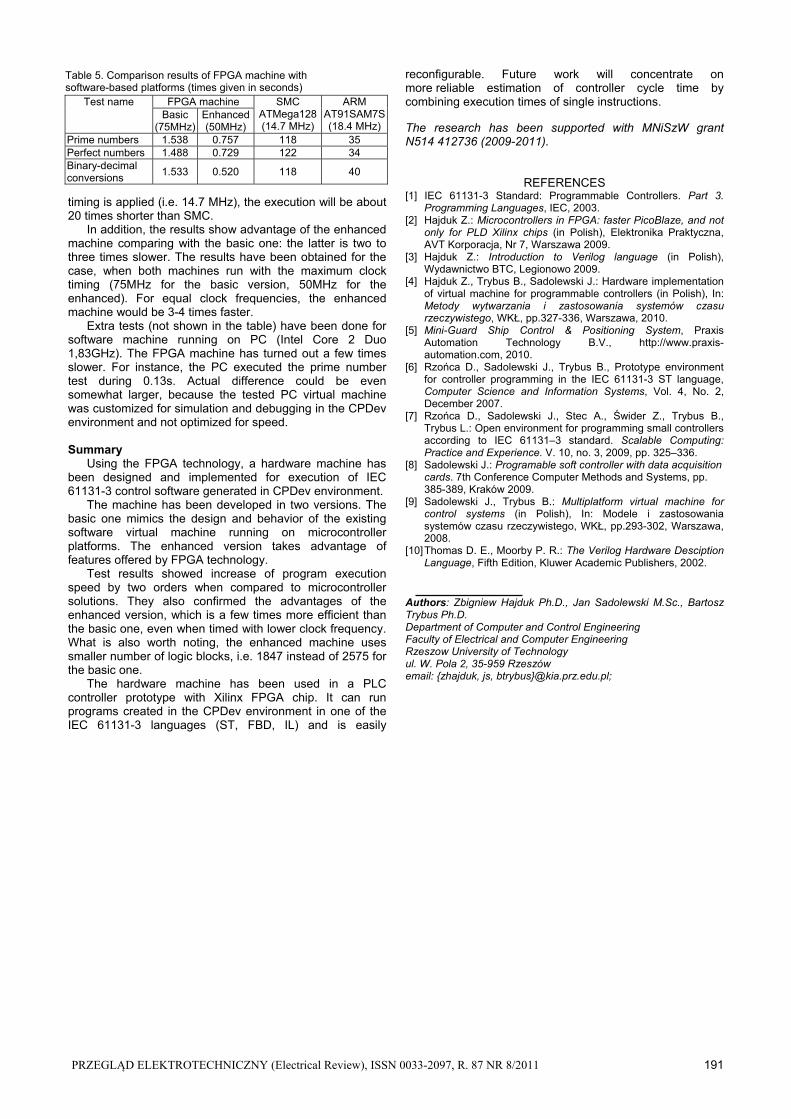
execution carried out by ALU. If instruction is simple, i.e. can be executed by combinatorial logic of ALU, a signal is generated to write the result into data memory during upcoming cycle. At the same time, code of the next instruction is fetched from the program memory. More complex instructions are processed by sequential circuits of the main decoder and instruction executor block (MDEX in Figure 2). The ALU unit of the enhanced version is the same as basic one. Operations like multiplication, division, modulo take one clock cycle per operand bit. Consequently, result write and next instruction fetch are done in parallel. A prototype of PLC controller involving the FPGA machine has been built. Main board is shown at Figure 4. Xilinx FPGA chip (XC3S1400AN-FGG676) controls Dallas real-time clock, SRAM and NVRAM memories (static and non-volatile) and NAND flash memory. Performance Tests Comparison tests have been carried out to determine performance of the FPGA basic and enhanced machines. As reference for comparison, small- and medium-scale controllers have been chosen, with typical microcontrollers as CPUs, executing CPDev programs via the software-based virtual machines, namely:
– SMC industrial controller from Lumel Zielona Góra, being a central node in small distributed control and measurement systems, equipped with 8-bit AVR ATMega [7],
– prototype controller with 32-bit ARM CPU built on AT91SAM7 evaluation board.
Three test algorithms have been used: – calculation of prime numbers with operations like:
integer division with remainder, multiplication, addition, reindexing of table elements (Table 4),
– calculation of perfect numbers, being the sum of their positive divisors (remainder, addition),
– binary-decimal conversions (bitwise operations: shift, AND, OR, XOR).
Each of the algorithms has been run three times for different calculation ranges (1000, 10000, 20000). Results for the lowest range are shown in Table 5. For higher ranges execution times have been longer accordingly. As expected, both versions of the FPGA machine are much faster than software-based virtual machines running on microcontrollers. The basic machine executes the programs about 80 times faster than SMC and the enhanced one even about 180 times faster. If equal clock
Fig.4. Main board of FPGA-based PLC controller prototype
Table 4. Prime number calculation in ST language
FOR i:=2 TO MAX_NUM DO j:=1; wp:=0; wn:=1; buffer[wp]:=1; WHILE j<=i DO IF(i MOD j)=DWORD#0 THEN buffer[wn]:=buffer[wp]*j; wp:=wn; wn:=wn+1; IF wn>19 THEN wn:=0; END_IF END_IF j:=j+DWORD#1; END_WHILE IF i=buffer[wp] THEN l:=PN_BUF_SIZE-1; WHILE l>=1 DO prime_numbers[l]:=prime_numbers[l-1]; l:=l-1; END_WHILE prime_numbers[0]:=i; END_IF END_FOR
PRZEGLĄD ELEKTROTECHNICZNY (Electrical Review), ISSN 0033-2097, R. 87 NR 8/2011 191
timing is applied (i.e. 14.7 MHz), the execution will be about 20 times shorter than SMC. In addition, the results show advantage of the enhanced machine comparing with the basic one: the latter is two to three times slower. The results have been obtained for the case, when both machines run with the maximum clock timing (75MHz for the basic version, 50MHz for the enhanced). For equal clock frequencies, the enhanced machine would be 3-4 times faster. Extra tests (not shown in the table) have been done for software machine running on PC (Intel Core 2 Duo 1,83GHz). The FPGA machine has turned out a few times slower. For instance, the PC executed the prime number test during 0.13s. Actual difference could be even somewhat larger, because the tested PC virtual machine was customized for simulation and debugging in the CPDev environment and not optimized for speed. Summary Using the FPGA technology, a hardware machine has been designed and implemented for execution of IEC 61131-3 control software generated in CPDev environment. The machine has been developed in two versions. The basic one mimics the design and behavior of the existing software virtual machine running on microcontroller platforms. The enhanced version takes advantage of features offered by FPGA technology. Test results showed increase of program execution speed by two orders when compared to microcontroller solutions. They also confirmed the advantages of the enhanced version, which is a few times more efficient than the basic one, even when timed with lower clock frequency. What is also worth noting, the enhanced machine uses smaller number of logic blocks, i.e. 1847 instead of 2575 for the basic one. The hardware machine has been used in a PLC controller prototype with Xilinx FPGA chip. It can run programs created in the CPDev environment in one of the IEC 61131-3 languages (ST, FBD, IL) and is easily
reconfigurable. Future work will concentrate on more reliable estimation of controller cycle time by combining execution times of single instructions. The research has been supported with MNiSzW grant N514 412736 (2009-2011).
REFERENCES [1] IEC 61131-3 Standard: Programmable Controllers. Part 3.
Programming Languages, IEC, 2003. [2] Hajduk Z.: Microcontrollers in FPGA: faster PicoBlaze, and not
only for PLD Xilinx chips (in Polish), Elektronika Praktyczna, AVT Korporacja, Nr 7, Warszawa 2009.
[3] Hajduk Z.: Introduction to Verilog language (in Polish), Wydawnictwo BTC, Legionowo 2009.
[4] Hajduk Z., Trybus B., Sadolewski J.: Hardware implementation of virtual machine for programmable controllers (in Polish), In: Metody wytwarzania i zastosowania systemów czasu rzeczywistego, WKŁ, pp.327-336, Warszawa, 2010.
[5] Mini-Guard Ship Control & Positioning System, Praxis Automation Technology B.V., http://www.praxis-automation.com, 2010.
[6] Rzońca D., Sadolewski J., Trybus B., Prototype environment for controller programming in the IEC 61131-3 ST language, Computer Science and Information Systems, Vol. 4, No. 2, December 2007.
[7] Rzońca D., Sadolewski J., Stec A., Świder Z., Trybus B., Trybus L.: Open environment for programming small controllers according to IEC 61131–3 standard. Scalable Computing: Practice and Experience. V. 10, no. 3, 2009, pp. 325–336.
[8] Sadolewski J.: Programable soft controller with data acquisition cards. 7th Conference Computer Methods and Systems, pp. 385-389, Kraków 2009.
[9] Sadolewski J., Trybus B.: Multiplatform virtual machine for control systems (in Polish), In: Modele i zastosowania systemów czasu rzeczywistego, WKŁ, pp.293-302, Warszawa, 2008.
[10] Thomas D. E., Moorby P. R.: The Verilog Hardware Desciption Language, Fifth Edition, Kluwer Academic Publishers, 2002.
Authors: Zbigniew Hajduk Ph.D., Jan Sadolewski M.Sc., Bartosz Trybus Ph.D. Department of Computer and Control Engineering Faculty of Electrical and Computer Engineering Rzeszow University of Technology ul. W. Pola 2, 35-959 Rzeszów email: {zhajduk, js, btrybus}@kia.prz.edu.pl;
Table 5. Comparison results of FPGA machine with software-based platforms (times given in seconds)
Test name FPGA machine SMC ATMega128 (14.7 MHz)
ARM AT91SAM7S(18.4 MHz)
Basic (75MHz)
Enhanced (50MHz)
Prime numbers 1.538 0.757 118 35 Perfect numbers 1.488 0.729 122 34 Binary-decimal conversions
1.533 0.520 118 40