Embed Size (px)
Citation preview

This article was downloaded by: [Oak Ridge National Laboratory], [Philip Evans]On: 05 September 2012, At: 11:57Publisher: Taylor & FrancisInforma Ltd Registered in England and Wales Registered Number: 1072954 Registered office: Mortimer House,37-41 Mortimer Street, London W1T 3JH, UK
Journal of Modern OpticsPublication details, including instructions for authors and subscription information:http://www.tandfonline.com/loi/tmop20
FPGA-based gating and logic for multichannel singlephoton countingRaphael C. Pooser a , Dennis D. Earl a , Philip G. Evans a , Brian Williams a b , Jason Schaakea b & Travis S. Humble ca Computational Sciences and Engineering Division, Oak Ridge National Laboratory, OakRidge, TN 37831, USAb Department of Physics, University of Tennessee, Knoxville, TN 37996, USAc Computational Science and Mathematics Division, Oak Ridge National Laboratory, OakRidge, TN 37831, USA
Version of record first published: 30 Jul 2012
To cite this article: Raphael C. Pooser, Dennis D. Earl, Philip G. Evans, Brian Williams, Jason Schaake & Travis S.Humble (2012): FPGA-based gating and logic for multichannel single photon counting, Journal of Modern Optics,DOI:10.1080/09500340.2012.706325
To link to this article: http://dx.doi.org/10.1080/09500340.2012.706325
PLEASE SCROLL DOWN FOR ARTICLE
Full terms and conditions of use: http://www.tandfonline.com/page/terms-and-conditions
This article may be used for research, teaching, and private study purposes. Any substantial or systematicreproduction, redistribution, reselling, loan, sub-licensing, systematic supply, or distribution in any form toanyone is expressly forbidden.
The publisher does not give any warranty express or implied or make any representation that the contentswill be complete or accurate or up to date. The accuracy of any instructions, formulae, and drug doses shouldbe independently verified with primary sources. The publisher shall not be liable for any loss, actions, claims,proceedings, demand, or costs or damages whatsoever or howsoever caused arising directly or indirectly inconnection with or arising out of the use of this material.
Journal of Modern Optics2012, 1–12, iFirst
FPGA-based gating and logic for multichannel single photon counting
Raphael C. Poosera*, Dennis D. Earla, Philip G. Evansa, Brian Williamsa,b,Jason Schaakea,b and Travis S. Humblec
aComputational Sciences and Engineering Division, Oak Ridge National Laboratory, Oak Ridge, TN 37831, USA;bDepartment of Physics, University of Tennessee, Knoxville, TN 37996, USA; cComputational Science and
Mathematics Division, Oak Ridge National Laboratory, Oak Ridge, TN 37831, USA
(Received 31 January 2012; final version received 19 June 2012)
We present results characterizing multichannel InGaAs single photon detectors utilizing gated passive quenchingcircuits (GPQC), self-differencing techniques, and field programmable gate array (FPGA)-based logic for bothdiode gating and coincidence counting. Utilizing FPGAs for the diode gating frontend and the logic countingbackend has the advantage of low cost compared to custom built logic circuits and current off-the-shelf detectortechnology. Further, FPGA logic counters have been shown to work well in quantum key distribution (QKD)test beds. Our setup combines multiple independent detector channels in a reconfigurable manner via an FPGAbackend and post processing in order to perform coincidence measurements between any two or more detectorchannels simultaneously. Using this method, states from a multi-photon polarization entangled source aredetected and characterized via coincidence counting on the FPGA. Photons detection events are also processedby the quantum information toolkit for application testing (QITKAT).
Keywords: optical instrumentation and technology; single photon detector; SPAD; multichannel photoncounting; FPGA coincidence logic
1. Introduction
Many applications which make use of photon counting
have traditionally relied on counting coincidences
between two photons, such as those produced by
spontaneous parametric downconversion [1–3].
Recently, multichannel photon counting with highspeed and accuracy has garnered great interest for a
wide variety of applications. For instance, recent
advances in quantum key distribution (QKD) net-
works have outlined the need for multichannel photon
signal processing [4]. A prime technology for multi-
channel coincidence counting is field programmable
gate array (FPGA) logic [5–7]. FPGAs are low cost,highly configurable, high speed signal processing
devices. They can be used to time stamp photon
arrival times by registering logic pulses, measure
coincidences using comparator circuits, and act as
gate circuits for detector operation. Combined with
single photon detectors utilizing gated passive quench-
ing circuits (GPQC) and self-differencing techniques,cheap high speed single photon detectors (SPDs) can
be constructed and used in multichannel configura-
tions. Here we present a SPD design based around
FPGA gating and counting logic and GPQCs. TheFPGA backend uses comparator circuits to registercoincidences between two detectors, and time stampingof photon arrival times to register multichannel coin-cidences. Here we outline both cases and compareFPGA logic to older purpose-built nuclear instrumen-tation module (NIM) coincidence electronics.
2. Twofold coincidence counter
Our first use of FPGAs involves implementing acoincidence logic counter. In certain scenarios, suchas real time monitoring of visibility over a fiber link, ahigh resolution picture of visibility without accidentalsubtraction is needed. In particular, a high accidentalcount leads to reduced confidence in these measure-ments if they are not subtracted out. By utilizing higherresolution FPGA counters in our experiments, visibil-ity is closer to ideal without post-processing.
Figure 1 shows a schematic of the setup for aFranson interference experiment, utilizing spectrallyentangled photon pairs. The goal of the experiment isreal-time monitoring of the visibility without the need
*Corresponding author. Email: [email protected]
ISSN 0950–0340 print/ISSN 1362–3044 onlineThis material is published by permission of Oak Ridge, operated by UT-Battelle for the US Department of Energy under Contract No. DE-AC05-00OR22725. The US Government retains foritself, and others acting on its behalf, a paid-up, non-exclusive, and irrevocable worldwide license in said article to reproduce, prepare derivative works, distribute copies to the public, andperform publicly and display publicly, by or on behalf of the Governmenthttp://dx.doi.org/10.1080/09500340.2012.706325http://www.tandfonline.com
Dow
nloa
ded
by [
Oak
Rid
ge N
atio
nal L
abor
ator
y], [
Phili
p E
vans
] at
11:
57 0
5 Se
ptem
ber
2012
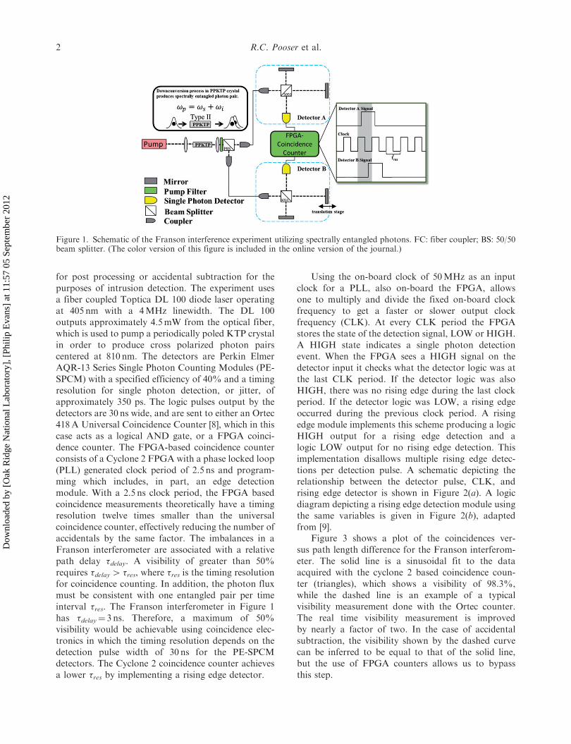
for post processing or accidental subtraction for thepurposes of intrusion detection. The experiment usesa fiber coupled Toptica DL 100 diode laser operatingat 405 nm with a 4MHz linewidth. The DL 100outputs approximately 4.5mW from the optical fiber,which is used to pump a periodically poled KTP crystalin order to produce cross polarized photon pairscentered at 810 nm. The detectors are Perkin ElmerAQR-13 Series Single Photon Counting Modules (PE-SPCM) with a specified efficiency of 40% and a timingresolution for single photon detection, or jitter, ofapproximately 350 ps. The logic pulses output by thedetectors are 30 ns wide, and are sent to either an Ortec418A Universal Coincidence Counter [8], which in thiscase acts as a logical AND gate, or a FPGA coinci-dence counter. The FPGA-based coincidence counterconsists of a Cyclone 2 FPGA with a phase locked loop(PLL) generated clock period of 2.5 ns and program-ming which includes, in part, an edge detectionmodule. With a 2.5 ns clock period, the FPGA basedcoincidence measurements theoretically have a timingresolution twelve times smaller than the universalcoincidence counter, effectively reducing the number ofaccidentals by the same factor. The imbalances in aFranson interferometer are associated with a relativepath delay �delay. A visibility of greater than 50%requires �delay4 �res, where �res is the timing resolutionfor coincidence counting. In addition, the photon fluxmust be consistent with one entangled pair per timeinterval �res. The Franson interferometer in Figure 1has �delay¼ 3 ns. Therefore, a maximum of 50%visibility would be achievable using coincidence elec-tronics in which the timing resolution depends on thedetection pulse width of 30 ns for the PE-SPCMdetectors. The Cyclone 2 coincidence counter achievesa lower �res by implementing a rising edge detector.
Using the on-board clock of 50MHz as an inputclock for a PLL, also on-board the FPGA, allowsone to multiply and divide the fixed on-board clockfrequency to get a faster or slower output clockfrequency (CLK). At every CLK period the FPGAstores the state of the detection signal, LOW or HIGH.A HIGH state indicates a single photon detectionevent. When the FPGA sees a HIGH signal on thedetector input it checks what the detector logic was atthe last CLK period. If the detector logic was alsoHIGH, there was no rising edge during the last clockperiod. If the detector logic was LOW, a rising edgeoccurred during the previous clock period. A risingedge module implements this scheme producing a logicHIGH output for a rising edge detection and alogic LOW output for no rising edge detection. Thisimplementation disallows multiple rising edge detec-tions per detection pulse. A schematic depicting therelationship between the detector pulse, CLK, andrising edge detector is shown in Figure 2(a). A logicdiagram depicting a rising edge detection module usingthe same variables is given in Figure 2(b), adaptedfrom [9].
Figure 3 shows a plot of the coincidences ver-sus path length difference for the Franson interferom-eter. The solid line is a sinusoidal fit to the dataacquired with the cyclone 2 based coincidence coun-ter (triangles), which shows a visibility of 98.3%,while the dashed line is an example of a typicalvisibility measurement done with the Ortec counter.The real time visibility measurement is improvedby nearly a factor of two. In the case of accidentalsubtraction, the visibility shown by the dashed curvecan be inferred to be equal to that of the solid line,but the use of FPGA counters allows us to bypassthis step.
Figure 1. Schematic of the Franson interference experiment utilizing spectrally entangled photons. FC: fiber coupler; BS: 50/50beam splitter. (The color version of this figure is included in the online version of the journal.)
2 R.C. Pooser et al.
Dow
nloa
ded
by [
Oak
Rid
ge N
atio
nal L
abor
ator
y], [
Phili
p E
vans
] at
11:
57 0
5 Se
ptem
ber
2012

The timing resolution of the detector and coinci-
dence electronics was verified by detecting uncorre-
lated photons and counting the coincidences. The
timing resolution �res is given by:
�res ¼TCconic
CACB
where T is the count time, Ccoinc is the number of
coincidences counted in time T, CA is the number
of raw counts from detector A in time T, and CB is thenumber of raw counts from detector B in time T.To determine the actual timing resolution of the FPGAbased coincidence counter we used two PE-SPCMsto detect photons from the room lights in our lab,which are uncorrelated. Table 1 below summarizesthe results.
The measured timing resolutions for both theFPGA and Ortec418A approximately agree with theexpected timing resolutions.
Figure 2. (a) Schematic showing the generation of a rising edge logic pulse upon detection of a high logic level on the detectorinput port. (b) A schematic which shows the basic function of the VHDL code used to configure the FPGA. (The color version ofthis figure is included in the online version of the journal.)
Figure 3. Coincidences (triangles) as a function of path length difference. The solid (red) line shows a sinusoidal fit to the dataobtained using FPGA coincidence counters, while the dashed (green) line shows a typical visibility obtained with the Orteccounter. (The color version of this figure is included in the online version of the journal.)
Journal of Modern Optics 3
Dow
nloa
ded
by [
Oak
Rid
ge N
atio
nal L
abor
ator
y], [
Phili
p E
vans
] at
11:
57 0
5 Se
ptem
ber
2012

The supplementary online material (see Figure S1)shows an example of the VHDL code written to detectcoincidences with the cyclone II FPGA, configuredin QUARTUS II 8.0. The code was modified fromexample code provided in [9]. A photo of the customFPGA board is also included (see Figure S2 online).
3. FPGA gating for single photon avalanche
diodes (SPADs)
Previous work has shown that GPQCs can utilize bothsinusoidal shaped [10–13] and square shaped [14–19]gate pulses. In addition, both methods can be usedwith self-differencing circuits in order to remove thediode capacitive response [19,20]. Here we use anFPGA with a configurable PLL as the gate source.The Stratix II FPGA has a PLL which is capableof reaching the 76MHz repetition rate of the mode-locked coherent Mira Ti:sapphire laser used in ourexperiments and multiples thereof.
The nominal shape of the PLL output is a squarewave when properly impedance matched. Sharp cor-ners in the wire traces on the FPGA circuit board actas low pass filters, reducing the shape from a squarewave to a rounded peak with smoothed corners.However, rounded pulse shapes are not necessarilya detraction in certain cases. For instance, the self-differencing circuit that is used to subtract the diode’scapacitive response has a set bandwidth over which itwill work reliably. A pure square wave has many highfrequency components (seen in the Fourier series),some of which may fall outside the bandwidth of theself-differencing circuit. This leads to higher amplituderesidual ripples in the difference signal than with apure sine wave gate. Depending on the quality of thedifferencing circuit, the ripples in some cases could belarge enough to mask the avalanche, thereby defeatingthe purpose. In these scenarios applying a low passfilter to the gate can help in recovering the signal bymoving the diode response into the difference circuit’sbandwidth. Previous experimental results have shownthe benefit of filtering the gate pulse [19]. To obtaina sine wave gate from such signals, a low pass filter atthe frequency of interest can be placed on the outputof the PLL. A 90MHz 3dB corner low pass filter canbe used to obtain a 76MHz sine wave from the
PLL when set to output a 76MHz square wave, forinstance. The same method can be used for highermultiples, 152MHz and 228MHz. In this way, we canachieve approximate square wave gates or sine wavegates for driving a diode using the FPGA PLL.
Our self-difference circuit is designed for 76MHz.It also takes the difference of multiples, but eachharmonic is subtracted less efficiently, since subsequentharmonics contain higher frequency components thanthe last. A sine wave gate alleviates many of theproblems associated with square wave gates in the self-differencing circuit, but introduces other downsides,such as non-uniform detection efficiency during thegate pulse. Further, dark counts increase over what asquare gate source would allow due to the increasedtime spent above breakdown voltage for a givenovervoltage setting [21,22]. Figure 4 shows an exampleof this effect. To alleviate this problem, the frequencyof the sine wave can be increased, reducing the amountof time spent above breakdown per gate, but increasingthe number of gates per second. In order to reduce thenumber of gates per second, but keep the smoothcorners of a sine wave, a blanking signal can be used.On the other hand, this leads to the same idea as
Figure 4. Oscilloscope trace (scope bandwidth: 300MHz)of a sinusoidal gate pulse with 152MHz period. Thehorizontal lines correspond to three cases of overvoltage.Dotted (blue) line: 2V over breakdown. Dashed (green): 1Vover breakdown. Dash-dotted (black): 0.5V above break-down. For each case, the amount of time spent abovebreakdown is noted. (The color version of this figure isincluded in the online version of the journal.)
Table 1. Measured timing resolution for Cyclone 2 coincidence counter and Ortec418A.
Device T A counts B counts Coincidences Measured �res Expected �res
Ortec418A 1000 s 12,858,367 12,243,910 5025 31.92 ns 30 nsFPGA 1000 s 12,911,963 12,263,055 418 2.64 ns 2.5 ns
4 R.C. Pooser et al.
Dow
nloa
ded
by [
Oak
Rid
ge N
atio
nal L
abor
ator
y], [
Phili
p E
vans
] at
11:
57 0
5 Se
ptem
ber
2012

previously mentioned: a square wave with roundededges, which can be obtained by shaping the outputimpedance of the FPGA PLL, as shown in Figure 5.While higher dark counts and lower quantum effi-ciency are downsides to this technique, expedience andlow cost are two upsides. Custom electronics for gatecircuits do not need to be developed if the FPGA PLLis acceptable for a given photon counting application.
In some cases, applying a low pass filter to theoutput of the self-difference circuit is also beneficial.Figure 6 shows a comparison of an avalanche pulsewith and without a DC-180MHz low pass filter afterthe self-differencing circuit, with a 152MHz, 3V peakto peak, 20% duty cycle square wave used as the gatepulse. The diode was driven approximately 2V abovebreakdown. In this case, the result is that the highfrequency ripples are attenuated while leaving most ofthe signal pulse. Figure 6 shows an increase in SNRof 80% at the expense of broadening the pulse byapproximately 50%. In general, however, the properlow pass filter will depend on the gate pulse length,overvoltage, and frequency. These factors would haveto be taken into account in order to ensure that theavalanche pulse itself is not also attenuated along withthe noise floor. An in depth study of these effects is thesubject of a future study.
Figure 7 shows a schematic of the entire detectordesign with the FPGA-based GPQC and self-differen-cing circuit. The inset of Figure 7 shows the output ofthe self-differencing circuit before and after differenc-ing with an avalanche event. After amplification by apair of minicircuits ZX60-4016 amplifiers [23], theavalanche pulse is sent to an ECL comparator
(On Semi MCE10E1652FNG) which outputs NIMlogic pulses, which are then converted to TTL using alevel translator or TTL comparator. Figure 8 shows anavalanche pulse and subsequent TTL pulse a fewnanoseconds later. The pulse was obtained by splittingthe analog signal before the ECL comparator. Half ofthe signal was sent to the oscilloscope and half was sentthe ECL-TTL network and then to the oscilloscope.The delay between the avalanche pulse and TTL pulsearises from cable length differences between the self-differencing circuit and the scope and comparators, aswell as intrinsic delay in the comparator network.While not quite 5V peak to peak, a signal of the typeshown in Figure 8 is readable by our FPGA countersand other logic units such as the Stanford ResearchSR620 [24].
3.1. Efficiency, dark counts, and afterpulsing
Our current detector design achieves 13% quantumefficiency with an overvoltage of 1.5V and a sinusoidalgate of 76MHz, 4.25V p-p, with an InGaAs diodefrom Princeton Lightwave (PL), model PGA-300.The detector is currently cooled to �46.9(9)�C, whichis limited by the temperature measurement device weuse rather than physical limits on the temperaturecontrol apparatus. The diode is placed in a20mm� 20mm heat sink, cooled by a Peltier element,and placed in a small plastic box (40mm3) filled withfoam insulation and desiccant.
The efficiency was measured using photons froma spontaneous parametric downconversion experimentwhich produces telecom photons centered at 1550 nm[25]. The counts per second (cps) were comparedwith the cps from a detector with known efficiency,the IdQuantique id-200 which is specified at 10%.The id-200 was gated at a rate of 4.757(9)MHzand was synchronized to a pulse obtained from theTi:sapphire pump laser (Coherent Mira) used in theSPDC experiment. The Mira has a repetition rateof 76.126(5)MHz, and the frequency was divided by16 using a Quantum Technology divide-by unit beforegating the id-200. Thus, at most, down convertedphotons synchronized with only one out of every 16laser pulses are detected by the id-200. To determine onaverage how many photons per second a detector gatedat the laser frequency would detect, the number mustbe multiplied by 16. When the PL diode was gated witha 76.126(5)MHz, 4.25V p-p sine wave, and driven1.5V above breakdown, the home made detectorregistered 1,180,000 cps versus 55,000 cps for theid-200, corresponding to an efficiency of 13.4� 0.4%.The dark counts at this efficiency were 45,000 cps for adiode temperature of �43�C. Using a Cyclone 4 as the
Figure 5. Oscilloscope trace (scope bandwidth: 300MHz)showing a gate pulse obtained from the FPGA PLL. Inset:close up of a single gate pulse. Note the diode is held belowbreakdown �0.5V in between the pulses such that the noisein the troughs would not contribute to avalanches. The dutycycle can be controlled by programming the PLL, here a 15%duty cycle was programmed. (The color version of this figureis included in the online version of the journal.)
Journal of Modern Optics 5
Dow
nloa
ded
by [
Oak
Rid
ge N
atio
nal L
abor
ator
y], [
Phili
p E
vans
] at
11:
57 0
5 Se
ptem
ber
2012

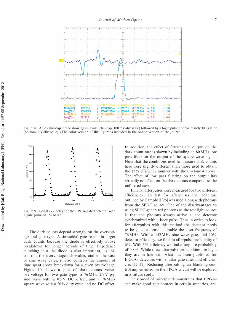
FPGA gate source allowed for a programmable delayin the gate pulse which was not possible with theStratix board. The delay had to be adjusted in order tooverlap the diode gates with incident light pulses.Currently, the Cyclone 4 based gate circuit is capableof a programmable gate delay with 100 ps resolution.The Mira laser pulses are 100 ps long, and the incidentdown converted photon pulses are of about the
same width. Thus, it is possible that the incidentphotons were not lined up exactly with the center of thegate pulse. A future version of the FPGA gate willinclude higher delay resolution in order to allow for amore accurate measurement of efficiency. The plot inFigure 9 below shows the effective width of a 200 pstiming resolution programmable delay on the detectedphoton pulse peaks.
Figure 6. Top: an avalanche after passing through a low pass filter at 180MHz. The corresponding gate pulse was 152MHz,2V above breakdown. Bottom: an avalanche pulse after passing through the self-differencing circuit and mini circuits mini-circuits ZX60-401E-Sþ amplifier without a low pass filter. (The color version of this figure is included in the online version of thejournal.)
Figure 7. A schematic of the gated passive quenching circuit. An FPGA is used as both the gate circuit and the counting logic.Inset: Top: oscilloscope trace of the capacitive response from each arm the self-differencing circuit, before recombination on thebalun. Bottom: the corresponding signal after subtraction at the balun revealing the avalanche pulse. Note: the top and bottomplots in the inset have different horizontal and vertical scales. (The color version of this figure is included in the online version ofthe journal.)
6 R.C. Pooser et al.
Dow
nloa
ded
by [
Oak
Rid
ge N
atio
nal L
abor
ator
y], [
Phili
p E
vans
] at
11:
57 0
5 Se
ptem
ber
2012
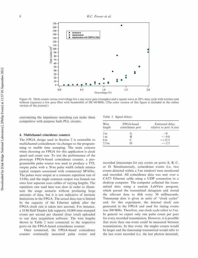
The dark counts depend strongly on the overvolt-age and gate type. A sinusoidal gate results in largerdark counts because the diode is effectively abovebreakdown for longer periods of time. Impedancematching into the diode is also important, as thiscontrols the overvoltage achievable, and in the caseof sine wave gates, it also controls the amount oftime spent above breakdown for a given overvoltage.Figure 10 shows a plot of dark counts versusovervoltage for two gate types: a 76MHz 2.9V p-psine wave with a 0.5V DC offset, and a 76MHzsquare wave with a 20% duty cycle and no DC offset.
In addition, the effect of filtering the output on the
dark count rate is shown by including an 80MHz low
pass filter on the output of the square wave signal.
Note that the conditions used to measure dark counts
here were slightly different than those used to obtain
the 13% efficiency number with the Cyclone 4 above.
The effect of low pass filtering on the output has
virtually no effect on the dark counts compared to the
unfiltered case.Finally, afterpulses were measured for two different
efficiencies. To test for afterpulses the technique
outlined by Campbell [26] was used along with photons
from the SPDC source. One of the disadvantages to
using SPDC-generated photons as the test light source
is that the photons always arrive at the detector
synchronized with a laser pulse. Thus in order to look
for afterpulses with this method the detector needs
to be gated at least at double the laser frequency of
76MHz. With a 152MHz sine wave gate, and 10%
detector efficiency, we find an afterpulse probability of
6%. With 3% efficiency we find afterpulse probability
of 0.8%. While these afterpulse probabilities are high,
they are in line with what has been published for
InGaAs detectors with similar gate rates and efficien-
cies [27–29]. Reducing afterpulsing via blanking con-
trol implemented on the FPGA circuit will be explored
in a future study.This proof of principle demonstrates that FPGAs
can make good gate sources in certain scenarios, and
Figure 8. An oscilloscope trace showing an avalanche (top, 100mV/div scale) followed by a logic pulse approximately 18 ns later(bottom, 1V/div scale). (The color version of this figure is included in the online version of the journal.)
Figure 9. Counts vs. delay for the FPGA-gated detector witha gate pulse of 152MHz.
Journal of Modern Optics 7
Dow
nloa
ded
by [
Oak
Rid
ge N
atio
nal L
abor
ator
y], [
Phili
p E
vans
] at
11:
57 0
5 Se
ptem
ber
2012
customizing the impedance matching can make themcompetitive with purpose built PLL circuits.
4. Multichannel coincidence counters
The FPGA design used in Section 2 is extensible tomultichannel coincidences via changes to the program-ming to enable time stamping. The main concernwhen choosing an FPGA for this application is clockspeed and count rate. To test the performance of theprototype FPGA-based coincidence counter, a pro-grammable pulse source was used to produce a TTLoutput pulse with a 50 ns pulse width (which mimicstypical outputs associated with commercial SPADs).The pulses were output at a constant repetition rate of5.0Hz, and the single common output was fanned outonto four separate coax cables of varying lengths. Therepetition rate used here was slow in order to illumi-nate the usage scenario without producing largeamounts of data, but it is not indicative of intrinsiclimitations in the FPGA. The actual data rate is limitedby the capacity of the Ethernet uplink after theFPGA clock rate is taken into account. For instance,a 10M/Half Duplex link supports 10,000 time-stampedevents per second per channel (four total) uploadedto our data acquisition software. The wire lengthsshown in Table 2 were connected to the respectiveports on the FPGA-based coincidence counter.
Once connected, the FPGA-based coincidencecounter continually measured pulse events and
recorded timestamps for any events on ports A, B, C,
or D. Simultaneously, coincidence events (i.e. twoevents detected within a 5 ns window) were monitored
and recorded. All coincidence data was sent over a
CAT5 Ethernet cable using a UDP connection to a
desktop computer. The computer collected the trans-
mitted data using a custom LabView program,
which parsed the transmitted datagram and stored
the relevant data to disk every 30 milliseconds.
Timestamp data is given in units of ‘‘clock cycles’’and, for this experiment, the internal clock rate
generated in the FPGA and used for timing events
was 200MHz. Therefore, one clock cycle refers to 5 ns.
In general we expect only one pulse count per port
for every recorded transmission. However, it is possible
that more than one event could be measured between
transmissions. In that event, the singles counts would
be larger and the timestamp transmitted would refer to
the last event recorded (i.e. the last photon detected).
Figure 10. Dark counts versus overvoltage for a sine wave gate (triangles) and a square wave at 20% duty cycle with (circles) andwithout (squares) a low pass filter with bandwidth of DC-80MHz. (The color version of this figure is included in the onlineversion of the journal.)
Table 2. Signal delays.
Wirelength
FPGA-basedcoincidence port
Estimated delayrelative to port A (ns)
3m A �01m B ��9.08m C �þ22.52.5m D ��2.5
8 R.C. Pooser et al.
Dow
nloa
ded
by [
Oak
Rid
ge N
atio
nal L
abor
ator
y], [
Phili
p E
vans
] at
11:
57 0
5 Se
ptem
ber
2012

For useful time stamping data, the readout rate mustbe faster than the singles counts rate.
Figure 11 uses the timestamp information tocompare the relative delay times among the fourmeasured pulses. The difference between port A’stimestamp and the other three port timestamps isplotted. There is a fairly constant difference in arrivaltime between the different ports. Relative to port A,these difference correspond to the delays shown inTable 3.
These delays differ slightly from the wire lengthsshown in Table 2, but, in general, they have the samebasic magnitude and direction as initially calculated.The differences between the two numbers can beexplained by differences in the impedance value of theactual cables versus a general approximation valueused for the calculations in Table 2.
If these measured values are used to offset the timestamping data and to then calculate the number of fourpulse coincidences in the corrected data, 98 ABCDcoincidence counts can be observed during the 21.2 smeasurement window. That equates to an averagecount of 4.62 coincidences/second. Since we know thatthe pulse generator used with this experiment wasoperating at 5.0Hz, this means that 92.5% of theABCD coincidence counts were successfully detectedin the corrected data. Approximately 7.5% of thecoincidence counts were lost, presumably due to noiseand clock jitter in the FPGA acquisition.
Timing improvements associated with the FPGAclock circuitry and routing paths to logic elements
associated with coincidence detection are beingexplored to increase the detection efficiency of futureFPGA-based coincidence counters. The supplementaryonline material (see Figure S3) shows a customprogram written for time stamping of four simulta-neous channels, using QUARTUS II 8.0. Usingthis program, combined with standard QUARTUS IIelements, it is possible to reconstruct our coincidencecounter logic.
5. QITKAT post-processing library
The time stamped data provided by the FPGA-baseddetectors are useful for post-processing the collectedevents. This includes performing statistical analysisand diagnostic runs of an experimental source as wellas the calculation of metric quantities such as corre-lation visibilities. Moreover, the time stamped
Figure 11. Histogram showing arrival time of logic pulses as registered on the FPGA quad channel counter. Different cablelengths were used to highlight the ability to separately time stamp each channel. When relative delays are accounted for,overlapping points on the histogram delineate coincidences. (The color version of this figure is included in the online version ofthe journal.)
Table 3. Measured delays relative to port A.
FPGA-basedcoincidence port
Measureddelay (ns)
A 0B ��16C �þ19D ��8
Journal of Modern Optics 9
Dow
nloa
ded
by [
Oak
Rid
ge N
atio
nal L
abor
ator
y], [
Phili
p E
vans
] at
11:
57 0
5 Se
ptem
ber
2012

detection events provided by these detectors can betagged with information about the correspondingmeasurement configuration that is then forwarded tooff-chip processing routines. This capability hasmotivated the implementation of a software-definedquantum information toolkit for applicationtesting (QITKAT) that interfaces directly with thedetectors.
The software library QITKAT is built within theGNU Radio signal processing framework. GNURadio is a free software toolkit for deployingsoftware-defined radio systems [30] that offers a libraryof primitive signal processing blocks for applicationdevelopment. An underlying runtime manager con-nects the input/output data streams transmitted byeach block and manages the data movement. Wehave adopted this software-defined radio paradigmfor prototyping stream-based quantum informationapplications, e.g. quantum communication. Our effortsinclude developing the QITKAT library of processingprimitives as well as the device drivers needed tointerface a QITKAT application with our detectors.While the library itself is written in Cþþ, QITAKTapplications are developed using either Cþþ or thePython programming language. An example Pythonapplication is shown in Table 4.
QITKAT applications currently interface withthe FPGA-based detector by listening on a host UDPport for packets from the embedded Ethernet micro-controller. The host Ethernet address, port and datapacket specifications are set in the FPGA firmware,but generally the transmitted data will include atimestamp and channel labeling the detection event.On the host computer, a QITKAT interface block(fpga_source_q) buffers data from the UDP port.Movement of this data to the next block in theprocessing flow graph is managed by the backgroundruntime manager. For each processing block, the inputdata streams are initialized with new data prior toperforming work while the corresponding outputdata streams are written as the work is completed.When a processing block completes its work function,the runtime manager orchestrates the next movementof data. This processing flow graph is continued untileither an exit condition is reached or the input datais exhausted.
The test application in Table 4 reads in the rawdata packets from the detector and writes the parsedtime stamped data to a Python buffer using thetimestamp_sink_q block. The script then checks ifthe expected number of data packets (exp) equals theobserved number (obs) received. This test code is asimple example of QITKAT programming. A numer-ically more interesting example is demonstrated inFigure 12, which shows a screenshot of the GNU
Radio Companion graphical programming interface.The example shown uses the QITKAT block entan-gled_bits_b to output a source of bits with a statisticalcorrelation of 0.900 and to the block ber_bf tocompute the associated bit error rate (BER). Thisdata is then average over 1000 samples before addingto the running BER plot.
Although the current work has emphasized themultichannel features of our detectors, futureQITKAT work will incorporate communicationsbetween separated detectors over dedicated networksusing, e.g. TCP/IP. Ultimately, we expect QITKAT toprovide a robust family of function and processingblocks that can easily assembled into prototype appli-cations and interfaced with our detector technology.Additional details about the QITKAT implementationwill be detailed elsewhere [31].
6. Conclusion
In conclusion we have demonstrated the use of FPGAcontrols for detector gating on the frontend, and signalprocessing for multiple coincidence counts on thebackend of traditional SPDs. Further, the use ofGPQCs at lower frequencies (order of 100MHz) wasdemonstrated with custom detectors and low costmicrowave components. In general, the use of FPGAsmakes post processing and data conditioning tasks lessintensive due to the ability to perform common tasksdirectly on the device before data storage, and anexample was given in the case of real time monitoring
Table 4. Partial source code listing for a QITKATapplication test.
1: # Begin QITKAT application excerpt.2: # Define FPGA source block with IP:Port address
ippaddr:port3: src¼ qitkat.fpga_source_q(ipaddr, port,
bitspertimestamp);4: # Sink for timestamp data5: data¼ qitkat.timestamp_sink_q()6: # Connect the blocks7: self.tb.connect(src, data)8: # Run the blocks9: self.tb.run()10: # Expected number of received packets11: exp¼ npackets;12: # Observed number of received packets13: obs¼ len(data.data())14: # Test if observed equals expected15: try:16: self.assertEqual(exp, obs)17: except:18: print ‘‘TEST FAILED’’19: # End QITKAT application excerpt.
10 R.C. Pooser et al.
Dow
nloa
ded
by [
Oak
Rid
ge N
atio
nal L
abor
ator
y], [
Phili
p E
vans
] at
11:
57 0
5 Se
ptem
ber
2012

of visibility in a Franson interference experiment. Theiruse on both the front end and back end of SPDsreduces the cost for a small trade-off in performance.Further, the FPGAs can be programmed to registermultichannel coincidences and also perform timestamping. Current data rate limitations are a functionof clock rate and data transfer speed, both of whichcan be improved by using slightly more expensiveFPGAs. Currently, custom FPGA boards, detectorboards, and gating circuits are all used to construct thefinal detector. An upgraded design involving boardswhich separate analog and digital components, alongwith upgraded FPGAs such as the cyclone IV iscurrently under construction.
Acknowledgements
T.S.H., D.D.E., and B.W. acknowledge support from theDefense Threats Reduction Agency. R.C.P. acknowledgessupport from the Department of Energy Office of Electricity.The authors thank A. Restelli and J. Bienfang at NIST fortheir knowledge and discussions on SPD gating. The authorsalso thank Craig Deibele at ORNL for his expertise in combfilters. This work was performed at Oak Ridge National
Laboratory, operated by UT-Battelle for the U.S.Department of energy under Contract No. DE-AC05-00OR22725. The work has been authored by a contractorof the U.S. Government. Accordingly, the U.S. Governmentretains a nonexclusive, royalty-free license to publish orreproduce the published form of this work, or to allow othersto do so for U.S. Government purposes.
References
[1] Ou, Z.Y.; Mandel, L. Phys. Rev. Lett. 1988, 61, 50–53.[2] Kwiat, P.G.; Steinberg, A.M.; Chiao, R.Y. Phys. Rev. A:
At., Mol., Opt. Phys. 1993, 47, R2472–R2475.[3] Kwiat, P.G.; Mattle, K.; Weinfurter, H.; Zeilinger, A.
Phys. Rev. Lett. 1995, 75, 4337–4341.
[4] Sasaki, M.; Fujiwara, M.; Ishizuka, H.; Klaus, W.;
Wakui, K.; Takeoka, M.; Tanaka, A.; Yoshino, K.;
Nambu, Y.; Takahashi, S.; Tajima, A.; Tomita, A.;
Domeki, T.; Hasegawa, T.; Sakai, Y.; Kobayashi, H.;
Asai, T.; Shimizu, K.; Tokura, T.; Tsurumaru, T.;
Matsui, M.; Honjo, T.; Tamaki, K.; Takesue, H.;
Tokura, Y.; Dynes, J.F.; Dixon, A.R.; Sharpe, A.W.;
Yuan, Z.L.; Shields, A.J.; Uchikoga, S.; Legre, M.;
Robyr, S.; Trinkler, P.; Monat, L.; Page, J.-B.;
Figure 12. A GNU Radio program interface showing a QITKAT program which plots the BER for incoming data. (The colorversion of this figure is included in the online version of the journal.)
Journal of Modern Optics 11
Dow
nloa
ded
by [
Oak
Rid
ge N
atio
nal L
abor
ator
y], [
Phili
p E
vans
] at
11:
57 0
5 Se
ptem
ber
2012

Ribordy, G.; Poppe, A.; Allacher, A.; Maurhart, O.;Langer, T.; Peev, M.; Zeilinger, A. Opt. Express 2011,
19, 10387–10409.[5] Benninger, R.K.P.; Ashby, W.J.; Ring, E.A.;
Piston, D.W. Opt. Lett. 2008, 33, 2895–2897.[6] Polyakov, S.; Migdall, A.; Nam, S.W. FPGA-based
multicoincidence recipe and software, 2009. NationalInstitute of Standards and Technology PhysicalMeasurements Laboratory Web site. http://www.nist.
gov/pml/div684/grp03/multicoincidence.cfm (accessedDec 10, 2011).
[7] Mink, A.; Bienfang, J.C.; Carpenter, R.; Ma, L.;
Hershman, B.; Restelli, A.; Tang, X. New J. Phys.2009, 11, 045016.
[8] Ortec 418A Universal Coincidence Counter specificationsheet. http://www.ortec-online.com/download/418A.pdf
(accessed May 2, 2012).[9] Chu, P.P. FPGA prototyping by VHDL examples: Xilinx
Spartan-3 version; John Wiley & Sons: Hoboken,
New Jersey, 2008.[10] Namekata, N.; Adachi, S.; Inoue, S. Opt. Express 2009,
17, 6275–6282.
[11] Namekata, N.; Adachi, S.; Inoue, S. Opt. Express 2006,14, 10043–10049.
[12] Namekata, N.; Adachi, S.; Inoue, S. IEEE Photonics
Technol. Lett. 2010, 22, 529–531.[13] Zhang, J.; Thew, R.; Barreiro, C.; Zbinden, H.
Appl. Phys. Lett. 2009, 95, 091103.[14] Yuan, Z.L.; Kardynal, B.E.; Sharpe, A.W.; Shields, A.J.
Appl. Phys. Lett. 2007, 91, 041114.[15] Xu, L.; Wu, E.; Gu, X.; Jian, Y.; Wu, G.; Zeng, H.
Appl. Phys. Lett. 2009, 94, 161106.
[16] Yuan, Z.L.; Sharpe, A.W.; Dynes, J.F.; Dixon, A.R.;Shields, A.J. Appl. Phys. Lett. 2010, 96, 071101.
[17] Jian, Y.; Wu, E.; Wu, G.; Zeng, H. IEEE PhotonicsTechnol. Lett. 2010, 22, 173–175.
[18] Kardynal, B.E.; Yuan, Z.L.; Shields, A.J. Nat. Photonics2008, 2, 425–428.
[19] Restelli, A.; Bienfang, J. Presented at the Single PhotonWorkshop, Boulder, CO, November 3–6, 2009.
[20] Zhang, J.; Eraerds, P.; Walenta, N.; Barreiro, C.;Thew, R.; Zbinden, H. In Proceedings of SPIEConferences on Defense Security and Sensing, Orlando,
Florida, April 7, 2010; Paper 7681.[21] Restelli, A.; Bienfang, J. Presented at the Single Photon
Workshop, Braunschweig, Germany, June 28, 2011.
[22] Pooser, R.C.; Earl, D.D.; Evans, P.G.; Williams, B.;Humble, T.S. Presented at the Single Photon Workshop,Braunschweig, Germany, June 28, 2011.
[23] ZX60-4016 amplifier specification shseet. http://
www.minicircuits.com/pdfs/ZX60-4016Eþ.pdf (accessedMay 2, 2012).
[24] Stanford Research SR620 data sheet and
specifications. http://www.thinksrs.com/downloads/PDFs/Catalog/SR620c.pdf (accessed May 2, 2012).
[25] Evans, P.G.; Bennink, R.S.; Grice, W.P.; Humble, T.S.
Phys. Rev. Lett. 2010, 105, 253601.[26] Campbell, L. Rev. Sci. Instrum. 1992, 63, 5794–5798.[27] Hu, C.; Zheng, X.; Campbell, S.C.; Onat, B.M.;
Jiang, X.; Itzler, M.A. Proc. SPIE 2010, 7681,76810S.
[28] Ben-Michael, R.; Itzler, M.A.; Nyman, B. Proc IEEE2006, 9556, 783–784.
[29] Restelli, A.; Bienfang, J.C.; Migdall, A.L. Proc. SPIE2011, 8033, 80330I.
[30] GNU Radio Home Page. http://www.gnuradio.org
(accessed Jul 17, 2012).[31] Humble, T.S. in preparation.
12 R.C. Pooser et al.
Dow
nloa
ded
by [
Oak
Rid
ge N
atio
nal L
abor
ator
y], [
Phili
p E
vans
] at
11:
57 0
5 Se
ptem
ber
2012