Embed Size (px)
Citation preview

FPGA-Based Soft Vector Processors
by
Peter Yiannacouras
A thesis submitted in conformity with the requirementsfor the degree of Doctor of Philosophy
Graduate Department of Electrical and Computer EngineeringUniversity of Toronto
Copyright c© 2009 by Peter Yiannacouras
Abstract
FPGA-Based Soft Vector Processors
Peter Yiannacouras
Doctor of Philosophy
Graduate Department of Electrical and Computer Engineering
University of Toronto
2009
FPGAs are increasingly used to implement embedded digital systems because of their low
time-to-market and low costs compared to integrated circuit design, as well as their superior
performance and area over a general purpose microprocessor. However, the hardware design
necessary to achieve this superior performance and area is very difficult to perform causing
long design times and preventing wide-spread adoption of FPGA technology. The amount of
hardware design can be reduced by employing a microprocessor for less-critical computation in
the system. Often this microprocessor is implemented using the FPGA reprogrammable fabric
as a soft processor which can preserve the benefits of a single-chip FPGA solution without
specializing the device with dedicated hard processors. Current soft processors have simple
architectures that provide performance adequate for only the least-critical computations.
Our goal is to improve soft processors by scaling their performance and expanding their
suitability to more critical computation. To this end we focus on the data parallelism found
in many embedded applications and propose that soft processors be augmented with vector
extensions to exploit this parallelism. We support this proposal through experimentation with
a parameterized soft vector processor called VESPA (Vector Extended Soft Processor Archi-
tecture) which is designed, implemented, and evaluated on real FPGA hardware.
The scalability of VESPA combined with several other architectural parameters can be used
to finely span a large design space and derive a custom architecture for exactly matching the
ii
needs of an application. Such customization is a key advantage for soft processors since their
architectures can be easily reconfigured by the end-user. Specifically, customizations can be
made to the pipeline, functional units, and memory system within VESPA. In addition, general
purpose overheads can be automatically eliminated from VESPA.
Comparing VESPA to manual hardware design, we observe a 13x speed advantage for hard-
ware over our fastest VESPA, though this is significantly less than the 500x speed advantage
over scalar soft processors. The performance-per-area of VESPA is also observed to be sig-
nificantly higher than a scalar soft processor suggesting that the addition of vector extensions
makes more efficient use of silicon area for data parallel workloads.
iii
Acknowledgements
I would like to thank my advisors Professor Greg Steffan and Professor
Jonathan Rose for all their guidance throughout the years. Our weekly
meetings were key in directing and executing this research. Also count-
less writing edits and many dry runs helped improve my written and
oral communication. Thank you for all of that, your advice and insights
along the way, and also thank you for the opportunity to teach some
classes.
My committee including Professor Moshovos and Professor Abdelrah-
man, as well as Professor Enright Jerger provided useful suggestions and
commentary for filling out this work.
Many thanks to Professor Christos Kozyrakis for corresponding with
me and sending me the hand-vectorized benchmarks used throughout
this work. I would also like to acknowledge the useful input received
from Vaughn Betz, David Lewis, and James Ball which helped guide our
research direction.
Throughout my six years in LP392 and in the PaCRaT group, it was cer-
tainly a pleasure interacting with all my colleagues, thanks for technical
breadth, good fun, and stimulating discussions.
Thank you to my parents and brothers for raising me, taking care of me,
and looking out for me throughout my life.
To my wife Melinda, thank your for all your love and support, I’m glad
to have had you by my side for every step of the way.
iv

for Meli
Contents
List of Tables xi
List of Figures xiii
1 Introduction 1
1.1 Research Goals . . . . . . . . . . . . . . . . . . . . . . . . . . . . . . . . . . . . . 4
1.2 Organization . . . . . . . . . . . . . . . . . . . . . . . . . . . . . . . . . . . . . . 5
2 Background 6
2.1 Microprocessor Background . . . . . . . . . . . . . . . . . . . . . . . . . . . . . . 6
2.2 Vector Processors . . . . . . . . . . . . . . . . . . . . . . . . . . . . . . . . . . . . 7
2.2.1 Vector Instructions . . . . . . . . . . . . . . . . . . . . . . . . . . . . . . . 8
2.2.2 Vector Architecture . . . . . . . . . . . . . . . . . . . . . . . . . . . . . . 9
2.2.3 Vector Lanes . . . . . . . . . . . . . . . . . . . . . . . . . . . . . . . . . . 10
2.2.4 Vector Chaining . . . . . . . . . . . . . . . . . . . . . . . . . . . . . . . . 11
2.2.5 The T0 Vector Processor . . . . . . . . . . . . . . . . . . . . . . . . . . . 12
2.2.6 The VIRAM Vector Processor . . . . . . . . . . . . . . . . . . . . . . . . 12
2.2.7 SIMD Extensions . . . . . . . . . . . . . . . . . . . . . . . . . . . . . . . . 15
2.3 Field-Programmable Gate Arrays (FPGAs) . . . . . . . . . . . . . . . . . . . . . 15
2.3.1 Block RAMs . . . . . . . . . . . . . . . . . . . . . . . . . . . . . . . . . . 16
2.3.2 Multiply-Accumulate blocks . . . . . . . . . . . . . . . . . . . . . . . . . . 16
2.3.3 Microprocessor Cores . . . . . . . . . . . . . . . . . . . . . . . . . . . . . 17
2.4 FPGA Design . . . . . . . . . . . . . . . . . . . . . . . . . . . . . . . . . . . . . . 17
vi
2.4.1 Behavioural Synthesis . . . . . . . . . . . . . . . . . . . . . . . . . . . . . 18
2.4.2 Extensible Processors . . . . . . . . . . . . . . . . . . . . . . . . . . . . . 20
2.5 Soft Processors and Related Work . . . . . . . . . . . . . . . . . . . . . . . . . . 21
2.5.1 Soft Single-Issue In-Order Pipelines . . . . . . . . . . . . . . . . . . . . . 22
2.5.2 Soft Multi-Issue Pipelines . . . . . . . . . . . . . . . . . . . . . . . . . . . 22
2.5.3 Soft Multi-Threaded Pipelines . . . . . . . . . . . . . . . . . . . . . . . . 23
2.5.4 Soft Multiprocessors . . . . . . . . . . . . . . . . . . . . . . . . . . . . . . 25
2.5.5 Soft Vector Processors . . . . . . . . . . . . . . . . . . . . . . . . . . . . . 25
3 Experimental Framework 27
3.1 Overview . . . . . . . . . . . . . . . . . . . . . . . . . . . . . . . . . . . . . . . . 27
3.2 Benchmarks . . . . . . . . . . . . . . . . . . . . . . . . . . . . . . . . . . . . . . . 28
3.3 Software Compilation Framework . . . . . . . . . . . . . . . . . . . . . . . . . . . 30
3.4 FPGA CAD Software . . . . . . . . . . . . . . . . . . . . . . . . . . . . . . . . . 30
3.4.1 Measuring Area . . . . . . . . . . . . . . . . . . . . . . . . . . . . . . . . . 31
3.4.2 Measuring Clock Frequency . . . . . . . . . . . . . . . . . . . . . . . . . . 31
3.5 Hardware Platforms . . . . . . . . . . . . . . . . . . . . . . . . . . . . . . . . . . 32
3.5.1 Transmogrifier-4 . . . . . . . . . . . . . . . . . . . . . . . . . . . . . . . . 32
3.5.2 Terasic DE3 . . . . . . . . . . . . . . . . . . . . . . . . . . . . . . . . . . . 33
3.5.3 Measuring Wall Clock Time . . . . . . . . . . . . . . . . . . . . . . . . . . 33
3.6 Measurement Error . . . . . . . . . . . . . . . . . . . . . . . . . . . . . . . . . . . 34
3.7 Verification . . . . . . . . . . . . . . . . . . . . . . . . . . . . . . . . . . . . . . . 35
3.7.1 Instruction Set Simulation . . . . . . . . . . . . . . . . . . . . . . . . . . . 35
3.7.2 Register Transfer Level (RTL) Simulation . . . . . . . . . . . . . . . . . . 36
3.7.3 In-Hardware Debugging . . . . . . . . . . . . . . . . . . . . . . . . . . . . 37
3.8 Advantages of Hardware Execution . . . . . . . . . . . . . . . . . . . . . . . . . . 37
3.9 Summary . . . . . . . . . . . . . . . . . . . . . . . . . . . . . . . . . . . . . . . . 38
4 Performance Bottlenecks of Scalar Soft Processors 39
4.1 Integrating Scalar Soft Processors with Off-Chip Memory . . . . . . . . . . . . . 39
vii
4.1.1 Scalar Soft Processor Area Breakdown . . . . . . . . . . . . . . . . . . . . 41
4.1.2 Scalar Soft Processor Memory Latency . . . . . . . . . . . . . . . . . . . . 42
4.2 Scaling Soft Processor Caches . . . . . . . . . . . . . . . . . . . . . . . . . . . . . 44
4.3 Soft vs Hard Processor Comparison . . . . . . . . . . . . . . . . . . . . . . . . . . 46
4.4 Summary . . . . . . . . . . . . . . . . . . . . . . . . . . . . . . . . . . . . . . . . 49
5 The VESPA Soft Vector Processor 50
5.1 Motivating Soft Vector Processors . . . . . . . . . . . . . . . . . . . . . . . . . . 50
5.2 VESPA Design Goals . . . . . . . . . . . . . . . . . . . . . . . . . . . . . . . . . . 51
5.3 VESPA . . . . . . . . . . . . . . . . . . . . . . . . . . . . . . . . . . . . . . . . . 53
5.3.1 MIPS-Based Scalar Processor . . . . . . . . . . . . . . . . . . . . . . . . . 54
5.3.2 VIRAM-Based Vector Instruction Set . . . . . . . . . . . . . . . . . . . . 55
5.3.3 Vector Memory Architecture . . . . . . . . . . . . . . . . . . . . . . . . . 57
5.3.4 VESPA Pipelines . . . . . . . . . . . . . . . . . . . . . . . . . . . . . . . . 59
5.4 Meeting the Design Goals . . . . . . . . . . . . . . . . . . . . . . . . . . . . . . . 60
5.4.1 VESPA Flexibility . . . . . . . . . . . . . . . . . . . . . . . . . . . . . . . 60
5.4.2 VESPA Portability . . . . . . . . . . . . . . . . . . . . . . . . . . . . . . . 62
5.5 FPGA Influences on VESPA Architecture . . . . . . . . . . . . . . . . . . . . . . 63
5.6 Selecting a Maximum Vector Length (MVL) . . . . . . . . . . . . . . . . . . . . . 64
5.7 Summary . . . . . . . . . . . . . . . . . . . . . . . . . . . . . . . . . . . . . . . . 68
6 Scalability of the VESPA Soft Vector Processor 69
6.1 Initial Scalability (L) . . . . . . . . . . . . . . . . . . . . . . . . . . . . . . . . . . 69
6.1.1 Analyzing the Initial Design . . . . . . . . . . . . . . . . . . . . . . . . . . 71
6.2 Improving the Memory System . . . . . . . . . . . . . . . . . . . . . . . . . . . . 72
6.2.1 Cache Design Trade-Offs (DD and DW) . . . . . . . . . . . . . . . . . . . 72
6.2.2 Impact of Data Prefetching (DPK and DPV) . . . . . . . . . . . . . . . . 77
6.2.3 Reduced Memory Bottleneck . . . . . . . . . . . . . . . . . . . . . . . . . 83
6.2.4 Impact of Instruction Cache (IW and ID) . . . . . . . . . . . . . . . . . . 84
6.3 Decoupling Vector and Control Pipelines . . . . . . . . . . . . . . . . . . . . . . . 85
viii
6.4 Improved VESPA Scalability . . . . . . . . . . . . . . . . . . . . . . . . . . . . . 87
6.4.1 Cycle Performance . . . . . . . . . . . . . . . . . . . . . . . . . . . . . . . 87
6.4.2 Clock Frequency . . . . . . . . . . . . . . . . . . . . . . . . . . . . . . . . 89
6.4.3 Area . . . . . . . . . . . . . . . . . . . . . . . . . . . . . . . . . . . . . . . 90
6.5 Summary . . . . . . . . . . . . . . . . . . . . . . . . . . . . . . . . . . . . . . . . 91
7 Expanding and Exploring the VESPA Design Space 92
7.1 Heterogeneous Lanes . . . . . . . . . . . . . . . . . . . . . . . . . . . . . . . . . . 93
7.1.1 Supporting Heterogeneous Lanes . . . . . . . . . . . . . . . . . . . . . . . 93
7.1.2 Impact of Multiplier Lanes (X) . . . . . . . . . . . . . . . . . . . . . . . . 94
7.1.3 Impact of Memory Crossbar (M) . . . . . . . . . . . . . . . . . . . . . . . 95
7.2 Vector Chaining in VESPA . . . . . . . . . . . . . . . . . . . . . . . . . . . . . . 98
7.2.1 Supporting Vector Chaining . . . . . . . . . . . . . . . . . . . . . . . . . . 99
7.2.2 Impact of Vector Chaining . . . . . . . . . . . . . . . . . . . . . . . . . . 101
7.2.3 Vector Lanes and Powers of Two . . . . . . . . . . . . . . . . . . . . . . . 105
7.3 Exploring the VESPA Design Space . . . . . . . . . . . . . . . . . . . . . . . . . 105
7.3.1 Selecting and Pruning the Design Space . . . . . . . . . . . . . . . . . . . 105
7.3.2 Exploring the Pruned Design Space . . . . . . . . . . . . . . . . . . . . . 108
7.3.3 Per-Application Analysis . . . . . . . . . . . . . . . . . . . . . . . . . . . 112
7.4 Eliminating Functionality . . . . . . . . . . . . . . . . . . . . . . . . . . . . . . . 116
7.4.1 Hardware Elimination Opportunities . . . . . . . . . . . . . . . . . . . . . 116
7.4.2 Impact of Vector Datapath Width Reduction (W) . . . . . . . . . . . . . 118
7.4.3 Impact of Instruction Set Subsetting . . . . . . . . . . . . . . . . . . . . . 120
7.4.4 Impact of Combining Width Reduction and Instruction Set Subsetting . . 121
7.5 Summary . . . . . . . . . . . . . . . . . . . . . . . . . . . . . . . . . . . . . . . . 123
8 Soft Vector Processors vs Manual FPGA Hardware Design 125
8.1 Designing Custom Hardware Circuits . . . . . . . . . . . . . . . . . . . . . . . . . 126
8.1.1 System-Level Design Constraints . . . . . . . . . . . . . . . . . . . . . . . 126
8.1.2 Simplifying Hardware Design Optimistically . . . . . . . . . . . . . . . . . 127
ix
8.2 Evaluating Hardware Circuits . . . . . . . . . . . . . . . . . . . . . . . . . . . . . 130
8.2.1 Area Measurement . . . . . . . . . . . . . . . . . . . . . . . . . . . . . . . 131
8.2.2 Clock Frequency Measurement . . . . . . . . . . . . . . . . . . . . . . . . 131
8.2.3 Cycle Count Measurement . . . . . . . . . . . . . . . . . . . . . . . . . . . 131
8.2.4 Area-Delay Product . . . . . . . . . . . . . . . . . . . . . . . . . . . . . . 132
8.3 Implementing Hardware Circuits . . . . . . . . . . . . . . . . . . . . . . . . . . . 132
8.4 Comparing to Hardware . . . . . . . . . . . . . . . . . . . . . . . . . . . . . . . . 133
8.4.1 Software vs Hardware: Area . . . . . . . . . . . . . . . . . . . . . . . . . . 133
8.4.2 Software vs Hardware: Wall Clock Speed . . . . . . . . . . . . . . . . . . 137
8.4.3 Software vs Hardware: Area-Delay . . . . . . . . . . . . . . . . . . . . . . 142
8.5 Effect of Subsetting and Width Reduction . . . . . . . . . . . . . . . . . . . . . . 143
8.6 Summary . . . . . . . . . . . . . . . . . . . . . . . . . . . . . . . . . . . . . . . . 145
9 Conclusions 146
9.1 Contributions . . . . . . . . . . . . . . . . . . . . . . . . . . . . . . . . . . . . . . 147
9.2 Future Work . . . . . . . . . . . . . . . . . . . . . . . . . . . . . . . . . . . . . . 150
A Measured Model Parameters 152
B Raw VESPA Data on DE3 Platform 155
C Instruction Disabling Using Verilog 168
Bibliography 171
x
List of Tables
3.1 Vectorized benchmark applications. . . . . . . . . . . . . . . . . . . . . . . . . . . 29
3.2 Benchmark execution speeds. . . . . . . . . . . . . . . . . . . . . . . . . . . . . . 37
4.1 Memory latencies on soft and hard processor systems. . . . . . . . . . . . . . . . 43
5.1 VIRAM instructions supported . . . . . . . . . . . . . . . . . . . . . . . . . . . . 55
5.2 Configurable parameters for VESPA. . . . . . . . . . . . . . . . . . . . . . . . . . 60
6.1 Clock frequency of different cache line sizes for a 16-lane VESPA. . . . . . . . . . 74
6.2 Performance of VESPA varying lanes from 1 to 32. . . . . . . . . . . . . . . . . . 88
7.1 Explored parameters in VESPA. . . . . . . . . . . . . . . . . . . . . . . . . . . . 106
7.2 Pareto optimal VESPA configurations. . . . . . . . . . . . . . . . . . . . . . . . . 110
7.3 Configurations with best wall clock performance for each benchmark. . . . . . . . 113
7.4 Configurations with best performance-per-area for each benchmark. . . . . . . . 114
7.5 Hardware elimination opportunites across all benchmarks. . . . . . . . . . . . . . 117
7.6 Area after width reduction across benchmarks normalized to 32-bit width. . . . . 119
8.1 Hardware circuit area and performance. . . . . . . . . . . . . . . . . . . . . . . . 133
8.2 Area advantage for hardware over various processors . . . . . . . . . . . . . . . . 134
8.3 Speed advantage for hardware over various processors. . . . . . . . . . . . . . . . 135
8.4 Hardware advantages over fastest VESPA. . . . . . . . . . . . . . . . . . . . . . . 140
A.1 Load frequency and miss rates across cache size for EEMBC benchmarks. . . . . 153
A.2 Store frequency and miss rates across cache size for EEMBC benchmarks. . . . . 154
xi
B.1 Area of VESPA system without the vector coprocessor. . . . . . . . . . . . . . . 155
B.2 Area of VESPA system without the vector coprocessor. . . . . . . . . . . . . . . 155
B.3 System area of pareto optimal VESPA configurations. . . . . . . . . . . . . . . . 156
B.4 Performance of pareto optimal VESPA configurations. . . . . . . . . . . . . . . . 157
B.5 Performance of pareto optimal VESPA configurations (cont’d). . . . . . . . . . . 158
B.6 System area after customizing to autcor. . . . . . . . . . . . . . . . . . . . . . . 159
B.7 System area after customizing to conven. . . . . . . . . . . . . . . . . . . . . . . 160
B.8 System area after customizing to rgbcmyk. . . . . . . . . . . . . . . . . . . . . . 161
B.9 System area after customizing to rgbyiq. . . . . . . . . . . . . . . . . . . . . . . 162
B.10 System area after customizing to ip checksum. . . . . . . . . . . . . . . . . . . . 163
B.11 System area after customizing to imgblend. . . . . . . . . . . . . . . . . . . . . 164
B.12 System area after customizing to filt3x3. . . . . . . . . . . . . . . . . . . . . . . 165
B.13 System area after customizing to fbital. . . . . . . . . . . . . . . . . . . . . . . 166
B.14 System area after customizing to viterb. . . . . . . . . . . . . . . . . . . . . . . 167
xii
List of Figures
2.1 Vector processing and vector chaining in space/time. . . . . . . . . . . . . . . . . 10
2.2 VIRAM processor state. . . . . . . . . . . . . . . . . . . . . . . . . . . . . . . . . 14
3.1 Overview of measurement infrastructure. . . . . . . . . . . . . . . . . . . . . . . . 28
4.1 Area breakdown of scalar SPREE processor with off-chip memory system. . . . . 41
4.2 Memory latency breakdown on TM4. . . . . . . . . . . . . . . . . . . . . . . . . . 42
4.3 Average speedup of various direct-mapped data cache sizes. . . . . . . . . . . . . 45
4.4 Performance of IBM PPC 750GX versus SPREE. . . . . . . . . . . . . . . . . . . 47
5.1 Application space targeted by VESPA. . . . . . . . . . . . . . . . . . . . . . . . . 52
5.2 VESPA processor system block diagram. . . . . . . . . . . . . . . . . . . . . . . . 53
5.3 VESPA memory system diagram. . . . . . . . . . . . . . . . . . . . . . . . . . . . 56
5.4 The VESPA memory unit. . . . . . . . . . . . . . . . . . . . . . . . . . . . . . . . 57
5.5 The VESPA pipelines. . . . . . . . . . . . . . . . . . . . . . . . . . . . . . . . . . 59
5.6 Area of the vector coprocessor across different MVL and lane configurations. . . 66
5.7 Cycle speedup measured when MVL is increased from 32 to 256. . . . . . . . . . . 67
6.1 Performance scalability of inital VESPA design. . . . . . . . . . . . . . . . . . . . 70
6.2 Average wall clock speedup of various cache configurations. . . . . . . . . . . . . 73
6.3 Wall clock speedup of various cache configurations for viterb. . . . . . . . . . . 74
6.4 System area of different cache configurations. . . . . . . . . . . . . . . . . . . . . 75
6.5 A wide cache assembled from multiple narrow block RAMs. . . . . . . . . . . . . 76
xiii

6.6 Average speedup for different prefetching triggers. . . . . . . . . . . . . . . . . . 80
6.7 Speedup of prefetching fixed number of cache lines. . . . . . . . . . . . . . . . . . 81
6.8 Speedup of vector length prefetcher. . . . . . . . . . . . . . . . . . . . . . . . . . 82
6.9 Analysis of memory and miss cycles before/after cache and prefetcher. . . . . . . 83
6.10 Average cycle performance across various icache configurations. . . . . . . . . . . 84
6.11 Performance improvement after decoupling the vector control pipeline. . . . . . . 86
6.12 Performance scalability of improved VESPA. . . . . . . . . . . . . . . . . . . . . 87
6.13 Performance/area design space of 1-32 lane VESPA. . . . . . . . . . . . . . . . . 90
7.1 Performance impact of varying X. . . . . . . . . . . . . . . . . . . . . . . . . . . . 94
7.2 Cycle performance of various memory crossbar configurations. . . . . . . . . . . . 96
7.3 Cycle performance versus area for various memory crossbar configurations. . . . 97
7.4 Wall clock performance of various memory crossbar configurations. . . . . . . . . 98
7.5 Element-partitioned vector register file banks shown for 2 banks. . . . . . . . . . 100
7.6 Vector chaining support for a 1-lane VESPA processor with 2 banks. . . . . . . . 100
7.7 Cycle performance of different banking configurations. . . . . . . . . . . . . . . . 102
7.8 Average cycle performance for different chaining configurations. . . . . . . . . . . 103
7.9 Performance/area space of varying chaining and lane configurations. . . . . . . . 104
7.10 Average normalized wall clock time and area VESPA design space. . . . . . . . . 107
7.11 Average normalized cycle count and area VESPA design space after pruning. . . 109
7.12 Average wall clock time and area of pruned VESPA design space. . . . . . . . . . 111
7.13 Area of width-reduced VESPA processors. . . . . . . . . . . . . . . . . . . . . . . 119
7.14 Area of the vector coprocessor after instruction set subsetting. . . . . . . . . . . 120
7.15 Area of the vector coprocessor after subsetting and width reduction. . . . . . . . 121
7.16 Normalized clock frequency of VESPA after subsetting and width reduction. . . . 122
8.1 Hardware circuit implemented for ip checksum. . . . . . . . . . . . . . . . . . . 130
8.2 Area-performance design space of scalar and pareto-optimal VESPAs. . . . . . . 138
8.3 Area-delay product of VESPA versus hardware. . . . . . . . . . . . . . . . . . . . 142
8.4 Area-performance design space after subsetting and width reduction. . . . . . . . 144
xiv
8.5 Area-delay product versus hardware after subsetting and width reduction. . . . . 144
xv
Chapter 1
Introduction
Field-Programmable Gate Arrays (FPGAs) are commonly used to implement embedded
systems because of their low cost and fast time-to-market relative to the creation of fully-
fabricated VLSI chips. FPGAs also provide superior speed/area/power compared to a
microprocessor, although the hardware design necessary to achieve this is cumbersome
and requires specialized knowledge making it difficult for average programmers to adopt
FPGAs. Specifically, the detailed cycle-to-cycle description necessary for design in a
hardware description language (HDL) requires programmers to comprehend both their
application and hardware substrate with very low-level detail. In addition, hardware
design is accompanied with very limited-scope debugging and complexities such as circuit
timing and clock domains. To enable rapid and easy access to this better-performing
FPGA technology, we are motivated to simplify the design of FPGA-based systems by
leveraging the high-level programming languages and single-step debugging features of
software design.
Most FPGA-based systems include a microprocessor at the heart of the system, and
approximately 25% contain a processor implemented using the FPGA reprogrammable
fabric itself [3], such as the Altera Nios II [5] or Xilinx Microblaze [67]. These soft proces-
sors are inefficient compared to their hard counterparts but have some key advantages.
Compared to using both an FPGA and a separate microprocessor chip, soft processors
1

Chapter 1. Introduction 2
preserve a single-chip solution and avoid the increased board real estate, latency, cost,
and power of using a second chip. An alternative approach to addressing these issues is
to embed hard microprocessors and FPGA fabric on a single device such as the Xilinx
Virtex II Pro [68]. But this specializes the device resulting in multiple device families
for meeting the needs of designers who may want varying numbers of processors or even
specific architectural features. Maintaining these device families as well as the design
and/or licensing of the processor core itself contribute to increasing the cost of FPGA
devices. A soft processor avoids these increased costs while maintaining the benefits of a
single-chip solution.
The software design environment provided by soft processors can be used for quickly
implementing system components which do not require highly-optimized hardware im-
plementations, and can instead be implemented with less effort in software executing on
a soft processor. In this thesis, we leverage the inherent configurability of a soft processor
to adapt its architecture and match the properties found in the application to achieve
better performance and area. These improved soft processors can better compete with
the efficiencies gained through hardware design and be used to implement non-critical
computations in software rather than through laborious hardware design. As more com-
putations within a digital system are implemented in software on a soft processor, the
overall time required to implement the digital system is reduced hence achieving our goal
of making FPGAs more easily programmable.
Simplifying hardware design is a goal analogous to that of behavioural synthesis which
aims to automatically compile applications described in a high-level programming lan-
guage to a custom hardware circuit. However pursuing this goal within a processor
framework provides several advantages. First it provides a more fluid design method-
ology allowing designers to manually optimize the algorithm, code, compiler, assembly
output, and architecture. Behavioural synthesis tools combine these into one black box
tool which outputs a single result with few options for navigating the immense design
space along each of these axes. Second, the intractable complexities in behavioural syn-
Chapter 1. Introduction 3
thesis can result in poor results that may be improved from the knowledge gained by
customizing within a processor framework. Third, processors provide single-step debug-
ging infrastructure making it far easier to diagnose problems within the system. Fourth,
processors provide compiled libraries for easily sharing software and maintaining opti-
mization effort. In contrast, the output from behavioural synthesis depends heavily on
surrounding components making a given synthesized task questionably portable. Finally,
a processor provides full support for ANSI C while behavioural synthesis typically do
not. Overall, processors provide a fluid and portable framework that can be immediately
leveraged by soft processors to simplify FPGA design.
The architecture of current commercial soft processors are based on simple single-
issue pipelines with few variations, limiting their use to predominantly system control
tasks. To support more compute-intensive tasks on soft processors, they must be able
to scale up performance by using increased FPGA resources. While this problem has
been thoroughly studied in traditional hard processors [28], an FPGA substrate leads
to different trade-offs and conclusions. In addition, traditional processor architecture
research favoured features that benefit a large application domain, while in a soft pro-
cessor we can appreciate features which benefit only a few applications since each soft
processor can be configured to exactly match the application it is executing. These key
differences motivate new research into scaling the performance of existing soft processors
while considering the configurability and internal architecture of FPGAs.
Recent research has considered several options for increasing soft processor perfor-
mance. One option is to modify the amount and organization of the pipelining in existing
single-issue soft processors [70, 71] which provide limited performance gains. A second
option is to pursue VLIW [31] or superscalar [12] pipelines which are limited due to the
few ports in FPGA block RAMs and the available instruction-level parallelism within
an application. A third option is multi-threaded pipelines [16, 21, 38] and multiproces-
sors [55, 62] which exploit thread-level parallelism but require complicated parallelization
of the software. In this thesis we propose and explore vector extensions for soft proces-

Chapter 1. Introduction 4
sors which can be relatively easily programmed to allow a single vector instruction to
command multiple datapaths. An FPGA designer can then scale the number of these
datapaths, referred to as vector lanes, in their design to convert the data parallelism in
an application to increased performance.
1.1 Research Goals
The goal of this research is to simplify FPGA design by making soft processors more
competitive with manual hardware design. This thesis proposes that soft vector proces-
sors are an effective means of doing so for data parallel workloads, which we aim to prove
by setting the following goals:
1. To efficiently implement a soft vector processor on an FPGA.
2. To evaluate the performance gains achievable on real embedded applications. FP-
GAs are frequently used in the embedded domain so this application-class is well-
suited for our purposes.
3. To provide a broad area/performance design space with fine-grain resolution allow-
ing an FPGA designer to select a soft vector processor architecture that meets their
needs.
4. To support automatic customization of soft vector processors to a specific applica-
tion, by enabling the removal of general purpose area overheads.
5. To quantify the area and speed advantages of manual hardware design versus a soft
vector processor and a scalar soft processor.
To satisfy the first goal we implement a full soft vector processor called VESPA (Vector
Extended Soft Processor Architecture) and demonstrate its scalability in real hardware.
For the second goal we execute industry-standard benchmarks on several VESPA configu-
rations. For the third goal we extend VESPA with parameterizable architectural options

Chapter 1. Introduction 5
that can be used to further match an application’s data-level parallelism, memory access
pattern, and instruction mix. For the fourth we enhance VESPA with the capability to
remove hardware for unused instructions and datapath bit-widths. Finally for the last
goal, we compare VESPA to manually designed hardware and show it can significantly
reduce the performance gap over scalar soft processors, hence luring more designers into
using soft processors and avoiding laborious hardware design.
1.2 Organization
This thesis is organized as follows: Chapter 2 provides necessary background and sum-
marizes related work. Chapter 3 describes the infrastructure components used in this
thesis. Chapter 4 analyzes bottlenecks in current scalar soft processor architectures and
motivates the need for additional computational power. Chapter 5 describes the VESPA
processor. Chapter 6 shows that with accompanying architectural improvements, VESPA
can scale within a large performance/area design space. Chapter 7 explores the VESPA
design space by implementing heterogeneous lanes, vector chaining, and automatic re-
moval of unused hardware. Chapter 8 compares VESPA to a scalar soft processor and to
manual hardware design, quantifying the area and performance gaps and demonstrating
how significant strides are made towards the performance of manual hardware design
over scalar soft processors. Finally, Chapter 9 concludes and suggests future avenues for
research.
Chapter 2
Background
This chapter provides necessary background on microprocessors, vector processors, and
FPGAs. It also describes soft processors and summarizes research related to this thesis.
2.1 Microprocessor Background
Microprocessors have radically changed the world we live in and are integral parts of
the semiconductor industry. Compared to chip design, they provide a low cost path to
silicon by serving multiple applications with a single general purpose device which can
be easily programmed using a simple sequential programming model. Microprocessor
improvements have been achieved by primarily two methods: (i) shrinking the minimum
width of manufacturable transistors which increases the processor clock rate and reduces
its size; and (ii) improving the architecture of microprocessors by adding structures for
supporting faster execution. In this thesis we focus only on the latter approach.
Many architectural variants and enhancements have been thoroughly studied [28]
in conventional microprocessors. Architectural improvements such as branch predictors
alleviate pipeline inefficiencies, but scalable performance gains are achievable only by
executing operations spatially rather than temporally over the processor datapath. The
parallelism necessary for spatial computation comes in three forms:
• Instruction Level Parallelism (ILP): When an instruction produces a result not
6
Chapter 2. Background 7
used by a later instruction in the same instruction stream, those two instructions
exhibit instruction level parallelism which allows them to be executed concurrently.
• Data Level Parallelism (DLP): When the same operation is performed over
multiple data elements allowing all operations to be performed concurrently.
• Thread Level Parallelism (TLP): When multiple instruction streams exist they
can be executed concurrently except for memory operations which may access data
shared between both instruction streams.
ILP has been heavily leveraged in creating aggressive out-of-order superscalar mi-
croprocessors, until three factors combined to prevent further improvements using this
approach: the complexity involved in exploiting this ILP, the growing performance gap
between processors and memory (known as the memory wall) [66], and most recently, the
limited power density that can be dissipated by semiconductor chips (known as the power
wall) [20]. Since then the microprocessor industry has turned to solving the parallel pro-
gramming problem in hopes of simplifying the extraction of TLP. With multiple threads
an architect can build a more efficient multithreaded processor which time-multiplexes
the different threads onto a single datapath. Additionally multiple processors, or mul-
tiprocessors, can be used to scale performance by simultaneously executing threads on
dedicated processor cores. Presently all mainstream processors now provide 4 or 8 cores
such as the Intel Core i7 family [29]. Exploiting either ILP and TLP can be used to
scale performance in soft processors; later in this chapter we discuss related work in that
area as well as its suitability to FPGA architectures. This thesis focuses primarily on
exploiting the DLP found in many of the embedded applications in which FPGAs are
employed.
2.2 Vector Processors
DLP has been historically exploited through a vector processor which is designed for effi-
cient execution of DLP workloads [28]. Vector processors have existed in supercomputers
Chapter 2. Background 8
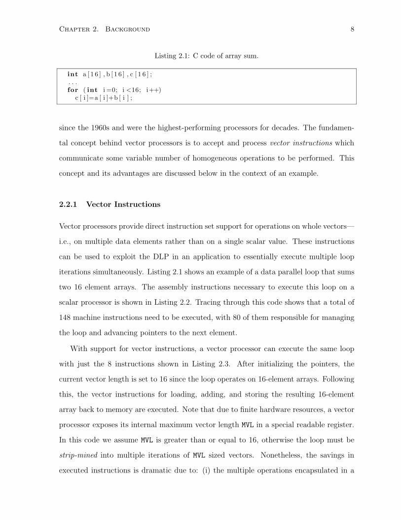
Listing 2.1: C code of array sum.
int a [ 1 6 ] , b [ 1 6 ] , c [ 1 6 ] ;. . .for ( int i =0; i <16; i++)
c [ i ]=a [ i ]+b [ i ] ;
since the 1960s and were the highest-performing processors for decades. The fundamen-
tal concept behind vector processors is to accept and process vector instructions which
communicate some variable number of homogeneous operations to be performed. This
concept and its advantages are discussed below in the context of an example.
2.2.1 Vector Instructions
Vector processors provide direct instruction set support for operations on whole vectors—
i.e., on multiple data elements rather than on a single scalar value. These instructions
can be used to exploit the DLP in an application to essentially execute multiple loop
iterations simultaneously. Listing 2.1 shows an example of a data parallel loop that sums
two 16 element arrays. The assembly instructions necessary to execute this loop on a
scalar processor is shown in Listing 2.2. Tracing through this code shows that a total of
148 machine instructions need to be executed, with 80 of them responsible for managing
the loop and advancing pointers to the next element.
With support for vector instructions, a vector processor can execute the same loop
with just the 8 instructions shown in Listing 2.3. After initializing the pointers, the
current vector length is set to 16 since the loop operates on 16-element arrays. Following
this, the vector instructions for loading, adding, and storing the resulting 16-element
array back to memory are executed. Note that due to finite hardware resources, a vector
processor exposes its internal maximum vector length MVL in a special readable register.
In this code we assume MVL is greater than or equal to 16, otherwise the loop must be
strip-mined into multiple iterations of MVL sized vectors. Nonetheless, the savings in
executed instructions is dramatic due to: (i) the multiple operations encapsulated in a

Chapter 2. Background 9
Listing 2.2: Pseudo-MIPS assembly of array sum. Destination registers are on the left.
move r1 , amove r2 , bmove r3 , cmove r7 , 0
loop add :load .w r4 , ( r1 )load .w r5 , ( r2 )add r6 , r4 , r5s t o r .w r6 , ( r3 )add r7 , r7 , 1 # Loop overheadadd r1 , r1 , r7 # Advance po in t e radd r2 , r2 , r7 # Advance po in t e radd r3 , r3 , r7 # Advance po in t e rb l t r7 , 1 6 , loop add # Loop overhead
Listing 2.3: Vectorized assembly of array sum. For simplicity it is assumed the maximum vectorlength is greater than or equal to 16.
move vbase1 , amove vbase2 , bmove vbase3 , cmove vl , 16 #Set vec tor l ength to 16vload .w vr4 , ( vbase1 )vload .w vr5 , ( vbase2 )vadd vr6 , vr4 , vr5vs to r .w vr6 , ( vbase3 )
single vector instruction; and (ii) the savings in loop overheads and pointer advancing.
Listing 2.3 shows the use of one possible vector instruction set. Many different vector
instruction sets have been extensively researched, including in modern processors [24].
Simultaneous research into the architectures that supports these vector instructions was
also thoroughly performed and is described next.
2.2.2 Vector Architecture
The vector architecture is responsible for accepting a stream of variable-lengthed vector
instructions and completing their associated operations as quickly as possible. We now
describe several architectural modifications that can be used to achieve this; a more
comprehensive summary can be found in [28].

Chapter 2. Background 10
time
time
time
space
space
vload
a) Base Vector Processor
vmul
vadd
vload
vadd
vmul
space
vload
vadd
vmul
c) Base Vector Processor with Chaining
b) Base Vector Processor with Lanes Doubled
Figure 2.1: Comparing vector execution of doubling lanes (b) and chaining (c) against a basevector processor (a). The area of the boxes represents the amount of work for each instruction.The base vector processor in (a) waits for each vector instruction to complete before executingthe next. In (b), doubling the number of lanes allows more of the work to be computed spatiallyon the additional lanes, this makes the instructions twice as tall in space and half as long intime. Chaining allows the work to be overlapped with the work of other instructions as seenin (c). The execution is staggered so that at any point in time each instruction is executing ondifferent element groups.
2.2.3 Vector Lanes
The most important architectural feature of a vector processor is the number of vector
datapaths or vector lanes. A single lane can operate on a single element of the vector at a
time in a pipelined fashion; with more vector lanes a vector processor can perform more
of the element operations in parallel hence increasing performance. For example, the
vadd instruction in Listing 2.3 encodes 16 additions to be performed across 16 elements.
A vector processor with 8 lanes can then execute 8 element operations at a time—we
refer to this group of elements as an element group. After the first element group with

Chapter 2. Background 11
indices 0-7 is processed, the next element group with indices 8-15 is processed and the
vadd instruction completes in two cycles.
Figure 2.1 shows a visual depiction of the effect of doubling lanes on vector instruction
execution. Compared to (a), doubling the number of lanes in (b) results in twice as much
spatial execution of the vector instructions, resulting in half as much execution time.
The number of lanes is a powerful parameter for trading silicon area (used for spatial
execution on the vector lanes) and performance (the time needed to complete the vector
instruction). Note that the number of lanes is always a power of two, otherwise accessing
an arbitrary element requires division and modulo operations to be performed.
2.2.4 Vector Chaining
Vector chaining provides another axis of scaling performance in addition to increasing
the number of lanes. Chaining allows multiple vector instructions to be executed simul-
taneously; the concept was first presented in the Cray-1 [56]. Using Listing 2.3 as an
example, the first element group of the vadd instruction does not need to wait for the
vload instruction preceding it to complete in its entirety. Rather, after the vload has
loaded the first element group into vr5, the vadd can execute its first element group since
its data is ready. Similarly the first element group for the stor can be stored as soon as
the vadd completes that element group. With this concept the throughput of the vector
processor can scale beyond the available number of lanes.
Figure 2.1 c) shows the effect of chaining compared to part a) of the same figure.
After an initial set of element groups have been processed, the next instruction can
execute alongside the previous. A continuous supply of vector instructions can lead to a
steady-state of multiple vector instructions in flight. However successful vector chaining
requires (i) available functional units, (ii) read/write access to multiple vector element
groups, and (iii) vector lengths long enough to access multiple element groups. The
first is achieved by replicating functional units, specifically the arithmetic and logic unit
(ALU). The second can be achieved by implementing many read/write ports to the vector

Chapter 2. Background 12
register file or many register banks each with their own read/write ports. Historically
vector supercomputers used the latter approach, while research in more modern single-
chip implementations of vector architectures have resorted to the former [6] as discussed
below. Finally the third requires applications with enough DLP to use vector lengths
longer than the number of lanes.
2.2.5 The T0 Vector Processor
While traditional vector supercomputers spanned multiple processor and memory chips,
Asanovic et. al. proposed harnessing advances in CMOS technologies to implement vec-
tor processors on a single chip with the aim of including them as add-ons to existing
scalar microprocessors [6, 7]. The 8-lane T0 vector processor was implemented with up
to 3-way chaining for a peak of 24 operations per cycle while issuing only one vector
instruction per cycle. A key contribution was in the reduction of the large delays histori-
cally associated with starting and completing a vector instruction. These delays require a
high-degree of data parallelism to be amortized, but with the shorter electrical delays of
a single-chip design, the delays were greatly reduced enabling new application classes to
exploit vector architectures. The T0 also first realized the area efficiency gains of using a
many-ported vector register file to support chaining rather than a many-banked register
file. Finally, while caches were not typically used in traditional vector supercomputers,
they are further motivated in the T0 which connects to DRAM instead of SRAM.
2.2.6 The VIRAM Vector Processor
The IRAM project [1] investigated placing memory and microprocessors on the same chip,
which lead to the design of a processor architecture that can best utilize the resulting high-
bandwidth low-latency access to memory. The group selected a vector processor based on
the T0, but optimized it for this memory system and for the embedded application domain
creating VIRAM [32, 33, 34, 35, 60]. The VIRAM vector processor was shown to provide
faster performance across several EEMBC industry-standard benchmarks compared to
Chapter 2. Background 13
superscalar and out-of-order processors while consuming less energy. The vector unit is
attached as a coprocessor to a scalar MIPS processor with both connected to the on-chip
DRAM. The complete system is manufactured in a 180nm CMOS process. The VIRAM
vector processor has 4 lanes each 64-bits wide but can be reconfigured into as many as
16 16-bit vector lanes. The architecture is massively pipelined with 15 stages in each
vector lane to tolerate the worst case on-chip memory latency. With this pipelining and
the low-latency on-chip DRAM, no cache is used in VIRAM. The soft vector processor
implemented in this thesis is based on the VIRAM instruction set which is described in
more detail below.
2.2.6.1 VIRAM Instruction Set
VIRAM supports a full range of integer and floating-point vector operations including
absolute value, and min/max instructions. Fixed-point operations are directly supported
by the instruction set as well, providing automatic scaling and saturation hardware.
VIRAM also supports predication, meaning each element operation in a vector instruction
has a corresponding flag indicating whether the operation is to be performed or not. This
allows loops with if/else constructs to be vectorized. Finally VIRAM has memory
instructions for describing consecutive, strided, and indexed memory access patterns.
The latter can be used to perform scatter/gather operations albeit with significantly less
performance than consecutive accesses.
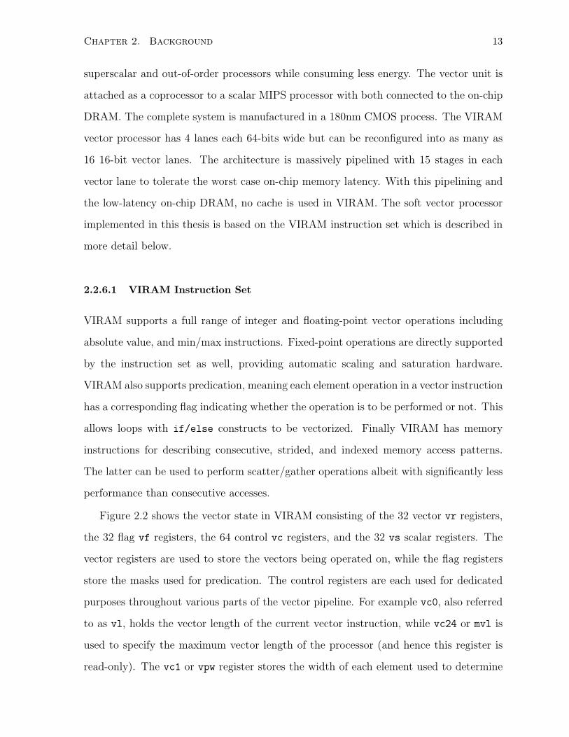
Figure 2.2 shows the vector state in VIRAM consisting of the 32 vector vr registers,
the 32 flag vf registers, the 64 control vc registers, and the 32 vs scalar registers. The
vector registers are used to store the vectors being operated on, while the flag registers
store the masks used for predication. The control registers are each used for dedicated
purposes throughout various parts of the vector pipeline. For example vc0, also referred
to as vl, holds the vector length of the current vector instruction, while vc24 or mvl is
used to specify the maximum vector length of the processor (and hence this register is
read-only). The vc1 or vpw register stores the width of each element used to determine
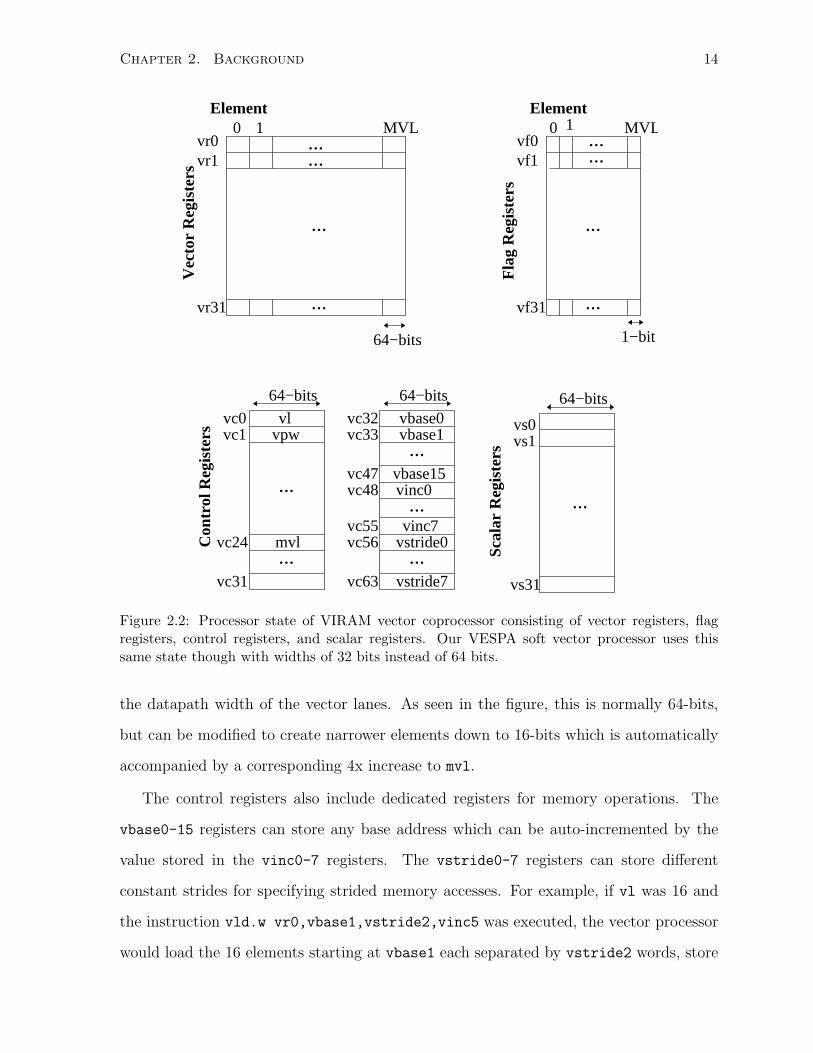
Chapter 2. Background 14
vc56 vstride0vc55 vinc7
...
vs0vs1
vs31
64−bits
Scal
ar R
egis
ters
vr0vr1
vr31
MVL10Element
Vec
tor
Reg
iste
rs
64−bits
...
...
...
...
vf0vf1
vf31
Element
Fla
g R
egis
ters
0 1
...
...
...
...MVL
1−bit
Con
trol
Reg
iste
rs
64−bits
vc31
vc1vc0 vl
...
...mvlvc24
64−bits
vc63
...
vc32vc33
vbase0vbase1
vstride7
...
...
vc48 vinc0vc47 vbase15
vpw
Figure 2.2: Processor state of VIRAM vector coprocessor consisting of vector registers, flagregisters, control registers, and scalar registers. Our VESPA soft vector processor uses thissame state though with widths of 32 bits instead of 64 bits.
the datapath width of the vector lanes. As seen in the figure, this is normally 64-bits,
but can be modified to create narrower elements down to 16-bits which is automatically
accompanied by a corresponding 4x increase to mvl.
The control registers also include dedicated registers for memory operations. The
vbase0-15 registers can store any base address which can be auto-incremented by the
value stored in the vinc0-7 registers. The vstride0-7 registers can store different
constant strides for specifying strided memory accesses. For example, if vl was 16 and
the instruction vld.w vr0,vbase1,vstride2,vinc5 was executed, the vector processor
would load the 16 elements starting at vbase1 each separated by vstride2 words, store

Chapter 2. Background 15
them in vr0, and finally update vbase1 by adding vinc5 to it. More detailed information
can be found in the VIRAM instruction set manual [60]. Note the implementation of
VIRAM used in VESPA uses exactly the same vector state as in Figure 2.2 except that
it is 32-bits instead of 64-bits, and without supporting the width reconfiguration using
vpw.
2.2.7 SIMD Extensions
Modern microprocessors exploit data-level parallelism via SIMD (single-instruction, multiple-
data) support, including IBM’s Altivec, AMD’s 3DNow!, MIPS’s MDMX, and Intel’s
MMX/SSE/AVX. SIMD support is very similar to vector support except that it is typi-
cally limited to a fixed and small number of elements which is exposed to the application
programmer. In contrast, true vector processing abstracts from the software the actual
number of hardware vector lanes, instead providing a machine-readable MVL parameter
(discussed below) for limiting vector lengths. This is partly due to the longer vector
lengths typically used in vector processing which are permitted to exceed the amount
of hardware resources so that future vector architectures could add hardware resources
to exploit the DLP without software modification. In addition, vector processors are
typically equipped with a wider range of vector memory instructions that can explic-
itly describe different memory access patterns. These features make vector processing
appealing for current microprocessors instead of the SIMD extensions used to date [24].
2.3 Field-Programmable Gate Arrays (FPGAs)
Field-Programmable Gate Arrays are prefabricated programmable logic devices often
composed of lookup table based programmable logic blocks connected by a programmable
routing network. Using these elements an FPGA can implement any digital logic circuit
making them (originally) useful for implementing miscellaneous glue logic. As FPGAs
have grown in capacity they have become capable of implementing complete embedded

Chapter 2. Background 16
systems. To augment their area efficiency and speed for certain operations, FPGA ven-
dors have included dedicated circuits for better implementing certain operations that are
typical in an embedded system. These dedicated circuits presently include flip flops, ran-
dom access memory (RAM), multiply-accumulate logic, and microprocessor cores [36].
We describe these in more detail below since they are used extensively in soft processors,
or in the case of the microprocessor cores, as an alternative to soft processors.
2.3.1 Block RAMs
The block RAMs in FPGAs provide efficient large storage structures which would oth-
erwise require large amounts of lookup tables and flip flops to implement. While the
capacity of a given block RAM is fixed, multiple block RAMs can be connected to form
larger capacity RAM storage. Additional flexibility is available in the width and depth
of the block RAMs allowing them to be configured as deep and narrow 1-bit memories,
or shallow and wide 32-bit memories. A key limitation of block RAMs is they have only
two access ports allowing just two simultaneous reads or writes to occur. This limitation
inhibits soft processor architectures which require many-ported register files to sustain
multiple instructions in flight. As a result most soft processor research has been on
single-issue pipelines or multiprocessors.
2.3.2 Multiply-Accumulate blocks
The multiply-accumulate blocks, referred to also as DSP blocks, have dedicated circuitry
for performing multiply and accumulate operations. The smallest such blocks are 9 or
18 bits wide and can be combined to perform multiply-accumulate for larger inputs. In
this work we use the multiply-accumulate blocks to efficiently implement the multiplier
functional units in a processor, which we also use to perform shift operations since barrel
shifters are inefficient when built out of lookup tables.
Chapter 2. Background 17
2.3.3 Microprocessor Cores
Some FPGAs include one or two microprocessor cores implemented directly in silicon
with the FPGA programmable fabric surrounding it [4, 68]. These hard processors pro-
vide superior performance relative to a soft processor but also have many disadvantages:
(i) the number of hard processors on an FPGA may be insufficient or too many resulting
in wasted silicon; (ii) the architecture is fixed making it difficult to satisfy all application
domains; (iii) the cost of the FPGA is increased since vendors must design, build, and/or
license a processor core; and (iv) the FPGA is specialized often producing multiple fami-
lies of devices with/without processor cores which further increases design and inventory
costs. As a result soft processors have seen significant uptake by both vendors and FPGA
users, motivating research into improving soft processors.
2.4 FPGA Design
The typical FPGA design flow begins with an HDL language such as Verilog or VHDL
which describes the desired circuit. FPGA vendors provide computer-aided design (CAD)
tools for parsing this description and efficiently mapping the circuit onto the FPGA fabric.
This design process is far more difficult than the software-based flows of microprocessors.
An FPGA designer must specify the cycle-to-cycle behaviour of each component of the
system, and the interaction between these components creates many opportunities for
errors. Unlike the single-stepping debug infrastructure in a microprocessor, debugging a
hardware design is very difficult. A logic analyzer can be used to capture a snapshot of
a few signals at some event, but finding the erroneous event among its many symptoms
can involve weeks of effort. In addition, an FPGA designer must respect the timing
constraints of the system. Doing so requires pipelining, retiming, and other optimizations
which can create more state and hence increased opportunities for errors. Overall, the
biggest bottleneck of the FPGA design process is the design and verification of the desired
system. Unlike an ASIC, fabrication is performed in minutes to days depending on the
Chapter 2. Background 18
circuit size and the compilation time of the FPGA CAD tools.
2.4.1 Behavioural Synthesis
Many efforts have been made to simplify the FPGA design flow. One option adopted by
the FPGA vendors is to use processors (soft or hard) to implement less critical compo-
nents and system control tasks—where errors can be very difficult to find if implemented
in a hardware finite state machine (FSM). But another option which has been extensively
researched in both FPGAs and ASICs is to automatically derive hardware implementa-
tions from a C-like sequential program. This is referred to as behavioural synthesis and
its goal is aligned with our own goal of simplifying FPGA-design by using sequential
programming for soft processors instead. Some examples of behavioural synthesis tools
and languages include Handel-C [59], Catapult-C [43], Impulse C [52], and SystemC [51].
Altera has their own behavioural synthesis tool called C2H [40] which can convert C
functions into hardware accelerators attached to a Nios II soft processor. Previous work
has shown that soft vector processors can scale significantly better than C2H-generated
accelerators even when manual code-restructuring is performed to aid C2H [75]. The
state-of-the-art behavioural synthesis results in overheads due to the intractable nature
of the problem including the pointer aliasing problem. These complexities have limited
the quality of results available from behavioural synthesis tools.
We believe that customized processors will continue to be useful until and even after
high-quality behavioural synthesis tools exist because of the following advantages.
1. Fluid Design Methodology – Processors have well-defined intermediate steps
throughout the design flow. Each of these steps are taught to engineers at the
undergraduate level providing them with the knowledge to manually optimize the
algorithm, compiler, assembler output, and processor architecture. Behavioural
synthesis tools aim to reap the efficiency gains from not having a fixed architecture
structure or instruction set. As a result it is difficult for designers to manually
navigate the vastly different hardware implementations possible.
Chapter 2. Background 19
2. Libraries – For a processor, compiled output can be packaged and shared very
easily between software designers. This same idea has failed to gain traction in
hardware design because of differing speed/area constraints and non-standardized
interfaces. In contrast, software is decoupled from the hardware implementation
allowing it to be designed primarily for speed. Moreover, libraries can preserve
manual optimization of the compiled software.
3. Debug Support – Processors provide single-step debug capability. While this
can be emulated to some degree by hardware simulators, the parallel nature of
hardware can make it confusing. In addition, hardware simulators can not precisely
model the behaviour of the hardware itself because of external stimuli and hardware
imperfections. Inevitably this means some bugs will manifest only in the hardware
implementation where they are difficult to find and fix.
4. Intractable Complexities – The complexities in deriving a high-quality hardware
implementation of a system has made it a holy grail for many decades. Until high-
quality behavioural synthesis exists, designers can instead utilize the customization
opportunities in microprocessor systems. The knowledge gained through this re-
search can also be used for improving behavioural synthesis tools.
5. ANSI C Support – Overcoming the complexities in behavioural synthesis most
often leads to limited support for the full ANSI C standard or radically different
programming models. Some examples of these are summarized below, however
the willingness of FPGA designers to adopt new C variants or programming models
casts doubt on the future adoption of behavioural synthesis. In contrast a processor
can easily support full ANSI C which provides a familiar programming interface.
One of the largest hurdles to supporting full ANSI C in behavioural synthesis is the
global memory model used in high-level programming languages. While arithmetic oper-
ations can be literally converted to hardware circuits, a literal conversion of this memory
model would result in many processing elements being sequenced to preserve memory
Chapter 2. Background 20
consistency but at the same time competing over the single memory. The CHiMPS [54]
project aims to support traditional memory models by providing caches for many pro-
cessing elements. Compiler analysis determines regions of memory safe for caching by
analyzing dependencies in scientific computing applications which rarely have complex
memory aliasing. Additionally, traditional memory models can be preserved with multi-
threaded and/or multi-processor systems but programming these systems requires facing
the difficult parallel programming problem. The implementation of these systems onto
FPGAs leads to soft processor research which is summarized in Section 2.5.3 and Sec-
tion 2.5.4.
Most behavioural synthesis compilers modify or restrict the memory model to facili-
tate better quality hardware implementations. The SA-C [17] compiler prohibits the use
of pointers and recursion and forces all variables to be single-assignment. While these
restrictions impose difficulties on the programmer, the resulting application code can be
more easily converted to hardware. The streaming programming paradigm has also been
researched as a means of programming FPGAs. For example the Streams-C [25] language
allows a programmer to express their computation in a consume-compute-produce model.
Data and task level parallelism can be extracted and used to build parallel hardware for
faster execution. Similar work was done using the Brook stream language [53] and also
using regular C file I/O streams for the PACT behavioural synthesis tool [48] [30].
2.4.2 Extensible Processors
Behavioural synthesis aims to convert whole programs into hardware, but other ap-
proaches are premised on the common characteristic that a small computation is largely
responsible for overall performance. The Warp [42] processing project derives on-the-
fly hardware accelerators for a simplified FPGA fabric. This allows an application to
be programmed in C and executed on a generic microprocessor which will automati-
cally accelerate critical computations. The eMIPS [44] project converts blocks of binary
MIPS instructions to hardware that can be dynamically configured onto an FPGA. The
Chapter 2. Background 21
instructions are then replaced with an invocation of the hardware accelerator. These
dynamically extensible processors can be used to accelerate software and avoid custom
hardware design similar to our own goals. However they are accompanied with significant
overhead in synthesizing and configuring hardware accelerators and are hence critically
dependent on correctly identifying computation to accelerate. This decision depends on
how amenable the computation is to hardware acceleration and also depends on its overall
contribution to system performance. As the system is improved and computation is more
balanced across different kernels, it becomes increasingly difficult to select a computation
which can amortize the dynamic configuration overheads.
2.5 Soft Processors and Related Work
Soft processors are processors designed for a reprogrammable fabric such as an FPGA.
The two key attributes of soft processors are (i) the ease with which they can be cus-
tomized and subsequently implemented in hardware, and (ii) that they are designed to
target the fixed resources available on a reprogrammable fabric. This distinguishes soft
processors from hard processors which are extremely difficult to customize due to the high
cost and long design and fabrication times of full-custom VLSI design. Also, soft proces-
sors are distinct from parameterized processor cores which are pre-designed synthesizable
RTL implementations not necessarily targeting efficient FPGA implementation.
The Actel Cortex-M1 [2], Altera Nios II [5], Lattice Micro32 [39], and Xilinx Microb-
laze [67] are widely used soft processors with scalar in-order single-issue architectures that
are either unpipelined or have between 3 and 5 pipeline stages. While this is sufficient
for system coordination tasks and least-critical computations, significant performance
improvements are necessary for soft processors to replace the hardware designs of more
important system components. Research in this direction is recent and ongoing, and
summarized below.
Chapter 2. Background 22
2.5.1 Soft Single-Issue In-Order Pipelines
The SPREE (Soft Processor Rapid Exploration Environment) system was developed to
explore the architectural space of current soft processors in our previous research [69,
70, 71]. SPREE can automatically generate a Verilog hardware implementation of a pro-
cessor from a higher-level description of the datapath and instruction set. The tool was
used to explore the implementation and latencies of functional units as well as the depth
and organization of pipeline stages creating a thorough space of soft processor design
points that were competitive with the slower and mid-range Altera Nios II commercial
soft processors. We found diminishing returns with deeper pipelining which required
more advanced architectural features to avoid pipeline stalls. While this work succeeded
in exploring the space and finding processor configurations superior to a mid-speed com-
mercial soft processor, it failed to extend the space, specifically with faster soft processors.
In this thesis, we continue to use SPREE by choosing the best overall generated design
and manually adding vector extensions to the architecture and compiler infrastructure.
Numerous other works created parameterized scalar soft processors aimed at cus-
tomization. The LEON [23] is a parameterized VHDL description of a SPARC processor
targetted for both FPGAs and ASICS with several customization options including cache
configuration and functional unit support. LEON is heavily focussed on system-level fea-
tures fully supporting exceptions, virtual memory, and multiprocessors. No scalable per-
formance options exist other than multiprocessing which requires parallelized code. Sim-
ilarly the XiRisc [41] is a parameterized core written in VHDL supporting 2-way VLIW,
16/32-bit datapaths, and optional shifter, multiplier, divider, and multiply-accumulate
units. While these options provide some performance improvements it cannot scale to
compete with manual hardware design. Other VLIW processors are discussed below.
2.5.2 Soft Multi-Issue Pipelines
The idea of using VLIW (Very Long Instruction Word) processors in which batches of
independent instructions are submitted to the processor pipeline has been explored as
Chapter 2. Background 23
a way of increasing soft processor performance without the complexities of hardware
scheduling. Saghir et. al. implemented a soft VLIW processor using a register file with
2 banks replicated 4 times to achieve the 4 read ports and 2 write ports necessary to
sustain two instructions per cycle [57]. For an fir benchmark this configuration achieved
up to 2.55x speedup with 3 data write ports and 2 address write ports over 1 data write
port and 1 address write port. Bank conflicts and limits to instruction level parallelism
limit the performance scaling possible on soft VLIW processors, moreover the increasing
register file replication necessary would quickly become overwhelming. Jones et. al.
implemented a 4-way VLIW processor by implementing the register file in logic instead
of block RAMs [31]. This 4-way parallelism averaged only 29% speedup over single-issue,
suggesting that the technique cannot easily scale performance.
A superscalar processor can issue multiple instructions concurrently, but unlike VLIW
processors, a superscalar automatically identifies and schedules independent instructions
in hardware. While this approach is popular in hard processors, there is presently no
soft superscalar architectures in existence likely due to their complexity. Also, the large
associative circuit structures and many-ported register file required to build a superscalar
are not efficiently implementable in FPGAs. Carli designed an out-of-order single-issue
soft MIPS processor that implements Tomasulo’s algorithm and discusses the infeasibility
of superscalar issue with respect to his architecture [12]. The soft MIPS was found to be
up to twice as big as a Xilinx Microblaze and between 3x and 12x slower.
2.5.3 Soft Multi-Threaded Pipelines
A potentially promising method of scaling soft processor performance is to leverage multi-
ple threads. Research into exploiting multiple threads in soft processors will only become
more fruitful as advancements in parallel programming are made in the microprocessor in-
dustry. Nonetheless, auto-vectorization is a significantly simpler problem which exploits
predominantly fine-grain data parallelism and is hence supported in many compilers in-
cluding GCC.
Chapter 2. Background 24
The advanced architectural features needed to keep a pipeline fully utilized can be
avoided by instead having multiple independent instruction streams (threads), which
can also be used to hide system latencies. Fort et. al. showed that a multithreaded
soft processor can save significant area while hiding memory latencies and performing as
fast as a multiprocessor system when both use an uncached latent memory system [21].
Labrecque et. al. showed that multithreading can save logic by eliminating branch
handling and data dependency hardware [37]. They also showed that with an off-chip
DRAM memory system the amount of hardware threads, cache configuration, cache
topology, and number of cores can be varied to achieve maximum throughput from the
memory system [38]. Moussali [47] built a multi-threaded version of the Xilinx Microblaze
and showed that 1.1x to 5x performance can be gained by hiding the latency caused by
custom instructions and custom computation blocks.
The CUSTARD [15, 16] customizable threaded soft processor is an FPGA implemen-
tation of a parameterizable core supporting the following options: different number of
hardware threads and types, custom instructions, branch delay slot, load delay slot, for-
warding, and register file size. The primary purpose of the design was to be used with
a tool for automatic custom instruction generation. However its uses as a parameterized
soft processor is more applicable to our own work. While the available architectural axes
are interesting the results show some overheads in the processor design: clock speed var-
ied only between 30 and 50 MHz on the XC2V2000 FPGA (on which the Microblaze soft
processor is clocked at 100 MHz), and overall performance is 6-61% worse than Microb-
laze. Also the single-threaded base processor consumed 1800 slices while the commercial
Microblaze typically consumes less than 1000 slices on the same device. Nonetheless
4-way multi-threading can be added for only 28% more area but was shown to gain only
10% in performance.
Chapter 2. Background 25
2.5.4 Soft Multiprocessors
Unnikrishnan et. al. created a tool for automating the parallelization of streaming code
and making application-specific customizations to the targetted soft multiprocessor sys-
tem [62]. The individual cores could be customized to their software eliminating unused
hardware using our SPREE framework and achieving significant area savings. With 16
processors up to 5x increased performance can be achieved using this tool. Similarly,
Plavec et. al. [53] developed a tool to generate a streaming architecture comprised of
multiple processor cores from a streaming program. The Altera C2H behavioural syn-
thesis tool is leveraged to convert processor nodes to custom hardware achieving further
speed improvements. The generated and optimized streaming architecture can perform
up to 8.9x faster than execution on a single soft processor, as well as 4.3x faster than using
C2H on the entire benchmark kernel. Similar to our own work, these stream-based design
flows can provide scalable soft processor performance if streaming languages are adopted
by embedded system designers. An auto-vectorizing compiler or vectorized library could
provide this scalability with minimal disruption to current design flows.
Ravindran et. al. built a soft multiprocessor system dedicated to IPv4 packet for-
warding [55]. The 14-processor system was able to achieve a throughput of 1.8Gbps,
which when normalized to area is 2.6x slower than the Intel IXP-2800 network proces-
sor. This case study show the potential of FPGA-based multiprocessors to compete
with highly optimized and specialized commercial hard multiprocessors. Rigorous man-
ual parallelization was required and the multiprocessor topology was customized, but
customizing each individual core was not performed as the authors used standard Xilinx
Microblaze cores. More aggressive customization would require extensive software and
hardware labour, but can perhaps be automated in the future.
2.5.5 Soft Vector Processors
Yu et. al. [75] first demonstrated the potential for vector processing as a simple-to-use
and scalable accelerator for soft processors. In particular, through performance mod-

Chapter 2. Background 26
elling the authors show that (i) a vector processor can potentially accelerate data paral-
lel benchmarks with performance scaling better than Altera’s C2H behavioural synthesis
tool (even after manual code restructuring to aid C2H), and (ii) how FPGA architectural
features can be exploited to provide efficient support for some vector operations. For
example, the multiply-accumulate blocks internally sum multiple partial products from
narrow multiplier circuits to implement wider multiplication operations. This same ac-
cumulator circuitry is used by Yu to efficiently perform vector reductions which sum all
vector elements and produce a single scalar value. Also the block RAMs can be used as
small lane-local memories for efficiently implementing table lookups and scatter/gather
operations.
The work of Yu et. al. was done in parallel with our own development of VESPA and
its infrastructure, but it left many avenues unexplored. Its memory system consisted of
only the fast on-chip block RAMs—latent memory systems were never explored. Without
this and without real execution of benchmarks, the scalability of soft vector processors
remains unproven. Also few customization opportunities in soft vector processors were
examined beyond the number of lanes and the maximum vector length: the width of
the lanes, multiplier, and memory were parameterized and were individually set for each
benchmark. Finally more sophisticated vector pipelines features such as vector chain-
ing were never considered. Beyond the work of Yu, in this thesis, we offer a full and
verified hardware implementation of a soft vector processor called VESPA, connected
to off-chip memory, with GNU assembler vector support, and evaluation on vectorized
industry-standard benchmarks. This thesis more thoroughly explores the scalability,
customizability, and architecture of soft vector processors. In addition, we explore the
design space of VESPA configurations and show how competitive it can be versus manual
hardware design in Chapter 8.
Chapter 3
Experimental Framework
Our goal of improving soft processors to be more competitive with hardware requires a
measurement infrastructure for accurately and thoroughly evaluating enhancements to
soft processors. In this chapter we describe the infrastructure used for executing, verify-
ing, and evaluating soft processors. Specifically, we describe the benchmarks, compiler,
CAD software, hardware platforms, measurement methodology, measurement error, and
verification process.
3.1 Overview
We employ a real and complete measurement infrastructure which implements soft pro-
cessors in hardware executing benchmarks on real FPGA devices. An overview of the
infrastructure is illustrated in Figure 3.1. Benchmark software programs are compiled
with standard compilers and simulated at the instruction-level to verify their correctness.
Architectural ideas are augmented into a complete Verilog design of a soft processor and
simulated at the register transfer level (RTL) using an RTL simulator. Once the correct-
ness of the architecture is verified, the design is synthesized using FPGA computer-aided
design (CAD) software which emit hardware characteristics such as the area and clock
frequency of the design. The soft processor is then configured onto a real FPGA and
executes each benchmark from off-chip DRAM—at the end of each execution the to-
27
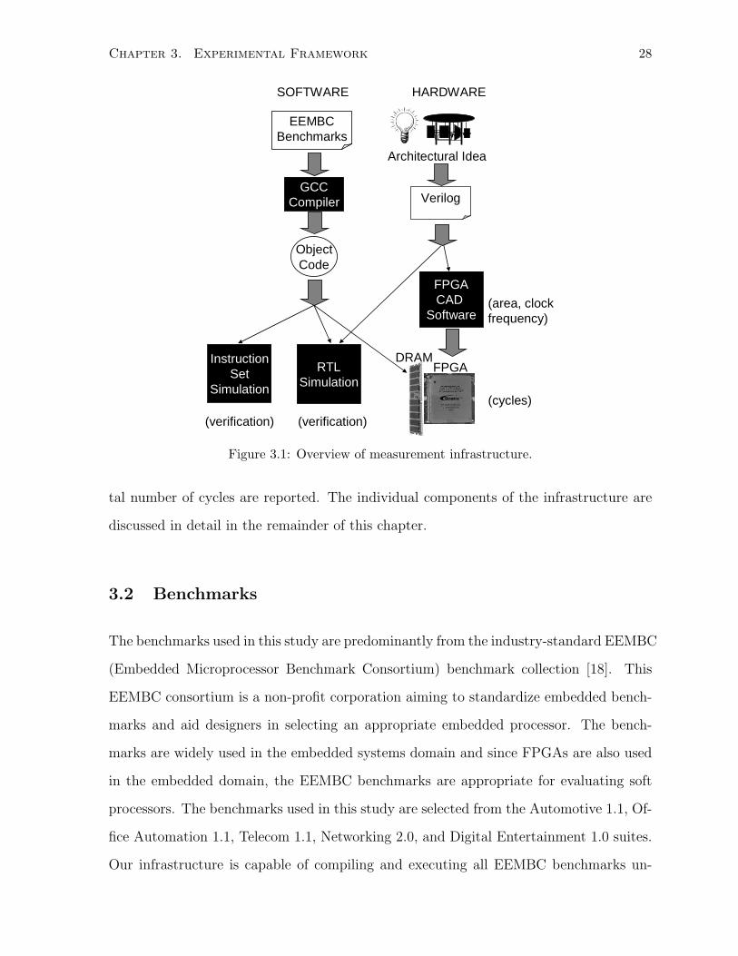
Chapter 3. Experimental Framework 28
Verilog
ObjectCode
InstructionSet
Simulation
EEMBCBenchmarks
RTLSimulation
SOFTWARE HARDWARE
Architectural Idea
FPGACAD
Software
(cycles)
(area, clockfrequency)
GCCCompiler
(verification) (verification)
FPGADRAM
Figure 3.1: Overview of measurement infrastructure.
tal number of cycles are reported. The individual components of the infrastructure are
discussed in detail in the remainder of this chapter.
3.2 Benchmarks
The benchmarks used in this study are predominantly from the industry-standard EEMBC
(Embedded Microprocessor Benchmark Consortium) benchmark collection [18]. This
EEMBC consortium is a non-profit corporation aiming to standardize embedded bench-
marks and aid designers in selecting an appropriate embedded processor. The bench-
marks are widely used in the embedded systems domain and since FPGAs are also used
in the embedded domain, the EEMBC benchmarks are appropriate for evaluating soft
processors. The benchmarks used in this study are selected from the Automotive 1.1, Of-
fice Automation 1.1, Telecom 1.1, Networking 2.0, and Digital Entertainment 1.0 suites.
Our infrastructure is capable of compiling and executing all EEMBC benchmarks un-
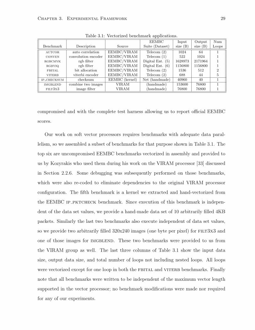
Chapter 3. Experimental Framework 29
Table 3.1: Vectorized benchmark applications.EEMBC Input Output Num
Benchmark Description Source Suite (Dataset) size (B) size (B) Loops
autcor auto correlation EEMBC/VIRAM Telecom (2) 1024 64 1conven convolution encoder EEMBC/VIRAM Telecom (1) 522 1024 1
rgbcmyk rgb filter EEMBC/VIRAM Digital Ent. (5) 1628973 2171964 1rgbyiq rgb filter EEMBC/VIRAM Digital Ent. (6) 1156800 1156800 1fbital bit allocation EEMBC/VIRAM Telecom (2) 1536 512 2viterb viterbi encoder EEMBC/VIRAM Telecom (2) 688 44 5
ip checksum checksum EEMBC (kernel) Net (handmade) 40960 40 1
imgblend combine two images VIRAM (handmade) 153600 76800 1filt3x3 image filter VIRAM (handmade) 76800 76800 1
compromised and with the complete test harness allowing us to report official EEMBC
scores.
Our work on soft vector processors requires benchmarks with adequate data paral-
lelism, so we assembled a subset of benchmarks for that purpose shown in Table 3.1. The
top six are uncompromised EEMBC benchmarks vectorized in assembly and provided to
us by Kozyrakis who used them during his work on the VIRAM processor [33] discussed
in Section 2.2.6. Some debugging was subsequently performed on those benchmarks,
which were also re-coded to eliminate dependencies to the original VIRAM processor
configuration. The fifth benchmark is a kernel we extracted and hand-vectorized from
the EEMBC ip pktcheck benchmark. Since execution of this benchmark is indepen-
dent of the data set values, we provide a hand-made data set of 10 arbitrarily filled 4KB
packets. Similarly the last two benchmarks also execute independent of data set values,
so we provide two arbitrarily filled 320x240 images (one byte per pixel) for filt3x3 and
one of those images for imgblend. These two benchmarks were provided to us from
the VIRAM group as well. The last three columns of Table 3.1 show the input data
size, output data size, and total number of loops not including nested loops. All loops
were vectorized except for one loop in both the fbital and viterb benchmarks. Finally
note that all benchmarks were written to be independent of the maximum vector length
supported in the vector processor; no benchmark modifications were made nor required
for any of our experiments.

Chapter 3. Experimental Framework 30
3.3 Software Compilation Framework
Benchmarks are compiled using GNU GCC 4.2.0 ported to MIPS to match the MIPS-
based SPREE scalar processors used throughout this work. Benchmarks are compiled
with -O3 optimization level. GCC has internal support for auto-vectorization potentially
enabling soft vector processors to be employed without manual software changes. How-
ever, experiments with this feature showed that it failed to vectorize all key loops in the
EEMBC benchmarks above. Using GCC 4.3.3 only the autcor benchmark was success-
fully vectorized. We expect this technology to better incorporated in GCC in the future.
Commercial compilers such as the Intel C Compiler likely have better auto-vectorization
support but is closed-source making it impossible to port to our VIRAM vector instruc-
tion set. Instead of relying on auto-vectorization, we ported the GNU assembler found
in binutils version 2.1.6 to support our VIRAM vector instruction set, allowing us to
hand-vectorize loops in assembly, compile it into a regular application binary, as well as
disassemble the compiled result.
3.4 FPGA CAD Software
A key value of performing FPGA-based processor research directly on an FPGA is the
ability to attain high quality measurements of the area consumed and the clock frequency
achieved—these are provided by the FPGA CAD software. In this research we use Altera
Quartus II version 8.1. There are many settings and optimizations that one can enable
within the software, creating a wide range of synthesis results. In our work the settings
used are those suggested in previous research [69] which identified them as a good area,
clock frequency, and runtime tradeoff. First, we request that the CAD tool attempt to
attain a 200 MHz clock frequency despite the fact that our soft processors are incapable
of reaching such a high clock frequency. By doing this the CAD software thoroughly
optimizes the clock frequency of the design. Second, we enable the optimizations for
register retiming and register duplication as suggested. All other settings are left at their
Chapter 3. Experimental Framework 31
default values.
3.4.1 Measuring Area
Area is comprised mostly of the FPGA programmable logic blocks described in Sec-
tion 2.3. Throughout this work two generations of FPGAs are used: the Stratix I
and Stratix III on which the programmable logic blocks are respectively referred to as
Logic Elements (LEs) and Adaptive Logic Modules (ALMs). Soft processors also make
use of memory blocks and multiply-accumulate blocks in their designs creating a multi-
dimensional area measurement, which we reduce to a single scalar measurement of the
total silicon area used by all the occupied FPGA resources. The silicon areas of each
FPGA resource relative to a single programmable logic block including its routing was
provided to us from Altera [13] for the Stratix I and Stratix II. The relative silicon areas
are proprietary and hence cannot be released in this document. We used these numbers
for the Stratix I and extrapolated them for the Stratix III and measured the total silicon
area consumed. We report the areas for the Stratix I and Stratix III respectively in units
of equivalent LEs and equivalent ALMs.
3.4.2 Measuring Clock Frequency
The clock frequency of a synthesized design is reported by the timing analysis tool in
the FPGA CAD software. In addition to the settings described above, the actual device
targeted can affect these results because of differing architecture, circuit design, and IC
fabrication process used in creating the FPGA. Rather than targeting the FPGA devices
used in this work (which are slower mid-speed devices as described in the next section),
we instead measure clock frequency by targeting a Stratix III EP3SL340H1152C2 which
is a faster device than those on our hardware platforms. Doing this accurately reflects
the speeds achievable on state-of-the-art FPGAs rather than limiting our results to the
devices available to us.
Chapter 3. Experimental Framework 32
3.5 Hardware Platforms
All soft processors explored in this work are fully synthesized using the CAD flow de-
scribed above and implemented in hardware on an FPGA system. A hardware implemen-
tation is necessary to quickly benchmark a soft processor—an analysis of the execution
speeds of hardware over software simulation is presented in Section 3.8. Benchmarks
are executed in hardware and report the precise number of clock cycles required to
complete execution. The majority of this work was done on the University of Toronto
Transmogrifier-4 board, but prior to writing, we ported some of our work to the new
Altera DE3 board. We describe each of these hardware platforms below and specify in
our results which was used in the corresponding experiments.
3.5.1 Transmogrifier-4
The Transmogrifier-4 [19] is a multi-FPGA platform with four Altera Stratix 1S80F1508C6
devices on it (a high-end large-capacity FPGA device fabricated in 130nm technology).
This system was developed at the University of Toronto until completed in 2005 and was
intended for graphics and other compute-intensive streaming applications. It is equipped
with many peripherals such as video and Firewire connections, but the most important
non-FPGA component for our purposes is the two 1GB DIMMs of DDR-266 SDRAM
available for each of the four FPGAs. Only one Stratix I FPGA is used to host a soft
processor design and one of the connected DIMMs is used to store the instruction and
data for an application. The memory system is clocked at 133 MHz (266 MHz dual data
rate).
The TM4 was selected for our studies of soft processor design for a few reasons. First,
it provides a communication layer between user-designs on the FPGA(s) to a host Linux
computer simplifying the design of an I/O subsystem. This communication package is
referred to as the TM4 Ports Package. Second, it has a pre-verified memory controller
design available. And finally, it has an abundance of DDR SDRAM on it whereas the
Chapter 3. Experimental Framework 33
FPGA development kits at that time had only SRAM or only 16MB of DRAM. We
believe it is important to use DRAM technology since the desktop market will continue
to commoditize it making DRAM the cost-effective choice for embedded designs.
3.5.2 Terasic DE3
The Terasic DE3 boards were released in 2008 offering more up-to-date FPGA and DRAM
technologies. We use the Terasic DE3-340 board equipped with a single Stratix III
EP3SL340H1152C3 which is one of the largest state-of-the-art FPGAs available at the
time this work was performed. The Stratix III is fabricated in a 65nm CMOS technology
process making it two generations more advanced than the Stratix I FPGAs on the TM4.
We also use a 1GB DDR2-533 MHz memory device for the storage of instructions and
data in a program. The Altera DDR2 memory controller connects the soft processor to
the DDR2 DIMM and is clocked at the full-rate of 266 MHz.
3.5.3 Measuring Wall Clock Time
The implementation onto a real FPGA hardware platform enables accurate measurement
of not just the execution cycles (which traditionally was only modelled in the computer
architecture community) but also the wall clock time for executing a benchmark. Wall
clock time considers both cycle performance and clock frequency of a processor. Measur-
ing wall clock time is ideally performed by clocking the design at its highest clock rate,
measuring the number of clock cycles to execute a benchmark, and then multiplying the
number of cycles by the clock period. To avoid complications that arise from clocking
each design at a custom rate, we clock all designs at one clock frequency. On the TM4
this is 50 MHz and on the DE3 it is 100 MHz. Thus our calculation of wall clock time is
given by
WCT = Ncycles@50or100MHz/fcpu (3.1)
where fcpu is the maximum clock frequency of the soft processor and Ncycles@50or100MHz
Chapter 3. Experimental Framework 34
is the number of cycles to complete the benchmark when clocked at 50 or 100 MHz
depending on the platform. Typically the soft processor can be clocked higher than
these frequencies, meaning we are underclocking the soft processors.
3.6 Measurement Error
Errors in our measurement methodology exist due to simplifications made, randomness in
the CAD software, and physical effects in our realistic infrastructure. These errors affect
the area, cycles, clock frequency, and wall clock time measurements and are detailed
below.
1. Area: Area measurements are subject to two sources of errors: (i) the synthesis
algorithms which can produce significantly different hardware implementations from
minor perturbations to the Verilog source; and (ii) the approximation of the silicon
areas of each resource on the Stratix III which we derived from the Stratix II. The
first is difficult to mitigate, the second cannot be discussed to protect the intellectual
property rights of the vendor.
2. Cycles: The number of cycles reported at the end of benchmark execution is
precisely measured, but certain events can randomly occur during execution altering
the measurement with each run. A DRAM refresh command is one such example,
as is settling times between signals crossing clock domains. In general this affected
only the least significant digit of cycle measurements while benchmarks executed
between thousands and millions of cycles. The error is hence ignored.
3. Clock Frequency: Clock frequency measurements can vary significantly from the
non-determinism in modern CAD algorithms which produce different clock frequen-
cies depending on an integer seed selected by the user. To filter out the noise caused
by this non-determinism, we select 8 different seeds and average the clock frequency
across the 8 runs as suggested in [69]. This averaging minimizes the amount of mea-
surement error in our methodology.
Chapter 3. Experimental Framework 35
4. Wall Clock Time: As mentioned previously, measuring the maximum clock fre-
quency of a design and achieving a design that can operate correctly at that fre-
quency introduces additional complications. These complications are avoided by
underclocking all designs at the same clock frequency and using Equation 3.1 which
leads to time dilation effects between the processor and memory. Underclocking
a processor design means fewer processor cycles are needed to match the memory
latency. Scaling those cycles by a faster clock rate falsely accelerates the memory
latency as well. In Chapter 4 we show that cache misses are not a major contributor
to scalar soft processors, and in Chapter 6 we show that prefetching can minimize
their impact on performance so we ignore these effects.
3.7 Verification
All soft processors were fully tested in hardware using the built-in verification encoded
into each EEMBC benchmark. At the end of each benchmark a checksum is computed
across the output data and compared to a built-in gold-standard value to determine if ex-
ecution completed successfully. If the verification fails, it can be extraordinarily difficult
to uncover and fix bugs given that manual modifications were made to the benchmarks,
the assembler, the simulator, and the hardware design. As a result, developing a pow-
erful test and debug infrastructure with multiple abstraction levels is imperative for
in-hardware exploration of architectures.
3.7.1 Instruction Set Simulation
One useful abstraction is simulation at the instruction-level which is performed inde-
pendent of any architecture. Instruction set simulation can verify the correctness of the
benchmark and assembler hence ruling out bugs in these components. However without
a pre-verified VIRAM simulator available, considerable time was spent augmenting an
existing simulator with VIRAM extensions and simultaneously debugging it with the
Chapter 3. Experimental Framework 36
benchmarks and assembler.
Our simulator is based on the MINT [64] MIPS simulator which is pre-verified and
can successfully execute the scalar MIPS code in our benchmarks. MINT models only
the MIPS state and parses instructions in the binary and appropriately updates the
state. We augmented this simulator with support for the VIRAM vector instruction set
modelling all the vector state described in Section 2.2.6. In addition we parse and execute
the vector instructions by correspondingly modifying the vector state. Once verified, the
augmented MINT simulator was used to verify the benchmarks and compiler, analyze
the instruction streams of the benchmarks, and even model caches and other processor
components to predict their effectiveness. The most important use of the the simulator
however is to generate traces of all modifications to the vector state which is used to
compare against by the RTL simulation described below.
3.7.2 Register Transfer Level (RTL) Simulation
RTL simulation is performed using Modelsim SE version 6.3c which can simulate the
Verilog design in software (avoiding hardware timing problems such as crossing a clock
domain). The complete system is simulated including the processor, bus, and even DDR
controller. The behaviour of the TM4 DDR DIMM is modelled in Verilog using a hand-
made memory model, as is the TM4 communication package which is stimulated with
bus transactions that emulate the TM4-to-host transactions. The DE3 DDR2 memory
is modelled with the Altera generated memory model. With this level of simulation we
can capture logic errors throughout the complete hardware system. Similar to MINT,
the RTL simulation emits a complete trace of all modifications made to the vector state.
By comparing this trace to that from MINT, we can identify: (i) the instruction which
triggered the error; (ii) the incorrect value computed; and (iii) the exact time in the
waveform the error occurred. This trace-guided debug infrastructure is used extensively
before implementing a design in hardware.

Chapter 3. Experimental Framework 37
Table 3.2: Benchmark execution speeds.Platform Instructions/s Normalized Speedup
DE3 68970334 2383961MINT 76458 2643
Modelsim 29 1
3.7.3 In-Hardware Debugging
Despite the simulation at the instruction and RTL level, inevitably some errors will
manifest only in the hardware implementation. In such a case the benchmark will either
report that it failed or execute indefinitely with no response. For either case the Altera
SignalTap II Logic Analyzer is used to examine the internal state of the system. SignalTap
inserts logic into the design allowing some signals to be sampled under some event and
transmitted to the FPGA CAD software over a JTAG link. This tool provides very
limited scope and debug features, highlighting the need to catch errors before the system
is implemented in hardware.
3.8 Advantages of Hardware Execution
RTL simulation in Modelsim could be used in place of actual hardware execution while
still achieving high-fidelity results. But execution in real hardware has the advantage
of rapid benchmark execution which is necessary for benchmarking large design spaces
using long-running applications. To quantify the advantages of hardware execution we
measured the actual execution rates across: (i) our DE3 hardware platform hosting a soft
processor; (ii) our MINT-based instruction set simulator which executes the benchmark
without cycle-accurate hardware detail; and (iii) RTL simulation in Modelsim of the
same soft processor. This was measured by executing the qsort benchmark from the
free MiBench [61] suite.
Table 3.2 lists the instruction execution rates and normalized speedup across the three
platforms. RTL simulation is by far the slowest since the exact cycle-to-cycle behaviour
of the processor is being emulated in software. The MINT simulator can execute 2643x
Chapter 3. Experimental Framework 38
faster than modelsim by emulating only instruction-level behaviour without any cycle-
level details. The hardware implementation on the DE3 can execute 2.4 million times
faster than Modelsim, and approximately 1000x faster than MINT. The benchmarking
speed available in hardware enables us to quickly execute large benchmarks across many
soft processor configurations, while capturing full and realistic hardware behaviour.
3.9 Summary
In this chapter we presented our infrastructure for evaluating soft processors in real
hardware. Using industry-standard benchmark applications compiled through standard
software toolchains and executed from DRAM on real FPGA devices we achieve bench-
marking accuracies never seen in traditional computer architecture research. In addition,
with accurate area and clock frequency measurements from the FPGA CAD software,
we achieve a more complete view of pertinent architectural metrics enabling us to draw
accurate conclusions about soft processor architecture.
Chapter 4
Performance Bottlenecks of Scalar
Soft Processors
A key goal of this research is to scale the performance of soft processors. This is best
achieved by targeting the bottlenecks of current soft processors, hence motivating analysis
of the bottlenecks in current soft processor systems under their typical workloads. For
example, if soft processors were memory bound a soft processor can customize its memory
system and scale performance with area costs less than adding vector extensions. The
subsequent sections implement a soft processor system with off-chip memory, analyze
that system, explore different cache configurations, and finally compare it to an IBM
PowerPC hard processor. The observations gained from this analysis will be used to
guide system-level scalability enhancements for soft processors.
4.1 Integrating Scalar Soft Processors with Off-Chip Memory
Our previous work with the SPREE soft processor generator [70, 71] used only on-chip
memory, where memory latency is not a concern since FPGA block-RAMs typically op-
erate at higher speeds than the soft processors that use them. However, our consultations
with both Xilinx and Altera revealed [8, 65]: (i) that commercial soft processors were
most often used in systems with off-chip memory which requires several processor clock
39
Chapter 4. Performance Bottlenecks of Scalar Soft Processors 40
cycles to access—referred to as latent memory accesses; and (ii) that internally both
companies benchmark their processors with embedded systems benchmarks, believing
these represent typical soft processor workloads. The first suggests a disconnect between
the prior research and commercial uses of soft processors hence necessitating new studies
into soft processors with off-chip memory. The second confirms our benchmark selection,
yet motivates an off-chip memory system for supporting benchmarks with larger data
sets such as those from EEMBC as discussed in Chapter 3. Systems with only on-chip
memory have limited data and instruction memory available preventing them from exe-
cuting many of the EEMBC benchmarks (data set sizes for the vectorized benchmarks
are given in Chapter 3, Table 3.1). We therefore implemented a SPREE soft processor
on the TM4 using the DDR DRAM for memory.
The specific scalar processor design selected for our study was automatically generated
by the SPREE processor generator [70, 71]. We chose a 3-stage pipelined processor with
full forwarding and a 1-bit branch history table for branch prediction as we found it to be
the most area-efficient (good performance with low area). The processor suffers a single
pipeline stall on any branch misprediction or instance of a shift, multiply, load, or store
instruction. SPREE initially supported only on-chip memory, so we modified SPREE
to export an external memory bus allowing the connection of a memory subsystem and
hence allowing varying additional stalls for loads and stores depending on the response of
the memory subsystem. The DDR memory on the TM4 has 64 pins resulting in 128 bits
accessible per clock cycle since data is transmitted on both positive and negative edges
of the 133 MHz clock. To connect the processor and memory, we use instruction and
data caches to hide the memory latency. The caches have a 16-byte line size to match
the 128-bit interface of the DDR memory for simplicity. To fully utilize the Stratix I
block RAMs required to achieve this line size, we implement 4KB deep caches. The data
cache implements a write-back, write-allocate write policy.
Using the TM4 hardware platform, the processor and caches are clocked together
at 50 MHz while the DDR controller is clocked at 133 MHz as discussed in Chapter 3.
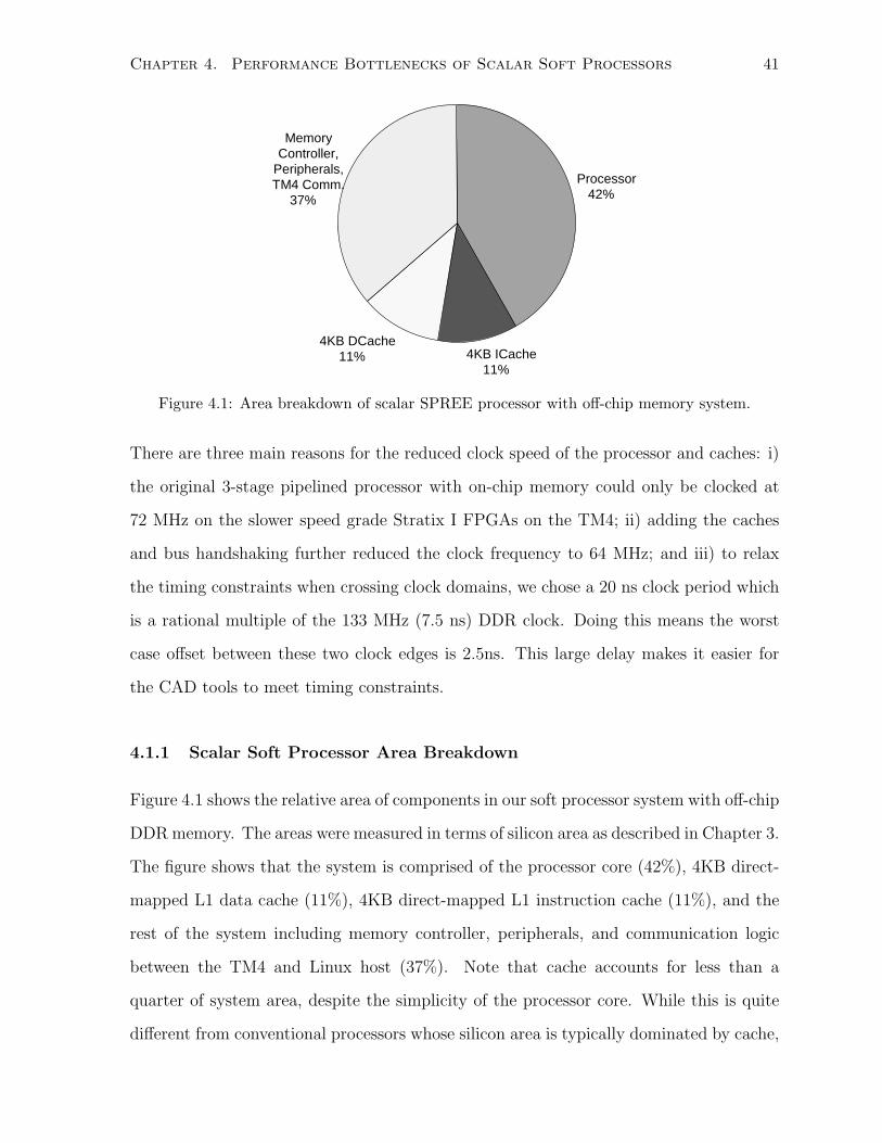
Chapter 4. Performance Bottlenecks of Scalar Soft Processors 41
Processor42%
4KB ICache11%
Memory Controller,
Peripherals, TM4 Comm.
37%
4KB DCache11%
Figure 4.1: Area breakdown of scalar SPREE processor with off-chip memory system.
There are three main reasons for the reduced clock speed of the processor and caches: i)
the original 3-stage pipelined processor with on-chip memory could only be clocked at
72 MHz on the slower speed grade Stratix I FPGAs on the TM4; ii) adding the caches
and bus handshaking further reduced the clock frequency to 64 MHz; and iii) to relax
the timing constraints when crossing clock domains, we chose a 20 ns clock period which
is a rational multiple of the 133 MHz (7.5 ns) DDR clock. Doing this means the worst
case offset between these two clock edges is 2.5ns. This large delay makes it easier for
the CAD tools to meet timing constraints.
4.1.1 Scalar Soft Processor Area Breakdown
Figure 4.1 shows the relative area of components in our soft processor system with off-chip
DDR memory. The areas were measured in terms of silicon area as described in Chapter 3.
The figure shows that the system is comprised of the processor core (42%), 4KB direct-
mapped L1 data cache (11%), 4KB direct-mapped L1 instruction cache (11%), and the
rest of the system including memory controller, peripherals, and communication logic
between the TM4 and Linux host (37%). Note that cache accounts for less than a
quarter of system area, despite the simplicity of the processor core. While this is quite
different from conventional processors whose silicon area is typically dominated by cache,
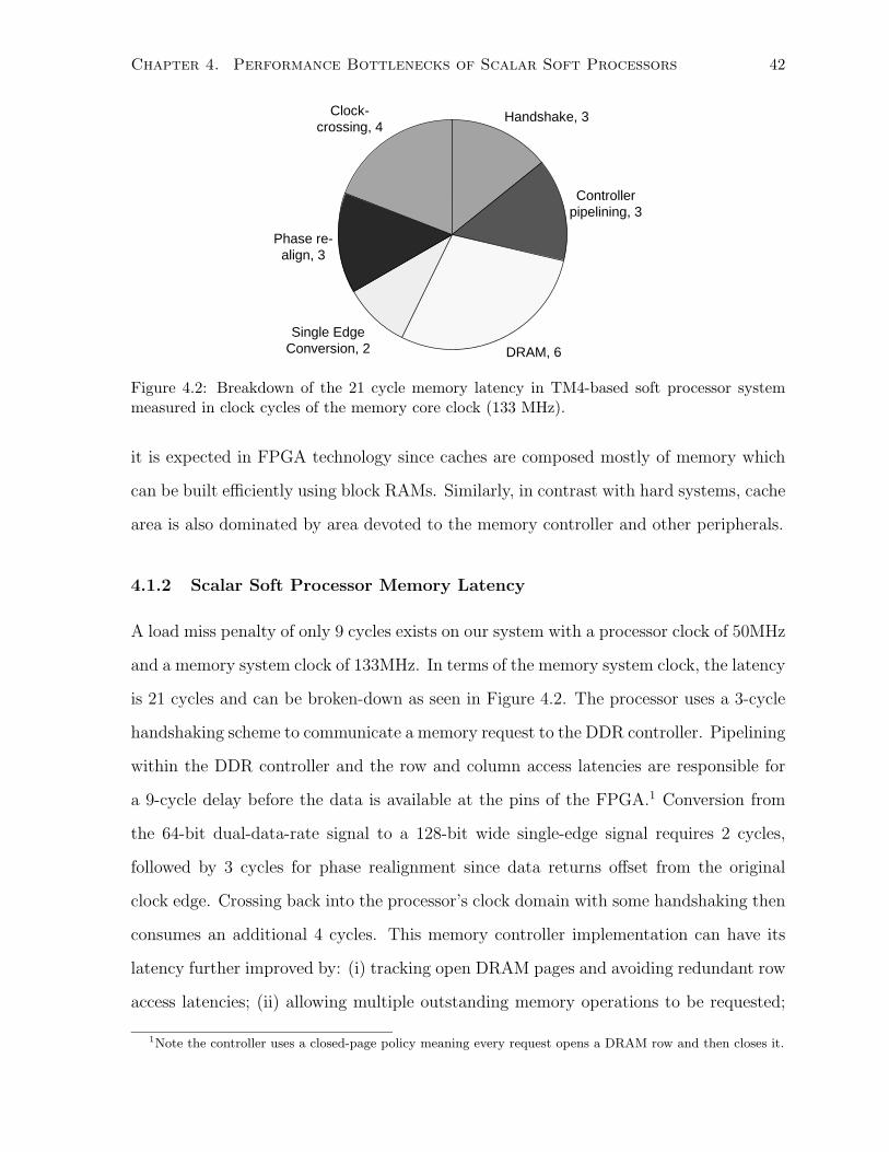
Chapter 4. Performance Bottlenecks of Scalar Soft Processors 42
Controller pipelining, 3
DRAM, 6
Single Edge Conversion, 2
Phase re-align, 3
Clock-crossing, 4
Handshake, 3
Figure 4.2: Breakdown of the 21 cycle memory latency in TM4-based soft processor systemmeasured in clock cycles of the memory core clock (133 MHz).
it is expected in FPGA technology since caches are composed mostly of memory which
can be built efficiently using block RAMs. Similarly, in contrast with hard systems, cache
area is also dominated by area devoted to the memory controller and other peripherals.
4.1.2 Scalar Soft Processor Memory Latency
A load miss penalty of only 9 cycles exists on our system with a processor clock of 50MHz
and a memory system clock of 133MHz. In terms of the memory system clock, the latency
is 21 cycles and can be broken-down as seen in Figure 4.2. The processor uses a 3-cycle
handshaking scheme to communicate a memory request to the DDR controller. Pipelining
within the DDR controller and the row and column access latencies are responsible for
a 9-cycle delay before the data is available at the pins of the FPGA.1 Conversion from
the 64-bit dual-data-rate signal to a 128-bit wide single-edge signal requires 2 cycles,
followed by 3 cycles for phase realignment since data returns offset from the original
clock edge. Crossing back into the processor’s clock domain with some handshaking then
consumes an additional 4 cycles. This memory controller implementation can have its
latency further improved by: (i) tracking open DRAM pages and avoiding redundant row
access latencies; (ii) allowing multiple outstanding memory operations to be requested;
1Note the controller uses a closed-page policy meaning every request opens a DRAM row and then closes it.
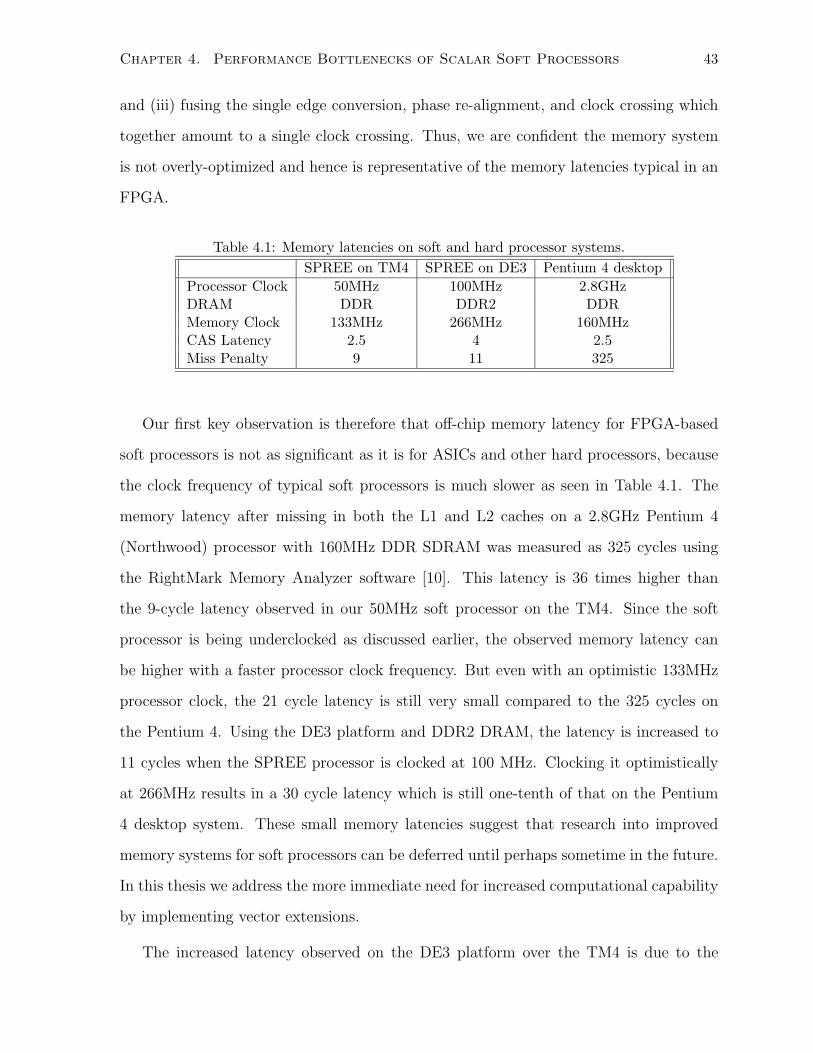
Chapter 4. Performance Bottlenecks of Scalar Soft Processors 43
and (iii) fusing the single edge conversion, phase re-alignment, and clock crossing which
together amount to a single clock crossing. Thus, we are confident the memory system
is not overly-optimized and hence is representative of the memory latencies typical in an
FPGA.
Table 4.1: Memory latencies on soft and hard processor systems.SPREE on TM4 SPREE on DE3 Pentium 4 desktop
Processor Clock 50MHz 100MHz 2.8GHzDRAM DDR DDR2 DDRMemory Clock 133MHz 266MHz 160MHzCAS Latency 2.5 4 2.5Miss Penalty 9 11 325
Our first key observation is therefore that off-chip memory latency for FPGA-based
soft processors is not as significant as it is for ASICs and other hard processors, because
the clock frequency of typical soft processors is much slower as seen in Table 4.1. The
memory latency after missing in both the L1 and L2 caches on a 2.8GHz Pentium 4
(Northwood) processor with 160MHz DDR SDRAM was measured as 325 cycles using
the RightMark Memory Analyzer software [10]. This latency is 36 times higher than
the 9-cycle latency observed in our 50MHz soft processor on the TM4. Since the soft
processor is being underclocked as discussed earlier, the observed memory latency can
be higher with a faster processor clock frequency. But even with an optimistic 133MHz
processor clock, the 21 cycle latency is still very small compared to the 325 cycles on
the Pentium 4. Using the DE3 platform and DDR2 DRAM, the latency is increased to
11 cycles when the SPREE processor is clocked at 100 MHz. Clocking it optimistically
at 266MHz results in a 30 cycle latency which is still one-tenth of that on the Pentium
4 desktop system. These small memory latencies suggest that research into improved
memory systems for soft processors can be deferred until perhaps sometime in the future.
In this thesis we address the more immediate need for increased computational capability
by implementing vector extensions.
The increased latency observed on the DE3 platform over the TM4 is due to the
Chapter 4. Performance Bottlenecks of Scalar Soft Processors 44
Altera DDR2 High Performance Memory Controller used, which is much more sophisti-
cated than the DDR controller we designed ourselves for the TM4. The Altera DDR2
controller supports multiple outstanding memory requests, though our soft processor
does not exploit this as it can service only one memory operation at a time. It also
tracks open DRAM pages, so that a cache misses to an already open page would exhibit
a shorter latency. Finally, the memory controller is aggressively pipelined since it must
satisfy timing constraints in many different designs on many different devices. After
two generations of CMOS technology improvements, this increased latency can at best
suggest a gradual worsening soft processor-memory performance gap. We expect that
going forward, soft processors will continue to observe memory latencies much smaller
than conventional microprocessors. Despite the small memory latencies, the memory
system may be a significant bottleneck in a scalar soft processor if the latency could not
be effectively hidden. This is explored in the subsequent section.
4.2 Scaling Soft Processor Caches
If the memory latency was a significant bottleneck, then hiding that latency would greatly
increase the performance of the system. In this section we explore the impact of cache
configuration on performance to measure the significance of memory latency in our scalar
soft processor system. We extrapolate our results and model an ideal memory system
(effectively on-chip memory) to determine an upper bound on the speedup that could be
achieved by eliminating the memory latency.
In this experiment we use the parameterized data cache depth in our scalar soft
processor to vary the capacity of the cache. This data was collected from an in-hardware
execution of the EEMBC benchmarks on the TM4. The measured line in Figure 4.3 shows
the geometric-mean speedup across our EEMBC benchmarks for varying direct-mapped
data-cache sizes, relative to a 4KB data cache. Compared to the 4KB data cache, an
enormous 256KB data cache provides only a 9% additional speedup at the cost of a

Chapter 4. Performance Bottlenecks of Scalar Soft Processors 45
0.92
1.00
1.061.08 1.09
1.101.12
0.90
0.98
1.04
1.071.08
0.8
0.85
0.9
0.95
1
1.05
1.1
1.15
256B 1KB 4KB 16KB 64KB 256KB 1024KB Perfect
Ave
rag
e S
pee
du
p v
s 4K
B M
od
elle
d
Data Cache Size
Modelled Speedup
Measured Speedup
Figure 4.3: Geometric mean speedup across our EEMBC benchmarks for varying direct-mapped data-cache sizes, relative to a 4KB data cache. Speedup is both measured in realhardware and modeled according to Equation 4.1, both with a 64KB instruction-cache. For themodeled speedup, the perfect point shows the impact of a perfect data cache.
64-fold increase in area devoted to cache.
To extrapolate these results further, we used our hardware system and an instruction
set simulator to derive a model of the system. To model the impact of a given cache, we
use the equation:
Speedup = CPIperfect + (fldMldPld) + (fstMstPst) (4.1)
where CPIperfect is the cycles-per-instruction measured with a perfect memory system,
fld is the frequency of loads, Mld is the load miss rate, Pld is the load miss penalty
in processor cycles. The third term in the equation is analogous to the second and
uses equivalent parameters specifically for stores instead of loads. Using the CPI values
measured previously for our processors with only on-chip memory [70] as an estimate, the
frequency of memory references and miss rates measured using our instruction simulator
as seen in Appendix A, and miss penalties reported by the Altera SignalTap II Logic
Analyzer software, we plot the modelled speedup line shown in Figure 4.3. The figure
shows that the modelled speedup tracks the measured speedup very closely, with the
modelled speedup being slightly larger since it models neither instruction misses nor bus
contention. According to this model a perfect data cache improves performance only

Chapter 4. Performance Bottlenecks of Scalar Soft Processors 46
12% over the 4KB data cache. Caches with increased associativity may be ineffective
at achieving this performance because they would increase the cache access latency.
The diminishing returns seen in the larger cache sizes and the idealized cache point out
that the memory system is not a significant bottleneck. While vector extensions can
also aid in relieving memory bottlenecks, soft processors are uniquely able to adapt to
their memory access patterns to effectively hide memory latency. In a memory bound
system it is likely that this would produce performance scaling with significantly less area
cost than a vector processor. Since soft processors are not presently memory bound we
forego this potentially large research topic and are hence motivated to explore a means
of translating additional area into improved performance other than increasing memory
system performance.
4.3 Soft vs Hard Processor Comparison
Recall that our goal is to use software-programmed soft processors to replace much of
the manual hardware design in an FPGA system. To enable greater capability in soft
processors we also seek performance scaling significantly beyond that achieved by improv-
ing the memory system. To provide a context for these goals, we compare soft processor
performance to hard processor performance. This allows us to approximate the large per-
formance losses associated with implementing a processor on an FPGA substrate. Note
it is not our goal to make FPGAs the desired substrate for all microprocessors, rather,
soft processors are already adequately motivated despite their lack of performance as
discussed below.
An FPGA design which includes a software component can execute that software
on (i) an off-chip hard processor, (ii) an on-chip hard processor such as the PPC 405
included on various Xilinx FPGAs, and (iii) on a soft processor. The first option requires
additional board space and power, the second option raises the costs of FPGAs, while
the soft processor option likely performs the worst. By leveraging the reprogrammability
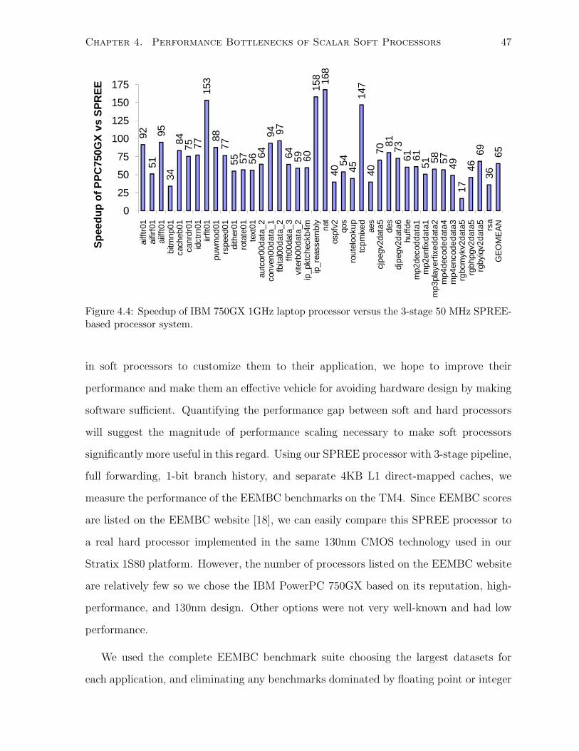
Chapter 4. Performance Bottlenecks of Scalar Soft Processors 47
9251
9534
8475 77
153
8877
55 57 5664
94 9764 59 60
158 16
840
5445
147
4070
8173
61 6151 58 57 49
1746
6936
65
0
25
50
75
100
125
150
175
aifft
r01
aifir
f01
aiiff
t01
bitm
np01
cach
eb01
canr
dr01
idct
rn01
iirflt
01pu
wm
od01
rspe
ed01
dith
er01
rota
te01
text
01au
tcor
00da
ta_2
conv
en00
data
_1fb
ital0
0dat
a_2
fft0
0dat
a_3
vite
rb00
data
_2ip
_pkt
chec
kb4m
ip_r
eass
embl
yna
tos
pfv2 qos
rout
eloo
kup
tcpm
ixed ae
scj
pegv
2dat
a5 des
djpe
gv2d
ata6
huffd
em
p2de
codd
ata1
mp2
enfix
data
1m
p3pl
ayer
fixed
data
2m
p4de
code
dat
a4m
p4en
code
dat
a3rg
bcm
ykv2
data
5rg
bhpg
v2da
ta5
rgby
iqv2
data
5rs
aG
EO
ME
AN
Sp
eed
up
of P
PC
750G
X v
s S
PR
EE
Figure 4.4: Speedup of IBM 750GX 1GHz laptop processor versus the 3-stage 50 MHz SPREE-based processor system.
in soft processors to customize them to their application, we hope to improve their
performance and make them an effective vehicle for avoiding hardware design by making
software sufficient. Quantifying the performance gap between soft and hard processors
will suggest the magnitude of performance scaling necessary to make soft processors
significantly more useful in this regard. Using our SPREE processor with 3-stage pipeline,
full forwarding, 1-bit branch history, and separate 4KB L1 direct-mapped caches, we
measure the performance of the EEMBC benchmarks on the TM4. Since EEMBC scores
are listed on the EEMBC website [18], we can easily compare this SPREE processor to
a real hard processor implemented in the same 130nm CMOS technology used in our
Stratix 1S80 platform. However, the number of processors listed on the EEMBC website
are relatively few so we chose the IBM PowerPC 750GX based on its reputation, high-
performance, and 130nm design. Other options were not very well-known and had low
performance.
We used the complete EEMBC benchmark suite choosing the largest datasets for
each application, and eliminating any benchmarks dominated by floating point or integer

Chapter 4. Performance Bottlenecks of Scalar Soft Processors 48
division operations as our processor did not have hardware support for these operations.
Certain benchmarks such as nat and iirflt01 still contain a significant amount of
division and hence additionally suffer in our system which performs division in software.
Figure 4.4 shows the performance of our SPREE processor against the IBM PowerPC
750GX which was used in laptop computers and greatly outperforms typical embedded
processors. The PPC750GX is a 1GHz out-of-order multi-issue processor with 32KB 4-
way set associative L1 caches, a shared 1MB L2 cache, and a 200 MHz memory bus clock.
On average, the PPC750GX performs 65x faster than our 50 MHz in-order single-issue
processor with separate 4KB direct-mapped caches and a 133-MHz memory clock with
9-cycle memory access latency. The rgbcmyk benchmark is executed only 17x faster
than our soft processor. This datum seems to be an anomaly, but without access to the
PPC750GX or its compiler further investigation is impeded. A likely cause of this are
the conditional statements within the small loop which cannot be accurately predicted
since they are data dependent. Our SPREE processor with its short pipeline is only
slightly affected by mispredicted branches, a more highly aggressive design such as the
PPC750GX may be more heavily impacted.
The large 65x performance gap is in part accounted for by the 20x faster processor
clock speed of the PPC750GX. Differing processor architecture, memory hierarchy, and
memory technology presumably contribute to the remainder of the gap. As we showed
in the last section, idealizing the complete memory system does not significantly increase
the performance of the soft processor. This suggests that soft processors need to be
equipped with far more powerful compute capabilities than currently available, and that
the order of performance gains necessary to truly make soft processors useful beyond
their current niche is in the 10-50x range. Our goal is to make significant progress in this
direction through the use of soft vector processors.
Chapter 4. Performance Bottlenecks of Scalar Soft Processors 49
4.4 Summary
In this chapter we investigated a system comprised of a commercially competitive scalar
soft processor connected to off-chip DDR RAM in real hardware. The observed memory
latency was only 9 cycles, significantly smaller than in traditional hard processors which
are clocked in the GHz range. We noted that the size of a 4KB data cache is just one
quarter the size of the soft processor. We also saw that expanding this cache to 256KB
provided only a 9% increase in performance as measured in hardware, and when we model
an ideal memory system, only 12% better performance is possible. Thus, the small 4KB
direct-mapped cache has largely solved the memory problem for current soft processors
running embedded benchmarks. Further increases to the computational capabilities of
soft processors are necessary to widen their adoption. Against a hard laptop processor
our commercially competitive soft processor was 65x slower with a 20x slower clock rate.
By reducing this gap we hope soft processors will provide a more affordable, simple,
and effective means of implementing computation in FPGAs. Rather than performing
incremental improvements to soft processors, the magnitude of the gap motivates research
into highly scalable soft processor architectures.
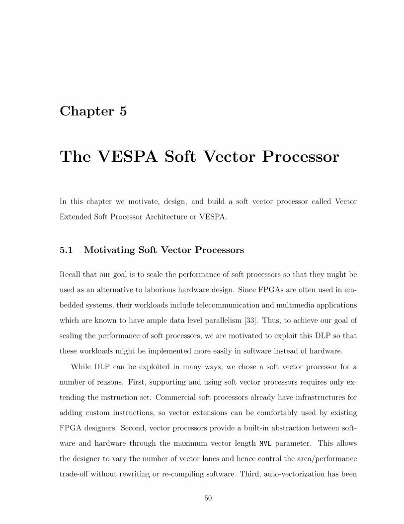
Chapter 5
The VESPA Soft Vector Processor
In this chapter we motivate, design, and build a soft vector processor called Vector
Extended Soft Processor Architecture or VESPA.
5.1 Motivating Soft Vector Processors
Recall that our goal is to scale the performance of soft processors so that they might be
used as an alternative to laborious hardware design. Since FPGAs are often used in em-
bedded systems, their workloads include telecommunication and multimedia applications
which are known to have ample data level parallelism [33]. Thus, to achieve our goal of
scaling the performance of soft processors, we are motivated to exploit this DLP so that
these workloads might be implemented more easily in software instead of hardware.
While DLP can be exploited in many ways, we chose a soft vector processor for a
number of reasons. First, supporting and using soft vector processors requires only ex-
tending the instruction set. Commercial soft processors already have infrastructures for
adding custom instructions, so vector extensions can be comfortably used by existing
FPGA designers. Second, vector processors provide a built-in abstraction between soft-
ware and hardware through the maximum vector length MVL parameter. This allows
the designer to vary the number of vector lanes and hence control the area/performance
trade-off without rewriting or re-compiling software. Third, auto-vectorization has been
50
Chapter 5. The VESPA Soft Vector Processor 51
thoroughly researched and already exists in compilers such as GCC [14] because detecting
the fine-grain data parallelism used by vector processors is far simpler than the gen-
eral parallelization problem. With high-quality auto-vectorization, soft vector processors
could be seamlessly used in a typical C-based design flow and the FPGA designer would
need only to choose the number of lanes depending on the space available on their device.
On going research in auto-vectorization algorithms [50] could help enable this seamless
design flow. Finally, the biggest reason is that a vector architecture is well-suited to
FPGA implementation. A vector processor with all lanes operating in lockstep requires
very little inter-lane coordination making the design scalable in hardware. Moreover, the
architecture does not require any large associative lookups, many ported register files, or
other structures that are inefficient to implement in FPGAs. Other architectures such as
superscalar processors could require such inefficient FPGA structures. For all these rea-
sons we believe soft vector processors can effectively exploit DLP on an FPGA and hence
promote simpler software implementations of components instead of manual hardware
design.
5.2 VESPA Design Goals
In deriving the design goals for VESPA, it is useful to target the computational tasks that
a soft vector processor is likely to be used for. The decision to use a soft vector processor
implementation depends not only on the amount of DLP in a computation, but also on
how critical the given computation is to the overall performance of the system. A digital
system is comprised of many components each implementing different computational
tasks which vary in both their DLP and their performance requirements (or criticality).
Computations with little or no DLP, as well as highly critical computations which justify
highly-optimized hardware design are unsuitable candidates for execution on a soft vector
processor. Thus, as shown in Figure 5.1, the class of computations targeted in this thesis
is low to medium critical computations with sufficient DLP. The benchmarks used in
Chapter 5. The VESPA Soft Vector Processor 52
Criticality
Dat
a P
aral
lelis
m
0
Figure 5.1: A view of the space of computations divided along the axes of DLP and performancecriticality. Computations with low DLP and criticality are near the origin and are likely candi-dates for implementation on a scalar soft processor, while computations with sufficient DLP andlow to medium criticality are shown in grey and are targeted in this thesis for implementationon a soft vector processor.
this thesis typically have very high DLP. Increased amounts of DLP motivate soft vector
processor implementations for more critical computations. As a result the design goals
for VESPA are as follows:
1. Scalability – The more VESPA can scale performance, the more likely it is to be
used for computation with higher criticalities. Since our goal is to reduce the amount
of hardware design, converting these more critical computations into software is key
for this thesis.
2. Flexibility – Aside from the number of lanes, there are several other parameters
that can dramatically affect the area and performance of a soft vector processor.
To exploit the unique ability of FPGAs to quickly implement custom hardware,
VESPA was designed with many architectural parameters which designers can use
to meet their area/performance needs.
3. Portability – Although less crucial than the first two goals, it is also important
that a soft vector processor can be easily ported to different FPGA architectures.

Chapter 5. The VESPA Soft Vector Processor 53
ScalarMIPS
VectorIssue
Lane 1Lane 2
Lane L…
MemoryCrossbar
Dcache
…
Icache
Prefetch
Arbiter
DRAM
Vector Coprocessor
Figure 5.2: VESPA processor system block diagram.
With this property, FPGA vendors and users are more likely to adopt soft vec-
tor processors since maintaining the design across their many FPGA families is
simplified.
To achieve these goals and verify the feasibility of soft vector processors on FPGAs
we implemented VESPA on the FPGA hardware platforms described in Chapter 3.
5.3 VESPA
The VESPA soft vector processor was designed to meet the aforementioned goals. VESPA
is composed of a scalar processor and an attached vector coprocessor. A diagram includ-
ing both components as well as their connection to memory is shown in Figure 5.2. The
figure shows the MIPS-based scalar and VIRAM-based vector coprocessor both fed by
one instruction stream read from the instruction cache. Both cores can execute out-
of-order with respect to each other except for communication and memory instructions
Chapter 5. The VESPA Soft Vector Processor 54
which are serialized to maintain sequential memory consistency. Vector instructions enter
the vector coprocessor, are decoded into element operations which are issued onto the
vector lanes and executed in lockstep. The vector coprocessor and scalar soft processor
share the same data cache and its data prefetcher though the prefetching strategy can
be separately configured for scalar and vector memory accesses. The four sections below
describe the scalar processor, the vector instruction set implemented by the vector co-
processor, the vector coprocessor memory architecture and the VESPA pipeline in more
detail.
5.3.1 MIPS-Based Scalar Processor
The instruction set architecture (ISA) used for our scalar processor core is a subset of
MIPS-I [46] which excludes floating-point, virtual memory, and exception-related instruc-
tions; floating point operations are supported through the use of software libraries. This
subset of MIPS is the set of instructions supported by the SPREE system [70, 71] which
is used to automatically generate our scalar soft processor FPGA implementation in syn-
thesizable Verilog HDL. The generated scalar processor is a 3-stage MIPS-I pipeline with
full forwarding and a 4Kx1-bit branch history table for branch prediction.
The SPREE framework was modified in two ways to better meet the needs of the
vector processor. First, an integer divider unit was added to the SPREE component li-
brary along with instruction support for MIPS divide instructions. This was necessary to
accommodate the fbital benchmark which requires scalar division. Second, to support
the vector coprocessor, the MIPS coprocessor interface instructions were implemented
in SPREE. These instructions allow the SPREE processor to send data to the copro-
cessor and vice versa. With these changes in place we can automatically generate new
scalar processor cores and attach them directly to the memory system and vector copro-
cessor without modification, allowing future studies to consider both scalar and vector
architectures in tandem.
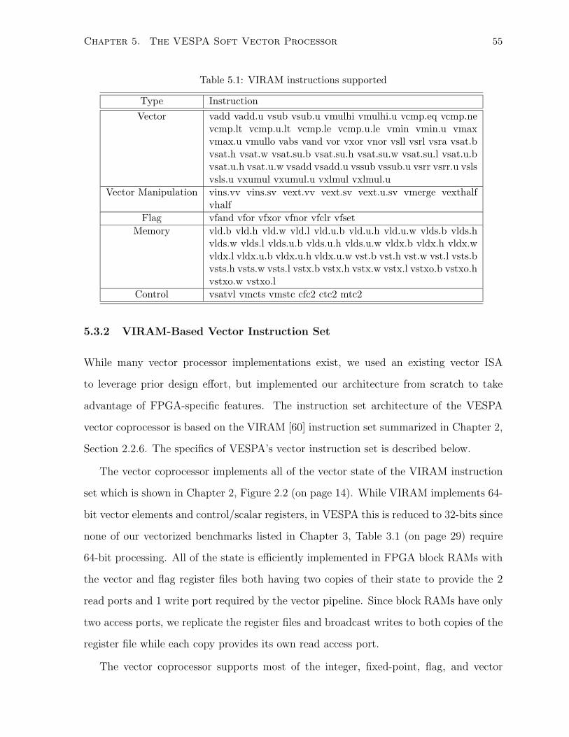
Chapter 5. The VESPA Soft Vector Processor 55
Table 5.1: VIRAM instructions supported
Type InstructionVector vadd vadd.u vsub vsub.u vmulhi vmulhi.u vcmp.eq vcmp.ne
vcmp.lt vcmp.u.lt vcmp.le vcmp.u.le vmin vmin.u vmaxvmax.u vmullo vabs vand vor vxor vnor vsll vsrl vsra vsat.bvsat.h vsat.w vsat.su.b vsat.su.h vsat.su.w vsat.su.l vsat.u.bvsat.u.h vsat.u.w vsadd vsadd.u vssub vssub.u vsrr vsrr.u vslsvsls.u vxumul vxumul.u vxlmul vxlmul.u
Vector Manipulation vins.vv vins.sv vext.vv vext.sv vext.u.sv vmerge vexthalfvhalf
Flag vfand vfor vfxor vfnor vfclr vfsetMemory vld.b vld.h vld.w vld.l vld.u.b vld.u.h vld.u.w vlds.b vlds.h
vlds.w vlds.l vlds.u.b vlds.u.h vlds.u.w vldx.b vldx.h vldx.wvldx.l vldx.u.b vldx.u.h vldx.u.w vst.b vst.h vst.w vst.l vsts.bvsts.h vsts.w vsts.l vstx.b vstx.h vstx.w vstx.l vstxo.b vstxo.hvstxo.w vstxo.l
Control vsatvl vmcts vmstc cfc2 ctc2 mtc2
5.3.2 VIRAM-Based Vector Instruction Set
While many vector processor implementations exist, we used an existing vector ISA
to leverage prior design effort, but implemented our architecture from scratch to take
advantage of FPGA-specific features. The instruction set architecture of the VESPA
vector coprocessor is based on the VIRAM [60] instruction set summarized in Chapter 2,
Section 2.2.6. The specifics of VESPA’s vector instruction set is described below.
The vector coprocessor implements all of the vector state of the VIRAM instruction
set which is shown in Chapter 2, Figure 2.2 (on page 14). While VIRAM implements 64-
bit vector elements and control/scalar registers, in VESPA this is reduced to 32-bits since
none of our vectorized benchmarks listed in Chapter 3, Table 3.1 (on page 29) require
64-bit processing. All of the state is efficiently implemented in FPGA block RAMs with
the vector and flag register files both having two copies of their state to provide the 2
read ports and 1 write port required by the vector pipeline. Since block RAMs have only
two access ports, we replicate the register files and broadcast writes to both copies of the
register file while each copy provides its own read access port.
The vector coprocessor supports most of the integer, fixed-point, flag, and vector
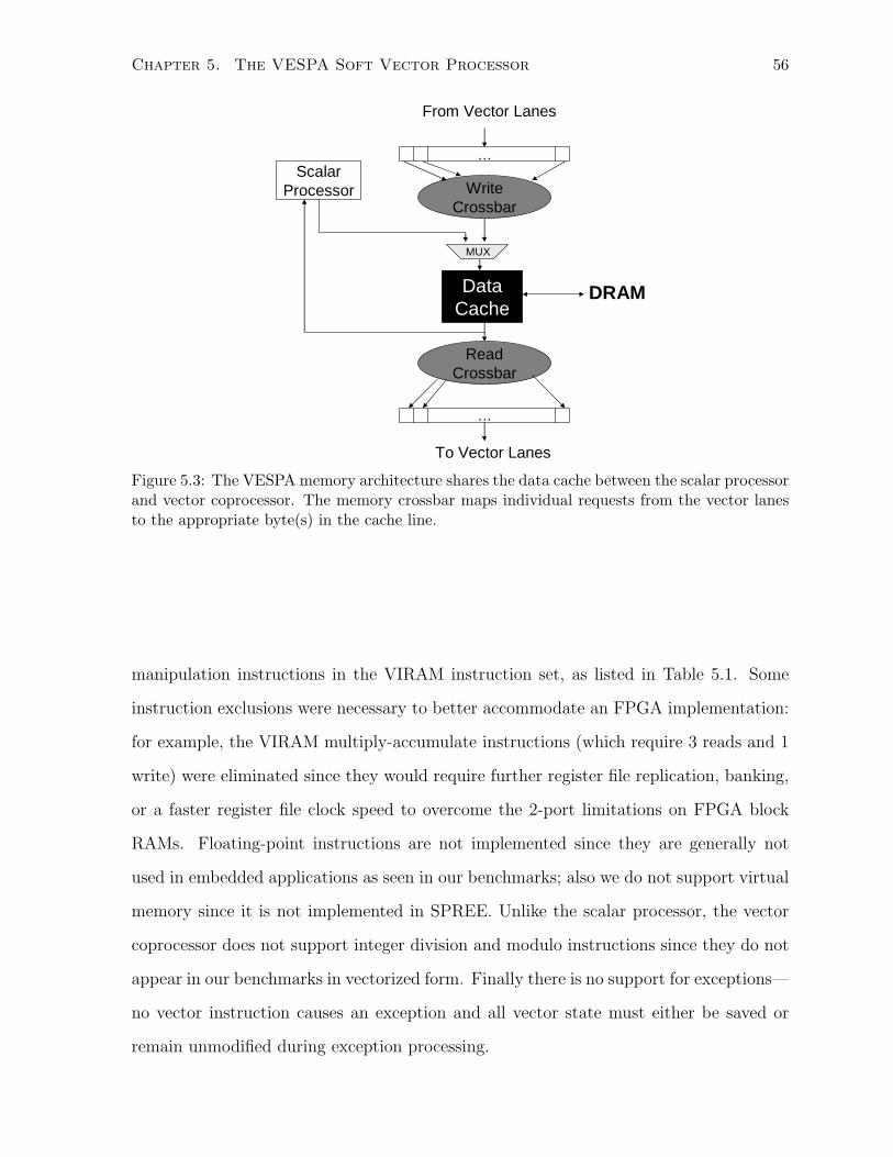
Chapter 5. The VESPA Soft Vector Processor 56
DataCache
WriteCrossbar
ScalarProcessor
ReadCrossbar
…
MUX
…
DRAM
From Vector Lanes
To Vector Lanes
Figure 5.3: The VESPA memory architecture shares the data cache between the scalar processorand vector coprocessor. The memory crossbar maps individual requests from the vector lanesto the appropriate byte(s) in the cache line.
manipulation instructions in the VIRAM instruction set, as listed in Table 5.1. Some
instruction exclusions were necessary to better accommodate an FPGA implementation:
for example, the VIRAM multiply-accumulate instructions (which require 3 reads and 1
write) were eliminated since they would require further register file replication, banking,
or a faster register file clock speed to overcome the 2-port limitations on FPGA block
RAMs. Floating-point instructions are not implemented since they are generally not
used in embedded applications as seen in our benchmarks; also we do not support virtual
memory since it is not implemented in SPREE. Unlike the scalar processor, the vector
coprocessor does not support integer division and modulo instructions since they do not
appear in our benchmarks in vectorized form. Finally there is no support for exceptions—
no vector instruction causes an exception and all vector state must either be saved or
remain unmodified during exception processing.

Chapter 5. The VESPA Soft Vector Processor 57
Dcache
base
stride*0
index0
+MUX
...
stride*1
index1
+MUX +
MUX
MemoryRequestQueue
ReadCrossbar
Memory Lanes=4
rddata0rddata1rddataL-1
wrdata0wrdata1
wrdataL-1...
WriteCrossbar
MemoryWrite
QueueWrite Data
ReadData
stride*(L-1)
indexL-1
Figure 5.4: The VESPA memory unit buffers all memory requests from each lane and satisfiesup to M requests a time from a single cache access. In this example M=4. The black bars showspipeline stages, the grey bars show cycle delays which require pipeline stalls.
5.3.3 Vector Memory Architecture
Figure 5.3 shows the VESPA memory architecture. Each vector lane can request its own
memory address but only one cache line can be accessed at a time which is determined
by the requesting lane with the lowest lane identification number. For example, lane
1 will request its address from the cache then each byte in the accessed cache line can
be simultaneously routed to any lane through the memory crossbar. Thus, the spatial
locality of lane requests is key for fast memory performance since it reduces the number
of cache accesses required to satisfy all lanes. The original VIRAM processor [34] had a
memory crossbar for connecting the lanes to different banks of the on-chip memory. We
use the same concept for connecting the lanes to different words in a cache line. There
is one such crossbar for reads and another for writes; we treat both as one and refer to
the pair as the memory crossbar (with the bidirectionality assumed). This crossbar is
the least scalable structure in the vector processor design but should be configured to
sustain the performance of the memory system it is connected to.
Figure 5.4 shows the vector memory unit in more detail. The black bars indicate
pipeline stages while the grey bars show registers which require pipeline stalls. In the
first stage the addresses being accessed by each lane is computed and loaded into the
Chapter 5. The VESPA Soft Vector Processor 58
Memory Request Queue. The memory unit will then attempt to satisfy up to M of these
lane requests at a time from a single cache access. When all M requests have been satisfied
the Memory Request Queue shifts all its contents up by M. If the instruction is a vector
store, the Memory Write Queue duplicates this behaviour. When the Memory Request
Queue is empty the vector memory unit de-asserts its stall signal and is ready to accept
a new memory operation.
Many options exist for connecting the vector coprocessor to memory, including though
a cache shared with the scalar processor, a separate cache, or no cache. The original VI-
RAM processor used the last approach and was connected directly to its on-chip memory
without a cache. However for off-chip memories caches are more likely required to hide
the memory latencies. While this may not be true for heavily streaming benchmarks, in
some cases the cache may be so important that the vector coprocessor requires its own
separate data cache to avoid competing for cache space with the scalar core. This range
of different memory system configurations could be interesting to explore in the future,
but for this work a shared data cache is used primarily to avoid memory consistency
issues which complicate the design. The decision is further supported for the following
reasons: (i) its low area cost as seen in Section 4.1.1 provides little motivation to avoid
using a cache; (ii) it is certainly required for the scalar core which the vector coprocessor
can “piggyback” on, especially since (iii) there is very little competition for cache space
between the scalar and vector cores in our applications. This decision may need to be
revisited for applications with significant interaction between the scalar and vector cores,
but most of our benchmarks have only a small amount of supportive scalar operations.
The data cache blocks on any access, stalling execution until the transaction has been
completed. The memory controller for the TM4 also blocks on any memory access, while
the Altera DDR2 memory controller for the DE3 allows multiple outstanding requests.
VESPA was not improved to take advantage of this feature since the memory bus used
in commercial soft processors does not support it. In the future more scalable vector
architectures could take advantage of non-blocking memory systems.
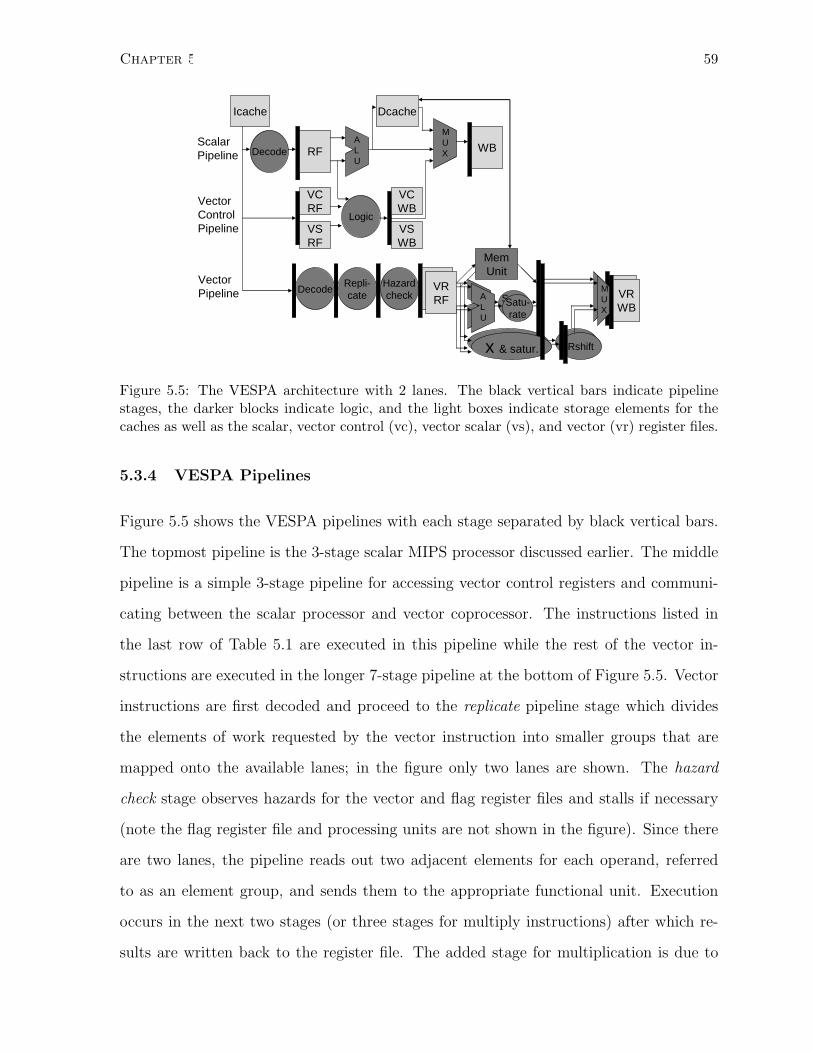
Chapter 5. The VESPA Soft Vector Processor 59
ScalarPipeline
VectorControlPipeline
VectorPipeline
Icache Dcache
Decode RFALU
MUX WB
VCRF
VSRF
VCWB
VSWB
Logic
DecodeRepli-cate
Hazardcheck
VRRF A
LU
x & satur.
VRWB
MUX
Satu-rate
Rshift
VRRF A
LU
x & satur.
VRWB
MUX
Satu-rate
Rshift
MemUnit
Figure 5.5: The VESPA architecture with 2 lanes. The black vertical bars indicate pipelinestages, the darker blocks indicate logic, and the light boxes indicate storage elements for thecaches as well as the scalar, vector control (vc), vector scalar (vs), and vector (vr) register files.
5.3.4 VESPA Pipelines
Figure 5.5 shows the VESPA pipelines with each stage separated by black vertical bars.
The topmost pipeline is the 3-stage scalar MIPS processor discussed earlier. The middle
pipeline is a simple 3-stage pipeline for accessing vector control registers and communi-
cating between the scalar processor and vector coprocessor. The instructions listed in
the last row of Table 5.1 are executed in this pipeline while the rest of the vector in-
structions are executed in the longer 7-stage pipeline at the bottom of Figure 5.5. Vector
instructions are first decoded and proceed to the replicate pipeline stage which divides
the elements of work requested by the vector instruction into smaller groups that are
mapped onto the available lanes; in the figure only two lanes are shown. The hazard
check stage observes hazards for the vector and flag register files and stalls if necessary
(note the flag register file and processing units are not shown in the figure). Since there
are two lanes, the pipeline reads out two adjacent elements for each operand, referred
to as an element group, and sends them to the appropriate functional unit. Execution
occurs in the next two stages (or three stages for multiply instructions) after which re-
sults are written back to the register file. The added stage for multiplication is due to
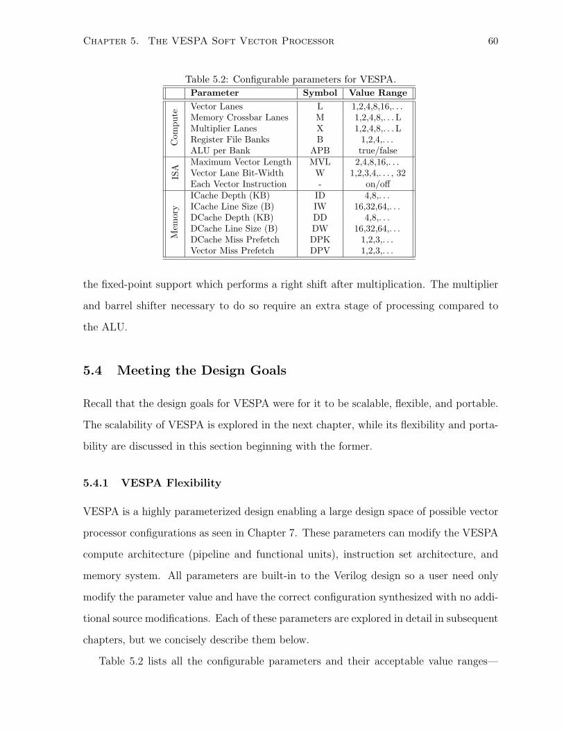
Chapter 5. The VESPA Soft Vector Processor 60
Table 5.2: Configurable parameters for VESPA.Parameter Symbol Value Range
Com
pute
Vector Lanes L 1,2,4,8,16,. . .Memory Crossbar Lanes M 1,2,4,8,. . . LMultiplier Lanes X 1,2,4,8,. . . LRegister File Banks B 1,2,4,. . .ALU per Bank APB true/false
ISA
Maximum Vector Length MVL 2,4,8,16,. . .Vector Lane Bit-Width W 1,2,3,4,. . . , 32Each Vector Instruction - on/off
Mem
ory
ICache Depth (KB) ID 4,8,. . .ICache Line Size (B) IW 16,32,64,. . .DCache Depth (KB) DD 4,8,. . .DCache Line Size (B) DW 16,32,64,. . .DCache Miss Prefetch DPK 1,2,3,. . .Vector Miss Prefetch DPV 1,2,3,. . .
the fixed-point support which performs a right shift after multiplication. The multiplier
and barrel shifter necessary to do so require an extra stage of processing compared to
the ALU.
5.4 Meeting the Design Goals
Recall that the design goals for VESPA were for it to be scalable, flexible, and portable.
The scalability of VESPA is explored in the next chapter, while its flexibility and porta-
bility are discussed in this section beginning with the former.
5.4.1 VESPA Flexibility
VESPA is a highly parameterized design enabling a large design space of possible vector
processor configurations as seen in Chapter 7. These parameters can modify the VESPA
compute architecture (pipeline and functional units), instruction set architecture, and
memory system. All parameters are built-in to the Verilog design so a user need only
modify the parameter value and have the correct configuration synthesized with no addi-
tional source modifications. Each of these parameters are explored in detail in subsequent
chapters, but we concisely describe them below.
Table 5.2 lists all the configurable parameters and their acceptable value ranges—

Chapter 5. The VESPA Soft Vector Processor 61
many integer parameters are limited to powers of two to reduce hardware complexity.
The number of vector lanes (L) determines the number of elements that can be processed
in parallel; this parameter is the most powerful means of scaling the processing power
of VESPA. The width of each vector lane (W) can be adjusted to match the maximum
element size required by the application: by default all lanes are 32-bits wide, but for
some applications 16-bit or even 1-bit wide elements are sufficient. The maximum vector
length (MVL) determines the capacity of the vector register file; hence larger MVL values
allow software to specify greater parallelism in fewer vector instructions, but increases
the register file capacity required in the vector processor.
The number of memory crossbar lanes (M) determines the number of lane memory
requests that can be satisfied concurrently, where 1 < M < L. For example, if M is half
of L, then in Figure 5.3, this means the crossbar connects to half the lanes in one cycle,
and the other half in the next cycle. M is independent of L for two reasons: (i) a crossbar
imposes heavy limitations on the scalability of the design, especially in FPGAs where
the multiplexing used to build the crossbar is comparatively more expensive than for
conventional IC design; and (ii) the cache line size limits the number of lane memory
requests that can be satisfied concurrently. Thus we may not need a full memory crossbar
which routes to all L lanes, rather the parameter M allows the designer to choose a subset
of lanes to route to in a single cycle. This trade-off is explored in Chapter 7, Section 7.1.3.
The user can similarly conserve multiply-accumulate blocks by choosing a subset of
lanes to support multiplication using the X parameter. The B and APB parameters control
the amount of vector chaining VESPA can perform as seen in Chapter 7, Section 7.2.
Also each vector instruction can be individually disabled thereby eliminating the control
logic and datapath support for it as seen in Chapter 7, Section 7.4.
The memory system includes an instruction cache, a data cache, and a data prefetcher.
The instruction cache is direct-mapped with depth ID and cache line size IW. Similarly,
the data cache is direct-mapped with depth DD and cache line size DW. The prefetcher can
be configured with a variety of prefetching schemes which respond to any data access
Chapter 5. The VESPA Soft Vector Processor 62
using DP or exclusively to vector memory operations using DPV. All these memory system
parameters are explored in Chapter 6.
As seen in Chapter 7, the parameters in Table 5.2 provide a large design space for
selecting a custom configuration which best matches the needs of an application. Since
soft processors are readily customizable, we require only software for automatically se-
lecting a configuration for an application. The development of this software is beyond
the scope of this thesis and is hence left as future work.
5.4.2 VESPA Portability
The portability of soft vector processors is a major factor in whether FPGA vendors will
adopt them in the future. Since FPGA vendors have many different FPGA devices and
families, a non-portable hardware IP core would require more design effort to support
across all these devices. The discussion below describes our attempts to minimize the
porting effort.
VESPA is fully implemented in synthesizable Verilog but was purposefully designed to
have no dependencies to a particular FPGA device or family. In fact we ported VESPA
from the Stratix 1S80 on the TM4 to the Stratix III 3S340 on the DE3 and required
zero source modifications. Although we do not port VESPA across different vendors or
families, we instead explain that the FPGA structures needed to efficiently build a soft
vector processor exist in most modern FPGA devices.
To maintain device portability in VESPA, the architected design makes very few
device-specific assumptions. First, it assumes the presence of a full-width multiply oper-
ation which is supported in virtually all modern day FPGA devices and does not assume
any built-in multiply-accumulate or fracturability support since the presence of these
features can vary from device to device. Second, with respect to block RAMs, VESPA
assumes no specific sizes or aspect ratios, nor any particular behaviour for read-during-
write operations on either same or different ports. VESPA only uses one read port and
one write port for any RAM hence limiting the need for bi-directional dual-port RAMs.
Chapter 5. The VESPA Soft Vector Processor 63
These few assumptions allow the VESPA architecture to port to a broad range of FPGA
architectures without re-design. However, although VESPA was not aggressively de-
signed for high clock frequency, any timing decisions made are specific to the Stratix III
it was designed for, hence some device-specific retiming may be needed to achieve high
clock rates on other devices.
5.5 FPGA Influences on VESPA Architecture
Our goal of improving soft processors to compete with hardware design is largely pursued
by matching the architecture to the application. However, soft processors can also be
improved by matching their architectures to the FPGA substrate. Conventional notions
of processor architecture are based on CMOS design, but the tradeoffs on an FPGA sub-
strate can lead to different architectural conclusions. Several previous works considered
the influence of the FPGA substrate on the architecture of soft processors [26, 45, 49, 69].
These works often identify low-level circuit engineering differences but have not proposed
high-level architectural differences between soft and hard processors. Doing so is compli-
cated by two main factors: (i) designer effort and skill varies between academics, FPGA
vendors, and microprocessor companies; and (ii) the level of performance required varies
significantly between soft processors which are used largely as controllers and micropro-
cessors which are used for general purpose computation. As a result, it is difficult to
draw high-level conclusions about the architectures of soft processors since the perfor-
mance attainable on such an architecture is highly dependent on skill, effort, and desired
performance of the designer.
The VESPA architecture was influenced in a number of ways by the FPGA sub-
strate. These influences are discussed in more detail throughout this thesis in sections
devoted to the affected architectural component. We collect the key points and summa-
rize them here. First, the multiply-accumulate blocks are obvious choices for efficiently
implementing processor multipliers. This performance is still significantly less than an
Chapter 5. The VESPA Soft Vector Processor 64
FPGA adder circuit leading to accommodations in the pipeline similar to hard micro-
processors. However, the multipliers are also efficient [45] for implementing shifters since
multiplexers are relatively expensive on FPGAs. This shared multiplier/shifter func-
tional unit means vector chaining on soft vector processors exhibits different behaviour
than traditional vector processors since vector multiplies and vector shifts cannot be ex-
ecuted simultaneously. Second, the block RAMs provide relatively inexpensive storage
helping to motivate the existence of caches even when they are not strongly motivated
in our vectorized applications. The low area cost of storage also helps motivate vector
processors since the large vector register files required can be efficiently implemented.
Finally, the two ports on FPGA block RAMs also impose architectural differences from
traditional processors. For 3-operand instruction sets such as MIPS, the register file must
sustain 2 reads and 1 write per cycle. Since FPGA block RAMs have only two ports, a
common solution is to leverage the low area cost of block RAMs to duplicate them as
discussed in section 5.6. Additional ports are required to support multiple vector instruc-
tion execution. Chapter 7.2 describes how banking is performed to overcome the port
limitations. This approach is reminiscent of vector processors before VLSI design, and
marks a key architectural difference between VESPA and modern vector processors such
as the T0 [7] and VIRAM [34]. In general, the lack of ports and expensive multiplexing
logic make FPGAs less amenable to any architecture with multiple instructions in flight
such as traditional superscalar out-of-order architectures, though it may be possible for
clever circuit engineering by a skilled designer to make such architectures prevalent in
soft processors.
5.6 Selecting a Maximum Vector Length (MVL)
Before further evaluating VESPA we must determine an appropriate maximum vector
length (MVL). This parameter abstracts the number of hardware vector lanes from the
software vector length and hence affects both the hardware implementation of a vector
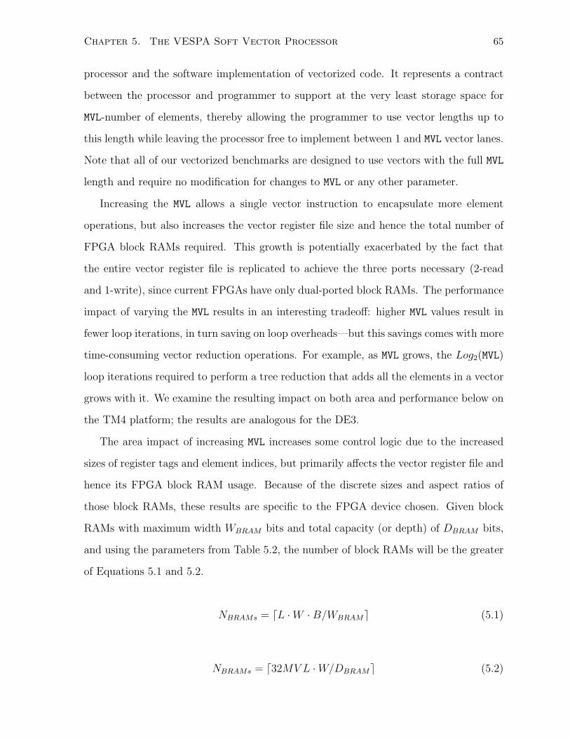
Chapter 5. The VESPA Soft Vector Processor 65
processor and the software implementation of vectorized code. It represents a contract
between the processor and programmer to support at the very least storage space for
MVL-number of elements, thereby allowing the programmer to use vector lengths up to
this length while leaving the processor free to implement between 1 and MVL vector lanes.
Note that all of our vectorized benchmarks are designed to use vectors with the full MVL
length and require no modification for changes to MVL or any other parameter.
Increasing the MVL allows a single vector instruction to encapsulate more element
operations, but also increases the vector register file size and hence the total number of
FPGA block RAMs required. This growth is potentially exacerbated by the fact that
the entire vector register file is replicated to achieve the three ports necessary (2-read
and 1-write), since current FPGAs have only dual-ported block RAMs. The performance
impact of varying the MVL results in an interesting tradeoff: higher MVL values result in
fewer loop iterations, in turn saving on loop overheads—but this savings comes with more
time-consuming vector reduction operations. For example, as MVL grows, the Log2(MVL)
loop iterations required to perform a tree reduction that adds all the elements in a vector
grows with it. We examine the resulting impact on both area and performance below on
the TM4 platform; the results are analogous for the DE3.
The area impact of increasing MVL increases some control logic due to the increased
sizes of register tags and element indices, but primarily affects the vector register file and
hence its FPGA block RAM usage. Because of the discrete sizes and aspect ratios of
those block RAMs, these results are specific to the FPGA device chosen. Given block
RAMs with maximum width WBRAM bits and total capacity (or depth) of DBRAM bits,
and using the parameters from Table 5.2, the number of block RAMs will be the greater
of Equations 5.1 and 5.2.
NBRAMs = �L · W · B/WBRAM� (5.1)
NBRAMs = �32MV L · W/DBRAM� (5.2)
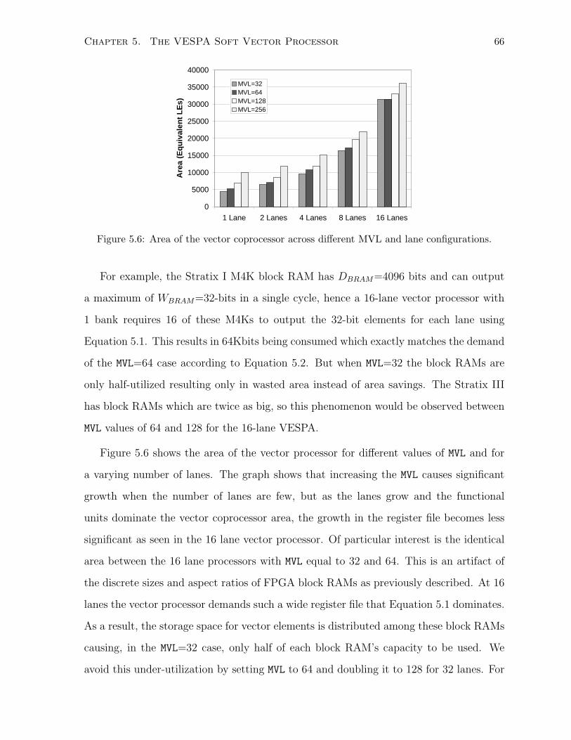
Chapter 5. The VESPA Soft Vector Processor 66
0
5000
10000
15000
20000
25000
30000
35000
40000
1 Lane 2 Lanes 4 Lanes 8 Lanes 16 Lanes
Are
a (E
qu
ival
ent
LE
s)
MVL=32MVL=64MVL=128MVL=256
Figure 5.6: Area of the vector coprocessor across different MVL and lane configurations.
For example, the Stratix I M4K block RAM has DBRAM=4096 bits and can output
a maximum of WBRAM=32-bits in a single cycle, hence a 16-lane vector processor with
1 bank requires 16 of these M4Ks to output the 32-bit elements for each lane using
Equation 5.1. This results in 64Kbits being consumed which exactly matches the demand
of the MVL=64 case according to Equation 5.2. But when MVL=32 the block RAMs are
only half-utilized resulting only in wasted area instead of area savings. The Stratix III
has block RAMs which are twice as big, so this phenomenon would be observed between
MVL values of 64 and 128 for the 16-lane VESPA.
Figure 5.6 shows the area of the vector processor for different values of MVL and for
a varying number of lanes. The graph shows that increasing the MVL causes significant
growth when the number of lanes are few, but as the lanes grow and the functional
units dominate the vector coprocessor area, the growth in the register file becomes less
significant as seen in the 16 lane vector processor. Of particular interest is the identical
area between the 16 lane processors with MVL equal to 32 and 64. This is an artifact of
the discrete sizes and aspect ratios of FPGA block RAMs as previously described. At 16
lanes the vector processor demands such a wide register file that Equation 5.1 dominates.
As a result, the storage space for vector elements is distributed among these block RAMs
causing, in the MVL=32 case, only half of each block RAM’s capacity to be used. We
avoid this under-utilization by setting MVL to 64 and doubling it to 128 for 32 lanes. For
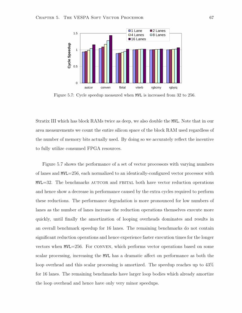
Chapter 5. The VESPA Soft Vector Processor 67
0
0.5
1
1.5
autcor conven fbital viterb rgbcmy rgbyiq
Cyc
le S
pee
du
p
1 Lane 2 Lanes4 Lanes 8 Lanes16 Lanes
Figure 5.7: Cycle speedup measured when MVL is increased from 32 to 256.
Stratix III which has block RAMs twice as deep, we also double the MVL. Note that in our
area measurements we count the entire silicon space of the block RAM used regardless of
the number of memory bits actually used. By doing so we accurately reflect the incentive
to fully utilize consumed FPGA resources.
Figure 5.7 shows the performance of a set of vector processors with varying numbers
of lanes and MVL=256, each normalized to an identically-configured vector processor with
MVL=32. The benchmarks autcor and fbital both have vector reduction operations
and hence show a decrease in performance caused by the extra cycles required to perform
these reductions. The performance degradation is more pronounced for low numbers of
lanes as the number of lanes increase the reduction operations themselves execute more
quickly, until finally the amortization of looping overheads dominates and results in
an overall benchmark speedup for 16 lanes. The remaining benchmarks do not contain
significant reduction operations and hence experience faster execution times for the longer
vectors when MVL=256. For conven, which performs vector operations based on some
scalar processing, increasing the MVL has a dramatic affect on performance as both the
loop overhead and this scalar processing is amortized. The speedup reaches up to 43%
for 16 lanes. The remaining benchmarks have larger loop bodies which already amortize
the loop overhead and hence have only very minor speedups.

Chapter 5. The VESPA Soft Vector Processor 68
5.7 Summary
This chapter described the VESPA soft vector processor which was built to evaluate the
concept of vector processors for FPGAs using off-chip memory systems on real FPGAs
and executing industry-standard embedded benchmarks. VESPA is a complete hardware
design of a scalar MIPS processor and a VIRAM vector coprocessor written in Verilog.
Only a portion of the VIRAM vector instruction set is supported by VESPA which is
described in this chapter. VESPA has many parameterized architectural parameters
briefly summarized here but more thoroughly explored in later chapters. The MVL is one
such parameter explored in this chapter.
Chapter 6
Scalability of the VESPA Soft
Vector Processor
The key goal of this work is to achieve performance significantly beyond current soft
processors to make it easier to leverage the computational power of FPGAs without
complicated hardware design. The scalability of a vector processor is potentially a pow-
erful method of doing so. In this chapter we evaluate whether this scalability holds true
on FPGAs and improve it by exploring the area and performance of several architectural
modifications.
6.1 Initial Scalability (L)
To highlight and quantify the importance of the architectural modifications subsequently
proposed in this research, we first measure the scalability of a base initial design which
lacks these features. Specifically, the initial VESPA design is identical to that described
in Chapter 5 but supported only parameterization of the number of lanes and the MVL
value (which is set to 64 for this scalability study). Its memory system was hard-coded
with two 4KB direct-mapped instruction and data caches each with 16B lines sizes. This
section evaluates the scalability of this design and presents those findings as measured
across the EEMBC benchmarks executed on the TM4 hardware platform. Note that the
69
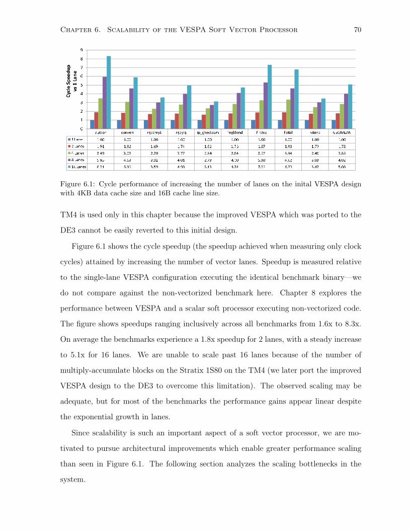
Chapter 6. Scalability of the VESPA Soft Vector Processor 70
autcor conven rgbcmyk rgbyiq ip_checksum imgblend filt3x3 fbital viterb GEOMEAN
1 Lane 1.00 1.00 1.00 1.00 1.00 1.00 1.00 1.00 1.00 1.00
2 Lanes 1.91 1.82 1.69 1.74 1.62 1.76 1.87 1.89 1.73 1.78
4 Lanes 3.49 3.09 2.29 2.77 2.34 2.84 3.27 3.34 2.49 2.85
8 Lanes 5.95 4.63 3.02 4.01 2.73 4.10 5.30 4.62 3.03 4.02
16 Lanes 8.31 5.89 3.59 4.98 3.13 4.74 7.32 6.79 3.47 5.08
0
1
2
3
4
5
6
7
8
9
Cycle Speedup
vs 1 Lane
Figure 6.1: Cycle performance of increasing the number of lanes on the inital VESPA designwith 4KB data cache size and 16B cache line size.
TM4 is used only in this chapter because the improved VESPA which was ported to the
DE3 cannot be easily reverted to this initial design.
Figure 6.1 shows the cycle speedup (the speedup achieved when measuring only clock
cycles) attained by increasing the number of vector lanes. Speedup is measured relative
to the single-lane VESPA configuration executing the identical benchmark binary—we
do not compare against the non-vectorized benchmark here. Chapter 8 explores the
performance between VESPA and a scalar soft processor executing non-vectorized code.
The figure shows speedups ranging inclusively across all benchmarks from 1.6x to 8.3x.
On average the benchmarks experience a 1.8x speedup for 2 lanes, with a steady increase
to 5.1x for 16 lanes. We are unable to scale past 16 lanes because of the number of
multiply-accumulate blocks on the Stratix 1S80 on the TM4 (we later port the improved
VESPA design to the DE3 to overcome this limitation). The observed scaling may be
adequate, but for most of the benchmarks the performance gains appear linear despite
the exponential growth in lanes.
Since scalability is such an important aspect of a soft vector processor, we are mo-
tivated to pursue architectural improvements which enable greater performance scaling
than seen in Figure 6.1. The following section analyzes the scaling bottlenecks in the
system.
Chapter 6. Scalability of the VESPA Soft Vector Processor 71
6.1.1 Analyzing the Initial Design
Assuming a fully data parallel workload with a constant stream of vector instructions
(which closely represents many of our benchmarks), poor scaling can be caused by either
inefficiencies in the vector pipeline or the memory system. Since VESPA executes vector
ALU operations without any wasted cycles it is therefore the vector memory instructions
inhibiting the performance scaling. The vector memory unit stalls one cycle upon re-
ceiving any memory request and then stalls for each necessary cache access. In addition
cache misses result in cycle stalls for the duration of the memory access latency. In this
section we evaluate whether the memory system is indeed throttling the scalability in
VESPA.
The impact of the memory system is measured using cycle-accurate RTL simulation of
the complete VESPA system including the DDR memory controller for four of the bench-
marks1 using the Modelsim simulation infrastructure described in Chapter 3. Hardware
counters were inserted into the design to count the number of cycles the vector memory
unit is stalled, as well as the number of cycles it is stalled due specifically to a cache miss.
Our measurements demonstrate that this initial VESPA design with 16 lanes, 16B
data cache line size and 4KB depth spends approximately 67% of all cycles stalling in
the vector memory unit, and 45% of all cycles servicing data misses. This cache line
size was selected for the initial configuration because it matches the 128-bit width of the
DRAM interface—cache lines smaller than 16B would waste memory bandwidth. The
4KB depth is then selected to fully utilize the capacity of the block RAMs used to create
the 16B line size. Depths less than 4KB (for the Stratix I) would waste FPGA RAM
storage bits because of the discrete aspect ratios of the block RAMs. The large number
of cycles spent in the vector memory unit, and specifically the misses, suggests that the
memory system is significantly throttling VESPA’s performance.
1The other benchmarks are not included because their data sets are too large for simulation
Chapter 6. Scalability of the VESPA Soft Vector Processor 72
6.2 Improving the Memory System
Standard solutions for improving memory system performance include optimizing the
cache configuration and the implementation of an accurate data prefetching strategy. We
pursue these same solutions within VESPA but with an appreciation for the application-
dependence of these solutions since in a soft processor context, an FPGA designer can
select a cache and prefetcher to match their specific application. The data cache is hence
parameterized along its depth (or capacity) and its line size, while a data prefetcher is
implemented with parameterized prefetching strategies.
6.2.1 Cache Design Trade-Offs (DD and DW)
The most obvious approach to increasing memory system performance is to alter the
cache configuration to better hide the memory latency. In this section we parameterize
and explore the speed/area trade-offs for different data cache configurations for direct-
mapped caches. Set-associative caches require multiplexing between the entries in a set,
which is expensive especially in an FPGA and hence deters us from including this option
in our initial exploration. Also, banking the cache was not explored since all of our
benchmarks use mostly contiguous memory accesses. We vary data cache depth from
4KB to 64KB and the cache line size from 16B to 128B. Note, our system experiences
some timing problems caused by the large size of the memory crossbar on the TM4 for a
cache line size of 128B which limits the measurements we can make for that configuration
and cache lines greater than 128B.
Some conclusions from this study can be hypothesized with further examination of the
benchmarks. Many of our vectorized benchmarks are streaming in nature with little data
re-use. For such benchmarks we anticipate that cache depth will not impact performance
significantly while widening the cache line and hence increasing the likelihood of finding
needed data in a single cache access may considerably improve performance. In addition,
the longer cache lines provide some inherent prefetching by caching larger blocks of
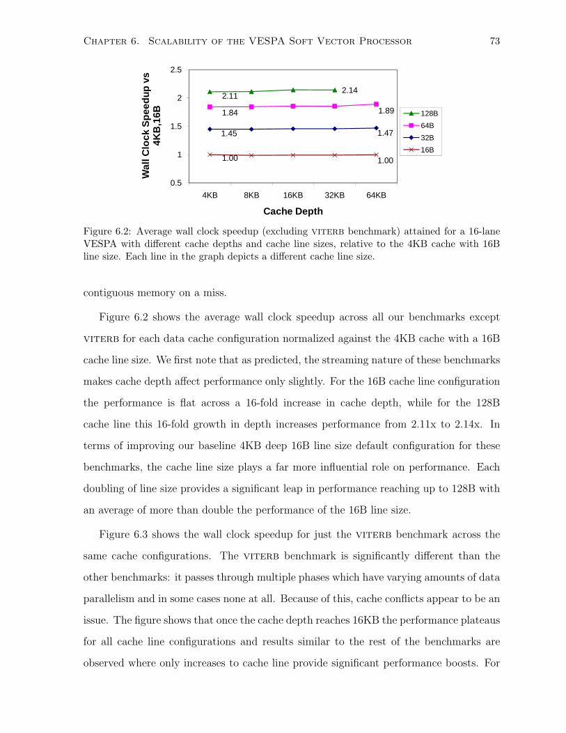
Chapter 6. Scalability of the VESPA Soft Vector Processor 73
2.112.14
1.84 1.89
1.45 1.47
1.00 1.00
0.5
1
1.5
2
2.5
4KB 8KB 16KB 32KB 64KB
Wal
l Clo
ck S
pee
du
p v
s 4K
B,1
6B
Cache Depth
128B
64B
32B
16B
Figure 6.2: Average wall clock speedup (excluding viterb benchmark) attained for a 16-laneVESPA with different cache depths and cache line sizes, relative to the 4KB cache with 16Bline size. Each line in the graph depicts a different cache line size.
contiguous memory on a miss.
Figure 6.2 shows the average wall clock speedup across all our benchmarks except
viterb for each data cache configuration normalized against the 4KB cache with a 16B
cache line size. We first note that as predicted, the streaming nature of these benchmarks
makes cache depth affect performance only slightly. For the 16B cache line configuration
the performance is flat across a 16-fold increase in cache depth, while for the 128B
cache line this 16-fold growth in depth increases performance from 2.11x to 2.14x. In
terms of improving our baseline 4KB deep 16B line size default configuration for these
benchmarks, the cache line size plays a far more influential role on performance. Each
doubling of line size provides a significant leap in performance reaching up to 128B with
an average of more than double the performance of the 16B line size.
Figure 6.3 shows the wall clock speedup for just the viterb benchmark across the
same cache configurations. The viterb benchmark is significantly different than the
other benchmarks: it passes through multiple phases which have varying amounts of data
parallelism and in some cases none at all. Because of this, cache conflicts appear to be an
issue. The figure shows that once the cache depth reaches 16KB the performance plateaus
for all cache line configurations and results similar to the rest of the benchmarks are
observed where only increases to cache line provide significant performance boosts. For

Chapter 6. Scalability of the VESPA Soft Vector Processor 74
0.5
1
1.5
2
2.5
4KB 8KB 16KB 32KB 64KB
Wal
l Clo
ck S
pee
du
p v
s 4K
B,1
6B
Cache Depth
128B
64B
32B
16B
Figure 6.3: Wall clock speedup of viterb benchmark attained for a 16-lane VESPA withdifferent cache depths and cache line sizes, relative to the 4KB cache with 16B line size. Eachline in the graph depicts a different cache line size.
Table 6.1: Clock frequency of different cache line sizes for a 16-lane VESPA.Cache Line Size (B) Clock Frequency (MHz)
16B 128 MHz32B 127 MHz64B 123 MHz128B 122 MHz
4KB cache depths, increasing the cache line size past 32B actually decreases performance.
For an 8KB cache the same phenomenon occurs at 64B instead. In both cases the cause is
increased conflicts since with constant depth, a wider cache line size creates fewer cache
sets. Unlike the other benchmarks, viterb has significant data re-use and capturing
that working set in a 16KB cache is imperative before applying further memory system
improvements.
In contrast with the scalar soft processors shown in Chapter 4, the increase in com-
putational power via multiple lanes in the vector processor makes the memory system
more influential in determining overall performance. Chapter 4 demonstrated that the
impact of the memory system is limited to 12% additional performance for the scalar soft
processor, whereas in both Figure 6.2 and Figure 6.3 performance is more than doubled.
Table 6.1 shows that the clock frequency is slightly reduced as the cache line size
increases. This clock frequency degradation is due to the multiplexing needed to get data

Chapter 6. Scalability of the VESPA Soft Vector Processor 75
0
0.2
0.4
0.6
0.8
1
1.2
1.4
1.6
1.8
2
16B 32B 64B 128B
Cache Line Size
No
rmal
ized
Sys
tem
Are
a
4KB8KB16KB32KB64KB
Figure 6.4: System area of different cache configurations on a 16-lane VESPA normalizedagainst the 4KB cache with 16B line size. Each coloured bar in the graph depicts a differentcache depth.
words out of the large cache lines and into the vector lanes via the memory crossbar.
In other words, by doubling the cache line size, the memory crossbar is also doubled in
size and is responsible for the frequency degradation. Further logic design effort through
pipelining and retiming can mitigate these effects, resulting in slightly more pronounced
benefits for the longer cache lines.
Figure 6.4 shows the silicon area of the VESPA system normalized against that of
the 4KB cache with 16B line size. The area cost can be quite significant, in the worst
case almost doubling the system area. However, the area trends are quite different than
what one would expect with traditional hard processors. We discuss the effect on area
of cache depth and cache line size below.
Increases in cache depth have a minimal effect on area and in many cases are hidden
by the noise in the synthesis algorithms: for example, the 4KB cache with 64B line size
is larger than its 8KB counterpart. This is a synthesis anomaly since the number of
block RAMs and multiply-accumulate blocks is the same for both designs, yet the 4KB
configuration consumes 900 additional LEs. In fact all caches with a 64B line size have
the same number of block RAMs except for the 64KB depth configuration, in which case
the added block RAMs for cache depth does not contribute significantly more area than

Chapter 6. Scalability of the VESPA Soft Vector Processor 76
16
bits4096
bits16
bits4096
bits16
bits4096
bits16
bits4096
bits16
bits4096
bits16
bits4096
bits16
bits4096
bits16
bits4096
bits
128 bit cache line size
4KB cache depth
Figure 6.5: Multiple block RAMs are needed to create the width necessary for 16B cache lines,and the cache depth should be 4KB to fully-utilize the capacity of those block RAMs.
the rest of the 64B configurations. Such results are expected for an FPGA since cache
depth only affects the block-RAM storage required, which is more efficiently implemented
relative to programmable logic.
Increasing the cache line size can also increase the number of block RAMs consumed.
Certainly the largest contributor to the increased area with cache line size is the multi-
plexers in the vector memory crossbar which routes each byte to each vector lane; however
it is also due to the increase in FPGA block RAMs being used, a phenomenon unique
to FPGAs. In their current configuration, the block RAMs are limited to a maximum
of 16-bit wide data ports: to create a cache with 16B (128-bit) line sizes we require at
least 8 such FPGA block RAMs in parallel, as shown in Figure 6.5, hence consuming all
8 of those block RAMs and their associated silicon area. Any increases in cache line sizes
will result in corresponding increases in the number of used block RAMs and with it an
automatic increase of physical storage bits used (whether they are logically used by the
design or not). Therefore we generally choose the depth to fill the capacity of the fewest
number of block RAMs required to satisfy the line size.
In terms of supporting VESPA configurations with many lanes, such as the 16-lane
configuration used throughout this section, we believe the 40% additional area is worth
the performance increase of a data cache with 64 byte line size and 16KB depth to fill the
used block RAMs. The two factors that contribute to these performance improvements
are: (i) wider cache lines require fewer cache accesses to satisfy memory requests from
all the lanes; and (ii) wider cache lines bring larger blocks of neighbouring data into
Chapter 6. Scalability of the VESPA Soft Vector Processor 77
the cache on a miss providing effective prefetching for our streaming benchmarks which
access data sequentially. Of course, the latter benefit can be achieved through hardware
prefetching which comes without significant area cost.
6.2.2 Impact of Data Prefetching (DPK and DPV)
Due to the predictable memory access patterns in our benchmarks, we can automatically
prefetch data needed by the application before the data is requested. We hence augment
VESPA by supporting hardware data prefetching where a cache miss translates into a
request for the missing cache line as well as additional cache lines that are predicted
to soon be accessed. This section describes the data prefetcher in VESPA as well as
evaluates its effect across our benchmarks.
6.2.2.1 Prefetching Background
Data prefetching is a topic thoroughly studied in the computer architecture commu-
nity [63]. The simplest scheme, known as sequential prefetching, fetches the missed cache
line as well as the next K cache lines in memory. All our prefetching schemes are based
on sequential prefetching since this maps well to our many streaming benchmarks.
Fu and Patel had investigated prefetching particularly in the context of a vector
processor [22]. They limited prefetching to vector memory instructions with strides
less than or equal to cache line size and found that prefetching is generally useful for
up to 32 cache blocks. But in an FPGA context we can appreciate the application-
dependent nature of prefetching since the FPGA-system can be reconfigured with a
custom prefetcher configuration. We further experiment with a vector length prefetch
where the vector length is used to calculate the number of cache lines to prefetch.
6.2.2.2 Designing a Prefetcher
The data prefetcher is configured using the parameters DPK and DPV from Table 5.2.
DPK is the number of consecutive cache lines prefetched on any cache miss—note that
Chapter 6. Scalability of the VESPA Soft Vector Processor 78
prefetching is triggered for both scalar and vector instructions since both share the same
data cache and its prefetcher. To minimize cache pollution we introduce a copy of that
parameter, DPV, to prefetch specifically for vector instructions having strides within two
cache lines (as done by Fu and Patel [22]) which can be prefetched more aggressively since
they are known to access the cache sequentially. We refer to these misses as sequential
vector misses.
A key advantage of the data prefetcher is that it leverages the high bandwidth from
burst mode transfers; after an initial miss penalty, all cache lines including the prefetched
lines are streamed into the cache at the full DDR rate. This bandwidth is vital for
VESPA which processes batches of memory requests for each vector memory instruction.
Complications arise from handling such large memory transfers when the evicted cache
lines are dirty. To ensure that these dirty lines are properly written-back to memory we
must either drop the prefetched line, or else buffer the dirty cache lines and write them
back to memory later; this write back buffer approach is used in VESPA, and prefetching
is halted when the 2KB buffer is full. For simplicity, we also halted prefetching at the
end of the DRAM row that the miss initially accessed.
The prefetcher is currently limited to working only with cache lines greater than
or equal to 64B. With smaller cache lines the prefetcher has fewer cycles between the
loading of successive cache lines to probe the cache entries and decide whether to allow
the prefetch or not. For example if a cache entry is dirty and a prefetch request seeks
to replace it with a stale copy of its data from memory, that prefetch must be blocked.
As a result we use only 64B cache lines and 16KB depth to fully-utilize the block RAM
capacity. As mentioned previously, cache line sizes of 128B and larger are unstable in
our design so we are confined to evaluating prefetching on only the 64B line size.
6.2.2.3 Cache Line Size and Prefetching
As discussed in Section 6.2.1, in general we expect wider cache lines to perform some
inherent prefetching and hence reduce the impact of our hardware prefetcher. Conversely,
Chapter 6. Scalability of the VESPA Soft Vector Processor 79
hardware prefetching can have more impact on narrower cache lines. Hence, one can
reduce area by shrinking the cache line size (and with it the large memory crossbar)
while using hardware prefetching to explicitly perform the inherent data prefetching of
longer cache lines. However, the long cache lines are typically required to capture more
of the spatial locality that is used to satisfy multiple lane requests. Without it more
cache accesses (and hence cycles) are required to satisfy the lane requests.
6.2.2.4 Evaluating Prefetching
This section explores the impact of the different data prefetching configurations. The
aggressiveness of the prefetcher is increased by doubling the number of cache lines it
loads and is varied using both the DPK and DPV parameters from 0 (no prefetching) to
63 (enough prefetching to fill one quarter of the data cache). As discussed earlier, our
sequential prefetcher can be activated by either (i) any cache miss or (ii) only sequentially-
accessing vector memory instructions; however, our benchmarks generally use very few
scalar loads and stores, and generally have vector strides of less than a cache line, thus
nearly all memory operations are initiated by sequential vector instructions. We therefore
anticipate that both of these activation strategies will perform similarly.
Figure 6.6 shows the performance of prefetching on either any cache miss or sequen-
tial vector misses, both normalized against the performance without prefetching. Using
the same base vector architecture of 16 lanes and full memory crossbar, we configure the
data cache with 16KB depth and 64B line size and explore the impact of the different
data prefetching configurations. The figure shows that, as expected, whether prefetching
is performed on all cache misses or just on known sequential vector instructions, the per-
formance is very similar—they essentially overlap in the graph. The speedup achieved
is quite significant, almost reaching 30% average faster performance. As we increase the
number of cache lines prefetched, and hence the aggressiveness of the prefetcher, we see
diminishing returns on the performance gains until the cache pollution dominates, reduc-
ing the speedup at 63 cache line prefetches. Note that we found that the implementation

Chapter 6. Scalability of the VESPA Soft Vector Processor 80
0.70
0.80
0.90
1.00
1.10
1.20
1.30
0 1 3 7 15 31 63
Number of Cache Lines Prefetched
Sp
eed
up
Any Cache Misses
Sequential Vector only
Figure 6.6: Average speedup, relative to no prefetching, of prefetching n cache lines using twostrategies: (i) on any data cache miss; (ii) on any miss from a sequentially-accessing vectormemory instruction (called sequential vector miss). While the number of prefetched cache linescan be any integer, we selected prefetches such that the total number of cache lines fetchedincluding the missed cache line is a power of two.
of the prefetcher did not impact clock frequency.
Figure 6.7 shows the performance of each benchmark as the aggressiveness is increased
for prefetches triggered by any cache miss. The graph shows that four of the benchmarks,
autcor, conven, viterb, and fbital do not benefit significantly from prefetching,
while the other benchmarks achieve speedups as high as 2.2x. For large prefetches the
performance tapers off and then begins a downward trend as cache pollution begins to
dominate. In the case of conven and fbital the performance becomes worse than with
no prefetching. As long as the number of cache lines being prefetched is moderate, we
can speed up benchmarks that benefit from prefetching without slowing down bench-
marks that do not. On average we observe a peak 30% performance improvement when
prefetching 31 cache lines. Of course the benefit of using a soft vector processor is that
one can tune the amount of prefetching for each application. For example, 15 is often
the best number of cache lines to prefetch on average, but for imgblend prefetching 15
cache lines performs worse than many other configurations.
With respect to area, the cost of prefetching is relatively small requiring mostly control
logic for tracking and issuing multiple successive memory requests. But additional area

Chapter 6. Scalability of the VESPA Soft Vector Processor 81
0.5
1
1.5
2
2.5
0 1 3 7 15 31 63
Number of Cache Lines Prefetched
Sp
eed
up
vs
no
Pre
fetc
hin
g
autcorconvenviterbfbitalrgbcmykrgbyiqip_checksumimgblendfilt3x3GMEAN
Figure 6.7: Speedup when prefetching a constant number of consecutive cache lines on any datacache miss, relative to no-prefetching.
is required by the writeback buffer which stores the evicted dirty cache lines. In general
the buffer needs to have the greater of DPK+1 or DPV+1 entries for the case where all
evicted lines are dirty. With prefetching disabled this cost is reduced to a single register,
but otherwise is generally implemented in FPGA block RAMs where the effect of discrete
aspect ratios as discussed in Figure 6.5 results in a constant 1.6% area cost if prefetching
is between 1 and 15 cache lines. For more than 15 cache lines this area cost doubles, but
there is little additional performance gain seen in our benchmarks to justify the added
area cost.
6.2.2.5 Vector Length Prefetching
Choosing a good value for the amount of prefetching, DPK, depends on the mix of vector
lengths used in the program. Recall each vector memory instruction instance explicitly
specifies its vector length providing a valuable hint for the number of cache lines to
prefetch. In this section our goal is to make use of this hint to achieve a high quality
prefetch configuration without requiring a brute force exploration. We therefore recast
DPK as DPV which is a multiplier of the current vector length. Note that the actual vector
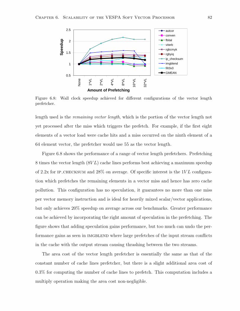
Chapter 6. Scalability of the VESPA Soft Vector Processor 82
0.5
1
1.5
2
2.5
Non
e
1*V
L
2*V
L
4*V
L
8*V
L
16*V
L
32*V
L
Sp
eed
up
Amount of Prefetching
autcor
conven
fbital
viterb
rgbcmyk
rgbyiq
ip_checksum
imgblend
filt3x3
GMEAN
Figure 6.8: Wall clock speedup achieved for different configurations of the vector lengthprefetcher.
length used is the remaining vector length, which is the portion of the vector length not
yet processed after the miss which triggers the prefetch. For example, if the first eight
elements of a vector load were cache hits and a miss occurred on the ninth element of a
64 element vector, the prefetcher would use 55 as the vector length.
Figure 6.8 shows the performance of a range of vector length prefetchers. Prefetching
8 times the vector length (8V L) cache lines performs best achieving a maximum speedup
of 2.2x for ip checksum and 28% on average. Of specific interest is the 1V L configura-
tion which prefetches the remaining elements in a vector miss and hence has zero cache
pollution. This configuration has no speculation, it guarantees no more than one miss
per vector memory instruction and is ideal for heavily mixed scalar/vector applications,
but only achieves 20% speedup on average across our benchmarks. Greater performance
can be achieved by incorporating the right amount of speculation in the prefetching. The
figure shows that adding speculation gains performance, but too much can undo the per-
formance gains as seen in imgblend where large prefetches of the input stream conflicts
in the cache with the output stream causing thrashing between the two streams.
The area cost of the vector length prefetcher is essentially the same as that of the
constant number of cache lines prefetcher, but there is a slight additional area cost of
0.3% for computing the number of cache lines to prefetch. This computation includes a
multiply operation making the area cost non-negligible.
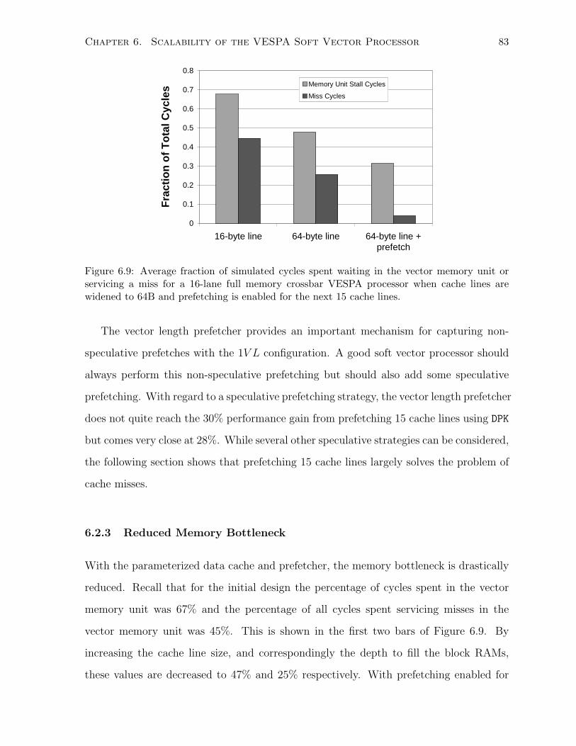
Chapter 6. Scalability of the VESPA Soft Vector Processor 83
0
0.1
0.2
0.3
0.4
0.5
0.6
0.7
0.8
16-byte line 64-byte line 64-byte line +prefetch
Fra
ctio
n o
f T
ota
l Cyc
les Memory Unit Stall Cycles
Miss Cycles
Figure 6.9: Average fraction of simulated cycles spent waiting in the vector memory unit orservicing a miss for a 16-lane full memory crossbar VESPA processor when cache lines arewidened to 64B and prefetching is enabled for the next 15 cache lines.
The vector length prefetcher provides an important mechanism for capturing non-
speculative prefetches with the 1V L configuration. A good soft vector processor should
always perform this non-speculative prefetching but should also add some speculative
prefetching. With regard to a speculative prefetching strategy, the vector length prefetcher
does not quite reach the 30% performance gain from prefetching 15 cache lines using DPK
but comes very close at 28%. While several other speculative strategies can be considered,
the following section shows that prefetching 15 cache lines largely solves the problem of
cache misses.
6.2.3 Reduced Memory Bottleneck
With the parameterized data cache and prefetcher, the memory bottleneck is drastically
reduced. Recall that for the initial design the percentage of cycles spent in the vector
memory unit was 67% and the percentage of all cycles spent servicing misses in the
vector memory unit was 45%. This is shown in the first two bars of Figure 6.9. By
increasing the cache line size, and correspondingly the depth to fill the block RAMs,
these values are decreased to 47% and 25% respectively. With prefetching enabled for
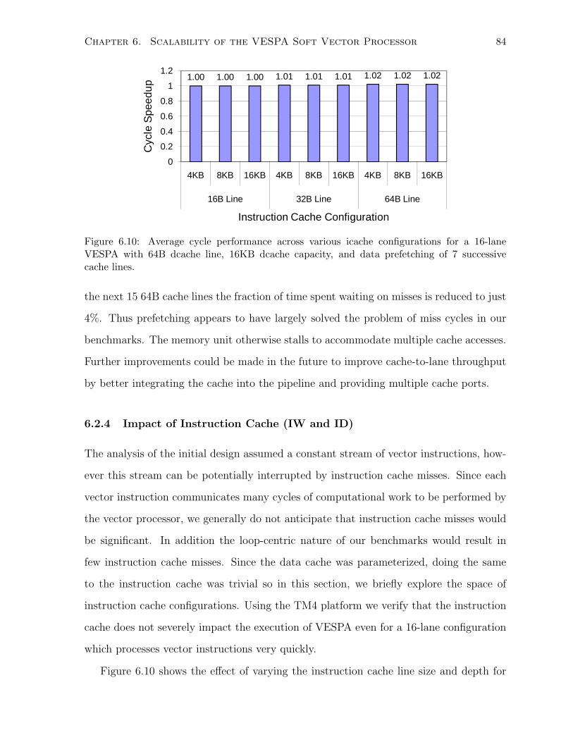
Chapter 6. Scalability of the VESPA Soft Vector Processor 84
1.00 1.00 1.00 1.01 1.01 1.01 1.02 1.02 1.02
0
0.2
0.4
0.6
0.8
1
1.2
4KB 8KB 16KB 4KB 8KB 16KB 4KB 8KB 16KB
16B Line 32B Line 64B Line
Cyc
le S
peed
up
Instruction Cache Configuration
Figure 6.10: Average cycle performance across various icache configurations for a 16-laneVESPA with 64B dcache line, 16KB dcache capacity, and data prefetching of 7 successivecache lines.
the next 15 64B cache lines the fraction of time spent waiting on misses is reduced to just
4%. Thus prefetching appears to have largely solved the problem of miss cycles in our
benchmarks. The memory unit otherwise stalls to accommodate multiple cache accesses.
Further improvements could be made in the future to improve cache-to-lane throughput
by better integrating the cache into the pipeline and providing multiple cache ports.
6.2.4 Impact of Instruction Cache (IW and ID)
The analysis of the initial design assumed a constant stream of vector instructions, how-
ever this stream can be potentially interrupted by instruction cache misses. Since each
vector instruction communicates many cycles of computational work to be performed by
the vector processor, we generally do not anticipate that instruction cache misses would
be significant. In addition the loop-centric nature of our benchmarks would result in
few instruction cache misses. Since the data cache was parameterized, doing the same
to the instruction cache was trivial so in this section, we briefly explore the space of
instruction cache configurations. Using the TM4 platform we verify that the instruction
cache does not severely impact the execution of VESPA even for a 16-lane configuration
which processes vector instructions very quickly.
Figure 6.10 shows the effect of varying the instruction cache line size and depth for

Chapter 6. Scalability of the VESPA Soft Vector Processor 85
Listing 6.1: Vectorized ip checksum loop
LOOP:vld . u . h vr0 , vbase0 , v inc1 # Vectorvadd . u vr1 , vr1 , vr0 # Vectorc tc2 r2 , v l # Vector Ctlv s a tv l # Vector Ctlsub r2 , r2 , r14 # Sca la rbgtz r2 ,LOOP # Sca la r
a 16-lane VESPA with a 16KB data cache with 64B lines and hardware prefetching of
the 7 neighbouring cache lines. The results show at most 2% performance gain averaged
across our benchmarks. This is somewhat expected since many of the benchmarks are
streaming in nature and spend most of the execution time iterating in one or a few loops.
The system area cost of the largest 16KB-64B configuration is 10% greater than the
4KB-16B configuration. Although this cost is much smaller than seen in the data cache
(due to the memory crossbar which is not required for instructions), the performance
improvement is too small to justify this area cost. All configurations in this thesis use
the 4KB instruction cache with 16B line size.
6.3 Decoupling Vector and Control Pipelines
The assumption of a constant stream of vector instructions is also violated in practice
by the presence of scalar code and vector control instructions. The scalar pipeline was
decoupled from the vector coprocessor in the initial design meaning cycles spent pro-
cessing scalar code can be done while the vector coprocessor is busy processing vector
instructions. But the vector coprocessor must still stall for vector control instructions
to complete. As more lanes are added to VESPA, less time is spent processing vector
instructions causing these vector control operations to possibly become significant. In
this section we examine the effect of also decoupling the vector control pipeline allowing
out-of-order execution between all three pipelines shown in Chapter 5, Figure 5.5. This
optimization was motivated by visual inspection of the benchmark discussed below.
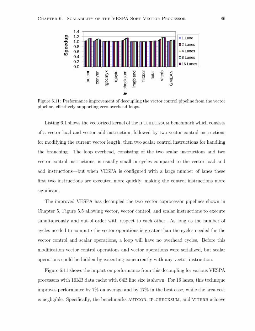
Chapter 6. Scalability of the VESPA Soft Vector Processor 86
0.00.20.40.60.81.01.21.4
autc
or
conv
en
rgbc
myk
rgby
iq
ip_c
heck
sum
imgb
lend
filt3
x3
fbita
l
vite
rb
GM
EA
N
Sp
eed
up 1 Lane
2 Lanes
4 Lanes
8 Lanes
16 Lanes
Figure 6.11: Performance improvement of decoupling the vector control pipeline from the vectorpipeline, effectively supporting zero-overhead loops.
Listing 6.1 shows the vectorized kernel of the ip checksum benchmark which consists
of a vector load and vector add instruction, followed by two vector control instructions
for modifying the current vector length, then two scalar control instructions for handling
the branching. The loop overhead, consisting of the two scalar instructions and two
vector control instructions, is usually small in cycles compared to the vector load and
add instructions—but when VESPA is configured with a large number of lanes these
first two instructions are executed more quickly, making the control instructions more
significant.
The improved VESPA has decoupled the two vector coprocessor pipelines shown in
Chapter 5, Figure 5.5 allowing vector, vector control, and scalar instructions to execute
simultaneously and out-of-order with respect to each other. As long as the number of
cycles needed to compute the vector operations is greater than the cycles needed for the
vector control and scalar operations, a loop will have no overhead cycles. Before this
modification vector control operations and vector operations were serialized, but scalar
operations could be hidden by executing concurrently with any vector instruction.
Figure 6.11 shows the impact on performance from this decoupling for various VESPA
processors with 16KB data cache with 64B line size is shown. For 16 lanes, this technique
improves performance by 7% on average and by 17% in the best case, while the area cost
is negligible. Specifically, the benchmarks autcor, ip checksum, and viterb achieve
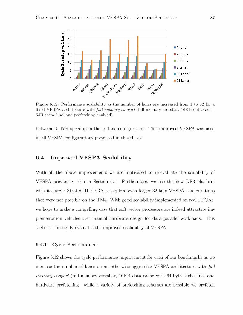
Chapter 6. Scalability of the VESPA Soft Vector Processor 87
0
5
10
15
20
25
30
Cycle Speedup vs 1 Lane
1 Lane
2 Lanes
4 Lanes
8 Lanes
16 Lanes
32 Lanes
Figure 6.12: Performance scalability as the number of lanes are increased from 1 to 32 for afixed VESPA architecture with full memory support (full memory crossbar, 16KB data cache,64B cache line, and prefetching enabled).
between 15-17% speedup in the 16-lane configuration. This improved VESPA was used
in all VESPA configurations presented in this thesis.
6.4 Improved VESPA Scalability
With all the above improvements we are motivated to re-evaluate the scalability of
VESPA previously seen in Section 6.1. Furthermore, we use the new DE3 platform
with its larger Stratix III FPGA to explore even larger 32-lane VESPA configurations
that were not possible on the TM4. With good scalability implemented on real FPGAs,
we hope to make a compelling case that soft vector processors are indeed attractive im-
plementation vehicles over manual hardware design for data parallel workloads. This
section thoroughly evaluates the improved scalability of VESPA.
6.4.1 Cycle Performance
Figure 6.12 shows the cycle performance improvement for each of our benchmarks as we
increase the number of lanes on an otherwise aggressive VESPA architecture with full
memory support (full memory crossbar, 16KB data cache with 64-byte cache lines and
hardware prefetching—while a variety of prefetching schemes are possible we prefetch
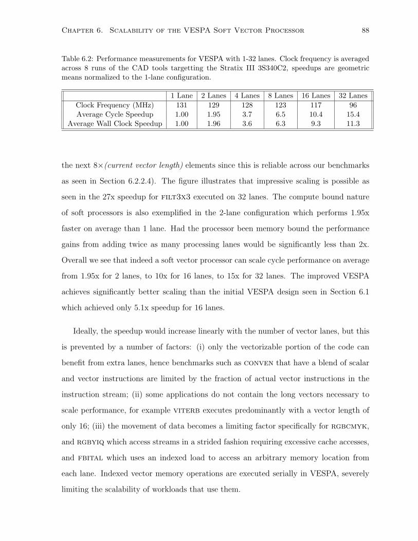
Chapter 6. Scalability of the VESPA Soft Vector Processor 88
Table 6.2: Performance measurements for VESPA with 1-32 lanes. Clock frequency is averagedacross 8 runs of the CAD tools targetting the Stratix III 3S340C2, speedups are geometricmeans normalized to the 1-lane configuration.
1 Lane 2 Lanes 4 Lanes 8 Lanes 16 Lanes 32 LanesClock Frequency (MHz) 131 129 128 123 117 96Average Cycle Speedup 1.00 1.95 3.7 6.5 10.4 15.4
Average Wall Clock Speedup 1.00 1.96 3.6 6.3 9.3 11.3
the next 8×(current vector length) elements since this is reliable across our benchmarks
as seen in Section 6.2.2.4). The figure illustrates that impressive scaling is possible as
seen in the 27x speedup for filt3x3 executed on 32 lanes. The compute bound nature
of soft processors is also exemplified in the 2-lane configuration which performs 1.95x
faster on average than 1 lane. Had the processor been memory bound the performance
gains from adding twice as many processing lanes would be significantly less than 2x.
Overall we see that indeed a soft vector processor can scale cycle performance on average
from 1.95x for 2 lanes, to 10x for 16 lanes, to 15x for 32 lanes. The improved VESPA
achieves significantly better scaling than the initial VESPA design seen in Section 6.1
which achieved only 5.1x speedup for 16 lanes.
Ideally, the speedup would increase linearly with the number of vector lanes, but this
is prevented by a number of factors: (i) only the vectorizable portion of the code can
benefit from extra lanes, hence benchmarks such as conven that have a blend of scalar
and vector instructions are limited by the fraction of actual vector instructions in the
instruction stream; (ii) some applications do not contain the long vectors necessary to
scale performance, for example viterb executes predominantly with a vector length of
only 16; (iii) the movement of data becomes a limiting factor specifically for rgbcmyk,
and rgbyiq which access streams in a strided fashion requiring excessive cache accesses,
and fbital which uses an indexed load to access an arbitrary memory location from
each lane. Indexed vector memory operations are executed serially in VESPA, severely
limiting the scalability of workloads that use them.

Chapter 6. Scalability of the VESPA Soft Vector Processor 89
6.4.2 Clock Frequency
While the cycle performance was shown to be very scalable, in an FPGA context we
can verify that the processor clock speed degradation caused by instantiating more lanes
does not nullify or overwhelm the cycle improvements. In general as a hardware design
grows in size it becomes more challenging to architect and design the circuit to achieve
a high clock frequency. Our measurements of clock frequency on the VESPA architec-
ture demonstrate that a vector processor implemented on an FPGA can retain scalable
performance without whole design teams to optimize the architecture and circuit design.
Certainly VESPA could further benefit from such optimizations.
Table 6.2 shows the clock frequency for each configuration produced by the FPGA
CAD tools as described in Chapter 3. The clock frequency starts at 131 MHz for the
1 lane, decays to 123 MHz for 8 lanes, 117 MHz for 16 lanes, and finally 96 MHz for
32 lanes. The effect on wall clock time is moderate at 16 lanes reducing the 10x cycle
speedup to 9x in actual wall clock time speedup. At 32 lanes the clock frequency drops
significantly reducing the 15x cycle speedup to 11x in wall clock time. Despite these
clock frequency reductions, the average wall clock time across our benchmarks continues
to increase with more lanes. At 64 lanes the clock frequency is reduced to 80 MHz and
the performance is worse than the 32-lane configuration. Because of timing problems
with the 64-lane configuration, it cannot be accurately benchmarked and is hence not
shown in Table 6.2.
In both the 16 and 32 lane configurations, the critical path is in the memory crossbar
which routes all 64 bytes in a cache line to each of the lanes. The M parameter can be
used to reduce the size of the crossbar and raise the clock frequency, but the resultant loss
in average cycle performance often overwhelms this gain and produces a slower overall
processor as shown in Chapter 7, Section 7.1.3. The clock frequency reduction can instead
be addressed by pipelining the memory crossbar as well as additional engineering effort
in retiming these large designs. Ultimately scaling to larger lanes requires careful design
of a high-performing memory system, and may require a hierarchy of memory storage
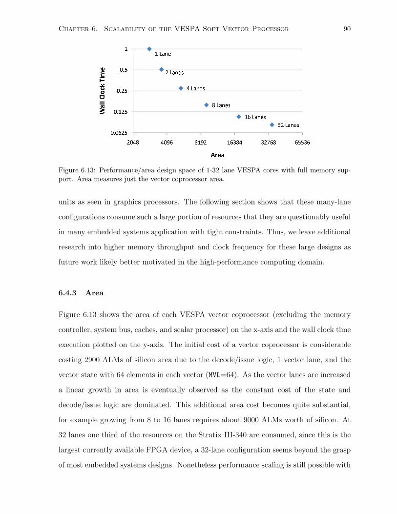
Chapter 6. Scalability of the VESPA Soft Vector Processor 90
1 Lane
2 Lanes
4 Lanes
8 Lanes
16 Lanes
32 Lanes
0.0625
0.125
0.25
0.5
1
2048 4096 8192 16384 32768 65536
Wall Clock Time
Area
Figure 6.13: Performance/area design space of 1-32 lane VESPA cores with full memory sup-port. Area measures just the vector coprocessor area.
units as seen in graphics processors. The following section shows that these many-lane
configurations consume such a large portion of resources that they are questionably useful
in many embedded systems application with tight constraints. Thus, we leave additional
research into higher memory throughput and clock frequency for these large designs as
future work likely better motivated in the high-performance computing domain.
6.4.3 Area
Figure 6.13 shows the area of each VESPA vector coprocessor (excluding the memory
controller, system bus, caches, and scalar processor) on the x-axis and the wall clock time
execution plotted on the y-axis. The initial cost of a vector coprocessor is considerable
costing 2900 ALMs of silicon area due to the decode/issue logic, 1 vector lane, and the
vector state with 64 elements in each vector (MVL=64). As the vector lanes are increased
a linear growth in area is eventually observed as the constant cost of the state and
decode/issue logic are dominated. This additional area cost becomes quite substantial,
for example growing from 8 to 16 lanes requires about 9000 ALMs worth of silicon. At
32 lanes one third of the resources on the Stratix III-340 are consumed, since this is the
largest currently available FPGA device, a 32-lane configuration seems beyond the grasp
of most embedded systems designs. Nonetheless performance scaling is still possible with
Chapter 6. Scalability of the VESPA Soft Vector Processor 91
32-lanes and likely beyond with additional processor design effort.
6.5 Summary
This chapter first demonstrated the modest scalability in a naive VESPA design. Mod-
ified caches, hardware prefetching, and decoupled pipelines were then added to achieve
significantly more scaling. Wider cache lines were the most significant improvement since
they provide some inherent prefetching and also allows a single cache access to satisfy
multiple lanes assuming spatial locality between the memory requests in the lanes. How-
ever the cost of increasing cache lines is large due to the growing memory crossbar.
Prefetching can provide drastically reduced miss rates for a very low area cost, but its
effectiveness is application-dependent. Finally the decoupled vector control pipeline al-
lowed vector control instructions to be executed in parallel with vectorized work. Overall,
the improved VESPA achieved significant scaling of up to 27x for 32 lanes and on average
15x. The next chapter will demonstrate that more thorough exploration of soft vector
processor architecture can yield an even larger and more fine-grain VESPA design space.
Chapter 7
Expanding and Exploring the
VESPA Design Space
One of the most compelling features of soft processors is their inherent reconfigurability.
An FPGA designer can ideally choose the exact soft processor architecture for their
application rather than be limited to a few off-the-shelf variants. If the application
changes, a designer can easily reconfigure a new soft processor onto the FPGA device. In
addition, the designer need not modify the software toolchain, which is often necessary
with the purchase of a new hard processor in an embedded system.
The previous chapter explored a variety of architectural parameters of the VESPA
soft vector processor including the number of lanes, the cache configurations, and the
prefetching strategy. All of these parameters can be tuned to match an application with
respect to its amount of data parallelism and memory access patterns. In this chapter we
explore the computational capability of VESPA, specifically the functional units in its
vector lanes. These functional units can significantly impact the performance of VESPA
and also account for a significant amount of overall area especially when multiple lanes
are present. Thus we explore architectural parameters that allow an FPGA designer to
tune the functional units to their application in three aspects: (i) reducing the number
of functional units in low demand hence creating heterogeneous lanes [74]; (ii) param-
92
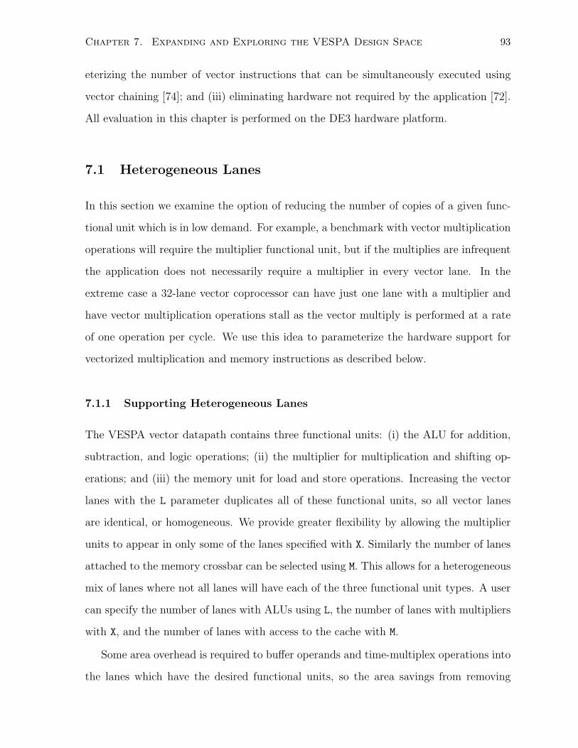
Chapter 7. Expanding and Exploring the VESPA Design Space 93
eterizing the number of vector instructions that can be simultaneously executed using
vector chaining [74]; and (iii) eliminating hardware not required by the application [72].
All evaluation in this chapter is performed on the DE3 hardware platform.
7.1 Heterogeneous Lanes
In this section we examine the option of reducing the number of copies of a given func-
tional unit which is in low demand. For example, a benchmark with vector multiplication
operations will require the multiplier functional unit, but if the multiplies are infrequent
the application does not necessarily require a multiplier in every vector lane. In the
extreme case a 32-lane vector coprocessor can have just one lane with a multiplier and
have vector multiplication operations stall as the vector multiply is performed at a rate
of one operation per cycle. We use this idea to parameterize the hardware support for
vectorized multiplication and memory instructions as described below.
7.1.1 Supporting Heterogeneous Lanes
The VESPA vector datapath contains three functional units: (i) the ALU for addition,
subtraction, and logic operations; (ii) the multiplier for multiplication and shifting op-
erations; and (iii) the memory unit for load and store operations. Increasing the vector
lanes with the L parameter duplicates all of these functional units, so all vector lanes
are identical, or homogeneous. We provide greater flexibility by allowing the multiplier
units to appear in only some of the lanes specified with X. Similarly the number of lanes
attached to the memory crossbar can be selected using M. This allows for a heterogeneous
mix of lanes where not all lanes will have each of the three functional unit types. A user
can specify the number of lanes with ALUs using L, the number of lanes with multipliers
with X, and the number of lanes with access to the cache with M.
Some area overhead is required to buffer operands and time-multiplex operations into
the lanes which have the desired functional units, so the area savings from removing
Chapter 7. Expanding and Exploring the VESPA Design Space 94
0
0.2
0.4
0.6
0.8
1
1.2
Cycle Speedup
X=1 (Area=0.87)
X=2 (Area=0.87)
X=4 (Area=0.88)
X=8 (Area=0.9)
X=16 (Area=0.94)
X=32 (Area=1)
Figure 7.1: Performance impact of varying X for a VESPA with L=32, M=16, DW=64, DD=16K,and DPV=8*VL, area and performance is normalized to the X=32 configuration.
multipliers and shrinking the crossbar must offset this. In place of the missing functional
units are shift registers for shifting input operands to the necessary lane and shifting
back the result. Because of the frequency of ALU operations across the benchmarks and
because of their relative size compare to the overhead, we do not support the elision of
ALUs. This is a reasonable limitation since the multipliers are generally scarce, and the
memory crossbar generally large, so reducing those units will have greater impact on area
savings while being more likely to only mildly affect performance.
7.1.2 Impact of Multiplier Lanes (X)
The X parameter determines the number of lanes with multiplier units. The effect of
varying X is evaluated on a 32-lane VESPA processor with 16 memory crossbar lanes
(halved to reduce its area dominance) and a prefetching 16KB data cache with 64B line
size. Each halving of X doubles the number of cycles needed to complete a vector multiply.
We measure the overall cycle performance and area and normalize it to the full X=32
configuration. Note that clock frequency was unaffected in these designs.
Figure 7.1 shows that in some benchmarks such as filt3x3 the performance degra-
dation is dramatic, while in other benchmarks such as conven there is no impact at all.
Chapter 7. Expanding and Exploring the VESPA Design Space 95
Programs with no vector multiplies can have multipliers removed completely with the
instruction-set subsetting technique explored in Section 7.4.3, but programs with just few
multiplies such as viterb can have its multipliers reduced saving 10% area and suffering
a small 3.1% performance penalty. The resulting saved area can then be used for other
architectural features or components of the system.
The area savings from reducing the multipliers is small starting at 6% for halving
the number of multipliers to 16, the savings asymptotically grow and saturate at 13%.
Since the multipliers are efficiently implemented in the FPGA as a dedicated block,
the contribution to the overall silicon area is small, and the additional overhead for
multiplexing operations into the few lanes with multipliers ultimately outweigh the area
savings. However, multipliers are often found in short supply, so a designer might be
willing to accept the performance penalty if another more critical computation could
benefit from using the multipliers.
7.1.3 Impact of Memory Crossbar (M)
A vector load/store instruction can perform as many memory requests in parallel as the
there are vector lanes, however the data cache can service only one cache line access per
clock cycle. Extracting the data in a cache line to/from each vector lane requires a full
and bidirectional crossbar between every byte in a cache line and every vector lane. Such
a circuit structure imposes heavy limitations on the scalability of the design, especially
within FPGAs where multiplexing logic is comparatively more expensive than in tradi-
tional IC design flows. Because of this, the idea of using heterogeneous lanes to limit the
number of lanes connected to the crossbar as described in Chapter 5, Section 5.3.3 can
be extremely powerful.
The parameter, M, controls the number of lanes the memory crossbar connects to
and hence directly controls the crossbar size and the amount of parallelism for memory
operations. For example, a 16-lane vector processor with M equal to 4 can complete 16 add
operations in parallel, but can only satisfy up to 4 vector loads/store operations provided
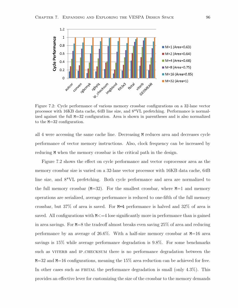
Chapter 7. Expanding and Exploring the VESPA Design Space 96
0
0.2
0.4
0.6
0.8
1
1.2
Cycle Performance
M=1 (Area=0.63)
M=2 (Area=0.64)
M=4 (Area=0.68)
M=8 (Area=0.75)
M=16 (Area=0.85)
M=32 (Area=1)
Figure 7.2: Cycle performance of various memory crossbar configurations on a 32-lane vectorprocessor with 16KB data cache, 64B line size, and 8*VL prefetching. Performance is normal-ized against the full M=32 configuration. Area is shown in parentheses and is also normalizedto the M=32 configuration.
all 4 were accessing the same cache line. Decreasing M reduces area and decreases cycle
performance of vector memory instructions. Also, clock frequency can be increased by
reducing M when the memory crossbar is the critical path in the design.
Figure 7.2 shows the effect on cycle performance and vector coprocessor area as the
memory crossbar size is varied on a 32-lane vector processor with 16KB data cache, 64B
line size, and 8*VL prefetching. Both cycle performance and area are normalized to
the full memory crossbar (M=32). For the smallest crossbar, where M=1 and memory
operations are serialized, average performance is reduced to one-fifth of the full memory
crossbar, but 37% of area is saved. For M=4 performance is halved and 32% of area is
saved. All configurations with M<=4 lose significantly more in performance than is gained
in area savings. For M=8 the tradeoff almost breaks even saving 25% of area and reducing
performance by an average of 26.6%. With a half-size memory crossbar at M=16 area
savings is 15% while average performance degradation is 9.8%. For some benchmarks
such as viterb and ip checksum there is no performance degradation between the
M=32 and M=16 configurations, meaning the 15% area reduction can be achieved for free.
In other cases such as fbital the performance degradation is small (only 4.3%). This
provides an effective lever for customizing the size of the crossbar to the memory demands

Chapter 7. Expanding and Exploring the VESPA Design Space 97
M=8
M=16
M=32
M=4
M=8
M=16
M=4
M=8
1
2
4
8192 16384 32768 65536
Normalized Cycle Count
Area
32 Lanes
16 Lanes
8 Lanes
Figure 7.3: Average normalized cycle count versus area for various memory crossbar config-urations on various numbers of lanes. All VESPA configuration have 16KB data cache, 64Bline size, and 8*VL prefetching. Cycles are normalized against the full M=32 configuration ona 32-lane VESPA.
of the application, however it can also be used to mitigate clock frequency degradation
caused by the large crossbars.
Figure 7.3 highlights the area/speed tradeoff possible using the memory crossbar
reduction. The figure shows the average cycle count of an 8, 16, and 32 lane VESPA each
with full, half, and quarter-sized memory crossbars all normalized to the 32-lane VESPA
with full memory crossbar. The 16-lane VESPA with M=8 is a half-sized memory crossbar
providing a useful area/performance design point between the full memory crossbar 8-
lane VESPA and the full 16-lane VESPA. Similarly the half-sized crossbar for 32 lanes
provides a mid-point between the full memory crossbars of the 16 and 32-lane VESPA
configurations. The quarter-sized crossbar with M=4 and 16 lanes performs worse and is
larger than the 8-lane full memory crossbar. In general, half-sized memory crossbars are
useful design points, while the quarter-sized memory crossbars are dominated by the full
crossbars with half as many lanes.
Figure 7.4 shows the effect on wall clock performance and clock frequency across all
values of M (normalized to M=32) on a 32-lane VESPA with 16KB data cache, 64B line
size, and 8*VL prefetching. For such a large vector processor, the many lanes and the
full crossbar limits clock frequency to 98 MHz compared to the 131 MHz achievable on

Chapter 7. Expanding and Exploring the VESPA Design Space 98
0
0.2
0.4
0.6
0.8
1
1.2
Wall Clock Performance
M=1 (clk=1.14)
M=2 (clk=1.1)
M=4 (clk=1.1)
M=8 (clk=1.06)
M=16 (clk=1.04)
M=32 (clk=1)
Figure 7.4: Wall clock performance of various memory crossbar configurations on a 32-lanevector processor with 16KB data cache, 64B line size, and 8*VL prefetching. Performance isnormalized against the full M=32 configuration. Clock frequency is shown in parentheses andis also normalized to the M=32 configuration.
a 1-lane VESPA. Reducing the memory crossbar to M=1 raises the clock frequency to
110 MHz but still leaves overall wall clock time at one-fifth the performance of the full
memory crossbar. In the cases where no cycle degradation was observed such as M=16
for viterb and ip checksum, the wall clock performance is actually better than the
full memory crossbar because of the 4% gain in clock frequency. In fbital the clock
frequency gain makes M=16 and M=32 equal in wall clock performance and hence allows
a free 15% area savings. This clock frequency improvement phenomenon occurs because
the memory crossbar is the critical path of the design. For configurations with fewer
lanes, or for a more highly-pipelined and highly-optimized design we would expect clock
frequency to remain relatively constant.
7.2 Vector Chaining in VESPA
Our goal of scaling soft processor performance is largely met by instantiating multiple
vector lanes using a soft vector processor. However, additional performance can be gained
by leveraging a key feature of traditional vector processors: the ability to concurrently
execute multiple vector instructions via vector chaining, as discussed in Chapter 2, Sec-
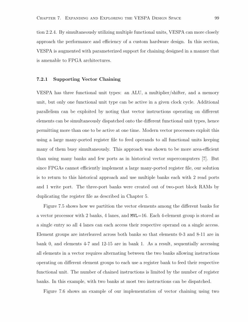
Chapter 7. Expanding and Exploring the VESPA Design Space 99
tion 2.2.4. By simultaneously utilizing multiple functional units, VESPA can more closely
approach the performance and efficiency of a custom hardware design. In this section,
VESPA is augmented with parameterized support for chaining designed in a manner that
is amenable to FPGA architectures.
7.2.1 Supporting Vector Chaining
VESPA has three functional unit types: an ALU, a multiplier/shifter, and a memory
unit, but only one functional unit type can be active in a given clock cycle. Additional
parallelism can be exploited by noting that vector instructions operating on different
elements can be simultaneously dispatched onto the different functional unit types, hence
permitting more than one to be active at one time. Modern vector processors exploit this
using a large many-ported register file to feed operands to all functional units keeping
many of them busy simultaneously. This approach was shown to be more area-efficient
than using many banks and few ports as in historical vector supercomputers [7]. But
since FPGAs cannot efficiently implement a large many-ported register file, our solution
is to return to this historical approach and use multiple banks each with 2 read ports
and 1 write port. The three-port banks were created out of two-port block RAMs by
duplicating the register file as described in Chapter 5.
Figure 7.5 shows how we partition the vector elements among the different banks for
a vector processor with 2 banks, 4 lanes, and MVL=16. Each 4-element group is stored as
a single entry so all 4 lanes can each access their respective operand on a single access.
Element groups are interleaved across both banks so that elements 0-3 and 8-11 are in
bank 0, and elements 4-7 and 12-15 are in bank 1. As a result, sequentially accessing
all elements in a vector requires alternating between the two banks allowing instructions
operating on different element groups to each use a register bank to feed their respective
functional unit. The number of chained instructions is limited by the number of register
banks. In this example, with two banks at most two instructions can be dispatched.
Figure 7.6 shows an example of our implementation of vector chaining using two

Chapter 7. Expanding and Exploring the VESPA Design Space 100
15141312
111098
3210
7654
Bank1
Bank0
vr0vr1
15141312
111098
3210
7654
vr31
15141312
111098
3210
7654
…
…
Figure 7.5: Element-partitioned vector register file banks shown for 2 banks, 4 lanes, andmaximum vector length 16. Note that accessing all elements in a vector requires oscillatingbetween both banks.
Bank 0(even
elments) Mult/Shift
MemUnit
ALU
Bank 1(odd
elments)
MUX
MUX
MUX
MUXM
UX
MUX
InstrBank Queue
VectorRegister
File
Figure 7.6: Vector chaining support for a 1-lane VESPA processor with 2 banks.
register banks to support a maximum of 2 vector instructions in flight for a 1-lane VESPA
processor. Once resource, read-after-write, and bank conflicts are resolved, instructions
will enter the Bank Queue and cycle between the even and odd element banks until
all element operations are completed. During that time another instruction can enter
the queue and rotate through the cyclical Bank Queue resulting in 2 element operations
being issued per cycle. As each operation completes the result is written back to the
appropriate register bank. Using a cyclical queue simplifies the control logic necessary
for assigning a bank to an element operation, but causes one or more cycle delays for the
few vector instructions which cannot start on an even element (most vector instructions

Chapter 7. Expanding and Exploring the VESPA Design Space 101
start with element 0).
The number of register banks, B, used to support vector chaining is parameterized and
must be a power of two. A value of 1 reduces VESPA to a single-issue vector processor
without vector chaining support eliminating the Bank Queue and associated multiplexing
illustrated in Figure 7.6. VESPA can potentially issue as many as B instructions at one
time, provided they each have available functional units. To increase the likelihood of
this, VESPA allows replication of the ALU for each bank, the APB parameter enables or
disables this feature. For example, with two banks and APB enabled, each vector lane
will have one ALU for each bank and in total two ALUs. Since multipliers are generally
scarce we do not support duplication for the multiply/shift unit, and we also do not
support multiple memory requests in-flight because of the system’s locking cache.
7.2.2 Impact of Vector Chaining
We measured the effect of the vector chaining implementation described above across our
benchmarks using an 8-lane vector processor with full memory support (16KB data cache,
64B cache line, and prefetching of 8*VL) implemented on the DE3 platform. We vary
the number of banks from 2 to 4 and for each toggle the ALU per bank APB parameter
and compare the resultant four designs to an analogous VESPA configuration without
vector chaining.
Figure 7.7 shows the cycle speedup of chaining across our benchmarks as well as the
area normalized to the 1 bank configuration. The area cost of banking is considerable,
starting at 27% for the second register bank and the expensive multiplexing logic needed
between the two banks. The average performance improvement of this 27% area invest-
ment is approximately 26%, and in the best case is 54%. Note that if instead of adding
a second bank, the designer opted to double the number of lanes to 16, the average
performance gain would be 49% for an area cost of 77%. Two banks provide half that
performance improvement at one third the area, and is hence a more fine-grain trade-off
than increasing lanes.
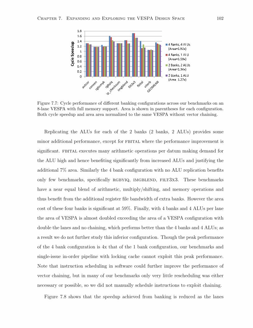
Chapter 7. Expanding and Exploring the VESPA Design Space 102
0
0.2
0.4
0.6
0.8
1
1.2
1.4
1.6
1.8
Cycle Speedup
4 Banks, 4 ALUs
(Area=1.92x)
4 Banks, 1 ALU
(Area=1.59x)
2 Banks, 2 ALUs
(Area=1.34x)
2 Banks, 1 ALU
(Area=1.27x)
Figure 7.7: Cycle performance of different banking configurations across our benchmarks on an8-lane VESPA with full memory support. Area is shown in parentheses for each configuration.Both cycle speedup and area area normalized to the same VESPA without vector chaining.
Replicating the ALUs for each of the 2 banks (2 banks, 2 ALUs) provides some
minor additional performance, except for fbital where the performance improvement is
significant. fbital executes many arithmetic operations per datum making demand for
the ALU high and hence benefiting significantly from increased ALUs and justifying the
additional 7% area. Similarly the 4 bank configuration with no ALU replication benefits
only few benchmarks, specifically rgbyiq, imgblend, filt3x3. These benchmarks
have a near equal blend of arithmetic, multiply/shifting, and memory operations and
thus benefit from the additional register file bandwidth of extra banks. However the area
cost of these four banks is significant at 59%. Finally, with 4 banks and 4 ALUs per lane
the area of VESPA is almost doubled exceeding the area of a VESPA configuration with
double the lanes and no chaining, which performs better than the 4 banks and 4 ALUs; as
a result we do not further study this inferior configuration. Though the peak performance
of the 4 bank configuration is 4x that of the 1 bank configuration, our benchmarks and
single-issue in-order pipeline with locking cache cannot exploit this peak performance.
Note that instruction scheduling in software could further improve the performance of
vector chaining, but in many of our benchmarks only very little rescheduling was either
necessary or possible, so we did not manually schedule instructions to exploit chaining.
Figure 7.8 shows that the speedup achieved from banking is reduced as the lanes
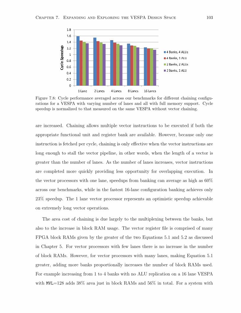
Chapter 7. Expanding and Exploring the VESPA Design Space 103
0
0.2
0.4
0.6
0.8
1
1.2
1.4
1.6
1.8
1 Lane 2 Lanes 4 Lanes 8 Lanes 16 Lanes
Cycle Speedup
4 Banks, 4 ALUs
4 Banks, 1 ALU
2 Banks, 2 ALUs
2 Banks, 1 ALU
Figure 7.8: Cycle performance averaged across our benchmarks for different chaining configu-rations for a VESPA with varying number of lanes and all with full memory support. Cyclespeedup is normalized to that measured on the same VESPA without vector chaining.
are increased. Chaining allows multiple vector instructions to be executed if both the
appropriate functional unit and register bank are available. However, because only one
instruction is fetched per cycle, chaining is only effective when the vector instructions are
long enough to stall the vector pipeline, in other words, when the length of a vector is
greater than the number of lanes. As the number of lanes increases, vector instructions
are completed more quickly providing less opportunity for overlapping execution. In
the vector processors with one lane, speedups from banking can average as high as 60%
across our benchmarks, while in the fastest 16-lane configuration banking achieves only
23% speedup. The 1 lane vector processor represents an optimistic speedup achievable
on extremely long vector operations.
The area cost of chaining is due largely to the multiplexing between the banks, but
also to the increase in block RAM usage. The vector register file is comprised of many
FPGA block RAMs given by the greater of the two Equations 5.1 and 5.2 as discussed
in Chapter 5. For vector processors with few lanes there is no increase in the number
of block RAMs. However, for vector processors with many lanes, making Equation 5.1
greater, adding more banks proportionally increases the number of block RAMs used.
For example increasing from 1 to 4 banks with no ALU replication on a 16 lane VESPA
with MVL=128 adds 38% area just in block RAMs and 56% in total. For a system with
Chapter 7. Expanding and Exploring the VESPA Design Space 104
1 Lane
2 Lanes
4 Lanes
8 Lanes
16 Lanes
0.0625
0.125
0.25
0.5
1
1 2 4 8
Wall Clock TIme
Area
2 Banks, 2 ALUs
2 Banks, 1 ALU
1 Bank, 1 ALU
Figure 7.9: Performance/area space of 1-16 lane vector processors with no chaining (1 bankwith 1 ALU), and 2-way chaining (2 banks with 1 ALU and 2 banks with 2 ALUs). Area andperformance are normalized to the 1 lane, 1 bank, 1 ALU configuration.
many unused block RAMs this increase can be justified even though only a fraction of
the capacity of each block RAM may be used. In fact, the unused capacity of the block
RAMs can be fully utilized by the vector processor with a corresponding increase in MVL
as seen in Equation 5.2.
Figure 7.9 shows the wall clock time versus area space of the no chaining configurations
from 1 to 16 lanes (depicted with solid diamonds). We overlay two vector chaining
configurations on the same figure and observe that the points with 2 banks and no ALU
replication appear about one third of the way to the next solid diamond, illustrating that
chaining can trade area/performance at finer increments than doubling the number of
lanes. Adding ALU replication slightly increases the performance and area of the soft
vector processor. Note that the 4-bank configurations are omitted since the area cost is
significant and the additional performance is often modest compared to 2 banks. Since
we have complete measurement capabilities of the area and performance we are able to
identify that vector chaining in an FPGA context is indeed a trade-off and not a global
improvement (it did not move VESPA toward the origin of the figure).
Chapter 7. Expanding and Exploring the VESPA Design Space 105
7.2.3 Vector Lanes and Powers of Two
Another option for fine-grain area/performance trade-offs is to use lane configurations
that are not powers of two, resulting in cumbersome control logic which involves multi-
plication and division operations. For example the vext.sv instruction extracts a single
element given by its index value in the vector. If a 9-lane vector configuration is used,
determining the element group to load from the register file would require dividing the
index by 9. By using a power of two this operation reduces to shifting by a constant,
which is free in hardware. Since this extra logic can impact clock frequency, and the
additional area overhead can be significant, this approach would generate inferior config-
urations that, in terms of Figure 7.9, would form a curve further from the origin than the
processors with lanes that are powers of two. Chaining, on the other hand, is shown to
directly compete with these configurations, and in Section 7.3 is shown to even improve
performance per unit area.
7.3 Exploring the VESPA Design Space
Using VESPA we have shown soft vector processors can scale performance while providing
several architectural parameters for fine-tuning and customization. This customization
is especially compelling in an FPGA context where designers can easily implement an
application-specific configuration. In this section we explore this design space more fully
by measuring the area and performance of hundreds of VESPA processors generated by
varying almost all VESPA parameters and implementing each configuration on the DE3
platform.
7.3.1 Selecting and Pruning the Design Space
Our aim is to derive a design space that captures many interesting tradeoffs without
an overwhelming number of design points. Each design point must be synthesized nine
times (once for implementing on the DE3, and 8 times across different seeds to average
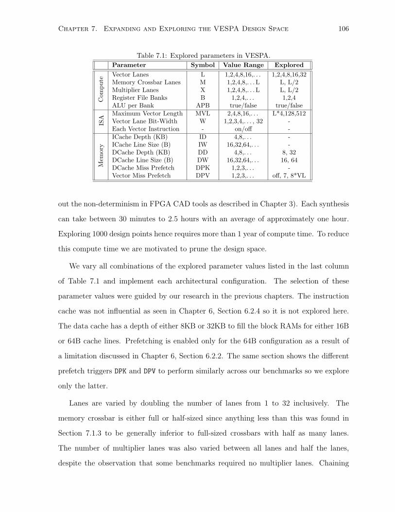
Chapter 7. Expanding and Exploring the VESPA Design Space 106
Table 7.1: Explored parameters in VESPA.Parameter Symbol Value Range Explored
Com
pute
Vector Lanes L 1,2,4,8,16,. . . 1,2,4,8,16,32Memory Crossbar Lanes M 1,2,4,8,. . . L L, L/2Multiplier Lanes X 1,2,4,8,. . . L L, L/2Register File Banks B 1,2,4,. . . 1,2,4ALU per Bank APB true/false true/false
ISA
Maximum Vector Length MVL 2,4,8,16,. . . L*4,128,512Vector Lane Bit-Width W 1,2,3,4,. . . , 32 -Each Vector Instruction - on/off -
Mem
ory
ICache Depth (KB) ID 4,8,. . . -ICache Line Size (B) IW 16,32,64,. . . -DCache Depth (KB) DD 4,8,. . . 8, 32DCache Line Size (B) DW 16,32,64,. . . 16, 64DCache Miss Prefetch DPK 1,2,3,. . . -Vector Miss Prefetch DPV 1,2,3,. . . off, 7, 8*VL
out the non-determinism in FPGA CAD tools as described in Chapter 3). Each synthesis
can take between 30 minutes to 2.5 hours with an average of approximately one hour.
Exploring 1000 design points hence requires more than 1 year of compute time. To reduce
this compute time we are motivated to prune the design space.
We vary all combinations of the explored parameter values listed in the last column
of Table 7.1 and implement each architectural configuration. The selection of these
parameter values were guided by our research in the previous chapters. The instruction
cache was not influential as seen in Chapter 6, Section 6.2.4 so it is not explored here.
The data cache has a depth of either 8KB or 32KB to fill the block RAMs for either 16B
or 64B cache lines. Prefetching is enabled only for the 64B configuration as a result of
a limitation discussed in Chapter 6, Section 6.2.2. The same section shows the different
prefetch triggers DPK and DPV to perform similarly across our benchmarks so we explore
only the latter.
Lanes are varied by doubling the number of lanes from 1 to 32 inclusively. The
memory crossbar is either full or half-sized since anything less than this was found in
Section 7.1.3 to be generally inferior to full-sized crossbars with half as many lanes.
The number of multiplier lanes was also varied between all lanes and half the lanes,
despite the observation that some benchmarks required no multiplier lanes. Chaining
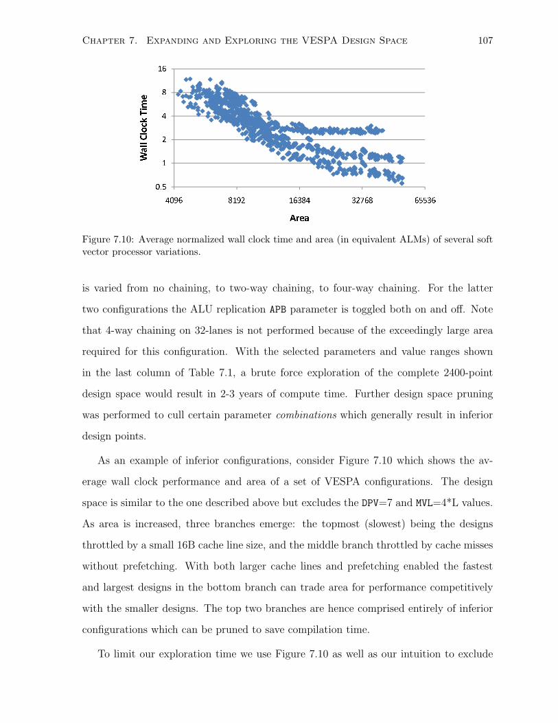
Chapter 7. Expanding and Exploring the VESPA Design Space 107
0.5
1
2
4
8
16
4096 8192 16384 32768 65536
Wall Clock Time
Area
Figure 7.10: Average normalized wall clock time and area (in equivalent ALMs) of several softvector processor variations.
is varied from no chaining, to two-way chaining, to four-way chaining. For the latter
two configurations the ALU replication APB parameter is toggled both on and off. Note
that 4-way chaining on 32-lanes is not performed because of the exceedingly large area
required for this configuration. With the selected parameters and value ranges shown
in the last column of Table 7.1, a brute force exploration of the complete 2400-point
design space would result in 2-3 years of compute time. Further design space pruning
was performed to cull certain parameter combinations which generally result in inferior
design points.
As an example of inferior configurations, consider Figure 7.10 which shows the av-
erage wall clock performance and area of a set of VESPA configurations. The design
space is similar to the one described above but excludes the DPV=7 and MVL=4*L values.
As area is increased, three branches emerge: the topmost (slowest) being the designs
throttled by a small 16B cache line size, and the middle branch throttled by cache misses
without prefetching. With both larger cache lines and prefetching enabled the fastest
and largest designs in the bottom branch can trade area for performance competitively
with the smaller designs. The top two branches are hence comprised entirely of inferior
configurations which can be pruned to save compilation time.
To limit our exploration time we use Figure 7.10 as well as our intuition to exclude
Chapter 7. Expanding and Exploring the VESPA Design Space 108
configurations with:
1. (L < 8) and (MVL = 512) – Configurations with few lanes can seldomly justify the
area for such large amount of vector state.
2. (L >= 8) and (DW = 16B) – Configurations with many lanes require wider cache
lines as seen in Figure 7.10.
3. (L >= 8) and (DPV = 0) – Configurations with many lanes require prefetching as
seen in Figure 7.10.
4. (DD = 8KB) and (DW = 64B) – Configurations which do not fully utilize their block
RAMs.
5. (DD = 32KB) and (DW = 16B) – Configurations with extra block RAMs used
only to expand the cache depth which was shown to be ineffective in accelerating
benchmark performance as seen in Section 6.2.1.
As a result of this pruning, the 2400 point design space resulting from all combina-
tions of parameter values in the last column of Table 7.1 is reduced to just 768 points.
With less than one-third the number of design points the exploration time is reduced
proportionately.
7.3.2 Exploring the Pruned Design Space
Our goal is to measure the area and performance of this 768-point design space and
confirm VESPA’s ability to: (i) span a very broad design space; and (ii) fill in this design
space allowing FPGA designers to choose an exact-fit configuration.
Figure 7.11 shows the vector coprocessor area and cycle count space of the 768 VESPA
configurations. The design space spans a total of 28x in area and 24x in performance
providing a huge range of design points for an FPGA embedded system designer to choose
from. Moreover, the data shows that VESPA provides fine-grain coverage of this design
space indeed allowing for precise selection of a configuration which closely matches the
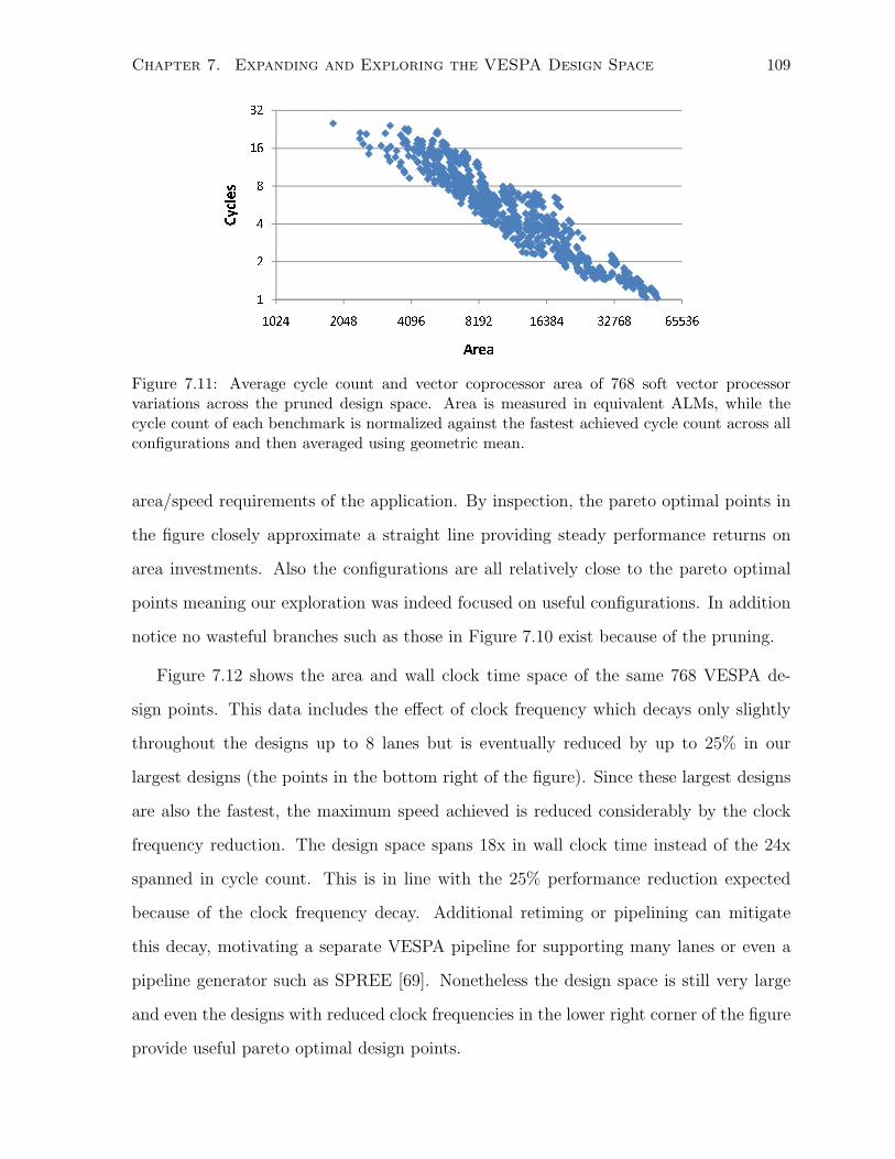
Chapter 7. Expanding and Exploring the VESPA Design Space 109
1
2
4
8
16
32
1024 2048 4096 8192 16384 32768 65536
Cycles
Area
Figure 7.11: Average cycle count and vector coprocessor area of 768 soft vector processorvariations across the pruned design space. Area is measured in equivalent ALMs, while thecycle count of each benchmark is normalized against the fastest achieved cycle count across allconfigurations and then averaged using geometric mean.
area/speed requirements of the application. By inspection, the pareto optimal points in
the figure closely approximate a straight line providing steady performance returns on
area investments. Also the configurations are all relatively close to the pareto optimal
points meaning our exploration was indeed focused on useful configurations. In addition
notice no wasteful branches such as those in Figure 7.10 exist because of the pruning.
Figure 7.12 shows the area and wall clock time space of the same 768 VESPA de-
sign points. This data includes the effect of clock frequency which decays only slightly
throughout the designs up to 8 lanes but is eventually reduced by up to 25% in our
largest designs (the points in the bottom right of the figure). Since these largest designs
are also the fastest, the maximum speed achieved is reduced considerably by the clock
frequency reduction. The design space spans 18x in wall clock time instead of the 24x
spanned in cycle count. This is in line with the 25% performance reduction expected
because of the clock frequency decay. Additional retiming or pipelining can mitigate
this decay, motivating a separate VESPA pipeline for supporting many lanes or even a
pipeline generator such as SPREE [69]. Nonetheless the design space is still very large
and even the designs with reduced clock frequencies in the lower right corner of the figure
provide useful pareto optimal design points.
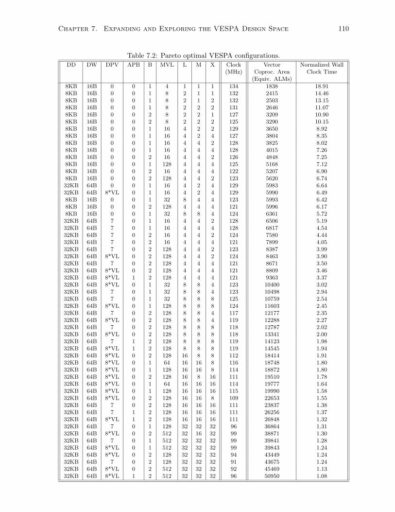
Chapter 7. Expanding and Exploring the VESPA Design Space 110
Table 7.2: Pareto optimal VESPA configurations.DD DW DPV APB B MVL L M X Clock Vector Normalized Wall
(MHz) Coproc. Area Clock Time(Equiv. ALMs)
8KB 16B 0 0 1 4 1 1 1 134 1838 18.918KB 16B 0 0 1 8 2 1 1 132 2415 14.468KB 16B 0 0 1 8 2 1 2 132 2503 13.158KB 16B 0 0 1 8 2 2 2 131 2646 11.078KB 16B 0 0 2 8 2 2 1 127 3209 10.908KB 16B 0 0 2 8 2 2 2 125 3290 10.158KB 16B 0 0 1 16 4 2 2 129 3650 8.928KB 16B 0 0 1 16 4 2 4 127 3804 8.358KB 16B 0 0 1 16 4 4 2 128 3825 8.028KB 16B 0 0 1 16 4 4 4 128 4015 7.268KB 16B 0 0 2 16 4 4 2 126 4848 7.258KB 16B 0 0 1 128 4 4 4 125 5168 7.128KB 16B 0 0 2 16 4 4 4 122 5207 6.908KB 16B 0 0 2 128 4 4 2 123 5620 6.7432KB 64B 0 0 1 16 4 2 4 129 5983 6.6432KB 64B 8*VL 0 1 16 4 2 4 129 5990 6.498KB 16B 0 0 1 32 8 4 4 123 5993 6.428KB 16B 0 0 2 128 4 4 4 121 5996 6.178KB 16B 0 0 1 32 8 8 4 124 6361 5.7232KB 64B 7 0 1 16 4 4 2 128 6506 5.1932KB 64B 7 0 1 16 4 4 4 128 6817 4.5432KB 64B 7 0 2 16 4 4 2 124 7580 4.4432KB 64B 7 0 2 16 4 4 4 121 7899 4.0532KB 64B 7 0 2 128 4 4 2 123 8387 3.9932KB 64B 8*VL 0 2 128 4 4 2 124 8463 3.9032KB 64B 7 0 2 128 4 4 4 121 8671 3.5032KB 64B 8*VL 0 2 128 4 4 4 121 8809 3.4632KB 64B 8*VL 1 2 128 4 4 4 121 9363 3.3732KB 64B 8*VL 0 1 32 8 8 4 123 10400 3.0232KB 64B 7 0 1 32 8 8 4 123 10498 2.9432KB 64B 7 0 1 32 8 8 8 125 10759 2.5432KB 64B 8*VL 0 1 128 8 8 8 124 11603 2.4532KB 64B 7 0 2 128 8 8 4 117 12177 2.3532KB 64B 8*VL 0 2 128 8 8 4 119 12288 2.2732KB 64B 7 0 2 128 8 8 8 118 12787 2.0232KB 64B 8*VL 0 2 128 8 8 8 118 13341 2.0032KB 64B 7 1 2 128 8 8 8 119 14123 1.9832KB 64B 8*VL 1 2 128 8 8 8 119 14545 1.9432KB 64B 8*VL 0 2 128 16 8 8 112 18414 1.9132KB 64B 8*VL 0 1 64 16 16 8 116 18748 1.8032KB 64B 8*VL 0 1 128 16 16 8 114 18872 1.8032KB 64B 8*VL 0 2 128 16 8 16 111 19510 1.7832KB 64B 8*VL 0 1 64 16 16 16 114 19777 1.6432KB 64B 8*VL 0 1 128 16 16 16 115 19990 1.5832KB 64B 8*VL 0 2 128 16 16 8 109 22653 1.5532KB 64B 7 0 2 128 16 16 16 111 23837 1.3832KB 64B 7 1 2 128 16 16 16 111 26256 1.3732KB 64B 8*VL 1 2 128 16 16 16 111 26848 1.3232KB 64B 7 0 1 128 32 32 32 96 36864 1.3132KB 64B 8*VL 0 2 512 32 16 32 99 38871 1.3032KB 64B 7 0 1 512 32 32 32 99 39841 1.2832KB 64B 8*VL 0 1 512 32 32 32 99 39843 1.2432KB 64B 8*VL 0 2 128 32 32 32 94 43449 1.2432KB 64B 7 0 2 128 32 32 32 91 43675 1.2432KB 64B 8*VL 0 2 512 32 32 32 92 45469 1.1332KB 64B 8*VL 1 2 512 32 32 32 96 50950 1.08

Chapter 7. Expanding and Exploring the VESPA Design Space 111
1
2
4
8
16
32
1024 2048 4096 8192 16384 32768 65536
Wall Clock Time
Area
Figure 7.12: Average wall clock time and vector coprocessor area of 768 soft vector processorvariations across the pruned design space. Area is measured in equivalent ALMs, while thewall clock time of each benchmark is normalized against the fastest achieved time across allconfigurations and then averaged using geometric mean.
Table 7.2 lists the pareto optimal VESPA configurations from the area/wall clock time
design space. These 56 configurations dominate the rest of the 712 designs meaning only
7.3% of the design space was useful. While this analysis is based on an average across
our benchmarks, on a per-application basis we expect a larger set of points to be useful.
The table is sorted starting from the smallest area design at the top, to the largest at
the bottom.
The smallest area design has 1 lane, 8KB data cache with 16B line size, MVL of 4,
and no chaining, prefetching or heterogeneous lanes. There are few neighbouring points
surrounding this configuration since most parameter values are not applicable or cause
large area investments. More small designs can be found in this region by including more
small MVL values in the exploration. As seen in Section 5.6 the MVL value can either
modestly or substantially affect the area for designs with few lanes. Had our search space
included a more fine-grain exploration of MVL values we would expect more neighbouring
points around this smallest area design—our current exploration has only one low value
of MVL (4*L) with the next smallest value being 128 which is very large for a one-lane
vector processor.
The pareto optimal configurations listed in the table highlight the contribution of
the VESPA parameters in creating useful designs. The full range of MVL values and

Chapter 7. Expanding and Exploring the VESPA Design Space 112
vector lanes are used, many of them with half-sized crossbars, or half as many lanes
with multipliers. All memory system configurations were used including all the prefetch-
ing strategies. Chaining varied between off and 2-way chaining through two banks—no
pareto optimal points were created using 4-way chaining. Finally the ALU replication
parameter, APB, was enabled for some of the designs with chaining. Overall we see that
the architectural parameters in VESPA each provide an effective means of trading area
for performance and each contribute towards selecting an efficient soft vector processor
configuration.
The clock frequency of each configuration is shown in the third-last column of the table
and quantifies the clock degradation previously discussed. The smallest configuration
achieves 134 MHz while the largest is reduced to 96 MHz. In general the clock frequency
is relatively stable across configurations with the same number of lanes. Despite the clock
degradation, increasing the number of lanes still provides ample performance acceleration.
7.3.3 Per-Application Analysis
A key motivation for FPGA-based soft processors is their ability to be customized to
a given application. This application-specific customization can aid FPGA designers in
meeting their system constraints. Since these constraints vary from system to system, in
the next two sections we examine the effect of two common cost functions: performance
and performance-per-area.
7.3.3.1 Fastest Per-Application Configurations
Across the complete 768-point design space the fastest overall processor is typically the
fastest for each benchmark. Most of VESPA’s parameters trade additional area for
increased performance, hence without an area constraint all benchmarks benefit from
adding more lanes, bigger caches, and more chaining. The prefetching strategy and MVL
value however can positively or negatively affect the performance for a given application.
Aside from these two parameter the other parameters can only increase performance
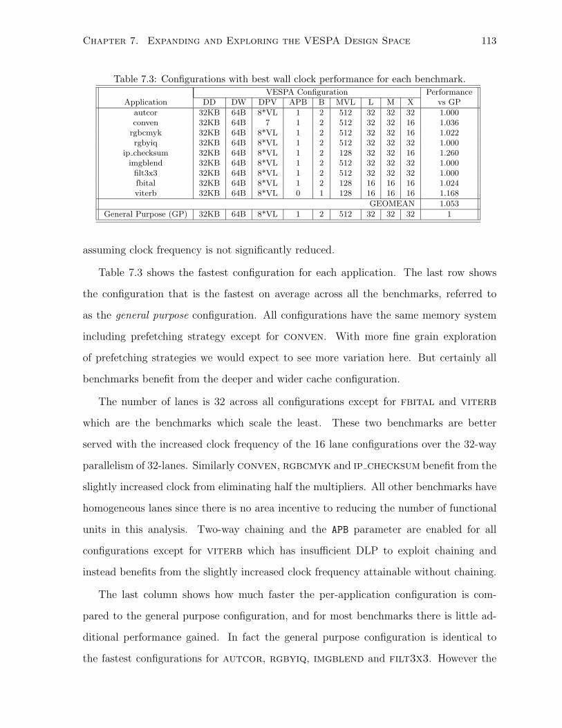
Chapter 7. Expanding and Exploring the VESPA Design Space 113
Table 7.3: Configurations with best wall clock performance for each benchmark.VESPA Configuration Performance
Application DD DW DPV APB B MVL L M X vs GP
autcor 32KB 64B 8*VL 1 2 512 32 32 32 1.000conven 32KB 64B 7 1 2 512 32 32 16 1.036
rgbcmyk 32KB 64B 8*VL 1 2 512 32 32 16 1.022rgbyiq 32KB 64B 8*VL 1 2 512 32 32 32 1.000
ip checksum 32KB 64B 8*VL 1 2 128 32 32 16 1.260imgblend 32KB 64B 8*VL 1 2 512 32 32 32 1.000filt3x3 32KB 64B 8*VL 1 2 512 32 32 32 1.000fbital 32KB 64B 8*VL 1 2 128 16 16 16 1.024viterb 32KB 64B 8*VL 0 1 128 16 16 16 1.168
GEOMEAN 1.053
General Purpose (GP) 32KB 64B 8*VL 1 2 512 32 32 32 1
assuming clock frequency is not significantly reduced.
Table 7.3 shows the fastest configuration for each application. The last row shows
the configuration that is the fastest on average across all the benchmarks, referred to
as the general purpose configuration. All configurations have the same memory system
including prefetching strategy except for conven. With more fine grain exploration
of prefetching strategies we would expect to see more variation here. But certainly all
benchmarks benefit from the deeper and wider cache configuration.
The number of lanes is 32 across all configurations except for fbital and viterb
which are the benchmarks which scale the least. These two benchmarks are better
served with the increased clock frequency of the 16 lane configurations over the 32-way
parallelism of 32-lanes. Similarly conven, rgbcmyk and ip checksum benefit from the
slightly increased clock from eliminating half the multipliers. All other benchmarks have
homogeneous lanes since there is no area incentive to reducing the number of functional
units in this analysis. Two-way chaining and the APB parameter are enabled for all
configurations except for viterb which has insufficient DLP to exploit chaining and
instead benefits from the slightly increased clock frequency attainable without chaining.
The last column shows how much faster the per-application configuration is com-
pared to the general purpose configuration, and for most benchmarks there is little ad-
ditional performance gained. In fact the general purpose configuration is identical to
the fastest configurations for autcor, rgbyiq, imgblend and filt3x3. However the

Chapter 7. Expanding and Exploring the VESPA Design Space 114
Table 7.4: Configurations with best performance-per-area for each benchmark.VESPA Configuration Performance per
Application DD DW DPV APB B MVL L M X Area vs GP
autcor 8KB 16B 0 0 2 128 8 8 8 1.068conven 32KB 64B 8*VL 0 2 128 8 8 4 1.054
rgbcmyk 32KB 64B 8*VL 0 1 64 16 16 8 1.071rgbyiq 32KB 64B 7 0 2 128 16 16 16 1.058
ip checksum 32KB 64B 7 0 2 32 8 8 4 1.087imgblend 32KB 64B 7 0 2 128 16 16 16 1.025filt3x3 32KB 64B 8*VL 0 4 512 16 16 16 1.070fbital 8KB 16B 0 0 1 32 8 4 8 1.246viterb 8KB 16B 0 1 2 4 1 1 1 1.356
GEOMEAN 1.110
General Purpose (GP) 32KB 64B 7 0 2 128 8 8 8 1
ip checksum benchmark is significantly faster with a smaller MVL value than the gen-
eral purpose configuration. A 26% speed improvement is seen as a result of the shorter
time required to sum all the elements in a vector. The viterb configuration gains 17%
performance due largely to clock frequency.
On average the fastest per-application configuration is 5.3% faster than the general
purpose configuration, but most of this is due to the large performance difference seen
with ip checksum and viterb. To better understand the efficiency gained by selecting
a processor on a per-application basis, one must consider the area costs in addition
to performance. Focussing only on performance acceleration leads to exorbitant area
investments for small performance improvements. In actual fact, other computations
could potentially use available FPGA area to more dramatically accelerate their execution
and better serve the complete system. We therefore seek configuration with the best
performance-per-area.
7.3.3.2 Best Performance-Per-Area Configurations
Performance-per-area is a commonly used metric for measuring efficiency which considers
both performance and area. To calculate performance-per-area we take the inverse of the
product between area and wall clock time, both measured as described in Chapter 3. The
measured area includes the complete processor system excluding the memory controller
and host communication hardware; the wall clock time is measured on the DE3 platform.
Chapter 7. Expanding and Exploring the VESPA Design Space 115
Table 7.4 shows the VESPA configuration with the best performance-per-area for each
benchmark selected out of the 768 explored designs. The last row shows the general pur-
pose configuration that achieves the best performance-per-area averaged arithmetically
across all benchmarks. The per-application configurations can achieve up to 35.6% (av-
erage of 11%) better performance-per-area over the general purpose configuration. The
selected configurations for each benchmark vary significantly from the general purpose
8-lane configuration with MVL=128, 2 banks, 32KB data cache, 64B line size, and 7 cache
line prefetching. Three of the benchmarks work best instead for the 8*VL prefetching
strategy, while another three select the smaller cache which does not support prefetching.
The number of lanes selected is typically 8 or 16 since 32-lane configurations require sig-
nificant area and also suffer from a significant clock frequency degradation. The viterb
benchmark being one of the least data-parallel applications benefits most from exploiting
a high degree of chaining on a 1-lane soft vector processor. This configuration is cer-
tainly the most interesting as it differs the most from the general purpose and improves
performance-per-area by 35.6%. The viterb configuration has 2 banks and is the only
one that benefits from enabling the APB parameter. The selected architecture is similar
to a scalar processor except the vector instructions are issued up to two per cycle across
the two ALUs, one multiplier, and the memory unit. Surprisingly, for this benchmark
this is more efficient in terms of performance-per-area than a 2-lane configuration.
The fbital benchmark achieves 24.6% better performance-per-area than the general
purpose configuration. This is gained largely by the half-sized crossbar and the reduced
vector state from the decreased MVL. Further area savings is gained by disabling chaining
in this configuration. The filt3x3 benchmark selects the largest configuration with 4
banks, MVL=512 and 16 homogeneous lanes achieving 7% improved performance-per-area
over the general purpose. The benchmarks with little or no multiply operations are seen
to employ heterogeneous lanes reducing the number of lanes with multipliers. This is
seen in conven, rgbcmyk, and ip checksum.
With the exception of viterb the benchmarks are characteristically similar: streaming-
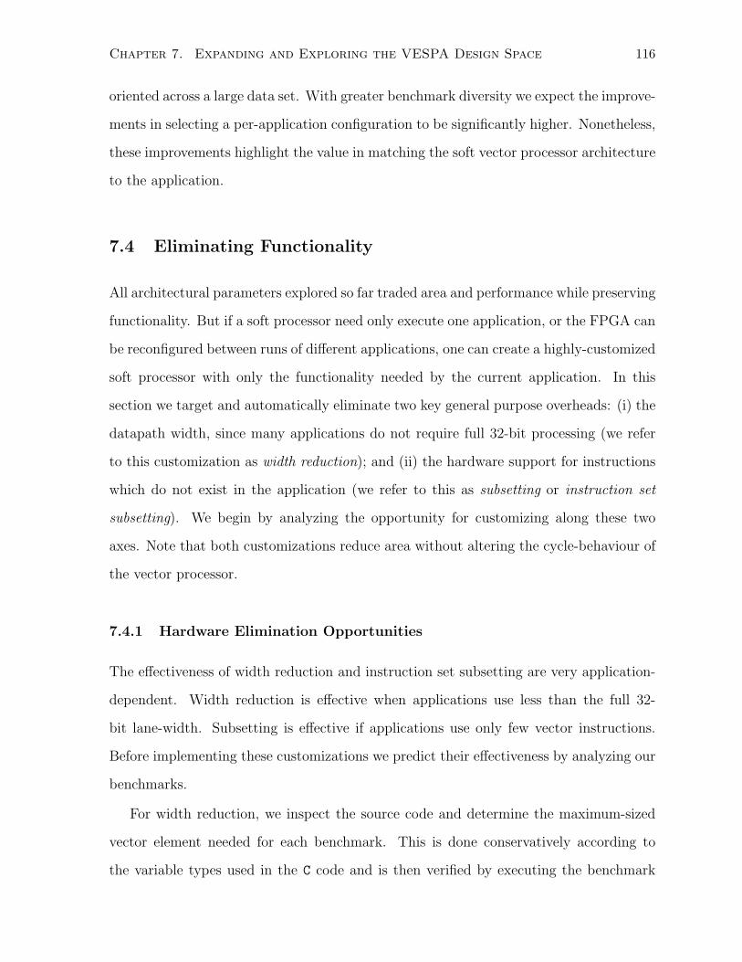
Chapter 7. Expanding and Exploring the VESPA Design Space 116
oriented across a large data set. With greater benchmark diversity we expect the improve-
ments in selecting a per-application configuration to be significantly higher. Nonetheless,
these improvements highlight the value in matching the soft vector processor architecture
to the application.
7.4 Eliminating Functionality
All architectural parameters explored so far traded area and performance while preserving
functionality. But if a soft processor need only execute one application, or the FPGA can
be reconfigured between runs of different applications, one can create a highly-customized
soft processor with only the functionality needed by the current application. In this
section we target and automatically eliminate two key general purpose overheads: (i) the
datapath width, since many applications do not require full 32-bit processing (we refer
to this customization as width reduction); and (ii) the hardware support for instructions
which do not exist in the application (we refer to this as subsetting or instruction set
subsetting). We begin by analyzing the opportunity for customizing along these two
axes. Note that both customizations reduce area without altering the cycle-behaviour of
the vector processor.
7.4.1 Hardware Elimination Opportunities
The effectiveness of width reduction and instruction set subsetting are very application-
dependent. Width reduction is effective when applications use less than the full 32-
bit lane-width. Subsetting is effective if applications use only few vector instructions.
Before implementing these customizations we predict their effectiveness by analyzing our
benchmarks.
For width reduction, we inspect the source code and determine the maximum-sized
vector element needed for each benchmark. This is done conservatively according to
the variable types used in the C code and is then verified by executing the benchmark
Chapter 7. Expanding and Exploring the VESPA Design Space 117
Table 7.5: Hardware elimination opportunites across all benchmarks.
Largest Data Percent of SupportedBenchmark Type Size VIRAM ISA usedautcor 32 bits 9.6%conven 1 bit 5.9%fbital 16 bits 14.1%viterb 16 bits 13.3%
rgbcmyk 8 bits 5.9%rgbyiq 16 bits 8.1%
ip checksum 32 bits 8.1%imgblend 8 bits 7.4%filt3x3 8 bits 7.4%
in hardware on a VESPA configuration with reduced width. More aggressive width
reduction can consider the data set and determine for example that despite using a 16-
bit data type, the application requires only 11 bits. The BitValue compiler is an example
of such a system [11]. In general we do not perform this aggressive customization except
for the case of conven which by inspection uses only 1-bit data elements and provides
a best-case width-reduction result.
Table 7.5 shows the largest data type size used by each benchmark in the middle col-
umn. All benchmarks except autcor and ip checksum use less than 32-bit data types
hence providing ample opportunity for width reduction in the vector lanes. Three of the
benchmarks, rgbcmyk, imgblend and filt3x3 use only 8-bit data types, while con-
ven uses only 1-bit binary values. These four benchmarks present the most opportunity
for area savings through width reduction.
Table 7.5 shows the percentage of the total supported vector instruction set used
by each benchmark. These values were determined by extracting the number of unique
vector instructions that exist in a binary and dividing by the total number of vector
instructions VESPA supports. Less than 10% of the vector instruction set is used in all
benchmarks except for fbital and viterb. For these two benchmarks 14.1% and 13.3%
of the vector instruction set is used respectively. With all benchmarks using less than
15%, the opportunity for subsetting appears promising. These usages may not correlate
Chapter 7. Expanding and Exploring the VESPA Design Space 118
with the area savings achieved through subsetting since eliminating instruction variants
may remove some multiplexer paths, but larger savings are achieved when whole func-
tional units are removed. Because of this, the specific instructions used by the application
can have a big impact on the area savings.
Overall, the values in the table motivate the pursuit of both of these customization
techniques. Note that no benchmark was modified to aid or exaggerate the impact of
these techniques. Certainly more aggressive customization can re-code benchmarks to
use reduced widths and fewer instruction types, but our results are based on unmodified
original versions of our benchmarks.
7.4.2 Impact of Vector Datapath Width Reduction (W)
The width of each lane can be modified by simply changing the W parameter in the VESPA
Verilog code which will automatically implement the corresponding width-reduced vector
coprocessor. Although a 1-bit datapath can, with some hardware overhead, continue to
support 32-bit values, VESPA does not insert this bit-serialization hardware overhead.
Therefore a soft vector processor with lane width W will only correctly execute benchmarks
if their computations do not exceed W bits. The area of a conventional hard vector
processor cannot be reduced once it is fabricated, so designers opt instead to dynamically
(with some area overhead) reclaim any unused vector lane datapath width to emulate an
increased number of lanes, hence gaining performance. Our current benchmarks typically
operate on a single data width, making support for dynamically configuring vector lane
width and number of lanes uninteresting—however for a different set of applications this
could be motivated.
Figure 7.13 shows the effect of width reduction on a 16-lane VESPA with full memory
crossbar and 16KB data cache with 64B cache line size. Starting from a 1-bit vector lane
width we double the width until reaching the full 32-bit configuration. The area is
reduced to almost one-quarter in the 1-bit configuration with further reduction limited
due to the control logic, vector state, and address generation which are unaffected by
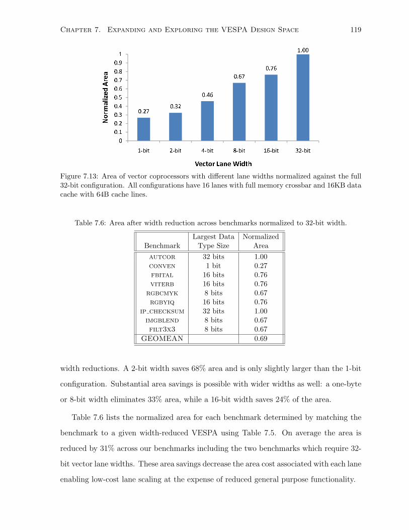
Chapter 7. Expanding and Exploring the VESPA Design Space 119
0.270.32
0.46
0.67
0.76
1.00
0
0.1
0.2
0.3
0.4
0.5
0.6
0.7
0.8
0.9
1
1-bit 2-bit 4-bit 8-bit 16-bit 32-bit
Normalized Area
Vector Lane Width
Figure 7.13: Area of vector coprocessors with different lane widths normalized against the full32-bit configuration. All configurations have 16 lanes with full memory crossbar and 16KB datacache with 64B cache lines.
Table 7.6: Area after width reduction across benchmarks normalized to 32-bit width.
Largest Data NormalizedBenchmark Type Size Areaautcor 32 bits 1.00conven 1 bit 0.27fbital 16 bits 0.76viterb 16 bits 0.76
rgbcmyk 8 bits 0.67rgbyiq 16 bits 0.76
ip checksum 32 bits 1.00imgblend 8 bits 0.67filt3x3 8 bits 0.67
GEOMEAN 0.69
width reductions. A 2-bit width saves 68% area and is only slightly larger than the 1-bit
configuration. Substantial area savings is possible with wider widths as well: a one-byte
or 8-bit width eliminates 33% area, while a 16-bit width saves 24% of the area.
Table 7.6 lists the normalized area for each benchmark determined by matching the
benchmark to a given width-reduced VESPA using Table 7.5. On average the area is
reduced by 31% across our benchmarks including the two benchmarks which require 32-
bit vector lane widths. These area savings decrease the area cost associated with each lane
enabling low-cost lane scaling at the expense of reduced general purpose functionality.
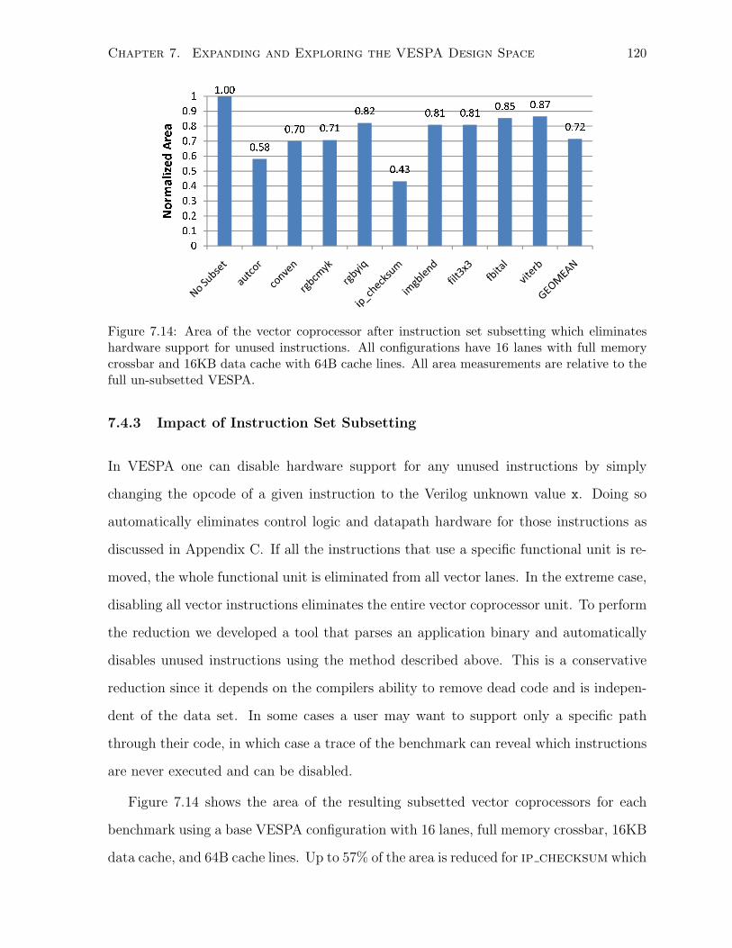
Chapter 7. Expanding and Exploring the VESPA Design Space 120
1.00
0.58
0.70 0.71
0.82
0.43
0.81 0.810.85 0.87
0.72
0
0.1
0.2
0.3
0.4
0.5
0.6
0.7
0.8
0.9
1
Normalized Area
Figure 7.14: Area of the vector coprocessor after instruction set subsetting which eliminateshardware support for unused instructions. All configurations have 16 lanes with full memorycrossbar and 16KB data cache with 64B cache lines. All area measurements are relative to thefull un-subsetted VESPA.
7.4.3 Impact of Instruction Set Subsetting
In VESPA one can disable hardware support for any unused instructions by simply
changing the opcode of a given instruction to the Verilog unknown value x. Doing so
automatically eliminates control logic and datapath hardware for those instructions as
discussed in Appendix C. If all the instructions that use a specific functional unit is re-
moved, the whole functional unit is eliminated from all vector lanes. In the extreme case,
disabling all vector instructions eliminates the entire vector coprocessor unit. To perform
the reduction we developed a tool that parses an application binary and automatically
disables unused instructions using the method described above. This is a conservative
reduction since it depends on the compilers ability to remove dead code and is indepen-
dent of the data set. In some cases a user may want to support only a specific path
through their code, in which case a trace of the benchmark can reveal which instructions
are never executed and can be disabled.
Figure 7.14 shows the area of the resulting subsetted vector coprocessors for each
benchmark using a base VESPA configuration with 16 lanes, full memory crossbar, 16KB
data cache, and 64B cache lines. Up to 57% of the area is reduced for ip checksum which
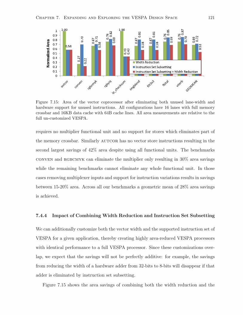
Chapter 7. Expanding and Exploring the VESPA Design Space 121
1.00
0.27
0.67 0
.76
1.00
0.67
0.67 0
.76
0.76
0.69
0.58
0.70
0.71 0
.82
0.43
0.81
0.81
0.85
0.87
0.72
0.22
0.58 0
.68
0.43
0.58
0.58 0
.69
0.70
0.53
0
0.1
0.2
0.3
0.4
0.5
0.6
0.7
0.8
0.9
1
Normalized Area
Width Reduction
Instruction Set Subsetting
Instruction Set Subsetting + Width Reduction
Figure 7.15: Area of the vector coprocessor after eliminating both unused lane-width andhardware support for unused instructions. All configurations have 16 lanes with full memorycrossbar and 16KB data cache with 64B cache lines. All area measurements are relative to thefull un-customized VESPA.
requires no multiplier functional unit and no support for stores which eliminates part of
the memory crossbar. Similarly autcor has no vector store instructions resulting in the
second largest savings of 42% area despite using all functional units. The benchmarks
conven and rgbcmyk can eliminate the multiplier only resulting in 30% area savings
while the remaining benchmarks cannot eliminate any whole functional unit. In those
cases removing multiplexer inputs and support for instruction variations results in savings
between 15-20% area. Across all our benchmarks a geometric mean of 28% area savings
is achieved.
7.4.4 Impact of Combining Width Reduction and Instruction Set Subsetting
We can additionally customize both the vector width and the supported instruction set of
VESPA for a given application, thereby creating highly area-reduced VESPA processors
with identical performance to a full VESPA processor. Since these customizations over-
lap, we expect that the savings will not be perfectly additive: for example, the savings
from reducing the width of a hardware adder from 32-bits to 8-bits will disappear if that
adder is eliminated by instruction set subsetting.
Figure 7.15 shows the area savings of combining both the width reduction and the
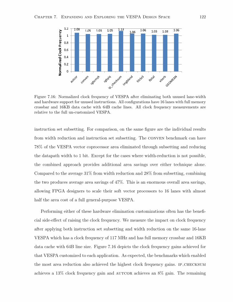
Chapter 7. Expanding and Exploring the VESPA Design Space 122
1.081.05 1.05 1.05 1.13
1.061.06
1.03 1.031.06
0
0.2
0.4
0.6
0.8
1
1.2
Normalized Clock Frequency
Figure 7.16: Normalized clock frequency of VESPA after eliminating both unused lane-widthand hardware support for unused instructions. All configurations have 16 lanes with full memorycrossbar and 16KB data cache with 64B cache lines. All clock frequency measurements arerelative to the full un-customized VESPA.
instruction set subsetting. For comparison, on the same figure are the individual results
from width reduction and instruction set subsetting. The conven benchmark can have
78% of the VESPA vector coprocessor area eliminated through subsetting and reducing
the datapath width to 1 bit. Except for the cases where width-reduction is not possible,
the combined approach provides additional area savings over either technique alone.
Compared to the average 31% from width reduction and 28% from subsetting, combining
the two produces average area savings of 47%. This is an enormous overall area savings,
allowing FPGA designers to scale their soft vector processors to 16 lanes with almost
half the area cost of a full general-purpose VESPA.
Performing either of these hardware elimination customizations often has the benefi-
cial side-effect of raising the clock frequency. We measure the impact on clock frequency
after applying both instruction set subsetting and width reduction on the same 16-lane
VESPA which has a clock frequency of 117 MHz and has full memory crossbar and 16KB
data cache with 64B line size. Figure 7.16 depicts the clock frequency gains achieved for
that VESPA customized to each application. As expected, the benchmarks which enabled
the most area reduction also achieved the highest clock frequency gains. ip checksum
achieves a 13% clock frequency gain and autcor achieves an 8% gain. The remaining

Chapter 7. Expanding and Exploring the VESPA Design Space 123
benchmarks experience between 3% and 6% clock frequency improvements for an overall
average of 6% faster clock than without subsetting and width reduction.
7.5 Summary
The reprogrammable fabric of FPGAs allows designers to choose an exact-fit processor
solution. In the case of soft vector processors the most powerful parameter is the number
of vector lanes which can be chosen depending on the amount of data level parallelism in
an application. But this decision can also be influenced by other architectural parameters
presented in this chapter which can change the area costs and speed improvements of
adding more lanes.
We implemented heterogeneous lanes allowing the designer to reduce the number of
lanes which support multiplication, as well as the number of lanes connected to the
memory crossbar. With this ability, a designer can conserve FPGA multiply-accumulate
blocks for applications with few multiplication and shift operations, and also reduce the
size of the memory crossbar for applications with low demand of the memory system.
An FPGA-specific implementation of chaining was added to VESPA without requiring
the large many-ported register files typically used. By interleaving across register file
banks chaining can dispatch as many instructions as there are banks. We scale the banks
up to 4 and observe significant performance improvements over no chaining. In addition
by replicating the ALU within each lane we increase the likelihood of dispatching multiple
vector instructions hence further increasing performance albeit at a substantial area cost.
The resulting design space of VESPA was explored after pruning it to 768 useful
design points. The design space spanned 28x in area and 24x in cycle count (18x in
wall clock time). Using VESPA’s many architectural parameters this broad space was
effectively filled in allowing precise selection of the desired area/performance. Also,
significant improvements were observed when selecting a per-application configuration
over the fastest or best performance-per-area over all our benchmarks, despite the similar
Chapter 7. Expanding and Exploring the VESPA Design Space 124
characteristics in these benchmarks.
Finally, we examined the area savings in removing unneeded datapath width for
benchmarks that do not require full 32-bit processing. Lanes were shrunk to as small
as 1-bit achieving a size almost one-fourth the original vector coprocessor area. We also
implemented and evaluated our infrastructure for automatically parsing an application
binary and removing all control and datapath hardware for vector instructions that do not
appear in the binary. In the best case this instruction set subsetting can eliminate more
than half the vector coprocessor area. Combining both techniques yields area savings as
high as 78% and on average 47%.

Chapter 8
Soft Vector Processors vs Manual
FPGA Hardware Design
The aim of this thesis is to enable easier creation of computation engines using software
development instead of through more difficult hardware design. This is done by offering
FPGA designers the option of scaling the performance of data parallel computations
using a soft vector processor. The previous chapter showed that a broad space of VESPA
configurations exists, but deciding on any of these configurations intelligently requires
analysis of the costs and benefits of using a soft vector processor instead of manually
designing FPGA hardware. While it is difficult to measure the ease of use benefit, it
is possible to quantify the concrete aspects of performance and area. In this chapter
we answer the question of how does the area and performance of a soft vector processor
compare to hardware? With this information an FPGA designer can more accurately
assess the costs and benefits of either implementation, including a scalar soft processor
implementation, and select the implementation that best meets the needs of the system.
Moreover, this data enables us to benchmark the progress of this research in having
vector-extended soft processors compete with manual hardware design.
Previous works [27, 58] studied the benefits of FPGA hardware versus hard proces-
sors without considering soft processors. Soft vector processors were compared against
125
Chapter 8. Soft Vector Processors vs Manual FPGA Hardware Design 126
automatically generated hardware from the Altera C2H behavioural synthesis tool and
found to achieve better scalability for 16-way parallelism and beyond [75]. Our compar-
ison differs by comparing soft vector processors to custom-made FPGA hardware which
is the most likely alternative to a soft processor implementation.
We compare the area and performance of the following three implementations of
our benchmarks created via different design entry methods: (i) out-of-the-box C code
executed on the MIPS-based SPREE scalar soft processor; (ii) hand-vectorized assembly
language executed on many variations of our VESPA soft vector processor; and (iii)
hardware designed manually in Verilog at the register transfer level. This comparison
was initially evaluated on the TM4 platform [73] but in this thesis we use the newer DE3
board. While our DE3-based infrastructure is well equipped for evaluating the first scalar
and vector processors, evaluating hardware requires manual design of hardware circuits
from a C benchmark. To design and evaluate such a circuit with the same realism used
to evaluate the processors would require many weeks or months for each benchmark. We
hence simplify the hardware design process as described in the next section.
8.1 Designing Custom Hardware Circuits
We created custom FPGA hardware by manually converting each benchmark into a
Verilog hardware circuit. Two factors heavily influence the implementation of this hard-
ware circuit: (i) the assumed system-level design constraints require certain levels of
performance as well as communication with specific peripherals; and (ii) the idealized
assumptions we made to simplify and reduce the design time for each hardware circuit.
Both of these are described below.
8.1.1 System-Level Design Constraints
For any given application, there are many hardware design variations ranging from area-
optimized 1-bit datapaths to extremely parallel high-performance implementations. In
Chapter 8. Soft Vector Processors vs Manual FPGA Hardware Design 127
this work we focus on performance and implement the latter. Similarly, the peripherals
used in the design will greatly influence its implementation. For example, a circuit
that receives its data from on-chip SRAM may be designed significantly different than
a circuit relying on serial RS-232 communication for its data. To fairly compare the
hardware circuits with the processor implementations, we use similar memories for the
data storage in both. Specifically we apply the following constraints on the hardware
system to match those in the processors:
1. Memory Width – There is only one 128-bit wide path to memory, hence we
assume a typical 64-pin (128 bits per clock) double data rate DRAM module.
2. Memory Usage – Input/output data starts/ends in memory. Internal storage can
be used for any partial or temporary results, but the final result must be written
to memory.
3. No Value Optimizations – All input data is assumed to be unknown at design-
time—i.e., we perform no value-specific or value-range-specific optimizations.
We expect that without these constraints, the performance of the hardware circuits
could be increased more than that of the processors. However to experimentally eval-
uate this would require re-engineering of the SPREE and VESPA soft processors and
modification of the benchmarks. To avoid this added effort we apply these constraints
to the hardware and as a result constrain the hardware design with conservative design
assumptions.
8.1.2 Simplifying Hardware Design Optimistically
The design of custom FPGA hardware requires months of effort to plan, implement, and
verify. Indeed, the complications associated with this effort motivate the introduction
of soft vector processors to reduce the amount of hardware design required in a digital
system. Rather than embracing these complications and pursuing full and complete hard-

Chapter 8. Soft Vector Processors vs Manual FPGA Hardware Design 128
ware implementations for each benchmark, we make the following optimistic assumptions
to make this comparison measurement tractable in the time available.
1. Benchmark Selection – Hardware implementations were designed for six out of
the nine benchmarks—fbital, viterb, and filt3x3 were excluded because of
their relative complexity which would have resulted in extremely difficult hardware
implementations. The six remaining benchmarks are very streaming-oriented re-
sulting in simpler datapath designs. A key side-effect of this simplification is that
these benchmarks can readily take advantage of parallel hardware circuits. This
makes the simplification optimistic for the hardware since benchmarks with more
complicated control would perform more similar to a processor.
2. Datapath Only – Any control logic or hardware for sending requests to/from the
memory controller is assumed to have negligible size and ideal performance in both
clock frequency and cycle count. In other words, only the datapath of the circuits
are designed assuming input and output data streams are already entering and
exiting the circuit. This assumption is optimistic in general but more reasonable
for our benchmarks which access mostly contiguous arrays which can be tracked
with a single counter and streamed at the highest memory bandwidth.
3. No Datapath Stalls – The datapath is fully pipelined, requires no stalls, and
assumes a continuous flow of data, and hence does not implement stalling/buffering
logic needed to handle data flow interruptions caused by DRAM refreshing for
example. This is also optimistic but in the context of our streaming benchmarks
with very predictable memory accesses, many data stalls can be avoided or hidden.
4. Memory Alignment – Data is assumed to be aligned in memory to the near-
est 128-bit boundary, eliminating the need for shifting and alignment logic. This
provides a significant area advantage for some benchmarks which would otherwise
require a memory crossbar similar to that in VESPA.
Chapter 8. Soft Vector Processors vs Manual FPGA Hardware Design 129
5. Memory Speed – We do not let the speed of the memory limit the performance of
the hardware circuits. In other words, we allow the 128-bit words to be transmitted
at the full clock rate of the hardware circuit despite the fact that this clock rate is
faster than the DDR2 DIMM used on the DE3 platform for the soft processors.
In summary, we build only the datapath of the circuit for the most streaming-oriented
benchmarks under optimistic assumptions about the control logic and transfer of data.
The memory being modelled is effectively an on-chip memory with a single 128-bit wide
port. This assumption is a valid approximation since the latency of an off-chip mem-
ory could be amortized over the large contiguous access patterns in the benchmarks.
Nonetheless, our idealizations imply that 100% of the memory bandwidth is utilized
by the hardware circuit, while our consultations with industry revealed that typical
FPGA system designers have difficulty achieving 50% utilization [9]. Hence, our sim-
ple benchmarks and simplifying assumptions have significantly idealized our hardware
results meaning this study can be interpreted as an upper-bound on the advantages of
custom hardware circuits.
As an example, consider the ip checksum benchmark which simply sums all the
16-bit elements in an array. The hardware circuit used to implement this benchmark is
shown in Figure 8.1. Since the array is stored contiguously in memory we can assume
8 16-bit words arrive from the 128-bit memory every clock cycle. Because addition is
commutative we can separately accumulate the 8 words each in their own register. After
the entire array has been processed we can reduce the 8 sums via an adder tree into a
single 32-bit scalar sum. The circuit shown is easy to build since it neglects the cycle-
to-cycle behaviour of control logic and data arrival, yet it captures the most significant
part of the overall area.
Although not quantified, we can qualitatively discuss the components missing from
the circuit and approximate their contribution to overall area. Missing from the figure is
a counter which stores and increments the address currently being accessed in the array.
Similarly absent is another counter for tracking the total progress and signalling when
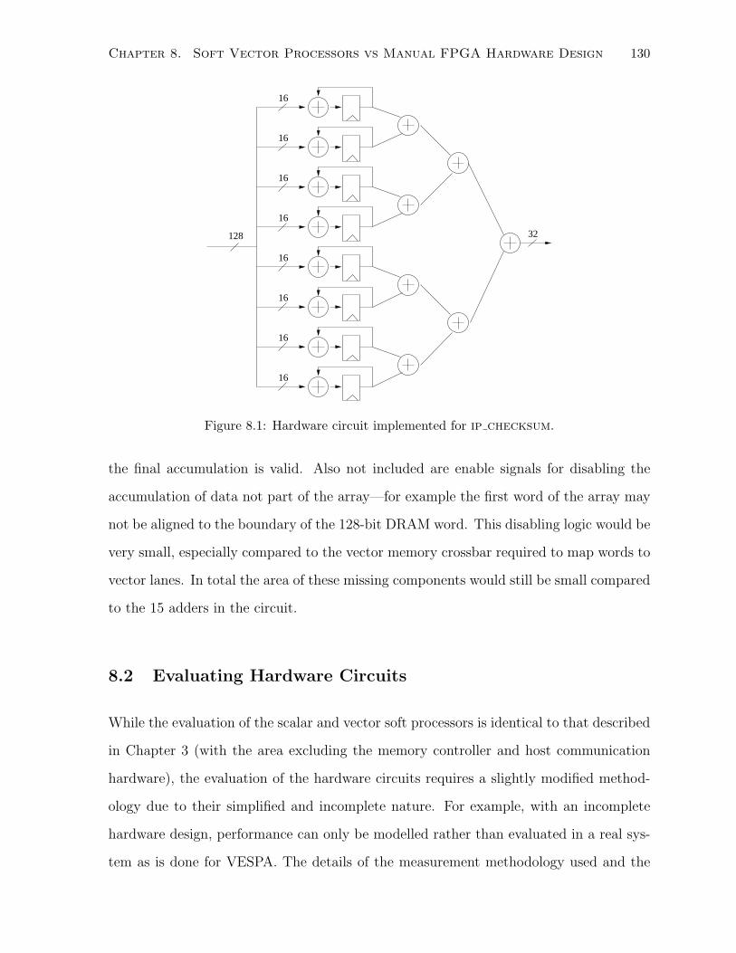
Chapter 8. Soft Vector Processors vs Manual FPGA Hardware Design 130
16
16
16
16
16
16
16
16
128 32
Figure 8.1: Hardware circuit implemented for ip checksum.
the final accumulation is valid. Also not included are enable signals for disabling the
accumulation of data not part of the array—for example the first word of the array may
not be aligned to the boundary of the 128-bit DRAM word. This disabling logic would be
very small, especially compared to the vector memory crossbar required to map words to
vector lanes. In total the area of these missing components would still be small compared
to the 15 adders in the circuit.
8.2 Evaluating Hardware Circuits
While the evaluation of the scalar and vector soft processors is identical to that described
in Chapter 3 (with the area excluding the memory controller and host communication
hardware), the evaluation of the hardware circuits requires a slightly modified method-
ology due to their simplified and incomplete nature. For example, with an incomplete
hardware design, performance can only be modelled rather than evaluated in a real sys-
tem as is done for VESPA. The details of the measurement methodology used and the

Chapter 8. Soft Vector Processors vs Manual FPGA Hardware Design 131
performance modelling are discussed below.
8.2.1 Area Measurement
The hardware circuits are synthesized for the Stratix III FPGA on our DE3 platform
using the same method for measuring actual silicon area of the design in equivalent ALMs
as discussed in Chapter 3. Only the datapath is synthesized assuming, as mentioned
previously, that control logic and memory request logic for communicating with the
memory can be implemented with negligible area.
8.2.2 Clock Frequency Measurement
The clock frequency of the hardware circuits is measured through a full synthesis onto
the FPGA over multiple seeds in the manner described in Chapter 3.
8.2.3 Cycle Count Measurement
Cycle count performance is modelled by considering the transfer of the data set through
the pipelined datapath, which performs the computation as the data flows through the
pipeline. As previously mentioned it is assumed that 128 bits are transfered on every
clock cycle at the clock speed of the hardware circuit which is faster than the DIMM
on the DE3. Therefore, to transfer the 40960 bytes of input data for the ip checksum
benchmark requires 2560 clock cycles. Then, to transfer the 40 bytes of output data
requires 3 cycles. The 4-cycle latency through the pipeline is also added to the cycle count
yielding a total of 2560 + 3 + 4 = 2567 clock cycles for the ip checksum benchmark.
In general the equation for calculating cycle performance of a streaming benchmark is
given by
Ncycles = InputBytes/16 + OutputBytes/16 + pipeline latency (8.1)
where InputBytes are the number of bytes in the input data set, OutputBytes are the
number of bytes in the output data set, and pipeline latency is the number of stages in

Chapter 8. Soft Vector Processors vs Manual FPGA Hardware Design 132
the pipeline. All computations are performed in a pipelined fashion in parallel with the
transfer of data, which is measured in the first two terms in the equation. For example,
the circuit for ip checksum is computing the checksum across some data values at the
same time that later data is being fetched into the datapath. As discussed earlier, we
assume memory latency can be hidden because of the sequential memory accesses in our
benchmarks. As a consequence, this makes our results equivalent to being executed using
128-bit wide on-chip block RAMs for memory.
8.2.4 Area-Delay Product
For a given digital system, there may be a heavier emphasis on area than performance, or
vice-versa. However, it is important to have an understanding of the overall performance-
per-area of candidate designs motivating us to measure area-delay product as is tradition-
ally done for digital circuits. We use the silicon area measured in equivalent ALMs for
area and the wall-clock-time of benchmark execution as the delay. The wall-clock-time
is measured by multiplying the cycle counts with the minimum clock period reported by
the CAD tools.
8.3 Implementing Hardware Circuits
The six selected benchmarks were implemented in Verilog under the constraints and
optimistic simplifications discussed earlier. Each circuit was tested in simulation using
test vectors to ensure the correct compute elements exist in the datapath.
Table 8.1 lists the FPGA resources used, clock rates, and cycle counts for each bench-
mark circuit. The number of ALMs is relatively small compared to VESPA, especially for
conven and ip checksum. Some of this is due to our assumptions about the negligible
area consumed by control logic and memory request logic.
The table also shows the extraordinarily high clock frequencies achieved by the hard-
ware circuits. Clock rates range between 274-476 MHz, all faster than the 266 MHz of

Chapter 8. Soft Vector Processors vs Manual FPGA Hardware Design 133
Table 8.1: Hardware circuit area and performance.DSPs Clock
Benchmark ALMs (18-bit) M9Ks (MHz) Cyclesautcor 592 32 1 323 1057conven 46 0 0 476 226
rgbcmyk 527 0 0 447 237784rgbyiq 706 108 0 274 144741
ip checksum 158 0 0 457 2567imgblend 302 32 0 443 14414
our DDR2 DIMM on the DE3 proving that the hardware is further advantaged by having
memory bandwidth modelled faster than what is available to the scalar and vector soft
processors on the DE3 platform. These clock frequencies are significantly faster than
what we expect in a typical system—as a point of comparison the Altera Nios II soft
processor can be clocked at only 250 MHz. Nonetheless we use these measured clock
frequencies in our analysis hence presenting an upper bound on the performance of the
hardware circuits.
8.4 Comparing to Hardware
Once the area, cycle performance, and clock frequency of each hardware circuit is mea-
sured, we can compare them against that achieved in software using either a scalar soft
processor or a soft vector processor. We measure the area and wall clock time for the
scalar SPREE core described in Chapter 5, Section 5.3.1, and across the pareto optimal
VESPA designs from Chapter 7, Section 7.3. We compare how much larger these imple-
mentations are relative to the hardware, referred to as the hardware area advantage, and
how much slower they are in terms of wall clock time, referred to as the hardware speed
advantage.
8.4.1 Software vs Hardware: Area
Table 8.2 shows the hardware area advantage over the scalar SPREE soft processor
and the pareto optimal VESPA configurations. This is measured using the equation in
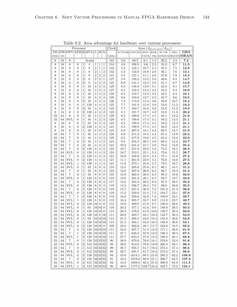
Chapter 8. Soft Vector Processors vs Manual FPGA Hardware Design 134
Table 8.2: Area advantage for hardware over various processorsProcessor Clock Area (Aprocessor/Ahw)
DD DW DPV APB B MVL L M X autcor conven rgb- rgb- ip ch- img- GEO(KB) (B) (MHz) cmyk yiq ecksum blend MEAN
8 16 0 Scalar 143 2.9 69.5 6.1 1.4 20.2 4.3 7.38 16 0 0 1 4 1 1 1 134 4.6 109.5 9.6 2.3 31.9 6.7 11.58 16 0 0 1 8 2 1 1 132 5.2 122.1 10.7 2.5 35.5 7.5 12.98 16 0 0 1 8 2 1 2 132 5.3 124.0 10.8 2.6 36.1 7.6 13.18 16 0 0 1 8 2 2 2 131 5.4 127.1 11.1 2.6 37.0 7.8 13.48 16 0 0 2 8 2 2 1 127 5.9 139.3 12.2 2.9 40.6 8.5 14.78 16 0 0 2 8 2 2 2 125 6.0 141.1 12.3 2.9 41.1 8.7 14.98 16 0 0 1 16 4 2 2 129 6.3 148.9 13.0 3.1 43.3 9.1 15.78 16 0 0 1 16 4 2 4 127 6.5 152.2 13.3 3.2 44.3 9.3 16.08 16 0 0 1 16 4 4 2 128 6.5 152.7 13.3 3.2 44.5 9.4 16.18 16 0 0 1 16 4 4 4 128 6.6 156.8 13.7 3.3 45.7 9.6 16.58 16 0 0 2 16 4 4 2 126 7.4 174.9 15.3 3.6 50.9 10.7 18.48 16 0 0 1 128 4 4 4 125 7.7 181.9 15.9 3.8 53.0 11.2 19.28 16 0 0 2 16 4 4 4 122 7.7 182.7 16.0 3.8 53.2 11.2 19.38 16 0 0 2 128 4 4 2 123 8.1 191.7 16.7 4.0 55.8 11.8 20.232 64 0 0 1 16 4 2 4 129 8.5 199.6 17.4 4.1 58.1 12.2 21.032 64 8VL 0 1 16 4 2 4 129 8.5 199.8 17.4 4.1 58.2 12.3 21.18 16 0 0 1 32 8 4 4 123 8.5 199.8 17.4 4.1 58.2 12.3 21.18 16 0 0 2 128 4 4 4 121 8.5 199.9 17.4 4.1 58.2 12.3 21.18 16 0 0 1 32 8 8 4 124 8.8 207.8 18.1 4.3 60.5 12.7 21.932 64 7 0 1 16 4 4 2 128 8.9 211.0 18.4 4.4 61.4 12.9 22.232 64 7 0 1 16 4 4 4 128 9.2 217.8 19.0 4.5 63.4 13.4 22.932 64 7 0 2 16 4 4 2 124 9.9 234.3 20.5 4.9 68.2 14.4 24.732 64 7 0 2 16 4 4 4 121 10.2 241.3 21.1 5.0 70.2 14.8 25.432 64 7 0 2 128 4 4 2 123 10.7 251.9 22.0 5.2 73.3 15.4 26.532 64 8VL 0 2 128 4 4 2 124 10.7 253.5 22.1 5.3 73.8 15.5 26.732 64 7 0 2 128 4 4 4 121 10.9 258.0 22.5 5.4 75.1 15.8 27.232 64 8VL 0 2 128 4 4 4 121 11.1 261.0 22.8 5.4 76.0 16.0 27.532 64 8VL 1 2 128 4 4 4 121 11.6 273.1 23.8 5.7 79.5 16.7 28.832 64 8VL 0 1 32 8 8 4 123 12.5 295.6 25.8 6.1 86.1 18.1 31.232 64 7 0 1 32 8 8 4 123 12.6 297.8 26.0 6.2 86.7 18.3 31.432 64 7 0 1 32 8 8 8 125 12.9 303.4 26.5 6.3 88.3 18.6 32.032 64 8VL 0 1 128 8 8 8 124 13.6 321.8 28.1 6.7 93.7 19.7 33.932 64 7 0 2 128 8 8 4 117 14.2 334.3 29.2 6.9 97.3 20.5 35.232 64 8VL 0 2 128 8 8 4 119 14.3 336.7 29.4 7.0 98.0 20.6 35.532 64 7 0 2 128 8 8 8 118 14.7 347.5 30.3 7.2 101.2 21.3 36.632 64 8VL 0 2 128 8 8 8 118 15.2 359.6 31.4 7.5 104.7 22.1 37.932 64 7 1 2 128 8 8 8 119 16.0 376.6 32.9 7.8 109.6 23.1 39.732 64 8VL 1 2 128 8 8 8 119 16.4 385.7 33.7 8.0 112.3 23.7 40.732 64 8VL 0 2 128 16 8 8 112 19.9 469.9 41.0 9.7 136.8 28.8 49.532 64 8VL 0 1 64 16 16 8 116 20.2 477.1 41.6 9.9 138.9 29.3 50.332 64 8VL 0 1 128 16 16 8 114 20.3 479.8 41.9 10.0 139.7 29.4 50.632 64 8VL 0 2 128 16 8 16 111 20.9 493.7 43.1 10.2 143.7 30.3 52.032 64 8VL 0 1 64 16 16 16 114 21.2 499.5 43.6 10.4 145.4 30.6 52.632 64 8VL 0 1 128 16 16 16 115 21.4 504.1 44.0 10.5 146.8 30.9 53.132 64 8VL 0 2 128 16 16 8 109 23.8 562.0 49.1 11.7 163.6 34.5 59.232 64 7 0 2 128 16 16 16 111 24.9 587.7 51.3 12.2 171.1 36.0 61.932 64 7 1 2 128 16 16 16 111 27.1 640.3 55.9 13.3 186.4 39.3 67.532 64 8VL 1 2 128 16 16 16 111 27.7 653.2 57.0 13.5 190.2 40.1 68.832 64 7 0 1 128 32 32 32 96 36.9 870.9 76.0 18.1 253.6 53.4 91.832 64 8VL 0 2 512 32 16 32 99 38.8 914.6 79.8 19.0 266.3 56.1 96.432 64 7 0 1 512 32 32 32 99 39.7 935.7 81.7 19.4 272.4 57.4 98.632 64 8VL 0 1 512 32 32 32 99 39.7 935.7 81.7 19.4 272.4 57.4 98.632 64 8VL 0 2 128 32 32 32 94 43.0 1014.1 88.5 21.0 295.2 62.2 106.932 64 7 0 2 128 32 32 32 91 43.2 1019.0 88.9 21.1 296.7 62.5 107.432 64 8VL 0 2 512 32 32 32 92 44.8 1058.0 92.3 21.9 308.0 64.9 111.532 64 8VL 1 2 512 32 32 32 96 49.9 1177.2 102.7 24.4 342.7 72.2 124.1

Chapter 8. Soft Vector Processors vs Manual FPGA Hardware Design 135
Table 8.3: Speed advantage for hardware over various processors.Processor Clock Wall Clock Time (Tprocessor/Thw)
DD DW DPV APB B MVL L M X autcor conven rgb- rgb- ip ch- img- GEO(KB) (B) (MHz) cmyk yiq ecksum blend MEAN
8 16 0 Scalar 143 491.4 2140.3 312.0 621.3 197.6 378.1 497.98 16 0 0 1 4 1 1 1 134 287.0 277.9 233.8 222.4 135.3 259.7 229.48 16 0 0 1 8 2 1 1 132 257.8 204.5 173.1 177.3 95.5 218.9 179.88 16 0 0 1 8 2 1 2 132 220.6 205.3 173.4 144.4 95.3 193.2 166.08 16 0 0 1 8 2 2 2 131 151.6 158.5 141.7 131.6 96.0 159.6 137.88 16 0 0 2 8 2 2 1 127 165.7 161.8 137.4 128.6 89.3 152.9 136.58 16 0 0 2 8 2 2 2 125 149.3 165.3 140.2 111.6 91.1 142.8 130.98 16 0 0 1 16 4 2 2 129 134.4 116.6 115.2 118.0 78.8 129.9 113.98 16 0 0 1 16 4 2 4 127 117.2 118.4 117.0 102.6 80.0 118.8 108.08 16 0 0 1 16 4 4 2 128 102.3 97.5 113.3 107.9 75.1 125.2 102.38 16 0 0 1 16 4 4 4 128 82.7 97.4 113.2 90.6 75.0 111.0 94.08 16 0 0 2 16 4 4 2 126 89.1 98.6 114.9 91.8 72.7 108.0 94.98 16 0 0 1 128 4 4 4 125 81.8 85.5 123.0 93.4 78.5 104.0 93.28 16 0 0 2 16 4 4 4 122 81.8 101.8 118.7 81.6 75.1 103.8 92.58 16 0 0 2 128 4 4 2 123 81.0 74.2 115.9 91.9 73.0 100.2 88.132 64 0 0 1 16 4 2 4 129 115.0 105.2 80.7 74.4 44.9 89.5 81.432 64 8VL 0 1 16 4 2 4 129 115.2 103.2 79.5 69.6 42.9 89.7 79.58 16 0 0 1 32 8 4 4 123 77.0 80.5 114.8 82.2 73.3 100.9 87.08 16 0 0 2 128 4 4 4 121 64.9 75.6 117.9 80.5 74.2 93.8 82.98 16 0 0 1 32 8 8 4 124 58.7 67.8 100.4 74.7 72.3 90.8 76.232 64 7 0 1 16 4 4 2 128 96.7 73.5 51.0 70.2 26.5 68.6 59.932 64 7 0 1 16 4 4 4 128 77.6 73.6 51.1 53.2 26.5 54.9 53.232 64 7 0 2 16 4 4 2 124 85.0 75.4 47.8 54.5 23.6 50.7 52.132 64 7 0 2 16 4 4 4 121 77.1 77.4 49.1 42.7 24.3 44.8 48.932 64 7 0 2 128 4 4 2 123 75.1 50.1 44.8 52.8 22.1 48.1 46.032 64 8VL 0 2 128 4 4 2 124 74.1 48.8 44.2 51.8 20.8 47.0 44.832 64 7 0 2 128 4 4 4 121 60.1 51.1 45.5 40.2 22.4 41.6 41.732 64 8VL 0 2 128 4 4 4 121 60.0 50.3 45.5 39.7 21.4 41.0 41.032 64 8VL 1 2 128 4 4 4 121 60.0 49.8 45.2 38.2 21.4 41.0 40.732 64 8VL 0 1 32 8 8 4 123 53.4 44.4 30.3 37.9 15.1 40.1 34.432 64 7 0 1 32 8 8 4 123 53.4 43.7 29.6 37.9 15.0 36.8 33.632 64 7 0 1 32 8 8 8 125 42.8 42.8 29.1 28.5 14.8 29.1 29.432 64 8VL 0 1 128 8 8 8 124 41.5 35.7 29.5 28.1 15.2 27.9 28.432 64 7 0 2 128 8 8 4 117 43.4 33.1 26.8 29.1 12.8 26.6 26.932 64 8VL 0 2 128 8 8 4 119 42.5 32.0 26.0 27.9 12.0 25.5 25.932 64 7 0 2 128 8 8 8 118 34.3 32.8 26.5 21.8 12.6 22.6 23.932 64 8VL 0 2 128 8 8 8 118 34.3 32.3 26.3 21.3 12.1 22.1 23.432 64 7 1 2 128 8 8 8 119 34.2 32.5 26.4 21.0 12.6 22.6 23.732 64 8VL 1 2 128 8 8 8 119 34.0 31.8 25.8 20.4 12.1 21.9 23.032 64 8VL 0 2 128 16 8 8 112 35.3 32.1 24.8 20.1 11.2 21.1 22.632 64 8VL 0 1 64 16 16 8 116 32.1 29.5 18.7 20.9 10.1 20.7 20.732 64 8VL 0 1 128 16 16 8 114 31.8 26.4 19.5 22.0 9.9 20.5 20.432 64 8VL 0 2 128 16 8 16 111 31.8 32.6 25.0 17.5 11.4 19.8 21.632 64 8VL 0 1 64 16 16 16 114 27.7 30.4 19.2 16.6 10.4 17.4 19.132 64 8VL 0 1 128 16 16 16 115 26.1 26.1 19.3 17.0 9.8 16.5 18.232 64 8VL 0 2 128 16 16 8 109 28.3 26.5 18.2 17.2 8.3 15.8 17.732 64 7 0 2 128 16 16 16 111 23.0 26.6 18.2 13.0 9.4 13.9 16.332 64 7 1 2 128 16 16 16 111 23.0 26.6 18.0 12.6 9.4 14.8 16.432 64 8VL 1 2 128 16 16 16 111 22.9 25.9 17.5 12.9 8.1 13.5 15.732 64 7 0 1 128 32 32 32 96 22.0 25.3 15.7 11.9 9.5 12.7 15.232 64 8VL 0 2 512 32 16 32 99 23.7 24.2 18.3 11.5 10.6 12.0 15.832 64 7 0 1 512 32 32 32 99 21.9 21.2 16.3 12.3 11.4 11.7 15.232 64 8VL 0 1 512 32 32 32 99 21.9 21.0 15.6 12.0 10.3 10.6 14.532 64 8VL 0 2 128 32 32 32 94 21.9 25.7 18.3 12.5 7.7 10.4 14.732 64 7 0 2 128 32 32 32 91 22.6 26.7 16.1 10.4 9.0 11.1 14.732 64 8VL 0 2 512 32 32 32 92 20.4 21.6 15.2 10.1 10.0 9.1 13.532 64 8VL 1 2 512 32 32 32 96 19.7 21.0 14.5 9.5 9.5 8.8 13.0

Chapter 8. Soft Vector Processors vs Manual FPGA Hardware Design 136
the top row of the table which divides the processor area by the hardware area. The
configurations are sorted by their areas with the smallest area designs at the top of the
table and the largest at the bottom. Since no instruction set subsetting or width reduction
is performed in this section (these customizations will be evaluated in Section 8.5), the
area of the processors are the same for each benchmark, however the area of the hardware
circuit that implements each benchmark varies significantly. The first row shows the
hardware area advantage over the scalar processor varies between 1.4x for the rgbyiq
benchmark and 69.5x for conven which is extremely small in hardware due to its 1-bit
datapath.
The geometrically averaged mean across the benchmark indicates a scalar soft proces-
sor is 7.3x bigger than a hardware circuit on average. The second row shows that adding
minimum support for vector extensions creates a VESPA processor which is 11.5x larger
than hardware. Thus, both processors require significantly more area than a custom-
built hardware circuit. This is partly due to the simplifying assumptions made resulting
in incomplete hardware circuits, but is also due to the general purpose processing capa-
bilities of the processors. Both processors can perform any 32-bit computation on data
organized in any pattern in memory (without requiring alignment). The hardware how-
ever performs only a very specific task, and due to the simplicity in these benchmarks,
this is often a very small task which leads to circuits with small areas. We would expect
more complicated benchmarks to require significantly more area than these six, however
certain overheads are specific to the processors and can be avoided in hardware: the
caches for hiding memory latency, the register file shared by all functional units, and
the instruction fetch and decode logic contribute to additional area not required in the
hardware circuits. These area overheads can be amortized over the many vector lanes as
is the case for the largest VESPA configuration which has 32 lanes and is 124.1x larger
than the hardware circuits. However the lanes themselves contain significant overheads
in supporting a variety of operations and fixed 32-bit precision. Both of these are elimi-
nated in Section 8.5 using the instruction set subsetting and width reduction techniques
Chapter 8. Soft Vector Processors vs Manual FPGA Hardware Design 137
from the previous chapter.
8.4.2 Software vs Hardware: Wall Clock Speed
Table 8.3 shows the wall clock speed advantage of the hardware over the processors.
The slowest processors are at the top of the table and fastest at the bottom. Focusing
on the first row of the table, we observe that the scalar processor executing out-of-the-
box C code performs approximately 500x slower than hardware. The primary cause of
the under-performance is failing to exploit the available data parallelism, except for the
conven benchmark which performs extraordinarily worse in software. This benchmark
performs different array operations depending on the values in a small matrix. Each array
operation requires load and store operations to fetch each array element and write it back
to memory. In hardware the elements are only fetched once and stored internally in flip
flops removing this memory access overhead as well as loop overheads resulting in a 2140x
hardware speedup. The scalar processor is relatively more competitive with the very
simple ip checksum benchmark performing 197.6x slower than hardware. Nonetheless
the speed gap is shown to be very large between the hardware and scalar soft processor.
It is hence not surprising that current commercial soft processors are used predominantly
for system control tasks, while hardware design is necessary for most computational tasks
on an FPGA.
The slowest VESPA configuration is on average 229.4x slower than hardware, while
the fastest configuration can dramatically reduce this performance gap to just 13x as seen
in the last row of Table 8.3. Though this is still a significant performance gap, it makes
a soft vector processor far more likely to be used for implementing a non-critical data
parallel compute task than a scalar soft processor. The performance certainly does not
match that of hardware design, and the area cost is significant as seen in the previous
section, but the ease of programming a soft vector processor versus designing custom
hardware can make a soft vector processor an effective implementation vehicle for data
parallel workloads. Thus, the addition of vector processor extensions to commercial soft
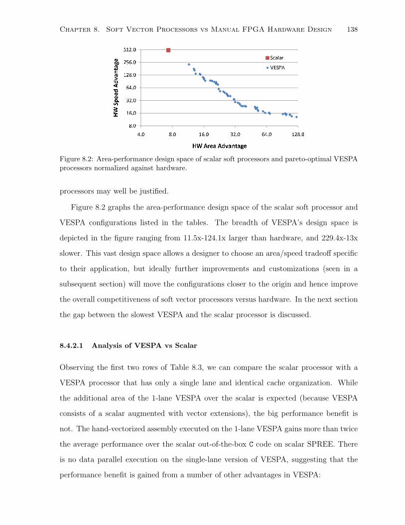
Chapter 8. Soft Vector Processors vs Manual FPGA Hardware Design 138
8.0
16.0
32.0
64.0
128.0
256.0
512.0
4.0 8.0 16.0 32.0 64.0 128.0
HW Speed Advantage
HW Area Advantage
Scalar
VESPA
Figure 8.2: Area-performance design space of scalar soft processors and pareto-optimal VESPAprocessors normalized against hardware.
processors may well be justified.
Figure 8.2 graphs the area-performance design space of the scalar soft processor and
VESPA configurations listed in the tables. The breadth of VESPA’s design space is
depicted in the figure ranging from 11.5x-124.1x larger than hardware, and 229.4x-13x
slower. This vast design space allows a designer to choose an area/speed tradeoff specific
to their application, but ideally further improvements and customizations (seen in a
subsequent section) will move the configurations closer to the origin and hence improve
the overall competitiveness of soft vector processors versus hardware. In the next section
the gap between the slowest VESPA and the scalar processor is discussed.
8.4.2.1 Analysis of VESPA vs Scalar
Observing the first two rows of Table 8.3, we can compare the scalar processor with a
VESPA processor that has only a single lane and identical cache organization. While
the additional area of the 1-lane VESPA over the scalar is expected (because VESPA
consists of a scalar augmented with vector extensions), the big performance benefit is
not. The hand-vectorized assembly executed on the 1-lane VESPA gains more than twice
the average performance over the scalar out-of-the-box C code on scalar SPREE. There
is no data parallel execution on the single-lane version of VESPA, suggesting that the
performance benefit is gained from a number of other advantages in VESPA:
Chapter 8. Soft Vector Processors vs Manual FPGA Hardware Design 139
1. Amortization of loop control instructions. The loop control instructions are
executed far less often in VESPA than in the scalar.
2. More register storage. The large vector register file can store and manipulate
arrays without having to access the cache or memory.
3. More efficient pipelining. VESPA executes batches of operations with no de-
pendencies, meaning the pipeline can process these without stalling due to hazards.
4. Instruction support. VESPA has direct support for fixed-point operations, pred-
ication, and built-in min/max/absolute instructions from the VIRAM instruction
set.
5. Simultaneous execution across multiple pipelines. In VESPA scalar opera-
tions are executed in the scalar pipeline, vector control operations are executed in
the vector control pipeline, and vector operations in the vector pipeline. All three
of these execute out-of-order with respect to each other.
6. Assembly-level optimization. Manual vectorization in assembly may have lead
to optimizations beyond the C-compiled scalar output from GCC.
Determining the exact contribution of each advantage is beyond the scope of this work.
We instead perform some qualitative analysis: Closer inspection of conven revealed the
cause of the 9x performance boost seen on the single lane VESPA to be the repeated
operations performed on a single array. In VESPA the large vector register file can store
large array chunks and manipulate them without storing and re-reading them from cache
as the scalar processor must. The other benchmarks are less impacted because of their
streaming and low-reuse nature. The loop overhead amortization gained by performing
64 loop iterations (MVL=64) at once significantly impacts benchmarks with small loop
bodies such as autcor, conven, ip checksum, and imgblend. The more powerful
VIRAM instruction set with fixed-point support further reduced the loop bodies of aut-
cor and rgbcmyk. Finally, the disassembled GCC output did not appear significantly
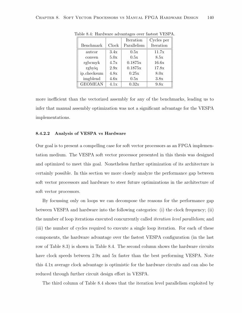
Chapter 8. Soft Vector Processors vs Manual FPGA Hardware Design 140
Table 8.4: Hardware advantages over fastest VESPA.Iteration Cycles per
Benchmark Clock Parallelism Iterationautcor 3.4x 0.5x 11.7xconven 5.0x 0.5x 8.5x
rgbcmyk 4.7x 0.1875x 16.6xrgbyiq 2.9x 0.1875x 17.8x
ip checksum 4.8x 0.25x 8.0ximgblend 4.6x 0.5x 3.8x
GEOMEAN 4.1x 0.32x 9.8x
more inefficient than the vectorized assembly for any of the benchmarks, leading us to
infer that manual assembly optimization was not a significant advantage for the VESPA
implementations.
8.4.2.2 Analysis of VESPA vs Hardware
Our goal is to present a compelling case for soft vector processors as an FPGA implemen-
tation medium. The VESPA soft vector processor presented in this thesis was designed
and optimized to meet this goal. Nonetheless further optimization of its architecture is
certainly possible. In this section we more closely analyze the performance gap between
soft vector processors and hardware to steer future optimizations in the architecture of
soft vector processors.
By focussing only on loops we can decompose the reasons for the performance gap
between VESPA and hardware into the following categories: (i) the clock frequency; (ii)
the number of loop iterations executed concurrently called iteration level parallelism; and
(iii) the number of cycles required to execute a single loop iteration. For each of these
components, the hardware advantage over the fastest VESPA configuration (in the last
row of Table 8.3) is shown in Table 8.4. The second column shows the hardware circuits
have clock speeds between 2.9x and 5x faster than the best performing VESPA. Note
this 4.1x average clock advantage is optimistic for the hardware circuits and can also be
reduced through further circuit design effort in VESPA.
The third column of Table 8.4 shows that the iteration level parallelism exploited by

Chapter 8. Soft Vector Processors vs Manual FPGA Hardware Design 141
the hardware is less than or equal to that exploited by VESPA which is 32 for all bench-
marks since there are 32 lanes in the chosen configuration. But in the hardware circuits
we matched the parallelism to the memory bandwidth. For example, the ip checksum
benchmark operates on a stream of 16-bit elements meaning in a given DRAM access
only 8 elements can be retrieved from memory. The circuit is hence designed to have
only 8-way parallelism. If the memory was widened further the hardware circuit would
more effectively utilize the additional bandwidth than VESPA.
The last column gives the speedup of executing a single loop iteration in hardware
over VESPA and is calculated from the measured overall speedups in the last row of
Table 8.3 divided by the clock and iteration parallelism advantages. This component
represents the cycle inefficiencies in the VESPA architecture much of which is inherent
in any processor-style architecture. We list these inefficiencies below:
1. Limited register ports – Only a few data operands can be retrieved in a given
clock cycle. This limits the number of instructions that can be ready for execution.
Hardware design does not require a centralized register file and hence avoids this
limitation.
2. Limited functional units – Only a few operations can be performed in a given
clock cycle. In hardware a designer can instantiate as many dedicated processing
elements as necessary.
3. Limited cache access ports – Only one cache line can be retrieved in a given
clock cycle. In hardware a designer can distribute data into any organization that
meets the needs of an application.
4. Imperfect prefetching – Ideally all memory latency can be hidden.
Overcoming the first two inefficiencies would allow many instruction to be simulta-
neously executed which more closely resembles the spatial computation performed by
the hardware circuit. In addition, perfect prefetching and multiple cache ports would
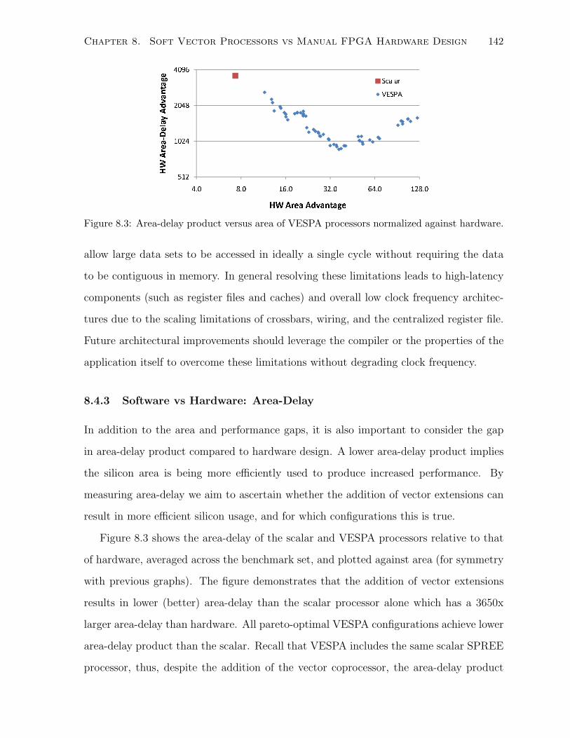
Chapter 8. Soft Vector Processors vs Manual FPGA Hardware Design 142
512
1024
2048
4096
4.0 8.0 16.0 32.0 64.0 128.0
HW Area-Delay Advantage
HW Area Advantage
Scalar
VESPA
Figure 8.3: Area-delay product versus area of VESPA processors normalized against hardware.
allow large data sets to be accessed in ideally a single cycle without requiring the data
to be contiguous in memory. In general resolving these limitations leads to high-latency
components (such as register files and caches) and overall low clock frequency architec-
tures due to the scaling limitations of crossbars, wiring, and the centralized register file.
Future architectural improvements should leverage the compiler or the properties of the
application itself to overcome these limitations without degrading clock frequency.
8.4.3 Software vs Hardware: Area-Delay
In addition to the area and performance gaps, it is also important to consider the gap
in area-delay product compared to hardware design. A lower area-delay product implies
the silicon area is being more efficiently used to produce increased performance. By
measuring area-delay we aim to ascertain whether the addition of vector extensions can
result in more efficient silicon usage, and for which configurations this is true.
Figure 8.3 shows the area-delay of the scalar and VESPA processors relative to that
of hardware, averaged across the benchmark set, and plotted against area (for symmetry
with previous graphs). The figure demonstrates that the addition of vector extensions
results in lower (better) area-delay than the scalar processor alone which has a 3650x
larger area-delay than hardware. All pareto-optimal VESPA configurations achieve lower
area-delay product than the scalar. Recall that VESPA includes the same scalar SPREE
processor, thus, despite the addition of the vector coprocessor, the area-delay product
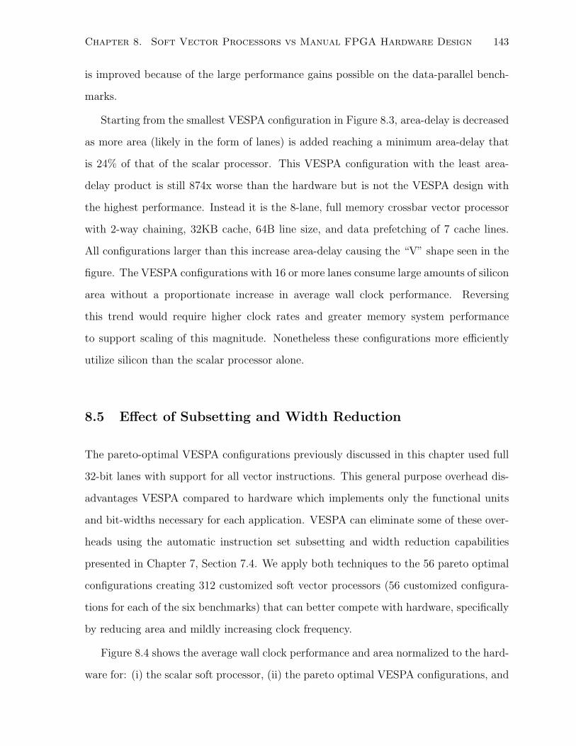
Chapter 8. Soft Vector Processors vs Manual FPGA Hardware Design 143
is improved because of the large performance gains possible on the data-parallel bench-
marks.
Starting from the smallest VESPA configuration in Figure 8.3, area-delay is decreased
as more area (likely in the form of lanes) is added reaching a minimum area-delay that
is 24% of that of the scalar processor. This VESPA configuration with the least area-
delay product is still 874x worse than the hardware but is not the VESPA design with
the highest performance. Instead it is the 8-lane, full memory crossbar vector processor
with 2-way chaining, 32KB cache, 64B line size, and data prefetching of 7 cache lines.
All configurations larger than this increase area-delay causing the “V” shape seen in the
figure. The VESPA configurations with 16 or more lanes consume large amounts of silicon
area without a proportionate increase in average wall clock performance. Reversing
this trend would require higher clock rates and greater memory system performance
to support scaling of this magnitude. Nonetheless these configurations more efficiently
utilize silicon than the scalar processor alone.
8.5 Effect of Subsetting and Width Reduction
The pareto-optimal VESPA configurations previously discussed in this chapter used full
32-bit lanes with support for all vector instructions. This general purpose overhead dis-
advantages VESPA compared to hardware which implements only the functional units
and bit-widths necessary for each application. VESPA can eliminate some of these over-
heads using the automatic instruction set subsetting and width reduction capabilities
presented in Chapter 7, Section 7.4. We apply both techniques to the 56 pareto optimal
configurations creating 312 customized soft vector processors (56 customized configura-
tions for each of the six benchmarks) that can better compete with hardware, specifically
by reducing area and mildly increasing clock frequency.
Figure 8.4 shows the average wall clock performance and area normalized to the hard-
ware for: (i) the scalar soft processor, (ii) the pareto optimal VESPA configurations, and
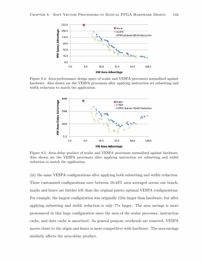
Chapter 8. Soft Vector Processors vs Manual FPGA Hardware Design 144
8.0
16.0
32.0
64.0
128.0
256.0
512.0
4.0 8.0 16.0 32.0 64.0 128.0
HW Speed Advantage
HW Area Advantage
Scalar
VESPA
VESPA+Subset+Width Reduction
Figure 8.4: Area-performance design space of scalar and VESPA processors normalized againsthardware. Also shown are the VESPA processors after applying instruction set subsetting andwidth reduction to match the application.
512
1024
2048
4096
4.0 8.0 16.0 32.0 64.0 128.0
HW Area-Delay Advantage
HW Area Advantage
Scalar
VESPA
VESPA+Subset+Width Reduction
Figure 8.5: Area-delay product of scalar and VESPA processors normalized against hardware.Also shown are the VESPA processors after applying instruction set subsetting and widthreduction to match the application.
(iii) the same VESPA configurations after applying both subsetting and width reduction.
These customized configurations save between 10-43% area averaged across our bench-
marks and hence are further left than the original pareto optimal VESPA configurations.
For example, the largest configuration was originally 124x larger than hardware, but after
applying subsetting and width reduction is only 77x larger. The area savings is more
pronounced in this large configuration since the area of the scalar processor, instruction
cache, and data cache is amortized. As general purpose overheads are removed, VESPA
moves closer to the origin and hence is more competitive with hardware. The area savings
similarly affects the area-delay product.
Chapter 8. Soft Vector Processors vs Manual FPGA Hardware Design 145
Figure 8.5 shows the area-delay versus area plot of the same three data series. The
subsetting and width reduction customizations reduce area and hence area-delay result-
ing in VESPA configurations which are both further left and down than the original
corresponding pareto optimal configurations. The lowest achievable area-delay is still
620x larger than hardware but is significantly smaller than the 874x area-delay without
subsetting and width reduction. Interestingly, the configuration that achieves the 620x
area-delay is not the same 8-lane VESPA discussed in the last section. Instead it is a
16-lane VESPA with no chaining, full memory crossbar, 32KB data cache, 64B line size,
and prefetching of 8V L cache lines. Thus, by reducing the area cost of adding more lanes
we further enable many-lane configurations to efficiently trade area for performance.
8.6 Summary
This chapter described the manual hardware implementations of our benchmarks which
we used to compare against VESPA and a scalar soft processor without vector extensions.
The scalar was shown to be 500x slower than the hardware while VESPA can reduce this
performance gap to 13x, although the area is increased from 7.3x to 124x. Nonetheless
this area growth results in improved area-delay over the scalar soft processor. In the
best case area-delay is reduced from 3650x to 874x larger than hardware. Furthermore
subsetting and width reduction can be applied to save up to 43% area and reduce area-
delay to 620x compared to hardware. While the gaps between VESPA and hardware
remain large, they have been reduced considerably compared to the scalar soft processor.
Further optimization of the VESPA architecture can continue to close the gap, however
our idealized simplifications for the hardware circuits suggest these measurements likely
upper bounds on the advantages of hardware design. As a result, soft vector processors
are adequately motivated since an FPGA designer is more likely to implement a data
parallel computation in software if hardware can at best outperform the soft processor
by only 13x.
Chapter 9
Conclusions
FPGAs are increasingly used to implement complex digital systems, but the design of
such systems is difficult due to the laborious hardware descriptions necessary for efficient
FPGA implementation. A microprocessor can be used to more easily implement compu-
tation in a high-level programming language. Because of the performance overheads asso-
ciated with a microprocessor it is limited to implementing system control and non-critical
computation tasks. In fact, this microprocessor is often a soft processor implemented in
the reprogrammable fabric hence inheriting both FPGA and processor overheads. The
added overhead results in further inefficiencies in area/performance/power making soft
processors useful for only the least critical computation tasks. Nonetheless, a soft proces-
sor is useful because it preserves the benefits of a single-chip solution without specializing
the FPGA device and increasing its cost. By improving soft processors and offseting these
overheads, more computation can be designed in software and executed on a soft proces-
sor without the long hardware design times and without heavy area/performance/power
penalties.
In this thesis, we improve soft processors by allowing their architecture to respond
to characteristics in the application. Specifically, we focus on the amount of data level
parallelism in an application, which is a property found in many embedded and mul-
timedia applications. We propose that soft vector processors can be used to efficiently
146
Chapter 9. Conclusions 147
scale performance for such applications, hence suggesting that current soft processors be
augmented with vector extensions. This increased performance can be used to justify
the implementation of more critical computation in a soft vector processor rather than
using manual hardware design. As more computation is implemented with relative ease
using sequential programming, we achieve our goal of simplifying FPGA design.
Through experimentation with real benchmarks and real hardware implementations,
we validate the feasibility of soft vector processors hence making a compelling case for
the inclusion of vector extensions in current soft processors. We consider the soft vector
processor successful if it can take advantage of the FPGA reprogrammable fabric to:
(i) scale performance when executing data parallel workloads; (ii) precisely control the
area/performance tradeoff; and (iii) customize the functionality and area overheads to a
given application. To this end we make the following contributions.
9.1 Contributions
1. VESPA Infrastructure – A proof-of-concept soft vector processor called VESPA
was designed and implemented on real FPGA hardware, executing industry-standard
embedded benchmarks from off-chip commodity DRAM. The VESPA processor, its
ported GNU assembler, and instruction set simulator are valuable infrastructure
components for enabling future research into soft vector processors.
2. Performance Scalability – VESPA was shown to scale up to 32 vector lanes
on real FPGA hardware achieving up to 26.5x speedup over 1 lane using data
parallel benchmarks from the industry-standard EEMBC suite. Much of this scaling
was enabled through improvements to the memory system which were necessary to
sustain performance scaling for many vector lanes.
3. Architectural Parameters – To precisely control the area and performance trade-
off, many architectural parameters were implemented for modifying the compute
architecture, interface, and memory system of the soft vector processor. In addition

Chapter 9. Conclusions 148
to the cache configuration and prefetching strategy, VESPA also has a parameter-
ized maximum vector length and number of lanes in the architecture. Beyond these,
VESPA can be customized to the instruction mix allowing the designer to reduce the
number of lanes with multiply functional units and access to the memory crossbar.
Applications with low demand of the multiplier or memory can have area saved
with minimal performance loss. Performance within each lane can be increased
using the parameterized support for vector chaining. VESPA can simultaneously
execute multiple chained vector instructions using a banked register file. All three
VESPA functional units can potentially be active, and the number of ALUs can
also be replicated to enable further scaling.
4. Design Space Exploration – To demonstrate that the architectural variations in a
soft vector processor can be used to gain fine-grain control of area and performance,
we explore the VESPA design space through 768 configurations. VESPA was shown
to finely span a broad 28x range in area, 24x in cycle performance, and 18x in wall
clock time due to the clock frequency degradation caused by instantiating many
lanes. Of these 768 configurations, the 56 configurations found to be pareto optimal
employed different combinations of all VESPA parameters, showing that each of
these architectural variations can be useful to an FPGA designer. Moreover it was
shown that performance-per-area gains can be achieved by choosing a configuration
on a per-application basis.
5. Customizing Functionality – An important feature of soft processors is their
ability to deliver exactly the functionality required by the application without added
overheads. VESPA supports this through automatic subsetting of the instruction
set by parsing the application binary and removing hardware support for unused
instructions. Also, the width of the lanes can be reduced from the 32-bit default
to match the precision required by an application down to 1-bit. The combination
of these two customizations can dramatically reduce the area of the VESPA vector
Chapter 9. Conclusions 149
coprocessor by up to 78%, on average 47%.
6. VESPA Versus Hardware Comparison – Although soft vector processors were
shown to scale performance, span a broad design space, and customize their func-
tionality, an FPGA designer must still consider that better area and performance
can be achieved with manual hardware design. By quantifying the area and per-
formance gaps between soft vector processors and hardware design we can better
inform FPGA designers as well as benchmark the progress made with VESPA. A
scalar soft processor was shown to perform 500x slower than hardware while the
VESPA soft vector processor can reduce this performance gap to 13x. These mea-
surements were made with idealized hardware implementations of our benchmarks
and are hence upper bounds on the advantages of hardware design. In terms of
area-delay product, scalar soft processors are 3650x worse than custom hardware
design, while all pareto-optimal VESPA configurations improve on this. This sug-
gests that the addition of vector extensions to a scalar soft processor makes it more
efficient for data parallel workloads. The most efficient configuration reduces the
3650x area-delay gap to 874x without customization, and to 620x after unneeded
instruction support and datapath width are removed.
In conclusion, the scalable performance provided by soft vector processors allows
FPGA designers to meet their performance constraints without resorting to more difficult
hardware design. This simplifies FPGA design since for a given digital system, the
overal design time is reduced by leveraging the high-level programming languages and
single-step debug infrastructure in software. Efficiency can be gained by performing
fine-grain matching of the architecture of the soft vector processor to the needs of the
application. Additionally, the soft vector processor can also be customized to support
only the functionality required by the application to save area.
Chapter 9. Conclusions 150
9.2 Future Work
Although VESPA was already used to thoroughly investigate the feasibility of soft vector
processors, there are several new avenues of research enabled by this thesis.
Improving the VESPA Architecture – In terms of improving VESPA, the clock
frequency and memory unit can be improved to make it significantly more powerful. The
VESPA clock frequency is in the same range as the scalar SPREE processor it is based
off of, which runs at 143 MHz, while the Altera Nios II can be clocked at 250 MHz on the
same device. A faster clock rate may not translate to proportionally higher performance,
but is necessary for designs with higher system clocks to avoid clock crossing delays.
The memory system is pipelined but currently has one cycle start latency and one cycle
end latency. These delays can be removed by better integrating the memory system
into the VESPA pipeline or implementing a non-blocking cache. Either of these options
would improve the impact of scaling across lanes and vector chaining. Alternatively,
radically different vector architectures such as the CODE [34] vector processor could be
implemented. Simultaneous with high-level architectural modifications, a generator tool
could also consider low-level circuit optimizations which are imperative for supporting
certain configurations. For example, much of the clock frequency degradation in the
32-lane VESPA could be eliminated with more careful re-engineering within the pipeline.
Auto-Vectorizing Compiler Support – The key attribute of VESPA over hard-
ware design is its software interface making it easier to program and debug. In this
thesis manual programming at the assembly-level was necessary to program VESPA. Al-
though this is still very much easier than hardware design, ideally vectorization should be
performed in the compiler from a high-level programming language. Successfully imple-
menting this software toolchain would further promote the adoption of vector processing
extensions in soft processors.
Custom Instructions – VESPA provides several methods of customizing the soft
vector processor by removing hardware, but additional interesting research may be per-
formed by adding new hardware to VESPA. An example of this is the option of adding a
Chapter 9. Conclusions 151
custom functional unit to each lane which simultaneously exploits custom computation
and data parallelism. Another example similar to Yu et. al. [75] is to include lane-local
scratchpad memories, or dedicated instructions for reduction operations. Other more
generically useful operations can be explored and included in VESPA.
Architecture Selection Heuristics – The expansive VESPA design space moti-
vates exciting research into the automatic configuration of a soft vector processor. This
thesis showed that choosing a per-application configuration can result in significantly
more efficient soft vector processors, but searching this configuration space with tens of
thousands of possible configurations is infeasible for FPGA designers under tight time-to-
market constraints. Tools for automatically selecting a configuration given an application
would enable designers to take advantage of the many architectural parameters without
evaluating each configuration. One possible such method is to include in-hardware pro-
filing to extract characteristics of the program behaviour and use heuristics for mapping
these to a vector architecture configuration.
System-Level Tradeoffs – Soft vector processors are effective for data parallel code,
but other processor architectures may be required for better exploiting other code char-
acteristics. The integration of VESPA with a SPREE processor allows it to be included
in the SPREE framework enabling simultaneous exploration of vector and scalar soft pro-
cessor architectures. Such a framework allows system-level optimizations to be performed
to best match the needs of the overall FPGA system.
High Performance Computing – VESPA makes a significant impact for current
embedded FPGA system designers, but FPGAs are also useful in other computing do-
mains such as in high-performance computing (HPC). VESPA can be used in this domain
to provide scientists with a familiar vector processor interface reminiscent of previous vec-
tor supercomputers. The addition of floating point instructions is necessary for many
HPC applications, but most importantly, these systems would need to provide scaling
far beyond 32 lanes. Research in such an architecture and its memory system provides
opportunity for interesting innovations as it likely spans multiple FPGA devices.
Appendix A
Measured Model Parameters
In chapter 4 we modelled a perfect memory system by extrapolating a model based
on a few input parameters measured from the program behaviour. Specifically, the
input parameters were: (i) the frequency of load instruction; (ii) the load miss rates
on various sized direct-mapped data caches with 16B line size; (iii) the frequency of store
instructions; and (iv) the store miss rates on various sized direct-mapped data caches
with 16B line size.
These input parameters were measured across 46 EEMBC benchmarks using the
MINT simulator. MINT was augmented with counters for tracking the number of total
instructions, load instructions, and store instructions. These measurements were used
to calculate the frequency of loads and stores in the instruction stream. MINT was also
augmented with a model of a direct-mapped cache with 16B line size and parameterized
depth. This model was used to count hits and misses in the data cache and derive the
load and store miss rates for caches ranging from 256B to 1MB. The tables below list
the values collected for loads and stores respectively.
152

Appendix A. Measured Model Parameters 153
Table A.1: Load frequency and miss rates across cache size for EEMBC benchmarks.Load Load Miss Rate for Given Cache Size
Frequency 256B 1KB 4KB 16KB 64KB 256KB 1MB
a2time01 0.036 0.140 0.022 0.003 0.000 0.000 0.000 0.000aifftr01 0.186 0.867 0.857 0.561 0.029 0.002 0.000 0.000aifirf01 0.201 0.266 0.158 0.137 0.000 0.000 0.000 0.000aiifft01 0.189 0.893 0.883 0.578 0.028 0.002 0.000 0.000basefp01 0.061 0.029 0.010 0.001 0.000 0.000 0.000 0.000bitmnp01 0.051 0.109 0.052 0.008 0.000 0.000 0.000 0.000cacheb01 0.206 0.269 0.107 0.053 0.027 0.000 0.000 0.000canrdr01 0.124 0.430 0.103 0.031 0.001 0.000 0.000 0.000idctrn01 0.171 0.258 0.075 0.030 0.000 0.000 0.000 0.000iirflt01 0.040 0.213 0.108 0.071 0.000 0.000 0.000 0.000matrix01 0.090 0.055 0.034 0.023 0.003 0.000 0.000 0.000puwmod01 0.151 0.170 0.032 0.002 0.000 0.000 0.000 0.000rspeed01 0.171 0.106 0.041 0.008 0.000 0.000 0.000 0.000tblook01 0.099 0.076 0.034 0.003 0.001 0.000 0.000 0.000bezier01fixed 0.046 0.044 0.036 0.034 0.010 0.000 0.000 0.000dither01 0.130 0.282 0.200 0.021 0.014 0.002 0.000 0.000rotate01 0.058 0.513 0.308 0.161 0.030 0.000 0.000 0.000text01 0.157 0.379 0.156 0.099 0.041 0.000 0.000 0.000autcor00data 2 0.200 0.063 0.063 0.000 0.000 0.000 0.000 0.000conven00data 1 0.158 0.067 0.021 0.000 0.000 0.000 0.000 0.000fbital00data 2 0.061 0.238 0.164 0.031 0.031 0.000 0.000 0.000fft00data 3 0.130 0.780 0.076 0.002 0.000 0.000 0.000 0.000viterb00data 2 0.162 0.075 0.018 0.016 0.000 0.000 0.000 0.000ip pktcheckb4m 0.191 0.146 0.117 0.109 0.107 0.093 0.040 0.012ip reassembly 0.264 0.383 0.265 0.190 0.156 0.143 0.127 0.074nat 0.160 0.356 0.256 0.225 0.179 0.177 0.158 0.000ospfv2 0.187 0.728 0.508 0.063 0.020 0.000 0.000 0.000qos 0.233 0.240 0.002 0.001 0.000 0.000 0.000 0.000routelookup 0.244 0.377 0.219 0.044 0.008 0.000 0.000 0.000tcpbulk 0.133 0.201 0.181 0.120 0.075 0.013 0.000 0.000tcpjumbo 0.180 0.172 0.169 0.168 0.103 0.022 0.000 0.000tcpmixed 0.089 0.253 0.178 0.132 0.081 0.022 0.000 0.000aes 0.143 0.274 0.121 0.000 0.000 0.000 0.000 0.000cjpegv2data5 0.182 0.362 0.284 0.095 0.030 0.017 0.011 0.008des 0.204 0.776 0.463 0.004 0.003 0.000 0.000 0.000djpegv2data6 0.178 0.420 0.259 0.104 0.034 0.015 0.008 0.003huffde 0.078 0.681 0.521 0.215 0.042 0.014 0.000 0.000mp2decoddata1 0.169 0.157 0.073 0.033 0.014 0.010 0.009 0.005mp2enfixdata1 0.222 0.174 0.084 0.010 0.004 0.003 0.003 0.002mp3playerfixeddata2 0.221 0.373 0.174 0.086 0.023 0.009 0.006 0.006mp4decodedata4 0.144 0.211 0.096 0.060 0.032 0.026 0.015 0.004mp4encodedata3 0.217 0.260 0.113 0.037 0.013 0.009 0.006 0.002rgbcmykv2data5 0.103 0.082 0.067 0.064 0.063 0.063 0.063 0.063rgbhpgv2data5 0.232 0.115 0.031 0.009 0.007 0.006 0.006 0.001rgbyiqv2data5 0.038 0.271 0.063 0.063 0.063 0.063 0.063 0.063rsa 0.115 0.231 0.070 0.013 0.005 0.005 0.000 0.000
AVERAGE 0.148 0.295 0.171 0.081 0.028 0.016 0.011 0.005
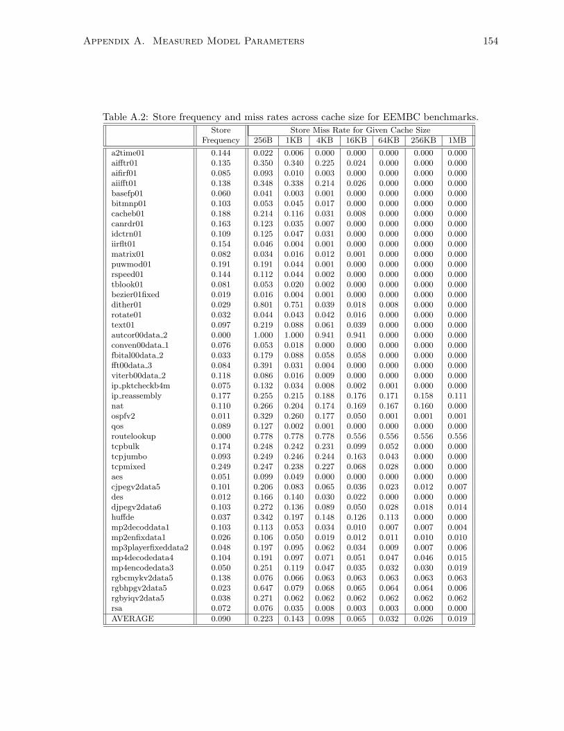
Appendix A. Measured Model Parameters 154
Table A.2: Store frequency and miss rates across cache size for EEMBC benchmarks.Store Store Miss Rate for Given Cache Size
Frequency 256B 1KB 4KB 16KB 64KB 256KB 1MB
a2time01 0.144 0.022 0.006 0.000 0.000 0.000 0.000 0.000aifftr01 0.135 0.350 0.340 0.225 0.024 0.000 0.000 0.000aifirf01 0.085 0.093 0.010 0.003 0.000 0.000 0.000 0.000aiifft01 0.138 0.348 0.338 0.214 0.026 0.000 0.000 0.000basefp01 0.060 0.041 0.003 0.001 0.000 0.000 0.000 0.000bitmnp01 0.103 0.053 0.045 0.017 0.000 0.000 0.000 0.000cacheb01 0.188 0.214 0.116 0.031 0.008 0.000 0.000 0.000canrdr01 0.163 0.123 0.035 0.007 0.000 0.000 0.000 0.000idctrn01 0.109 0.125 0.047 0.031 0.000 0.000 0.000 0.000iirflt01 0.154 0.046 0.004 0.001 0.000 0.000 0.000 0.000matrix01 0.082 0.034 0.016 0.012 0.001 0.000 0.000 0.000puwmod01 0.191 0.191 0.044 0.001 0.000 0.000 0.000 0.000rspeed01 0.144 0.112 0.044 0.002 0.000 0.000 0.000 0.000tblook01 0.081 0.053 0.020 0.002 0.000 0.000 0.000 0.000bezier01fixed 0.019 0.016 0.004 0.001 0.000 0.000 0.000 0.000dither01 0.029 0.801 0.751 0.039 0.018 0.008 0.000 0.000rotate01 0.032 0.044 0.043 0.042 0.016 0.000 0.000 0.000text01 0.097 0.219 0.088 0.061 0.039 0.000 0.000 0.000autcor00data 2 0.000 1.000 1.000 0.941 0.941 0.000 0.000 0.000conven00data 1 0.076 0.053 0.018 0.000 0.000 0.000 0.000 0.000fbital00data 2 0.033 0.179 0.088 0.058 0.058 0.000 0.000 0.000fft00data 3 0.084 0.391 0.031 0.004 0.000 0.000 0.000 0.000viterb00data 2 0.118 0.086 0.016 0.009 0.000 0.000 0.000 0.000ip pktcheckb4m 0.075 0.132 0.034 0.008 0.002 0.001 0.000 0.000ip reassembly 0.177 0.255 0.215 0.188 0.176 0.171 0.158 0.111nat 0.110 0.266 0.204 0.174 0.169 0.167 0.160 0.000ospfv2 0.011 0.329 0.260 0.177 0.050 0.001 0.001 0.001qos 0.089 0.127 0.002 0.001 0.000 0.000 0.000 0.000routelookup 0.000 0.778 0.778 0.778 0.556 0.556 0.556 0.556tcpbulk 0.174 0.248 0.242 0.231 0.099 0.052 0.000 0.000tcpjumbo 0.093 0.249 0.246 0.244 0.163 0.043 0.000 0.000tcpmixed 0.249 0.247 0.238 0.227 0.068 0.028 0.000 0.000aes 0.051 0.099 0.049 0.000 0.000 0.000 0.000 0.000cjpegv2data5 0.101 0.206 0.083 0.065 0.036 0.023 0.012 0.007des 0.012 0.166 0.140 0.030 0.022 0.000 0.000 0.000djpegv2data6 0.103 0.272 0.136 0.089 0.050 0.028 0.018 0.014huffde 0.037 0.342 0.197 0.148 0.126 0.113 0.000 0.000mp2decoddata1 0.103 0.113 0.053 0.034 0.010 0.007 0.007 0.004mp2enfixdata1 0.026 0.106 0.050 0.019 0.012 0.011 0.010 0.010mp3playerfixeddata2 0.048 0.197 0.095 0.062 0.034 0.009 0.007 0.006mp4decodedata4 0.104 0.191 0.097 0.071 0.051 0.047 0.046 0.015mp4encodedata3 0.050 0.251 0.119 0.047 0.035 0.032 0.030 0.019rgbcmykv2data5 0.138 0.076 0.066 0.063 0.063 0.063 0.063 0.063rgbhpgv2data5 0.023 0.647 0.079 0.068 0.065 0.064 0.064 0.006rgbyiqv2data5 0.038 0.271 0.062 0.062 0.062 0.062 0.062 0.062rsa 0.072 0.076 0.035 0.008 0.003 0.003 0.000 0.000
AVERAGE 0.090 0.223 0.143 0.098 0.065 0.032 0.026 0.019
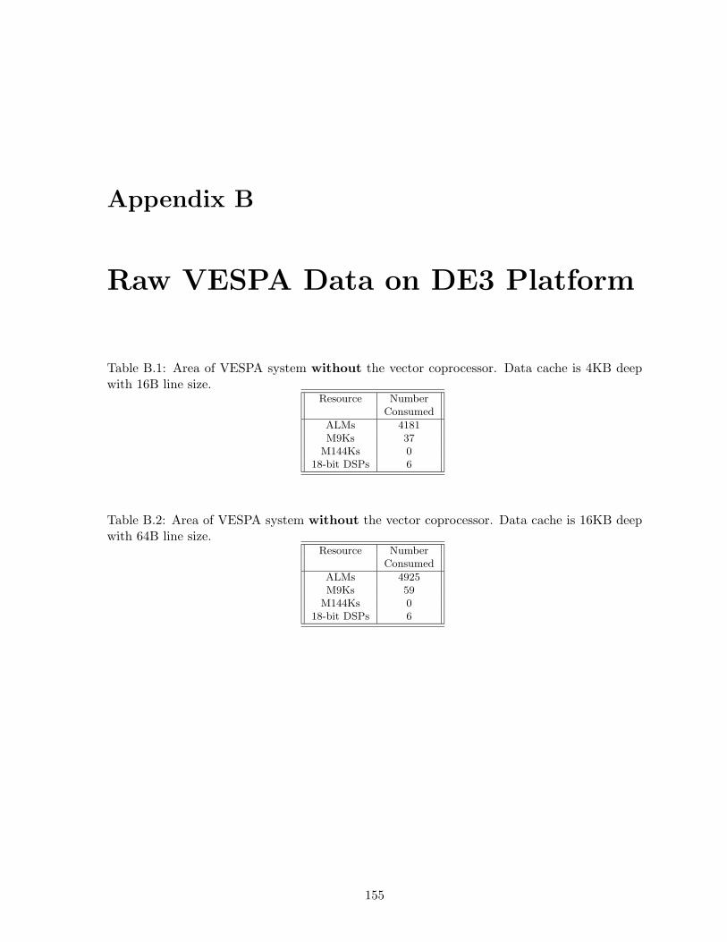
Appendix B
Raw VESPA Data on DE3 Platform
Table B.1: Area of VESPA system without the vector coprocessor. Data cache is 4KB deepwith 16B line size.
Resource NumberConsumed
ALMs 4181M9Ks 37
M144Ks 018-bit DSPs 6
Table B.2: Area of VESPA system without the vector coprocessor. Data cache is 16KB deepwith 64B line size.
Resource NumberConsumed
ALMs 4925M9Ks 59
M144Ks 018-bit DSPs 6
155

Appendix B. Raw VESPA Data on DE3 Platform 156
Table B.3: System area of pareto optimal VESPA configurations.DD DW DPV APB B MVL L M X ALMs M9Ks M144Ks 18-bit
DSPs
8KB 16B 0 0 1 4 1 1 1 5556 46 0 108KB 16B 0 0 1 8 2 1 1 6043 48 0 108KB 16B 0 0 1 8 2 1 2 6075 48 0 148KB 16B 0 0 1 8 2 2 2 6218 48 0 148KB 16B 0 0 2 8 2 2 1 6566 54 0 108KB 16B 0 0 2 8 2 2 2 6591 54 0 148KB 16B 0 0 1 16 4 2 2 7041 52 0 148KB 16B 0 0 1 16 4 2 4 7083 52 0 228KB 16B 0 0 1 16 4 4 2 7216 52 0 148KB 16B 0 0 1 16 4 4 4 7294 52 0 228KB 16B 0 0 2 16 4 4 2 7787 62 0 148KB 16B 0 0 1 128 4 4 4 7362 76 0 228KB 16B 0 0 2 16 4 4 4 8034 62 0 228KB 16B 0 0 2 128 4 4 2 7836 78 0 1432KB 64B 0 0 1 16 4 2 4 8268 74 0 2232KB 64B 8*VL 0 1 16 4 2 4 8261 74 0 238KB 16B 0 0 1 32 8 4 4 8910 60 0 228KB 16B 0 0 2 128 4 4 4 8100 78 0 228KB 16B 0 0 1 32 8 8 4 9278 60 0 2232KB 64B 7 0 1 16 4 4 2 8903 74 0 1432KB 64B 7 0 1 16 4 4 4 9102 74 0 2232KB 64B 7 0 2 16 4 4 2 9525 84 0 1432KB 64B 7 0 2 16 4 4 4 9732 84 0 2232KB 64B 7 0 2 128 4 4 2 9608 100 0 1432KB 64B 8*VL 0 2 128 4 4 2 9670 100 0 1532KB 64B 7 0 2 128 4 4 4 9780 100 0 2232KB 64B 8*VL 0 2 128 4 4 4 9904 100 0 2332KB 64B 8*VL 1 2 128 4 4 4 10458 100 0 2332KB 64B 8*VL 0 1 32 8 8 4 12309 82 0 2332KB 64B 7 0 1 32 8 8 4 12421 82 0 2232KB 64B 7 0 1 32 8 8 8 12458 82 0 3832KB 64B 8*VL 0 1 128 8 8 8 12565 98 0 3932KB 64B 7 0 2 128 8 8 4 13286 100 0 2232KB 64B 8*VL 0 2 128 8 8 4 13383 100 0 2332KB 64B 7 0 2 128 8 8 8 13672 100 0 3832KB 64B 8*VL 0 2 128 8 8 8 14212 100 0 3932KB 64B 7 1 2 128 8 8 8 15008 100 0 3832KB 64B 8*VL 1 2 128 8 8 8 15416 100 0 3932KB 64B 8*VL 0 2 128 16 8 8 17727 132 0 4732KB 64B 8*VL 0 1 64 16 16 8 19598 98 0 4732KB 64B 8*VL 0 1 128 16 16 8 19722 98 0 4732KB 64B 8*VL 0 2 128 16 8 16 18375 132 0 7932KB 64B 8*VL 0 1 64 16 16 16 20179 98 0 7932KB 64B 8*VL 0 1 128 16 16 16 20392 98 0 7932KB 64B 8*VL 0 2 128 16 16 8 21966 132 0 4732KB 64B 7 0 2 128 16 16 16 22716 132 0 7832KB 64B 7 1 2 128 16 16 16 25135 132 0 7832KB 64B 8*VL 1 2 128 16 16 16 25713 132 0 7932KB 64B 7 0 1 128 32 32 32 34489 130 0 17432KB 64B 8*VL 0 2 512 32 16 32 33499 196 0 17532KB 64B 7 0 1 512 32 32 32 34483 196 0 17432KB 64B 8*VL 0 1 512 32 32 32 34471 196 0 17532KB 64B 8*VL 0 2 128 32 32 32 38077 196 0 17532KB 64B 7 0 2 128 32 32 32 38317 196 0 17432KB 64B 8*VL 0 2 512 32 32 32 40097 196 0 17532KB 64B 8*VL 1 2 512 32 32 32 45578 196 0 175
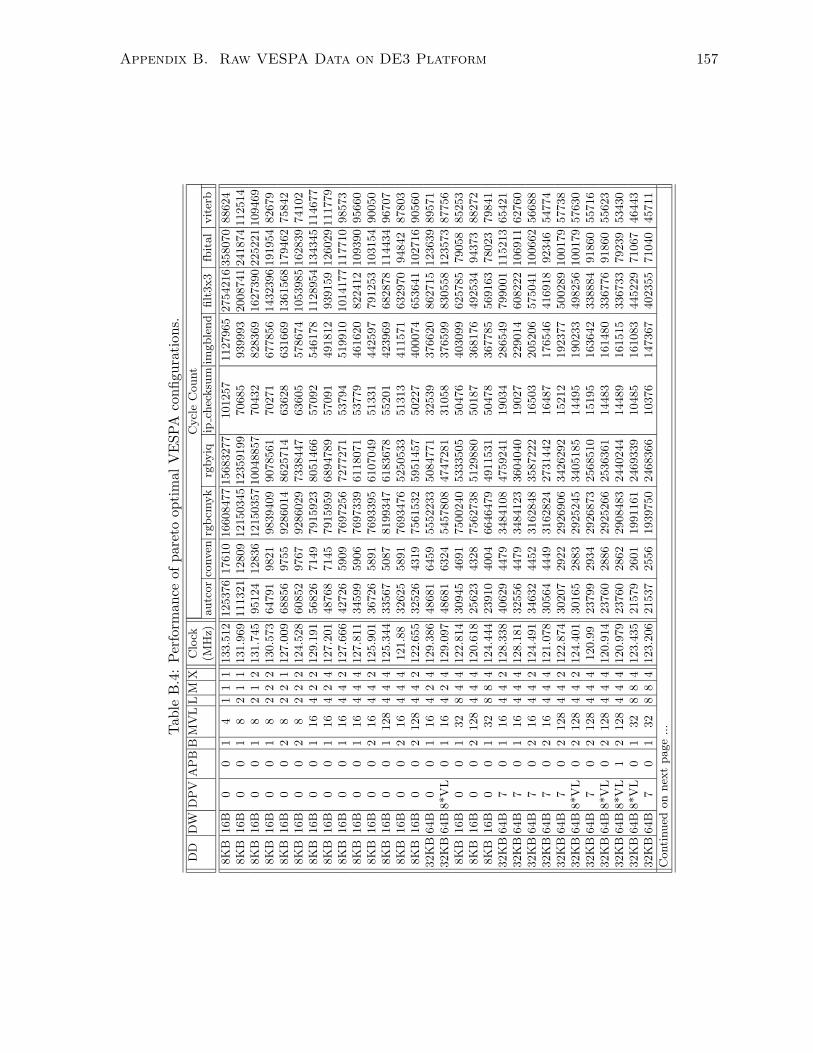
Appendix B. Raw VESPA Data on DE3 Platform 157
Tab
leB
.4:
Per
form
ance
ofpa
reto
opti
mal
VE
SPA
confi
gura
tion
s.D
DD
WD
PV
AP
BB
MV
LL
MX
Clo
ckC
ycl
eC
ount
(MH
z)autc
or
conven
rgbcm
yk
rgbyiq
ipch
ecksu
mim
gble
nd
filt
3x3
fbit
al
vit
erb
8K
B16B
00
14
11
1133.5
12
125376
17610
16608477
15683277
101257
1127965
2754216
358070
88624
8K
B16B
00
18
21
1131.9
69
111321
12809
12150345
12359199
70685
939993
2008741
241874
112514
8K
B16B
00
18
21
2131.7
45
95124
12836
12150357
10048857
70432
828369
1627390
225221
109469
8K
B16B
00
18
22
2130.5
73
64791
9821
9839409
9078561
70271
677856
1432396
191954
82679
8K
B16B
00
28
22
1127.0
09
68856
9755
9286014
8625714
63628
631669
1361568
179462
75842
8K
B16B
00
28
22
2124.5
28
60852
9767
9286029
7338447
63605
578674
1053985
162839
74102
8K
B16B
00
116
42
2129.1
91
56826
7149
7915923
8051466
57092
546178
1128954
134345
114677
8K
B16B
00
116
42
4127.2
01
48768
7145
7915959
6894789
57091
491812
939159
126029
111779
8K
B16B
00
116
44
2127.6
66
42726
5909
7697256
7277271
53794
519910
1014177
117710
98573
8K
B16B
00
116
44
4127.8
11
34599
5906
7697339
6118071
53779
461620
822412
109390
95660
8K
B16B
00
216
44
2125.9
01
36726
5891
7693395
6107049
51331
442597
791253
103154
90050
8K
B16B
00
1128
44
4125.3
44
33567
5087
8199347
6183678
55201
423969
682878
114434
96707
8K
B16B
00
216
44
4121.8
832625
5891
7693476
5250533
51313
411571
632970
94842
87803
8K
B16B
00
2128
44
2122.6
55
32526
4319
7561532
5951457
50227
400074
653641
102716
90560
32K
B64B
00
116
42
4129.3
86
48681
6459
5552233
5084771
32539
376620
862715
123639
89571
32K
B64B
8*V
L0
116
42
4129.0
97
48681
6324
5457808
4747281
31058
376599
830558
123573
87756
8K
B16B
00
132
84
4122.8
14
30945
4691
7500240
5333505
50476
403099
625785
79058
85253
8K
B16B
00
2128
44
4120.6
18
25623
4328
7562738
5129880
50187
368176
492534
94373
88272
8K
B16B
00
132
88
4124.4
44
23910
4004
6646479
4911531
50478
367785
569163
78023
79841
32K
B64B
70
116
44
2128.3
38
40629
4479
3484108
4759241
19034
286549
799001
115213
65421
32K
B64B
70
116
44
4128.1
81
32556
4479
3484123
3604040
19027
229014
608222
106911
62760
32K
B64B
70
216
44
2124.4
91
34632
4452
3162848
3587222
16503
205206
575041
100662
56688
32K
B64B
70
216
44
4121.0
78
30564
4449
3162824
2731442
16487
176546
416918
92346
54774
32K
B64B
70
2128
44
2122.8
74
30207
2922
2926906
3426292
15212
192377
500289
100179
57738
32K
B64B
8*V
L0
2128
44
2124.4
01
30165
2883
2925245
3405185
14495
190233
498256
100179
57630
32K
B64B
70
2128
44
4120.9
923799
2934
2926873
2568510
15195
163642
338884
91860
55716
32K
B64B
8*V
L0
2128
44
4120.9
14
23760
2886
2925266
2536361
14483
161480
336776
91860
55623
32K
B64B
8*V
L1
2128
44
4120.9
79
23760
2862
2908483
2440244
14489
161515
336733
79239
53430
32K
B64B
8*V
L0
132
88
4123.4
35
21579
2601
1991161
2469339
10485
161083
445229
71067
46443
32K
B64B
70
132
88
4123.2
06
21537
2556
1939750
2468366
10376
147367
402355
71040
45711
Conti
nued
on
nex
tpage
...

Appendix B. Raw VESPA Data on DE3 Platform 158
Tab
leB
.5:
Per
form
ance
ofpa
reto
opti
mal
VE
SPA
confi
gura
tion
s(c
ont’
d).
DD
DW
DP
VA
PB
BM
VL
LM
XC
lock
Cycl
eC
ount
(MH
z)autc
orco
nven
rgbcm
yk
rgbyiq
ipch
ecksu
mim
gble
nd
filt
3x3
fbit
alvit
erb
32K
B64B
70
132
88
8125.3
66
17544
2544
1939669
1889822
10384
118704
308331
66882
44885
32K
B64B
8*V
L0
1128
88
8124.2
82
16896
2103
1950742
1844327
10583
112937
271252
69186
44712
32K
B64B
70
2128
88
4116.9
416626
1836
1666588
1794917
8378
101376
258218
63546
43467
32K
B64B
8*V
L0
2128
88
4119.2
75
16599
1809
1649200
1755779
8048
99122
256711
63543
43416
32K
B64B
70
2128
88
8118.3
88
13290
1842
1666540
1365983
8351
87052
177391
59379
42681
32K
B64B
8*V
L0
2128
88
8117.9
13251
1806
1649200
1323693
8029
84761
175766
59388
42582
32K
B64B
71
2128
88
8118.5
57
13281
1827
1661881
1318280
8372
87060
177331
52998
41775
32K
B64B
8*V
L1
2128
88
8119.0
24
13251
1794
1632122
1281143
8048
84776
175745
52998
41691
32K
B64B
8*V
L0
2128
16
88
111.5
56
12897
1701
1471887
1186151
7007
76584
165004
49428
40752
32K
B64B
8*V
L0
164
16
16
8116.4
34
12234
1629
1160999
1286483
6622
78240
193657
49380
38655
32K
B64B
8*V
L0
1128
16
16
8114.1
35
11865
1428
1183943
1324460
6333
76235
189433
50130
38265
32K
B64B
8*V
L0
2128
16
816
110.8
04
11538
1713
1471987
1025345
7111
71424
127225
47358
40338
32K
B64B
8*V
L0
164
16
16
16
113.5
22
10287
1638
1161370
997511
6629
64176
145729
47303
38219
32K
B64B
8*V
L0
1128
16
16
16
115.1
39
9840
1428
1183981
1035968
6356
61842
141815
48054
37845
32K
B64B
8*V
L0
2128
16
16
8108.8
39
10086
1371
1052614
990512
5083
56070
134456
45393
38121
32K
B64B
70
2128
16
16
16
111.3
64
8364
1407
1078405
763593
5850
50232
98573
43323
37830
32K
B64B
71
2128
16
16
16
111.0
95
8355
1401
1065568
742232
5869
53324
98540
40074
37743
32K
B64B
8*V
L1
2128
16
16
16
111.2
08
8337
1368
1035611
756419
5068
48893
94654
40068
37607
32K
B64B
70
1128
32
32
32
96.4
788
6951
1158
803440
604454
5165
39757
82480
38391
37164
32K
B64B
8*V
L0
2512
32
16
32
99.4
55
7722
1140
968581
606074
5896
38828
64750
38784
37392
32K
B64B
70
1512
32
32
32
99.1
338
7095
996
860407
641773
6338
37752
72856
39348
36840
32K
B64B
8*V
L0
1512
32
32
32
98.5
213
7062
984
819688
622727
5708
33953
72966
39372
36879
32K
B64B
8*V
L0
2128
32
32
32
93.7
26718
1143
910417
619962
4026
31614
63493
36513
37095
32K
B64B
70
2128
32
32
32
91.0
025
6744
1153
779770
498854
4582
32909
60284
36513
37149
32K
B64B
8*V
L0
2512
32
32
32
92.4
087
6171
948
746737
492193
5160
27223
49078
36990
36834
32K
B64B
8*V
L1
2512
32
32
32
95.8
025
6177
957
741493
480515
5098
27573
49076
35352
36792

Appendix B. Raw VESPA Data on DE3 Platform 159
Table B.6: System area of pareto optimal VESPA configurations after instruction subsettingand width reduction for autcor.
DD DW DPV APB B MVL L M X ALMs M9Ks M144Ks 18-bitDSPs
8KB 16B 0 0 1 4 1 1 1 5172 46 0 108KB 16B 0 0 1 8 2 1 1 5425 48 0 108KB 16B 0 0 1 8 2 1 2 5379 48 0 148KB 16B 0 0 1 8 2 2 2 5485 48 0 148KB 16B 0 0 2 8 2 2 1 6329 54 0 108KB 16B 0 0 2 8 2 2 2 6440 54 0 148KB 16B 0 0 1 16 4 2 2 5984 52 0 148KB 16B 0 0 1 16 4 2 4 6138 52 0 228KB 16B 0 0 1 16 4 4 2 6063 52 0 148KB 16B 0 0 1 16 4 4 4 6087 52 0 228KB 16B 0 0 2 16 4 4 2 7548 62 0 148KB 16B 0 0 1 128 4 4 4 6197 76 0 228KB 16B 0 0 2 16 4 4 4 7749 62 0 228KB 16B 0 0 2 128 4 4 2 7646 78 0 1432KB 64B 0 0 1 16 4 2 4 6913 74 0 2232KB 64B 8*VL 0 1 16 4 2 4 6916 74 0 228KB 16B 0 0 1 32 8 4 4 7125 60 0 228KB 16B 0 0 2 128 4 4 4 7784 78 0 228KB 16B 0 0 1 32 8 8 4 7319 60 0 2232KB 64B 7 0 1 16 4 4 2 7135 74 0 1432KB 64B 7 0 1 16 4 4 4 7207 74 0 2232KB 64B 7 0 2 16 4 4 2 9371 84 0 1432KB 64B 7 0 2 16 4 4 4 9548 84 0 2232KB 64B 7 0 2 128 4 4 2 9345 100 0 1432KB 64B 8*VL 0 2 128 4 4 2 9397 100 0 1532KB 64B 7 0 2 128 4 4 4 9496 100 0 2232KB 64B 8*VL 0 2 128 4 4 4 9641 100 0 2332KB 64B 8*VL 1 2 128 4 4 4 10233 100 0 2332KB 64B 8*VL 0 1 32 8 8 4 8988 82 0 2232KB 64B 7 0 1 32 8 8 4 9096 82 0 2232KB 64B 7 0 1 32 8 8 8 8956 82 0 3832KB 64B 8*VL 0 1 128 8 8 8 9137 98 0 3832KB 64B 7 0 2 128 8 8 4 13006 100 0 2232KB 64B 8*VL 0 2 128 8 8 4 13007 100 0 2332KB 64B 7 0 2 128 8 8 8 13352 100 0 3832KB 64B 8*VL 0 2 128 8 8 8 13531 100 0 3932KB 64B 7 1 2 128 8 8 8 14572 100 0 3832KB 64B 8*VL 1 2 128 8 8 8 14593 100 0 3932KB 64B 8*VL 0 2 128 16 8 8 17035 132 0 3932KB 64B 8*VL 0 1 64 16 16 8 12456 98 0 3832KB 64B 8*VL 0 1 128 16 16 8 12481 98 0 3832KB 64B 8*VL 0 2 128 16 8 16 17837 132 0 7132KB 64B 8*VL 0 1 64 16 16 16 12779 98 0 7032KB 64B 8*VL 0 1 128 16 16 16 12754 98 0 7032KB 64B 8*VL 0 2 128 16 16 8 22321 132 0 3932KB 64B 7 0 2 128 16 16 16 21901 132 0 7032KB 64B 7 1 2 128 16 16 16 25152 132 0 7032KB 64B 8*VL 1 2 128 16 16 16 24363 132 0 7132KB 64B 7 0 1 128 32 32 32 20555 130 0 13432KB 64B 8*VL 0 2 512 32 16 32 31633 196 0 13532KB 64B 7 0 1 512 32 32 32 20744 196 0 13432KB 64B 8*VL 0 1 512 32 32 32 21034 196 0 13432KB 64B 8*VL 0 2 128 32 32 32 39621 196 0 13532KB 64B 7 0 2 128 32 32 32 36944 196 0 13432KB 64B 8*VL 0 2 512 32 32 32 37234 196 0 13532KB 64B 8*VL 1 2 512 32 32 32 43321 196 0 135

Appendix B. Raw VESPA Data on DE3 Platform 160
Table B.7: System area of pareto optimal VESPA configurations after instruction subsettingand width reduction for conven.
DD DW DPV APB B MVL L M X ALMs M9Ks M144Ks 18-bitDSPs
8KB 16B 0 0 1 4 1 1 1 4900 46 0 68KB 16B 0 0 1 8 2 1 1 4885 46 0 68KB 16B 0 0 1 8 2 1 2 4967 46 0 68KB 16B 0 0 1 8 2 2 2 4952 46 0 68KB 16B 0 0 2 8 2 2 1 5257 50 0 68KB 16B 0 0 2 8 2 2 2 5292 50 0 68KB 16B 0 0 1 16 4 2 2 5135 46 0 68KB 16B 0 0 1 16 4 2 4 5125 46 0 68KB 16B 0 0 1 16 4 4 2 5193 46 0 68KB 16B 0 0 1 16 4 4 4 5243 46 0 68KB 16B 0 0 2 16 4 4 2 5528 50 0 68KB 16B 0 0 1 128 4 4 4 5273 52 0 68KB 16B 0 0 2 16 4 4 4 5607 50 0 68KB 16B 0 0 2 128 4 4 2 5618 54 0 632KB 64B 0 0 1 16 4 2 4 5912 68 0 632KB 64B 8*VL 0 1 16 4 2 4 6007 68 0 78KB 16B 0 0 1 32 8 4 4 5498 48 0 68KB 16B 0 0 2 128 4 4 4 5617 54 0 68KB 16B 0 0 1 32 8 8 4 5494 48 0 632KB 64B 7 0 1 16 4 4 2 6107 68 0 632KB 64B 7 0 1 16 4 4 4 6120 68 0 632KB 64B 7 0 2 16 4 4 2 6458 72 0 632KB 64B 7 0 2 16 4 4 4 6552 72 0 632KB 64B 7 0 2 128 4 4 2 6603 76 0 632KB 64B 8*VL 0 2 128 4 4 2 6586 76 0 732KB 64B 7 0 2 128 4 4 4 6551 76 0 632KB 64B 8*VL 0 2 128 4 4 4 6601 76 0 732KB 64B 8*VL 1 2 128 4 4 4 6606 76 0 732KB 64B 8*VL 0 1 32 8 8 4 6751 70 0 732KB 64B 7 0 1 32 8 8 4 6676 70 0 632KB 64B 7 0 1 32 8 8 8 6737 70 0 632KB 64B 8*VL 0 1 128 8 8 8 6766 74 0 732KB 64B 7 0 2 128 8 8 4 7328 76 0 632KB 64B 8*VL 0 2 128 8 8 4 7355 76 0 732KB 64B 7 0 2 128 8 8 8 7282 76 0 632KB 64B 8*VL 0 2 128 8 8 8 7291 76 0 732KB 64B 7 1 2 128 8 8 8 7419 76 0 632KB 64B 8*VL 1 2 128 8 8 8 7438 76 0 732KB 64B 8*VL 0 2 128 16 8 8 8179 84 0 1532KB 64B 8*VL 0 1 64 16 16 8 8101 74 0 1532KB 64B 8*VL 0 1 128 16 16 8 8054 74 0 1532KB 64B 8*VL 0 2 128 16 8 16 8266 84 0 1532KB 64B 8*VL 0 1 64 16 16 16 8082 74 0 1532KB 64B 8*VL 0 1 128 16 16 16 8103 74 0 1532KB 64B 8*VL 0 2 128 16 16 8 8975 84 0 1532KB 64B 7 0 2 128 16 16 16 8909 84 0 1432KB 64B 7 1 2 128 16 16 16 9173 84 0 1432KB 64B 8*VL 1 2 128 16 16 16 9236 84 0 1532KB 64B 7 0 1 128 32 32 32 11032 82 0 4632KB 64B 8*VL 0 2 512 32 16 32 11146 100 0 4732KB 64B 7 0 1 512 32 32 32 10876 100 0 4632KB 64B 8*VL 0 1 512 32 32 32 10676 100 0 4732KB 64B 8*VL 0 2 128 32 32 32 12470 100 0 4732KB 64B 7 0 2 128 32 32 32 12516 100 0 4632KB 64B 8*VL 0 2 512 32 32 32 12639 100 0 4732KB 64B 8*VL 1 2 512 32 32 32 12863 100 0 47

Appendix B. Raw VESPA Data on DE3 Platform 161
Table B.8: System area of pareto optimal VESPA configurations after instruction subsettingand width reduction for rgbcmyk.
DD DW DPV APB B MVL L M X ALMs M9Ks M144Ks 18-bitDSPs
8KB 16B 0 0 1 4 1 1 1 5072 46 0 68KB 16B 0 0 1 8 2 1 1 5105 46 0 68KB 16B 0 0 1 8 2 1 2 5127 46 0 68KB 16B 0 0 1 8 2 2 2 5264 46 0 68KB 16B 0 0 2 8 2 2 1 5761 50 0 78KB 16B 0 0 2 8 2 2 2 5603 50 0 88KB 16B 0 0 1 16 4 2 2 5413 46 0 68KB 16B 0 0 1 16 4 2 4 5497 46 0 68KB 16B 0 0 1 16 4 4 2 5588 46 0 68KB 16B 0 0 1 16 4 4 4 5656 46 0 68KB 16B 0 0 2 16 4 4 2 6240 50 0 88KB 16B 0 0 1 128 4 4 4 5701 52 0 68KB 16B 0 0 2 16 4 4 4 6296 50 0 108KB 16B 0 0 2 128 4 4 2 6295 54 0 832KB 64B 0 0 1 16 4 2 4 6672 68 0 632KB 64B 8*VL 0 1 16 4 2 4 6660 68 0 78KB 16B 0 0 1 32 8 4 4 5994 48 0 68KB 16B 0 0 2 128 4 4 4 6340 54 0 108KB 16B 0 0 1 32 8 8 4 6469 48 0 632KB 64B 7 0 1 16 4 4 2 7403 68 0 632KB 64B 7 0 1 16 4 4 4 7458 68 0 632KB 64B 7 0 2 16 4 4 2 7878 72 0 832KB 64B 7 0 2 16 4 4 4 7924 72 0 1032KB 64B 7 0 2 128 4 4 2 8018 76 0 832KB 64B 8*VL 0 2 128 4 4 2 8050 76 0 932KB 64B 7 0 2 128 4 4 4 7922 76 0 1032KB 64B 8*VL 0 2 128 4 4 4 8102 76 0 1132KB 64B 8*VL 1 2 128 4 4 4 8241 76 0 1132KB 64B 8*VL 0 1 32 8 8 4 9493 70 0 732KB 64B 7 0 1 32 8 8 4 9434 70 0 632KB 64B 7 0 1 32 8 8 8 9473 70 0 632KB 64B 8*VL 0 1 128 8 8 8 9553 74 0 732KB 64B 7 0 2 128 8 8 4 10754 76 0 1032KB 64B 8*VL 0 2 128 8 8 4 10729 76 0 1132KB 64B 7 0 2 128 8 8 8 10477 76 0 1432KB 64B 8*VL 0 2 128 8 8 8 10670 76 0 1532KB 64B 7 1 2 128 8 8 8 10748 76 0 1432KB 64B 8*VL 1 2 128 8 8 8 11152 76 0 1532KB 64B 8*VL 0 2 128 16 8 8 12005 84 0 2332KB 64B 8*VL 0 1 64 16 16 8 14619 74 0 1532KB 64B 8*VL 0 1 128 16 16 8 14677 74 0 1532KB 64B 8*VL 0 2 128 16 8 16 12064 84 0 3132KB 64B 8*VL 0 1 64 16 16 16 14545 74 0 1532KB 64B 8*VL 0 1 128 16 16 16 14627 74 0 1532KB 64B 8*VL 0 2 128 16 16 8 16942 84 0 2332KB 64B 7 0 2 128 16 16 16 16245 84 0 3032KB 64B 7 1 2 128 16 16 16 16934 84 0 3032KB 64B 8*VL 1 2 128 16 16 16 17635 84 0 3132KB 64B 7 0 1 128 32 32 32 22141 82 0 4632KB 64B 8*VL 0 2 512 32 16 32 20361 100 0 7932KB 64B 7 0 1 512 32 32 32 22012 100 0 4632KB 64B 8*VL 0 1 512 32 32 32 21898 100 0 4732KB 64B 8*VL 0 2 128 32 32 32 27560 100 0 7932KB 64B 7 0 2 128 32 32 32 25509 100 0 7832KB 64B 8*VL 0 2 512 32 32 32 27573 100 0 7932KB 64B 8*VL 1 2 512 32 32 32 28766 100 0 79
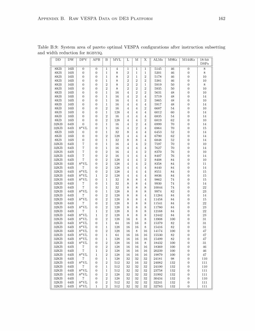
Appendix B. Raw VESPA Data on DE3 Platform 162
Table B.9: System area of pareto optimal VESPA configurations after instruction subsettingand width reduction for rgbyiq.
DD DW DPV APB B MVL L M X ALMs M9Ks M144Ks 18-bitDSPs
8KB 16B 0 0 1 4 1 1 1 5145 46 0 88KB 16B 0 0 1 8 2 1 1 5201 46 0 88KB 16B 0 0 1 8 2 1 2 5178 46 0 108KB 16B 0 0 1 8 2 2 2 5381 46 0 108KB 16B 0 0 2 8 2 2 1 5919 50 0 88KB 16B 0 0 2 8 2 2 2 5935 50 0 108KB 16B 0 0 1 16 4 2 2 5631 48 0 108KB 16B 0 0 1 16 4 2 4 5719 48 0 148KB 16B 0 0 1 16 4 4 2 5865 48 0 108KB 16B 0 0 1 16 4 4 4 5917 48 0 148KB 16B 0 0 2 16 4 4 2 6687 54 0 108KB 16B 0 0 1 128 4 4 4 6012 60 0 148KB 16B 0 0 2 16 4 4 4 6835 54 0 148KB 16B 0 0 2 128 4 4 2 6819 62 0 1032KB 64B 0 0 1 16 4 2 4 6999 70 0 1432KB 64B 8*VL 0 1 16 4 2 4 6964 70 0 158KB 16B 0 0 1 32 8 4 4 6453 52 0 148KB 16B 0 0 2 128 4 4 4 6790 62 0 148KB 16B 0 0 1 32 8 8 4 6848 52 0 1432KB 64B 7 0 1 16 4 4 2 7597 70 0 1032KB 64B 7 0 1 16 4 4 4 7627 70 0 1432KB 64B 7 0 2 16 4 4 2 8370 76 0 1032KB 64B 7 0 2 16 4 4 4 8407 76 0 1432KB 64B 7 0 2 128 4 4 2 8408 84 0 1032KB 64B 8*VL 0 2 128 4 4 2 8358 84 0 1132KB 64B 7 0 2 128 4 4 4 8440 84 0 1432KB 64B 8*VL 0 2 128 4 4 4 8551 84 0 1532KB 64B 8*VL 1 2 128 4 4 4 8836 84 0 1532KB 64B 8*VL 0 1 32 8 8 4 9862 74 0 1532KB 64B 7 0 1 32 8 8 4 9930 74 0 1432KB 64B 7 0 1 32 8 8 8 10044 74 0 2232KB 64B 8*VL 0 1 128 8 8 8 9974 82 0 2332KB 64B 7 0 2 128 8 8 4 11284 84 0 1432KB 64B 8*VL 0 2 128 8 8 4 11458 84 0 1532KB 64B 7 0 2 128 8 8 8 11541 84 0 2232KB 64B 8*VL 0 2 128 8 8 8 11780 84 0 2332KB 64B 7 1 2 128 8 8 8 12168 84 0 2232KB 64B 8*VL 1 2 128 8 8 8 12442 84 0 2332KB 64B 8*VL 0 2 128 16 8 8 13908 100 0 3132KB 64B 8*VL 0 1 64 16 16 8 15379 82 0 3132KB 64B 8*VL 0 1 128 16 16 8 15416 82 0 3132KB 64B 8*VL 0 2 128 16 8 16 14174 100 0 4732KB 64B 8*VL 0 1 64 16 16 16 15530 82 0 4732KB 64B 8*VL 0 1 128 16 16 16 15499 82 0 4732KB 64B 8*VL 0 2 128 16 16 8 18432 100 0 3132KB 64B 7 0 2 128 16 16 16 18369 100 0 4632KB 64B 7 1 2 128 16 16 16 20239 100 0 4632KB 64B 8*VL 1 2 128 16 16 16 19879 100 0 4732KB 64B 7 0 1 128 32 32 32 24181 98 0 11032KB 64B 8*VL 0 2 512 32 16 32 24082 132 0 11132KB 64B 7 0 1 512 32 32 32 24100 132 0 11032KB 64B 8*VL 0 1 512 32 32 32 23758 132 0 11132KB 64B 8*VL 0 2 128 32 32 32 31992 132 0 11132KB 64B 7 0 2 128 32 32 32 30434 132 0 11032KB 64B 8*VL 0 2 512 32 32 32 32241 132 0 11132KB 64B 8*VL 1 2 512 32 32 32 32783 132 0 111
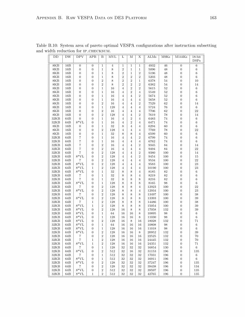
Appendix B. Raw VESPA Data on DE3 Platform 163
Table B.10: System area of pareto optimal VESPA configurations after instruction subsettingand width reduction for ip checksum.
DD DW DPV APB B MVL L M X ALMs M9Ks M144Ks 18-bitDSPs
8KB 16B 0 0 1 4 1 1 1 4932 46 0 68KB 16B 0 0 1 8 2 1 1 5096 48 0 68KB 16B 0 0 1 8 2 1 2 5196 48 0 68KB 16B 0 0 1 8 2 2 2 5203 48 0 68KB 16B 0 0 2 8 2 2 1 6378 54 0 108KB 16B 0 0 2 8 2 2 2 6382 54 0 148KB 16B 0 0 1 16 4 2 2 5615 52 0 68KB 16B 0 0 1 16 4 2 4 5549 52 0 68KB 16B 0 0 1 16 4 4 2 5674 52 0 68KB 16B 0 0 1 16 4 4 4 5658 52 0 68KB 16B 0 0 2 16 4 4 2 7529 62 0 148KB 16B 0 0 1 128 4 4 4 5724 76 0 68KB 16B 0 0 2 16 4 4 4 7706 62 0 228KB 16B 0 0 2 128 4 4 2 7619 78 0 1432KB 64B 0 0 1 16 4 2 4 6483 74 0 632KB 64B 8*VL 0 1 16 4 2 4 6471 74 0 68KB 16B 0 0 1 32 8 4 4 6294 60 0 68KB 16B 0 0 2 128 4 4 4 7769 78 0 228KB 16B 0 0 1 32 8 8 4 6599 60 0 632KB 64B 7 0 1 16 4 4 2 6799 74 0 632KB 64B 7 0 1 16 4 4 4 6762 74 0 632KB 64B 7 0 2 16 4 4 2 9345 84 0 1432KB 64B 7 0 2 16 4 4 4 9494 84 0 2232KB 64B 7 0 2 128 4 4 2 9380 100 0 1432KB 64B 8*VL 0 2 128 4 4 2 9454 100 0 1532KB 64B 7 0 2 128 4 4 4 9534 100 0 2232KB 64B 8*VL 0 2 128 4 4 4 9583 100 0 2332KB 64B 8*VL 1 2 128 4 4 4 10190 100 0 2332KB 64B 8*VL 0 1 32 8 8 4 8185 82 0 632KB 64B 7 0 1 32 8 8 4 8219 82 0 632KB 64B 7 0 1 32 8 8 8 8216 82 0 632KB 64B 8*VL 0 1 128 8 8 8 8165 98 0 632KB 64B 7 0 2 128 8 8 4 12923 100 0 2232KB 64B 8*VL 0 2 128 8 8 4 12934 100 0 2332KB 64B 7 0 2 128 8 8 8 13497 100 0 3832KB 64B 8*VL 0 2 128 8 8 8 13393 100 0 3932KB 64B 7 1 2 128 8 8 8 14486 100 0 3832KB 64B 8*VL 1 2 128 8 8 8 15054 100 0 3932KB 64B 8*VL 0 2 128 16 8 8 17058 132 0 3932KB 64B 8*VL 0 1 64 16 16 8 10895 98 0 632KB 64B 8*VL 0 1 128 16 16 8 11030 98 0 632KB 64B 8*VL 0 2 128 16 8 16 18028 132 0 7132KB 64B 8*VL 0 1 64 16 16 16 10808 98 0 632KB 64B 8*VL 0 1 128 16 16 16 11018 98 0 632KB 64B 8*VL 0 2 128 16 16 8 20952 132 0 3932KB 64B 7 0 2 128 16 16 16 22525 132 0 7032KB 64B 7 1 2 128 16 16 16 24445 132 0 7032KB 64B 8*VL 1 2 128 16 16 16 24351 132 0 7132KB 64B 7 0 1 128 32 32 32 16854 130 0 632KB 64B 8*VL 0 2 512 32 16 32 31153 196 0 13532KB 64B 7 0 1 512 32 32 32 17031 196 0 632KB 64B 8*VL 0 1 512 32 32 32 16911 196 0 632KB 64B 8*VL 0 2 128 32 32 32 37247 196 0 13532KB 64B 7 0 2 128 32 32 32 39438 196 0 13432KB 64B 8*VL 0 2 512 32 32 32 39597 196 0 13532KB 64B 8*VL 1 2 512 32 32 32 42765 196 0 135
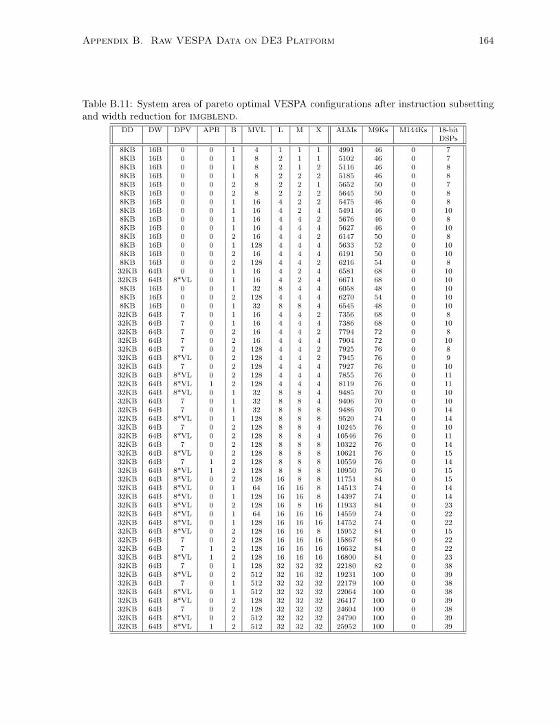
Appendix B. Raw VESPA Data on DE3 Platform 164
Table B.11: System area of pareto optimal VESPA configurations after instruction subsettingand width reduction for imgblend.
DD DW DPV APB B MVL L M X ALMs M9Ks M144Ks 18-bitDSPs
8KB 16B 0 0 1 4 1 1 1 4991 46 0 78KB 16B 0 0 1 8 2 1 1 5102 46 0 78KB 16B 0 0 1 8 2 1 2 5116 46 0 88KB 16B 0 0 1 8 2 2 2 5185 46 0 88KB 16B 0 0 2 8 2 2 1 5652 50 0 78KB 16B 0 0 2 8 2 2 2 5645 50 0 88KB 16B 0 0 1 16 4 2 2 5475 46 0 88KB 16B 0 0 1 16 4 2 4 5491 46 0 108KB 16B 0 0 1 16 4 4 2 5676 46 0 88KB 16B 0 0 1 16 4 4 4 5627 46 0 108KB 16B 0 0 2 16 4 4 2 6147 50 0 88KB 16B 0 0 1 128 4 4 4 5633 52 0 108KB 16B 0 0 2 16 4 4 4 6191 50 0 108KB 16B 0 0 2 128 4 4 2 6216 54 0 832KB 64B 0 0 1 16 4 2 4 6581 68 0 1032KB 64B 8*VL 0 1 16 4 2 4 6671 68 0 108KB 16B 0 0 1 32 8 4 4 6058 48 0 108KB 16B 0 0 2 128 4 4 4 6270 54 0 108KB 16B 0 0 1 32 8 8 4 6545 48 0 1032KB 64B 7 0 1 16 4 4 2 7356 68 0 832KB 64B 7 0 1 16 4 4 4 7386 68 0 1032KB 64B 7 0 2 16 4 4 2 7794 72 0 832KB 64B 7 0 2 16 4 4 4 7904 72 0 1032KB 64B 7 0 2 128 4 4 2 7925 76 0 832KB 64B 8*VL 0 2 128 4 4 2 7945 76 0 932KB 64B 7 0 2 128 4 4 4 7927 76 0 1032KB 64B 8*VL 0 2 128 4 4 4 7855 76 0 1132KB 64B 8*VL 1 2 128 4 4 4 8119 76 0 1132KB 64B 8*VL 0 1 32 8 8 4 9485 70 0 1032KB 64B 7 0 1 32 8 8 4 9406 70 0 1032KB 64B 7 0 1 32 8 8 8 9486 70 0 1432KB 64B 8*VL 0 1 128 8 8 8 9520 74 0 1432KB 64B 7 0 2 128 8 8 4 10245 76 0 1032KB 64B 8*VL 0 2 128 8 8 4 10546 76 0 1132KB 64B 7 0 2 128 8 8 8 10322 76 0 1432KB 64B 8*VL 0 2 128 8 8 8 10621 76 0 1532KB 64B 7 1 2 128 8 8 8 10559 76 0 1432KB 64B 8*VL 1 2 128 8 8 8 10950 76 0 1532KB 64B 8*VL 0 2 128 16 8 8 11751 84 0 1532KB 64B 8*VL 0 1 64 16 16 8 14513 74 0 1432KB 64B 8*VL 0 1 128 16 16 8 14397 74 0 1432KB 64B 8*VL 0 2 128 16 8 16 11933 84 0 2332KB 64B 8*VL 0 1 64 16 16 16 14559 74 0 2232KB 64B 8*VL 0 1 128 16 16 16 14752 74 0 2232KB 64B 8*VL 0 2 128 16 16 8 15952 84 0 1532KB 64B 7 0 2 128 16 16 16 15867 84 0 2232KB 64B 7 1 2 128 16 16 16 16632 84 0 2232KB 64B 8*VL 1 2 128 16 16 16 16800 84 0 2332KB 64B 7 0 1 128 32 32 32 22180 82 0 3832KB 64B 8*VL 0 2 512 32 16 32 19231 100 0 3932KB 64B 7 0 1 512 32 32 32 22179 100 0 3832KB 64B 8*VL 0 1 512 32 32 32 22064 100 0 3832KB 64B 8*VL 0 2 128 32 32 32 26417 100 0 3932KB 64B 7 0 2 128 32 32 32 24604 100 0 3832KB 64B 8*VL 0 2 512 32 32 32 24790 100 0 3932KB 64B 8*VL 1 2 512 32 32 32 25952 100 0 39

Appendix B. Raw VESPA Data on DE3 Platform 165
Table B.12: System area of pareto optimal VESPA configurations after instruction subsettingand width reduction for filt3x3.
DD DW DPV APB B MVL L M X ALMs M9Ks M144Ks 18-bitDSPs
8KB 16B 0 0 1 4 1 1 1 4991 46 0 78KB 16B 0 0 1 8 2 1 1 5102 46 0 78KB 16B 0 0 1 8 2 1 2 5116 46 0 88KB 16B 0 0 1 8 2 2 2 5185 46 0 88KB 16B 0 0 2 8 2 2 1 5652 50 0 78KB 16B 0 0 2 8 2 2 2 5645 50 0 88KB 16B 0 0 1 16 4 2 2 5475 46 0 88KB 16B 0 0 1 16 4 2 4 5491 46 0 108KB 16B 0 0 1 16 4 4 2 5676 46 0 88KB 16B 0 0 1 16 4 4 4 5627 46 0 108KB 16B 0 0 2 16 4 4 2 6147 50 0 88KB 16B 0 0 1 128 4 4 4 5633 52 0 108KB 16B 0 0 2 16 4 4 4 6191 50 0 108KB 16B 0 0 2 128 4 4 2 6216 54 0 832KB 64B 0 0 1 16 4 2 4 6581 68 0 1032KB 64B 8*VL 0 1 16 4 2 4 6671 68 0 108KB 16B 0 0 1 32 8 4 4 6058 48 0 108KB 16B 0 0 2 128 4 4 4 6270 54 0 108KB 16B 0 0 1 32 8 8 4 6545 48 0 1032KB 64B 7 0 1 16 4 4 2 7356 68 0 832KB 64B 7 0 1 16 4 4 4 7386 68 0 1032KB 64B 7 0 2 16 4 4 2 7794 72 0 832KB 64B 7 0 2 16 4 4 4 7904 72 0 1032KB 64B 7 0 2 128 4 4 2 7925 76 0 832KB 64B 8*VL 0 2 128 4 4 2 7945 76 0 932KB 64B 7 0 2 128 4 4 4 7927 76 0 1032KB 64B 8*VL 0 2 128 4 4 4 7855 76 0 1132KB 64B 8*VL 1 2 128 4 4 4 8119 76 0 1132KB 64B 8*VL 0 1 32 8 8 4 9485 70 0 1032KB 64B 7 0 1 32 8 8 4 9406 70 0 1032KB 64B 7 0 1 32 8 8 8 9486 70 0 1432KB 64B 8*VL 0 1 128 8 8 8 9520 74 0 1432KB 64B 7 0 2 128 8 8 4 10245 76 0 1032KB 64B 8*VL 0 2 128 8 8 4 10546 76 0 1132KB 64B 7 0 2 128 8 8 8 10322 76 0 1432KB 64B 8*VL 0 2 128 8 8 8 10621 76 0 1532KB 64B 7 1 2 128 8 8 8 10559 76 0 1432KB 64B 8*VL 1 2 128 8 8 8 10950 76 0 1532KB 64B 8*VL 0 2 128 16 8 8 11751 84 0 1532KB 64B 8*VL 0 1 64 16 16 8 14513 74 0 1432KB 64B 8*VL 0 1 128 16 16 8 14397 74 0 1432KB 64B 8*VL 0 2 128 16 8 16 11933 84 0 2332KB 64B 8*VL 0 1 64 16 16 16 14559 74 0 2232KB 64B 8*VL 0 1 128 16 16 16 14752 74 0 2232KB 64B 8*VL 0 2 128 16 16 8 15952 84 0 1532KB 64B 7 0 2 128 16 16 16 15867 84 0 2232KB 64B 7 1 2 128 16 16 16 16632 84 0 2232KB 64B 8*VL 1 2 128 16 16 16 16800 84 0 2332KB 64B 7 0 1 128 32 32 32 22180 82 0 3832KB 64B 8*VL 0 2 512 32 16 32 19231 100 0 3932KB 64B 7 0 1 512 32 32 32 22179 100 0 3832KB 64B 8*VL 0 1 512 32 32 32 22064 100 0 3832KB 64B 8*VL 0 2 128 32 32 32 26417 100 0 3932KB 64B 7 0 2 128 32 32 32 24604 100 0 3832KB 64B 8*VL 0 2 512 32 32 32 24790 100 0 3932KB 64B 8*VL 1 2 512 32 32 32 25952 100 0 39
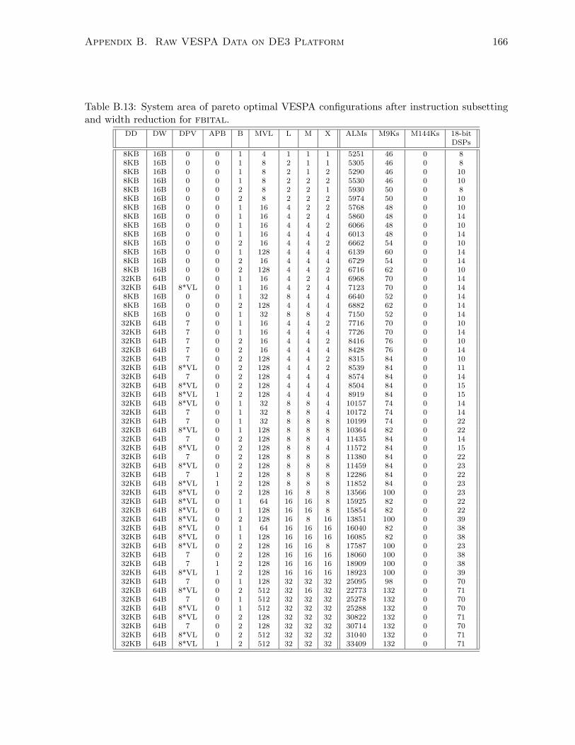
Appendix B. Raw VESPA Data on DE3 Platform 166
Table B.13: System area of pareto optimal VESPA configurations after instruction subsettingand width reduction for fbital.
DD DW DPV APB B MVL L M X ALMs M9Ks M144Ks 18-bitDSPs
8KB 16B 0 0 1 4 1 1 1 5251 46 0 88KB 16B 0 0 1 8 2 1 1 5305 46 0 88KB 16B 0 0 1 8 2 1 2 5290 46 0 108KB 16B 0 0 1 8 2 2 2 5530 46 0 108KB 16B 0 0 2 8 2 2 1 5930 50 0 88KB 16B 0 0 2 8 2 2 2 5974 50 0 108KB 16B 0 0 1 16 4 2 2 5768 48 0 108KB 16B 0 0 1 16 4 2 4 5860 48 0 148KB 16B 0 0 1 16 4 4 2 6066 48 0 108KB 16B 0 0 1 16 4 4 4 6013 48 0 148KB 16B 0 0 2 16 4 4 2 6662 54 0 108KB 16B 0 0 1 128 4 4 4 6139 60 0 148KB 16B 0 0 2 16 4 4 4 6729 54 0 148KB 16B 0 0 2 128 4 4 2 6716 62 0 1032KB 64B 0 0 1 16 4 2 4 6968 70 0 1432KB 64B 8*VL 0 1 16 4 2 4 7123 70 0 148KB 16B 0 0 1 32 8 4 4 6640 52 0 148KB 16B 0 0 2 128 4 4 4 6882 62 0 148KB 16B 0 0 1 32 8 8 4 7150 52 0 1432KB 64B 7 0 1 16 4 4 2 7716 70 0 1032KB 64B 7 0 1 16 4 4 4 7726 70 0 1432KB 64B 7 0 2 16 4 4 2 8416 76 0 1032KB 64B 7 0 2 16 4 4 4 8428 76 0 1432KB 64B 7 0 2 128 4 4 2 8315 84 0 1032KB 64B 8*VL 0 2 128 4 4 2 8539 84 0 1132KB 64B 7 0 2 128 4 4 4 8574 84 0 1432KB 64B 8*VL 0 2 128 4 4 4 8504 84 0 1532KB 64B 8*VL 1 2 128 4 4 4 8919 84 0 1532KB 64B 8*VL 0 1 32 8 8 4 10157 74 0 1432KB 64B 7 0 1 32 8 8 4 10172 74 0 1432KB 64B 7 0 1 32 8 8 8 10199 74 0 2232KB 64B 8*VL 0 1 128 8 8 8 10364 82 0 2232KB 64B 7 0 2 128 8 8 4 11435 84 0 1432KB 64B 8*VL 0 2 128 8 8 4 11572 84 0 1532KB 64B 7 0 2 128 8 8 8 11380 84 0 2232KB 64B 8*VL 0 2 128 8 8 8 11459 84 0 2332KB 64B 7 1 2 128 8 8 8 12286 84 0 2232KB 64B 8*VL 1 2 128 8 8 8 11852 84 0 2332KB 64B 8*VL 0 2 128 16 8 8 13566 100 0 2332KB 64B 8*VL 0 1 64 16 16 8 15925 82 0 2232KB 64B 8*VL 0 1 128 16 16 8 15854 82 0 2232KB 64B 8*VL 0 2 128 16 8 16 13851 100 0 3932KB 64B 8*VL 0 1 64 16 16 16 16040 82 0 3832KB 64B 8*VL 0 1 128 16 16 16 16085 82 0 3832KB 64B 8*VL 0 2 128 16 16 8 17587 100 0 2332KB 64B 7 0 2 128 16 16 16 18060 100 0 3832KB 64B 7 1 2 128 16 16 16 18909 100 0 3832KB 64B 8*VL 1 2 128 16 16 16 18923 100 0 3932KB 64B 7 0 1 128 32 32 32 25095 98 0 7032KB 64B 8*VL 0 2 512 32 16 32 22773 132 0 7132KB 64B 7 0 1 512 32 32 32 25278 132 0 7032KB 64B 8*VL 0 1 512 32 32 32 25288 132 0 7032KB 64B 8*VL 0 2 128 32 32 32 30822 132 0 7132KB 64B 7 0 2 128 32 32 32 30714 132 0 7032KB 64B 8*VL 0 2 512 32 32 32 31040 132 0 7132KB 64B 8*VL 1 2 512 32 32 32 33409 132 0 71

Appendix B. Raw VESPA Data on DE3 Platform 167
Table B.14: System area of pareto optimal VESPA configurations after instruction subsettingand width reduction for viterb.
DD DW DPV APB B MVL L M X ALMs M9Ks M144Ks 18-bitDSPs
8KB 16B 0 0 1 4 1 1 1 5149 46 0 88KB 16B 0 0 1 8 2 1 1 5314 46 0 88KB 16B 0 0 1 8 2 1 2 5377 46 0 108KB 16B 0 0 1 8 2 2 2 5416 46 0 108KB 16B 0 0 2 8 2 2 1 5903 50 0 88KB 16B 0 0 2 8 2 2 2 5885 50 0 108KB 16B 0 0 1 16 4 2 2 5750 48 0 108KB 16B 0 0 1 16 4 2 4 5833 48 0 148KB 16B 0 0 1 16 4 4 2 6005 48 0 108KB 16B 0 0 1 16 4 4 4 6088 48 0 148KB 16B 0 0 2 16 4 4 2 6714 54 0 108KB 16B 0 0 1 128 4 4 4 6126 60 0 148KB 16B 0 0 2 16 4 4 4 6767 54 0 148KB 16B 0 0 2 128 4 4 2 6805 62 0 1032KB 64B 0 0 1 16 4 2 4 7078 70 0 1432KB 64B 8*VL 0 1 16 4 2 4 6908 70 0 158KB 16B 0 0 1 32 8 4 4 6656 52 0 148KB 16B 0 0 2 128 4 4 4 6849 62 0 148KB 16B 0 0 1 32 8 8 4 7231 52 0 1432KB 64B 7 0 1 16 4 4 2 7733 70 0 1032KB 64B 7 0 1 16 4 4 4 7769 70 0 1432KB 64B 7 0 2 16 4 4 2 8404 76 0 1032KB 64B 7 0 2 16 4 4 4 8446 76 0 1432KB 64B 7 0 2 128 4 4 2 8510 84 0 1032KB 64B 8*VL 0 2 128 4 4 2 8350 84 0 1132KB 64B 7 0 2 128 4 4 4 8504 84 0 1432KB 64B 8*VL 0 2 128 4 4 4 8478 84 0 1532KB 64B 8*VL 1 2 128 4 4 4 8881 84 0 1532KB 64B 8*VL 0 1 32 8 8 4 10142 74 0 1532KB 64B 7 0 1 32 8 8 4 10151 74 0 1432KB 64B 7 0 1 32 8 8 8 10095 74 0 2232KB 64B 8*VL 0 1 128 8 8 8 10271 82 0 2332KB 64B 7 0 2 128 8 8 4 11447 84 0 1432KB 64B 8*VL 0 2 128 8 8 4 11358 84 0 1532KB 64B 7 0 2 128 8 8 8 11422 84 0 2232KB 64B 8*VL 0 2 128 8 8 8 11695 84 0 2332KB 64B 7 1 2 128 8 8 8 11964 84 0 2232KB 64B 8*VL 1 2 128 8 8 8 12296 84 0 2332KB 64B 8*VL 0 2 128 16 8 8 13867 100 0 3132KB 64B 8*VL 0 1 64 16 16 8 15784 82 0 3132KB 64B 8*VL 0 1 128 16 16 8 15814 82 0 3132KB 64B 8*VL 0 2 128 16 8 16 14167 100 0 4732KB 64B 8*VL 0 1 64 16 16 16 16119 82 0 4732KB 64B 8*VL 0 1 128 16 16 16 16032 82 0 4732KB 64B 8*VL 0 2 128 16 16 8 17666 100 0 3132KB 64B 7 0 2 128 16 16 16 17966 100 0 4632KB 64B 7 1 2 128 16 16 16 19147 100 0 4632KB 64B 8*VL 1 2 128 16 16 16 19982 100 0 4732KB 64B 7 0 1 128 32 32 32 24991 98 0 11032KB 64B 8*VL 0 2 512 32 16 32 23890 132 0 11132KB 64B 7 0 1 512 32 32 32 25096 132 0 11032KB 64B 8*VL 0 1 512 32 32 32 25891 132 0 11132KB 64B 8*VL 0 2 128 32 32 32 31784 132 0 11132KB 64B 7 0 2 128 32 32 32 31810 132 0 11032KB 64B 8*VL 0 2 512 32 32 32 32233 132 0 11132KB 64B 8*VL 1 2 512 32 32 32 34351 132 0 111
Appendix C
Instruction Disabling Using Verilog
Instruction subsetting is supported by automatically disabling instructions directly in
Verilog as opposed to building higher-level tools that generate the Verilog of the subsetted
processor. In this appendix we briefly describe the mechanism for enabling this in Verilog.
Similar to C, Verilog supports case statements which compare multiple values to a
single variable and perform the operations associated with the value that matches the
current value of the variable. Verilog also supports two special non-integer values: z for
high-impedance values and x for unknown values. To support the desired matching or
ignoring of these special values (treat as don’t care), three case statement variants exist.
1. case – Matches both z and x
2. casez – Don’t care for z, matches x
3. casex – Don’t care for both z and x
A real hardware circuit can never produce the value x–it is symbolic. Therefore any
requests to match x will be optimized away by the FPGA synthesis tools. We can use
this behaviour to eliminate hardware for a given instruction as described below using
Listing C.1 as an example.
First, use a case or casez statement to examine the current instruction opcode and
compare it against the different opcode values. Then, each instruction should enable key
168

Appendix C. Instruction Disabling Using Verilog 169
Listing C.1: Example Verilog case statement for decoding instructions and accompanying mul-tiplexer for selecting results between adder and multiplier.
parameter OP ADD=’ h3f5parameter OP MUL=’ h3c7
always@∗begin
s e l =0;case ( i n s t r opcode )
OP ADD: s e l =0;OP MUL: s e l =1;
endcaseend
a s s i gn r e s u l t= ( s e l ) ? mu l r e su l t : add r e su l t ;
control signals upon being matched with the current instruction. In the example shown
a multiplexer selects the result from either the adder or multiplier functional units and
makes this selection based on the current opcode. To disable the multiply instruction
a user need only insert a single x into its opcode value. In the example shown we can
change ’h3c7 to ’hxxx. As a result of this, the synthesis tools will recognize that the value
OP MUL can never match the current opcode and ignore any signals being set within the
OP MUL case statement clause. The synthesis tool will then discern that the multiplexer
sel signal is never set to 1 and will eliminate that input to the multiplexer as well as
the multiplier feeding it since it longer has any fan-out.
The reader should notice that the reason the sel signal never takes the value 1
after disabling the multiply is because its default assignment is set to 0 as seen in the
sel=0 statement beneath the begin keyword. This illuminates a key consideration for
performing instruction subsetting using this method: default values of control signals
should be assigned to match the values of the instructions that are least likely to be
subsetted in any application and/or least costly to support in hardware. In the example
above, the sel signal is set to 0 by default to match the add instruction. Addition
instructions are more likely to be used within an application than a multiply. They
are also much cheaper to implement in the FPGA fabric. With this default setting, the
hardware for supporting add instructions could never be fully eliminated by the synthesis
Appendix C. Instruction Disabling Using Verilog 170
tool, however since this is unlikely to occur and would only save a moderate amount of
area we accept this limitation. VESPA has this same limitation for adds as well as
loads. The only way to fully eliminate the hardware associated for these instructions is
to eliminate the complete coprocessor.
Bibliography
[1] “Intelligent ram (iram): the industrial setting, applications, and architectures,” in
ICCD ’97: Proceedings of the 1997 International Conference on Computer Design
(ICCD ’97). Washington, DC, USA: IEEE Computer Society, 1997, p. 2.
[2] “Actel ARM Cortex-M1,” http://www.actel.com/products/mpu/cortexm1/default.aspx,
Actel Corporation.
[3] T. Allen, “Altera Corporation,” Private Communication, 2009.
[4] “Excalibur,” http://www.altera.com/products/devices/arm/arm-index.html, Al-
tera.
[5] “Nios II,” http://www.altera.com/products/ip/processors/nios2, Altera.
[6] K. Asanovic, J. Beck, B. Irissou, B. Kingsbury, and N. Morgan, “The TO Vector
Microprocessor,” Hot Chips, vol. 7, pp. 187–196, 1995.
[7] K. Asanovic, “Vector Microprocessors,” Ph.D. dissertation, University of California-
Berkeley, 1998.
[8] J. Ball, “Altera Corporation,” Private Communication, 2005.
[9] ——, “Altera Corporation,” Private Communication, 2009.
[10] D. Besedin, “Platform benchmarking with RightMark memory analyzer,”
http://www.digit-life.com, 2004.
171
BIBLIOGRAPHY 172
[11] M. Budiu and S. C. Goldstein, “Bitvalue inference: Detecting and exploiting narrow
bitwidth computations,” in In Proceedings of the EuroPar 2000 European Conference
on Parallel Computing. Springer Verlag, 2000, pp. 969–979.
[12] R. Carli, “Flexible MIPS Soft Processor Architecture,” Massachusetts Institute
of Technology, Tech. Rep. MIT-CSAIL-TR-2008-036, 2008. [Online]. Available:
http://hdl.handle.net/1721.1/41874
[13] R. Cliff, “Altera Corporation,” Private Communication, 2005.
[14] G. C. Collections, “Auto-vectorization in GCC,” http://gcc.gnu.org/projects/tree-
ssa/vectorization.html, 2009.
[15] R. Dimond, O. Mencer, and W. Luk, “Application-specific customisation of multi-
threaded soft processors,” Computers and Digital Techniques, IEE Proceedings -,
vol. 153, no. 3, pp. 173–180, May 2006.
[16] ——, “ CUSTARD - A Customisable Threaded FPGA Soft Processor and Tools ,”
in International Conference on Field Programmable Logic (FPL), August 2005.
[17] B. A. Draper, A. P. W. Bohm, J. Hammes, W. A. Najjar, J. R. Beveridge, C. Ross,
M. Chawathe, M. Desai, and J. Bins, “Compiling sa-c programs to fpgas: Perfor-
mance results,” in ICVS ’01: Proceedings of the Second International Workshop on
Computer Vision Systems. London, UK: Springer-Verlag, 2001, pp. 220–235.
[18] “The Embedded Microprocessor Benchmark Consortium,” http://www.eembc.org,
EEMBC.
[19] J. Fender, J. Rose, and D. R. Galloway, “The transmogrifier-4: An fpga-based
hardware development system with multi-gigabyte memory capacity and high host
and memory bandwidth.” in IEEE International Conference on Field Programmable
Technology, 2005, pp. 301–302.

BIBLIOGRAPHY 173
[20] M. Flynn and P. Hung, “Microprocessor design issues: thoughts on the road ahead,”
Micro, IEEE, vol. 25, no. 3, pp. 16–31, May-June 2005.
[21] B. Fort, D. Capalija, Z. G. Vranesic, and S. D. Brown, “A multithreaded soft pro-
cessor for sopc area reduction,” in FCCM ’06: Proceedings of the 14th Annual IEEE
Symposium on Field-Programmable Custom Computing Machines. Washington,
DC, USA: IEEE Computer Society, 2006, pp. 131–142.
[22] J. W. C. Fu and J. H. Patel, “Data prefetching in multiprocessor vector cache
memories,” SIGARCH Comput. Archit. News, vol. 19, no. 3, pp. 54–63, 1991.
[23] “LEON SPARC,” http://www.gaisler.com, Gaisler Research.
[24] J. Gebis and D. Patterson, “Embracing and Extending 20th-Century Instruction Set
Architectures,” Computer, vol. 40, no. 4, pp. 68–75, 2007.
[25] M. B. Gokhale, J. M. Stone, J. Arnold, and M. Kalinowski, “Stream-oriented fpga
computing in the streams-c high level language,” in FCCM ’00: Proceedings of
the 2000 IEEE Symposium on Field-Programmable Custom Computing Machines.
Washington, DC, USA: IEEE Computer Society, 2000. [Online]. Available:
http://portal.acm.org/citation.cfm?id=795916
[26] J. Gray, “Designing a simple fpga-optimized risc cpu and system-on-a-chip,” 2000.
[Online]. Available: citeseer.ist.psu.edu/article/gray00designing.html
[27] Z. Guo, W. Najjar, F. Vahid, and K. Vissers, “A quantitative analysis of the speedup
factors of fpgas over processors,” in Symposium on Field programmable gate arrays.
New York, NY, USA: ACM, 2004, pp. 162–170.
[28] J. L. Hennessy and D. A. Patterson, Computer Architecture; A Quantitative Ap-
proach. San Francisco, CA, USA: Morgan Kaufmann Publishers Inc., 1992.
[29] “Intel Core i7,” http://www.intel.com/products/processor/corei7/, Intel Corpora-
tion.
BIBLIOGRAPHY 174
[30] A. Jones, D. Bagchi, S. Pal, X. Tang, A. Choudhary, and P. Banerjee, “Pact hdl:
a c compiler targeting asics and fpgas with power and performance optimizations,”
in CASES ’02: Proceedings of the 2002 international conference on Compilers, ar-
chitecture, and synthesis for embedded systems. New York, NY, USA: ACM, 2002,
pp. 188–197.
[31] A. K. Jones, R. Hoare, D. Kusic, J. Fazekas, and J. Foster, “An fpga-based vliw
processor with custom hardware execution,” in FPGA ’05: Proceedings of the 2005
ACM/SIGDA 13th international symposium on Field-programmable gate arrays.
New York, NY, USA: ACM, 2005, pp. 107–117.
[32] C. Kozyrakis and D. Patterson, “Vector vs. superscalar and VLIW architectures
for embedded multimedia benchmarks,” IEEE/ACM International Symposium on
Microarchitecture, 2002.(MICRO-35)., pp. 283–293, 2002.
[33] ——, “Scalable, vector processors for embedded systems,” Micro, IEEE, vol. 23,
no. 6, pp. 36–45, 2003.
[34] C. Kozyrakis, “Scalable Vector Media Processors for Embedded Systems,” Ph.D.
dissertation, University of California-Berkeley, 2002.
[35] C. Kozyrakis and D. Patterson, “Overcoming the limitations of conventional vector
processors,” SIGARCH Comput. Archit. News, vol. 31, no. 2, pp. 399–409, 2003.
[36] I. Kuon, “Measuring and Navigating the Gap Between FPGAs and ASICs,” Ph.D.
dissertation, University of Toronto, 2008.
[37] M. Labrecque and J. G. Steffan, “Improving pipelined soft processors with multi-
threading,” in Proc. of FPL’07, Amsterdam, Netherlands, August 2007, pp. 210–215.
[38] M. Labrecque, P. Yiannacouras, and J. G. Steffan, “Scaling Soft Processor Sys-
tems,” in IEEE Symposium on Field-Programmable Custom Computing Machines
(FCCM’08)., Palo Alto, CA, April 2008.

BIBLIOGRAPHY 175
[39] “Lattice Micro32,” http://www.latticesemi.com/products/intellectualproperty/ipcores/mico32/ind
Lattice Semiconductor Corporation.
[40] D. Lau, O. Pritchard, and P. Molson, “Automated generation of hardware accelera-
tors with direct memory access from ansi/iso standard c functions.” in FCCM, 2006,
pp. 45–56.
[41] A. Lodi, M. Toma, and F. Campi, “A pipelined configurable gate array for em-
bedded processors,” in FPGA ’03: Proceedings of the 2003 ACM/SIGDA eleventh
international symposium on Field programmable gate arrays. New York, NY, USA:
ACM Press, 2003, pp. 21–30.
[42] R. Lysecky and F. Vahid, “A study of the speedups and competitiveness of fpga soft
processor cores using dynamic hardware/software partitioning,” in DATE ’05: Pro-
ceedings of the conference on Design, Automation and Test in Europe. Washington,
DC, USA: IEEE Computer Society, 2005, pp. 18–23.
[43] S. McCloud, “Catapult c synthesis-based design flow: Speeding implementation and
increasing flexibility,” in White Paper, Mentor Graphics, 2004.
[44] K. Meier and A. Forin, “Hardware compilation from machine code with m2v,” Field-
Programmable Custom Computing Machines, Annual IEEE Symposium on, vol. 0,
pp. 293–295, 2008.
[45] P. Metzgen, “A high performance 32-bit ALU for programmable logic,” in Proceeding
of the 2004 ACM/SIGDA 12th international symposium on Field programmable gate
arrays. ACM Press, 2004, pp. 61–70.
[46] “MIPS,” http://www.mips.com, MIPS Technologies.
[47] R. Moussali, N. Ghanem, and M. A. R. Saghir, “Supporting multithreading in config-
urable soft processor cores,” in International Conference on Compilers, architecture,
and synthesis for embedded systems. New York, NY, USA: ACM, 2007, pp. 155–159.
BIBLIOGRAPHY 176
[48] R. Mukherjee, A. Jones, and P. Banerjee, “Handling data streams while compiling
c programs onto hardware,” in VLSI, 2004. Proceedings. IEEE Computer society
Symposium on, Feb. 2004, pp. 271–272.
[49] J. Nurmi, Processor Design: System-On-Chip Computing for ASICs and FPGAs.
Springer Publishing Company, Incorporated, 2007.
[50] D. Nuzman and A. Zaks, “Outer-loop vectorization: revisited for short simd archi-
tectures,” in PACT ’08: Proceedings of the 17th international conference on Parallel
architectures and compilation techniques. New York, NY, USA: ACM, 2008, pp.
2–11.
[51] “SystemC,” http://www.systemc.org, OSCI.
[52] D. Pellerin and S. Thibault, Practical fpga programming in c. Upper Saddle River,
NJ, USA: Prentice Hall Press, 2005.
[53] F. Plavec, Z. Vranesic, and S. Brown, “Towards compilation of streaming programs
into fpga hardware,” in Specification, Verification and Design Languages, 2008. FDL
2008. Forum on, Sept. 2008, pp. 67–72.
[54] A. Putnam, S. Eggers, D. Bennett, E. Dellinger, J. Mason, H. Styles, P. Sundarara-
jan, and R. Wittig, “Performance and power of cache-based reconfigurable com-
puting,” in ISCA ’09: Proceedings of the 36th annual international symposium on
Computer architecture. New York, NY, USA: ACM, 2009, pp. 395–405.
[55] K. Ravindran, N. Satish, Y. Jin, and K. Keutzer, “An fpga-based soft multiprocessor
system for ipv4 packet forwarding,” Aug. 2005, pp. 487–492.
[56] R. M. Russell, “The cray-1 computer system,” Communications of the ACM, vol. 21,
no. 1, pp. 63–72, 1978.
[57] M. A. R. Saghir, M. El-Majzoub, and P. Akl, “Datapath and isa customization for
soft vliw processors,” Sept. 2006, pp. 1–10.

BIBLIOGRAPHY 177
[58] A. F. Scott Sirowy, “Where’s the Beef? Why FPGAs Are So Fast,” Microsoft
Research, Tech. Rep. MSR-TR-2008-130, 2008.
[59] C. Sullivan and S. Chapell, “Handel-c for coprocessing and co-design of field pro-
grammable system on chip,” in JCRA, 2002.
[60] “Vector extensions to the mips-iv instruction set architecture (the v-iram architec-
ture manual),” http://iram.cs.berkeley.edu/isa.ps, University of California-Berkeley.
[61] “MiBench,” http://www.eecs.umich.edu/mibench/, University of Michigan.
[62] D. Unnikrishnan, J. Zhao, and R. Tessier, “Application-Specific Customization and
Scalability of Soft Multiprocessors,” in IEEE Symposium on Field-Programmable
Custom Computing Machines (FCCM’09)., Napa, CA, April 2009.
[63] S. P. Vanderwiel and D. J. Lilja, “Data prefetch mechanisms,” ACM Comput. Surv.,
vol. 32, no. 2, pp. 174–199, 2000.
[64] J. E. Veenstra and R. J. Fowler, “ MINT: a front end for efficient simulation of
shared-memory multiprocessors,” in Proceedings of the Second International Work-
shop on Modeling, Analysis, and Simulation of Computer and Telecommunication
Systems (MASCOTS ’94)., Durham, NC, January 1994, pp. 201–207.
[65] R. Wittig, “Xilinx Corporation,” Private Communication, 2005.
[66] W. A. Wulf and S. A. McKee, “Hitting the memory wall: implications of the obvi-
ous,” SIGARCH Comput. Archit. News, vol. 23, no. 1, pp. 20–24, 1995.
[67] “MicroBlaze,” http://www.xilinx.com/microblaze, Xilinx.
[68] “Xilinx Virtex II Pro,” http://www.xilinx.com/xlnx/xil prodcat landingpage.jsp?title=Virtex-
II+Pro+FPGAs, Xilinx.
[69] P. Yiannacouras, “The Microarchitecture of FPGA-Based Soft
Processors,” Master’s thesis, University of Toronto, 2005,

BIBLIOGRAPHY 178
http://www.eecg.toronto.edu/∼jayar/pubs/theses
/Yiannacouras/PeterYiannacouras.pdf.
[70] P. Yiannacouras, J. Rose, and J. G. Steffan, “The Microarchitecture of FPGA Based
Soft Processors,” in CASES’05: International Conference on Compilers, Architec-
ture and Synthesis for Embedded Systems. ACM Press, 2005, pp. 202–212.
[71] P. Yiannacouras, J. G. Steffan, and J. Rose, “Application-specific customization
of soft processor microarchitecture,” in FPGA’06: Proceedings of the International
Symposium on Field Programmable Gate Arrays. New York, NY, USA: ACM Press,
2006, pp. 201–210.
[72] ——, “Vespa: Portable, scalable, and flexible fpga-based vector processors,” in
CASES’08: International Conference on Compilers, Architecture and Synthesis for
Embedded Systems. ACM, 2008.
[73] ——, “Data parallel fpga workloads: Software versus hardware,” in Proc. of FPL’09,
Grenoble, France, August 2009.
[74] ——, “Fine-grain performance scaling of soft vector processors,” in CASES’09: In-
ternational Conference on Compilers, Architecture and Synthesis for Embedded Sys-
tems. ACM, 2009.
[75] J. Yu, G. Lemieux, and C. Eagleston, “Vector processing as a soft-core cpu accel-
erator,” in Symposium on Field programmable gate arrays. New York, NY, USA:
ACM, 2008, pp. 222–232.

![Stegosaurus Development Report - University of Torontojayar/ece1778.2015/stegosaurus.pdf · analysis [5], which can reveal a large amount of information about the individual without](https://img.pdfslide.net/doc/110x75/5eb092c92f25ae18ac37224e/stegosaurus-development-report-university-of-jayarece17782015stegosauruspdf.jpg)