Embed Size (px)
Citation preview
FPGA-based Verification Methodology of SOC-type CMOS Image Signal Processor
YounSun Kim1, Hong-Sik Kim1, Raymond Lee2 and Sungho Kang1
1Department of Electrical and Electronic Engineering, Yonsei University, Seoul, Korea 2MagnaChip Semiconductor, Seoul, Korea
ABSTRACT
This paper describes a FPGA-based verification methodology for the image signal processor (ISP) of system-on-chip (SoC) type CMOS image sensor. To make a verification environment, the complete ASIC prototyping system, the ARM7 TDMI CoreTile board and external interface boards - the sensor board, the USB board and the switch board - are used. As a verification method, 4-step verification strategy comprised of ARM-core based platform verification, system verification, algorithm verification and performance verification is used. Through this method, the 2M-pixel/3M-pixel ARM-based ISP of CMOS image sensor is verified very effectively before tape-out. I. INTRODUCTION
As camera phones become a main stream in the mobile phone market, the resolution of CMOS image sensors has been increased continuously [1]. In addition, with the advancement in semiconductor technology, SoC type core-based CMOS image sensors have become challengers to conventional CMOS image sensors [2]. Various functionalities provided by SoC type image sensor can guarantee high flexibility and great price competitiveness. However, it poses problematic issues such as long development time or hard design verification due to increasing chip complexity. Therefore, it has also become another challenge to verify complex design efficiently and timely under the situation the time-to-market is decreasing exponentially [3].
To verify any design, functional verification is used and it can be classified into simulation-based method and emulation-based method [4]. In the simulation-based method, even if it has advantage of being able to verify the design exactly and minutely, excessively long simulation time is required. In case of ISP verification, since it requires full size image processing for multiple frames, so that the verification time significantly increases. In the emulation-based method, since it needs a certain emulation system such as a FPGA board, the board development time is added to design verification time [5]. Nevertheless, this method is considered as the best solution because it guarantees short time verification. Especially, emulation-based method is suitable for high resolution ISP verification.
For FPGA-based verification, it is necessary to make a useful environment and to establish an efficient verification methodology [6]. In particular, it is important to apply co-verification techniques using the embedded processor pertinently for both software and hardware and to build a robust reusable verification strategy to increase verification productivity. Therefore, in this paper, we present how to implement the FPGA-based verification environment, how to verify the verification target and how efficiently they can be used for the ARM core-based ISP verification of SoC type CMOS image sensor. II. CORE-BASED IMAGE SENSOR
Figure 1: Core-based Image Sensor Architecture
The architecture of core-based CMOS image sensor is shown in Figure 1. It is primarily made up of an ARM platform, a sensor (SNR), an ISP and embedded software. The ARM processor plays a crucial role as a main embedded core with the help of the embedded software. The SNR consists of a two-dimensional array of pixels and converts light incident at its surface into an array of electrical signals. It generates the Bayer pattern in RGB interleaved format and the Bayer pattern is delivered to the ISP in parallel video interface format [1]. The ISP converts a raw image data into a full color image data through the image processing pipeline chain. It handles spatial color interpolation, color correction, RGB gain control, gamma correction, RGB-to-YUV conversion and output formatting. In addition, it accomplishes the major camera control functions such as automatic exposure (AE), automatic white balance (AWB) and automatic focus (AF), collectively “3A algorithms”. The processed image data is sent out to the external host processor through the parallel video interface and the RGB interface. The external application
������������ ������ ��� ������ ��
processor controls the image sensor by issuing pre-defined commands through the I2C interface.
The embedded software consists of system control software and application software. The former boots and initializes the system in several modes and receives and decodes the system control commands from the host. System state is also changed and a corresponding device driver API function or algorithm function is called according to each state transition. The latter executes 3A algorithms such as AE, AWB and AF based on frame statistical information. When ISP-triggered hardware interrupts are generated, the frame-based statistics data or some internal memory data is transferred into the pre-assigned memory location and then used for the 3A algorithms. III. VERIFICATION ENVIRONMENT
Figure 2: FPGA-based Verification Environment
The verification target of this paper is the ARM core-based ISP of SoC type image sensor and figure 2 shows FPGA-based verification environment. Since the ARM7 TDMI processor is a gate-level hard core, it couldn’t be synthesized into FPGA system. Therefore, the separate ARM CoreTile board is used and the other digital logic blocks are synthesized into the FPGA system. As the SNR is out of our verification scope, only the control registers are synthesized and the AHB-based register interface is verified through the ARM CoreTile. As FPGA system, the complete ASIC prototyping system named the SOC Master III board or the RPS3000 board is used to reduce the board development time[7].
To get raw image data, the 2M-pixel SoC type sensor is used under the condition the ISP is bypassed. The in-house sensor board is used as shown in Figure 3-(a) and the DB2 board, which transfers 8-bit or 10-bit parallel image data from the FPGA system to PC-based host platform using USB interface, is used to emulate the host processor as shown in Figure 3-(b). Also, it plays the role of I2C communication between the host and the image sensor. In the mobile phone environment, the host processor can control the image sensor by passing a message. The message is comprised of a series of sensor control commands and used to set both SNR registers and ISP registers. In our verification environment, since the ISP exists inside the FPGA system and the SNR exists outside the system, the
switch board is used to control both of them through one physical I2C interface.
(a) Sensor Board (b) USB-based Host Interface Board Figure 3: External Interface Boards
The multi-ICE equipment and the WinIDEA software are used to debug the FPGA system. Since these tools depend on JTAG interface, another AHB bus master interface is provided except for the ARM processor. The software program is downloaded into the internal SRAM memory and the ARM platform itself is verified by these tools. Moreover, the internal states are monitored and the transferred data is checked before the external host interface is verified. As an image viewer tool, the in-house tool named the MagnaView is used.
IV. VERIFICATION METHODOLOGY A. Platform Verification
For ARM core-based ISP verification, the 4-step verification strategy is used as shown in Figure 4. To verify any core-based SoC design in which a processor acts as a main brain and its bus as a pathway, its functionalities should be guaranteed above all things. This is because not only this platform can be used as a baseline framework but also the embedded software can do critical debugging roles. So, the ARM-based platform verification is performed at the first step.
Figure 4: Verification Strategy
For platform verification, the platform-focused system test comprised of the system booting test, memory read/write test and the ARM peripheral interface test is conducted. Since the ARM core is used as an external processor in our FPGA-based verification environment, there is a certain limitation of maximum ARM clock frequency. Besides, there are a lot of external I/O connections between the FPGA board and the ARM CoreTile board. Therefore, there is the possibility the ARM processor doesn’t work due to signal delay or I/O pad delay. Hence a very careful consideration is given to this kind of AMBA bus protocol verification.
���
After the ARM-based platform test is finished, the ISP and the SNR is integrated one by one and then the integration test is performed through the AMBA bus interface test. The register read/write test is executed at first. The hardware interrupt handling test is performed using the test purpose of interrupt service routine. Specially, in case of ISP integration, the image pipelining test using the internal test pattern is conducted to check the image data flow. The timing correlation test between the ISP clock speed and the ARM clock speed is achieved, because the clock-ratio requirement between them should be verified to meet the system specification. At the end, the functional verification is performed using simple test programs converted from the simulation-based test vectors. In this way, the verification of entire hardware functions is carried out on the FPGA board systematically and iteratively.
B. System Verification
For system verification, we developed the baseline skeleton code including the finite state machine (FSM)-based system state transition control code and the host interface handling code. The baseline code executes the system booting, memory and register initialization, and the system clock change using PLL configuration register setting. At the next step, the system state transition is performed according to the given FSM. For each state transition test, the current status, the next status and appropriate reactions such as I/O pad control, clock-gating control and the flag control for some function enabling or disabling are checked.
After the basic system test is finished, external interfaces, which are the RGB interface, the parallel data interface and the I2C serial interface, are verified. For this, host interface handling software, command decoding software and output formatting control software are integrated into the system control software. And then the appropriate interface formats and communication protocols are verified. In an early stage, the ISP pipeline is bypassed to simplify the verification procedure and contents of transferred and received data are checked under the default condition. After the bypassed test is passed, the same test is carried out once again under the ISP-pipeline-enabled condition. And then, the other tests are performed by varying several test conditions. C. Algorithm Verification
The algorithm verification is performed for 3A (AE, AWB and AF) camera control functions. In our design, they are all implemented in embedded software and work on the frame-based statistical information generated by ISP luminance chrominance statistics engine (LCSE) and focal value statistics engine (FVSE). Therefore, before each algorithm is verified, it is checked the statistical data can be collected correctly under
diverse conditions. Since the one algorithm can affect the others, the algorithm verification is performed in pre-determined verification order which is AE->AWB->AF->Adaptive functions.
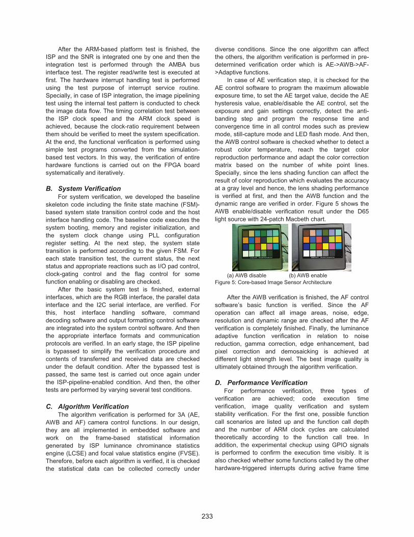
In case of AE verification step, it is checked for the AE control software to program the maximum allowable exposure time, to set the AE target value, decide the AE hysteresis value, enable/disable the AE control, set the exposure and gain settings correctly, detect the anti-banding step and program the response time and convergence time in all control modes such as preview mode, still-capture mode and LED flash mode. And then, the AWB control software is checked whether to detect a robust color temperature, reach the target color reproduction performance and adapt the color correction matrix based on the number of white point lines. Specially, since the lens shading function can affect the result of color reproduction which evaluates the accuracy at a gray level and hence, the lens shading performance is verified at first, and then the AWB function and the dynamic range are verified in order. Figure 5 shows the AWB enable/disable verification result under the D65 light source with 24-patch Macbeth chart.
(a) AWB disable (b) AWB enable
Figure 5: Core-based Image Sensor Architecture
After the AWB verification is finished, the AF control software’s basic function is verified. Since the AF operation can affect all image areas, noise, edge, resolution and dynamic range are checked after the AF verification is completely finished. Finally, the luminance adaptive function verification in relation to noise reduction, gamma correction, edge enhancement, bad pixel correction and demosaicking is achieved at different light strength level. The best image quality is ultimately obtained through the algorithm verification.
D. Performance Verification
For performance verification, three types of verification are achieved; code execution time verification, image quality verification and system stability verification. For the first one, possible function call scenarios are listed up and the function call depth and the number of ARM clock cycles are calculated theoretically according to the function call tree. In addition, the experimental checkup using GPIO signals is performed to confirm the execution time visibly. It is also checked whether some functions called by the other hardware-triggered interrupts during active frame time
���
can affect the execution time. For the second one, the tuning script file is created for both indoor scene and outdoor. Based on this, photos are listed up and appropriate pictures are taken and then their results are compared with competitive pictures. For the last one, it is verified whether the system critical error occurs under complex matrix conditions. The matrix condition is made by changing the number of host access, interrupt triggering, software function call, register access, memory access and so on. System aging test to monitor the internal count or internal state for a long time is realized to increase the system stability. Some more complicate tests, which are corner case test, multiple frames processing test and timing correlation test, are accomplished as well.
V. METHODOLOGY EVALUATION
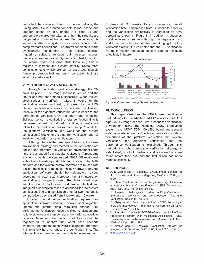
Through the 4-step verification strategy, the 2M pixel/3M pixel ISP of image sensor is verified and the first silicon has been made successfully. When the 2M pixel sensor is verified, it takes 3 weeks for the verification environment setup, 2 weeks for the ARM platform verification, 2 weeks for the system verification, 3weeks for the algorithm verification, and 2 weeks for the performance verification. On the other hand, when the 3M pixel sensor is verified, the total verification time is decreased almost by half. At this time, 2 weeks are taken for the verification environment setup, 1 week for the platform verification, 0.5 week for the system verification, 2 weeks for the algorithm verification and 1.5 week for the performance verification.
Although there is the pixel size difference, the same environment, strategy and method of the verification are applied and therefore the verification environment setup time is decreased from 3weeks to 2weeks. Almost time is spent to verify the synthesized FPGA DB works well without any board-dependent timing error and the ARM platform and the system control software are reused with a slight modification. Because the ISP hardware and the application software should be adequately revised according to pixel size increase, the ISP integration verification is changed in case of the platform verification, and the relative clock speed test, frame rate test and image size conversion test are amended for the system verification. The total verification time for two methods is comparatively decreased from 4 weeks into 1.5 weeks.
However, the algorithm verification requires new application software addition, conventional algorithm update and internal data resolution change. The performance verification needs the fixed verification time to take pictures and then compare them with competitive pictures. Moreover, the function call tree should be regenerated to analyze the worst case scenario whenever the embedded software is changed. Therefore, it is relatively hard to reduce the verification time. The total verification time for two methods is decreased from
5 weeks into 3.5 weeks. As a consequence, overall verification time is decreased from 12 weeks to 7 weeks and the verification productivity is increased by 42% percent as shown in Figure 6. In addition, it becomes possible to run more tests through the regression test and to find more bugs in shorter time. Judging from this verification result, it is estimated that the ISP verification for much higher resolution sensors can be achieved effectively in future.
Methodology Evaluation
1223223 71.520.512
75%
42%
25%33%
50%
33%
0
2
4
6
8
10
12
14
EnvironmentSetup Time
ARM PlatformVerification
Time
SystemVerification
Time
AlgorithmVerification
Time
PerformanceVerification
Time
TotalVerification
Time
Wee
ks
0%
10%
20%
30%
40%
50%
60%
70%
80%
Pro
duct
ivity
Incr
ease
2M Pixel ISP Verification 3M Pixel ISP Verification Verification Productivity Increase Figure 6: Core-based Image Sensor Architecture VI. CONCLUSION
This paper describes the FPGA-based verification methodology for the ARM-based ISP verification of SoC type CMOS image sensor. We present the verification environment using the complete ASIC prototyping system, the ARM7 TDMI CoreTile board and several external interface boards. The 4-step verification strategy comprised of the platform verification, the system verification, the algorithm verification and the performance verification is explained. Through this method, the robust reusable verification strategy is established, a lot of hardware and software bugs are found before tape out, and the first silicon has been made successfully. REFERENCES 1. A. El Gamal and H. Eltoukhy, “CMOS Image Sensors” in
IEEE Circuits and Devices Magazine, May/June. 2005, pp. 6-20.
2. R. Zhou, “System-on-Chip for Mega-pixel digital Camera processor with Auto Control Functions”, IEEE Conference., AISC, Oct. 2003, vol. 2, pp. 894-897.
3. E. Jimenez, “Challenges in System on Chip Verification”, International Workshop on Microprocessor Test and Verification, Dec. 2006, pp.52-60.
4. C. Pixley, et al., “Functional verification 2003: technology, tools and methodology”, International Conference on ASIC, Oct. 2003, Vol.1, pp.1-5.
5. Y. Lin, et al., “Versatile PC/FPGA-Based Verification/Fast Prototyping Platform With multimedia Applications”, IEEE Transactions on Instrumentation and Measurement, Dec. 2007, Vol.2, pp.1490-1495.
6. Y. Mathys and A. Chatelain, “Verification Strategy for Integration 3G Baseband SoC”, DAC, June 2003, pp. 7-10.
7. http://www.huins.com
���