Embed Size (px)
Citation preview
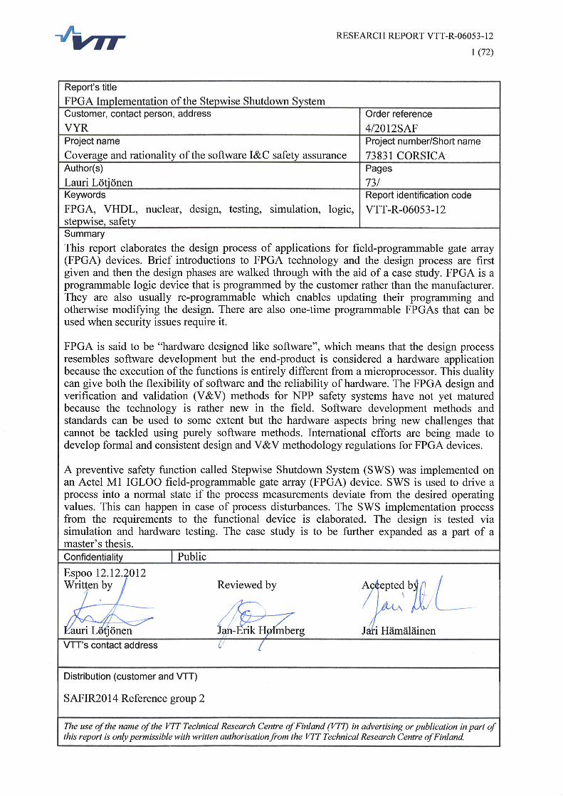
RESEARCH REPORT VTT-R-06053-12
FPGA Implementation of the Stepwise Shutdown System Authors: Lauri Lötjönen
Confidentiality: Public

RESEARCH REPORT VTT-R-06053-12
2 (72)
Contents
List of Acronyms .......................................................................................................... 3
1 Introduction ............................................................................................................. 4
2 Field-Programmable Gate Array ............................................................................. 4
2.1 Hardware ........................................................................................................ 5 2.2 Design ............................................................................................................. 5
2.2.1 Design stages ...................................................................................... 7 2.2.2 Verification & Validation ....................................................................... 8
2.3 VHDL structures .............................................................................................. 9 2.4 Benefits and drawbacks ................................................................................ 11
2.4.1 Benefits .............................................................................................. 11 2.4.2 Drawbacks ......................................................................................... 12
3 Stepwise Shutdown System ................................................................................. 14
3.1 Function ........................................................................................................ 14 3.2 Logic ............................................................................................................. 15
4 Hardware .............................................................................................................. 17
5 Architectural design .............................................................................................. 18
6 Behavioural description ........................................................................................ 19
6.1 Simulation-Only ............................................................................................. 20 6.2 Synthesis ...................................................................................................... 24
7 Simulation ............................................................................................................. 32
7.1 Test bench .................................................................................................... 33 7.2 External files and the simulation interface ..................................................... 40 7.3 Simulation results .......................................................................................... 41
8 Hardware implementation ..................................................................................... 44
9 Conclusions .......................................................................................................... 46
10 References ........................................................................................................... 48
Appendix A: The simulation-only source code ........................................................... 50
Appendix B: The synthesis source code .................................................................... 60
Appendix C: The Tcl source code for the SWSim interface ....................................... 70

RESEARCH REPORT VTT-R-06053-12
3 (72)
List of Acronyms
ASIC Application Specific Integrated Circuit CEC Complex Electronic Component CMOS Complementary Metal Oxide Semiconductor CPU Central Processing Unit EUT Entity-Under-Test FPGA Field-Programmable Gate Array I/O Input/Output IC Integrated Circuit NPP Nuclear Power Plant HDL Hardware Description Language HPD HDL-Programmed Device PAR Place and Route PLD Programmable Logic Device SEE Single Event Effect SRAM Static Random Access Memory SWS Stepwise Shutdown System V&V Verification & Validation VHDL Very High-Speed Integrated Circuit Hardware
Description Language
RESEARCH REPORT VTT-R-06053-12
4 (72)
1 Introduction
Field-programmable gate array (FPGA) is a programmable logic device that can be used to implement very complex logic circuits and perform complex computations. The design process of an FPGA is similar to a software development process but the result is a hardware application. FPGA can thus give both the flexibility of software and the reliability of hardware [1]. FPGA technology is still fairly new in the nuclear industry but the world-wide interest toward the use of FPGA technology in nuclear power plants (NPPs) is rising. The biggest challenge in adopting FPGA more widely in NPPs is the lack of common ground on how the licensing and qualification of FPGA devices should be conducted [1]. This report presents a case study of implementing a preventive safety function called Stepwise Shutdown System (SWS) on an FPGA device. The SWS is used to prevent the process from reaching a state where the actual shutdown needs to be initiated [5]. SWS is actuated if the process state deviates from the desired operating state due to e.g. process disturbances. FPGA technology is first briefly looked into and some hardware and design aspects are elaborated. VHDL, one of the programming languages that are used to make FPGA applications, is then introduced because in the case study, the design source code was written in VHDL. VHDL stands for very high speed integrated circuit hardware description language. Some benefits and drawbacks of using FPGA technology are then considered. An explanation of the functionality of the SWS is given after that, and then the gate-level logic circuit of the SWS is presented. The FPGA device used in the implementation is then described. The following two chapters describe the design process from the source code to the functional device in detail. The simulation and testing methods and results are presented in the last two chapters and then some conclusions are provided. The complete written source code is provided in appendices.
2 Field-Programmable Gate Array
FPGA technology was invented by a company called Xilinx in 1984 [7]. FPGA is a semiconductor device that belongs in the integrated circuit (IC) family. It is classified as a programmable logic device (PLD) and due to its capability to perform very complex computations or logic functions, it is also considered to be a complex electronic component (CEC). The term “field-programmable” refers to the particular characteristic of FPGAs that they are programmed after manufacturing by the customer rather than during manufacture by the manufacturer. Most FPGAs are re-programmable which enables testing different designs and updating existing configurations. FPGA is said to be “hardware designed like software” which means that although FPGAs applications are considered hardware, their design process resembles that of software applications. The
RESEARCH REPORT VTT-R-06053-12
5 (72)
benefit is that FPGAs can provide the flexibility of software and the reliability of hardware [1].
2.1 Hardware
An FPGA usually contains thousands or even millions of system gates, which are memory elements that can be configured in different ways. They are then connected together to form various logic structures. The memory technologies that are used are static random access memory (SRAM), flash and antifuse [1]. This refers to the memory that is used for storing the configuration of the FPGA. The actual system gates are complementary metal oxide semiconductor (CMOS) –based in all three cases. SRAM is the most common technology especially in high-performance applications, since the CMOS manufacturing process is more developed than that of flash technology. However, SRAM memory only holds information while it is powered. If the power is cut, all data is lost. Making a memory element using SRAM technology requires six transistors, which makes the technology more susceptible to faults caused by single event effects (SEEs) such as radiation or other disturbances. Flash technology holds information without power and it only requires one flash transistor to make a memory element. A flash-based device only needs to be programmed once whereas an SRAM-based device needs to be re-programmed every time it is powered up. The antifuse technology is one-time programmable and most resilient to SEEs. The term antifuse comes from a fuse. A fuse is a device designed to cut power when a certain amount of current runs through it. Antifuse works in the opposite way. The programming of an antifuse is “burning” certain signal paths so that a desired configuration is achieved. The design process using different technologies is quite similar but the differences emerge when the operating environment is considered. A high-speed network router might use an SRAM-based FPGA due to high performance requirements and a clean environment, whereas a communication satellite might use an antifuse-based FPGA due to heavy radiation in the orbit. Flash technology could be used in portable devices that require low power consumption and need to be re-programmable. Flash technology is also used in some NPP applications due to start-up times that are faster than using SRAM and the lacking need of an external memory [8]. Flash technology is also more resistant to SEEs due to radiation than SRAM. This makes flash even more susceptible for use in NPPs.
2.2 Design
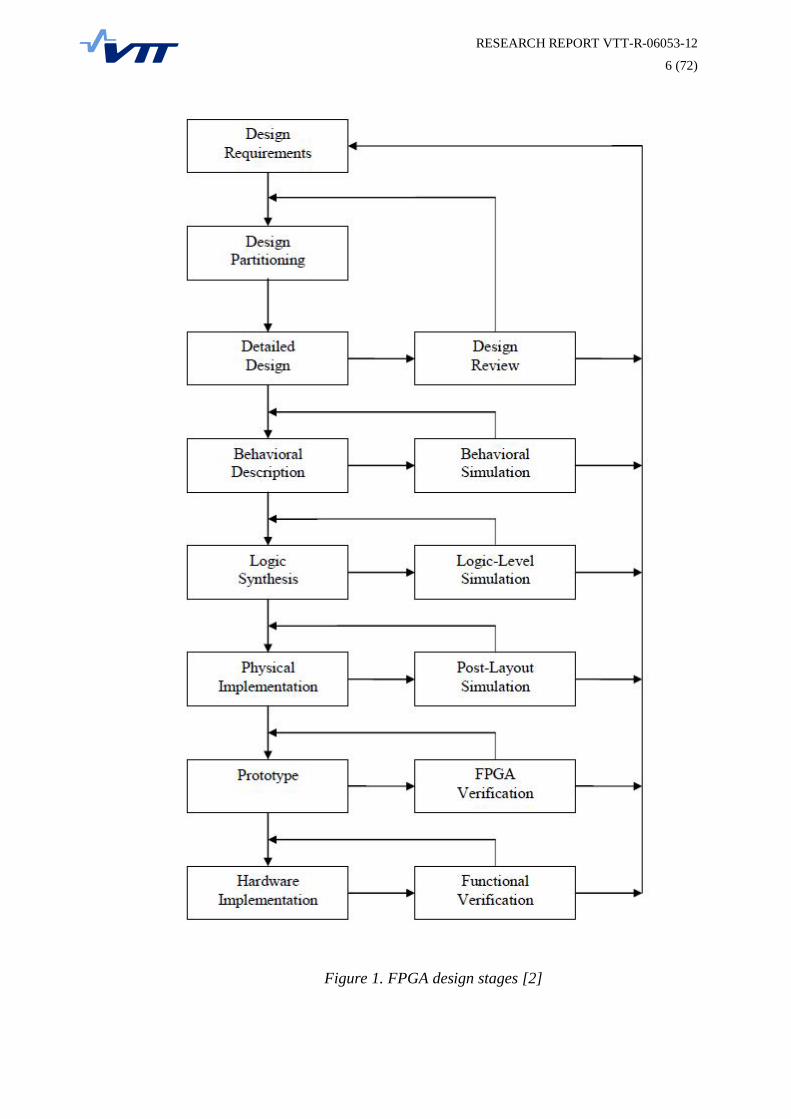
Designing applications for an FPGA device is similar to software design. There is just less abstraction and a few additional steps in process of transforming source code into hardware. In the NRC Review Guidelines [2], there is a comprehensive flowchart of the FPGA design phases that is illustrated in figure 1.
RESEARCH REPORT VTT-R-06053-12
6 (72)
Figure 1. FPGA design stages [2]
RESEARCH REPORT VTT-R-06053-12
7 (72)
2.2.1 Design stages A document containing the Design Requirements is usually a textual description of the desired functionality of the FPGA-based component. The main purpose is to define the functionality but also information about critical timing, power consumption and circuit board size can be included. Design Partitioning is also known as Architectural Design. In it, the functions that implement the requirements are divided into smaller modules and their interactions are defined. All extra features such as redundancy and error-correction are designed in this phase. In Detailed Design, the modules that were designed in Architectural Design are defined in detail. Now issues regarding e.g. memories, clock speed, interfaces and circuitry are considered. This stage results in a description of the design that can be used as an input to the behavioural description. Behavioural description is usually done using a hardware description language (HDL) such as VHDL or Verilog. VHDL is described in more detail in section 2.3. Behaviour can also be described by creating a schematic diagram. It gives the designer more control over design since one automatic compiling stage, synthesis, is skipped. Schematic entry is still recommended for safety-critical applications but is expected to be replaced by the HDL entry method over time because the schematic entry takes a lot more time than HDL entry [2]. The HDL source code can be written using any text editor and then compiled and simulated using simulator software. The behaviour can also be described using languages of higher level of abstraction such as M (Matlab), C or LabVIEW [2]. Automatic code generators are then used to generate HDL code based on the higher level code. This method however involves an extra step of relying on software tools generating code from one language to other. It imposes more requirements on the testing that is already quite rigorous in the case of safety related systems. A low level of detail design usually results in better representation of the original requirements but is much more laborious than higher level design. Depending on the size and criticality of the application, a corresponding level of detail should be chosen for the design method. The next phase is Logic synthesis. In synthesis, the high-level code is transformed into a logic schematic and a netlist that is associated with some internal FPGA resources [6]. The source code is checked in order to verify that it can be synthesised and then the design is optimised with the available resources of the actual device taken into account. The outputs of the synthesis phase are a schematic of the logic and a mid-level netlist which can also be simulated. The next step is called Place and Route (PAR). This phase is also called Physical Implementation in some documents, such as in figure 1, but since the whole case study is about a safety function implementation, the term PAR is used to avoid confusion. In this phase, the synthesised mid-level netlist is converted into a low-level netlist and a bit stream file that can then be used to configure the device. Now the rest of the hardware aspects are considered. The design functionality is achieved through designing the configurations and connections the logic elements
RESEARCH REPORT VTT-R-06053-12
8 (72)
and wirings of the FPGA accordingly. As a result, a detailed model of the physical layout of the configuration is developed. Additionally, a bit stream configuration file is generated. The file is used to configure the actual FPGA device. The results of the PAR can be simulated. After PAR, the design is transferred to the FPGA device. This is called configuration or programming, and it results in a prototype of the design in the device. In programming, the logic elements and wirings of the FPGA are configured and connected with the bit stream configuration file to obtain desired functionality. Hardware implementation means designing the interfaces and the final circuit board fabrication according to the application that the FPGA is going to be used for. The final product can have one or more FPGAs connected to circuit boards that are usually contained in a cabinet to which the IO-signals from a process are connected [1].
2.2.2 Verification & Validation Most of the design stages in figure 1 contain corresponding verification and validation (V&V) activities. The output of the detailed design phase is a textual or graphical representation of the designed partitioning of the logic. The Design Review is reviewing the designed partitioning to make sure it corresponds to the requirements. Also the requirements themselves can be reviewed at this stage. Review can at first be done by the designer but ultimately it should be done by someone who is not involved in the design process. In Behavioral Simulation, the design is tested against the initial system requirements to verify correct behaviour. If the design is modular, the modules can be tested separately in addition to the complete system testing. Usually only small components can be 100% tested but even a component of a few dozen flip-flops has so many states that the 100% testing becomes almost impossible. In the testing, also the unexpected input combinations should be considered because they might be realised for example in the case of malfunctions. The simulation that is done after logic synthesis is called Logic-Level Simulation. Now the hardware aspects are included to some extent. Also, because another automated design generation has been made, this simulation is conducted to make sure that the design still corresponds to the initial requirements. This step should therefore confirm that the outputs are the same as in behavioural simulation when using the same inputs. In Post-Layout Simulation, the hardware aspects can be tested. The exact timing and propagation delay information is now available since the output of PAR is a detailed model of the physical implementation of the design. As before, the outputs should be exactly the same as in the previous simulations to ensure that the design automation tools have not altered the design functionality. In FPGA Verification, the programmed FPGA is tested using hardware generated inputs that are the same as in previous simulation phases. If the PAR and the programming were successful, the outputs should be the same as in the post-layout simulation.
RESEARCH REPORT VTT-R-06053-12
9 (72)
The last V&V phase is Functional Hardware Verification. In it, the FPGA is tested in the actual operating environment. The inputs should cover the expected and the unexpected combinations to make sure that there are no unexpected responses. In this stage, also the external effects such as disturbance caused by nearby electronic components and power surges, which might occur during normal operation, are considered.
2.3 VHDL structures
Very high-speed integrated circuit hardware description language (VHDL) is with Verilog one of the two most used hardware description languages (HDLs) in FPGA design. The language is specified in the IEEE standard 1076 [10]. VHDL can be used to model the behaviour and structure digital systems, and the model can then be simulated or transferred into an FPGA device. However, when making applications for actual devices, only a subset of the language can be used. This subset, called synthesisable VHDL, is described in the IEEE standard 1076.6 [11], which is an expansion to the basic IEEE 1076. The reason for only a subset of VHDL being synthesisable is simply the lack of hardware that could straight away implement many of the complex language constructs such as loops [9]. VHDL resembles Ada which is a language that has been used for many safety- and mission critical applications especially in the USA. It is therefore natural to use VHDL when implementing these kinds of systems in an FPGA, since VHDL is based on a language that has already been used in this environment. Ada has also a good support for concurrent programming and so does VHDL; this makes designing applications for the naturally concurrent FPGA devices easy. Since VHDL is used to model digital systems, a natural way to approach modelling is building the systems from smaller subsystems and basic building blocks such as combinational logic gates. The basic building block in VHDL is an entity. Entities are functional blocks that have an input/output (I/O) -interface and an internal structure. An entity is similar to a class-type in most object-oriented languages. When making applications for synthesis, entities are the actual blocks that are created using the system gates of the FPGA. Inside an entity, there are one or more architectures. The actual functionality of an entity resides in the architectures. There are three types of architectures: behavioural, structural, and mixed behavioural and structural architectures. Behavioural architectures contain processes that contain sequential statements that are executed line by line. Structural architectures do not contain any sequential statements that would define the functionality of the block. Instead, instances of smaller entities are made and connected together to form a functional entity. The behaviour then becomes implicitly defined through the behavioural architectures of the instantiated entities. Mixed architecture contains both sequential and concurrent statements. Below are examples of the basic constructs that were discussed above. entity EXAMPLE is
RESEARCH REPORT VTT-R-06053-12
10 (72)
port( INPUT : in bit ; OUTPUT : out bit ); end entity; Above is an entity declaration. There the I/O-interface is defined by writing the names and types of the ports inside a port declaration. This particular entity has one bit-typed input port INPUT and one bit-typed output port OUTPUT. architecture BEHAVIOURAL of EXAMPLE is begin process ( INPUT ) is OUTPUT <= INPUT; end process; end architecture; The entity EXAMPLE has an architecture called BEHAVIOURAL that contains a process. Inside the process there is only one line of code to be executed and it puts the value of the input to the output port. After the word process, the INPUT is in brackets. This is called a sensitivity list which means that the process is initiated every time any of the signals in the sensitivity list changes value. In this case, every time input changes value, its value is set to the output. architecture STRUCTURAL of EXAMPLE is signal CONNECTOR : bit; begin BLOCK1 : entity work.BLOCK( BEHAVIOUR ) port map( BLOCK_INPUT => INPUT, BLOCK_OUTPUT => CONNECTOR ); BLOCK2 : entity work.BLOCK( BEHAVIOUR ) port map( BLOCK_INPUT => CONNECTOR, BLOCK_OUTPUT => OUTPUT ); end architecture; The architecture above is a structural architecture. There are no processes but instead two instantiations of an entity called BLOCK. The two blocks are connected together by a signal that is defined in the beginning of the architecture. The structure that is defined in the architecture goes as follows: The input port INPUT of the entity EXAMPLE is connected to the input port
BLOCK_INPUT of BLOCK1. To the output of BLOCK1 is connected the signal CONNECTOR.
CONNECTOR is then connected to the input port of BLOCK2. The output of the entity EXAMPLE gets its value from the output port
BLOCK_OUTPUT of BLOCK2. The structural architecture is illustrated in figure 2.

RESEARCH REPORT VTT-R-06053-12
11 (72)
Figure 2. Graphical example of a structural architecture
Now the behaviour of the entity EXAMPLE becomes defined through the behavioural architectures of BLOCK1 and BLOCK2 and their interaction through the signal CONNECTOR. The advantage is that one can build large and complex systems using only basic building blocks that have already been written before.
2.4 Benefits and drawbacks
This section covers some of the benefits and drawbacks of using FPGA technology. The FPGA is compared to application specific integrated circuits (ASICs) and microcontrollers. ASICs and microprocessors can be seen as the main rivals for FPGA technology.
2.4.1 Benefits The first benefit is in performance when compared to a digital signal processor [7]. The parallel nature of an FPGA and the fact that the I/O-ports are controlled at the hardware level provide more processing power in some applications and more accurate matching of application requirements than a digital signal processor. Secondly, the time-to-market can be shorter when using an FPGA versus an ASIC. This is because the designer can test new ideas and concepts on actual hardware by him- or herself, whereas ASICs have to be always fabricated to specification in order to test the design on hardware. Making changes to an FPGA takes hours whereas making new ASICs takes weeks. The third benefit is the cost versus an ASIC. Large quantities of ASICs are not that expensive if no changes are needed to make in them. Many times the devices need to be changed because of, for example changed system requirements or a need for custom functionality. With FPGAs this is a matter of simply modifying the firmware but for ASICs, they have to be re-ordered from the manufacturing plant which takes time and costs a lot of money. The fourth benefit is increased reliability versus microprocessor systems. Microprocessor cores execute one instruction at a time. When running multiple programs in parallel, some execution issues may be encountered due to poor timing of the execution of different threads. An operating system is needed to manage the execution of programs. FPGAs run without an operating system and they run truly concurrent due to the structure of the chip. It is argued that splitting the design into small modules increases reliability [1]. Since it is easy to make modular designs for the naturally modular FPGA, it can be argued that the same functionality made this way is more reliable than a purely

RESEARCH REPORT VTT-R-06053-12
12 (72)
C-language based implementation of the same function because C cannot be used to make modular designs. When using a microprocessor, the instructions are fetched one by one from an external memory and then executed. An FPGA does not execute any instructions but rather runs according to a static configuration that has been done before the start-up. This characteristic of the FPGA is a good example of it not being software but a hardware application. The fifth benefit is regarding long-term maintenance versus ASICs. Many times during the life-cycle of an application, the requirements may change due to, for example, modernization of the plant or simply a need to make an update to the configuration of the device. ASICs always need to be changed because they cannot be modified, whereas re-programmable FPGAs are susceptible to change. One can make the modifications and simulate the new firmware on a PC and then simply transfer the new program to the FPGA, for example, when the plant is in shutdown. When using an FPGA to implement a safety function, it is also easier to demonstrate the independence of the safety functions and the necessary support functions such as management of the I/O communication channels, and self-diagnostic functions [14]. When using a microprocessor, these functions are executed using the same central processing unit (CPU) but when using an FPGA the resources are not shared and the safety functions can be implemented on physically separate devices from the support functions. The prevention of malicious modifications is easier when using FPGAs than microprocessors. The re-programming of the FPGA can be prevented by using antifuse-based FPGAs or flash-based FPGAs that can be locked [1].
2.4.2 Drawbacks The biggest drawback of using an FPGA-based system rather than a microcontroller-based system in NPPs is the lack of commonly accepted design and V&V methods. This is due to the novelty of the technology in NPPs. In some cases, it is not even clear to the regulators what constitutes an FPGA [14]. Although the design process resembles the software design process, a standard for using software in NPPs, such as IEC 60880 [15], cannot be used. However, an IEC standard 62566 [16] is a new standard that has been developed to guide the development and use of HDL-Programmed Devices (HPDs) in NPPs. In many parts of the standard, a corresponding part of the IEC 60880 is instructed to be used with only replacing the word “software” with “HPD”. Compared to software development, in FPGA development the hardware aspects need to be considered. The designer must know the difference between synthesisable and non-synthesisable code. Different devices can also impose different constraints that need to be taken into account. All of the I/O-channels need to be defined and connected to the right pins by the designer. The FPGA design process involves many steps that are different from each other and thus require different software tools. The designer needs to be familiar with

RESEARCH REPORT VTT-R-06053-12
13 (72)
each of these tools and design phases. Software development is quite straightforward: write code, compile the code, product ready. In FPGA development, the first compiling (synthesis) is followed by another compiling (PAR) and then the programming of the device. In software development, the compiling usually consists of more than one step, such as assembling, but this is all done automatically by the compiler and the assembler. In FPGA development, the designer has to make sure that all steps are completed correctly by verifying the design after each step.
RESEARCH REPORT VTT-R-06053-12
14 (72)
3 Stepwise Shutdown System
A logic circuit called Stepwise Shutdown System (SWS) was implemented in an FPGA device. The SWS is a preventive safety-related function, which is used to drive the process into a normal operating state when the process measurements deviate from their desired operating values due to e.g. process disturbances. The implemented function is a simplified version of the actual function. The process measurements that are the inputs to the SWS are handled as one binary signal: if any of the measurements crosses an alarm level, the binary signal is enabled. The logic did not need to be simplified because the process measurements are already handled as a single binary signal. In this example, two versions of the SWS logic were implemented: one that contains a bug which causes the SWS to malfunction in certain situations, and another one that functions correctly. The bugged version was implemented to see if the error in the logic design would be revealed in the FPGA implementation. From now on, these will be referred to as bugged and bug-free versions, respectively. The functionality of the SWS is described in section 3.1 and the logic structures of both versions are illustrated and explained in section 3.2.
3.1 Function When process disturbances cause the process state to deviate from desired operating point, the SWS is used to drive the process back into the normal state. The main purpose of the system is to prevent the process from going into a state where the actual shutdown needs to be initiated. SWS is a preventive safety function. In NPPs, unnecessary process shutdowns are avoided due to safety and economic reasons. If the process deviation is small or the deviation is progressing slowly, SWS will drive the process into a normal operating state without having to rapidly shut the process down. The SWS is diverse from the actual shutdown system but they use partly the same process measurement data. The limit values for the SWS are lower than those for the actual shutdown system. There are four inputs in the system: the first three originate from the process measurements and the last one is the manual input from the operating room. The SWS is triggered if certain conditions in the three measurements from reactor temperature, pressure and in-water flow are met [5]. The manual trip also acts as a criterion for the initiation of the SWS.
Since all of the conditions initiate the SWS functionality in the same way, they are combined as one signal in the implementation. The logic is considered to have only two inputs that are named and from now on will be referred to as process trip and manual trip. Since the logic uses binary signals, the process trip is simply enabled when the process measurements reach certain limit values. The manual trip is a button in the operating room and the signal is enabled when the button is pressed. When either of the inputs initiates the SWS, the process is driven towards a safer state for three seconds. After that, 12 seconds are waited and then the inputs are checked again; if at least one of them is still enabled, the cycle starts again. This is the basic fifteen-second control cycle of the system.
RESEARCH REPORT VTT-R-06053-12
15 (72)
The cycle is continued until a desired operating state is reached or until the higher limits of the process measurements are crossed and the actual shutdown is initiated. By pressing the manual trip from the control room, the operator can initialize a new three-second control during the 12-second idle time. The main difference between the bugged and the bug-free versions of the logic is the way they handle the manual trip. In the bugged version, the manual trip adds a new 3-second pulse but also resets the fifteen-second cycle. In the bug-free version, an additional three-second pulse is added into the cycle without resetting the fifteen-second cycle. The malfunction occurs in the bugged version when the manual trip is pressed while a three-second control is active. The three-second pulse goes on as intended but after that, the output of the system freezes at 0. The reason for this is explained in the next section where the logic structures are elaborated.
3.2 Logic
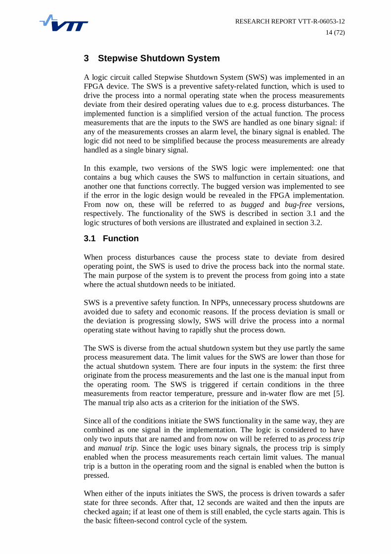
Two simplified versions of the SWS were implemented. For both of them, original logic circuit pictures were provided. The original gate-level structure of the bugged version is in figure 3 and the bug-free version in figure 4. The process trip input, in both designs, is the signal named Input in figures 3 and 4. Originally, all the three signals from the process were separate but since they all go to the OR-gate, where the Input goes, they could as well be combined into a single binary signal that would be enabled if any of the process signals were enabled. Although the manual trip goes to the OR-gate as well, it could not be combined with the process trip, since the manual trip also has other functions such as resetting and initiating pulses. The following is a walkthrough of a situation where one or more of the process measurements reaches the limit value set for the SWS, thus initiating the functionality. The case where the failure of the bugged version occurs is also described.
3s
15s
1 out of 2
Manual trip from control
roomInput 141
Input 241
1 &
1
1
R1
Design AInput
Output
Figure 3. Logic structure of the bugged version
In the bugged version in figure 3, Input (process trip) is enabled, which causes the output of the OR-gate become 1. The enabled output signal of the OR-gate acts as an input to the AND-gate, whose output also becomes 1, since its second input, the inverted output of the fifteen-second pulse gate, is 1. This is because at this point the system output is still 0 and the system output is fed back as the input for the fifteen-second pulse gate whose output is thus 0 as well.
RESEARCH REPORT VTT-R-06053-12
16 (72)
After the AND-gate, there is a three-second pulse gate, which is enabled by a rising edge in the signal. After the AND-gate has thus enabled the three-second pulse gate, the system output is enabled. At the same time, the enabled signal is conveyed to the fifteen-second pulse gate, whose output now turns to 1. This is then inverted and fed to the AND-gate. Now the output of the AND-gate turns to 0 due to the changed value of its second input. Now the input of the three-second pulse is 0 but the pulse goes on until three seconds are up. After that, if the manual trip remains 0, the system output goes to 0 and stays that way for additional twelve seconds due to the fifteen-second pulse still having twelve seconds left in it. After the twelve-second delay, if the process trip is still enabled, the whole cycle begins again. The failure occurs when running the bugged version if the manual trip is pressed during a three-second control. It causes the fifteen-second pulse to reset, which means that the timer is set back to fifteen seconds and the output is made 0. This is then inverted and acts as an input to the AND-gate whose output now goes to 1. When the three-second pulse ends, the input of the fifteen-second pulse gate goes to 0. Since the output of the AND-gate is now 1, the input of the three-second pulse remains at 1. However, since the pulse gate is only activated when there is a rising edge in the input signal, the three-second pulse will not get a rising edge, and the output of the system will thus freeze at 0 until one of the inputs of the AND-gate goes to 0 and back to 1. If the process measurements remain outside the desired levels, the Input would stay at 1, which would cause the system output to remain at 0. Eventually this would either lead to the initiation of the actual shutdown, or the process might recover from the disturbance by itself, thus disabling the process trip and restoring normal operating state.
Figure 4. Logic structure of the bug-free version
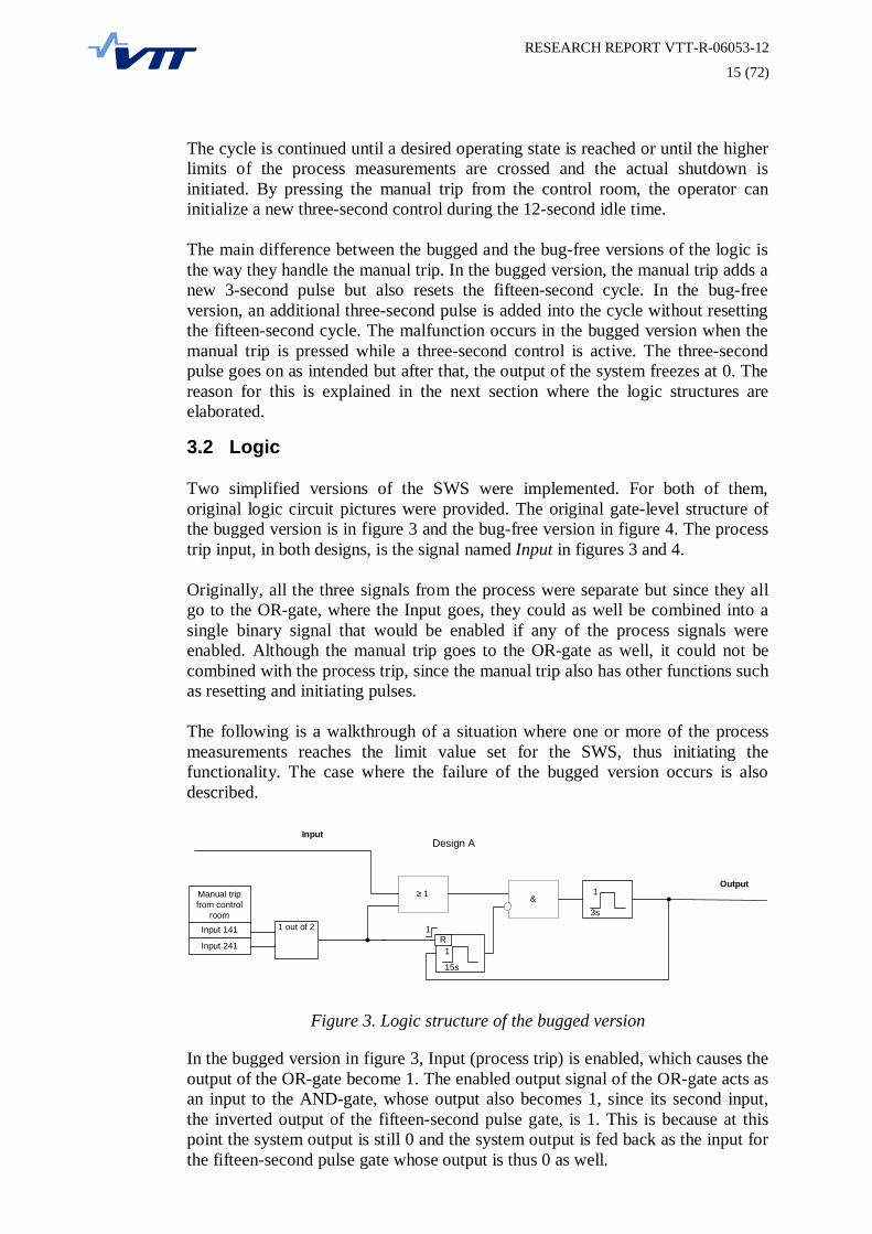
The bug-free version in figure 4 is somewhat different from the bugged version. The main difference is the way that the manual trip is handled. In the bug-free version, the manual trip acts as an input to the OR-gate, and also to an additional OR-gate near the output of the system. There are no resettable pulse gates in the bug-free design and the manual trip is now used to directly affect the output of the system.

RESEARCH REPORT VTT-R-06053-12
17 (72)
The process input stays again at 1 the whole time. If the manual trip is not pressed, the output of the bug-free version is the same as the output of the bugged version. First, the three-second pulse is initiated and then twelve seconds are waited. Since we assumed that Input stays at 1, the cycle then starts again. Now, if the manual trip is pressed, it simply adds an additional three-second pulse via the additional OR-gate near the output of the system. The basic fifteen-second-cycle logic is not affected by it in any way. So now, if the manual trip is pressed during a three-second control pulse, the pulse is simply extended by three seconds. For example, if the control has been on for two seconds and the manual trip is then pressed, the control would stay on for five seconds, since a parallel pulse starts when the manual trip is pressed. Since the basic fifteen-second cycle runs independent of the manual trip, the bug-free version is more efficient and robust than the bugged one even if there was no bug in the bugged version.
4 Hardware
The design was implemented in an M1AGL1000V2-FGG484 FPGA device, manufactured by Actel. The device is designed for portable low-power applications and it has one million system gates [4]. The FPGA was mounted on a development kit that is shown in figure 5.
Figure 5. The M1AGL1000V2-FGG484 FPGA development kit
RESEARCH REPORT VTT-R-06053-12
18 (72)
The size of the development kit circuit board is about 10 cm x 10 cm and the FPGA device itself is about 1.5 cm x 1.5 cm. The development kit has some built-in I/O-devices such as a 10-switch-bank and a reset switch as inputs, and a built-in 10-LED-bank as an output. These built-in I/O-devices and the FPGA are highlighted in figure 5. It is also possible to connect external devices to the development kit via the many additional I/O-ports but for this design, only the built-in I/O-devices were used. In the SWS logic, the input from the process was assigned to switch one on the 10-switch bank. Switch one is the one that is turned to ON position in figure 5. Due to the button-like nature of the manual trip from the control room, it was assigned to the reset switch that is enabled by simply pressing it. The output of the SWS was assigned to the LED-bank such that when the system output is enabled, all of the 10 LEDs are lit. The board has a reprogrammable flash memory, which is good for an iterative design process such as creating and testing a new design, and when switching between different designs. The programming file can be transferred to the flash memory via a micro-USB cable using programming software. The board is powered by either another micro-USB cable or a wall-mounted power source. The wall-mounted power source was used in the case study.
5 Architectural design
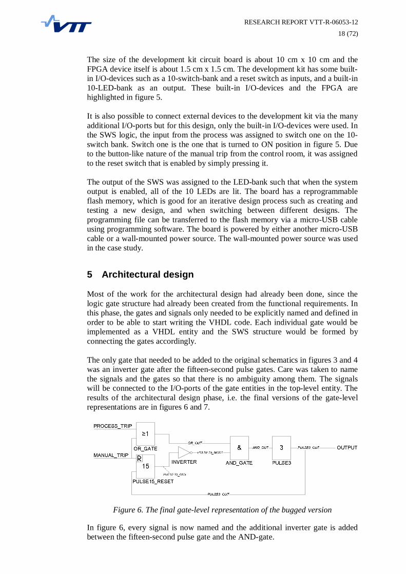
Most of the work for the architectural design had already been done, since the logic gate structure had already been created from the functional requirements. In this phase, the gates and signals only needed to be explicitly named and defined in order to be able to start writing the VHDL code. Each individual gate would be implemented as a VHDL entity and the SWS structure would be formed by connecting the gates accordingly. The only gate that needed to be added to the original schematics in figures 3 and 4 was an inverter gate after the fifteen-second pulse gates. Care was taken to name the signals and the gates so that there is no ambiguity among them. The signals will be connected to the I/O-ports of the gate entities in the top-level entity. The results of the architectural design phase, i.e. the final versions of the gate-level representations are in figures 6 and 7.
Figure 6. The final gate-level representation of the bugged version
In figure 6, every signal is now named and the additional inverter gate is added between the fifteen-second pulse gate and the AND-gate.
RESEARCH REPORT VTT-R-06053-12
19 (72)
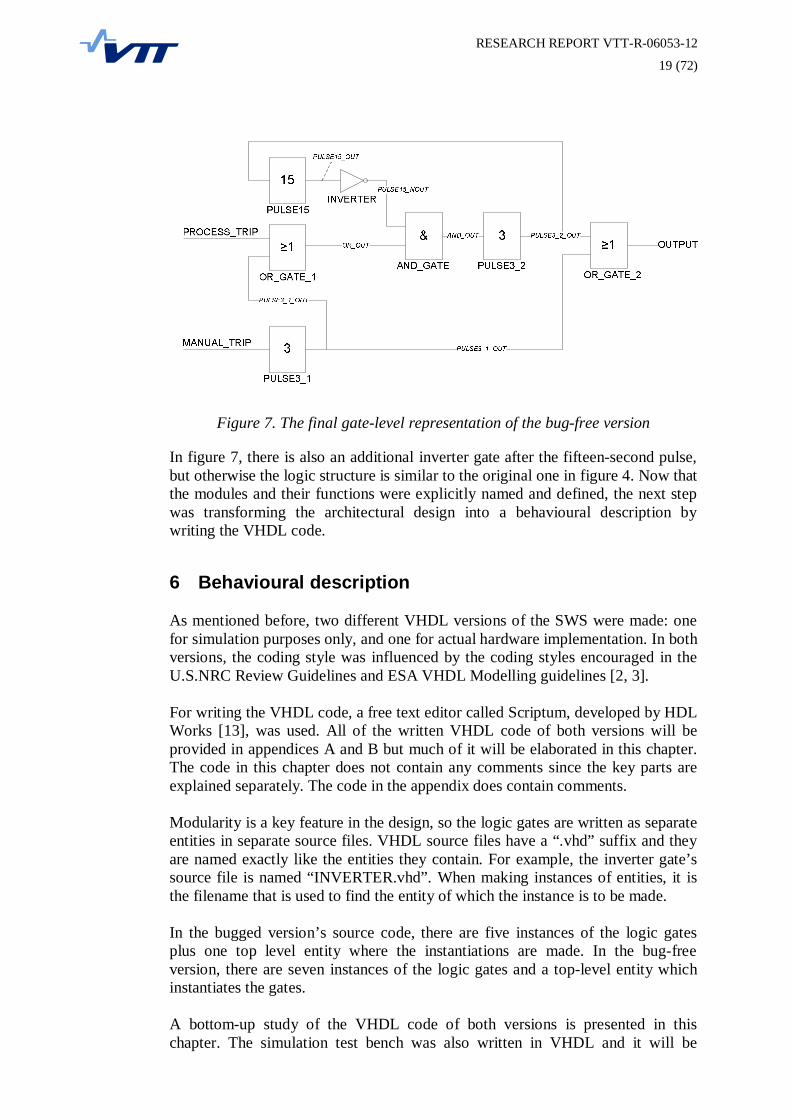
Figure 7. The final gate-level representation of the bug-free version
In figure 7, there is also an additional inverter gate after the fifteen-second pulse, but otherwise the logic structure is similar to the original one in figure 4. Now that the modules and their functions were explicitly named and defined, the next step was transforming the architectural design into a behavioural description by writing the VHDL code.
6 Behavioural description
As mentioned before, two different VHDL versions of the SWS were made: one for simulation purposes only, and one for actual hardware implementation. In both versions, the coding style was influenced by the coding styles encouraged in the U.S.NRC Review Guidelines and ESA VHDL Modelling guidelines [2, 3]. For writing the VHDL code, a free text editor called Scriptum, developed by HDL Works [13], was used. All of the written VHDL code of both versions will be provided in appendices A and B but much of it will be elaborated in this chapter. The code in this chapter does not contain any comments since the key parts are explained separately. The code in the appendix does contain comments. Modularity is a key feature in the design, so the logic gates are written as separate entities in separate source files. VHDL source files have a “.vhd” suffix and they are named exactly like the entities they contain. For example, the inverter gate’s source file is named “INVERTER.vhd”. When making instances of entities, it is the filename that is used to find the entity of which the instance is to be made. In the bugged version’s source code, there are five instances of the logic gates plus one top level entity where the instantiations are made. In the bug-free version, there are seven instances of the logic gates and a top-level entity which instantiates the gates. A bottom-up study of the VHDL code of both versions is presented in this chapter. The simulation test bench was also written in VHDL and it will be
RESEARCH REPORT VTT-R-06053-12
20 (72)
presented in chapter 7. The VHDL code and the language specific keywords will be presented in the following style along with syntax specific colouring: VHDL style example. Section 6.1 concentrates on the VHDL code of the simulation-only version and section 6.2 concentrates on the synthesis version. In section 6.1, a more detailed explanation of the code is given and section 6.2 focuses more on the differences between the two versions.
6.1 Simulation-Only
In order to make a modular design by connecting different gates together inside a top-level entity, the individual gates needed to be created first. Each gate is defined as an individual entity in a separate source file. Since five gates and one top-level entity were needed, six entities were created to implement the simulation-only version of the VHDL code. Their source code will be described in this section. The source code for the AND-gate is presented below. 14 library ieee; 15 use ieee.std_logic_1164.all; 16 17 entity AND2GATE is 18 port ( INPUT1 : in bit ; 19 INPUT2 : in bit ; 20 OUTPUT : out bit ); 21 end entity AND2GATE; 22 23 architecture BEHAVIORAL of AND2GATE is 24 begin 25 26 process ( INPUT1, INPUT2 ) is 27 begin 28 OUTPUT <= INPUT1 and INPUT2; 29 end process; 30 31 end architecture; On lines 14-15, the library ieee and one of its packages std_logic_1164 are employed. The library contains many other packages for different purposes but here only the std_logic_1164 package, which contains logical functions such as and, or, not, etc., is used. The entity declaration on lines 17-21 contains three I/O-port declarations. In the case of this 2-port AND-gate, there are two inputs and one output, all of which are of type bit. The only architecture of the entity is defined on lines 23-30. It contains a process that is sensitive to both inputs, according to the functional description of an AND-gate. In the process, there is only one line of executable code on line 28, which is the assignment of the result of the AND-operation to the output port. The OR-gate is identical to the AND-gate except for the operator inside the process, which is or instead of and. The source code for the OR-gate is presented below. 13 library ieee; 14 use ieee.std_logic_1164.all; 15 16 entity OR2GATE is 17 port ( INPUT1 : in bit ; 18 INPUT2 : in bit ; 19 OUTPUT : out bit ); 20 end entity;
RESEARCH REPORT VTT-R-06053-12
21 (72)
21 22 architecture BEHAVIORAL of OR2GATE is 23 begin 24 process ( INPUT1, INPUT2 ) is 25 begin 26 OUTPUT <= INPUT1 or INPUT2; 27 end process; 28 end architecture; The part where the AND- and OR-gates differ is on line 26 of the OR-gate, where the result of the OR-operation, rather than AND-operation, is assigned to the output. The inverter is quite similar to the previous gates, having one less input port, but just a bit more complex process. The source code for the inverter-gate is presented below. 13 library ieee; 14 use ieee.std_logic_1164.all; 15 16 entity INVERTER is 17 port ( INPUT : in bit ; 18 OUTPUT : out bit ); 19 end entity; 20 21 architecture BEHAVIORAL of INVERTER is 22 begin 23 24 process ( INPUT ) is 25 begin 26 27 if INPUT = '0' then 28 OUTPUT <= '1'; 29 else 30 OUTPUT <= '0'; 31 end if; 32 33 end process; 34 35 end architecture; The architecture of the inverter contains a process where an inverted value of the value on the input port is assigned to the output on lines 27-31. The three basic combinational logic gates were simple and very easy to implement in VHDL because of the ready-made functions such as and and or. The pulse gates were a bit more complex since they include time delays. Fortunately, for simulation purposes, VHDL provides a wait-statement whose variations can be used, for example, to spend an arbitrary amount of time or to wait until a signal is activated. By using the wait-statement, it was very easy to implement both simulation-only version the resettable and the non-resettable pulse gates. The source code for the non-resettable pulse gate is presented below. 13 entity PULSE is 14 generic ( PULSE_LENGTH : time ); 15 port ( INPUT : in bit ; 16 OUTPUT : out bit ); 17 end entity; 18 19 20 21 architecture BEHAVIORAL of PULSE is
RESEARCH REPORT VTT-R-06053-12
22 (72)
22 begin 23 process is 24 begin 25 26 while INPUT'event and INPUT = '1' loop 27 28 OUTPUT <= '1'; 29 wait for PULSE_LENGTH; 30 OUTPUT <= '0'; 31 32 end loop; 33 wait on INPUT; 34 end process; 35 end architecture; The non-resettable pulse gate has an interface of one input and one output and a generic parameter. The generic parameter, defined on line 14, is used to convey the desired pulse length, e.g. three seconds, to the pulse gate when the gate is instantiated in a higher-level entity. This makes the pulse block easily reusable for pulses of different length. As can be seen on line 23, the process-statement does not have a sensitivity list like in the previous gates. This is because, if the wait-statement is used in the process, the sensitivity list cannot reside after the process-statement but instead in the end of the process on line 34. This is just a feature of the VHDL language and does not cause any problems. Because the actual hardware equivalent of the pulse gate includes edge-sensitive flip-flops, the gate was made to be activated when a rising edge is detected on the input signal INPUT. Thus, the first statement after begin initiates a while loop on line 26 with a condition that a rising edge is detected on INPUT. Inside the while-loop, the pulse is initiated on line 28 by assigning a 1 to the output port. After that, the wait for -statement is on line 29 used to initiate a time delay whose length is now specified by the generic parameter PULSE_LENGTH. After the delay, a 0 is assigned to the output on line 30. A pulse of the desired length has now been completed and the gate suspends on line 33 until there is activity on INPUT. The resettable pulse is quite similar to the non-resettable one, having only one additional input RESET, and a somewhat different time delay statement. The parts that are different from the non-resettable pulse gate are presented below. 18 entity PULSE_RESET is 19 generic ( PULSE_LENGTH : time ); 20 port ( INPUT : in bit ; 21 RESET : in bit ; 22 OUTPUT : out bit ); 23 end entity; The additional input RESET is defined on line 21 in addition to the other ports in the entity declaration. 41 wait until RESET'event and RESET = '1' for PULSE_LENGTH; The statement on line 41 corresponds to the wait for –statement on line 29 of the non-resettable pulse gate. In the resettable pulse gate, a rising edge of RESET is waited, but only for a limited time that is specified in the generic parameter PULSE_LENGTH. If no rising edge is detected, the execution is continued after the time delay like in the non-resettable pulse gate. Apart from these parts, the resettable pulse gate is identical to the non-resettable one.
RESEARCH REPORT VTT-R-06053-12
23 (72)
Now that the individual logic gates were completed, it was time to connect them together in a single top-level entity, thus achieving the functionality of SWS. The top-level entity of the simulation-only version of the implementation was named SWS. The entity declaration and the bugged architecture are presented below. 18 library ieee; 19 use ieee.std_logic_1164.all; 20 21 entity SWS is 22 23 port ( PROCESS_TRIP : in bit ; 24 MANUAL_TRIP : in bit ; 25 OUTPUT : out bit ); 26 27 end entity; The top level entity only has two inputs and one output. Additional internal signals are also needed to connect the gates together to form a functional entity. In VHDL, internal signals are created inside an architecture body since they are architecture-specific. The entity declaration is therefore very simple. The entity SWS has two architectures, BUG and BUG_FREE, which correspond to the bugged and the bug-free versions of the logic, respectively. Since the architectures are rather similar to each other and rather long, only the bugged version is presented here. Both versions are included in appendix A. 31 32 architecture BUG of SWS is 33 34 35 signal OR_OUT : bit; 36 signal AND_OUT : bit; 37 signal PULSE15_OUT : bit; 38 signal PULSE15_NOUT : bit; 39 signal PULSE3_OUT : bit; 40 41 42 begin 43 44 45 OUTPUT <= PULSE3_OUT; 46 47 OR_GATE : entity work.OR2GATE(BEHAVIORAL) 48 port map ( INPUT1 => PROCESS_TRIP, 49 INPUT2 => MANUAL_TRIP, 50 OUTPUT => OR_OUT ); 51 52 AND_GATE : entity work.AND2GATE( BEHAVIORAL ) 53 port map ( INPUT1 => OR_OUT, 54 INPUT2 => PULSE15_NOUT, 55 OUTPUT => AND_OUT ); 56 57 INVERTER : entity work.INVERTER( BEHAVIORAL ) 58 port map ( INPUT => PULSE15_OUT, 59 OUTPUT => PULSE15_NOUT ); 60 61 PULSE3 : entity work.PULSE( BEHAVIORAL ) 62 generic map ( PULSE_LENGTH => 3 sec ) 63 port map ( INPUT => AND_OUT,
RESEARCH REPORT VTT-R-06053-12
24 (72)
64 OUTPUT => PULSE3_OUT ); 65 66 PULSE15_RESET : entity work.PULSE_RESET( BEHAVIORAL ) 67 generic map ( PULSE_LENGTH => 15 sec ) 68 port map ( INPUT => PULSE3_OUT, 69 RESET => MANUAL_TRIP, 70 OUTPUT => PULSE15_OUT ); 71 72 end architecture; The internal signals are defined using the signal-statement on lines 35-39. They are named exactly the same way as in figure 6 where the bugged architecture logic was illustrated. The architecture BUG, like the architecture BUG_FREE, is a structural architecture and not a behavioural one. That means that there are no processes and thus no sequential statements that would define the behaviour. The architecture defines a structure whose behaviour of the SWS becomes implicitly defined through the interconnections of the gates that do have behavioural architectures. In the beginning of the architecture on line 45, the output of the three-second pulse gate is assigned to the output port of the top-level entity SWS, since it corresponds to the system output. The separately defined gates are implemented in the entity by creating instances of them. The port map -statement is then used to connect desired internal signals or top-level I/O-ports to the interfaces of the gates. The OR-gate, for example, has been implemented by creating an instance OR_GATE of entity OR2GATE on line 47, and mapping the correct signals to its I/O-ports on lines 48-50. This particular instance of the OR-gate corresponds to the one whose inputs are PROCESS_TRIP and MANUAL_TRIP and whose output is the internal signal OR_OUT. The output is then used as input to the AND-gate, as shown in figure 6. The pulse gates also have generic map –statements, e.g. on lines 62 and 67, which are used to convey the desired length of the pulse.
6.2 Synthesis
This section focuses on the source code of synthesis version of the SWS. The biggest change in the basic combinational gates AND, OR, and the inverter, was making an external clock signal drive the gates. The pulse gates posed a bigger challenge since the wait-statement, which was used in the simulation-only implementation, is not synthesisable and could therefore not be used. Creating a timed pulse became, as initially anticipated, the biggest challenge in implementing the SWS. Where most microcontrollers have a separate timer device for easily creating time delays, an FPGA only has a clock signal, which is generated by an oscillating crystal on the circuit board. Since loops such as while and for are also non-synthesisable, the time delays were created using if-statements and counter variables. All of the synthesis VHDL source files are included in appendix B. The synthesisable source code for the AND-gate is presented below. 14 library ieee; 15 use ieee.std_logic_1164.all; 16 17 entity AND2GATE is 18 port ( CLK : in bit ; 19 INPUT1 : in bit ; 20 INPUT2 : in bit ; 21 OUTPUT : out bit );
RESEARCH REPORT VTT-R-06053-12
25 (72)
22 end entity AND2GATE; 23 24 25 architecture BEHAVIORAL of AND2GATE is 26 27 signal RESULT : bit; 28 29 begin 30 process ( CLK, INPUT1, INPUT2 ) is 31 begin 32 33 if CLK'event and CLK = '1' then 34 RESULT <= INPUT1 and INPUT2; 35 end if; 36 end process; 37 38 39 OUTPUT <= RESULT; 40 41 end architecture; On line 18, the synthesisable AND-gate has an additional input called CLK, which is the clock signal and is conveyed from the top-level entity. On line 27, there is an internal signal called RESULT, which is used to temporarily store the result of the AND-operation during the process. After the process, the value of the signal RESULT is assigned to the output on line 39. The assignment is done outside the process, i.e. concurrently, because the value of the output may be updated at any time instead of as a part of a sequential process. Although the output value assignment is asynchronous, the gate functionality is synchronous, since RESULT is only updated on the rising edge of the clock signal. Apart from the addition of the port CLK and the signal RESULT, the source code is similar to the simulation-only version. The same goes for the other basic combinational gates OR, and the inverter: a clock is added to drive the gate and an internal signal is used for storing the result and assigning it to the output port. The source code for the OR-gate is presented below. 14 library ieee; 15 use ieee.std_logic_1164.all; 16 17 entity OR2GATE is 18 port ( CLK : in bit ; 19 INPUT1 : in bit ; 20 INPUT2 : in bit ; 21 OUTPUT : out bit ); 22 23 end entity; 24 25 architecture BEHAVIORAL of OR2GATE is 26 signal RESULT : bit; 27 begin 28 process ( CLK, INPUT1, INPUT2 ) is 29 begin 30 31 if CLK'event and CLK = '1' then 32 RESULT <= INPUT1 or INPUT2; 33 end if; 34 35 end process; 36
RESEARCH REPORT VTT-R-06053-12
26 (72)
37 OUTPUT <= RESULT; 38 39 end architecture; The clock is the additional input on line 18 and the result is similarly first stored in the RESULT signal and then assigned to the output port outside of the process. The source code of the inverter is below. 14 library ieee; 15 use ieee.std_logic_1164.all; 16 17 entity INVERTER is 18 port ( CLK : in bit ; 19 INPUT : in bit ; 20 OUTPUT : out bit ); 21 end entity; 22 23 24 architecture BEHAVIORAL of INVERTER is 25 signal RESULT : bit; 26 begin 27 process ( CLK, INPUT ) is 28 begin 29 30 if CLK'event and CLK = '1' then 31 if INPUT = '0' then 32 RESULT <= '1'; 33 else 34 RESULT <= '0'; 35 end if; 36 end if; 37 end process; 38 39 40 OUTPUT <= RESULT; 41 42 end architecture; The functionality of the simulation-only pulse gates relied heavily upon the wait-statement. Being non-synthesisable, the wait-statement could not be used in the synthesis version so other methods were needed to generate the time delays. The source code for the non-resettable pulse gate is piecewise presented and elaborated below. 15 entity PULSE is 16 17 generic ( PULSE_LENGTH : integer ; 18 TIME_UNIT : integer ); 19 20 port ( CLK : in bit ; 21 INPUT : in bit ; 22 OUTPUT : out bit ); 23 end entity; Compared to the simulation-only version, the entity PULSE has an additional input CLK and an additional generic parameter TIME_UNIT. In the simulation-only files, the time could be measured and spent in plain seconds, whereas in the synthesis domain, the only thing that has anything to do with time is the clock frequency. The clock was set to 48 MHz, which means that one second can be
RESEARCH REPORT VTT-R-06053-12
27 (72)
spent by doing an operation 48 million times. Thus, the additional generic parameter TIME_UNIT is used to convey the amount of clock cycles that are needed to spend one unit of time. For example, if the time unit is a second, the value of TIME_UNIT would be 48,000,000. A generic parameter was used in order to maintain the possibility of using the gate in situations where the time unit is arbitrary. 27 architecture BEHAVIORAL of PULSE is 28 signal RESULT : bit; 29 begin 30 31 process ( CLK, INPUT ) is 32 variable COUNTER : integer := 0; 33 variable PULSE_ON : bit; 34 variable PREV_INPUT : bit; 35 begin An internal signal RESULT is used, like in the other gates, to store the desired value of the output temporarily during the process. Some variables are also used in the architecture. COUNTER is used to keep record of how many clock cycles have passed. PULSE_ON is a flag that is used to indicate, when the pulse should be on and when it should not be on. PREV_INPUT is used in the end of the process to store the current value of INPUT so that on the next cycle the previous value is known. This is purely a hardware-imposed feature, since the built-in switches on the development kit do not support edge detection. When the previous and the current values of a signal are known, a simple comparison reveals a rising edge, when the signal changes its value. 37 if CLK'event and CLK = '1' then 38 39 40 if INPUT > PREV_INPUT then 41 PULSE_ON := '1'; 42 43 If the current input is larger than the previous one, i.e. the current is 1 and the previous is 0, then there has been a rising edge. The flag PULSE_ON is then turned on to 1. 45 if COUNTER < PULSE_LENGTH*TIME_UNIT then 46 RESULT <= '1'; 47 COUNTER := COUNTER + 1; As long as there is time in the counter, i.e. the pulse length has not been reached, 1 is assigned to RESULT and the counter is incremented. 49 else 50 51 RESULT <= '0'; 52 PULSE_ON := '0'; 53 COUNTER := 0; 54 55 end if;
RESEARCH REPORT VTT-R-06053-12
28 (72)
If the counter has reached the time limit, 0 is assigned to RESULT, flag PULSE_ON is turned to 0 to indicate that the pulse has been given and the counter is reset. 58 elsif COUNTER < PULSE_LENGTH*TIME_UNIT and PULSE_ON = '1' then 59 RESULT <= '1'; 60 COUNTER := COUNTER + 1; 61 else 62 RESULT <= '0'; 63 PULSE_ON := '0'; 64 COUNTER := 0; 65 end if; The elsif-statement on 58 corresponds to the if-statement on line 41. If no rising edge is detected on the input, the pulse is not initiated but may still need to be on due to a previous initiation. This is indicated by the flag PULSE_ON. However, if the pulse has been completed, everything is set to 0. 67 PREV_INPUT := INPUT; 68 69 end if; 70 71 end process; 72 73 OUTPUT <= RESULT; 74 75 end architecture; On line 67, the current input is stored in the end of each clock cycle in order to have the “previous input” during the next cycle. After the process, the value of RESULT is concurrently assigned to the output. As can be seen, it is much more complex to implement a time delay when the aim is to make an application for hardware rather than for simulation. Also, the coding approach has to be different, since the synthesisable code is always just “ran through” during execution. This means that each clock cycle, the whole code is executed and the only way to control it is using the if-statements. When making simulation code, one can use all kinds of loops which make the creation of complex functions easier. The resettable pulse is again quite similar to the non-resettable one. The whole source code is presented below and a yellow background is added to the parts that are functionally different from the non-resettable gate code. 14 library ieee; 15 use ieee.std_logic_1164.all; 16 17 entity PULSE_RESET is 18 19 generic ( PULSE_LENGTH : integer ; 20 TIME_UNIT : integer ); 21 22 23 port ( CLK : in bit ; 24 INPUT : in bit ; 25 RESET : in bit ; 26 OUTPUT : out bit ); 27 end entity; 28 29
RESEARCH REPORT VTT-R-06053-12
29 (72)
30 architecture BEHAVIORAL of PULSE_RESET is 31 signal RESULT : bit; 32 begin 33 34 35 process (CLK, INPUT, RESET ) is 36 37 variable COUNTER : integer := 0; 38 variable PULSE_ON : bit; 39 variable PREV_INPUT : bit; 40 variable PREV_RESET : bit; 41 42 begin 43 44 45 if CLK'event and CLK = '1' then 46 47 48 if INPUT > PREV_INPUT then 49 PULSE_ON := '1'; 50 51 if COUNTER < PULSE_LENGTH*TIME_UNIT and RESET <= PREV_RESET then 52 RESULT <= '1'; 53 COUNTER := COUNTER + 1; 54 else 55 RESULT <= '0'; 56 PULSE_ON := '0'; 57 COUNTER := 0; 58 end if; 59 60 61 62 63 elsif COUNTER < PULSE_LENGTH*TIME_UNIT and PULSE_ON = '1' and RESET <= PREV_RESET then 65 RESULT <= '1'; 66 COUNTER := COUNTER + 1; 67 else 68 RESULT <= '0'; 69 PULSE_ON := '0'; 70 COUNTER := 0; 71 end if; 72 73 PREV_INPUT := INPUT; 74 PREV_RESET := RESET; 75 76 end if; 77 end process; 78 79 80 OUTPUT <= RESULT; 81 82 end architecture; On line 40, a variable PREV_RESET is added to the variable list to store the previous value of the input RESET. This was needed for the rising edge detection. On line 51 is the if-statement which is executed after a rising edge on INPUT has been detected. The RESET now also is checked for a rising edge that would initiate the pulse reset function. On line 63, the elsif-statement is executed when there is no rising edge on INPUT. It also has the additional checking of the
RESEARCH REPORT VTT-R-06053-12
30 (72)
rising edge of RESET. Since the individual gates of the synthesis version were now defined, a top-level entity was to be created. The entity declaration and the bugged architecture are presented below. 18 library ieee; 19 use ieee.std_logic_1164.all; 20 21 entity topLevel is 22 23 port ( CLK : in bit; 24 RST_N : in bit; 25 SWITCHES : in bit_vector(9 downto 0); 26 LEDS : out bit_vector(9 downto 0)); 27 28 end entity; The declaration part of the top-level entity now contains the actual I/O-ports of the FPGA device: CLK is the external clock signal, RST_N is the active low reset switch which is connected to the reset switch in figure 5 and SWITCHES and LEDS are the built-in switch- and LED-banks in figure 5. The switches and leds act as 10-bit binary vector. If for example switch 1 on the switch-bank is turned to ON-position, the bit 0 in the SWITCHES vector turns to 1. Same goes for the LEDs: if bit 0 of signal LEDS is turned to 1, the rightmost LED in the LED-bank lights up on the board. 50 architecture BUG_FREE of topLevel is 51 52 signal AND_OUT : bit; 53 signal OR_OUT : bit; 54 signal PULSE3_1_OUT : bit; 55 signal PULSE3_2_OUT : bit; 56 signal PULSE15_OUT : bit; 57 signal PULSE15_NOUT : bit; 58 signal PROCESS_TRIP : bit; 59 signal MANUAL_TRIP : bit; 60 signal OUTPUT : bit; 61 62 constant SECOND : integer := 48000000; The signal list is similar to the one in the simulation-only version with the addition of the signals PROCESS_TRIP and MANUAL_TRIP. These are used in the I/O-ports of the components and the values of the actual I/O-ports of the FPGA are assigned to them. In this case, the SWS I/O-ports process trip and manual trip were assigned to the specific LEDs and switches but they could be changed without having to re-assign the component I/O-ports thanks to the additional internal signals PROCESS_TRIP and MANUAL_TRIP. The constant SECOND is used to convey the time unit to the pulse gates. It represents the clock cycle amount needed to spend one second. 64 component PULSE is 65 generic( PULSE_LENGTH : integer ; 66 TIME_UNIT : integer ); 67 port( CLK : in bit ; 68 INPUT : in bit ; 69 OUTPUT : out bit ); 70 end component;
RESEARCH REPORT VTT-R-06053-12
31 (72)
This time the gates are instantiated using the component-statement. The way the instantiations were done in the simulation-only version is not synthesisable. After the declaration of the component PULSE, the remaining four gates are declared in a similar fashion. The component declaration acts as a header for the component and thus enables the creation of instances of that particular component in the architecture body. The synthesis tool looks for a file of the same name as the name given after component in the directory where the top-level entity source code is located. It is therefore encouraged to give the source code files the same name as the entities they comprise and store all of the related source files together in the same directory. 71 component AND2GATE is 72 port( CLK : in bit ; 73 INPUT1 : in bit ; 74 INPUT2 : in bit ; 75 OUTPUT : out bit ); 76 end component; 77 78 79 component INVERTER is 80 port( CLK : in bit ; 81 INPUT : in bit ; 82 OUTPUT : out bit ); 83 end component; 84 85 86 component OR2GATE is 87 port( CLK : in bit ; 88 INPUT1 : in bit ; 89 INPUT2 : in bit ; 90 OUTPUT : out bit ); 91 end component; 92 93 begin 94 95 PROCESS_TRIP <= SWITCHES(0); 96 MANUAL_TRIP <= not RST_N; 97 LEDS <= (others => OUTPUT); In the beginning of the architecture body, after the begin-statement on line 95, the values of the input ports SWITCHES(0) and RST_N are assigned to internal signals. The value of PULSE3_OUT, which is the system output in the bugged version, is assigned to the output i.e. the whole LED-bank. Only the first switch is used as an input in the logic, which is why there is the index (0) in SWITCHES(0). Since the physical reset switch RST_N is active low, its inverted value must be used in the logic. The others-statement, when assigning values to the LEDs, simply means that the value of the one-bit signal PULSE3_OUT is assigned to all 10 LEDs in the bank. 106 AND_GATE : component AND2GATE 107 port map ( CLK => CLK, 108 INPUT1 => PULSE15_NOUT, 109 INPUT2 => OR_OUT, 110 OUTPUT => AND_OUT ); 111 112 INV_GATE : component INVERTER 113 port map ( CLK => CLK, 114 INPUT => PULSE15_OUT,
RESEARCH REPORT VTT-R-06053-12
32 (72)
115 OUTPUT => PULSE15_NOUT ); 116 117 OR_GATE_1 : component OR2GATE 118 port map ( CLK => CLK, 119 INPUT1 => PROCESS_TRIP, 120 INPUT2 => PULSE3_1_OUT, 121 OUTPUT => OR_OUT ); 122 123 OR_GATE_2 : component OR2GATE 124 port map ( CLK => CLK, 125 INPUT1 => PULSE3_2_OUT, 126 INPUT2 => PULSE3_1_OUT, 127 OUTPUT => OUTPUT ); 128 129 PULSE3_1 : component PULSE 130 generic map ( PULSE_LENGTH => 3, 131 TIME_UNIT => SECOND ) 132 port map ( CLK => CLK, 133 INPUT => MANUAL_TRIP, 134 OUTPUT => PULSE3_1_OUT ); 135 136 PULSE3_2 : component PULSE 137 generic map ( PULSE_LENGTH => 3, 138 TIME_UNIT => SECOND ) 139 port map ( CLK => CLK, 140 INPUT => AND_OUT , 141 OUTPUT => PULSE3_2_OUT ); 142 143 PULSE15 : component PULSE 144 generic map ( PULSE_LENGTH => 15, 145 TIME_UNIT => SECOND ) 146 port map ( CLK => CLK, 147 INPUT => PULSE3_2_OUT, 148 OUTPUT => PULSE15_OUT ); 149 150 end architecture; The component instantiations are done last. The same generic and port map statements are used as in the simulation-only version. This ends the bugged architecture. In the source file, there is also the error free version but it is not presented here. When both simulation and synthesis versions of the source code were completed, the next step was testing the design through simulation and hardware testing.
7 Simulation
The simulation-only version of the logic was tested through simulation with Mentor Graphics’ ModelSim software [12]. The tests covered the case where the bugged version works correctly and the case where it fails due to the specific manual trip input trajectory. The same inputs were used on the bug-free version simply to show that it does not fail. The synthesis version was not tested by simulation because the clock signal frequency is so high that simulating the design would have taken too long. The problem is that the SWS is run at second-scale and the clock ticks at nanosecond-scale. Therefore, the simulation resolution would have needed to be set to nanosecond.
RESEARCH REPORT VTT-R-06053-12
33 (72)
Seven cases were tested through simulation. In all cases, the SWS was run for thirty seconds. The following cases where tested:
1. “Process trip on” = process trip is enabled after one second of simulation and then kept on indefinitely. This test verifies that the fifteen-second control cycle works correctly.
2. “Process trip on and off” = process enabled after one second of simulation and kept on for one second. This test verifies that there are no extra control cycles when the criteria are disabled.
3. “Manual trip on” = identical to the first test case except that manual trip is now used instead of process trip.
4. “Manual trip on and off” = identical to second test case except that manual trip is now used instead of process trip.
5. “Manual trip in the middle” = process trip is enabled one second after simulation. Manual trip is then enabled for half a second after nine seconds of total simulation. This test verifies the correct functioning of the addition of the extra pulse during the fifteen-second control cycle.
6. “Freeze” = process trip is enabled after one second of simulation. Two seconds later, during the first three-second control, manual trip is enabled for half a second. Manual trip is then pressed again after eight seconds of total simulation. This test reveals the bug in the bugged version and verifies the correct functioning of the bug-free version in the same situation.
7. “Freeze and continue” = The case is similar to the sixth case but process trip is set to 0 after nine and a half seconds of total simulation for one second. The test verifies that even the bugged version returns to normal operation if the criteria are disabled when the system has frozen.
The test bench also prints the simulation results from each stimulus file into respective output-files. The testing can be done completely without the graphical user interface of ModelSim, since a command prompt interface was also created for running the simulator. The test bench, the command prompt interface and finally the simulation results are presented in this chapter.
7.1 Test bench
The test bench was also written in VHDL and it makes use of a VHDL package called textio, which enables reading from and writing to external files. The test bench could be created without any connection to external files but then each test would have to be written into the source code. Then, every time the test cases would need to be changed, the code would have to be re-written and re-compiled, which is time consuming and inefficient. There is commercial software such as Waveformer by Synapticad that can be used to automatically create VHDL stimulus files such software was not used in this study. The test bench that was created can be used for comprehensive testing because the stimulus files are of such generic nature, that creating them does not require any knowledge of e.g. programming or VHDL. The stimulus files will be presented in section 7.2.
RESEARCH REPORT VTT-R-06053-12
34 (72)
The source code of the test bench contains one procedure, a concurrent part and a process, which are now presented in this order. 27 library ieee; 28 use ieee.std_logic_1164.all; 29 use ieee.std_logic_arith.all; 30 use std.textio.all; 31 32 entity TEST_BENCH is 33 generic( STIM_FILENAME : string ; 34 OUTPUT_FILENAME : string ); 35 end entity; Since the test bench uses the textio package, it is enabled on line 30. On lines 32-35 is the entity declaration. Usually test benches are self-contained, i.e. they do not have any kind of an interface. However, since our test bench deals with external files, two generic parameters are now used to convey the names of both the stimulus file and the output file. 37 architecture TEST of TEST_BENCH is 38 39 40 file STIM_FILE : text open read_mode is STIM_FILENAME; 41 file OUTPUT_FILE : text open write_mode is OUTPUT_FILENAME; 42 43 44 constant RESOLUTION : time := ms; 45 constant TIME_UNIT : string := "[ms] "; 46 47 48 signal PROCESS_TRIP : bit; 49 signal MANUAL_TRIP : bit; 50 signal OUTPUT1 : bit; 51 signal OUTPUT2 : bit; 52 signal WRITE_DRIVER : bit; 53 signal FIRST_LINE_WRITTEN : bit;
The test bench has one architecture, and its files, constants and signals are defined on lines 40-53. First, on lines 40-41, two files are created. file is a VHDL type that can be used to manipulate actual external files. When a file is created, a pointer to a file specified by a parameter (now a generic parameter) is actually created. After the files, on lines 44-45, two constants are defined. RESOLUTION specifies the time resolution of the print file. Now, since the resolution is ms, the printing interval of the output file is one millisecond. The other constant is just used in the header part of the output to print the resolution that is used. The signal declarations are on lines 48-53. The first three signals are the ones that are used in the ports of the SWS. Because both versions are simulated at the same time, two output signals are needed. The output of the bugged version is assigned to OUTPUT1 and the output of the bug-free version is assigned to OUTPUT2. WRITE_DRIVER drives the output writing procedure. Its value changes every RESOLUTION and every time it changes value, the writing procedure is called. This is how the RESOLUTION determines the time resolution of the output file.
RESEARCH REPORT VTT-R-06053-12
35 (72)
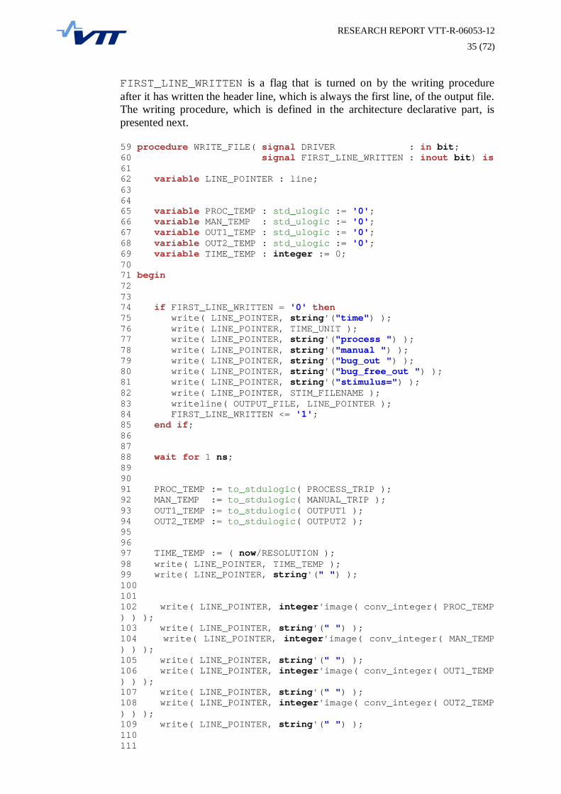
FIRST_LINE_WRITTEN is a flag that is turned on by the writing procedure after it has written the header line, which is always the first line, of the output file. The writing procedure, which is defined in the architecture declarative part, is presented next.
59 procedure WRITE_FILE( signal DRIVER : in bit; 60 signal FIRST_LINE_WRITTEN : inout bit) is 61 62 variable LINE_POINTER : line; 63 64 65 variable PROC_TEMP : std_ulogic := '0'; 66 variable MAN_TEMP : std_ulogic := '0'; 67 variable OUT1_TEMP : std_ulogic := '0'; 68 variable OUT2_TEMP : std_ulogic := '0'; 69 variable TIME_TEMP : integer := 0; 70 71 begin 72 73 74 if FIRST_LINE_WRITTEN = '0' then 75 write( LINE_POINTER, string'("time") ); 76 write( LINE_POINTER, TIME_UNIT ); 77 write( LINE_POINTER, string'("process ") ); 78 write( LINE_POINTER, string'("manual ") ); 79 write( LINE_POINTER, string'("bug_out ") ); 80 write( LINE_POINTER, string'("bug_free_out ") ); 81 write( LINE_POINTER, string'("stimulus=") ); 82 write( LINE_POINTER, STIM_FILENAME ); 83 writeline( OUTPUT_FILE, LINE_POINTER ); 84 FIRST_LINE_WRITTEN <= '1'; 85 end if; 86 87 88 wait for 1 ns; 89 90 91 PROC_TEMP := to_stdulogic( PROCESS_TRIP ); 92 MAN_TEMP := to_stdulogic( MANUAL_TRIP ); 93 OUT1_TEMP := to_stdulogic( OUTPUT1 ); 94 OUT2_TEMP := to_stdulogic( OUTPUT2 ); 95 96 97 TIME_TEMP := ( now/RESOLUTION ); 98 write( LINE_POINTER, TIME_TEMP ); 99 write( LINE_POINTER, string'(" ") ); 100 101 102 write( LINE_POINTER, integer'image( conv_integer( PROC_TEMP ) ) ); 103 write( LINE_POINTER, string'(" ") ); 104 write( LINE_POINTER, integer'image( conv_integer( MAN_TEMP ) ) ); 105 write( LINE_POINTER, string'(" ") ); 106 write( LINE_POINTER, integer'image( conv_integer( OUT1_TEMP ) ) ); 107 write( LINE_POINTER, string'(" ") ); 108 write( LINE_POINTER, integer'image( conv_integer( OUT2_TEMP ) ) ); 109 write( LINE_POINTER, string'(" ") ); 110 111
RESEARCH REPORT VTT-R-06053-12
36 (72)
112 writeline( OUTPUT_FILE, LINE_POINTER ); 113 114 end procedure WRITE_FILE;
On lines 59-60 the procedure is declared. Here the arguments of the procedure are defined. The procedure can read the signal DRIVER, and it can read and write the value of the flag FIRST_LINE_WRITTEN. The driver needs to be an argument because the procedure is called in the concurrent section of the architecture so the argument-list acts as a sensitivity list, like in a process. If there was no driving signal, and the procedure was called from a concurrent section, the simulation would not run because the procedure would be called again and again at time 0 without advancing. The first variable to be defined, on line 62, is a pointer to a line of text. Writing happens so that the line pointer is first filled with text or numbers or other printable data, then the whole line is written into the file using. After the line pointer, the next variables on lines 65-68 are used to temporarily convert the bit-typed signals PROCESS_TRIP, MANUAL_TRIP, OUTPUT1 and OUTPUT2 to std_ulogic-type. OUTPUT1 is the output from the bugged version and OUTPUT2 is the output from the bug-free version. The conversions are done because the write-functions do not accept bit-types, but do accept for example std_ulogic-type. The last variable TIME_TEMP on line 69 is used to convert the current time from a time-type to an integer. This is done to get as generic as possible a format for the timestamps in the output files. In the sequential part of the WRITE_FILE procedure, starting from line 71, the header information is first printed into the file. The flag FIRST_LINE_WRITTEN is set to 0 when the program starts so when the procedure is called for the first time, the expression after the if-statement on line 74 evaluates as true, and the header printing commences. As mentioned before, writing to a file is done so that first a line pointer is filled with data and then the whole line is written into a file. On lines 75-82 one integer and several strings are added to the line pointer and on line 83 the contents of the pointer are written into the specified external file. The writeline-statement also empties the line pointer. On line 84, the flag FIRST_LINE_WRITTEN is then turned to 1 and it stays that way indefinitely. That way the header is only written once. Below is an example of a header from an output file. time[ms] process manual output stimulus=c:/data/stimulus/stim1.txt The printing of the simulation results starts from line 88. There is a wait for-statement, which is required in order for all the processes in the SWS to finish before the results are written into the file. The simulator does not know about the hierarchy of the different processes and entities and therefore does not automatically wait for the processes to finish. Only time delays can help the simulator to determine the executing order of the different parts of the program.
RESEARCH REPORT VTT-R-06053-12
37 (72)
Although the delay on the wait for-statement is 1 nanosecond, it is evaluated as 0, because the resolution of the simulator is one millisecond. The simulator still takes the delay into account by letting all of the processes finish before continuing to the next lines after the wait for-statement. The simulator resolution could be set smaller but then the simulation would take much more time, since the logic is always simulated for several tens of seconds. Also, the time constants of the logic are of a second-scale so therefore a resolution of one millisecond was considered to be sufficiently small. On lines 91-94, the bit-typed signals are converted to a different type in order to be able to use the write-command. On line 97-100, the current time is first converted to an integer by dividing the time-typed now with the time-typed RESOLUTION. The now-variable is automatically created and updated by the simulator so it always contains the correct current simulation time. After that, the current time is written into the line pointer and. The timestamp is written first, because the current time runs in the first column of the output file. Next, on lines 102-109, the values of the input and output signals are written into the line pointer in the correct order. Spaces are printed after each signal to separate them. After that, on line 112, the line that contains the timestamp and the signal values is written into the external output file. An example of such a line is below. 1142 1 0 1 1
The line above would correspond to a situation where the simulation has been running for 1142 milliseconds, the process trip input is 1, the manual trip input is 0, the bugged version output is 1 and the bug-free version output is 1. After the procedure, the architecture body begins. 125 begin 126 127 BUG : entity work.SWS( BUG ) 128 port map ( PROCESS_TRIP => PROCESS_TRIP, 129 MANUAL_TRIP => MANUAL_TRIP, 130 OUTPUT => OUTPUT1 ); 131 132 133 BUG_FREE : entity work.SWS( BUG_FREE ) 134 port map ( PROCESS_TRIP => PROCESS_TRIP, 135 MANUAL_TRIP => MANUAL_TRIP, 136 OUTPUT => OUTPUT2 ); 137 138 139 140 WRITE_DRIVER <= not WRITE_DRIVER after RESOLUTION; 141 WRITE_FILE( WRITE_DRIVER, FIRST_LINE_WRITTEN ); First in the architecture body, instances of both versions of the SWS are created on lines 127-130 and 133-136. After that, on line 140 a driving clock-like signal is generated for calling the WRITE_FILE procedure, which is then called on line 141. Because the DRIVER is flipped every RESOLUTION (time units), the RESOLUTION thus determines the output file printing resolution. The
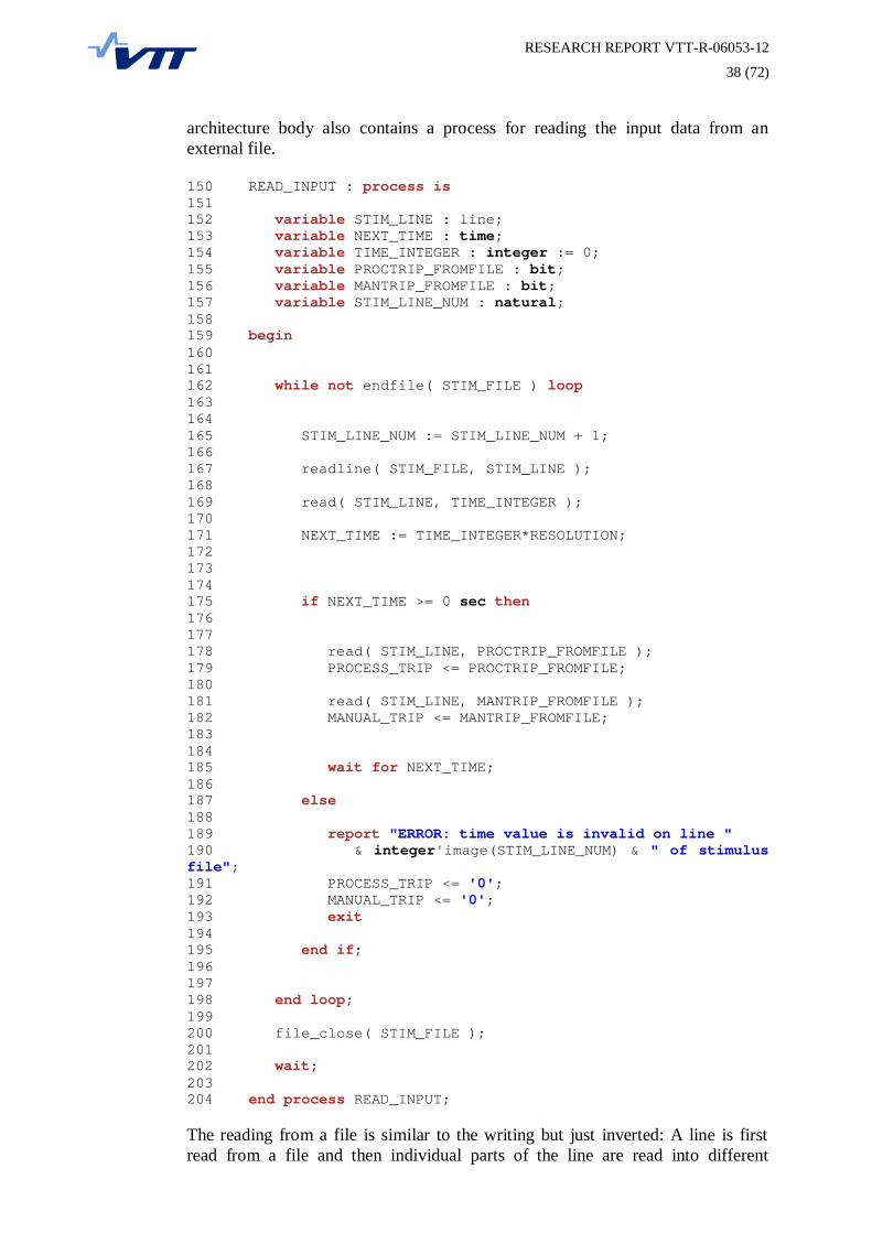
RESEARCH REPORT VTT-R-06053-12
38 (72)
architecture body also contains a process for reading the input data from an external file. 150 READ_INPUT : process is 151 152 variable STIM_LINE : line; 153 variable NEXT_TIME : time; 154 variable TIME_INTEGER : integer := 0; 155 variable PROCTRIP_FROMFILE : bit; 156 variable MANTRIP_FROMFILE : bit; 157 variable STIM_LINE_NUM : natural; 158 159 begin 160 161 162 while not endfile( STIM_FILE ) loop 163 164 165 STIM_LINE_NUM := STIM_LINE_NUM + 1; 166 167 readline( STIM_FILE, STIM_LINE ); 168 169 read( STIM_LINE, TIME_INTEGER ); 170 171 NEXT_TIME := TIME_INTEGER*RESOLUTION; 172 173 174 175 if NEXT_TIME >= 0 sec then 176 177 178 read( STIM_LINE, PROCTRIP_FROMFILE ); 179 PROCESS_TRIP <= PROCTRIP_FROMFILE; 180 181 read( STIM_LINE, MANTRIP_FROMFILE ); 182 MANUAL_TRIP <= MANTRIP_FROMFILE; 183 184 185 wait for NEXT_TIME; 186 187 else 188 189 report "ERROR: time value is invalid on line " 190 & integer'image(STIM_LINE_NUM) & " of stimulus file"; 191 PROCESS_TRIP <= '0'; 192 MANUAL_TRIP <= '0'; 193 exit 194 195 end if; 196 197 198 end loop; 199 200 file_close( STIM_FILE ); 201 202 wait; 203 204 end process READ_INPUT; The reading from a file is similar to the writing but just inverted: A line is first read from a file and then individual parts of the line are read into different
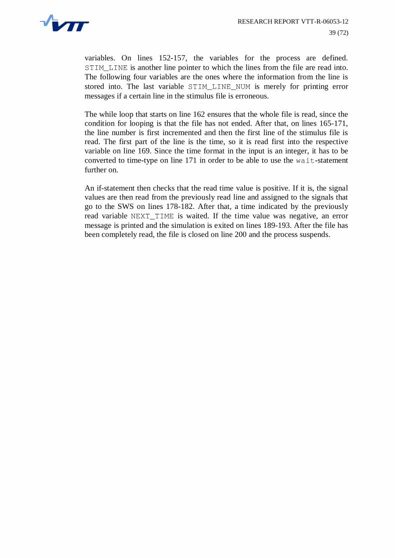
RESEARCH REPORT VTT-R-06053-12
39 (72)
variables. On lines 152-157, the variables for the process are defined. STIM_LINE is another line pointer to which the lines from the file are read into. The following four variables are the ones where the information from the line is stored into. The last variable STIM_LINE_NUM is merely for printing error messages if a certain line in the stimulus file is erroneous. The while loop that starts on line 162 ensures that the whole file is read, since the condition for looping is that the file has not ended. After that, on lines 165-171, the line number is first incremented and then the first line of the stimulus file is read. The first part of the line is the time, so it is read first into the respective variable on line 169. Since the time format in the input is an integer, it has to be converted to time-type on line 171 in order to be able to use the wait-statement further on. An if-statement then checks that the read time value is positive. If it is, the signal values are then read from the previously read line and assigned to the signals that go to the SWS on lines 178-182. After that, a time indicated by the previously read variable NEXT_TIME is waited. If the time value was negative, an error message is printed and the simulation is exited on lines 189-193. After the file has been completely read, the file is closed on line 200 and the process suspends.
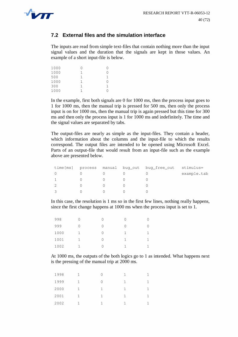
RESEARCH REPORT VTT-R-06053-12
40 (72)
7.2 External files and the simulation interface
The inputs are read from simple text-files that contain nothing more than the input signal values and the duration that the signals are kept in those values. An example of a short input-file is below. 1000 0 0 1000 1 0 500 1 1 1000 1 0 300 1 1 1000 1 0 In the example, first both signals are 0 for 1000 ms, then the process input goes to 1 for 1000 ms, then the manual trip is pressed for 500 ms, then only the process input is on for 1000 ms, then the manual trip is again pressed but this time for 300 ms and then only the process input is 1 for 1000 ms and indefinitely. The time and the signal values are separated by tabs. The output-files are nearly as simple as the input-files. They contain a header, which information about the columns and the input-file to which the results correspond. The output files are intended to be opened using Microsoft Excel. Parts of an output-file that would result from an input-file such as the example above are presented below. time[ms] process manual bug_out bug_free_out stimulus=
0 0 0 0 0 example.tab
1 0 0 0 0
2 0 0 0 0
3 0 0 0 0
In this case, the resolution is 1 ms so in the first few lines, nothing really happens, since the first change happens at 1000 ms when the process input is set to 1. 998 0 0 0 0
999 0 0 0 0
1000 1 0 1 1
1001 1 0 1 1
1002 1 0 1 1 At 1000 ms, the outputs of the both logics go to 1 as intended. What happens next is the pressing of the manual trip at 2000 ms. 1998 1 0 1 1
1999 1 0 1 1
2000 1 1 1 1
2001 1 1 1 1
2002 1 1 1 1
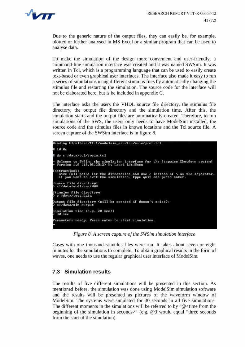
RESEARCH REPORT VTT-R-06053-12
41 (72)
Due to the generic nature of the output files, they can easily be, for example, plotted or further analysed in MS Excel or a similar program that can be used to analyse data. To make the simulation of the design more convenient and user-friendly, a command-line simulation interface was created and it was named SWSim. It was written in Tcl, which is a programming language that can be used to easily create text-based or even graphical user interfaces. The interface also made it easy to run a series of simulations using different stimulus files by automatically changing the stimulus file and restarting the simulation. The source code for the interface will not be elaborated here, but is be included in appendix C. The interface asks the users the VHDL source file directory, the stimulus file directory, the output file directory and the simulation time. After this, the simulation starts and the output files are automatically created. Therefore, to run simulations of the SWS, the users only needs to have ModelSim installed, the source code and the stimulus files in known locations and the Tcl source file. A screen capture of the SWSim interface is in figure 8.
Figure 8. A screen capture of the SWSim simulation interface
Cases with one thousand stimulus files were run. It takes about seven or eight minutes for the simulations to complete. To obtain graphical results in the form of waves, one needs to use the regular graphical user interface of ModelSim.
7.3 Simulation results
The results of five different simulations will be presented in this section. As mentioned before, the simulation was done using ModelSim simulation software and the results will be presented as pictures of the waveform window of ModelSim. The systems were simulated for 30 seconds in all five simulations. The different moments in the simulations will be referred to by “@<time from the beginning of the simulation in seconds>” (e.g. @3 would equal “three seconds from the start of the simulation).
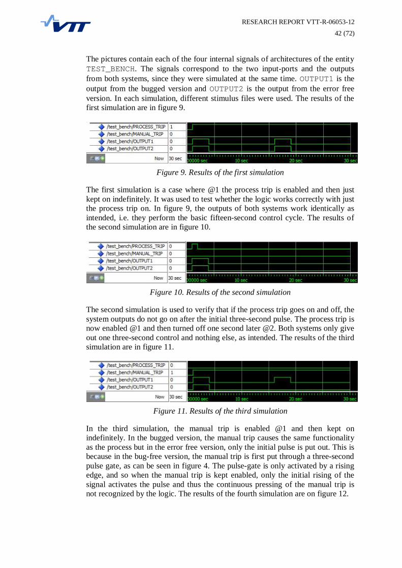
RESEARCH REPORT VTT-R-06053-12
42 (72)
The pictures contain each of the four internal signals of architectures of the entity TEST_BENCH. The signals correspond to the two input-ports and the outputs from both systems, since they were simulated at the same time. OUTPUT1 is the output from the bugged version and OUTPUT2 is the output from the error free version. In each simulation, different stimulus files were used. The results of the first simulation are in figure 9.
Figure 9. Results of the first simulation
The first simulation is a case where @1 the process trip is enabled and then just kept on indefinitely. It was used to test whether the logic works correctly with just the process trip on. In figure 9, the outputs of both systems work identically as intended, i.e. they perform the basic fifteen-second control cycle. The results of the second simulation are in figure 10.
Figure 10. Results of the second simulation
The second simulation is used to verify that if the process trip goes on and off, the system outputs do not go on after the initial three-second pulse. The process trip is now enabled @1 and then turned off one second later @2. Both systems only give out one three-second control and nothing else, as intended. The results of the third simulation are in figure 11.
Figure 11. Results of the third simulation
In the third simulation, the manual trip is enabled @1 and then kept on indefinitely. In the bugged version, the manual trip causes the same functionality as the process but in the error free version, only the initial pulse is put out. This is because in the bug-free version, the manual trip is first put through a three-second pulse gate, as can be seen in figure 4. The pulse-gate is only activated by a rising edge, and so when the manual trip is kept enabled, only the initial rising of the signal activates the pulse and thus the continuous pressing of the manual trip is not recognized by the logic. The results of the fourth simulation are on figure 12.
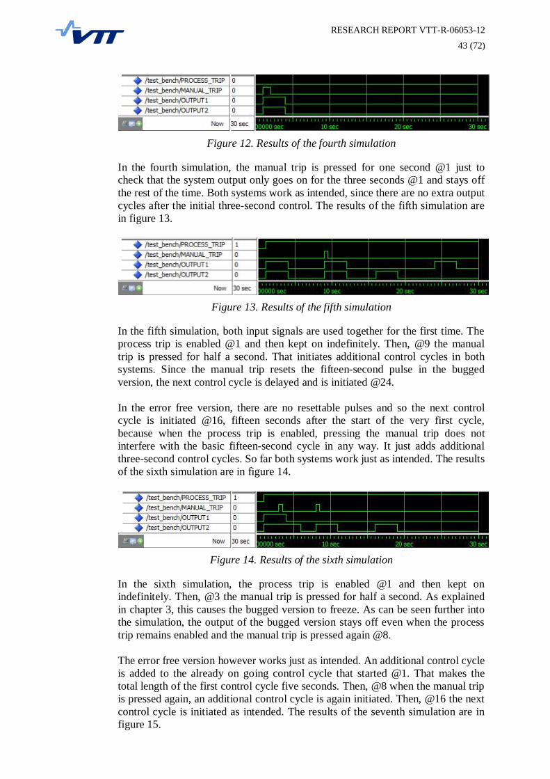
RESEARCH REPORT VTT-R-06053-12
43 (72)
Figure 12. Results of the fourth simulation
In the fourth simulation, the manual trip is pressed for one second @1 just to check that the system output only goes on for the three seconds @1 and stays off the rest of the time. Both systems work as intended, since there are no extra output cycles after the initial three-second control. The results of the fifth simulation are in figure 13.
Figure 13. Results of the fifth simulation
In the fifth simulation, both input signals are used together for the first time. The process trip is enabled @1 and then kept on indefinitely. Then, @9 the manual trip is pressed for half a second. That initiates additional control cycles in both systems. Since the manual trip resets the fifteen-second pulse in the bugged version, the next control cycle is delayed and is initiated @24. In the error free version, there are no resettable pulses and so the next control cycle is initiated @16, fifteen seconds after the start of the very first cycle, because when the process trip is enabled, pressing the manual trip does not interfere with the basic fifteen-second cycle in any way. It just adds additional three-second control cycles. So far both systems work just as intended. The results of the sixth simulation are in figure 14.
Figure 14. Results of the sixth simulation
In the sixth simulation, the process trip is enabled @1 and then kept on indefinitely. Then, @3 the manual trip is pressed for half a second. As explained in chapter 3, this causes the bugged version to freeze. As can be seen further into the simulation, the output of the bugged version stays off even when the process trip remains enabled and the manual trip is pressed again @8. The error free version however works just as intended. An additional control cycle is added to the already on going control cycle that started @1. That makes the total length of the first control cycle five seconds. Then, @8 when the manual trip is pressed again, an additional control cycle is again initiated. Then, @16 the next control cycle is initiated as intended. The results of the seventh simulation are in figure 15.
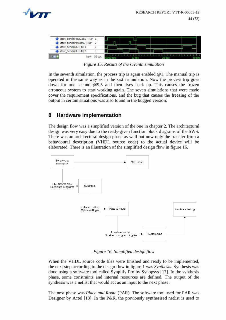
RESEARCH REPORT VTT-R-06053-12
44 (72)
Figure 15. Results of the seventh simulation
In the seventh simulation, the process trip is again enabled @1. The manual trip is operated in the same way as in the sixth simulation. Now the process trip goes down for one second @9,5 and then rises back up. This causes the frozen erroneous system to start working again. The seven simulations that were made cover the requirement specifications, and the bug that causes the freezing of the output in certain situations was also found in the bugged version.
8 Hardware implementation
The design flow was a simplified version of the one in chapter 2. The architectural design was very easy due to the ready-given function block diagrams of the SWS. There was an architectural design phase as well but now only the transfer from a behavioural description (VHDL source code) to the actual device will be elaborated. There is an illustration of the simplified design flow in figure 16.
Figure 16. Simplified design flow
When the VHDL source code files were finished and ready to be implemented, the next step according to the design flow in figure 1 was Synthesis. Synthesis was done using a software tool called Synplify Pro by Synopsys [17]. In the synthesis phase, some constraints and internal resources are defined. The output of the synthesis was a netlist that would act as an input to the next phase. The next phase was Place and Route (PAR). The software tool used for PAR was Designer by Actel [18]. In the P&R, the previously synthesised netlist is used to

RESEARCH REPORT VTT-R-06053-12
45 (72)
map the implementation of the logic for the particular device. The design is not yet transferred to the device in the PAR phase but the design is converted into detailed model of how the FPGA chip would be after the programming. In PAR, the I/O-ports of the VHDL design are now assigned to actual I/Oports of the FPGA chip. In this case, they were the clock signal, the switch-bank, the reset switch, and the LED-bank. The pins corresponding to the switches had to be manually assigned to the input ports of the design. This was done using I/O Attribute Editor of the Designer. The output of the PAR phase is the programming file that is used to configure the gates of the FPGA chip according to the design. The final phase was Programming. Programming was done using a software tool called FlashPro by Actel [19]. A connection between the PC and the FPGAs flash memory was formed using a USB cable. FlashPro was then used to erase the previous program from the FPGA’s memory, to transfer the new program in, and to verify the FPGA. Instantly after the program was transferred, the FPGA started to run it. As mentioned before, the biggest challenge was creating a synthesisable pulse gate in VHDL. Many versions were made and tested on the FPGA. As soon as the pulse gate started working as intended, the whole logic was put together by defining the structure in a top-level entity. Due to the limited input-interface, which consists of the 10 on-off switches and the reset button, only the cases that verify the correct functioning and the case where the bugged version freezes, were tested. The first switch of the switch-bank was connected to the process trip so that when the switch is on, the process trip is on. The reset button was connected to the manual trip so that it could be pressed like the actual button. The device performed as expected in all cases. It also froze when the manual trip was pressed during a control cycle when running the bugged version. Since the development kit contains a serial communication port, it is possible to do more comprehensive testing. Using the serial port requires an additional transceiver program to be designed which will be a part of an expanded case study.
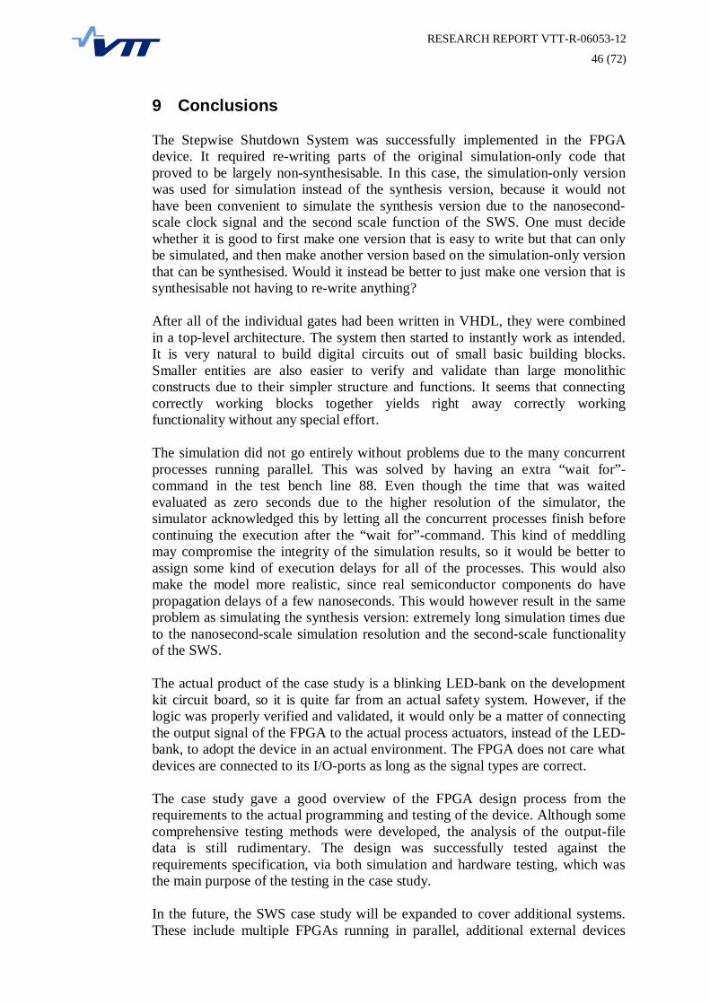
RESEARCH REPORT VTT-R-06053-12
46 (72)
9 Conclusions
The Stepwise Shutdown System was successfully implemented in the FPGA device. It required re-writing parts of the original simulation-only code that proved to be largely non-synthesisable. In this case, the simulation-only version was used for simulation instead of the synthesis version, because it would not have been convenient to simulate the synthesis version due to the nanosecond-scale clock signal and the second scale function of the SWS. One must decide whether it is good to first make one version that is easy to write but that can only be simulated, and then make another version based on the simulation-only version that can be synthesised. Would it instead be better to just make one version that is synthesisable not having to re-write anything? After all of the individual gates had been written in VHDL, they were combined in a top-level architecture. The system then started to instantly work as intended. It is very natural to build digital circuits out of small basic building blocks. Smaller entities are also easier to verify and validate than large monolithic constructs due to their simpler structure and functions. It seems that connecting correctly working blocks together yields right away correctly working functionality without any special effort. The simulation did not go entirely without problems due to the many concurrent processes running parallel. This was solved by having an extra “wait for”-command in the test bench line 88. Even though the time that was waited evaluated as zero seconds due to the higher resolution of the simulator, the simulator acknowledged this by letting all the concurrent processes finish before continuing the execution after the “wait for”-command. This kind of meddling may compromise the integrity of the simulation results, so it would be better to assign some kind of execution delays for all of the processes. This would also make the model more realistic, since real semiconductor components do have propagation delays of a few nanoseconds. This would however result in the same problem as simulating the synthesis version: extremely long simulation times due to the nanosecond-scale simulation resolution and the second-scale functionality of the SWS. The actual product of the case study is a blinking LED-bank on the development kit circuit board, so it is quite far from an actual safety system. However, if the logic was properly verified and validated, it would only be a matter of connecting the output signal of the FPGA to the actual process actuators, instead of the LED-bank, to adopt the device in an actual environment. The FPGA does not care what devices are connected to its I/O-ports as long as the signal types are correct. The case study gave a good overview of the FPGA design process from the requirements to the actual programming and testing of the device. Although some comprehensive testing methods were developed, the analysis of the output-file data is still rudimentary. The design was successfully tested against the requirements specification, via both simulation and hardware testing, which was the main purpose of the testing in the case study. In the future, the SWS case study will be expanded to cover additional systems. These include multiple FPGAs running in parallel, additional external devices

RESEARCH REPORT VTT-R-06053-12
47 (72)
such as sensors and a serial connection between a PC and the FPGA to be able to do more comprehensive testing.

RESEARCH REPORT VTT-R-06053-12
48 (72)
10 References
[1] Ranta, J., The Current State of FPGA Technology in the Nuclear
Domain. Espoo: VTT Technology 10, 2012, 62 p. ISBN 978-951-38-7622-7
[2] United States Nuclear Regulatory Commission (NRC), NUREG/CR-7006 Review Guidelines for Field-Programmable Gate Arrays in Nuclear Power Plant Safety Systems. USA: NRC, 2010, 94 p.
[3] European Space Agency (ESA), VHDL Modelling Guidelines. Netherlands: ESA, 1994, 50 p.
[4] Microsemi (Actel), IGLOO Low Power Flash FPGAs Datasheet,
Revision 21. 2012, 246 p.
[5] K. Björkman, J. Frits, J. Valkonen, K. Heljanko, I. Niemelä, Model-Based Analysis of a Stepwise Shutdown Logic - MODSAFE 2008 Work Report, VTT Working Papers 115, VTT Technical Research Centre of Finland, Espoo, Finland, March 2009, 42 p
[6] Smith, G. R., FPGAs 100, Everything You Need to Know to Get
Started. USA: Newnes, 2010, 245 p. ISBN: 978-1-85617-706-1.
[7] National Instruments, Introduction to FPGA Technology. 2012, http://www.ni.com/white-paper/6984/en (Referenced 6.9.2012).
[8] Bach, J., Tavolara I., Use of FPGA Technology in Implementation of the Logic of the Modernized Rod Control System (RCS) of the 900 MW EDF Fleet. Proceedings of NPIC&HMIT 2010, November 7-11, 2010, Las Vegas, Nevada. France: Rolls-Royce Civil Nuclear SAS, 2010, Pp. 1326-1336.
[9] Frequently Asked Questions and Answers, comp.lang.vhdl newsgroup
archive. 2004, http://www.vhdl.org/comp.lang.vhdl/FAQ1.html#synthesis, Referenced 30.08.2012.
[10] IEEE 1076-2008. IEEE Standard VHDL Language Reference Manual.
New York: IEEE, 2009, 640 p.
[11] IEEE 1076.6-2004. IEEE Standard for VHDL Register Transfer Level (RTL) Synthesis. New York: IEEE, 2004, 119 p.
[12] Mentor Graphics, ModelSim PE 10.0c, 2011. http://model.com
(referenced 6.9.2012).
[13] HDL Works, Scriptum, version 13.0 revision 1, 2012. http://www.hdlworks.com (referenced 6.9.2012).
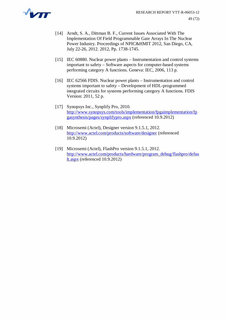
RESEARCH REPORT VTT-R-06053-12
49 (72)
[14] Arndt, S. A., Dittman B. F., Current Issues Associated With The Implementation Of Field Programmable Gate Arrays In The Nuclear Power Industry. Proceedings of NPIC&HMIT 2012, San Diego, CA, July 22-26, 2012. 2012, Pp. 1738-1745.
[15] IEC 60880. Nuclear power plants – Instrumentation and control systems
important to safety – Software aspects for computer-based systems performing category A functions. Geneva: IEC, 2006, 113 p.
[16] IEC 62566 FDIS. Nuclear power plants – Instrumentation and control
systems important to safety – Development of HDL-programmed integrated circuits for systems performing category A functions. FDIS Version: 2011, 52 p.
[17] Synopsys Inc., Synplify Pro, 2010.
http://www.synopsys.com/tools/implementation/fpgaimplementation/fpgasynthesis/pages/synplifypro.aspx (referenced 10.9.2012)
[18] Microsemi (Actel), Designer version 9.1.5.1, 2012.
http://www.actel.com/products/software/designer (referenced 10.9.2012)
[19] Microsemi (Actel), FlashPro version 9.1.5.1, 2012.
http://www.actel.com/products/hardware/program_debug/flashpro/default.aspx (referenced 10.9.2012)
RESEARCH REPORT VTT-R-06053-12
50 (72)
Appendix A: The simulation-only source code
------------------------------------------------------------ ------------------------------------------------------------ -- Designer : Lauri Lötjönen -- Company : VTT Technical Research Centre of Finland -- Date : 14.06.2012 -- Last Revised: 15.08.2012 ------------------------------------------------------------ -- 15.08.2012 : cleaning up for the pdf export ------------------------------------------------------------ -- A two-input AND-gate for simulation library ieee; use ieee.std_logic_1164.all; entity AND2GATE is port ( INPUT1 : in bit ; -- input 1: first operand (bit) INPUT2 : in bit ; -- input 2: second operand (bit) OUTPUT : out bit ); -- output: result of the operation (bit) end entity AND2GATE; architecture BEHAVIORAL of AND2GATE is begin -- the block is sensitive to both inputs process ( INPUT1, INPUT2 ) is begin OUTPUT <= INPUT1 and INPUT2; end process; end architecture; ------------------------------------------------------------ ------------------------------------------------------------ -- Designer : Lauri Lötjönen -- Company : VTT Technical Research Centre of Finland -- Date : 14.06.2012 -- Last Revised: 15.08.2012 ------------------------------------------------------------ -- 15.08.2012 : cleaning up for the pdf export ------------------------------------------------------------ -- A two-input OR-gate for simulation library ieee; use ieee.std_logic_1164.all; entity OR2GATE is port ( INPUT1 : in bit ; -- input 1: first operand (bit) INPUT2 : in bit ; -- input 2: second operand (bit) OUTPUT : out bit ); -- output: result of the operation (bit) end entity; architecture BEHAVIORAL of OR2GATE is begin process ( INPUT1, INPUT2 ) is begin OUTPUT <= INPUT1 or INPUT2; end process;
RESEARCH REPORT VTT-R-06053-12
51 (72)
end architecture; ------------------------------------------------------------ ------------------------------------------------------------ -- Designer : Lauri Lötjönen -- Company : VTT Technical Research Centre of Finland -- Date : 14.06.2012 -- Last Revised: 15.08.2012 ------------------------------------------------------------ -- 15.08.2012 : cleaning up for the pdf export ------------------------------------------------------------ -- An inverter for simulation library ieee; use ieee.std_logic_1164.all; entity INVERTER is port ( INPUT : in bit ; -- input: the invertee (bit) OUTPUT : out bit ); -- output: the inverse of the input (bit) end entity; architecture BEHAVIORAL of INVERTER is begin process ( INPUT ) is begin -- the inverse of the input is assigned to the output if INPUT = '0' then OUTPUT <= '1'; else OUTPUT <= '0'; end if; end process; end architecture; ------------------------------------------------------------ ------------------------------------------------------------ -- Designer : Lauri Lötjönen -- Company : VTT Technical Research Centre of Finland -- Date : 14.06.2012 -- Last Revised: 10.08.2012 ------------------------------------------------------------ ------------------------------------------------------------ -- A non-resettable pulse-gate for simulation entity PULSE is generic ( PULSE_LENGTH : time ); -- this conveys the pulse length (time) port ( INPUT : in bit ; -- input of the gate (bit) OUTPUT : out bit ); -- output of the gate (bit) end entity; -- the behavioral architecture architecture BEHAVIORAL of PULSE is begin
RESEARCH REPORT VTT-R-06053-12
52 (72)
process is begin -- rising edge of the input initiates the pulse while INPUT'event and INPUT = '1' loop OUTPUT <= '1'; -- output at 1 until enough time has passed wait for PULSE_LENGTH; -- this statement is non-syntesizable -- even if the input remains at 1 after the pulse, output goes to zero -- as specified. after this the "while" loop starts over. OUTPUT <= '0'; end loop; wait on INPUT; -- the process activates when there's an event on INPUT end process; end architecture; ------------------------------------------------------------ ------------------------------------------------------------ -- Designer : Lauri Lötjönen -- Company : VTT Technical Research Centre of Finland -- Date : 14.06.2012 -- Last Revised: 15.08.2012 ------------------------------------------------------------ -- 15.08.2012 : cleaning up for the pdf export ------------------------------------------------------------ -- A resettable pulse-gate for simulation library ieee; use ieee.std_logic_1164.all; entity PULSE_RESET is generic ( PULSE_LENGTH : time ); -- length of the pulse (time) port ( INPUT : in bit ; -- input 1: initiates the pulse (bit) RESET : in bit ; -- input 2: resets the timer (bit) OUTPUT : out bit ); -- output: the pulse itself (bit) end entity; -- the behavioral architecture architecture BEHAVIORAL of PULSE_RESET is begin -- no sensitivity list here because if there are wait-statements, -- the sensitivity list must be written as on the line 42 process is begin -- rising edge of the input initiates the timed action while INPUT'event and INPUT = '1' loop -- output at 1 until reset goes 1 or enough time has passed OUTPUT <= '1';
RESEARCH REPORT VTT-R-06053-12
53 (72)
-- rising edge of the input initiates the reset functionality -- this "wait"-statement is non-syntesizable wait until RESET'event and RESET = '1' for PULSE_LENGTH; -- OUTPUT goes 0 if reset is enabled or the pulse ends OUTPUT <= '0'; end loop; wait on INPUT; -- the process is activated by INPUT end process; end architecture; ------------------------------------------------------------ ------------------------------------------------------------ -- Designer : Lauri Lötjönen -- Company : VTT Technical Research Centre of Finland -- Date : 14.06.2012 -- Last Revised: 15.08.2012 ------------------------------------------------------------ -- 30.07.2012 : added the output generator -- 01.08.2012 : added the propagation delays -- 10.08.2012 : removed the prop delays from this version -- 15.08.2012 : cleaning up for the pdf export ------------------------------------------------------------ -- The Stepwise Shutdown system (SWS) logic circuit for simulation -- here are both the bugged and bug free versions of the circuit. library ieee; use ieee.std_logic_1164.all; entity SWS is -- the IO-ports of the SWS-logic structure port ( PROCESS_TRIP : in bit ; -- input: process alarms (bit) MANUAL_TRIP : in bit ; -- input: manual trip (bit) OUTPUT : out bit ); -- output: SWS actuation (bit) end entity; ------------------- the bugged version of the SWS -------------------------- architecture BUG of SWS is -- these are the internal signals used in the logical structure signal OR_OUT : bit; -- output of the OR-block (bit) signal AND_OUT : bit; -- output of the AND-block (bit) signal PULSE15_OUT : bit; -- output of the 15-second pulse (bit) signal PULSE15_NOUT : bit; -- PULSE15_OUT inverted (bit) signal PULSE3_OUT : bit; -- output of the 3-second pulse (bit) begin -- the blocks are connected according to the SWS schematic OUTPUT <= PULSE3_OUT; OR_GATE : entity work.OR2GATE(BEHAVIORAL)
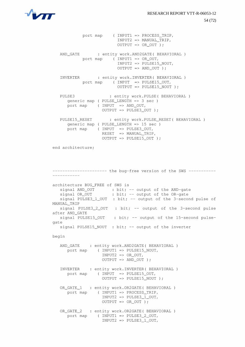
RESEARCH REPORT VTT-R-06053-12
54 (72)
port map ( INPUT1 => PROCESS_TRIP, INPUT2 => MANUAL_TRIP, OUTPUT => OR_OUT ); AND_GATE : entity work.AND2GATE( BEHAVIORAL ) port map ( INPUT1 => OR_OUT, INPUT2 => PULSE15_NOUT, OUTPUT => AND_OUT ); INVERTER : entity work.INVERTER( BEHAVIORAL ) port map ( INPUT => PULSE15_OUT, OUTPUT => PULSE15_NOUT ); PULSE3 : entity work.PULSE( BEHAVIORAL ) generic map ( PULSE_LENGTH => 3 sec ) port map ( INPUT => AND_OUT, OUTPUT => PULSE3_OUT ); PULSE15_RESET : entity work.PULSE_RESET( BEHAVIORAL ) generic map ( PULSE_LENGTH => 15 sec ) port map ( INPUT => PULSE3_OUT, RESET => MANUAL_TRIP, OUTPUT => PULSE15_OUT ); end architecture; ---------------------- the bug-free version of the SWS ---------------------- architecture BUG_FREE of SWS is signal AND_OUT : bit; -- output of the AND-gate signal OR_OUT : bit; -- output of the OR-gate signal PULSE3_1_OUT : bit; -- output of the 3-second pulse of MANUAL_TRIP signal PULSE3_2_OUT : bit; -- output of the 3-second pulse after AND_GATE signal PULSE15_OUT : bit; -- output of the 15-second pulse-gate signal PULSE15_NOUT : bit; -- output of the inverter begin AND_GATE : entity work.AND2GATE( BEHAVIORAL ) port map ( INPUT1 => PULSE15_NOUT, INPUT2 => OR_OUT, OUTPUT => AND_OUT ); INVERTER : entity work.INVERTER( BEHAVIORAL ) port map ( INPUT => PULSE15_OUT, OUTPUT => PULSE15_NOUT ); OR_GATE_1 : entity work.OR2GATE( BEHAVIORAL ) port map ( INPUT1 => PROCESS_TRIP, INPUT2 => PULSE3_1_OUT, OUTPUT => OR_OUT ); OR_GATE_2 : entity work.OR2GATE( BEHAVIORAL ) port map ( INPUT1 => PULSE3_2_OUT, INPUT2 => PULSE3_1_OUT,
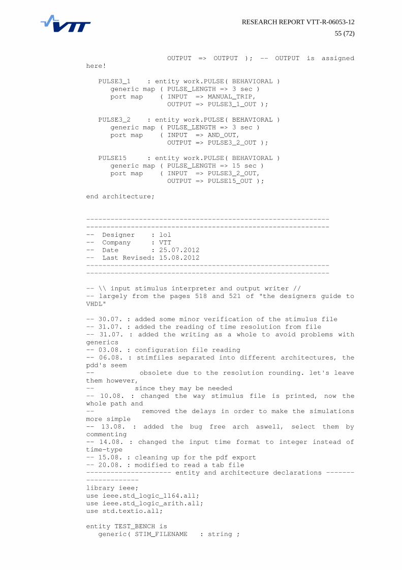
RESEARCH REPORT VTT-R-06053-12
55 (72)
OUTPUT => OUTPUT ); -- OUTPUT is assigned here! PULSE3_1 : entity work.PULSE( BEHAVIORAL ) generic map ( PULSE_LENGTH => 3 sec ) port map ( INPUT => MANUAL_TRIP, OUTPUT => PULSE3_1_OUT ); PULSE3_2 : entity work.PULSE( BEHAVIORAL ) generic map ( PULSE_LENGTH => 3 sec ) port map ( INPUT => AND_OUT, OUTPUT => PULSE3_2_OUT ); PULSE15 : entity work.PULSE( BEHAVIORAL ) generic map ( PULSE_LENGTH => 15 sec ) port map ( INPUT => PULSE3_2_OUT, OUTPUT => PULSE15_OUT ); end architecture; ------------------------------------------------------------ ------------------------------------------------------------ -- Designer : lol -- Company : VTT -- Date : 25.07.2012 -- Last Revised: 15.08.2012 ------------------------------------------------------------ ------------------------------------------------------------ -- \\ input stimulus interpreter and output writer // -- largely from the pages 518 and 521 of "the designers guide to VHDL" -- 30.07. : added some minor verification of the stimulus file -- 31.07. : added the reading of time resolution from file -- 31.07. : added the writing as a whole to avoid problems with generics -- 03.08. : configuration file reading -- 06.08. : stimfiles separated into different architectures, the pdd's seem -- obsolete due to the resolution rounding. let's leave them however, -- since they may be needed -- 10.08. : changed the way stimulus file is printed, now the whole path and -- removed the delays in order to make the simulations more simple -- 13.08. : added the bug free arch aswell, select them by commenting -- 14.08. : changed the input time format to integer instead of time-type -- 15.08. : cleaning up for the pdf export -- 20.08. : modified to read a tab file --------------------- entity and architecture declarations -------------------- library ieee; use ieee.std_logic_1164.all; use ieee.std_logic_arith.all; use std.textio.all; entity TEST_BENCH is generic( STIM_FILENAME : string ;
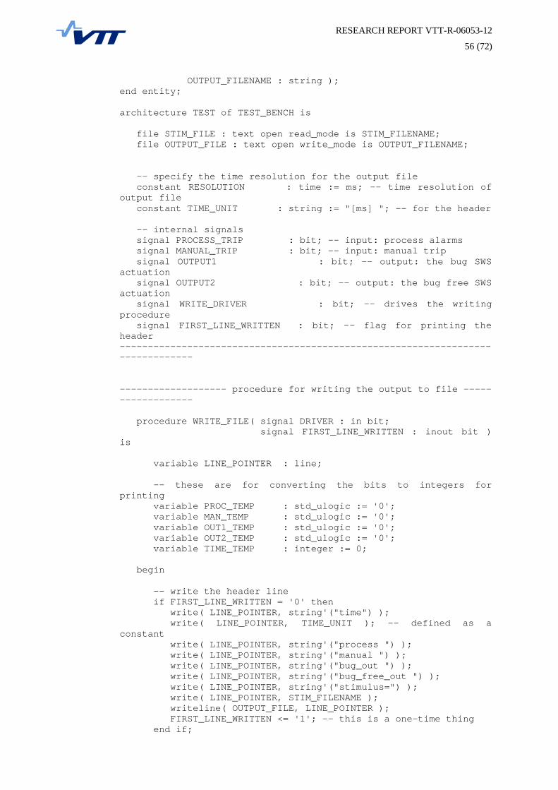
RESEARCH REPORT VTT-R-06053-12
56 (72)
OUTPUT_FILENAME : string ); end entity; architecture TEST of TEST_BENCH is file STIM_FILE : text open read_mode is STIM_FILENAME; file OUTPUT_FILE : text open write_mode is OUTPUT_FILENAME; -- specify the time resolution for the output file constant RESOLUTION : time := ms; -- time resolution of output file constant TIME_UNIT : string := "[ms] "; -- for the header -- internal signals signal PROCESS_TRIP : bit; -- input: process alarms signal MANUAL_TRIP : bit; -- input: manual trip signal OUTPUT1 : bit; -- output: the bug SWS actuation signal OUTPUT2 : bit; -- output: the bug free SWS actuation signal WRITE_DRIVER : bit; -- drives the writing procedure signal FIRST_LINE_WRITTEN : bit; -- flag for printing the header ------------------------------------------------------------------------------- ------------------- procedure for writing the output to file ------------------ procedure WRITE_FILE( signal DRIVER : in bit; signal FIRST_LINE_WRITTEN : inout bit ) is variable LINE_POINTER : line; -- these are for converting the bits to integers for printing variable PROC_TEMP : std_ulogic := '0'; variable MAN_TEMP : std_ulogic := '0'; variable OUT1_TEMP : std_ulogic := '0'; variable OUT2_TEMP : std_ulogic := '0'; variable TIME_TEMP : integer := 0; begin -- write the header line if FIRST_LINE_WRITTEN = '0' then write( LINE_POINTER, string'("time") ); write( LINE_POINTER, TIME_UNIT ); -- defined as a constant write( LINE_POINTER, string'("process ") ); write( LINE_POINTER, string'("manual ") ); write( LINE_POINTER, string'("bug_out ") ); write( LINE_POINTER, string'("bug_free_out ") ); write( LINE_POINTER, string'("stimulus=") ); write( LINE_POINTER, STIM_FILENAME ); writeline( OUTPUT_FILE, LINE_POINTER ); FIRST_LINE_WRITTEN <= '1'; -- this is a one-time thing end if;
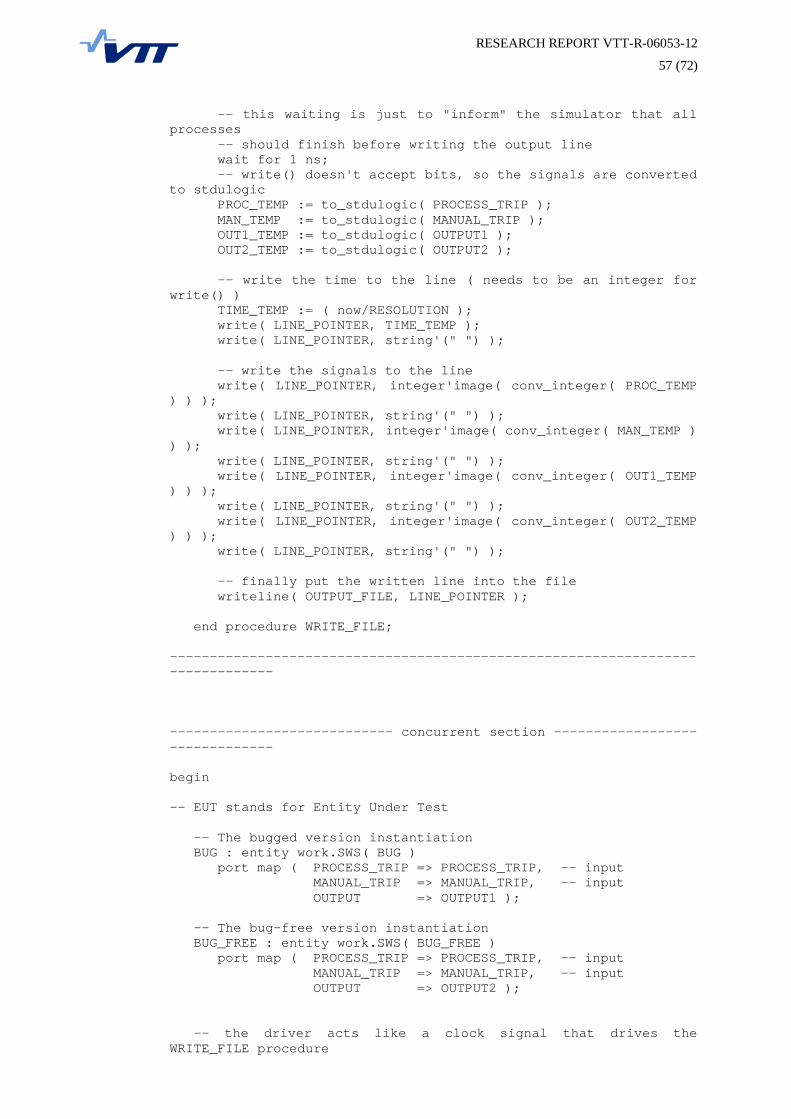
RESEARCH REPORT VTT-R-06053-12
57 (72)
-- this waiting is just to "inform" the simulator that all processes -- should finish before writing the output line wait for 1 ns; -- write() doesn't accept bits, so the signals are converted to stdulogic PROC_TEMP := to_stdulogic( PROCESS_TRIP ); MAN_TEMP := to_stdulogic( MANUAL_TRIP ); OUT1_TEMP := to_stdulogic( OUTPUT1 ); OUT2_TEMP := to_stdulogic( OUTPUT2 ); -- write the time to the line ( needs to be an integer for write() ) TIME_TEMP := ( now/RESOLUTION ); write( LINE_POINTER, TIME_TEMP ); write( LINE_POINTER, string'(" ") ); -- write the signals to the line write( LINE_POINTER, integer'image( conv_integer( PROC_TEMP ) ) ); write( LINE_POINTER, string'(" ") ); write( LINE_POINTER, integer'image( conv_integer( MAN_TEMP ) ) ); write( LINE_POINTER, string'(" ") ); write( LINE_POINTER, integer'image( conv_integer( OUT1_TEMP ) ) ); write( LINE_POINTER, string'(" ") ); write( LINE_POINTER, integer'image( conv_integer( OUT2_TEMP ) ) ); write( LINE_POINTER, string'(" ") ); -- finally put the written line into the file writeline( OUTPUT_FILE, LINE_POINTER ); end procedure WRITE_FILE; ------------------------------------------------------------------------------- ---------------------------- concurrent section ------------------------------- begin -- EUT stands for Entity Under Test -- The bugged version instantiation BUG : entity work.SWS( BUG ) port map ( PROCESS_TRIP => PROCESS_TRIP, -- input MANUAL_TRIP => MANUAL_TRIP, -- input OUTPUT => OUTPUT1 ); -- The bug-free version instantiation BUG_FREE : entity work.SWS( BUG_FREE ) port map ( PROCESS_TRIP => PROCESS_TRIP, -- input MANUAL_TRIP => MANUAL_TRIP, -- input OUTPUT => OUTPUT2 ); -- the driver acts like a clock signal that drives the WRITE_FILE procedure
RESEARCH REPORT VTT-R-06053-12
58 (72)
WRITE_DRIVER <= not WRITE_DRIVER after RESOLUTION; WRITE_FILE( WRITE_DRIVER, FIRST_LINE_WRITTEN ); ------------------------------------------------------------------------------- ------------------- process for reading the input files ----------------------- READ_INPUT : process is variable STIM_LINE : line; -- lines from stimfiles go here variable NEXT_TIME : time; -- time of next action variable TIME_INTEGER : integer := 0; -- from file variable PROCTRIP_FROMFILE : bit; -- process trip from the file variable MANTRIP_FROMFILE : bit; -- manual trip from the file variable STIM_LINE_NUM : natural; -- for reporting errors begin -- while loop for going through the stimulus file while not endfile( STIM_FILE ) loop -- keep track of the line number STIM_LINE_NUM := STIM_LINE_NUM + 1; -- take a line from the file readline( STIM_FILE, STIM_LINE ); -- time interpretation read( STIM_LINE, TIME_INTEGER ); -- convert integer to time for simulation NEXT_TIME := TIME_INTEGER*RESOLUTION; if NEXT_TIME >= 0 sec then -- process trip value interpretation read( STIM_LINE, PROCTRIP_FROMFILE ); -- read process trip value PROCESS_TRIP <= PROCTRIP_FROMFILE; -- assign it to the input port -- manual trip value interpretation read( STIM_LINE, MANTRIP_FROMFILE ); -- read manual trip value MANUAL_TRIP <= MANTRIP_FROMFILE; -- assign it to the input port -- wait until the simulation is at the specified time wait for NEXT_TIME; else report "ERROR: time value is invalid on line " & integer'image(STIM_LINE_NUM) & " of stimulus file"; PROCESS_TRIP <= '0';
RESEARCH REPORT VTT-R-06053-12
59 (72)
MANUAL_TRIP <= '0'; exit; -- if the input is invalid, reading is not continued end if; end loop; -- close the input file that has been read file_close( STIM_FILE ); wait; end process READ_INPUT; end architecture;

RESEARCH REPORT VTT-R-06053-12
60 (72)
Appendix B: The synthesis source code
------------------------------------------------------------ ------------------------------------------------------------ -- Designer : Lauri Lötjönen -- Company : VTT Technical Research Centre of Finland -- Date : 14.06.2012 -- Last Revised: 16.08.2012 ------------------------------------------------------------ -- 02.08. : added delays for simulation -- 16.08. : removed the delays and cleaned up for the pdf export ------------------------------------------------------------ -- A synthesizable two-input AND-gate library ieee; use ieee.std_logic_1164.all; entity AND2GATE is port ( CLK : in bit ; -- clock signal 48MHz INPUT1 : in bit ; -- input 1: first operand INPUT2 : in bit ; -- input 2: second operand OUTPUT : out bit ); -- output: result of the operation end entity AND2GATE; architecture BEHAVIORAL of AND2GATE is signal RESULT : bit; -- result is stored here before assigning to output begin process ( CLK, INPUT1, INPUT2 ) is begin -- the AND-operation is done on the rising edge of the clk signal if CLK'event and CLK = '1' then RESULT <= INPUT1 and INPUT2; end if; end process; -- after each clk cycle, the result is assigned to the output port OUTPUT <= RESULT; end architecture; ------------------------------------------------------------ ------------------------------------------------------------ -- Designer : Lauri Lötjönen -- Company : VTT Technical Research Centre of Finland -- Date : 14.06.2012 -- Last Revised: 16.08.2012 ------------------------------------------------------------ -- 02.08. : added delays for simulation -- 16.08. : removed the delays and cleaned up for the pdf export ------------------------------------------------------------ -- A synthesizable two-input OR-gate library ieee;
RESEARCH REPORT VTT-R-06053-12
61 (72)
use ieee.std_logic_1164.all; entity OR2GATE is port ( CLK : in bit ; -- clock signal 48MHz INPUT1 : in bit ; -- input 1: first operand INPUT2 : in bit ; -- input 2: second operand OUTPUT : out bit ); -- output: result of the operation end entity; architecture BEHAVIORAL of OR2GATE is signal RESULT : bit; -- result is stored here before assigning to output begin process ( CLK, INPUT1, INPUT2 ) is begin -- the OR-operation is done on the rising edge of the clk signal if CLK'event and CLK = '1' then RESULT <= INPUT1 or INPUT2; end if; end process; -- after each clk cycle, the result is assigned to the output port OUTPUT <= RESULT; end architecture; ------------------------------------------------------------ ------------------------------------------------------------ -- Designer : Lauri Lötjönen -- Company : VTT Technical Research Centre of Finland -- Date : 14.06.2012 -- Last Revised: 16.08.2012 ------------------------------------------------------------ -- 02.08. : added delays for simulation -- 16.08. : removed the delays and cleaned up for the pdf export ------------------------------------------------------------ -- A synthesizable inverter block library ieee; use ieee.std_logic_1164.all; entity INVERTER is port ( CLK : in bit ; -- clock signal 48MHz INPUT : in bit ; -- input: the invertee OUTPUT : out bit ); -- output: the inverse of the input end entity; architecture BEHAVIORAL of INVERTER is signal RESULT : bit; -- result is stored here before assigning to output begin process ( CLK, INPUT ) is begin -- the inversion is done on the rising edge of the clk signal if CLK'event and CLK = '1' then
RESEARCH REPORT VTT-R-06053-12
62 (72)
if INPUT = '0' then RESULT <= '1'; else RESULT <= '0'; end if; end if; end process; -- after each clk cycle, the result is assigned to the output port OUTPUT <= RESULT; end architecture; ------------------------------------------------------------ ------------------------------------------------------------ -- Designer : Lauri Lötjönen -- Company : VTT Technical Research Centre of Finland -- Date : 14.06.2012 -- Last Revised: 16.08.2012 ------------------------------------------------------------ -- 02.08. : added delays for simulation -- 16.08. : removed the delays and cleaned up for the pdf export ------------------------------------------------------------ -- A synthesizable non-resettable pulse-gate entity PULSE is -- the pulse length and time unit are conveyed from the top level entity generic ( PULSE_LENGTH : integer ; -- pulse lenghth, e.g. 3 sec TIME_UNIT : integer ); -- time unit in clock cycles -- there are 3 IO-ports: CLK, INPUT in; OUTPUT out port ( CLK : in bit ; -- clock signal 48MHz INPUT : in bit ; -- input of the gate OUTPUT : out bit ); -- output of the gate end entity; -- the only architecture is a behavioral description of the pulse block architecture BEHAVIORAL of PULSE is signal RESULT : bit; -- result is assigned here temporarily begin -- the block is activated by the clk signal and the input process ( CLK, INPUT ) is variable COUNTER : integer := 0; -- counter for the time delay variable PULSE_ON : bit; -- flag indicating pulse being on or off variable PREV_INPUT : bit; -- previous value of input begin -- everything happens on the rising edge of the clk signal if CLK'event and CLK = '1' then -- if current input is greater than the previous one, -- there's a rising edge which initializes the pulse if INPUT > PREV_INPUT then
RESEARCH REPORT VTT-R-06053-12
63 (72)
PULSE_ON := '1'; -- pulse is kept on for the duration of the pulse if COUNTER < PULSE_LENGTH*TIME_UNIT then RESULT <= '1'; COUNTER := COUNTER + 1; -- when time runs out, the pulse ends else RESULT <= '0'; PULSE_ON := '0'; COUNTER := 0; end if; -- if there is no rising edge but there is still time, -- pulse is continued elsif COUNTER < PULSE_LENGTH*TIME_UNIT and PULSE_ON = '1' then RESULT <= '1'; COUNTER := COUNTER + 1; else RESULT <= '0'; PULSE_ON := '0'; COUNTER := 0; end if; PREV_INPUT := INPUT; -- previous input saved for the next clk cycle end if; -- clk end process; -- after each clk cycle, the result is assigned to the output port OUTPUT <= RESULT; end architecture; ------------------------------------------------------------ ------------------------------------------------------------ -- Designer : Lauri Lötjönen -- Company : VTT Technical Research Centre of Finland -- Date : 14.06.2012 -- Last Revised: 16.08.2012 ------------------------------------------------------------ -- 02.08. : added delays for simulation -- 16.08. : removed the delays and cleaned up for the pdf export ------------------------------------------------------------ -- A synthesizable resettable pulse-gate library ieee; use ieee.std_logic_1164.all; entity PULSE_RESET is -- the pulse length and time unit are conveyed from the top level entity generic ( PULSE_LENGTH : integer ; -- pulse length (integer) in seconds TIME_UNIT : integer ); -- length of the time unit. e.g. 1 sec
RESEARCH REPORT VTT-R-06053-12
64 (72)
-- there are 4 IO-ports: CLK, INPUT, RESET in; OUTPUT out port ( CLK : in bit ; -- clock signal 48MHz INPUT : in bit ; -- input 1: initiates the pulse RESET : in bit ; -- input 2: resets the timer OUTPUT : out bit ); -- output: the pulse itself end entity; -- the behavioral architecture architecture BEHAVIORAL of PULSE_RESET is signal RESULT : bit; -- result is assigned here temporarily begin -- the block is activated by the clk signal, the input and the reset process (CLK, INPUT, RESET ) is variable COUNTER : integer := 0; -- counter for the time delay variable PULSE_ON : bit; -- flag indicating the pulse being on or off variable PREV_INPUT : bit; -- for detecting rising edge of the input variable PREV_RESET : bit; -- for detecting rising edge of the reset begin -- everything happens on the rising edge of the clk signal if CLK'event and CLK = '1' then -- if input is greater than the previous one, there's a rising edge if INPUT > PREV_INPUT then PULSE_ON := '1'; -- wait for appropriate time or the rising edge of reset if COUNTER < PULSE_LENGTH*TIME_UNIT and RESET <= PREV_RESET then RESULT <= '1'; COUNTER := COUNTER + 1; else RESULT <= '0'; PULSE_ON := '0'; COUNTER := 0; end if; -- if there isn't a rising edge on the input but the pulse has been -- initialized (PULSE_ON = '1'), and there's still time on timer, -- the pulse is continued until reset is pressed or the time runs out elsif COUNTER < PULSE_LENGTH*TIME_UNIT and PULSE_ON = '1' and RESET <= PREV_RESET then RESULT <= '1'; COUNTER := COUNTER + 1; else RESULT <= '0'; PULSE_ON := '0'; COUNTER := 0;
RESEARCH REPORT VTT-R-06053-12
65 (72)
end if; PREV_INPUT := INPUT; -- current input saved for the next clk cycle PREV_RESET := RESET; -- current reset saved for the next clk cycle end if; -- clk end process; -- after each clk cycle, the result is assigned to the output port OUTPUT <= RESULT; end architecture; ------------------------------------------------------------ ------------------------------------------------------------ -- Designer : Lauri Lötjönen -- Company : VTT Technical Research Centre of Finland -- Date : 03.07.2012 -- Last Revised: 16.08.2012 ------------------------------------------------------------ -- 02.08. : added delays for simulation -- 16.08. : removed the delays and cleaned up for the pdf export ------------------------------------------------------------ -- The synthesizable VHDL implementation of the Stepwise Shutdown system logic -- Included are both, the bugged and the bug-free, designs -- uncomment the architecture you wish to implement and comment the other one library ieee; use ieee.std_logic_1164.all; entity topLevel is -- there are 4 IO-ports in the overall system: -- inputs: clock, reset and the signal to the 10 switches -- outputs: the signal to the 10 leds port ( CLK : in bit; -- clock signal 48MHz RST_N : in bit; -- active low reset SWITCHES : in bit_vector(9 downto 0); -- 10 DIP switches LEDS : out bit_vector(9 downto 0) ); -- 10 leds on the board end entity; ------------------------------------------------------------------------------- -- THE BUG FREE ARCHITECTURE ------------------------------------------------------------------------------- -- comment/uncomment starting here
RESEARCH REPORT VTT-R-06053-12
66 (72)
architecture BUG_FREE of topLevel is -- the internal signals of the architecture signal AND_OUT : bit; -- output of the AND-gate signal OR_OUT : bit; -- output of the OR-gate signal PULSE3_1_OUT : bit; -- output of the 3-second pulse of MANUAL_TRIP signal PULSE3_2_OUT : bit; -- output of the 3-second pulse after AND_GATE signal PULSE15_OUT : bit; -- output of the 15-second pulse-gate signal PULSE15_NOUT : bit; -- output of the inverter signal PROCESS_TRIP : bit; -- input from the process signal MANUAL_TRIP : bit; -- input from the operator signal OUTPUT : bit; -- output of the system -- time delays are implemented using the clk frequency and counters constant SECOND : integer := 48000000; -- 48E6 clk cycles = 1 second -- the architecure uses components that are defined in different source files. -- here they are declared as components that can be used in the architecture -- declaration of the pulse gate component PULSE is generic( PULSE_LENGTH : integer ; TIME_UNIT : integer ); port( CLK : in bit ; INPUT : in bit ; OUTPUT : out bit ); end component; -- declaration of the 2-input AND-gate component AND2GATE is port( CLK : in bit ; INPUT1 : in bit ; INPUT2 : in bit ; OUTPUT : out bit ); end component; -- declaration of the inverter component INVERTER is port( CLK : in bit ; INPUT : in bit ; OUTPUT : out bit ); end component; -- declaration of the 2-input OR-gate component OR2GATE is port( CLK : in bit ; INPUT1 : in bit ; INPUT2 : in bit ; OUTPUT : out bit ); end component; begin -- the entity's IO-ports are connected to the architecure's internal signals
RESEARCH REPORT VTT-R-06053-12
67 (72)
PROCESS_TRIP <= SWITCHES(0); -- the first switch acts as the process input MANUAL_TRIP <= not RST_N; -- the reset acts as the operator input LEDS <= (others => OUTPUT); -- the leds indicate the output of the system -- now the design specific logic gates are created by creating instances of -- the predefined components and connecting them together using the internal -- signals. Thus the desired logic ciruit is obtained AND_GATE : component AND2GATE port map ( CLK => CLK, INPUT1 => PULSE15_NOUT, INPUT2 => OR_OUT, OUTPUT => AND_OUT ); INV_GATE : component INVERTER port map ( CLK => CLK, INPUT => PULSE15_OUT, OUTPUT => PULSE15_NOUT ); OR_GATE_1 : component OR2GATE port map ( CLK => CLK, INPUT1 => PROCESS_TRIP, INPUT2 => PULSE3_1_OUT, OUTPUT => OR_OUT ); OR_GATE_2 : component OR2GATE port map ( CLK => CLK, INPUT1 => PULSE3_2_OUT, INPUT2 => PULSE3_1_OUT, OUTPUT => OUTPUT ); PULSE3_1 : component PULSE generic map ( PULSE_LENGTH => 3, TIME_UNIT => SECOND ) port map ( CLK => CLK, INPUT => MANUAL_TRIP, OUTPUT => PULSE3_1_OUT ); PULSE3_2 : component PULSE generic map ( PULSE_LENGTH => 3, TIME_UNIT => SECOND ) port map ( CLK => CLK, INPUT => AND_OUT , OUTPUT => PULSE3_2_OUT ); PULSE15 : component PULSE generic map ( PULSE_LENGTH => 15, TIME_UNIT => SECOND ) port map ( CLK => CLK, INPUT => PULSE3_2_OUT, OUTPUT => PULSE15_OUT ); end architecture; -- comment/uncomment ending here
RESEARCH REPORT VTT-R-06053-12
68 (72)
------------------------------------------------------------------------------- -- THE BUGGED ARCHITECTURE ------------------------------------------------------------------------------- ---- comment/uncomment starting here -- --architecture BUG of topLevel is -- -- -- declaration of the non-resetable pulse gate -- component PULSE is -- generic( PULSE_LENGTH : integer ; -- TIME_UNIT : integer ); -- port( CLK : in bit ; -- INPUT : in bit ; -- OUTPUT : out bit ); -- end component; -- -- -- declaration of the resetable pulse gate -- component PULSE_RESET is -- generic( PULSE_LENGTH : integer ; -- TIME_UNIT : integer ); -- port( CLK : in bit ; -- INPUT : in bit ; -- RESET : in bit ; -- OUTPUT : out bit ); -- end component; -- -- -- declaration of the 2-input AND-gate -- component AND2GATE is -- port( CLK : in bit ; -- INPUT1 : in bit ; -- INPUT2 : in bit ; -- OUTPUT : out bit ); -- end component; -- -- -- declaration of the inverter gate -- component INVERTER is -- port( CLK : in bit ; -- INPUT : in bit ; -- OUTPUT : out bit ); -- end component; -- -- -- declaration of the 2-input OR-gate -- component OR2GATE is -- port( CLK : in bit ; -- INPUT1 : in bit ; -- INPUT2 : in bit ; -- OUTPUT : out bit ); -- end component; -- -- -- the internal signals of the architecture -- signal OR_OUT : bit; -- output of the OR-gate -- signal AND_OUT : bit; -- output of the AND-gate -- signal PULSE15_OUT : bit; -- output of the 15-second pulse -- signal PULSE15_NOUT : bit; -- PULSE15_OUT inverted -- signal PULSE3_OUT : bit; -- output of the 3-second pulse -- signal PROCESS_TRIP : bit; -- input from the process -- signal MANUAL_TRIP : bit; -- input from the operator -- -- -- time delays are implemented using the clk frequency and counters
RESEARCH REPORT VTT-R-06053-12
69 (72)
-- constant SECOND : integer := 48000000; -- 48E6 clk cycles = 1 second -- --begin -- -- -- the entity's IO-ports are connected to the architecure's internal signals -- -- PROCESS_TRIP <= SWITCHES(0); -- first switch acts as process input -- MANUAL_TRIP <= not RST_N; -- active low reset acts as operator input -- LEDS <= (others => PULSE3_OUT); -- leds indicate the output of the system -- -- now the system output is PULSE3_OUT -- -- -- -- now the design specific logic gates are created by creating instances of -- -- the predefined components and connecting them together using the internal -- -- signals. Thus the desired logic ciruit is obtained -- -- -- OR_GATE : component OR2GATE -- port map ( CLK => CLK, -- INPUT1 => PROCESS_TRIP, -- INPUT2 => MANUAL_TRIP, -- OUTPUT => OR_OUT ); -- -- AND_GATE : component AND2GATE -- port map ( CLK => CLK, -- INPUT1 => OR_OUT, -- INPUT2 => PULSE15_NOUT, -- OUTPUT => AND_OUT ); -- -- INV_GATE : component INVERTER -- port map ( CLK => CLK, -- INPUT => PULSE15_OUT, -- OUTPUT => PULSE15_NOUT ); -- -- PULSE3 : component PULSE -- generic map ( PULSE_LENGTH => 3, -- TIME_UNIT => SECOND ) -- port map ( CLK => CLK, -- INPUT => AND_OUT, -- OUTPUT => PULSE3_OUT ); -- -- PULSE15_RESET : component PULSE_RESET -- generic map ( PULSE_LENGTH => 15, -- TIME_UNIT => SECOND ) -- port map ( CLK => CLK, -- INPUT => PULSE3_OUT, -- RESET => MANUAL_TRIP, -- OUTPUT => PULSE15_OUT ); -- --end architecture; -- ---- comment/uncomment ending here
RESEARCH REPORT VTT-R-06053-12
70 (72)
Appendix C: The Tcl source code for the SWSim interface
## author: lol ## company: VTT ## date: 14.08.2012 ## last revised: 23.08.2012 ## A command prompt interface for running ModelSim simulations for the ## Stepwise Shutdown system # to check if there's a / in the end. if omitted, it will be added proc check_slash directory { # take the length of the given pathname set dir_length [string length $directory] if { [string index $directory end ] ne "/"} { return "$directory/" } else { return $directory } } ## the header prints puts "" puts "- Welcome to SWSim: the simulation interface for the Stepwise Shutdown system!" puts "- Version 1.0 (13.08.2012) by Lauri Lötjönen\n" puts "Instructions:" puts " -Give full paths for the directories and use / instead of \\ as the separator." puts " -If you want to exit the simulation, type quit and press enter." puts "" ## get the project directory that contains the source files while true { # print the query for source file directory puts -nonewline "Source file directory:\n> " # take the dir from the user input gets stdin project_filepath; puts -nonewline "" #check that there is no \ as separator if {[string index $project_filepath 2] eq "\\"} { puts "\nERROR: Use / instead of \\\n" continue } # if quit was typed, quit if {$project_filepath eq "quit"} { quit # check that the given directory exists } elseif {$project_filepath eq ""} { continue } elseif {[file isdirectory $project_filepath]} { # add a / if omitted form the dir path set project_filepath [check_slash $project_filepath]; puts -nonewline "" #check whether the dir has the source files (.vhd files) if {[ catch {glob $project_filepath\*.vhd} ]} { puts "\nERROR: Cannot find source files!\n"
RESEARCH REPORT VTT-R-06053-12
71 (72)
continue } # take the source files from the directory set source_files [glob $project_filepath\*.vhd]; puts -nonewline "" puts "" break } else { puts "\nERROR: Invalid directory!\n" } } ## get the stimulus file directory while true { # print the query for stimulus file directory puts -nonewline "Stimulus file directory:\n> " # take the dir from the user input gets stdin stim_filepath; puts -nonewline "" #check that there is no \ as separator if {[string index $stim_filepath 2] eq "\\"} { puts "\nERROR: use / instead of \ !" continue } # if quit was typed, quit the simulation if {$stim_filepath eq "quit"} { quit # check that the given directory exists } elseif {$stim_filepath eq ""} { continue } elseif {[file isdirectory $stim_filepath]} { # add / to the path if omitted set stim_filepath [check_slash $stim_filepath]; puts -nonewline "" # take the files from the dir if {[ catch {glob $stim_filepath\*.tab} ]} { puts "Cannot find stimulus files!\n" continue } set stimfiles [glob $stim_filepath\*.tab]; puts -nonewline "" # sort the stimfiles list properly set stimfiles [lsort -dictionary $stimfiles]; puts "" break } else { puts "\nERROR: Invalid directory!\n" } } ## get the output directory and create it if necessary while true { puts -nonewline "Output file directory (will be created if doesn't exist): \n> " # take the dir from user input gets stdin output_filepath; puts -nonewline "" # if no dir was given, give the error message if {$output_filepath eq ""} { continue } file mkdir $output_filepath; if {$output_filepath eq "quit"} {
RESEARCH REPORT VTT-R-06053-12
72 (72)
quit } elseif {$output_filepath eq ""} { continue } else { set output_filepath [check_slash $output_filepath]; puts "" break } } ## get the simulation time and add time unit if necessary (sec is the default) puts -nonewline "Simulation time (e.g. 20 sec):\n> " gets stdin simulation_time; puts -nonewline "" if {$simulation_time eq "quit"} { quit } elseif {[string is double $simulation_time]} { set simulation_time "$simulation_time sec\n"; puts ""; } elseif {$simulation_time eq ""} { continue } # print all the gathered information before the simulation puts "\nParameters ready. Press enter to start simulation." gets stdin; puts "Starting simulation...\n" # create the working library #set library_name kirjasto; puts -nonewline "" #vlib $project_name set project_name projekti; puts -nonewline "" project new $project_filepath\$project_name $project_name set i 0; puts -nonewline "" # add the files to the project and compile them foreach i $source_files { project addfile $i vcom -quiet $i } # the simulation is initiated here set i 0; puts -nonewline "" set j 1; puts -nonewline "" foreach i $stimfiles { vsim -quiet -gSTIM_FILENAME="$i" -GOUTPUT_FILENAME="$output_filepath\output$j.txt" TEST_BENCH run $simulation_time incr j } # delete the project file, since it is no longer needed project delete $project_name set j 1; puts "" puts "Simulation complete! View the results at $output_filepath\n" puts "Press enter to exit" gets stdin quit