Embed Size (px)
Citation preview

Freescale SemiconductorData Sheet: Advance Information
Document Number: MPC5646CRev.6, 02/2014
© Freescale Semiconductor, Inc., 2009-2014. All rights reserved.
This document contains information on a product under development. Freescale reserves the right to change or discontinue this product without notice.
MPC5646C
TBD
MAPBGA–22515 mm x 15 mm
QFN12##_mm_x_##mm
SOT-343R##_mm_x_##mm
PKG-TBD## mm x ## mm
256 MAPBGA(17 mm x 17 mm)
208-pin LQFP(28 mm x 28 mm)
176-pin LQFP(24 mm x 24 mm)
On-chip modules available within the family include the following features:
• e200z4d dual issue, 32-bit core Power Architecture compliant CPU
— Up to 120 MHz
— 4 KB, 2/4-Way Set Associative Instruction Cache
— Variable length encoding (VLE)
— Embedded floating-point (FPU) unit
— Supports Nexus3+
• e200z0h single issue, 32-bit core Power Architecture compliant CPU
— Up to 80 MHz
— Variable length encoding (VLE)
— Supports Nexus3+
• Up to 3 MB on-chip flash memory: flash page buffers to improve access time
• Up to 256 KB on-chip SRAM
• 64 KB on-chip data flash memory to support EEPROM emulation
• Up to 16 semaphores across all slave ports
• User selectable MBIST
• Low-power modes supported: STOP, HALT, STANDBY
• 16 region Memory Protection Unit (MPU)
• Dual-core Interrupt Controller (INTC). Interrupt sources can be routed to
MPC5646CMicrocontroller Data Sheet
e200z4d, e200z0h, or both.• Crossbar switch architecture for concurrent
access to peripherals, flash memory, and SRAM from multiple bus masters
• 32 channel eDMA controller with DMAMUX
• Timer supports input/output channels providing 16-bit input capture, output compare, and PWM functions (eMIOS)
• 2 analog-to-digital converters (ADC): one 10-bit and one 12-bit
• Cross Trigger Unit (CTU) to enable synchronization of ADC conversions with a timer event from the eMIOS or from the PIT
• Up to 8 serial peripheral interface (DSPI) modules
• Up to 10 serial communication interface (LINFlex) modules
• Up to 6 full CAN (FlexCAN) modules with 64 MBs each
• CAN Sampler to catch ID of CAN message
• 1 inter IC communication interface (I2C) module
• Up to 177 (LQFP) or 199 (BGA) configurable general purpose I/O pins
• 1 System Timer Module (STM) with four 32-bit compare channels
• Up to 8 periodic interrupt timers (PIT) with 32-bit counter resolution

MPC5646C Data Sheet, Rev.6
Freescale Semiconductor2
Table of ContentsIntroduction . . . . . . . . . . . . . . . . . . . . . . . . . . . . . . . . . . . . . . . .41.1 Document Overview . . . . . . . . . . . . . . . . . . . . . . . . . . . .41.2 Description . . . . . . . . . . . . . . . . . . . . . . . . . . . . . . . . . . .4
2 Block diagram . . . . . . . . . . . . . . . . . . . . . . . . . . . . . . . . . . . . . .73 Package pinouts and signal descriptions . . . . . . . . . . . . . . . .10
3.1 Pad types . . . . . . . . . . . . . . . . . . . . . . . . . . . . . . . . . . .133.2 System pins . . . . . . . . . . . . . . . . . . . . . . . . . . . . . . . . .143.3 Functional ports . . . . . . . . . . . . . . . . . . . . . . . . . . . . . .14
4 Electrical Characteristics . . . . . . . . . . . . . . . . . . . . . . . . . . . .414.1 Parameter classification . . . . . . . . . . . . . . . . . . . . . . . .414.2 NVUSRO register . . . . . . . . . . . . . . . . . . . . . . . . . . . . .41
4.2.1 NVUSRO [PAD3V5V(0)] field description . . . . .424.2.2 NVUSRO [PAD3V5V(1)] field description . . . . .42
4.3 Absolute maximum ratings . . . . . . . . . . . . . . . . . . . . . .424.4 Recommended operating conditions . . . . . . . . . . . . . .444.5 Thermal characteristics. . . . . . . . . . . . . . . . . . . . . . . . .47
4.5.1 Package thermal characteristics . . . . . . . . . . . .474.5.2 Power considerations. . . . . . . . . . . . . . . . . . . . .48
4.6 I/O pad electrical characteristics . . . . . . . . . . . . . . . . . .484.6.1 I/O pad types . . . . . . . . . . . . . . . . . . . . . . . . . . .484.6.2 I/O input DC characteristics. . . . . . . . . . . . . . . .494.6.3 I/O output DC characteristics. . . . . . . . . . . . . . .504.6.4 Output pin transition times. . . . . . . . . . . . . . . . .524.6.5 I/O pad current specification . . . . . . . . . . . . . . .53
4.7 RESET electrical characteristics. . . . . . . . . . . . . . . . . .554.8 Power management electrical characteristics. . . . . . . .57
4.8.1 Voltage regulator electrical characteristics . . . .574.8.2 VDD_BV options . . . . . . . . . . . . . . . . . . . . . . . .594.8.3 Voltage monitor electrical characteristics. . . . . .60
4.9 Low voltage domain power consumption . . . . . . . . . . .614.10 Flash memory electrical characteristics . . . . . . . . . . . .63
4.10.1 Program/Erase characteristics. . . . . . . . . . . . . .634.10.2 Flash memory power supply DC characteristics654.10.3 Flash memory start-up/switch-off timings . . . . .66
4.11 Electromagnetic compatibility (EMC) characteristics . .664.11.1 Designing hardened software to avoid noise
problems. . . . . . . . . . . . . . . . . . . . . . . . . . . . . . 664.11.2 Electromagnetic interference (EMI) . . . . . . . . . 674.11.3 Absolute maximum ratings (electrical sensitivity)67
4.12 Fast external crystal oscillator (4–40 MHz) electrical characteristics . . . . . . . . . . . . . . . . . . . . . . . . . . . . . . . 68
4.13 Slow external crystal oscillator (32 kHz) electrical characteristics . . . . . . . . . . . . . . . . . . . . . . . . . . . . . . . 71
4.14 FMPLL electrical characteristics . . . . . . . . . . . . . . . . . 734.15 Fast internal RC oscillator (16 MHz) electrical
characteristics . . . . . . . . . . . . . . . . . . . . . . . . . . . . . . . 744.16 Slow internal RC oscillator (128 kHz) electrical
characteristics . . . . . . . . . . . . . . . . . . . . . . . . . . . . . . . 754.17 ADC electrical characteristics . . . . . . . . . . . . . . . . . . . 76
4.17.1 Introduction . . . . . . . . . . . . . . . . . . . . . . . . . . . 764.18 Fast Ethernet Controller . . . . . . . . . . . . . . . . . . . . . . . 87
4.18.1 MII Receive Signal Timing (RXD[3:0], RX_DV, RX_ER, and RX_CLK) . . . . . . . . . . . . . . . . . . . 87
4.18.2 MII Transmit Signal Timing (TXD[3:0], TX_EN, TX_ER, TX_CLK). . . . . . . . . . . . . . . . . . . . . . . 87
4.18.3 MII Async Inputs Signal Timing (CRS and COL)884.18.4 MII Serial Management Channel Timing (MDIO and
MDC)894.19 On-chip peripherals . . . . . . . . . . . . . . . . . . . . . . . . . . . 91
4.19.1 Current consumption . . . . . . . . . . . . . . . . . . . . 914.19.2 DSPI characteristics. . . . . . . . . . . . . . . . . . . . . 934.19.3 Nexus characteristics . . . . . . . . . . . . . . . . . . . 1014.19.4 JTAG characteristics. . . . . . . . . . . . . . . . . . . . 103
5 Package characteristics. . . . . . . . . . . . . . . . . . . . . . . . . . . . 1055.1 Package mechanical data . . . . . . . . . . . . . . . . . . . . . 105
5.1.1 176 LQFP package mechanical drawing . . . . 1055.1.2 208 LQFP package mechanical drawing . . . . 1085.1.3 256 MAPBGA package mechanical drawing . 113
6 Ordering information . . . . . . . . . . . . . . . . . . . . . . . . . . . . . . 1157 Revision history. . . . . . . . . . . . . . . . . . . . . . . . . . . . . . . . . . 116

Other Features
• System clocks sources
— 4–40 MHz external crystal oscillator
— 16 MHz internal RC oscillator
— FMPLL
— Additionally, there are two low power oscillators: 128 kHz internal RC oscillator, 32 kHz external crystal oscillator
• Real Time Counter (RTC) with clock source from internal 128 kHz or 16 MHz oscillators or external 4–40 MHz crystal
— Supports autonomous wake-up with 1 ms resolution with max timeout of 2 seconds
— Optional support from external 32 kHz crystal oscillator, supporting wake-up with 1 second resolution and max timeout of 1 hour
• 1 Real Time Interrupt (RTI) with 32-bit counter resolution
• 1 Safety Enhanced Software Watchdog Timer (SWT) that supports keyed functionality
• 1 dual-channel FlexRay Controller with 128 message buffers
• 1 Fast Ethernet Controller (FEC)
• On-chip voltage regulator (VREG)
• Cryptographic Services Engine (CSE)
• Offered in the following standard package types:
— 176-pin LQFP, 24 24 mm, 0.5 mm Lead Pitch
— 208-pin LQFP, 28 28 mm, 0.5 mm Lead Pitch
— 256-ball MAPBGA, 17 17mm, 1.0 mm Lead Pitch
MPC5646C Data Sheet, Rev.6
Freescale Semiconductor 3

Introduction
1 Introduction
1.1 Document OverviewThis document describes the features of the family and options available within the family members, and highlights important electrical and physical characteristics of the MPC5646C device. To ensure a complete understanding of the device functionality, refer also to the MPC5646C Reference Manual.
1.2 DescriptionThe MPC5646C is a new family of next generation microcontrollers built on the Power Architecture embedded category. This document describes the features of the family and options available within the family members, and highlights important electrical and physical characteristics of the device.
The MPC5646C family expands the range of the MPC560xB microcontroller family. It provides the scalability needed to implement platform approaches and delivers the performance required by increasingly sophisticated software architectures. The advanced and cost-efficient host processor core of the MPC5646C automotive controller family complies with the Power Architecture embedded category, which is 100 percent user-mode compatible with the original Power Architecture user instruction set architecture (UISA). It operates at speeds of up to 120 MHz and offers high performance processing optimized for low power consumption. It also capitalizes on the available development infrastructure of current Power Architecture devices and is supported with software drivers, operating systems and configuration code to assist with users implementations.
MPC5646C Data Sheet, Rev.6
Freescale Semiconductor4

Intro
du
ction
F
5646B MPC5646C
208LQFP
176LQFP
208LQFP
256BGA
0z4d e200z4d + e200z0h
20 MHz 0z4d)
Up to 120 MHz (e200z4d)
Up to 80 MHz (e200z0h)3
3 MB
2 KB 256 KB
33 ch 27 ch 33 ch
10 ch 5 ch 10 ch
MP
C5646C
Data S
heet, R
ev.6
reescale Sem
iconductor 5
Table 1. MPC5646C family comparison1
Feature MPC5644B MPC5644C MPC5645B MPC5645C MPC
Package 176LQFP
208LQFP
176LQFP
208LQFP
256BGA
176LQFP
208LQFP
176LQFP
208LQFP
256BGA
176LQFP
CPU e200z4d e200z4d + e200z0h e200z4d e200z4d + e200z0h e20
Execution speed2 Up to 120 MHz (e200z4d)
Up to 120 MHz (e200z4d)
Up to 80 MHz (e200z0h)3
Up to 120 MHz (e200z4d)
Up to 120 MHz (e200z4d)
Up to 80 MHz (e200z0h)3
Up to 1(e20
Code flash memory 1.5 MB 2 MB
Data flash memory 4 x16 KB
SRAM 128 KB 192 KB 160 KB 256 KB 19
MPU 16-entry
eDMA4 32 ch
10-bit ADC
27 ch 33 ch 27 ch 33 ch 27 ch 33 ch 27 ch 33 ch 27 chdedicated5,6
shared with12-bit ADC7 19 ch
12-bit ADC
5 ch 10 ch 5 ch 10 ch 5 ch 10 ch 5 ch 10 ch 5 chdedicated8
shared with10-bit ADC7 19 ch
CTU 64 ch
Total timer I/O9 eMIOS 64 ch, 16-bit
SCI (LINFlexD) 10
SPI (DSPI) 8
CAN (FlexCAN)10 6
FlexRay Yes
STCU11 Yes

Intro
du
ction
6
o Yes
177 147 177 199
JTAG Nexus 3+
at 120 MHz) the e200z0h needs
e are 29 dedicated ANS plus 4
section of the device reference
1
5646B MPC5646C
208LQFP
176LQFP
208LQFP
256BGA
MP
C5646C
Data S
heet, R
ev.6
Freescale S
emiconductor
Ethernet No Yes No Yes N
I2C 1
32 kHz oscillator (SXOSC) Yes
GPIO12 147 177 147 177 199 147 177 147 177 199 147
Debug JTAG Nexus3+
JTAG Nexus 3+
Cryptographic Services Engine (CSE)
Optional
NOTES:1 Feature set dependent on selected peripheral multiplexing; table shows example.2 Based on 125 C ambient operating temperature and subject to full device characterisation.3 The e200z0h can run at speeds up to 80 MHz. However, if system frequency is >80 MHz (e.g., e200z4d running
to run at 1/2 system frequency. There is a configurable e200z0 system clock divider for this purpose.4 DMAMUX also included that allows for software selection of 32 out of a possible 57 sources.5 Not shared with 12-bit ADC, but possibly shared with other alternate functions.6 There are 23 dedicated ANS plus 4 dedicated ANX channels on LQPF176. For higher pin count packages, ther
dedicated ANX channels.7 16x precision channels (ANP) and 3x standard (ANS).8 Not shared with 10-bit ADC, but possibly shared with other alternate functions.9 As a minimum, all timer channels can function as PWM or Input Capture and Output Control. Refer to the eMIOS
manual for information on the channel configuration and functions.10 CAN Sampler also included that allows ID of CAN message to be captured when in low power mode.11 STCU controls MBIST activation and reporting.12 Estimated I/O count for proposed packages based on multiplexing with peripherals.
Table 1. MPC5646C family comparison (continued)
Feature MPC5644B MPC5644C MPC5645B MPC5645C MPC
Package 176LQFP
208LQFP
176LQFP
208LQFP
256BGA
176LQFP
208LQFP
176LQFP
208LQFP
256BGA
176LQFP

Block diagram
2 Block diagramFigure 1 shows the detailed block diagram of the MPC5646C.
Figure 1. MPC5646C block diagram
8 DSPI
FMPLL
Nexus 3+
SRAM
SIULReset Control
2 128 KB
External
IMUX
GPIO &
JTAGC
Pad Control
JTAG Port
Nexus Port
e200z0h
Interrupt requests
64-b
it 8
x 5
cros
sbar
sw
itch
6 FlexCAN
Peripheral Bridge
InterruptRequest
InterruptRequest
I/O
Clocks
Instructions
Data
Voltageregulator
NMI1
SWT
8
4 STM
NMI1
INTC
I2C10
LINFlexD27 ch or 33 ch (2)
MP
U
CMU
2 SRAM Flash memory
Code Flash2 1.5 MB
Data Flash64 KB
MC_PCUMC_MEMC_CGMMC_RGM BAM
CTU
RTC/API SSCM
(Master)
(Master)
(Slave)
(Slave)
(Slave)
controllercontroller
ADC Analog-to-Digital ConverterBAM Boot Assist ModuleCSE Cryptographic Services EngineCAN Controller Area Network (FlexCAN)CMU Clock Monitor UnitCTU Cross Triggering UnitDMAMUX DMA Channel MultiplexerDSPI Deserial Serial Peripheral InterfaceeDMA enhanced Direct Memory AccessFlexCAN Controller Area Network controller modulesFEC Fast Ethenet ControllereMIOS Enhanced Modular Input Output SystemECSM Error Correction Status ModuleFMPLL Frequency-Modulated Phase-Locked LoopFlexRay FlexRay Communication ControllerI2C Inter-integrated Circuit BusIMUX Internal MultiplexerINTC Interrupt Controller
MPU
ECSM
from peripheral
registers
blocks
eMIOS
e200z4d
Nexus 3+Nexus
CSE
FEC
FlexRay
WKPU16 x
Semaphores
STCU
NMI0
NMI0
Instructions(Master)
Data(Master)
ADC1 10-bit
CANSampler
ADC
10 ch(1)
1 12-bit
PIT RTI
2 32 ch
DMAMUX
(3) (3)
Notes: 1) 10 dedicated channels plus up to 19 shared channels. See the device-comparison table.2) Package dependent. 27 or 33 dedicated channels plus up to 19 shared channels. See the device-comparison table.3)
( Master)
eDMA
16 x precision channels (ANP) are mapped on input only I/O cells.
JTAGC JTAG controllerLINFlexD Local Interconnect Network Flexible with DMA supportMC_ME Mode Entry ModuleMC_CGM Clock Generation ModuleMC_PCU Power Control UnitMC_RGM Reset Generation ModuleMPU Memory Protection UnitNexus Nexus Development Interface NMI Non-Maskable InterruptPIT_RTI Periodic Interrupt Timer with Real-Time InterruptRTC/API Real-Time Clock/ Autonomous Periodic InterruptSIUL System Integration Unit LiteSRAM Static Random-Access MemorySSCM System Status Configuration ModuleSTM System Timer ModuleSWT Software Watchdog TimerSTCU Self Test Control UnitWKPU Wakeup Unit
Legend:
MPC5646C Data Sheet, Rev.6
Freescale Semiconductor 7

Block diagram
Table 2 summarizes the functions of the blocks present on the MPC5646C.Table 2. MPC5646C series block summary
Block Function
Analog-to-digital converter (ADC) Converts analog voltages to digital values
Boot assist module (BAM) A block of read-only memory containing VLE code which is executed according to the boot mode of the device
Clock monitor unit (CMU) Monitors clock source (internal and external) integrity
Cross triggering unit (CTU) Enables synchronization of ADC conversions with a timer event from the eMIOS or from the PIT
Cryptographic Security Engine (CSE)
Supports the encoding and decoding of any kind of data
Crossbar (XBAR) switch Supports simultaneous connections between two master ports and three slave ports. The crossbar supports a 32-bit address bus width and a 64-bit data bus width
DMA Channel Multiplexer (DMAMUX)
Allows to route DMA sources (called slots) to DMA channels
Deserial serial peripheral interface (DSPI)
Provides a synchronous serial interface for communication with external devices
Error Correction Status Module (ECSM)
Provides a myriad of miscellaneous control functions for the device including program-visible information about configuration and revision levels, a reset status register, wakeup control for exiting sleep modes, and optional features such as information on memory errors reported by error-correcting codes
Enhanced Direct Memory Access (eDMA)
Performs complex data transfers with minimal intervention from a host processor via “n” programmable channels.
Enhanced modular input output system (eMIOS)
Provides the functionality to generate or measure events
Flash memory Provides non-volatile storage for program code, constants and variables
FlexCAN (controller area network) Supports the standard CAN communications protocol
FMPLL (frequency-modulated phase-locked loop)
Generates high-speed system clocks and supports programmable frequency modulation
FlexRay (FlexRay communication controller)
Provides high-speed distributed control for advanced automotive applications
Fast Ethernet Controller (FEC) Ethernet Media Access Controller (MAC) designed to support both 10 and 100 Mbps Ethernet/IEEE 802.3 networks
Internal multiplexer (IMUX) SIUL subblock
Allows flexible mapping of peripheral interface on the different pins of the device
Inter-integrated circuit (I2C™) bus A two wire bidirectional serial bus that provides a simple and efficient method of data exchange between devices
Interrupt controller (INTC) Provides priority-based preemptive scheduling of interrupt requests for both e200z0h and e200z4d cores
JTAG controller Provides the means to test chip functionality and connectivity while remaining transparent to system logic when not in test mode
MPC5646C Data Sheet, Rev.6
Freescale Semiconductor8

Block diagram
LinFlexD (Local Interconnect Network Flexible with DMA support)
Manages a high number of LIN (Local Interconnect Network protocol) messages efficiently with a minimum of CPU load
Memory protection unit (MPU) Provides hardware access control for all memory references generated in a device
Clock generation module (MC_CGM)
Provides logic and control required for the generation of system and peripheral clocks
Power control unit (MC_PCU) Reduces the overall power consumption by disconnecting parts of the device from the power supply via a power switching device; device components are grouped into sections called “power domains” which are controlled by the PCU
Reset generation module (MC_RGM)
Centralizes reset sources and manages the device reset sequence of the device
Mode entry module (MC_ME) Provides a mechanism for controlling the device operational mode and modetransition sequences in all functional states; also manages the power control unit, reset generation module and clock generation module, and holds the configuration, control and status registers accessible for applications
Non-Maskable Interrupt (NMI) Handles external events that must produce an immediate response, such as power down detection
Nexus Development Interface (NDI)
Provides real-time development capabilities for e200z0h and e200z4d core processor
Periodic interrupt timer/ Real Time Interrupt Timer (PIT_RTI)
Produces periodic interrupts and triggers
Real-time counter (RTC/API) A free running counter used for time keeping applications, the RTC can be configured to generate an interrupt at a predefined interval independent of the mode of operation (run mode or low-power mode). Supports autonomous periodic interrupt (API) function to generate a periodic wakeup request to exit a low power mode or an interrupt request
Static random-access memory (SRAM)
Provides storage for program code, constants, and variables
System integration unit lite (SIUL) Provides control over all the electrical pad controls and up 32 ports with 16 bits of bidirectional, general-purpose input and output signals and supports up to 32 external interrupts with trigger event configuration
System status and configuration module (SSCM)
Provides system configuration and status data (such as memory size and status, device mode and security status), device identification data, debug status port enable and selection, and bus and peripheral abort enable/disable
System timer module (STM) Provides a set of output compare events to support AutoSAR and operating system tasks
Semaphores Provides the hardware support needed in multi-core systems for sharing resources and provides a simple mechanism to achieve lock/unlock operationsvia a single write access.
Wake Unit (WKPU) Supports external sources that can generate interrupts or wakeup events, of which can cause non-maskable interrupt requests or wakeup events.
Table 2. MPC5646C series block summary (continued)
Block Function
MPC5646C Data Sheet, Rev.6
Freescale Semiconductor 9

Package pinouts and signal descriptions
3 Package pinouts and signal descriptionsThe available LQFP pinouts and the MAPBGA ballmaps are provided in the following figures. For functional port pin description, see Table 4.
Figure 2. 176-pin LQFP configuration
176 LQFPTop view
1234567891011121314151617181920212223242526272829303132333435363738394041424344
176
175
174
173
172
171
170
169
168
167
166
165
164
163
162
161
160
159
158
157
156
155
154
153
152
151
150
149
148
147
146
145
144
143
142
141
140
139
138
137
136
135
134
133
45 46 47 48 49 50 51 52 53 54 55 56 57 58 59 60 61 62 63 64 65 66 67 68 69 70 71 72 73 74 75 76 77 78 79 80 81 82 83 84 85 86 87 88
132131130129128127126125124123122121120119118117116115114113112111110109108107106105104103102101100
9998979695949392919089
PB
[2]
PC
[8]
PC
[13]
PC
[12]
PI[0
]P
I[1]
PI[2
]P
I[3]
PE
[7]
PE
[6]
PH
[8]
PH
[7]
PH
[6]
PH
[5]
PH
[4]
PE
[5]
PE
[4]
PC
[4]
PC
[5]
PE
[3]
PE
[2]
PH
[9]
PC
[0]
VS
S_LV
VD
D_L
VV
DD
_HV
_AV
SS_
HV
PC
[1]
PH
[10]
PA[6
]PA
[5]
PC
[2]
PC
[3]
PI[4
]P
I[5]
PH
[12]
PH
[11]
PG
[11]
PG
[10]
PE
[15]
PE
[14]
PG
[15]
PG
[14]
PE
[12]
PC
[7]
PF[1
0]P
F[11
]PA
[15]
PF[1
3]PA
[14]
PA[4
]PA
[13]
PA[1
2]VD
D_L
VV
SS_L
VXT
ALV
SS_
HV
EXT
ALV
DD
_HV
_AP
B[9]
PB[
8]P
B[10
]P
F[0]
PF[
1]P
F[2]
PF[
3]P
F[4]
PF[
5]P
F[6]
PF[
7]P
J[3]
PJ[
2]P
J[1]
PJ[
0]PI
[15]
PI[1
4]P
D[0
]P
D[1
]P
D[2
]P
D[3
]P
D[4
]P
D[5
]P
D[6
]P
D[7
]V
DD
_HV
_AV
SS_
HV
PD
[8]
PB[
4]
PA[11]PA[10]PA[9]PA[8]PA[7]PE[13]PF[14]PF[15]VDD_HV_BVSS_HVPG[0]PG[1]PH[3]PH[2]PH[1]PH[0]PG[12]PG[13]PA[3]PI[13]PI[12]PI[11]VDD_LVVSS_LVPI[8]PB[15]PD[15]PB[14]PD[14]PB[13]PD[13]PB[12]PD[12]VDD_HV_ADC1VSS_HV_ADC1PB[11]PD[11]PD[10]PD[9]PB[7]PB[6]PB[5]VDD_HV_ADC0VSS_HV_ADC0
PB[3]PC[9]
PC[14]PC[15]
PJ[4]VDD_HV_A
VSS_HVPH[15]PH[13]PH[14]
PI[6]PI[7]
PG[5]PG[4]PG[3]PG[2]PA[2]PE[0]PA[1]PE[1]PE[8]PE[9]
PE[10]PA[0]
PE[11]VSS_HV
VDD_HV_AVSS_HV
RESETVSS_LVVDD_LV
VRC_CTRLPG[9]PG[8]
PC[11]PC[10]PG[7]PG[6]PB[0]PB[1]PF[9]PF[8]
PF[12]PC[6]
NOTE1) VDD_HV_B supplies the IO voltage domain for the pins PE[12], PA[11], PA[10], PA[9], PA[8], PA[7], PE[13], PF[14], PF[15], PG[0], PG[1], PH[3], PH[2], PH[1], PH[0], PG[12], PG[13], and PA[3].2)Availability of port pin alternate functions depends on product selection.
MPC5646C Data Sheet, Rev.6
Freescale Semiconductor10

Package pinouts and signal descriptions
Figure 3. 208-pin LQFP configuration
208 LQFPTop view
12345678910111213141516171819202122232425262728293031323334353637383940414243444546474849505152
208
207
206
205
204
203
202
201
200
199
198
197
196
195
194
193
192
191
190
189
188
187
186
185
184
183
182
181
180
179
178
177
176
175
174
173
172
171
170
169
168
167
166
165
164
163
162
161
160
159
158
157
15615515415315215115014914814714614514414314214114013913813713613513413313213113012912812712612512412312212112011911811711611511411311211111010910810710610553 54 55 56 57 58 59 60 61 62 63 64 65 66 67 68 69 70 71 72 73 74 75 76 77 78 79 80 81 82 83 84 85 86 87 88 89 90 91 92 93 94 95 96 97 98 99 10
010
110
210
310
4
PB[3]PC[9]
PC[14]PC[15]
PJ[4]VDD_HV_A
VSS_HVPH[15]PH[13]PH[14]
P[I6]P[I7]
PG[5]PG[4]PG[3]PG[2]PA[2]PE[0]PA[1]PE[1]PE[8]PE[9]
PE[10]PA[0]
PE[11]VSS_HV
VDD_HV_AVSS_HV
RESETVSS_LVVDD_LV
VRC_CTRLPG[9]PG[8]
PC[11]PC[10]PG[7]PG[6]PB[0]PB[1]PK[1]PK[2]PK[3]PK[4]PK[5]PK[6]PK[7]PK[8]PF[9]PF[8]
PF[12]PC[6]
PA[11]PA[10]PA[9]PA[8]PA[7]PE[13]PF[14]PF[15]VDD_HV_BVSS_HVPG[0]PG[1]PH[3]PH[2]PH[1]PH[0]PG[12]PG[13]PA[3]PI[13]PI[12]PI[11]PI[10]VDD_LVVSS_LVPI[9]PI[8]PB[15]PD[15]PB[14]PD[14]PB[13]PD[13]PB[12]VDD_HV_AVSS_HVPD[12]VDD_HV_ADC1VSS_HV_ADC1PB[11]PD[11]PD[10]PD[9]PJ[5]PJ[6]PJ[7]PJ[8]PB[7]PB[6]PB[5]VDD_HV_ADC0VSS_HV_ADC0
PC
[7]
PF
[10]
PF
[11]
PA[1
5]P
F[1
3]PA
[14]
PJ[
12]
PJ[
11]
PA[4
]P
K[0
]P
J[15
]P
J[14
]P
J[13
]PA
[13]
PJ[
10]
PJ[
9]PA
[12]
VD
D_L
VV
SS
_LV
XTA
LV
SS
_HV
EX
TAL
VD
D_H
V_A
PB
[9]
PB
[8]
PB
[10]
PF
[0]
PF
[1]
PF
[2]
PF
[3]
PF
[4]
PF
[5]
PF
[6]
PF
[7]
PJ[
3]P
J[2]
PJ[
1]P
J[0]
PI[1
5]P
I[14]
PD
[0]
PD
[1]
PD
[2]
PD
[3]
PD
[4]
PD
[5]
PD
[6]
PD
[7]
VD
D_H
V_A
VS
S_H
VP
D[8
]P
B[4
]
PB
[2]
PC
[8]
PC
[13]
PC
[12]
PL[
0]P
K[1
5]P
K[1
4]P
K[1
3]P
K[1
2]P
K[1
1]P
K[1
0]P
K[9
]P
I[0]
PI[1
]P
I[2]
PI[3
]P
E[7
]P
E[6
]P
H[8
]P
H[7
]P
H[6
]P
H[5
]P
H[4
]P
E[5
]P
E[4
]P
C[4
]P
C[5
]P
E[3
]P
E[2
]P
H[9
]P
C[0
]V
SS
_LV
VD
D_L
VV
DD
_HV
_AV
SS
_HV
PC
[1]
PH
[10]
PA[6
]PA
[5]
PC
[2]
PC
[3]
PI[4
]P
I[5]
PH
[12]
PH
[11]
PG
[11]
PG
[10]
PE
[15]
PE
[14]
PG
[15]
PG
[14]
PE
[12]
NOTE1) VDD_HV_B supplies the IO voltage domain for the pins PE[12], PA[11], PA[10], PA[9], PA[8], PA[7], PE[13], PF[14], PF[15], PG[0], PG[1], PH[3], PH[2], PH[1], PH[0], PG[12], PG[13], and PA[3].2) Availability of port pin alternate functions depends on product selection.
MPC5646C Data Sheet, Rev.6
Freescale Semiconductor 11

Package pinouts and signal descriptions
1 2 3 4 5 6 7 8 9 10 11 12 13 14 15 16
APC[15] PB[2] PC[13] PI[1] PE[7] PH[8] PE[2] PE[4] PC[4] PE[3] PH[9] PI[4] PH[11] PE[14] PA[10] PG[11]
A
BPH[13] PC[14] PC[8] PC[12] PI[3] PE[6] PH[5] PE[5] PC[5] PC[0] PC[2] PH[12] PG[10] PA[11] PA[9] PA[8]
B
CPH[14] VDD_HV
_APC[9] PL[0] PI[0] PH[7] PH[6] VSS_LV VDD_HV
_APA[5] PC[3] PE[15] PG[14] PE[12] PA[7] PE[13]
C
DPG[5] PI[6] PJ[4] PB[3] PK[15] PI[2] PH[4] VDD_LV PC[1] PH[10] PA[6] PI[5] PG[15] PF[14] PF[15] PH[2]
D
EPG[3] PI[7] PH[15] PG[2] PG[0] PG[1] PH[0] VDD_HV
_A E
FPA[2] PG[4] PA[1] PE[1] PH[1] PH[3] PG[12] PG[13]
F
GPE[8] PE[0] PE[10] PA[0] VSS_HV VSS_HV VSS_HV VSS_HV VDD_HV
_BPI[13] PI[12] PA[3]
G
HPE[9] VDD_HV
_APE[11] PK[1] VSS_LV VSS_HV VSS_HV VSS_HV VDD_HV
_AVDD_LV VSS_LV PI[11]
H
JVSS_HV VRC_CT
RLVDD_LV PG[9] VSS_LV VSS_LV VSS_HV VSS_HV PD[15] PI[8] PI[9] PI[10]
J
KRESET VSS_LV PG[8] PC[11] VSS_LV VSS_LV VSS_LV VDD_LV PD[14] PD[13] PB[14] PB[15]
K
LPC[10] PG[7] PB[0] PK[2] PD[12] PB[12] PB[13] VDD_HV
_ADC1 L
MPG[6] PB[1] PK[4] PF[9] PB[11] PD[10] PD[11] VSS_HV
_ADC1 M
NPK[3] PF[8] PC[6] PC[7] PJ[13] VDD_HV
_APB[10] PF[6] VDD_HV
_APJ[1] PD[2] PJ[5] PB[5] PB[6] PJ[6] PD[9]
N
PPF[12] PF[10] PF[13] PA[14] PJ[9] PA[12] PF[0] PF[5] PF[7] PJ[3] PI[15] PD[4] PD[7] PD[8] PJ[8] PJ[7]
P
RPF[11] PA[15] PJ[11] PJ[15] PA[13] PF[2] PF[3] PF[4] VDD_LV PJ[2] PJ[0] PD[0] PD[3] PD[6] VDD_HV
_ADC0PB[7]
R
TPJ[12] PA[4] PK[0] PJ[14] PJ[10] PF[1] XTAL EXTAL VSS_LV PB[9] PB[8] PI[14] PD[1] PD[5] VSS_HV
_ADC0PB[4]
T
1 2 3 4 5 6 7 8 9 10 11 12 13 14 15 16
Notes:1) VDD_HV_B supplies the IO voltage domain for the pins PE[12], PA[11], PA[10], PA[9], PA[8], PA[7], PE[13], PF[14], PF[15], PG[0], PG[1], PH[3], PH[2], PH[1], PH[0], PG[12], PG[13], and PA[3].2) Availability of port pin alternate functions depends on product selection.
MPC5646C Data Sheet, Rev.6
Freescale Semiconductor12

Package pinouts and signal descriptions
Figure 4. 256-pin BGA configuration
3.1 Pad typesIn the device the following types of pads are available for system pins and functional port pins:
S = Slow1
M = Medium1, 2
1 2 3 4 5 6 7 8 9 10 11 12 13 14 15 16
APC[15] PB[2] PC[13] PI[1] PE[7] PH[8] PE[2] PE[4] PC[4] PE[3] PH[9] PI[4] PH[11] PE[14] PA[10] PG[11]
A
BPH[13] PC[14] PC[8] PC[12] PI[3] PE[6] PH[5] PE[5] PC[5] PC[0] PC[2] PH[12] PG[10] PA[11] PA[9] PA[8]
B
CPH[14] VDD_HV_
APC[9] PL[0] PI[0] PH[7] PH[6] VSS_LV VDD_HV_
APA[5] PC[3] PE[15] PG[14] PE[12] PA[7] PE[13]
C
DPG[5] PI[6] PJ[4] PB[3] PK[15] PI[2] PH[4] VDD_LV PC[1] PH[10] PA[6] PI[5] PG[15] PF[14] PF[15] PH[2]
D
EPG[3] PI[7] PH[15] PG[2] VDD_LV VSS_LV PK[10] PK[9] PM[1] PM[0] PL[15] PL[14] PG[0] PG[1] PH[0] VDD_HV_
A E
FPA[2] PG[4] PA[1] PE[1] PL[2] PM[6] PL[1] PK[11] PM[5] PL[13] PL[12] PM[2] PH[1] PH[3] PG[12] PG[13]
F
GPE[8] PE[0] PE[10] PA[0] PL[3] VSS_HV VSS_HV VSS_HV VSS_HV VSS_HV VSS_HV PK[12] VDD_HV_
BPI[13] PI[12] PA[3]
G
HPE[9] VDD_HV_
APE[11] PK[1] PL[4] VSS_LV VSS_LV VSS_HV VSS_HV VSS_HV VSS_HV PK[13] VDD_HV_
AVDD_LV VSS_LV PI[11]
H
JVSS_HV VRC_CTR
LVDD_LV PG[9] PL[5] VSS_LV VSS_LV VSS_LV VSS_HV VSS_HV VSS_HV PK[14] PD[15] PI[8] PI[9] PI[10]
J
KRESET VSS_LV PG[8] PC[11] PL[6] VSS_LV VSS_LV VSS_LV VSS_LV VDD_LV VDD_LV PM[3] PD[14] PD[13] PB[14] PB[15]
K
LPC[10] PG[7] PB[0] PK[2] PL[7] VSS_LV VSS_LV VSS_LV VSS_LV VDD_LV VDD_LV PM[4] PD[12] PB[12] PB[13] VDD_HV_
ADC1 L
MPG[6] PB[1] PK[4] PF[9] PK[5] PK[6] PK[7] PK[8] PL[8] PL[9] PL[10] PL[11] PB[11] PD[10] PD[11] VSS_HV_
ADC1 M
NPK[3] PF[8] PC[6] PC[7] PJ[13] VDD_HV_
APB[10] PF[6] VDD_HV_
APJ[1] PD[2] PJ[5] PB[5] PB[6] PJ[6] PD[9]
N
PPF[12] PF[10] PF[13] PA[14] PJ[9] PA[12] PF[0] PF[5] PF[7] PJ[3] PI[15] PD[4] PD[7] PD[8] PJ[8] PJ[7]
P
RPF[11] PA[15] PJ[11] PJ[15] PA[13] PF[2] PF[3] PF[4] VDD_LV PJ[2] PJ[0] PD[0] PD[3] PD[6] VDD_HV_
ADC0PB[7]
R
TPJ[12] PA[4] PK[0] PJ[14] PJ[10] PF[1] XTAL EXTAL VSS_LV PB[9] PB[8] PI[14] PD[1] PD[5] VSS_HV_
ADC0PB[4]
T
1 2 3 4 5 6 7 8 9 10 11 12 13 14 15 16
Notes:1) VDD_HV_B supplies the IO voltage domain for the pins PE[12], PA[11], PA[10], PA[9], PA[8], PA[7], PE[13], PF[14], PF[15], PG[0], PG[1], PH[3], PH[2], PH[1], PH[0], PG[12], PG[13], PA[3], PM[3], and PM[4].2)Availability of port pin alternate functions depends on product selection.
1. See the I/O pad electrical characteristics in the device data sheet for details.2. All medium and fast pads are in slow configuration by default at reset and can be configured as fast or medium. For example, Fast/Medium pad will be Medium by default at reset. Similarly, Slow/Medium pad will be Slow by default. Only exception is PC[1] which is in medium configuration by default (refer to PCR.SRC in the reference manual, Pad Configuration Registers (PCR0—PCR198)).
MPC5646C Data Sheet, Rev.6
Freescale Semiconductor 13

Package pinouts and signal descriptions
F = Fast1, 2
I = Input only with analog feature1
A = Analog
3.2 System pinsThe system pins are listed in Table 3.
3.3 Functional portsThe functional port pins are listed in Table 4.
Table 3. System pin descriptions
Port pin FunctionI/O
directionPad type
RESET config.
Pin number
176
LQ
FP
208
LQ
FP
256
MA
PB
GA
RESET Bidirectional reset with Schmitt-Trigger characteristics and noise filter.
I/O M Input, weak pull-up only after PHASE2
29 29 K1
EXTAL Analog input of the oscillator amplifier circuit. Needs to be grounded if oscillator bypass mode is used.
I A1
NOTES:1 For analog pads, it is not recommended to enable IBE if APC is enabled to avoid extra current in middle range
voltage.
— 58 74 T8
XTAL Analog output of the oscillator amplifier circuit, when the oscillator is not in bypass mode. Analog input for the clock generator when the oscillator is in bypass mode.
I/O A1 — 56 72 T7
MPC5646C Data Sheet, Rev.6
Freescale Semiconductor14

Package pinouts and signal descriptions
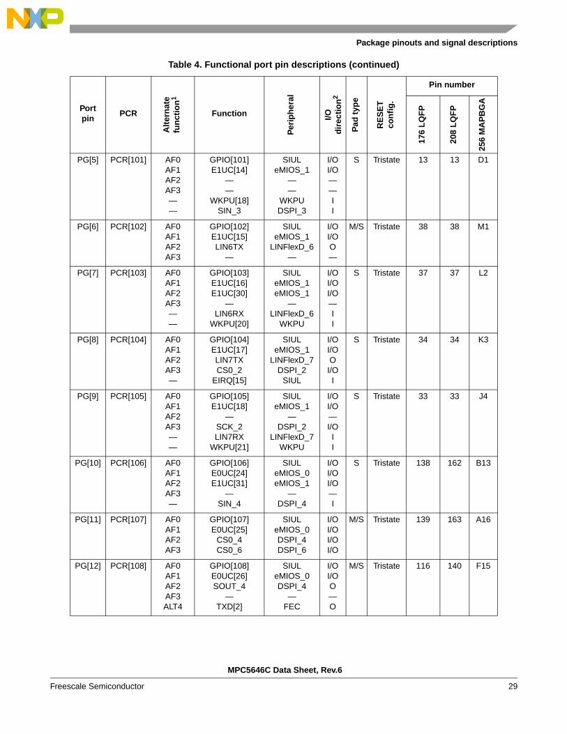
Table 4. Functional port pin descriptions
Portpin
PCR
Alt
ern
ate
fun
ctio
n1
Function
Per
iph
eral
I/Od
irec
tio
n2
Pad
typ
e
RE
SE
Tco
nfi
g.
Pin number
176
LQ
FP
208
LQ
FP
256
MA
PB
GA
PA[0] PCR[0] AF0AF1AF2AF3——
GPIO[0]E0UC[0]CLKOUTE0UC[13]WKPU[19]CAN1RX
SIULeMIOS_0MC_CGMeMIOS_0
WKPUFlexCAN_1
I/OI/OOI/OII
M/S Tristate 24 24 G4
PA[1] PCR[1] AF0AF1AF2AF3———
GPIO[1]E0UC[1]
——
WKPU[2]CAN3RXNMI[0]3
SIULeMIOS_0
——
WKPUFlexCAN_3
WKPU
I/OI/O——III
S Tristate 19 19 F3
PA[2] PCR[2] AF0AF1AF2AF3——
GPIO[2]E0UC[2]
—MA[2]
WKPU[3]NMI[1]3
SIULeMIOS_0
—ADC_0WKPUWKPU
I/OI/O—OII
S Tristate 17 17 F1
PA[3] PCR[3] AF0AF1AF2AF3———
GPIO[3]E0UC[3]LIN5TXCS4_1
RX_ER_CLKEIRQ[0]
ADC1_S[0]
SIULeMIOS_0
LINFlexD_5DSPI_1
FECSIUL
ADC_1
I/OI/OOOIII
M/S Tristate 114 138 G16
PA[4] PCR[4] AF0AF1AF2AF3——
GPIO[4]E0UC[4]
—CS0_1LIN5RX
WKPU[9]
SIULeMIOS_0
—DSPI_1
LINFlexD_5WKPU
I/OI/O—I/OII
S Tristate 51 61 T2
PA[5] PCR[5] AF0AF1AF2
GPIO[5]E0UC[5]LIN4TX
SIULeMIOS_0
LINFlexD_4
I/OI/OO
M/S Tristate 146 170 C10
PA[6] PCR[6] AF0AF1AF2AF3——
GPIO[6]E0UC[6]
—CS1_1LIN4RXEIRQ[1]
SIULeMIOS_0
—DSPI_1
LINFlexD_4SIUL
I/OI/O—OII
S Tristate 147 171 D11
MPC5646C Data Sheet, Rev.6
Freescale Semiconductor 15

Package pinouts and signal descriptions
PA[7] PCR[7] AF0AF1AF2AF3———
GPIO[7]E0UC[7]LIN3TX
—RXD[2]EIRQ[2]
ADC1_S[1]
SIULeMIOS_0
LINFlexD_3—
FECSIUL
ADC_1
I/OI/OO—III
M/S Tristate 128 152 C15
PA[8] PCR[8] AF0AF1AF2AF3————
GPIO[8]E0UC[8]
E0UC[14]—
RXD[1]EIRQ[3]ABS[0]LIN3RX
SIULeMIOS_0eMIOS_0
—FECSIUL
MC_RGMLINFlexD_3
I/OI/OI/O—IIII
M/S Input, weak
pull-up
129 153 B16
PA[9] PCR[9] AF0AF1AF2AF3——
GPIO[9]E0UC[9]
—CS2_1RXD[0]
FAB
SIULeMIOS_0
—DSPI1FEC
MC_RGM
I/OI/O—OII
M/S Pull-down
130 154 B15
PA[10] PCR[10] AF0AF1AF2AF3———
GPIO[10]E0UC[10]
SDALIN2TX
COLADC1_S[2]
SIN_1
SIULeMIOS_0
I2CLINFlexD_2
FECADC_1DSPI_1
I/OI/OI/OOIII
M/S Tristate 131 155 A15
PA[11] PCR[11] AF0AF1AF2AF3————
GPIO[11]E0UC[11]
SCL—
RX_EREIRQ[16]LIN2RX
ADC1_S[3]
SIULeMIOS_0
I2C—
FECSIUL
LINFlexD_2ADC_1
I/OI/OI/O—IIII
M/S Tristate 132 156 B14
PA[12] PCR[12] AF0AF1AF2AF3——
GPIO[12]—
E0UC[28]CS3_1
EIRQ[17]SIN_0
SIUL—
eMIOS_0DSPI1SIUL
DSPI_0
I/O—I/OOII
S Tristate 53 69 P6
Table 4. Functional port pin descriptions (continued)
Portpin
PCR
Alt
ern
ate
fun
ctio
n1
Function
Per
iph
eral
I/Od
irec
tio
n2
Pad
typ
e
RE
SE
Tco
nfi
g.
Pin number
176
LQ
FP
208
LQ
FP
256
MA
PB
GA
MPC5646C Data Sheet, Rev.6
Freescale Semiconductor16

Package pinouts and signal descriptions
PA[13] PCR[13] AF0AF1AF2AF3
GPIO[13]SOUT_0E0UC[29]
—
SIULDSPI_0
eMIOS_0—
I/OOI/O—
M/S Tristate 52 66 R5
PA[14] PCR[14] AF0AF1AF2AF3—
GPIO[14]SCK_0CS0_0
E0UC[0]EIRQ[4]
SIULDSPI_0DSPI_0
eMIOS_0SIUL
I/OI/OI/OI/OI
M/S Tristate 50 58 P4
PA[15] PCR[15] AF0AF1AF2AF3—
GPIO[15]CS0_0SCK_0
E0UC[1]WKPU[10]
SIULDSPI_0DSPI_0
eMIOS_0WKPU
I/OI/OI/OI/OI
M/S Tristate 48 56 R2
PB[0] PCR[16] AF0AF1AF2AF3
GPIO[16]CAN0TXE0UC[30]LIN0TX
SIULFlexCAN_0eMIOS_0
LINFlexD_0
I/OOI/OI
M/S Tristate 39 39 L3
PB[1] PCR[17] AF0AF1AF2———
GPIO[17]—
E0UC[31]LIN0RX
WKPU[4]CAN0RX
SIUL—
eMIOS_0LINFlexD_0
WKPUFlexCAN_0
I/O—I/OIII
S Tristate 40 40 M2
PB[2] PCR[18] AF0AF1AF2AF3
GPIO[18]LIN0TX
SDAE0UC[30]
SIULLINFlexD_0
I2CeMIOS_0
I/OOI/OI/O
M/S Tristate 176 208 A2
PB[3] PCR[19] AF0AF1AF2AF3——
GPIO[19]E0UC[31]
SCL—
WKPU[11]LIN0RX
SIULeMIOS_0
I2C—
WKPULINFlexD_0
I/OI/OI/O—II
S Tristate 1 1 D4
PB[4] PCR[20] AF0AF1AF2AF3——
GPI[20]———
ADC0_P[0]ADC1_P[0]
SIUL———
ADC_0ADC_1
I———II
I Tristate 88 104 T16
Table 4. Functional port pin descriptions (continued)
Portpin
PCR
Alt
ern
ate
fun
ctio
n1
Function
Per
iph
eral
I/Od
irec
tio
n2
Pad
typ
e
RE
SE
Tco
nfi
g.
Pin number
176
LQ
FP
208
LQ
FP
256
MA
PB
GA
MPC5646C Data Sheet, Rev.6
Freescale Semiconductor 17

Package pinouts and signal descriptions
PB[5] PCR[21] AF0AF1AF2AF3——
GPI[21]———
ADC0_P[1]ADC1_P[1]
SIUL———
ADC_0ADC_1
I———II
I Tristate 91 107 N13
PB[6] PCR[22] AF0AF1AF2AF3——
GPI[22]———
ADC0_P[2]ADC1_P[2]
SIUL———
ADC_0ADC_1
I———II
I Tristate 92 108 N14
PB[7] PCR[23] AF0AF1AF2AF3——
GPI[23]———
ADC0_P[3]ADC1_P[3]
SIUL———
ADC_0ADC_1
I———II
I Tristate 93 109 R16
PB[8] PCR[24] AF0AF1AF2AF3————
GPI[24]———
ADC0_S[0]ADC1_S[4]WKPU[25]
OSC32k_XTAL4
SIUL———
ADC_0ADC_1WKPUSXOSC
I———IIII
I — 61 77 T11
PB[9]5 PCR[25] AF0AF1AF2AF3————
GPI[25]———
ADC0_S[1]ADC1_S[5]WKPU[26]
OSC32k_EXTAL4
SIUL———
ADC_0ADC_1WKPUSXOSC
I———IIII
I — 60 76 T10
PB[10] PCR[26] AF0AF1AF2AF3———
GPIO[26]SOUT_1CAN3TX
—ADC0_S[2]ADC1_S[6]WKPU[8]
SIULDSPI_1
FlexCAN_3—
ADC_0ADC_1WKPU
I/OO——III
S Tristate 62 78 N7
Table 4. Functional port pin descriptions (continued)
Portpin
PCR
Alt
ern
ate
fun
ctio
n1
Function
Per
iph
eral
I/Od
irec
tio
n2
Pad
typ
e
RE
SE
Tco
nfi
g.
Pin number
176
LQ
FP
208
LQ
FP
256
MA
PB
GA
MPC5646C Data Sheet, Rev.6
Freescale Semiconductor18
Package pinouts and signal descriptions
PB[11] PCR[27] AF0AF1AF2AF3—
GPIO[27]E0UC[3]
—CS0_0
ADC0_S[3]
SIULeMIOS_0
—DSPI_0ADC_0
I/OI/O—I/OI
S Tristate 97 117 M13
PB[12] PCR[28] AF0AF1AF2AF3—
GPIO[28]E0UC[4]
—CS1_0
ADC0_X[0]
SIULeMIOS_0
—DSPI_0ADC_0
I/OI/O—OI
S Tristate 101 123 L14
PB[13] PCR[29] AF0AF1AF2AF3—
GPIO[29]E0UC[5]
—CS2_0
ADC0_X[1]
SIULeMIOS_0
—DSPI_0ADC_0
I/OI/O—OI
S Tristate 103 125 L15
PB[14] PCR[30] AF0AF1AF2AF3—
GPIO[30]E0UC[6]
—CS3_0
ADC0_X[2]
SIULeMIOS_0
—DSPI_0ADC_0
I/OI/O—OI
S Tristate 105 127 K15
PB[15] PCR[31] AF0AF1AF2AF3—
GPIO[31]E0UC[7]
—CS4_0
ADC0_X[3]
SIULeMIOS_0
—DSPI_0ADC_0
I/OI/O—OI
S Tristate 107 129 K16
PC[0]6 PCR[32] AF0AF1AF2AF3
GPIO[32]—
TDI—
SIUL—
JTAGC—
I/O—I
—
M/S Input, weak
pull-up
154 178 B10
PC[1]6 PCR[33] AF0AF1AF2AF3
GPIO[33]—
TDO—
SIUL—
JTAGC—
I/O—O—
F/M Tristate 149 173 D9
PC[2] PCR[34] AF0AF1AF2AF3—
GPIO[34]SCK_1
CAN4TX—
EIRQ[5]
SIULDSPI_1
FlexCAN_4—
SIUL
I/OI/OO—I
M/S Tristate 145 169 B11
Table 4. Functional port pin descriptions (continued)
Portpin
PCR
Alt
ern
ate
fun
ctio
n1
Function
Per
iph
eral
I/Od
irec
tio
n2
Pad
typ
e
RE
SE
Tco
nfi
g.
Pin number
176
LQ
FP
208
LQ
FP
256
MA
PB
GA
MPC5646C Data Sheet, Rev.6
Freescale Semiconductor 19

Package pinouts and signal descriptions
PC[3] PCR[35] AF0AF1AF2AF3———
GPIO[35]CS0_1MA[0]
—CAN1RXCAN4RXEIRQ[6]
SIULDSPI_1ADC_0
—FlexCAN_1FlexCAN_4
SIUL
I/OI/OO
III
S Tristate 144 168 C11
PC[4] PCR[36] AF0AF1AF2AF3ALT4
———
GPIO[36]E1UC[31]
—
FR_B_TX_ENSIN_1
CAN3RXEIRQ[18]
SIULeMIOS_1
—
FlexrayDSPI_1
FlexCAN_3SIUL
I/OI/O—
OIII
M/S Tristate 159 183 A9
PC[5] PCR[37] AF0AF1AF2AF3ALT4
—
GPIO[37]SOUT_1CAN3TX
—FR_A_TXEIRQ[7]
SIULDSPI_1
FlexCAN_3—
FlexraySIUL
I/OOO—OI
M/S Tristate 158 182 B9
PC[6] PCR[38] AF0AF1AF2AF3
GPIO[38]LIN1TX
E1UC[28]—
SIULLINFlexD_1eMIOS_1
—
I/OOI/O—
S Tristate 44 52 N3
PC[7] PCR[39] AF0AF1AF2AF3——
GPIO[39]—
E1UC[29]—
LIN1RXWKPU[12]
SIUL—
eMIOS_1—
LINFlexD_1WKPU
I/O—I/O—II
S Tristate 45 53 N4
PC[8] PCR[40] AF0AF1AF2AF3
GPIO[40]LIN2TXE0UC[3]
—
SIULLINFlexD_2eMIOS_0
—
I/OOI/O—
S Tristate 175 207 B3
PC[9] PCR[41] AF0AF1AF2AF3——
GPIO[41]—
E0UC[7]—
LIN2RXWKPU[13]
SIUL—
eMIOS_0—
LINFlexD_2WKPU
I/O—I/O—II
S Tristate 2 2 C3
Table 4. Functional port pin descriptions (continued)
Portpin
PCR
Alt
ern
ate
fun
ctio
n1
Function
Per
iph
eral
I/Od
irec
tio
n2
Pad
typ
e
RE
SE
Tco
nfi
g.
Pin number
176
LQ
FP
208
LQ
FP
256
MA
PB
GA
MPC5646C Data Sheet, Rev.6
Freescale Semiconductor20

Package pinouts and signal descriptions
PC[10] PCR[42] AF0AF1AF2AF3
GPIO[42]CAN1TXCAN4TX
MA[1]
SIULFlexCAN_1FlexCAN_4
ADC_0
I/OOOO
M/S Tristate 36 36 L1
PC[11] PCR[43] AF0AF1AF2AF3———
GPIO[43]——
MA[2]CAN1RXCAN4RXWKPU[5]
SIUL——
ADC_0FlexCAN_1FlexCAN_4
WKPU
I/O——OIII
S Tristate 35 35 K4
PC[12] PCR[44] AF0AF1AF2AF3ALT4
——
GPIO[44]E0UC[12]
——
FR_DBG[0]SIN_2
EIRQ[19]
SIULeMIOS_0
——
FlexrayDSPI_2
SIUL
I/OI/O——OII
M/S Tristate 173 205 B4
PC[13] PCR[45] AF0AF1AF2AF3ALT4
GPIO[45]E0UC[13]SOUT_2
—FR_DBG[1]
SIULeMIOS_0DSPI_2
—Flexray
I/OI/OO—O
M/S Tristate 174 206 A3
PC[14] PCR[46] AF0AF1AF2AF3ALT4
—
GPIO[46]E0UC[14]
SCK_2—
FR_DBG[2]EIRQ[8]
SIULeMIOS_0DSPI_2
—FlexraySIUL
I/OI/OI/O—OI
M/S Tristate 3 3 B2
PC[15] PCR[47] AF0AF1AF2AF3ALT4
GPIO[47]E0UC[15]
CS0_2—
FR_DBG[3]EIRQ[20]
SIULeMIOS_0DSPI_2
—FlexraySIUL
I/OI/OI/O—OI
M/S Tristate 4 4 A1
PD[0] PCR[48] AF0AF1AF2AF3———
GPI[48]———
ADC0_P[4]ADC1_P[4]WKPU[27]
SIUL———
ADC_0ADC_1WKPU
I———III
I Tristate 77 93 R12
Table 4. Functional port pin descriptions (continued)
Portpin
PCR
Alt
ern
ate
fun
ctio
n1
Function
Per
iph
eral
I/Od
irec
tio
n2
Pad
typ
e
RE
SE
Tco
nfi
g.
Pin number
176
LQ
FP
208
LQ
FP
256
MA
PB
GA
MPC5646C Data Sheet, Rev.6
Freescale Semiconductor 21
Package pinouts and signal descriptions
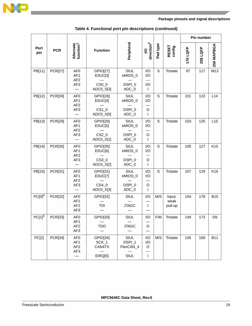
PD[1] PCR[49] AF0AF1AF2AF3———
GPI[49]———
ADC0_P[5]ADC1_P[5]WKPU[28]
SIUL———
ADC_0ADC_1WKPU
I———III
I Tristate 78 94 T13
PD[2] PCR[50] AF0AF1AF2AF3——
GPI[50]———
ADC0_P[6]ADC1_P[6]
SIUL———
ADC_0ADC_1
I———II
I Tristate 79 95 N11
PD[3] PCR[51] AF0AF1AF2AF3——
GPI[51]———
ADC0_P[7]ADC1_P[7]
SIUL———
ADC_0ADC_1
I———II
I Tristate 80 96 R13
PD[4] PCR[52] AF0AF1AF2AF3——
GPI[52]———
ADC0_P[8]ADC1_P[8]
SIUL———
ADC_0ADC_1
I———II
I Tristate 81 97 P12
PD[5] PCR[53] AF0AF1AF2AF3——
GPI[53]———
ADC0_P[9]ADC1_P[9]
SIUL———
ADC_0ADC_1
I———II
I Tristate 82 98 T14
PD[6] PCR[54] AF0AF1AF2AF3——
GPI[54]———
ADC0_P[10]ADC1_P[10]
SIUL———
ADC_0ADC_1
I———II
I Tristate 83 99 R14
PD[7] PCR[55] AF0AF1AF2AF3——
GPI[55]———
ADC0_P[11]ADC1_P[11]
SIUL———
ADC_0ADC_1
I———II
I Tristate 84 100 P13
Table 4. Functional port pin descriptions (continued)
Portpin
PCR
Alt
ern
ate
fun
ctio
n1
Function
Per
iph
eral
I/Od
irec
tio
n2
Pad
typ
e
RE
SE
Tco
nfi
g.
Pin number
176
LQ
FP
208
LQ
FP
256
MA
PB
GA
MPC5646C Data Sheet, Rev.6
Freescale Semiconductor22

Package pinouts and signal descriptions
PD[8] PCR[56] AF0AF1AF2AF3——
GPI[56]———
ADC0_P[12]ADC1_P[12]
SIUL———
ADC_0ADC_1
I———II
I Tristate 87 103 P14
PD[9] PCR[57] AF0AF1AF2AF3——
GPI[57]———
ADC0_P[13]ADC1_P[13]
SIUL———
ADC_0ADC_1
I———II
I Tristate 94 114 N16
PD[10] PCR[58] AF0AF1AF2AF3——
GPI[58]———
ADC0_P[14]ADC1_P[14]
SIUL———
ADC_0ADC_1
I———II
I Tristate 95 115 M14
PD[11] PCR[59] AF0AF1AF2AF3——
GPI[59]———
ADC0_P[15]ADC1_P[15]
SIUL———
ADC_0ADC_1
I———II
I Tristate 96 116 M15
PD[12] PCR[60] AF0AF1AF2AF3—
GPIO[60]CS5_0
E0UC[24]—
ADC0_S[4]
SIULDSPI_0
eMIOS_0—
ADC_0
I/OOI/O—I
S Tristate 100 120 L13
PD[13] PCR[61] AF0AF1AF2AF3—
GPIO[61]CS0_1
E0UC[25]—
ADC0_S[5]
SIULDSPI_1
eMIOS_0—
ADC_0
I/OI/OI/O—I
S Tristate 102 124 K14
PD[14] PCR[62] AF0AF1AF2AF3ALT4
—
GPIO[62]CS1_1
E0UC[26]—
FR_DBG[0]ADC0_S[6]
SIULDSPI_1
eMIOS_0—
FlexrayADC_0
I/OOI/O—OI
S Tristate 104 126 K13
Table 4. Functional port pin descriptions (continued)
Portpin
PCR
Alt
ern
ate
fun
ctio
n1
Function
Per
iph
eral
I/Od
irec
tio
n2
Pad
typ
e
RE
SE
Tco
nfi
g.
Pin number
176
LQ
FP
208
LQ
FP
256
MA
PB
GA
MPC5646C Data Sheet, Rev.6
Freescale Semiconductor 23

Package pinouts and signal descriptions
PD[15] PCR[63] AF0AF1AF2AF3ALT4
—
GPIO[63]CS2_1
E0UC[27]—
FR_DBG[1]ADC0_S[7]
SIULDSPI_1
eMIOS_0—
FlexrayADC_0
I/OOI/O—OI
S Tristate 106 128 J13
PE[0] PCR[64] AF0AF1AF2AF3——
GPIO[64]E0UC[16]
——
CAN5RXWKPU[6]
SIULeMIOS_0
——
FlexCAN_5WKPU
I/OI/O——II
S Tristate 18 18 G2
PE[1] PCR[65] AF0AF1AF2AF3
GPIO[65]E0UC[17]CAN5TX
—
SIULeMIOS_0
FlexCAN_5—
I/OI/OO—
M/S Tristate 20 20 F4
PE[2] PCR[66] AF0AF1AF2AF3ALT4
——
GPIO[66]E0UC[18]
——
FR_A_TX_ENSIN_1
EIRQ[21]
SIULeMIOS_0
——
FlexrayDSPI_1
SIUL
I/OI/O——OII
M/S Tristate 156 180 A7
PE[3] PCR[67] AF0AF1AF2AF3——
GPIO[67]E0UC[19]SOUT_1
—FR_A_RXWKPU[29]
SIULeMIOS_0DSPI_1
—FlexrayWKPU
I/OI/OO—II
M/S Tristate 157 181 A10
PE[4] PCR[68] AF0AF1AF2AF3ALT4
—
GPIO[68]E0UC[20]
SCK_1—
FR_B_TXEIRQ[9]
SIULeMIOS_0DSPI_1
—FlexraySIUL
I/OI/OI/O—OI
M/S Tristate 160 184 A8
PE[5] PCR[69] AF0AF1AF2AF3——
GPIO[69]E0UC[21]
CS0_1MA[2]
FR_B_RXWKPU[30]
SIULeMIOS_0DSPI_1ADC_0FlexrayWKPU
I/OI/OI/OOII
M/S Tristate 161 185 B8
Table 4. Functional port pin descriptions (continued)
Portpin
PCR
Alt
ern
ate
fun
ctio
n1
Function
Per
iph
eral
I/Od
irec
tio
n2
Pad
typ
e
RE
SE
Tco
nfi
g.
Pin number
176
LQ
FP
208
LQ
FP
256
MA
PB
GA
MPC5646C Data Sheet, Rev.6
Freescale Semiconductor24

Package pinouts and signal descriptions
PE[6] PCR[70] AF0AF1AF2AF3—
GPIO[70]E0UC[22]
CS3_0MA[1]
EIRQ[22]
SIULeMIOS_0DSPI_0ADC_0SIUL
I/OI/OOOI
M/S Tristate 167 191 B6
PE[7] PCR[71] AF0AF1AF2AF3—
GPIO[71]E0UC[23]
CS2_0MA[0]
EIRQ[23]
SIULeMIOS_0DSPI_0ADC_0SIUL
I/OI/OOOI
M/S Tristate 168 192 A5
PE[8] PCR[72] AF0AF1AF2AF3
GPIO[72]CAN2TXE0UC[22]CAN3TX
SIULFlexCAN_2eMIOS_0
FlexCAN_3
I/OOI/OO
M/S Tristate 21 21 G1
PE[9] PCR[73] AF0AF1AF2AF3———
GPIO[73]—
E0UC[23]—
WKPU[7]CAN2RXCAN3RX
SIUL—
eMIOS_0—
WKPUFlexCAN_2FlexCAN_3
I/O—I/O—III
S Tristate 22 22 H1
PE[10] PCR[74] AF0AF1AF2AF3—
GPIO[74]LIN3TXCS3_1
E1UC[30]EIRQ[10]
SIULLINFlexD_3
DSPI_1eMIOS_1
SIUL
I/OOOI/OI
S Tristate 23 23 G3
PE[11] PCR[75] AF0AF1AF2AF3——
GPIO[75]E0UC[24]
CS4_1—
LIN3RXWKPU[14]
SIULeMIOS_0DSPI_1
—LINFlexD_3
WKPU
I/OI/OO—II
S Tristate 25 25 H3
PE[12] PCR[76] AF0AF1AF2AF3————
GPIO[76]—
E1UC[19]—
CRSSIN_2
EIRQ[11]ADC1_S[7]
SIUL—
eMIOS_1—
FECDSPI_2
SIULADC_1
I/O—I/O—IIII
M/S Tristate 133 157 C14
Table 4. Functional port pin descriptions (continued)
Portpin
PCR
Alt
ern
ate
fun
ctio
n1
Function
Per
iph
eral
I/Od
irec
tio
n2
Pad
typ
e
RE
SE
Tco
nfi
g.
Pin number
176
LQ
FP
208
LQ
FP
256
MA
PB
GA
MPC5646C Data Sheet, Rev.6
Freescale Semiconductor 25
Package pinouts and signal descriptions
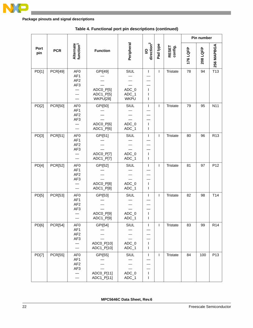
PE[13] PCR[77] AF0AF1AF2AF3—
GPIO[77]SOUT_2E1UC[20]
—RXD[3]
SIULDSPI_2
eMIOS_1—
FEC
I/OOI/O—I
M/S Tristate 127 151 C16
PE[14] PCR[78] AF0AF1AF2AF3—
GPIO[78]SCK_2
E1UC[21]—
EIRQ[12]
SIULDSPI_2
eMIOS_1—
SIUL
I/OI/OI/O—I
M/S Tristate 136 160 A14
PE[15] PCR[79] AF0AF1AF2AF3
GPIO[79]CS0_2
E1UC[22]SCK_6
SIULDSPI_2
eMIOS_1DSPI_6
I/OI/OI/OI/O
M/S Tristate 137 161 C12
PF[0] PCR[80] AF0AF1AF2AF3—
GPIO[80]E0UC[10]
CS3_1—
ADC0_S[8]
SIULeMIOS_0DSPI_1
—ADC_0
I/OI/OO—I
S Tristate 63 79 P7
PF[1] PCR[81] AF0AF1AF2AF3—
GPIO[81]E0UC[11]
CS4_1—
ADC0_S[9]
SIULeMIOS_0DSPI_1
—ADC_0
I/OI/OO—I
S Tristate 64 80 T6
PF[2] PCR[82] AF0AF1AF2AF3—
GPIO[82]E0UC[12]
CS0_2—
ADC0_S[10]
SIULeMIOS_0DSPI_2
—ADC_0
I/OI/OI/O—I
S Tristate 65 81 R6
PF[3] PCR[83] AF0AF1AF2AF3—
GPIO[83]E0UC[13]
CS1_2—
ADC0_S[11]
SIULeMIOS_0DSPI_2
—ADC_0
I/OI/OO—I
S Tristate 66 82 R7
PF[4] PCR[84] AF0AF1AF2AF3—
GPIO[84]E0UC[14]
CS2_2—
ADC0_S[12]
SIULeMIOS_0DSPI_2
—ADC_0
I/OI/OO—I
S Tristate 67 83 R8
Table 4. Functional port pin descriptions (continued)
Portpin
PCR
Alt
ern
ate
fun
ctio
n1
Function
Per
iph
eral
I/Od
irec
tio
n2
Pad
typ
e
RE
SE
Tco
nfi
g.
Pin number
176
LQ
FP
208
LQ
FP
256
MA
PB
GA
MPC5646C Data Sheet, Rev.6
Freescale Semiconductor26

Package pinouts and signal descriptions
PF[5] PCR[85] AF0AF1AF2AF3—
GPIO[85]E0UC[22]
CS3_2—
ADC0_S[13]
SIULeMIOS_0DSPI_2
—ADC_0
I/OI/OO—I
S Tristate 68 84 P8
PF[6] PCR[86] AF0AF1AF2AF3—
GPIO[86]E0UC[23]
CS1_1—
ADC0_S[14]
SIULeMIOS_0DSPI_1
—ADC_0
I/OI/OO—I
S Tristate 69 85 N8
PF[7] PCR[87] AF0AF1AF2AF3—
GPIO[87]—
CS2_1—
ADC0_S[15]
SIUL—
DSPI_1—
ADC_0
I/O—O—I
S Tristate 70 86 P9
PF[8] PCR[88] AF0AF1AF2AF3
GPIO[88]CAN3TXCS4_0
CAN2TX
SIULFlexCAN_3
DSPI_0FlexCAN_2
I/OOOO
M/S Tristate 42 50 N2
PF[9] PCR[89] AF0AF1AF2AF3———
GPIO[89]E1UC[1]CS5_0
—CAN2RXCAN3RX
WKPU[22]
SIULeMIOS_1DSPI_0
—FlexCAN_2FlexCAN_3
WKPU
I/OI/OO—III
S Tristate 41 49 M4
PF[10] PCR[90] AF0AF1AF2AF3
GPIO[90]CS1_0LIN4TXE1UC[2]
SIULDSPI_0
LINFlexD_4eMIOS_1
I/OOOI/O
M/S Tristate 46 54 P2
PF[11] PCR[91] AF0AF1AF2AF3——
GPIO[91]CS2_0
E1UC[3]—
LIN4RXWKPU[15]
SIULDSPI_0
eMIOS_1—
LINFlexD_4WKPU
I/OOI/O—II
S Tristate 47 55 R1
PF[12] PCR[92] AF0AF1AF2AF3
GPIO[92]E1UC[25]LIN5TX
—
SIULeMIOS_1
LINFlexD_5—
I/OI/OO—
M/S Tristate 43 51 P1
Table 4. Functional port pin descriptions (continued)
Portpin
PCR
Alt
ern
ate
fun
ctio
n1
Function
Per
iph
eral
I/Od
irec
tio
n2
Pad
typ
e
RE
SE
Tco
nfi
g.
Pin number
176
LQ
FP
208
LQ
FP
256
MA
PB
GA
MPC5646C Data Sheet, Rev.6
Freescale Semiconductor 27

Package pinouts and signal descriptions
PF[13] PCR[93] AF0AF1AF2AF3——
GPIO[93]E1UC[26]
——
LIN5RXWKPU[16]
SIULeMIOS_1
——
LINFlexD_5WKPU
I/OI/O——II
S Tristate 49 57 P3
PF[14] PCR[94] AF0AF1AF2AF3ALT4
GPIO[94]CAN4TXE1UC[27]CAN1TX
MDIO
SIULFlexCAN_4eMIOS_1
FlexCAN_1FEC
I/OOI/OOI/O
M/S Tristate 126 150 D14
PF[15] PCR[95] AF0AF1AF2AF3————
GPIO[95]E1UC[4]
——
RX_DVCAN1RXCAN4RXEIRQ[13]
SIULeMIOS_1
——
FECFlexCAN_1FlexCAN_4
SIUL
I/OI/O——IIII
M/S Tristate 125 149 D15
PG[0] PCR[96] AF0AF1AF2AF3ALT4
GPIO[96]CAN5TXE1UC[23]
—MDC
SIULFlexCAN_5eMIOS_1
—FEC
I/OOI/O—O
F Tristate 122 146 E13
PG[1] PCR[97] AF0AF1AF2AF3———
GPIO[97]—
E1UC[24]—
TX_CLKCAN5RXEIRQ[14]
SIUL—
eMIOS_1—
FECFlexCAN_5
SIUL
I/O—I/O—III
M Tristate 121 145 E14
PG[2] PCR[98] AF0AF1AF2AF3
GPIO[98]E1UC[11]SOUT_3
—
SIULeMIOS_1DSPI_3
—
I/OI/OO—
M/S Tristate 16 16 E4
PG[3] PCR[99] AF0AF1AF2AF3—
GPIO[99]E1UC[12]
CS0_3—
WKPU[17]
SIULeMIOS_1DSPI_3
—WKPU
I/OI/OI/O—I
S Tristate 15 15 E1
PG[4] PCR[100] AF0AF1AF2AF3
GPIO[100]E1UC[13]
SCK_3—
SIULeMIOS_1DSPI_3
—
I/OI/OI/O—
M/S Tristate 14 14 F2
Table 4. Functional port pin descriptions (continued)
Portpin
PCR
Alt
ern
ate
fun
ctio
n1
Function
Per
iph
eral
I/Od
irec
tio
n2
Pad
typ
e
RE
SE
Tco
nfi
g.
Pin number
176
LQ
FP
208
LQ
FP
256
MA
PB
GA
MPC5646C Data Sheet, Rev.6
Freescale Semiconductor28
Package pinouts and signal descriptions
PG[5] PCR[101] AF0AF1AF2AF3——
GPIO[101]E1UC[14]
——
WKPU[18]SIN_3
SIULeMIOS_1
——
WKPUDSPI_3
I/OI/O——II
S Tristate 13 13 D1
PG[6] PCR[102] AF0AF1AF2AF3
GPIO[102]E1UC[15]LIN6TX
—
SIULeMIOS_1
LINFlexD_6—
I/OI/OO—
M/S Tristate 38 38 M1
PG[7] PCR[103] AF0AF1AF2AF3——
GPIO[103]E1UC[16]E1UC[30]
—LIN6RX
WKPU[20]
SIULeMIOS_1eMIOS_1
—LINFlexD_6
WKPU
I/OI/OI/O—II
S Tristate 37 37 L2
PG[8] PCR[104] AF0AF1AF2AF3—
GPIO[104]E1UC[17]LIN7TXCS0_2
EIRQ[15]
SIULeMIOS_1
LINFlexD_7DSPI_2
SIUL
I/OI/OOI/OI
S Tristate 34 34 K3
PG[9] PCR[105] AF0AF1AF2AF3——
GPIO[105]E1UC[18]
—SCK_2LIN7RX
WKPU[21]
SIULeMIOS_1
—DSPI_2
LINFlexD_7WKPU
I/OI/O—I/OII
S Tristate 33 33 J4
PG[10] PCR[106] AF0AF1AF2AF3—
GPIO[106]E0UC[24]E1UC[31]
—SIN_4
SIULeMIOS_0eMIOS_1
—DSPI_4
I/OI/OI/O—I
S Tristate 138 162 B13
PG[11] PCR[107] AF0AF1AF2AF3
GPIO[107]E0UC[25]
CS0_4CS0_6
SIULeMIOS_0DSPI_4DSPI_6
I/OI/OI/OI/O
M/S Tristate 139 163 A16
PG[12] PCR[108] AF0AF1AF2AF3ALT4
GPIO[108]E0UC[26]SOUT_4
—TXD[2]
SIULeMIOS_0DSPI_4
—FEC
I/OI/OO—O
M/S Tristate 116 140 F15
Table 4. Functional port pin descriptions (continued)
Portpin
PCR
Alt
ern
ate
fun
ctio
n1
Function
Per
iph
eral
I/Od
irec
tio
n2
Pad
typ
e
RE
SE
Tco
nfi
g.
Pin number
176
LQ
FP
208
LQ
FP
256
MA
PB
GA
MPC5646C Data Sheet, Rev.6
Freescale Semiconductor 29

Package pinouts and signal descriptions
PG[13] PCR[109] AF0AF1AF2AF3ALT4
GPIO[109]E0UC[27]
SCK_4—
TXD[3]
SIULeMIOS_0DSPI_4
—FEC
I/OI/OI/O—O
M/S Tristate 115 139 F16
PG[14] PCR[110] AF0AF1AF2AF3—
GPIO[110]E1UC[0]LIN8TX
—SIN_6
SIULeMIOS_1
LINFlexD_8—
DSPI_6
I/OI/OO—I
S Tristate 134 158 C13
PG[15] PCR[111] AF0AF1AF2AF3—
GPIO[111]E1UC[1]SOUT_6
—LIN8RX
SIULeMIOS_1DSPI_6
—LINFlexD_8
I/OI/OO—I
M/S Tristate 135 159 D13
PH[0] PCR[112] AF0AF1AF2AF3ALT4
—
GPIO[112]E1UC[2]
——
TXD[1]SIN_1
SIULeMIOS_1
——
FECDSPI_1
I/OI/O——OI
M/S Tristate 117 141 E15
PH[1] PCR[113] AF0AF1AF2AF3ALT4
GPIO[113]E1UC[3]SOUT_1
—TXD[0]
SIULeMIOS_1DSPI_1
—FEC
I/OI/OO—O
M/S Tristate 118 142 F13
PH[2] PCR[114] AF0AF1AF2AF3ALT4
GPIO[114]E1UC[4]SCK_1
—TX_EN
SIULeMIOS_1DSPI_1
—FEC
I/OI/OI/O—O
M/S Tristate 119 143 D16
PH[3] PCR[115] AF0AF1AF2AF3ALT4
GPIO[115]E1UC[5]CS0_1
—TX_ER
SIULeMIOS_1DSPI_1
—FEC
I/OI/OI/O—O
M/S Tristate 120 144 F14
PH[4] PCR[116] AF0AF1AF2AF3
GPIO[116]E1UC[6]SOUT_7
—
SIULeMIOS_1DSPI_7
—
I/OI/OO—
M/S Tristate 162 186 D7
Table 4. Functional port pin descriptions (continued)
Portpin
PCR
Alt
ern
ate
fun
ctio
n1
Function
Per
iph
eral
I/Od
irec
tio
n2
Pad
typ
e
RE
SE
Tco
nfi
g.
Pin number
176
LQ
FP
208
LQ
FP
256
MA
PB
GA
MPC5646C Data Sheet, Rev.6
Freescale Semiconductor30

Package pinouts and signal descriptions
PH[5] PCR[117] AF0AF1AF2AF3—
GPIO[117]E1UC[7]
——
SIN_7
SIULeMIOS_1
——
DSPI_7
I/OI/O——I
S Tristate 163 187 B7
PH[6] PCR[118] AF0AF1AF2AF3
GPIO[118]E1UC[8]SCK_7MA[2]
SIULeMIOS_1DSPI_7ADC_0
I/OI/OI/OO
M/S Tristate 164 188 C7
PH[7] PCR[119] AF0AF1AF2AF3ALT4
GPIO[119]E1UC[9]CS3_2MA[1]CS0_7
SIULeMIOS_1DSPI_2ADC_0DSPI_7
I/OI/OOOI/O
M/S Tristate 165 189 C6
PH[8] PCR[120] AF0AF1AF2AF3
GPIO[120]E1UC[10]
CS2_2MA[0]
SIULeMIOS_1DSPI_2ADC_0
I/OI/OOO
M/S Tristate 166 190 A6
PH[9]6 PCR[121] AF0AF1AF2AF3—
GPIO[121]———
TCK
SIUL———
JTAGC
I/O———I
S Input, weak
pull-up
155 179 A11
PH[10]6 PCR[122] AF0AF1AF2AF3—
GPIO[122]———
TMS
SIUL———
JTAGC
I/O———I
M/S Input, weak
pull-up
148 172 D10
PH[11] PCR[123] AF0AF1AF2AF3
GPIO[123]SOUT_3CS0_4
E1UC[5]
SIULDSPI_3DSPI_4
eMIOS_1
I/OOI/OI/O
M/S Tristate 140 164 A13
PH[12] PCR[124] AF0AF1AF2AF3
GPIO[124]SCK_3CS1_4
E1UC[25]
SIULDSPI_3DSPI_4
eMIOS_1
I/OI/OOI/O
M/S Tristate 141 165 B12
PH[13] PCR[125] AF0AF1AF2AF3
GPIO[125]SOUT_4CS0_3
E1UC[26]
SIULDSPI_4DSPI_3
eMIOS_1
I/OOI/OI/O
M/S Tristate 9 9 B1
Table 4. Functional port pin descriptions (continued)
Portpin
PCR
Alt
ern
ate
fun
ctio
n1
Function
Per
iph
eral
I/Od
irec
tio
n2
Pad
typ
e
RE
SE
Tco
nfi
g.
Pin number
176
LQ
FP
208
LQ
FP
256
MA
PB
GA
MPC5646C Data Sheet, Rev.6
Freescale Semiconductor 31

Package pinouts and signal descriptions
PH[14] PCR[126] AF0AF1AF2AF3
GPIO[126]SCK_4CS1_3
E1UC[27]
SIULDSPI_4DSPI_3
eMIOS_1
I/OI/OOI/O
M/S Tristate 10 10 C1
PH[15] PCR[127] AF0AF1AF2AF3
GPIO[127]SOUT_5
—E1UC[17]
SIULDSPI_5
—eMIOS_1
I/OO—I/O
M/S Tristate 8 8 E3
PI[0] PCR[128] AF0AF1AF2AF3
GPIO[128]E0UC[28]LIN8TX
—
SIULeMIOS_0
LINFlexD_8—
I/OI/OO—
S Tristate 172 196 C5
PI[1] PCR[129] AF0AF1AF2AF3——
GPIO[129]E0UC[29]
——
WKPU[24]LIN8RX
SIULeMIOS_0
——
WKPULINFlexD_8
I/OI/O——II
S Tristate 171 195 A4
PI[2] PCR[130] AF0AF1AF2AF3
GPIO[130]E0UC[30]LIN9TX
—
SIULeMIOS_0
LINFlexD_9—
I/OI/OO—
S Tristate 170 194 D6
PI[3] PCR[131] AF0AF1AF2AF3——
GPIO[131]E0UC[31]
——
WKPU[23]LIN9RX
SIULeMIOS_0
——
WKPULINFlexD_9
I/OI/O——II
S Tristate 169 193 B5
PI[4] PCR[132] AF0AF1AF2AF3
GPIO[132]E1UC[28]SOUT_4
—
SIULeMIOS_1DSPI_4
—
I/OI/OO—
M/S Tristate 143 167 A12
PI[5] PCR[133] AF0AF1AF2AF3ALT4
GPIO[133]E1UC[29]
SCK_4CS2_5CS2_6
SIULeMIOS_1DSPI_4DSPI_5DSPI_6
I/OI/OI/OOO
M/S Tristate 142 166 D12
PI[6] PCR[134] AF0AF1AF2AF3ALT4
GPIO[134]E1UC[30]
CS0_4CS0_5CS0_6
SIULeMIOS_1DSPI_4DSPI_5DSPI_6
I/OI/OI/OI/OI/O
S Tristate 11 11 D2
Table 4. Functional port pin descriptions (continued)
Portpin
PCR
Alt
ern
ate
fun
ctio
n1
Function
Per
iph
eral
I/Od
irec
tio
n2
Pad
typ
e
RE
SE
Tco
nfi
g.
Pin number
176
LQ
FP
208
LQ
FP
256
MA
PB
GA
MPC5646C Data Sheet, Rev.6
Freescale Semiconductor32

Package pinouts and signal descriptions
PI[7] PCR[135] AF0AF1AF2AF3ALT4
GPIO[135]E1UC[31]
CS1_4CS1_5CS1_6
SIULeMIOS_1DSPI_4DSPI_5DSPI_6
I/OI/OOOO
S Tristate 12 12 E2
PI[8] PCR[136] AF0AF1AF2AF3—
GPIO[136]———
ADC0_S[16]
SIUL———
ADC_0
I/O———I
S Tristate 108 130 J14
PI[9] PCR[137] AF0AF1AF2AF3—
GPIO[137]———
ADC0_S[17]
SIUL———
ADC_0
I/O———I
S Tristate — 131 J15
PI[10] PCR[138] AF0AF1AF2AF3—
GPIO[138]———
ADC0_S[18]
SIUL———
ADC_0
I/O———I
S Tristate — 134 J16
PI[11] PCR[139] AF0AF1AF2AF3——
GPIO[139]———
ADC0_S[19]SIN_3
SIUL———
ADC_0DSPI_3
I/O———II
S Tristate 111 135 H16
PI[12] PCR[140] AF0AF1AF2AF3—
GPIO[140]CS0_3CS0_2
—ADC0_S[20]
SIULDSPI_3DSPI_2
—ADC_0
I/OI/OI/O—I
S Tristate 112 136 G15
PI[13] PCR[141] AF0AF1AF2AF3—
GPIO[141]CS1_3CS1_2
—ADC0_S[21]
SIULDSPI_3DSPI_2
—ADC_0
I/OOO—I
S Tristate 113 137 G14
PI[14] PCR[142] AF0AF1AF2AF3——
GPIO[142]———
ADC0_S[22]SIN_4
SIUL———
ADC_0DSPI_4
I/O———II
S Tristate 76 92 T12
Table 4. Functional port pin descriptions (continued)
Portpin
PCR
Alt
ern
ate
fun
ctio
n1
Function
Per
iph
eral
I/Od
irec
tio
n2
Pad
typ
e
RE
SE
Tco
nfi
g.
Pin number
176
LQ
FP
208
LQ
FP
256
MA
PB
GA
MPC5646C Data Sheet, Rev.6
Freescale Semiconductor 33

Package pinouts and signal descriptions
PI[15] PCR[143] AF0AF1AF2AF3—
GPIO[143]CS0_4CS2_2
—ADC0_S[23]
SIULDSPI_4DSPI_2
—ADC_0
I/OI/OO—I
S Tristate 75 91 P11
PJ[0] PCR[144] AF0AF1AF2AF3—
GPIO[144]CS1_4CS3_2
—ADC0_S[24]
SIULDSPI_4DSPI_2
—ADC_0
I/OOO—I
S Tristate 74 90 R11
PJ[1] PCR[145] AF0AF1AF2AF3——
GPIO[145]———
ADC0_S[25]SIN_5
SIUL——
——ADC_0DSPI_5
I/O———II
S Tristate 73 89 N10
PJ[2] PCR[146] AF0AF1AF2AF3—
GPIO[146]CS0_5CS0_6CS0_7
ADC0_S[26]
SIULDSPI_5DSPI_6DSPI_7ADC_0
I/OI/OI/OI/OI
S Tristate 72 88 R10
PJ[3] PCR[147] AF0AF1AF2AF3—
GPIO[147]CS1_5CS1_6CS1_7
ADC0_S[27]
SIULDSPI_5DSPI_6DSPI_7ADC_0
I/OOOOI
S Tristate 71 87 P10
PJ[4] PCR[148] AF0AF1AF2AF3
GPIO[148]SCK_5
E1UC[18]—
SIULDSPI_5
eMIOS_1—
I/OI/OI/O—
M/S Tristate 5 5 D3
PJ[5] PCR[149] AF0AF1AF2AF3—
GPIO[149]———
ADC0_S[28]
SIUL———
ADC_0
I/O———I
S Tristate — 113 N12
PJ[6] PCR[150] AF0AF1AF2AF3—
GPIO[150]———
ADC0_S[29]
SIUL———
ADC_0
I/O———I
S Tristate — 112 N15
Table 4. Functional port pin descriptions (continued)
Portpin
PCR
Alt
ern
ate
fun
ctio
n1
Function
Per
iph
eral
I/Od
irec
tio
n2
Pad
typ
e
RE
SE
Tco
nfi
g.
Pin number
176
LQ
FP
208
LQ
FP
256
MA
PB
GA
MPC5646C Data Sheet, Rev.6
Freescale Semiconductor34

Package pinouts and signal descriptions
PJ[7] PCR[151] AF0AF1AF2AF3—
GPIO[151]———
ADC0_S[30]
SIUL———
ADC_0
I/O———I
S Tristate — 111 P16
PJ[8] PCR[152] AF0AF1AF2AF3—
GPIO[152]———
ADC0_S[31]
SIUL———
ADC_0
I/O———I
S Tristate — 110 P15
PJ[9] PCR[153] AF0AF1AF2AF3—
GPIO[153]———
ADC1_S[8]
SIUL———
ADC_1
I/O———I
S Tristate — 68 P5
PJ[10] PCR[154] AF0AF1AF2AF3—
GPIO[154]———
ADC1_S[9]
SIUL———
ADC_1
I/O———I
S Tristate — 67 T5
PJ[11] PCR[155] AF0AF1AF2AF3—
GPIO[155]———
ADC1_S[10]
SIUL———
ADC_1
I/O———I
S Tristate — 60 R3
PJ[12] PCR[156] AF0AF1AF2AF3—
GPIO[156]———
ADC1_S[11]
SIUL———
ADC_1
I/O———I
S Tristate — 59 T1
PJ[13] PCR[157] AF0AF1AF2AF3————
GPIO[157]—
CS1_7—
CAN4RXADC1_S[12]
CAN1RXWKPU[31]
SIUL—
DSPI_7—
FlexCAN_4ADC_1
FlexCAN_1WKPU
I/O—O—IIII
S Tristate — 65 N5
PJ[14] PCR[158] AF0AF1AF2AF3
GPIO[158]CAN1TXCAN4TXCS2_7
SIULFlexCAN_1FlexCAN_4
DSPI_7
I/OOOO
M/S Tristate — 64 T4
Table 4. Functional port pin descriptions (continued)
Portpin
PCR
Alt
ern
ate
fun
ctio
n1
Function
Per
iph
eral
I/Od
irec
tio
n2
Pad
typ
e
RE
SE
Tco
nfi
g.
Pin number
176
LQ
FP
208
LQ
FP
256
MA
PB
GA
MPC5646C Data Sheet, Rev.6
Freescale Semiconductor 35

Package pinouts and signal descriptions
PJ[15] PCR[159] AF0AF1AF2AF3—
GPIO[159]—
CS1_6—
CAN1RX
SIUL—
DSPI_6—
FlexCAN_1
I/O—O—I
M/S Tristate — 63 R4
PK[0] PCR[160] AF0AF1AF2AF3
GPIO[160]CAN1TXCS2_6
—
SIULFlexCAN_1
DSPI_6—
I/OOO—
M/S Tristate — 62 T3
PK[1] PCR[161] AF0AF1AF2AF3—
GPIO[161]CS3_6
——
CAN4RX
SIULDSPI_6
——
FlexCAN_4
I/OO——I
M/S Tristate — 41 H4
PK[2] PCR[162] AF0AF1AF2AF3
GPIO[162]CAN4TX
——
SIULFlexCAN_4
——
I/OO——
M/S Tristate — 42 L4
PK[3] PCR[163] AF0AF1AF2AF3——
GPIO[163]E1UC[0]
——
CAN5RXLIN8RX
SIULeMIOS_1
——
FlexCAN_5LINFlexD_8
I/OI/O——II
M/S Tristate — 43 N1
PK[4] PCR[164] AF0AF1AF2AF3
GPIO[164]LIN8TXCAN5TXE1UC[1]
SIULLINFlexD_8FlexCAN_5eMIOS_1
I/OOOI/O
M/S Tristate — 44 M3
PK[5] PCR[165] AF0AF1AF2AF3——
GPIO[165]———
CAN2RXLIN2RX
SIUL———
FlexCAN_2LINFlexD_2
I/O———II
M/S Tristate — 45 M5
PK[6] PCR[166] AF0AF1AF2AF3
GPIO[166]CAN2TXLIN2TX
—
SIULFlexCAN_2LINFlexD_2
—
I/OOO—
M/S Tristate — 46 M6
Table 4. Functional port pin descriptions (continued)
Portpin
PCR
Alt
ern
ate
fun
ctio
n1
Function
Per
iph
eral
I/Od
irec
tio
n2
Pad
typ
e
RE
SE
Tco
nfi
g.
Pin number
176
LQ
FP
208
LQ
FP
256
MA
PB
GA
MPC5646C Data Sheet, Rev.6
Freescale Semiconductor36

Package pinouts and signal descriptions
PK[7] PCR[167] AF0AF1AF2AF3——
GPIO[167]———
CAN3RXLIN3RX
SIUL———
FlexCAN_3LINFlexD_3
I/O———II
M/S Tristate — 47 M7
PK[8] PCR[168] AF0AF1AF2AF3
GPIO[168]CAN3TXLIN3TX
—
SIULFlexCAN_3LINFlexD_3
—
I/OOO—
M/S Tristate — 48 M8
PK[9] PCR[169] AF0AF1AF2AF3—
GPIO[169]———
SIN_4
SIUL———
DSPI_4
I/O———I
M/S Tristate — 197 E8
PK[10] PCR[170] AF0AF1AF2AF3
GPIO[170]SOUT_4
——
SIULDSPI_4
——
I/OO——
M/S Tristate — 198 E7
PK[11] PCR[171] AF0AF1AF2AF3
GPIO[171]SCK_4
——
SIULDSPI_4
——
I/OI/O——
M/S Tristate — 199 F8
PK[12] PCR[172] AF0AF1AF2AF3
GPIO[172]CS0_4
——
SIULDSPI_4
——
I/OI/O——
M/S Tristate — 200 G12
PK[13] PCR[173] AF0AF1AF2AF3—
GPIO[173]CS3_6CS2_7SCK_1
CAN3RX
SIULDSPI_6DSPI_7DSPI_1
FlexCAN_3
I/OOOI/OI
M/S Tristate — 201 H12
PK[14] PCR[174] AF0AF1AF2AF3
GPIO[174]CAN3TXCS3_7CS0_1
SIULFlexCAN_3
DSPI_7DSPI_1
I/OOOI/O
M/S Tristate — 202 J12
PK[15] PCR[175] AF0AF1AF2AF3——
GPIO[175]———
SIN_1SIN_7
SIUL———
DSPI_1DSPI_7
I/O———II
M/S Tristate — 203 D5
Table 4. Functional port pin descriptions (continued)
Portpin
PCR
Alt
ern
ate
fun
ctio
n1
Function
Per
iph
eral
I/Od
irec
tio
n2
Pad
typ
e
RE
SE
Tco
nfi
g.
Pin number
176
LQ
FP
208
LQ
FP
256
MA
PB
GA
MPC5646C Data Sheet, Rev.6
Freescale Semiconductor 37

Package pinouts and signal descriptions
PL[0] PCR[176] AF0AF1AF2AF3
GPIO[176]SOUT_1SOUT_7
—
SIULDSPI_1DSPI_7
—
I/OOO—
M/S Tristate — 204 C4
PL[1] PCR[177] AF0AF1AF2AF3
GPIO[177]———
SIUL———
I/O———
M/S Tristate — — F7
PL[2] PCR[178]7 AF0AF1AF2AF3
GPIO[178]—
MDO08
—
SIUL—
Nexus—
I/O—O—
M/S Tristate — — F5
PL[3] PCR[179] AF0AF1AF2AF3
GPIO[179]—
MDO1—
SIUL—
Nexus—
I/O—O—
M/S Tristate — — G5
PL[4] PCR[180] AF0AF1AF2AF3
GPIO[180]—
MDO2—
SIUL—
Nexus—
I/O—O—
M/S Tristate — — H5
PL[5] PCR[181] AF0AF1AF2AF3
GPIO[181]—
MDO3—
SIUL—
Nexus—
I/O—O—
M/S Tristate — — J5
PL[6] PCR[182] AF0AF1AF2AF3
GPIO[182]—
MDO4—
SIUL—
Nexus—
I/O—O—
M/S Tristate — — K5
PL[7] PCR[183] AF0AF1AF2AF3
GPIO[183]—
MDO5—
SIUL—
Nexus—
I/O—O—
M/S Tristate — — L5
PL[8] PCR[184] AF0AF1AF2AF3—
GPIO[184]———
EVTI
SIUL———
Nexus
I/O———I
S Pull-up — — M9
PL[9] PCR[185] AF0AF1AF2AF3
GPIO[185]—
MSEO—
SIUL—
Nexus—
I/O—O—
M/S Tristate — — M10
Table 4. Functional port pin descriptions (continued)
Portpin
PCR
Alt
ern
ate
fun
ctio
n1
Function
Per
iph
eral
I/Od
irec
tio
n2
Pad
typ
e
RE
SE
Tco
nfi
g.
Pin number
176
LQ
FP
208
LQ
FP
256
MA
PB
GA
MPC5646C Data Sheet, Rev.6
Freescale Semiconductor38

Package pinouts and signal descriptions
PL[10] PCR[186] AF0AF1AF2AF3
GPIO[186]—
MCKO—
SIUL—
Nexus—
I/O—O—
F/S Tristate — — M11
PL[11] PCR[187] AF0AF1AF2AF3
GPIO[187]———
SIUL———
I/O———
M/S Tristate — — M12
PL[12] PCR[188] AF0AF1AF2AF3
GPIO[188]—
EVTO—
SIUL—
Nexus—
I/O—O—
M/S Tristate — — F11
PL[13] PCR[189] AF0AF1AF2AF3
GPIO[189]—
MDO6—
SIUL—
Nexus—
I/O—O—
M/S Tristate — — F10
PL[14] PCR[190] AF0AF1AF2AF3
GPIO[190]—
MDO7—
SIUL—
Nexus—
I/O—O—
M/S Tristate — — E12
PL[15] PCR[191] AF0AF1AF2AF3
GPIO[191]—
MDO8—
SIUL—
Nexus—
I/O—O—
M/S Tristate — — E11
PM[0] PCR[192] AF0AF1AF2AF3
GPIO[192]—
MDO9—
SIUL—
Nexus—
I/O—O—
M/S Tristate — — E10
PM[1] PCR[193] AF0AF1AF2AF3
GPIO[193]—
MDO10—
SIUL—
Nexus—
I/O—O—
M/S Tristate — — E9
PM[2] PCR[194] AF0AF1AF2AF3
GPIO[194]—
MDO11—
SIUL—
Nexus—
I/O—O—
M/S Tristate — — F12
PM[3] PCR[195] AF0AF1AF2AF3
GPIO[195]———
SIUL———
I/O———
M/S Tristate — — K12
Table 4. Functional port pin descriptions (continued)
Portpin
PCR
Alt
ern
ate
fun
ctio
n1
Function
Per
iph
eral
I/Od
irec
tio
n2
Pad
typ
e
RE
SE
Tco
nfi
g.
Pin number
176
LQ
FP
208
LQ
FP
256
MA
PB
GA
MPC5646C Data Sheet, Rev.6
Freescale Semiconductor 39
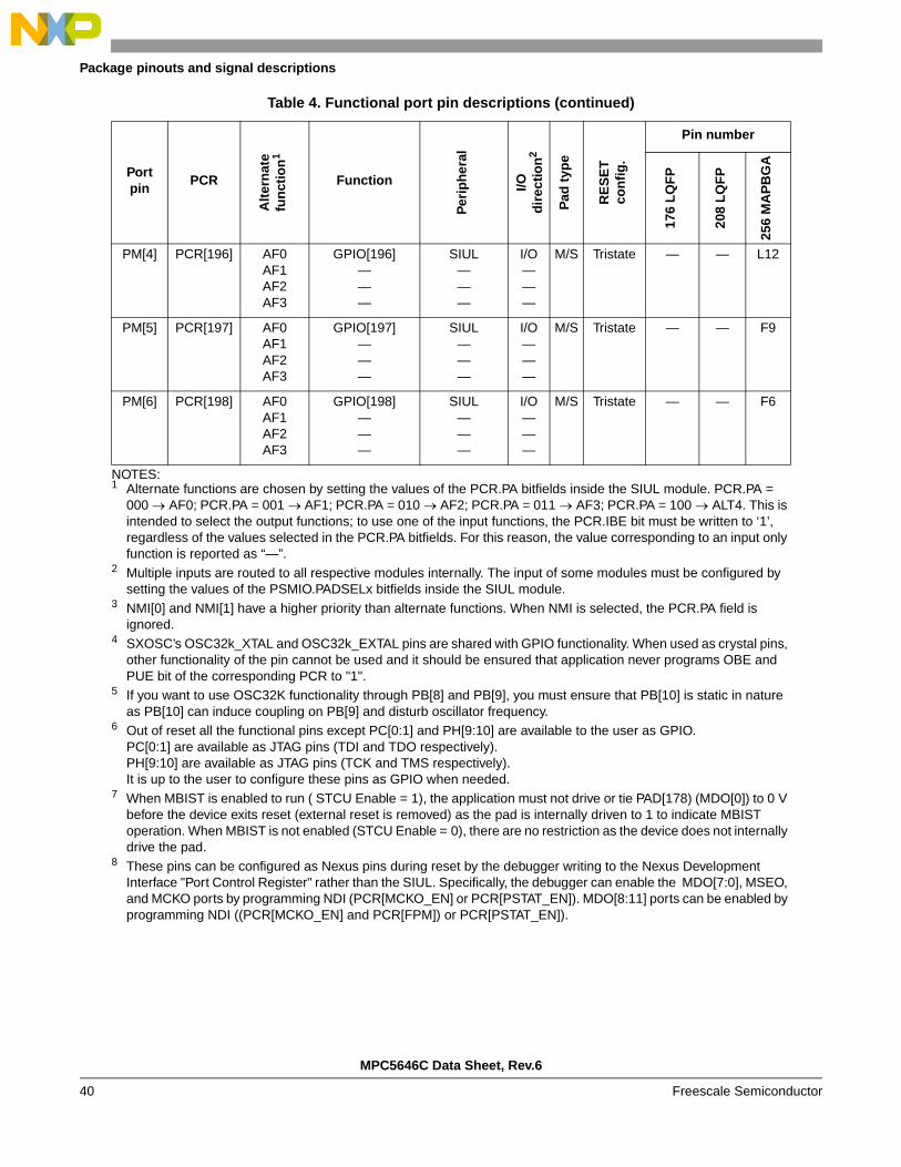
Package pinouts and signal descriptions
PM[4] PCR[196] AF0AF1AF2AF3
GPIO[196]———
SIUL———
I/O———
M/S Tristate — — L12
PM[5] PCR[197] AF0AF1AF2AF3
GPIO[197]———
SIUL———
I/O———
M/S Tristate — — F9
PM[6] PCR[198] AF0AF1AF2AF3
GPIO[198]———
SIUL———
I/O———
M/S Tristate — — F6
NOTES:1 Alternate functions are chosen by setting the values of the PCR.PA bitfields inside the SIUL module. PCR.PA =
000 AF0; PCR.PA = 001 AF1; PCR.PA = 010 AF2; PCR.PA = 011 AF3; PCR.PA = 100 ALT4. This is intended to select the output functions; to use one of the input functions, the PCR.IBE bit must be written to ‘1’, regardless of the values selected in the PCR.PA bitfields. For this reason, the value corresponding to an input only function is reported as “—”.
2 Multiple inputs are routed to all respective modules internally. The input of some modules must be configured by setting the values of the PSMIO.PADSELx bitfields inside the SIUL module.
3 NMI[0] and NMI[1] have a higher priority than alternate functions. When NMI is selected, the PCR.PA field is ignored.
4 SXOSC’s OSC32k_XTAL and OSC32k_EXTAL pins are shared with GPIO functionality. When used as crystal pins, other functionality of the pin cannot be used and it should be ensured that application never programs OBE and PUE bit of the corresponding PCR to "1".
5 If you want to use OSC32K functionality through PB[8] and PB[9], you must ensure that PB[10] is static in nature as PB[10] can induce coupling on PB[9] and disturb oscillator frequency.
6 Out of reset all the functional pins except PC[0:1] and PH[9:10] are available to the user as GPIO.PC[0:1] are available as JTAG pins (TDI and TDO respectively).PH[9:10] are available as JTAG pins (TCK and TMS respectively).It is up to the user to configure these pins as GPIO when needed.
7 When MBIST is enabled to run ( STCU Enable = 1), the application must not drive or tie PAD[178) (MDO[0]) to 0 V before the device exits reset (external reset is removed) as the pad is internally driven to 1 to indicate MBIST operation. When MBIST is not enabled (STCU Enable = 0), there are no restriction as the device does not internally drive the pad.
8 These pins can be configured as Nexus pins during reset by the debugger writing to the Nexus Development Interface "Port Control Register" rather than the SIUL. Specifically, the debugger can enable the MDO[7:0], MSEO, and MCKO ports by programming NDI (PCR[MCKO_EN] or PCR[PSTAT_EN]). MDO[8:11] ports can be enabled by programming NDI ((PCR[MCKO_EN] and PCR[FPM]) or PCR[PSTAT_EN]).
Table 4. Functional port pin descriptions (continued)
Portpin
PCR
Alt
ern
ate
fun
ctio
n1
Function
Per
iph
eral
I/Od
irec
tio
n2
Pad
typ
e
RE
SE
Tco
nfi
g.
Pin number
176
LQ
FP
208
LQ
FP
256
MA
PB
GA
MPC5646C Data Sheet, Rev.6
Freescale Semiconductor40

Electrical Characteristics
4 Electrical CharacteristicsThis section contains electrical characteristics of the device as well as temperature and power considerations.
This product contains devices to protect the inputs against damage due to high static voltages. However, it is advisable to take precautions to avoid application of any voltage higher than the specified maximum rated voltages.
To enhance reliability, unused inputs can be driven to an appropriate logic voltage level (VDD or VSS_HV). This could be done by the internal pull-up and pull-down, which is provided by the product for most general purpose pins.
The parameters listed in the following tables represent the characteristics of the device and its demands on the system.
In the tables where the device logic provides signals with their respective timing characteristics, the symbol “CC” for Controller Characteristics is included in the Symbol column.
In the tables where the external system must provide signals with their respective timing characteristics to the device, the symbol “SR” for System Requirement is included in the Symbol column.
4.1 Parameter classificationThe electrical parameters shown in this supplement are guaranteed by various methods. To give the customer a better understanding, the classifications listed in Table 5 are used and the parameters are tagged accordingly in the tables where appropriate.
NOTEThe classification is shown in the column labeled “C” in the parameter tables where appropriate.
4.2 NVUSRO registerPortions of the device configuration, such as high voltage supply is controlled via bit values in the Non-Volatile User Options Register (NVUSRO). For a detailed description of the NVUSRO register, see MPC5646C Reference Manual.
Table 5. Parameter classifications
Classification tag Tag description
P Those parameters are guaranteed during production testing on each individual device.
C Those parameters are achieved by the design characterization by measuring a statistically relevant sample size across process variations.
T Those parameters are achieved by design characterization on a small sample size from typical devices under typical conditions unless otherwise noted. All values shown in the typical column are within this category.
D Those parameters are derived mainly from simulations.
MPC5646C Data Sheet, Rev.6
Freescale Semiconductor 41

Electrical Characteristics
4.2.1 NVUSRO [PAD3V5V(0)] field description
Table 6 shows how NVUSRO [PAD3V5V(0)] controls the device configuration for VDD_HV_A domain.
The DC electrical characteristics are dependent on the PAD3V5V(0,1) bit value.
4.2.2 NVUSRO [PAD3V5V(1)] field description
Table 7 shows how NVUSRO [PAD3V5V(1)] controls the device configuration the device configuration for VDD_HV_B domain.
The DC electrical characteristics are dependent on the PAD3V5V(0,1) bit value.
4.3 Absolute maximum ratings
Table 6. PAD3V5V(0) field description
Value1
NOTES:1 '1' is delivery value. It is part of shadow flash memory, thus programmable by customer.
Description
0 High voltage supply is 5.0 V
1 High voltage supply is 3.3 V
Table 7. PAD3V5V(1) field description
Value1
NOTES:1 '1' is delivery value. It is part of shadow flash memory, thus programmable by customer.
Description
0 High voltage supply is 5.0 V
1 High voltage supply is 3.3 V
Table 8. Absolute maximum ratings
Symbol Parameter ConditionsValue
UnitMin Max
VSS_HV SR Digital ground on VSS_HV pins
— 0 0 V
VDD_HV_A SR Voltage on VDD_HV_A pins with respect to ground (VSS_HV)
— –0.3 6.0 V
VDD_HV_B1 SR Voltage on VDD_HV_B pins
with respect to common ground (VSS_HV)
— –0.3 6.0 V
VSS_LV SR Voltage on VSS_LV (low voltage digital supply) pins with respect to ground (VSS_HV)
— VSS_HV 0.1 VSS_HV 0.1 V
MPC5646C Data Sheet, Rev.6
Freescale Semiconductor42

Electrical Characteristics
VRC_CTRL2 Base control voltage for
external BCP68 NPN deviceRelative to VDD_LV 0 VDD_LV + 1 V
VSS_ADC SR Voltage on VSS_HV_ADC0, VSS_HV_ADC1 (ADC reference) pin with respect to ground (VSS_HV)
— VSS_HV 0.1 VSS_HV + 0.1 V
VDD_HV_ADC0 SR Voltage on VDD_HV_ADC0 with respect to ground (VSS_HV)
— –0.3 6.0 V
Relative to VDD_HV_A3 VDD_HV_A 0.3 VDD_HV_A+0.3
VDD_HV_ADC14 SR Voltage on VDD_HV_ADC1
with respect to ground (VSS_HV)
— –0.3 6.0 V
Relative to VDD_HV_A2 VDD_HV_A0.3 VDD_HV_A+0.3
VIN SR Voltage on any GPIO pin with respect to ground (VSS_HV)
Relative to VDD_HV_A/HV_B
VDD_HV_A/HV_B0.3
VDD_HV_A/HV_B+0.3
V
IINJPAD SR Injected input current on any pin during overload condition
— –10 10 mA
IINJSUM SR Absolute sum of all injected input currents during overload condition
— –50 50
IAVGSEG5 SR Sum of all the static I/O
current within a supply segment (VDD_HV_A or VDD_HV_B)
VDD = 5.0 V ± 10%, PAD3V5V = 0
70 mA
VDD = 3.3 V ± 10%, PAD3V5V = 1
64
TSTORAGE SR Storage temperature — –556 150 °C
NOTES:1 VDD_HV_B can be independently controlled from VDD_HV_A. These can ramp up or ramp down in any order. Design
is robust against any supply order.2 This voltage is internally generated by the device and no external voltage should be supplied.3 Both the relative and the fixed conditions must be met. For instance: If VDD_HV_A is 5.9 V, VDD_HV_ADC0 maximum
value is 6.0 V then, despite the relative condition, the max value is VDD_HV_A + 0.3 = 6.2 V.4 PA3, PA7, PA10, PA11 and PE12 ADC_1 channels are coming from VDD_HV_B domain hence VDD_HV_ADC1 should
be within ±300 mV of VDD_HV_B when these channels are used for ADC_1.5 Any temperature beyond 125 °C should limit the current to 50 mA (max).6 This is the storage temperature for the flash memory.
Table 8. Absolute maximum ratings (continued)
Symbol Parameter ConditionsValue
UnitMin Max
MPC5646C Data Sheet, Rev.6
Freescale Semiconductor 43

Electrical Characteristics
NOTEStresses exceeding the recommended absolute maximum ratings may cause permanent damage to the device. This is a stress rating only and functional operation of the device at these or any other conditions above those indicated in the operational sections of this specification are not implied. Exposure to absolute maximum rating conditions for extended periods may affect device reliability. During overload conditions (VIN > VDD_HV_A/HV_B or VIN < VSS_HV), the voltage on pins with respect to ground (VSS_HV) must not exceed the recommended values.
4.4 Recommended operating conditions
Table 9. Recommended operating conditions (3.3 V)
Symbol Parameter ConditionsValue
UnitMin Max
VSS_HV SR Digital ground on VSS_HV pins
— 0 0 V
VDD_HV_A1 SR Voltage on VDD_HV_A pins
with respect to ground (VSS_HV)
— 3.0 3.6 V
VDD_HV_B1 SR Voltage on VDD_HV_B pins
with respect to ground (VSS_HV)
— 3.0 3.6 V
VSS_LV2 SR Voltage on VSS_LV (low
voltage digital supply) pins with respect to ground (VSS_HV)
— VSS_HV 0.1 VSS_HV + 0.1 V
VRC_CTRL3 Base control voltage for
external BCP68 NPN deviceRelative to VDD_LV 0 VDD_LV + 1 V
VSS_ADC SR Voltage on VSS_HV_ADC0, VSS_HV_ADC1 (ADC reference) pin with respect to ground (VSS_HV)
— VSS_HV 0.1 VSS_HV + 0.1 V
VDD_HV_ADC04 SR Voltage on VDD_HV_ADC0
with respect to ground (VSS_HV)
— 3.05 3.6 V
Relative to VDD_HV_A6 VDD_HV_A 0.1 VDD_HV_A + 0.1
VDD_HV_ADC17 SR Voltage on VDD_HV_ADC1
with respect to ground (VSS_HV)
— 3.0 3.6 V
Relative to VDD_HV_A6 VDD_HV_A 0.1 VDD_HV_A + 0.1
VIN SR Voltage on any GPIO pin with respect to ground (VSS_HV)
— VSS_HV 0.1 — V
Relative to VDD_HV_A/HV_B
— VDD_HV_A/HV_B+ 0.1
MPC5646C Data Sheet, Rev.6
Freescale Semiconductor44
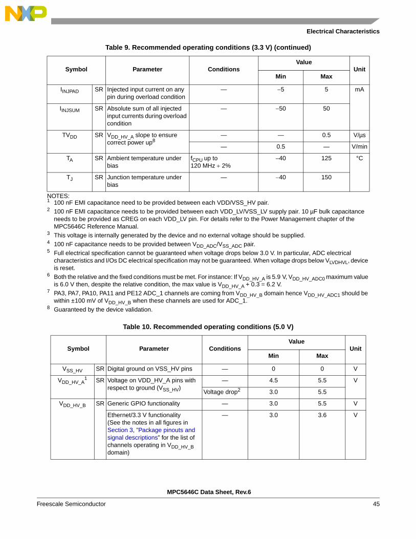
Electrical Characteristics
IINJPAD SR Injected input current on any pin during overload condition
— 5 5 mA
IINJSUM SR Absolute sum of all injected input currents during overload condition
— 50 50
TVDD SR VDD_HV_A slope to ensure correct power up8
— — 0.5 V/µs
— 0.5 — V/min
TA SR Ambient temperature under bias
fCPU up to 120 MHz 2%
–40 125 °C
TJ SR Junction temperature under bias
— 40 150
NOTES:1 100 nF EMI capacitance need to be provided between each VDD/VSS_HV pair.2 100 nF EMI capacitance needs to be provided between each VDD_LV/VSS_LV supply pair. 10 µF bulk capacitance
needs to be provided as CREG on each VDD_LV pin. For details refer to the Power Management chapter of the MPC5646C Reference Manual.
3 This voltage is internally generated by the device and no external voltage should be supplied.4 100 nF capacitance needs to be provided between VDD_ADC/VSS_ADC pair.5 Full electrical specification cannot be guaranteed when voltage drops below 3.0 V. In particular, ADC electrical
characteristics and I/Os DC electrical specification may not be guaranteed. When voltage drops below VLVDHVL, device is reset.
6 Both the relative and the fixed conditions must be met. For instance: If VDD_HV_A is 5.9 V, VDD_HV_ADC0 maximum value is 6.0 V then, despite the relative condition, the max value is VDD_HV_A + 0.3 = 6.2 V.
7 PA3, PA7, PA10, PA11 and PE12 ADC_1 channels are coming from VDD_HV_B domain hence VDD_HV_ADC1 should be within ±100 mV of VDD_HV_B when these channels are used for ADC_1.
8 Guaranteed by the device validation.
Table 10. Recommended operating conditions (5.0 V)
Symbol Parameter ConditionsValue
UnitMin Max
VSS_HV SR Digital ground on VSS_HV pins — 0 0 V
VDD_HV_A1 SR Voltage on VDD_HV_A pins with
respect to ground (VSS_HV)— 4.5 5.5 V
Voltage drop2 3.0 5.5
VDD_HV_B SR Generic GPIO functionality — 3.0 5.5 V
Ethernet/3.3 V functionality(See the notes in all figures in Section 3, ”Package pinouts and signal descriptions” for the list of channels operating in VDD_HV_B domain)
— 3.0 3.6 V
Table 9. Recommended operating conditions (3.3 V) (continued)
Symbol Parameter ConditionsValue
UnitMin Max
MPC5646C Data Sheet, Rev.6
Freescale Semiconductor 45

Electrical Characteristics
VSS_LV3 SR Voltage on VSS_LV (Low voltage
digital supply) pins with respect to ground (VSS_HV)
— VSS_HV – 0.1 VSS_HV + 0.1 V
VRC_CTRL4 Base control voltage for external
BCP68 NPN deviceRelative to
VDD_LV
0 VDD_LV + 1 V
VSS_ADC SR Voltage on VSS_HV_ADC0, VSS_HV_ADC1 (ADC reference) pin with respect to ground (VSS_HV)
— VSS_HV – 0.1 VSS_HV + 0.1 V
VDD_HV_ADC05 SR Voltage on VDD_HV_ADC0 with
respect to ground (VSS_HV)— 4.5 5.5 V
Voltage drop(2) 3.0 5.5
Relative to VDD_HV_A
6VDD_HV_A – 0.1 VDD_HV_A + 0.1
VDD_HV_ADC17 SR Voltage on VDD_HV_ADC1 with
respect to ground (VSS_HV)— 4.5 5.5 V
Voltage drop(2) 3.0 5.5
Relative to VDD_HV_A
6VDD_HV_A 0.1 VDD_HV_A + 0.1
VIN SR Voltage on any GPIO pin with respect to ground (VSS_HV)
— VSS_HV –0.1 — V
Relative to VDD_HV_A/HV_B
— VDD_HV_A/HV_B+ 0.1
IINJPAD SR Injected input current on any pin during overload condition
— –5 5 mA
IINJSUM SR Absolute sum of all injected input currents during overload condition
— –50 50
TVDD SR VDD_HV_A slope to ensure correct power up8
— — 0.5 V/µs
— 0.5 — V/min
TA C-Grade Part SR Ambient temperature under bias — 40 85
°C
TJ C-Grade Part SR Junction temperature under bias — 40 110
TA V-Grade Part SR Ambient temperature under bias — 40 105
TJ V-Grade Part SR Junction temperature under bias — 40 130
TA M-Grade Part SR Ambient temperature under bias — 40 125
TJ M-Grade Part SR Junction temperature under bias — 40 150
NOTES:1 100 nF EMI capacitance need to be provided between each VDD/VSS_HV pair.2 Full device operation is guaranteed by design from 3.0 V–5.5 V. OSC functionality is guaranteed from the entire
range 3.0V–5.5 V, the parametrics measured are at 3.0V and 5.5V (extreme voltage ranges to cover the range of operation). The parametrics might have some variation in the intermediate voltage range, but there is no impact to functionality.
3 100 nF EMI capacitance needs to be provided between each VDD_LV/VSS_LV supply pair. 10 µF bulk capacitance needs to be provided as CREG on each VDD_LV pin.
Table 10. Recommended operating conditions (5.0 V) (continued)
Symbol Parameter ConditionsValue
UnitMin Max
MPC5646C Data Sheet, Rev.6
Freescale Semiconductor46
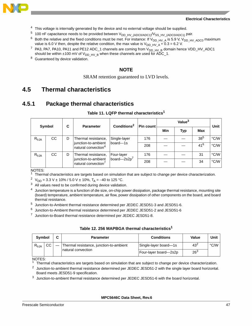
Electrical Characteristics
NOTESRAM retention guaranteed to LVD levels.
4.5 Thermal characteristics
4.5.1 Package thermal characteristics
4 This voltage is internally generated by the device and no external voltage should be supplied.5 100 nF capacitance needs to be provided between VDD_HV_(ADC0/ADC1)/VSS_HV_(ADC0/ADC1) pair.6 Both the relative and the fixed conditions must be met. For instance: If VDD_HV_A is 5.9 V, VDD_HV_ADC0 maximum
value is 6.0 V then, despite the relative condition, the max value is VDD_HV_A + 0.3 = 6.2 V.7 PA3, PA7, PA10, PA11 and PE12 ADC_1 channels are coming from VDD_HV_B domain hence VDD_HV_ADC1
should be within ±100 mV of VDD_HV_B when these channels are used for ADC_1.8 Guaranteed by device validation.
Table 11. LQFP thermal characteristics1
NOTES:1 Thermal characteristics are targets based on simulation that are subject to change per device characterization.
Symbol C Parameter Conditions2
2 VDD = 3.3 V ± 10% / 5.0 V ± 10%, TA = 40 to 125 °C.
Pin countValue3
3 All values need to be confirmed during device validation.
UnitMin Typ Max
RJA CC D Thermal resistance, junction-to-ambient natural convection4
4 Junction temperature is a function of die size, on-chip power dissipation, package thermal resistance, mounting site (board) temperature, ambient temperature, air flow, power dissipation of other components on the board, and board thermal resistance.
Single-layer board—1s
176 — — 385
5 Junction-to-Ambient thermal resistance determined per JEDEC JESD51-3 and JESD51-6.
°C/W
208 — — 416
6 Junction-to-Ambient thermal resistance determined per JEDEC JESD51-2 and JESD51-6
°C/W
RJA CC D Thermal resistance, junction-to-ambient natural convection7
Four-layer board—2s2p7
7 Junction-to-Board thermal resistance determined per JEDEC JESD51-8.
176 — — 31 °C/W
208 — — 34 °C/W
Table 12. 256 MAPBGA thermal characteristics1
NOTES:1 Thermal characteristics are targets based on simulation that are subject to change per device characterization.
Symbol C Parameter Conditions Value Unit
RJA CC — Thermal resistance, junction-to-ambient natural convection
Single-layer board—1s 432
2 Junction-to-ambient thermal resistance determined per JEDEC JESD51-2 with the single layer board horizontal. Board meets JESD51-9 specification.
°C/W
Four-layer board—2s2p 263
3 Junction-to-ambient thermal resistance determined per JEDEC JESD51-6 with the board horizontal.
MPC5646C Data Sheet, Rev.6
Freescale Semiconductor 47

Electrical Characteristics
4.5.2 Power considerations
The average chip-junction temperature, TJ, in degrees Celsius, may be calculated using Equation 1:
TJ = TA + (PD RJA) Eqn. 1
Where:
TA is the ambient temperature in °C.
RJA is the package junction-to-ambient thermal resistance, in °C/W.
PD is the sum of PINT and PI/O (PD = PINT + PI/O).
PINT is the product of IDD and VDD, expressed in watts. This is the chip internal power.
PI/O represents the power dissipation on input and output pins; user determined.
Most of the time for the applications, PI/O< PINT and may be neglected. On the other hand, PI/O may be significant, if the device is configured to continuously drive external modules and/or memories.
An approximate relationship between PD and TJ (if PI/O is neglected) is given by:
PD = K / (TJ + 273 °C) Eqn. 2
Therefore, solving equations 1 and 2:
K = PD (TA + 273 °C) + RJA PD2 Eqn. 3
Where:
K is a constant for the particular part, which may be determined from Equation 3 by measuring PD (at equilibrium) for a known TA. Using this value of K, the values of PD and TJ may be obtained by solving equations 1 and 2 iteratively for any value of TA.
4.6 I/O pad electrical characteristics
4.6.1 I/O pad types
The device provides four main I/O pad types depending on the associated alternate functions:
• Slow pads—These pads are the most common pads, providing a good compromise between transition time and low electromagnetic emission.
• Medium pads—These pads provide transition fast enough for the serial communication channels with controlled current to reduce electromagnetic emission.
• Fast pads—These pads provide maximum speed. These are used for improved Nexus debugging capability.
• Input only pads—These pads are associated to ADC channels and 32 kHz low power external crystal oscillator providing low input leakage.
• Low power pads—These pads are active in standby mode for wakeup source.
Also, medium/slow and fast/medium pads are available in design which can be configured to behave like a slow/medium and medium/fast pads depending upon the slew-rate control.
MPC5646C Data Sheet, Rev.6
Freescale Semiconductor48

Electrical Characteristics
Medium and fast pads can use slow configuration to reduce electromagnetic emission, at the cost of reducing AC performance.
4.6.2 I/O input DC characteristics
Table 13 provides input DC electrical characteristics as described in Figure 5.
Figure 5. I/O input DC electrical characteristics definition
Table 13. I/O input DC electrical characteristics
Symbol C Parameter Conditions1
NOTES:1 VDD = 3.3 V ± 10% / 5.0 V ± 10%, TA = 40 to 125 °C, unless otherwise specified.
Value2
UnitMin Typ Max
VIH SR P Input high level CMOS (Schmitt Trigger)
— 0.65VDD — VDD + 0.4 V
VIL SR P Input low level CMOS (Schmitt Trigger)
— 0.3 — 0.35VDD
VHYS CC C Input hysteresis CMOS (Schmitt Trigger)
— 0.1VDD — —
ILKG CC P Digital input leakage No injection on adjacent pin
TA = 40 °C — 2 — nA
P TA = 25 °C — 2 —
D TA = 105 °C — 12 500
P TA = 125 °C — 70 1000
WFI SR P Width of input pulse rejected byanalog filter3
— — — 404 ns
WNFI SR P Width of input pulse accepted byanalog filter(3)
— 10004 — — ns
VIL
VIN
VIH
PDIx = ‘1
VDD
VHYS
(GPDI register of SIUL)
PDIx = ‘0’
MPC5646C Data Sheet, Rev.6
Freescale Semiconductor 49

Electrical Characteristics
4.6.3 I/O output DC characteristics
The following tables provide DC characteristics for bidirectional pads:
• Table 14 provides weak pull figures. Both pull-up and pull-down resistances are supported.
• Table 15 provides output driver characteristics for I/O pads when in SLOW configuration.
• Table 16 provides output driver characteristics for I/O pads when in MEDIUM configuration.
• Table 17 provides output driver characteristics for I/O pads when in FAST configuration.
2 VDD as mentioned in the table is VDD_HV_A/VDD_HV_B. All values need to be confirmed during device validation.3 Analog filters are available on all wakeup lines.4 The width of input pulse in between 40 ns to 1000 ns is indeterminate. It may pass the noise or may not depending
on silicon sample to sample variation.
Table 14. I/O pull-up/pull-down DC electrical characteristics
Symbol C Parameter Conditions1,2
NOTES:1 VDD = 3.3 V ± 10% / 5.0 V ± 10%, TA = 40 to 125 °C, unless otherwise specified.2 VDD as mentioned in the table is VDD_HV_A/VDD_HV_B.
ValueUnit
Min Typ Max
|IWPU| CC P Weak pull-up current absolute value
VIN = VIL, VDD = 5.0 V ± 10%
PAD3V5V = 0 10 — 150 µA
C PAD3V5V = 13
3 The configuration PAD3V5 = 1 when VDD = 5 V is only a transient configuration during power-up. All pads but RESET and Nexus output (MDOx, EVTO, MCKO) are configured in input or in high impedance state.
10 — 250
P VIN = VIL, VDD = 3.3 V ± 10%
PAD3V5V = 1 10 — 150
|IWPD| CC P Weak pull-down current absolute value
VIN = VIH, VDD = 5.0 V ± 10%
PAD3V5V = 0 10 — 150 µA
C PAD3V5V = 1 10 — 250
P VIN = VIH, VDD = 3.3 V ± 10%
PAD3V5V = 1 10 — 150
Table 15. SLOW configuration output buffer electrical characteristics
Symbol C Parameter Conditions1,2Value
UnitMin Typ Max
VOH CC P Output high levelSLOW configuration
Push Pull IOH = 3 mA,VDD = 5.0 V ± 10%, PAD3V5V = 0
0.8VDD — — V
C IOH = 3 mA,VDD = 5.0 V ± 10%, PAD3V5V = 13
0.8VDD — —
P IOH = 1.5 mA,VDD = 3.3 V ± 10%, PAD3V5V = 1
VDD 0.8 — —
MPC5646C Data Sheet, Rev.6
Freescale Semiconductor50

Electrical Characteristics
VOL CC P Output low levelSLOW configuration
Push Pull IOL = 3 mA,VDD = 5.0 V ± 10%, PAD3V5V = 0
— — 0.1VDD V
C IOL = 3 mA,VDD = 5.0 V ± 10%, PAD3V5V = 1(3)
— — 0.1VDD
P IOL = 1.5 mA,VDD = 3.3 V ± 10%, PAD3V5V = 1
— — 0.5
NOTES:1 VDD = 3.3 V ± 10% / 5.0 V ± 10%, TA = 40 to 125 °C, unless otherwise specified.2 VDD as mentioned in the table is VDD_HV_A/VDD_HV_B. 3 The configuration PAD3V5 = 1 when VDD = 5 V is only a transient configuration during power-up. All pads but
RESET and Nexus output (MDOx, EVTO, MCKO) are configured in input or in high impedance state.
Table 16. MEDIUM configuration output buffer electrical characteristics
Symbol C Parameter Conditions1,2
NOTES:1 VDD = 3.3 V ± 10% / 5.0 V ± 10%, TA = 40 to 125 °C, unless otherwise specified.2 VDD as mentioned in the table is VDD_HV_A/VDD_HV_B.
ValueUnit
Min Typ Max
VOH CC C Output high levelMEDIUM configuration
Push Pull IOH = 3 mA,VDD = 5.0 V ± 10%, PAD3V5V = 0
0.8VDD — —
VC IOH = 1.5 mA,VDD = 5.0 V ± 10%, PAD3V5V = 13
3 The configuration PAD3V5 = 1 when VDD = 5 V is only a transient configuration during power-up. All pads but RESET and Nexus output (MDOx, EVTO, MCKO) are configured in input or in high impedance state.
0.8VDD — —
C IOH = 2 mA,VDD = 3.3 V ± 10%, PAD3V5V = 1
VDD 0.8 — —
VOL CC C Output low levelMEDIUM configuration
Push Pull IOL = 3 mA,VDD = 5.0 V ± 10%, PAD3V5V = 0
— — 0.2VDD
VC IOL = 1.5 mA,VDD = 5.0 V ± 10%, PAD3V5V = 1(3)
— — 0.1VDD
C IOL = 2 mA,VDD = 3.3 V ± 10%, PAD3V5V = 1
— — 0.5
Table 15. SLOW configuration output buffer electrical characteristics (continued)
Symbol C Parameter Conditions1,2Value
UnitMin Typ Max
MPC5646C Data Sheet, Rev.6
Freescale Semiconductor 51

Electrical Characteristics
4.6.4 Output pin transition times
Table 17. FAST configuration output buffer electrical characteristics
Symbol C Parameter Conditions1,2
NOTES:1 VDD = 3.3 V ± 10% / 5.0 V ± 10%, TA = 40 to 125 °C, unless otherwise specified.2 VDD as mentioned in the table is VDD_HV_A/VDD_HV_B.
ValueUnit
Min Typ Max
VOH CC P Output high levelFAST configuration
Push Pull IOH = 14 mA,VDD = 5.0 V ± 10%, PAD3V5V = 0
0.8VDD — — V
C IOH = 7 mA,VDD = 5.0 V ± 10%, PAD3V5V = 13
3 The configuration PAD3V5 = 1 when VDD = 5 V is only a transient configuration during power-up. All pads but RESET and Nexus outputs (MDOx, EVTO, MCKO) are configured in input or in high impedance state.
0.8VDD — —
C IOH = 11 mA,VDD = 3.3 V ± 10%, PAD3V5V = 1
VDD 0.8 — —
VOL CC P Output low levelFAST configuration
Push Pull IOL = 14 mA,VDD = 5.0 V ± 10%, PAD3V5V = 0
— — 0.1VDD V
C IOL = 7 mA,VDD = 5.0 V ± 10%, PAD3V5V = 1(3)
— — 0.1VDD
C IOL = 11 mA,VDD = 3.3 V ± 10%, PAD3V5V = 1
— — 0.5
Table 18. Output pin transition times
Symbol C Parameter Conditions1,2Value3
UnitMin Typ Max
Ttr CC D Output transition time output pin4
SLOW configuration
CL = 25 pF VDD = 5.0 V ± 10%,PAD3V5V = 0
— — 50 ns
T CL = 50 pF — — 100
D CL = 100 pF — — 125
D CL = 25 pF VDD = 3.3 V ± 10%, PAD3V5V = 1
— — 40
T CL = 50 pF — — 50
D CL = 100 pF — — 75
MPC5646C Data Sheet, Rev.6
Freescale Semiconductor52

Electrical Characteristics
4.6.5 I/O pad current specification
The I/O pads are distributed across the I/O supply segment. Each I/O supply is associated to a VDD/VSS_HV supply pair as described in Table 19.
Table 20 provides I/O consumption figures.
In order to ensure device reliability, the average current of the I/O on a single segment should remain below the IAVGSEG maximum value.
In order to ensure device functionality, the sum of the dynamic and static current of the I/O on a single segment should remain below the IDYNSEG maximum value.
Ttr CC D Output transition time output pin(4)
MEDIUM configuration
CL = 25 pF VDD = 5.0 V ± 10%, PAD3V5V = 0SIUL.PCRx.SRC = 1
— — 10 ns
T CL = 50 pF — — 20
D CL = 100 pF — — 40
D CL = 25 pF VDD = 3.3 V ± 10%, PAD3V5V = 1SIUL.PCRx.SRC = 1
— — 12
T CL = 50 pF — — 25
D CL = 100 pF — — 40
Ttr CC D Output transition time output pin(4)
FAST configuration
CL = 25 pF VDD = 5.0 V ± 10%, PAD3V5V = 0
— — 4 ns
CL = 50 pF — — 6
CL = 100 pF — — 12
CL = 25 pF VDD = 3.3 V ± 10%, PAD3V5V = 1
— — 4
CL = 50 pF — — 7
CL = 100 pF — — 12
NOTES:1 VDD = 3.3 V ± 10% / 5.0 V ± 10%, TA = 40 to 125 °C, unless otherwise specified.2 VDD as mentioned in the table is VDD_HV_A/VDD_HV_B. 3 All values need to be confirmed during device validation.4 CL includes device and package capacitances (CPKG < 5 pF).
Table 19. I/O supplies
Package I/O Supplies
256 MAPBGA Equivalent to 208-pin LQFP segment pad distribution + G6, G11, H11, J11
208 LQFP pin6 (VDD_HV_A)pin7 (VSS_HV)
pin27 (VDD_HV_A)pin28 (VSS_HV)
pin73 (VSS_HV)pin75 (VDD_HV_A)
pin101 (VDD_HV_A)pin102 (VSS_HV)
pin132 (VSS_HV)pin133 (VDD_HV_A)
pin147 (VSS_HV)pin148 (VDD_HV_B)
pin174 (VSS_HV)pin175 (VDD_HV_A)
—
Table 18. Output pin transition times (continued)
Symbol C Parameter Conditions1,2Value3
UnitMin Typ Max
MPC5646C Data Sheet, Rev.6
Freescale Semiconductor 53

Electrical Characteristics
176 LQFP pin6 (VDD_HV_A)pin7(VSS_HV)
pin27 (VDD_HV_A)pin28(VSS_HV)
pin57 (VSS_HV) pin59 (VDD_HV_A)
pin85 (VDD_HV_A)pin86 (VSS_HV)
pin123 (VSS_HV) pin124 (VDD_HV_B)
pin150 (VSS_HV) pin151 (VDD_HV_A)
— —
Table 20. I/O consumption
Symbol C Parameter Conditions1,2Value3
UnitMin Typ Max
ISWTSLW,4 CC D Peak I/O current for
SLOW configurationCL = 25 pF VDD = 5.0 V ± 10%,
PAD3V5V = 0— — 19.9
mAVDD = 3.3 V ± 10%,PAD3V5V = 1
— — 15.5
ISWTMED(4) CC D Peak I/O current for
MEDIUM configuration
CL = 25 pF VDD = 5.0 V ± 10%,PAD3V5V = 0
— — 28.8
mAVDD = 3.3 V ± 10%,PAD3V5V = 1
— — 16.3
ISWTFST(4) CC D Peak I/O current for
FAST configurationCL = 25 pF VDD = 5.0 V ± 10%,
PAD3V5V = 0— — 113.5
mAVDD = 3.3 V ± 10%,PAD3V5V = 1
— — 52.1
IRMSSLW CC D Root mean square I/O current for SLOW configuration
CL = 25 pF, 2 MHz VDD = 5.0 V ± 10%,PAD3V5V = 0
— — 2.22
mA
CL = 25 pF, 4 MHz — — 3.13
CL = 100 pF, 2 MHz — — 6.54
CL = 25 pF, 2 MHz VDD = 3.3 V ± 10%,PAD3V5V = 1
— — 1.51
CL = 25 pF, 4 MHz — — 2.14
CL = 100 pF, 2 MHz — — 4.33
IRMSMED CC D Root mean square I/O current for MEDIUM configuration
CL = 25 pF, 13 MHz VDD = 5.0 V ± 10%, PAD3V5V = 0
— — 6.5 mA
CL = 25 pF, 40 MHz — — 13.32
CL = 100 pF, 13 MHz — — 18.26
CL = 25 pF, 13 MHz VDD = 3.3 V ± 10%, PAD3V5V = 1
— — 4.91
CL = 25 pF, 40 MHz — — 8.47
CL = 100 pF, 13 MHz — — 10.94
IRMSFST CC D Root mean square I/O current for FAST configuration
CL = 25 pF, 40 MHz VDD = 5.0 V ± 10%, PAD3V5V = 0
— — 21.05 mA
CL = 25 pF, 64 MHz — — 33
CL = 100 pF, 40 MHz — — 55.77
CL = 25 pF, 40 MHz VDD = 3.3 V ± 10%, PAD3V5V = 1
— — 14
CL = 25 pF, 64 MHz — — 20
CL = 100 pF, 40 MHz — — 34.89
Table 19. I/O supplies (continued)
Package I/O Supplies
MPC5646C Data Sheet, Rev.6
Freescale Semiconductor54

Electrical Characteristics
4.7 RESET electrical characteristicsThe device implements a dedicated bidirectional RESET pin.
Figure 6. Start-up reset requirements
IAVGSEG SR D Sum of all the static I/O current within a supply segment
VDD = 5.0 V ± 10%, PAD3V5V = 0 — — 70 mA
VDD = 3.3 V ± 10%, PAD3V5V = 1 — — 654
NOTES:1 VDD = 3.3 V ± 10% / 5.0 V ± 10%, TA = 40 to 125 °C, unless otherwise specified.2 VDD as mentioned in the table is VDD_HV_A/VDD_HV_B. 3 All values need to be confirmed during device validation.4 Stated maximum values represent peak consumption that lasts only a few ns during I/O transition.
Table 20. I/O consumption (continued)
Symbol C Parameter Conditions1,2Value3
UnitMin Typ Max
VIL
VDD_HV_A
device reset forced by RESET
VDDMIN
RESET
VIH
device start-up phase
MPC5646C Data Sheet, Rev.6
Freescale Semiconductor 55

Electrical Characteristics
Figure 7. Noise filtering on reset signal
Table 21. Reset electrical characteristics
Symbol C Parameter Conditions1Value2
UnitMin Typ Max
VIH SR P Input High Level CMOS (Schmitt Trigger)
— 0.65VDD — VDD + 0.4 V
VIL SR P Input low Level CMOS (Schmitt Trigger)
— 0.3 — 0.35VDD V
VHYS CC C Input hysteresis CMOS (Schmitt Trigger)
— 0.1VDD — — V
VOL CC P Output low level Push Pull, IOL = 2 mA,VDD = 5.0 V ± 10%, PAD3V5V = 0(recommended)
— — 0.1VDD V
Push Pull, IOL = 1 mA,VDD = 5.0 V ± 10%, PAD3V5V = 13
— — 0.1VDD
Push Pull, IOL = 1 mA,VDD = 3.3 V ± 10%, PAD3V5V = 1 (recommended)
— — 0.5
VRESET
VIL
VIH
VDD
filtered by hysteresis
filtered by lowpass filter
WFRST
WNFRST
hw_rst
‘1’
‘0’filtered by lowpass filter
WFRST
unknown resetstate device under hardware reset
MPC5646C Data Sheet, Rev.6
Freescale Semiconductor56

Electrical Characteristics
4.8 Power management electrical characteristics
4.8.1 Voltage regulator electrical characteristics
The device implements an internal voltage regulator to generate the low voltage core supply VDD_LV from the high voltage supply VDD_HV_A. The following supplies are involved:
• HV: High voltage external power supply for voltage regulator module. This must be provided externally through VDD_HV_A power pin.
• LV: Low voltage internal power supply for core, FMPLL and Flash digital logic. This is generated by the on-chip VREG with an external ballast (BCP68 NPN device). It is further split into four main domains to ensure noise isolation between critical LV modules within the device:
— LV_COR: Low voltage supply for the core. It is also used to provide supply for FMPLL through double bonding.
Ttr CC D Output transition time output pin4
MEDIUM configuration
CL = 25 pF,VDD = 5.0 V ± 10%, PAD3V5V = 0
— — 10 ns
CL = 50 pF,VDD = 5.0 V ± 10%, PAD3V5V = 0
— — 20
CL = 100 pF,VDD = 5.0 V ± 10%, PAD3V5V = 0
— — 40
CL = 25 pF,VDD = 3.3 V ± 10%, PAD3V5V = 1
— — 12
CL = 50 pF,VDD = 3.3 V ± 10%, PAD3V5V = 1
— — 25
CL = 100 pF,VDD = 3.3 V ± 10%, PAD3V5V = 1
— — 40
WFRST SR P Reset input filtered pulse — — — 40 ns
WNFRST SR P Reset input not filtered pulse
— 1000 — — ns
|IWPU| CC P Weak pull-up current absolute value
VDD = 3.3 V ± 10%, PAD3V5V = 1 10 — 150 µA
VDD = 5.0 V ± 10%, PAD3V5V = 0 10 — 150
VDD = 5.0 V ± 10%, PAD3V5V = 15 10 — 250
NOTES:1 VDD = 3.3 V ± 10% / 5.0 V ± 10%, TA = 40 to 125 °C, unless otherwise specified.2 VDD as mentioned in the table is VDD_HV_A/VDD_HV_B. All values need to be confirmed during device validation.3 This is a transient configuration during power-up, up to the end of reset PHASE2 (refer to the RGM module section
of the device Reference Manual).4 CL includes device and package capacitance (CPKG < 5 pF).5 The configuration PAD3V5 = 1 when VDD = 5 V is only transient configuration during power-up. All pads but
RESET and Nexus output (MDOx, EVTO, MCKO) are configured in input or in high impedance state.
Table 21. Reset electrical characteristics (continued)
Symbol C Parameter Conditions1Value2
UnitMin Typ Max
MPC5646C Data Sheet, Rev.6
Freescale Semiconductor 57

Electrical Characteristics
— LV_CFLA0/CFLA1: Low voltage supply for the two code Flash modules. It is shorted with LV_COR through double bonding.
— LV_DFLA: Low voltage supply for data Flash module. It is shorted with LV_COR through double bonding.
— LV_PLL: Low voltage supply for FMPLL. It is shorted to LV_COR through double bonding.
Figure 8. Voltage regulator capacitance connection
The internal voltage regulator requires external bulk capacitance (CREGn) to be connected to the device to provide a stable low voltage digital supply to the device. Also required for stability is the CDEC2 capacitor at ballast collector. This is needed to minimize sharp injection current when ballast is turning ON. Apart from the bulk capacitance, user should connect EMI/decoupling cap (CREGP) at each VDD_LV/VSS_LV pin pair.
4.8.1.1 Recommendations
• The external NPN driver must be BCP68 type.
• VDD_LV should be implemented as a power plane from the emitter of the ballast transistor.
32 KB 56 KBSplitSplit
CTRL CTRL
Split
CTRL
PD0 (always on domain)
PD1 Switchable Domain
HPREG
LPREG
HPVDD
LPVDD
VDD_LV
VSS_LVOff chip
BCP68
40 f
HPVDDLPVDD
sw1 (<0.1)
8 KB
PD
0 Lo
gic
VDD_BV VDD_HV_A VSS_HV
100 nf
(FMPLL, Flash)
VDD_LV VDD_LV VDD_LVVSS_LV VSS_LV VSS_LV
100 nf 100 nf 100 nf
VRC_CTRL
(CREGn)
Chip Boundary
10 f
(CDEC2)
(4 10 f)
NPN driver
1) All VSS_LV pins must be grounded, as shown for VSS_HV pin.
MPC5646C Data Sheet, Rev.6
Freescale Semiconductor58

Electrical Characteristics
• 10 F capacitors should be connected to the 4 pins closest to the outside of the package and should be evenly distributed around the package. For BGA packages, the balls should be used are D8, H14, R9, J3–one cap on each side of package.
— There should be a track direct from the capacitor to this pin (pin also connects to VDD_LV plane). The tracks ESR should be less than 100 m.
— The remaining VDD_LV pins (exact number will vary with package) should be decoupled with 0.1 F caps, connected to the pin as per 10 F.
(see Section 4.4, ”Recommended operating conditions”).
4.8.2 VDD_BV options• Option 1: VDD_BV shared with VDD_HV_A
VDD_BV must be star routed from VDD_HV_A from the common source. This is to eliminate ballast noise injection on the MCU.
• Option 2: VDD_BV independent of the MCU supply
VDD_BV > 2.6 V for correct functionality. The device is not monitoring this supply hence the external component must meet the 2.6 V criteria through external monitoring if required.
Table 22. Voltage regulator electrical characteristics
Symbol C Parameter Conditions1Value2
UnitMin Typ Max
CREGn SR — External ballast stability capacitance — 40 — 60 F
RREG SR — Stability capacitor equivalent serial resistance
— — — 0.2
CREGP SR — Decoupling capacitance (Close to the pin)
VDD_HV_A/HV_B/VSS_HV pair
100 — nF
VDD_LV/VSS_LV pair 100 — nF
CDEC2 SR — Stability capacitance regulator supply (Close to the ballast collector)
VDD_BV/VSS_HV 10 — 40 F
VMREG CC P Main regulator output voltage Before trimming — 1.32 — V
After trimmingTA = 25 °C
1.20 1.28 —
IMREG SR — Main regulator current provided to VDD_LV domain
— — — 350 mA
IMREGINT CC D Main regulator module current consumption
IMREG = 200 mA — — 2 mA
IMREG = 0 mA — — 1
VLPREG CC P Low power regulator output voltage After trimmingTA = 25 °C
1.21 1.27 — V
ILPREG SR — Low power regulator current provided to VDD_LV domain
—— — 50 mA
MPC5646C Data Sheet, Rev.6
Freescale Semiconductor 59

Electrical Characteristics
4.8.3 Voltage monitor electrical characteristics
The device implements a Power-on Reset module to ensure correct power-up initialization, as well as four low voltage detectors to monitor the VDD_HV_A and the VDD_LV voltage while device is supplied:
• POR monitors VDD_HV_A during the power-up phase to ensure device is maintained in a safe reset state
• LVDHV3 monitors VDD_HV_A to ensure device is reset below minimum functional supply
• LVDHV5 monitors VDD_HV_A when application uses device in the 5.0 V±10% range
• LVDLVCOR monitors power domain No. 1 (PD1)
• LVDLVBKP monitors power domain No. 0 (PD0). VDD_LV is same as PD0 supply.
NOTEWhen enabled, PD2 (RAM retention) is monitored through LVD_DIGBKP.
ILPREGINT CC D Low power regulator module current consumption
ILPREG = 15 mA;TA = 55 °C
— — 600 A
— ILPREG = 0 mA;TA = 55 °C
— 20 —
IVREGREF CC D Main LVDs and reference current consumption (low power and main regulator switched off)
TA = 55 °C — 2 — A
IVREDLVD12 CC D Main LVD current consumption (switch-off during standby)
TA = 55 °C — 1 — A
IDD_HV_A CC D In-rush current on VDD_BV during power-up
— — — 6003 mA
NOTES:1 VDD_HV_A = 3.3 V ± 10% / 5.0 V ± 10%, TA = 40 to 125 °C, unless otherwise specified.2 All values need to be confirmed during device validation.3 Inrush current is seen more like steps of 600 mA peak. The startup of the regulator happens in steps of 50 mV in
~25 steps to reach ~1.2 V VDD_LV. Each step peak current is within 600 mA
Table 22. Voltage regulator electrical characteristics (continued)
Symbol C Parameter Conditions1Value2
UnitMin Typ Max
MPC5646C Data Sheet, Rev.6
Freescale Semiconductor60

Electrical Characteristics
Figure 9. Low voltage monitor vs. Reset
4.9 Low voltage domain power consumptionTable 24 provides DC electrical characteristics for significant application modes. These values are indicative values; actual consumption depends on the application.
Table 23. Low voltage monitor electrical characteristics
Symbol C Parameter Conditions1
NOTES:1 VDD = 3.3 V ± 10% / 5.0 V ± 10%, TA = 40 to 125 °C, unless otherwise specified.
Value2
2 All values need to be confirmed during device validation.
UnitMin Typ Max
VPORUP SR P Supply for functional POR module — 1.0 — 5.5
V
VPORH CC P Power-on reset threshold — 1.5 — 2.6
VLVDHV3H CC T LVDHV3 low voltage detector high threshold — 2.7 — 2.85
VLVDHV3L CC T LVDHV3 low voltage detector low threshold — 2.6 — 2.74
VLVDHV5H CC T LVDHV5 low voltage detector high threshold — 4.3 — 4.5
VLVDHV5L CC T LVDHV5 low voltage detector low threshold — 4.2 — 4.4
VLVDLVCORL CC P LVDLVCOR low voltage detector low threshold TA = 25 °C,after trimming
1.12 1.145 1.17
VLVDLVBKPL CC P LVDLVBKP low voltage detector low threshold 1.12 1.145 1.17
VDDHV/LV
VLVDHVxH/LVxH
RESET
VLVDHVxL/LVxL
MPC5646C Data Sheet, Rev.6
Freescale Semiconductor 61

Electrical Characteristics
Table 24. Low voltage power domain electrical characteristics1
NOTES:1 Except for IDDMAX, all the current values are total current drawn from VDD_HV_A.
Symbol C Parameter Conditions2
2 VDD = 3.3 V ± 10% / 5.0 V ± 10%, TA = 40 to 125 °C, unless otherwise specified All temperatures are based on an ambient temperature.
ValueUnit
Min Typ3
3 Target typical current consumption for the following typical operating conditions and configuration. Process = typical, Voltage = 1.2 V.
Max4
4 Target maximum current consumption for mode observed under typical operating conditions. Process = Fast, Voltage = 1.32 V.
IDDMAX5
5 Running consumption is given on voltage regulator supply (VDDREG). It does not include consumption linked to I/Os toggling. This value is highly dependent on the application. The given value is thought to be a worst case value with all cores and peripherals running, and code fetched from code flash while modify operation on-going on data flash. It is to be noticed that this value can be significantly reduced by application: switch-off not used peripherals (default), reduce peripheral frequency through internal prescaler, fetch from RAM most used functions, use low power mode when possible.
CC D RUN mode maximum average current
— — 210 3006,7
6 Higher current may sunk by device during power-up and standby exit. Please refer to in rush current in Table 22.7 Maximum “allowed” current is package dependent.
mA
IDDRUN CC P RUN mode typical average current8
8 Only for the “P” classification: Code fetched from RAM: Serial IPs CAN and LIN in loop back mode, DSPI as Master, PLL as system Clock (4 x Multiplier) peripherals on (eMIOS/CTU/ADC) and running at max frequency, periodic SW/WDG timer reset enabled. RUN current measured with typical application with accesses on both code flash and RAM.
at 120 MHz TA = 25 °C — 150 2009 mA
D at 80 MHz TA = 25 °C — 1108 15010 mA
C at 120 MHz TA = 125 °C — 180 270 mA
IDDHALT CC P HALT mode current11 at 120 MHz TA = 25 °C — 20 27 mA
C at 120 MHz TA = 125 °C — 35 113 mA
IDDSTOP CC P STOP mode current12 No clocks active TA = 25 °C — 0.4 3 mA
C TA = 125 °C — 16 95 mA
IDDSTDBY3(96 KB RAM
retained)
CC P STANDBY3 mode current13
No clocks active TA = 25 °C — 50 99 µA
C TA = 125 °C — 630 3200 µA
IDDSTDBY2(64 KB RAM
retained)
CC C STANDBY2 mode current14
No clocks active TA = 25 °C — 40 94 µA
C TA = 125 °C — 500 2500 µA
IDDSTDBY1(8 KB RAM retained)
CC C STANDBY1 mode current15
No clocks active TA = 25 °C — 25 87 µA
C TA = 125 °C — 230 1250 µA
Adders in LP mode
CC T 32 KHz OSC — TA = 25 °C — — 5 µA
4–40 MHz OSC — TA = 25 °C — — 3 mA
16 MHz IRC — TA = 25 °C — — 500 µA
128 KHz IRC — TA = 25 °C — — 5 µA
MPC5646C Data Sheet, Rev.6
Freescale Semiconductor62
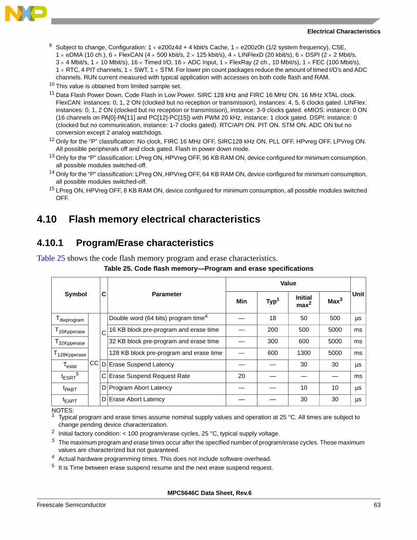
Electrical Characteristics
4.10 Flash memory electrical characteristics
4.10.1 Program/Erase characteristics
Table 25 shows the code flash memory program and erase characteristics.
9 Subject to change, Configuration: 1 e200z4d + 4 kbit/s Cache, 1 e200z0h (1/2 system frequency), CSE, 1 eDMA (10 ch.), 6 FlexCAN (4 500 kbit/s, 2 125 kbit/s), 4 LINFlexD (20 kbit/s), 6 DSPI (2 2 Mbit/s, 3 4 Mbit/s, 1 10 Mbit/s), 16 Timed I/O, 16 ADC Input, 1 FlexRay (2 ch., 10 Mbit/s), 1 FEC (100 Mbit/s), 1 RTC, 4 PIT channels, 1 SWT, 1 STM. For lower pin count packages reduce the amount of timed I/O’s and ADC channels. RUN current measured with typical application with accesses on both code flash and RAM.
10 This value is obtained from limited sample set.11 Data Flash Power Down. Code Flash in Low Power. SIRC 128 kHz and FIRC 16 MHz ON. 16 MHz XTAL clock.
FlexCAN: instances: 0, 1, 2 ON (clocked but no reception or transmission), instances: 4, 5, 6 clocks gated. LINFlex: instances: 0, 1, 2 ON (clocked but no reception or transmission), instance: 3-9 clocks gated. eMIOS: instance: 0 ON (16 channels on PA[0]-PA[11] and PC[12]-PC[15]) with PWM 20 kHz, instance: 1 clock gated. DSPI: instance: 0 (clocked but no communication, instance: 1-7 clocks gated). RTC/API ON. PIT ON. STM ON. ADC ON but no conversion except 2 analog watchdogs.
12 Only for the “P” classification: No clock, FIRC 16 MHz OFF, SIRC128 kHz ON, PLL OFF, HPvreg OFF, LPVreg ON. All possible peripherals off and clock gated. Flash in power down mode.
13 Only for the “P” classification: LPreg ON, HPVreg OFF, 96 KB RAM ON, device configured for minimum consumption, all possible modules switched-off.
14 Only for the “P” classification: LPreg ON, HPVreg OFF, 64 KB RAM ON, device configured for minimum consumption, all possible modules switched-off.
15 LPreg ON, HPVreg OFF, 8 KB RAM ON, device configured for minimum consumption, all possible modules switched OFF.
Table 25. Code flash memory—Program and erase specifications
Symbol C Parameter
Value
UnitMin Typ1
NOTES:1 Typical program and erase times assume nominal supply values and operation at 25 °C. All times are subject to
change pending device characterization.
Initial max2
2 Initial factory condition: < 100 program/erase cycles, 25 °C, typical supply voltage.
Max3
3 The maximum program and erase times occur after the specified number of program/erase cycles. These maximum values are characterized but not guaranteed.
Tdwprogram
CC
C
Double word (64 bits) program time4
4 Actual hardware programming times. This does not include software overhead.
— 18 50 500 µs
T16Kpperase 16 KB block pre-program and erase time — 200 500 5000 ms
T32Kpperase 32 KB block pre-program and erase time — 300 600 5000 ms
T128Kpperase 128 KB block pre-program and erase time — 600 1300 5000 ms
Teslat D Erase Suspend Latency — — 30 30 µs
tESRT5
5 It is Time between erase suspend resume and the next erase suspend request.
C Erase Suspend Request Rate 20 — — — ms
tPABT D Program Abort Latency — — 10 10 µs
tEAPT D Erase Abort Latency — — 30 30 µs
MPC5646C Data Sheet, Rev.6
Freescale Semiconductor 63

Electrical Characteristics
Table 26 shows the data flash memory program and erase characteristics.Table 26. Data flash memory—Program and erase specifications
Symbol C Parameter
Value
UnitMin Typ1
NOTES:1 Typical program and erase times assume nominal supply values and operation at 25 °C. All times are subject to
change pending device characterization.
Initial max2
2 Initial factory condition: < 100 program/erase cycles, 25 °C, typical supply voltage.
Max3
3 The maximum program and erase times occur after the specified number of program/erase cycles. These maximum values are characterized but not guaranteed.
Twprogram
CC
CWord (32 bits) program time4
4 Actual hardware programming times. This does not include software overhead.
— 30 70 500 µs
T16Kpperase 16 KB block pre-program and erase time — 700 800 5000 ms
Teslat D Erase Suspend Latency — — 30 30 µs
tESRT5
5 It is time between erase suspend resume and next erase suspend.
C Erase Suspend Request Rate 10 — — — ms
tPABT D Program Abort Latency — — 12 12 µs
tEAPT D Erase Abort Latency — — 30 30 µs
Table 27. Flash memory module life
Symbol C Parameter ConditionsValue
UnitMin Typ
P/E CC C Number of program/erase cycles per block for 16 Kbyte blocks over the operating temperature range (TJ)
— 100,000 100,000 cycles
Number of program/erase cycles per block for 32 Kbyte blocks over the operating temperature range (TJ)
— 10,000 100,000 cycles
Number of program/erase cycles per block for 128 Kbyte blocks over the operating temperature range (TJ)
— 1,000 100,000 cycles
Retention CC C Minimum data retention at 85 °C average ambient temperature1
NOTES:1 Ambient temperature averaged over duration of application, not to exceed recommended product operating
temperature range.
Blocks with 0–1,000 P/E cycles
20 — years
Blocks with 10,000 P/E cycles
10 — years
Blocks with 100,000 P/E cycles
5 — years
MPC5646C Data Sheet, Rev.6
Freescale Semiconductor64

Electrical Characteristics
ECC circuitry provides correction of single bit faults and is used to improve further automotive reliability results. Some units will experience single bit corrections throughout the life of the product with no impact to product reliability.
4.10.2 Flash memory power supply DC characteristics
Table 29 shows the flash memory power supply DC characteristics on external supply.
Table 28. Flash memory read access timing1
NOTES:1 Max speed is the maximum speed allowed including PLL frequency modulation (FM).
Symbol C Parameter
Conditions2
2 VDD = 3.3 V ± 10% / 5.0 V ± 10%, TA = 40 to 125 °C, unless otherwise specified.
Frequency range
UnitCode flash memory
Data flash memory
fREAD CC P Maximum frequency for Flash reading 5 wait states 13 wait states 120 —100MHz
C 4 wait states 11 wait states 100—80
D 3 wait states 9 wait states 80—64
C 2 wait states 7 wait states 64—40
C 1 wait states 4 wait states 40—20
C 0 wait states 2 wait states 20—0
Table 29. Flash memory power supply DC electrical characteristics
Symbol Parameter Conditions1
NOTES:1 VDD = 3.3 V ± 10% / 5.0 V ± 10%, TA = –40 to 125 °C, unless otherwise specified.
Value2
2 All values need to be confirmed during device validation.
UnitMin Typ Max
ICFREAD3 CC Sum of the current consumption
on VDD_HV_A on read accessFlash memory module readfCPU = 120 MHz 2%4
Code flash memory
33 mA
IDFREAD(3) Data flash
memory13
ICFMOD(3) CC Sum of the current consumption
on VDD_HV_A (program/erase)Program/Erase on-going while reading flash memory registersfCPU = 120 MHz 2% (4)
Code flash memory
52 mA
IDFMOD(3) Data flash
memory13
ICFLPW(3) CC Sum of the current consumption
on VDD_HV_A during flash memory low power mode
Code flash memory
1.1 mA
ICFPWD(3) CC Sum of the current consumption
on VDD_HV_A during flash memory power down mode
Code flash memory
150 µA
IDFPWD(3) Data flash
memory150
MPC5646C Data Sheet, Rev.6
Freescale Semiconductor 65

Electrical Characteristics
4.10.3 Flash memory start-up/switch-off timings
4.11 Electromagnetic compatibility (EMC) characteristicsSusceptibility tests are performed on a sample basis during product characterization.
4.11.1 Designing hardened software to avoid noise problems
EMC characterization and optimization are performed at component level with a typical application environment and simplified MCU software. It should be noted that good EMC performance is highly dependent on the user application and the software in particular.
Therefore it is recommended that the user apply EMC software optimization and pre-qualification tests in relation with the EMC level requested for the application.
• Software recommendations The software flowchart must include the management of runaway conditions such as:
— Corrupted program counter
— Unexpected reset
— Critical data corruption (control registers)
• Pre-qualification trials Most of the common failures (unexpected reset and program counter corruption) can be reproduced by manually forcing a low state on the reset pin or the oscillator pins for 1 second.
3 Data based on characterization results, not tested in production.4 fCPU 120 MHz 2% can be achieved over full temperature 125 °C ambient, 150 °C junction temperature.
Table 30. Start-up time/Switch-off time
Symbol C Parameter Conditions1
NOTES:1 VDD = 3.3 V ± 10% / 5.0 V ± 10%, TA = 40 to 125 °C, unless otherwise specified.
ValueUnit
Min Typ Max
TFLARSTEXIT CC D Delay for flash memory module to exit reset mode
Code flash memory
— — — 125
µs
Data flash memory
— —
TFLALPEXIT CC T Delay for flash memory module to exit low-power mode
Code flash memory
— — — 0.5
TFLAPDEXIT CC T Delay for flash memory module to exit power-down mode
Code flash memory
— — — 30
Data flash memory
— —
TFLALPENTRY CC T Delay for flash memory module to enter low-power mode
Code flash memory
— — — 0.5
MPC5646C Data Sheet, Rev.6
Freescale Semiconductor66

Electrical Characteristics
To complete these trials, ESD stress can be applied directly on the device. When unexpected behavior is detected, the software can be hardened to prevent unrecoverable errors occurring.
4.11.2 Electromagnetic interference (EMI)
The product is monitored in terms of emission based on a typical application. This emission test conforms to the IEC61967-1 standard, which specifies the general conditions for EMI measurements.
4.11.3 Absolute maximum ratings (electrical sensitivity)
Based on two different tests (ESD and LU) using specific measurement methods, the product is stressed in order to determine its performance in terms of electrical sensitivity.
4.11.3.1 Electrostatic discharge (ESD)
Electrostatic discharges (a positive then a negative pulse separated by 1 second) are applied to the pins of each sample according to each pin combination. The sample size depends on the number of supply pins in the device (3 parts (n+1) supply pin). This test conforms to the AEC-Q100-002/-003/-011 standard.
Table 31. EMI radiated emission measurement1,2
NOTES:1 EMI testing and I/O port waveforms per IEC 61967-1, -2, -4.2 For information on conducted emission and susceptibility measurement (norm IEC 61967-4), please contact your
local marketing representative.
Symbol C Parameter ConditionsValue
UnitMin Typ Max
— SR — Scan range — 0.150 1000 MHz
fCPU SR — Operating frequency — — 120 — MHz
VDD_LV SR — LV operating voltages — — 1.28 — V
SEMI CC T Peak level VDD = 5 V, TA = 25 °C,LQFP176 packageTest conforming to IEC 61967-2,fOSC = 40 MHz/fCPU = 120 MHz
No PLL frequency modulation
— — 18 dBµV
± 2% PLL frequencymodulation
— — 143
3 All values need to be confirmed during device validation.
dBµV
Table 32. ESD absolute maximum ratings1,2
Symbol Ratings Conditions Class Max value3 Unit
VESD(HBM) Electrostatic discharge voltage(Human Body Model)
TA = 25 °Cconforming to AEC-Q100-002
H1C 2000 V
VESD(MM) Electrostatic discharge voltage(Machine Model)
TA = 25 °Cconforming to AEC-Q100-003
M2 200
VESD(CDM) Electrostatic discharge voltage(Charged Device Model)
TA = 25 °Cconforming to AEC-Q100-011
C3A 500
750 (corners)
MPC5646C Data Sheet, Rev.6
Freescale Semiconductor 67

Electrical Characteristics
4.11.3.2 Static latch-up (LU)
Two complementary static tests are required on six parts to assess the latch-up performance:
• A supply over-voltage is applied to each power supply pin.
• A current injection is applied to each input, output and configurable I/O pin.
These tests are compliant with the EIA/JESD 78 IC latch-up standard.
4.12 Fast external crystal oscillator (4–40 MHz) electrical characteristics
The device provides an oscillator/resonator driver. Figure 10 describes a simple model of the internal oscillator driver and provides an example of a connection for an oscillator or a resonator.
Table 34 provides the parameter description of 4 MHz to 40 MHz crystals used for the design simulations.
NOTES:1 All ESD testing is in conformity with CDF-AEC-Q100 Stress Test Qualification for Automotive Grade Integrated
Circuits.2 A device will be defined as a failure if after exposure to ESD pulses the device no longer meets the device
specification requirements. Complete DC parametric and functional testing shall be performed per applicable device specification at room temperature followed by hot temperature, unless specified otherwise in the device specification.
3 Data based on characterization results, not tested in production.
Table 33. Latch-up results
Symbol Parameter Conditions Class
LU Static latch-up class TA = 125 °Cconforming to JESD 78
II level A
MPC5646C Data Sheet, Rev.6
Freescale Semiconductor68

Electrical Characteristics
Figure 10. Crystal oscillator and resonator connection scheme
NOTEXTAL/EXTAL must not be directly used to drive external circuits.
Table 34. Crystal description
Nominalfrequency
(MHz)
NDK crystal reference
Crystalequivalent
seriesresistance
ESR
Crystalmotional
capacitance(Cm) fF
Crystalmotional
inductance(Lm) mH
Load onxtalin/xtalout
C1 = C2(pF)1
NOTES:1 The values specified for C1 and C2 are the same as used in simulations. It should be ensured that the testing
includes all the parasitics (from the board, probe, crystal, etc.) as the AC / transient behavior depends upon them.
Shuntcapacitance
between xtalout
and xtalinC02 (pF)
2 The value of C0 specified here includes 2 pF additional capacitance for parasitics (to be seen with bond-pads, package, etc.).
4 NX8045GB 300 2.68 591.0 21 2.93
8
NX5032GA
300 2.46 160.7 17 3.01
10 150 2.93 86.6 15 2.91
12 120 3.11 56.5 15 2.93
16 120 3.90 25.3 10 3.00
40 NX5032GA 50 6.18 2.56 8 3.49
C2
C1
Cry
stal
XTAL
EXTAL
Res
on
ato
r
XTAL
EXTAL
DEVICE
DEVICE
DEVICEEXTAL
XTAL
I
R
VDD
RD
MPC5646C Data Sheet, Rev.6
Freescale Semiconductor 69

Electrical Characteristics
Figure 11. Fast external crystal oscillator (4 to 40 MHz) electrical characteristics
Table 35. Fast external crystal oscillator (4 to 40 MHz) electrical characteristics
Symbol C Parameter Conditions1Value2
UnitMin Typ Max
fFXOSC SR — Fast external crystal oscillator frequency
— 4.0 — 40.0 MHz
gmFXOSC CC C Fast external crystal oscillator transconductance
VDD = 3.3 V ± 10% 43 — 203 mA/V
VDD = 5.0 V ± 10% 43 — 203
VFXOSC CC T Oscillation amplitude at EXTAL
fOSC = 40 MHzFor both VDD = 3.3 V ± 10%, VDD = 5.0 V ± 10%
— 0.95 — V
VFXOSCOP CC P Oscillation operating point
— — 1.8 V
IFXOSC,4 CC T Fast external crystal
oscillator consumption
VDD = 3.3 V ± 10%, fOSC = 40 MHz
— 2 2.2
mA
VDD = 5.0 V ± 10%,fOSC = 40 MHz
— 2.3 2.5
VDD = 3.3 V ± 10%,fOSC = 16 MHz
— 1.3 1.5
VDD = 5.0 V ± 10%,fOSC = 16 MHz
— 1.6 1.8
TFXOSCSU CC T Fast external crystal oscillator start-up time
fOSC = 40 MHzFor both VDD = 3.3 V ± 10%, VDD = 5.0 V ± 10%
— — 5 ms
VFXOSCOP
TMXOSCSU
VXTAL
VFXOSC
valid internal clock
90%
10%
1/fMXOSC
S_MTRANS bit (ME_GS register)
1
0
MPC5646C Data Sheet, Rev.6
Freescale Semiconductor70

Electrical Characteristics
4.13 Slow external crystal oscillator (32 kHz) electrical characteristicsThe device provides a low power oscillator/resonator driver.
Figure 12. Crystal oscillator and resonator connection scheme
NOTEOSC32K_XTAL/OSC32K_EXTAL must not be directly used to drive external circuits.
VIH SR P Input high level CMOS(Schmitt Trigger)
Oscillator bypass mode
0.65VDD_HV_A — VDD_HV_A + 0.4 V
VIL SR P Input low level CMOS(Schmitt Trigger)
Oscillator bypass mode
0.3 — 0.35VDD_HV_A V
NOTES:1 VDD = 3.3 V ± 10% / 5.0 V ± 10%, TA = 40 to 125 °C, unless otherwise specified.2 All values need to be confirmed during device validation.3 Based on ATE Cz4 Stated values take into account only analog module consumption but not the digital contributor (clock tree and
enabled peripherals).
Table 35. Fast external crystal oscillator (4 to 40 MHz) electrical characteristics
Symbol C Parameter Conditions1Value2
UnitMin Typ Max
OSC32K_XTAL
OSC32K_EXTAL
DEVICEC2
C1
Cry
stal
OSC32K_XTAL
OSC32K_EXTAL
RPR
eso
nat
or
DEVICE
MPC5646C Data Sheet, Rev.6
Freescale Semiconductor 71

Electrical Characteristics
l
Figure 13. Equivalent circuit of a quartz crystal
Table 36. Crystal motional characteristics1
NOTES:1 The crystal used is Epson Toyocom MC306.
Symbol Parameter ConditionsValue
UnitMin Typ Max
Lm Motional inductance — — 11.796 — KH
Cm Motional capacitance — — 2 — fF
C1/C2 Load capacitance at OSC32K_XTAL and OSC32K_EXTAL with respect to ground2
2 This is the recommended range of load capacitance at OSC32K_XTAL and OSC32K_EXTAL with respect to ground. It includes all the parasitics due to board traces, crystal and package.
— 18 — 28 pF
Rm3
3 Maximum ESR (Rm) of the crystal is 50 k
Motional resistance AC coupled @ C0 = 2.85 pF4
4 C0 Includes a parasitic capacitance of 2.0 pF between OSC32K_XTAL and OSC32K_EXTAL pins.
— — 65 k
AC coupled @ C0 = 4.9 pF(4) — — 50
AC coupled @ C0 = 7.0 pF(4) — — 35
AC coupled @ C0 = 9.0 pF(4) — — 30
C0
C2C1C2
Rm
C1
LmCmCrystal
MPC5646C Data Sheet, Rev.6
Freescale Semiconductor72

Electrical Characteristics
Figure 14. Slow external crystal oscillator (32 kHz) electrical characteristics
4.14 FMPLL electrical characteristicsThe device provides a frequency-modulated phase-locked loop (FMPLL) module to generate a fast system clock from the main oscillator driver.
Table 37. Slow external crystal oscillator (32 kHz) electrical characteristics
Symbol C Parameter Conditions1
NOTES:1 VDD = 3.3 V ± 10% / 5.0 V ± 10%, TA = 40 to 125 °C, unless otherwise specified.
Value2
2 All values need to be confirmed during device validation.
UnitMin Typ Max
fSXOSC SR — Slow external crystal oscillator frequency
— 32 32.768 40 kHz
gmSXOSC CC — Slow external crystal oscillator transconductance
VDD = 3.3 V ± 10%, 133
3 Based on ATE CZ
— 333 µA/V
VDD = 5.0 V ± 10% 153 — 353
VSXOSC CC T Oscillation amplitude — 1.2 1.4 1.7 V
ISXOSCBIAS CC T Oscillation bias current — 1.2 — 4.4 µA
ISXOSC CC T Slow external crystal oscillator consumption
— — — 7 µA
TSXOSCSU CC T Slow external crystal oscillator start-up time
— — — 24
4 Start-up time has been measured with EPSON TOYOCOM MC306 crystal. Variation may be seen with other crystal.
s
OSCON bit (OSC_CTL register)
TLPXOSC32KSU
1
VOSC32K_XTAL
VLPXOSC32K
valid internal clock
90%
10%
1/fLPXOSC32K
0
MPC5646C Data Sheet, Rev.6
Freescale Semiconductor 73

Electrical Characteristics
4.15 Fast internal RC oscillator (16 MHz) electrical characteristicsThe device provides a 16 MHz main internal RC oscillator. This is used as the default clock at the power-up of the device and can also be used as input to PLL.
Table 38. FMPLL electrical characteristics
Symbol C Parameter Conditions1
NOTES:1 VDD = 3.3 V ± 10% / 5.0 V ± 10%, TA = 40 to 125 °C, unless otherwise specified.
Value2
2 All values need to be confirmed during device validation.
UnitMin Typ Max
fPLLIN SR — FMPLL reference clock3
3 PLLIN clock retrieved directly from 4-40 MHz XOSC or 16 MIRC. Input characteristics are granted when oscillator is used in functional mode. When bypass mode is used, oscillator input clock should verify fPLLIN and PLLIN.
— 4 — 64 MHz
PLLIN SR — FMPLL reference clock duty cycle(3)
— 40 — 60 %
fPLLOUT CC P FMPLL output clock frequency
— 16 — 120 MHz
fCPU SR — System clock frequency — — — 120 + 2%4
4 fCPU 120 + 2% MHz can be achieved at 125 °C.
MHz
fFREE CC P Free-running frequency — 20 — 150 MHz
tLOCK CC P FMPLL lock time Stable oscillator (fPLLIN = 16 MHz)
40 100 µs
tLTJIT CC — FMPLL long term jitter fPLLIN = 40 MHz (resonator), fPLLCLK @ 120 MHz, 4000 cycles
— — 6(for < 1ppm)
ns
IPLL CC C FMPLL consumption TA = 25 °C — — 3 mA
Table 39. Fast internal RC oscillator (16 MHz) electrical characteristics
Symbol C Parameter Conditions1Value2
UnitMin Typ Max
fFIRC CC P Fast internal RC oscillator high frequency
TA = 25 °C, trimmed — 16 — MHz
SR — — 12 20
IFIRCRUN3, CC T Fast internal RC oscillator high
frequency current in running mode
TA = 25 °C, trimmed — — 200 µA
IFIRCPWD CC D Fast internal RC oscillator high frequency current in power down mode
TA = 25 °C — — 100 nA
D TA = 55 °C — — 200 nA
D TA = 125 °C — — 1 µA
MPC5646C Data Sheet, Rev.6
Freescale Semiconductor74

Electrical Characteristics
4.16 Slow internal RC oscillator (128 kHz) electrical characteristicsThe device provides a 128 kHz low power internal RC oscillator. This can be used as the reference clock for the RTC module.
IFIRCSTOP CC T Fast internal RC oscillator high frequency and system clock current in stop mode
TA = 25 °C sysclk = off — 500 — µA
sysclk = 2 MHz — 600 —
sysclk = 4 MHz — 700 —
sysclk = 8 MHz — 900 —
sysclk = 16 MHz — 1250 —
TFIRCSU CC C Fast internal RC oscillator start-up time
TA = 55 °C VDD = 5.0 V ± 10% — — 2.0 µs
— VDD = 3.3 V ± 10% — — 5
— TA = 125 °C VDD = 5.0 V ± 10% — — 2.0
— VDD = 3.3 V ± 10% — — 5
FIRCPRE CC C Fast internal RC oscillator precision after software trimming of fFIRC
TA = 25 °C 1 — +1 %
FIRCTRIM CC C Fast internal RC oscillator trimming step
TA = 25 °C — 1.6 %
FIRCVAR CC C Fast internal RC oscillator variation over temperature and supply with respect to fFIRC at TA = 25 °C in high-frequency configuration
— 5 — +5 %
NOTES:1 VDD = 3.3 V ± 10% / 5.0 V ± 10%, TA = 40 to 125 °C, unless otherwise specified.2 All values need to be confirmed during device validation.3 This does not include consumption linked to clock tree toggling and peripherals consumption when RC oscillator is
ON.
Table 40. Slow internal RC oscillator (128 kHz) electrical characteristics
Symbol C Parameter Conditions1Value2
UnitMin Typ Max
fSIRC CC P Slow internal RC oscillator low frequency
TA = 25 °C, trimmed — 128 — kHz
SR — untrimmed, across temperatures
84 — 205
ISIRC3, CC C Slow internal RC oscillator low
frequency currentTA = 25 °C, trimmed — — 5 µA
Table 39. Fast internal RC oscillator (16 MHz) electrical characteristics
Symbol C Parameter Conditions1Value2
UnitMin Typ Max
MPC5646C Data Sheet, Rev.6
Freescale Semiconductor 75

Electrical Characteristics
4.17 ADC electrical characteristics
4.17.1 Introduction
The device provides two Successive Approximation Register (SAR) analog-to-digital converters (10-bit and 12-bit).
NOTEDue to ADC limitations, the two ADCs cannot sample a shared channel at the same time i.e., their sampling windows cannot overlap if a shared channel is selected. If this is done, neither of the ADCs can guarantee their conversion accuracies.
TSIRCSU CC P Slow internal RC oscillator start-up time
TA = 25 °C, VDD = 5.0 V ± 10% — 8 12 µs
SIRCPRE CC C Slow internal RC oscillator precision after software trimming of fSIRC
TA = 25 °C 2 — +2 %
SIRCTRIM CC C Slow internal RC oscillator trimming step
— — 2.7 —
SIRCVAR CC C Variation in fSIRC across temperature and fluctuation in supply voltage, post trimming
— 10 — +10 %
NOTES:1 VDD = 3.3 V ± 10% / 5.0 V ± 10%, TA = 40 to 125 °C, unless otherwise specified.2 All values need to be confirmed during device validation.3 This does not include consumption linked to clock tree toggling and peripherals consumption when RC oscillator is
ON.
Table 40. Slow internal RC oscillator (128 kHz) electrical characteristics (continued)
Symbol C Parameter Conditions1Value2
UnitMin Typ Max
MPC5646C Data Sheet, Rev.6
Freescale Semiconductor76

Electrical Characteristics
Figure 15. ADC_0 characteristic and error definitions
4.17.1.1 Input impedance and ADC accuracy
To preserve the accuracy of the A/D converter, it is necessary that analog input pins have low AC impedance. Placing a capacitor with good high frequency characteristics at the input pin of the device, can be effective: the capacitor should be as large as possible, ideally infinite. This capacitor contributes to attenuating the noise present on the input pin; furthermore, it sources charge during the sampling phase, when the analog signal source is a high-impedance source. A real filter, can typically be obtained by using a series resistance with a capacitor on the input pin (simple RC Filter). The RC filtering may be limited according to the value of source impedance of the transducer or circuit supplying the analog signal to be measured. The filter at the input pins must be designed taking into account the dynamic characteristics of the input signal (bandwidth) and the equivalent input impedance of the ADC itself.
(2)
(1)
(3)
(4)
(5)
Offset Error OSE
Offset Error OSE
Gain Error GE
1 LSB (ideal)
Vin(A) (LSBideal)
(1) Example of an actual transfer curve
(2) The ideal transfer curve
(3) Differential non-linearity error (DNL)
(4) Integral non-linearity error (INL)
(5) Center of a step of the actual transfer curve
code out
1023
1022
1021
1020
1019
1018
5
4
3
2
1
0
7
6
1 2 3 4 5 6 7 1017 1018 1019 1020 1021 1022 1023
1 LSB ideal = VDD_ADC / 1024
MPC5646C Data Sheet, Rev.6
Freescale Semiconductor 77

Electrical Characteristics
In fact a current sink contributor is represented by the charge sharing effects with the sampling capacitance: being CS and Cp2 substantially two switched capacitances, with a frequency equal to the conversion rate of the ADC, it can be seen as a resistive path to ground. For instance, assuming a conversion rate of 1MHz, with CS+Cp2 equal to 3pF, a resistance of 330K is obtained (Reqiv = 1 / (fc*(CS+Cp2)), where fc represents the conversion rate at the considered channel). To minimize the error induced by the voltage partitioning between this resistance (sampled voltage on CS+Cp2) and the sum of RS + RF, the external circuit must be designed to respect the following relation
Eqn. 4
The formula above provides a constraint for external network design, in particular on resistive path.
Figure 16. Input equivalent circuit (precise channels)
VA
RS RF+
REQ--------------------- 1
2--- LSB
RF
CF
RS RL RSW
CP2 CS
VDD
SamplingSource Filter Current Limiter
EXTERNAL CIRCUIT INTERNAL CIRCUIT SCHEME
RS Source ImpedanceRF Filter ResistanceCF Filter CapacitanceRL Current Limiter ResistanceRSW Channel Selection Switch ImpedanceRAD Sampling Switch ImpedanceCP Pin Capacitance (two contributions, CP1 and CP2)CS Sampling Capacitance
CP1
RAD
ChannelSelection
VA
MPC5646C Data Sheet, Rev.6
Freescale Semiconductor78

Electrical Characteristics
Figure 17. Input equivalent circuit (extended channels)
A second aspect involving the capacitance network shall be considered. Assuming the three capacitances CF, CP1 and CP2 initially charged at the source voltage VA (refer to the equivalent circuit reported in Figure 16): when the sampling phase is started (A/D switch close), a charge sharing phenomena is installed.
Figure 18. Transient behavior during sampling phase
In particular two different transient periods can be distinguished:
• A first and quick charge transfer from the internal capacitance CP1 and CP2 to the sampling capacitance CS occurs (CS is supposed initially completely discharged): considering a worst case (since the time constant in reality would be faster) in which CP2 is reported in parallel to CP1 (call CP = CP1 + CP2), the two capacitances CP and CS are in series, and the time constant is
Eqn. 5
RF
CF
RS RL RSW1
CP3 CS
VDD
SamplingSource Filter Current Limiter
EXTERNAL CIRCUIT INTERNAL CIRCUIT SCHEME
RS Source ImpedanceRF Filter ResistanceCF Filter CapacitanceRL Current Limiter ResistanceRSW Channel Selection Switch Impedance (two contributions RSW1 and RSW2)RAD Sampling Switch ImpedanceCP Pin Capacitance (three contributions, CP1, CP2 and CP3)CS Sampling Capacitance
CP1
RAD
ChannelSelection
VA CP2
Extended
RSW2
Switch
VA
VA1
VA2
tTS
VCS Voltage Transient on CS
V <0.5 LSB
1 2
1 < (RSW + RAD) CS << TS
2 = RL (CS + CP1 + CP2)
1 RSW RAD+ =CP CS
CP CS+---------------------
MPC5646C Data Sheet, Rev.6
Freescale Semiconductor 79

Electrical Characteristics
This relation can again be simplified considering CS as an additional worst condition. In reality, transient is faster, but the A/D converter circuitry has been designed to be robust also in very worst case: the sampling time Ts is always much longer than the internal time constant.
Eqn. 6
The charge of CP1 and CP2 is redistributed on CS,determining a new value of the voltage VA1 on the capacitance according to the following equation
Eqn. 7
• A second charge transfer involves also CF (that is typically bigger than the on-chip capacitance) through the resistance RL: again considering the worst case in which CP2 and CS were in parallel to CP1 (since the time constant in reality would be faster), the time constant is:
Eqn. 8
In this case, the time constant depends on the external circuit: in particular imposing that the transient is completed well before the end of sampling time TS, a constraints on RL sizing is obtained:
Eqn. 9
Of course, RL shall be sized also according to the current limitation constraints, in combination with RS (source impedance) and RF (filter resistance). Being CF definitively bigger than CP1, CP2 and CS, then the final voltage VA2 (at the end of the charge transfer transient) will be much higher than VA1. The following equation must be respected (charge balance assuming now CS already charged at VA1):
Eqn. 10
The two transients above are not influenced by the voltage source that, due to the presence of the RFCF filter, is not able to provide the extra charge to compensate the voltage drop on CS with respect to the ideal source VA; the time constant RFCF of the filter is very high with respect to the sampling time (TS). The filter is typically designed to act as anti-aliasing
1 RSW RAD+ CS TS«
VA1 CS CP1 CP2+ + VA CP1 CP2+ =
2 RL CS CP1 CP2+ +
8.5 2 8.5 RL CS CP1 CP2+ + = TS
VA2 CS CP1 CP2 CF+ + + VA CF VA1+ CP1 CP2+ CS+ =
MPC5646C Data Sheet, Rev.6
Freescale Semiconductor80

Electrical Characteristics
Figure 19. Spectral representation of input signal
Calling f0 the bandwidth of the source signal (and as a consequence the cut-off frequency of the anti-aliasing filter, fF), according to the Nyquist theorem the conversion rate fC must be at least 2f0; it means that the constant time of the filter is greater than or at least equal to twice the conversion period (TC). Again the conversion period TC is longer than the sampling time TS, which is just a portion of it, even when fixed channel continuous conversion mode is selected (fastest conversion rate at a specific channel): in conclusion it is evident that the time constant of the filter RFCF is definitively much higher than the sampling time TS, so the charge level on CS cannot be modified by the analog signal source during the time in which the sampling switch is closed.
The considerations above lead to impose new constraints on the external circuit, to reduce the accuracy error due to the voltage drop on CS; from the two charge balance equations above, it is simple to derive Equation 11 between the ideal and real sampled voltage on CS:
Eqn. 11
From this formula, in the worst case (when VA is maximum, that is for instance 5 V), assuming to accept a maximum error of half a count, a constraint is evident on CF value:
ADC_0 (10-bit) Eqn. 12
ADC_1 (12-bit) Eqn. 13
f0 f
Analog Source Bandwidth (VA)
f0 f
Sampled Signal Spectrum (fC = conversion Rate)
fCf
Anti-Aliasing Filter (fF = RC Filter pole)
fF
2 f0 fC (Nyquist)
fF f0 (Anti-aliasing Filtering Condition)
TC 2 RFCF (Conversion Rate vs. Filter Pole)
Noise
VA2VA
------------CP1 CP2+ CF+
CP1 CP2+ CF CS+ +--------------------------------------------------------=
CF 2048 CS
CF 8192 CS
MPC5646C Data Sheet, Rev.6
Freescale Semiconductor 81

Electrical Characteristics
4.17.1.2 ADC electrical characteristics
Table 41. ADC input leakage current
Symbol C Parameter ConditionsValue
UnitMin Typ Max
ILKG CC C Input leakage current TA = 40 °C No current injection on adjacent pin — 1 — nA
C TA = 25 °C — 1 —
C TA = 105 °C — 8 200
P TA = 125 °C — 45 400
Table 42. ADC conversion characteristics (10-bit ADC_0)
Symbol C Parameter Conditions1Value
UnitMin Typ Max
VSS_ADC0 SR — Voltage on VSS_HV_ADC0 (ADC_0 reference) pin with respect to ground (VSS_HV)2
— 0.1 — 0.1 V
VDD_ADC0 SR — Voltage on VDD_HV_ADC0 pin (ADC_0 reference) with respect to ground (VSS_HV)
— VDD_HV_A 0.1 — VDD_HV_A + 0.1 V
VAINx SR — Analog input voltage3 — VSS_ADC0 0.1 — VDD_ADC0 + 0.1 V
fADC0 SR — ADC_0 analog frequency
— 6 — 32 + 2% MHz
tADC0_PU SR — ADC_0 power up delay
— — — 1.5 µs
tADC0_S CC T Sample time4 fADC = 32 MHz 500 — ns
tADC0_C CC P Conversion time5,6 fADC = 32 MHz 0.625 — µs
fADC = 30 MHz 0.700 —
CS CC D ADC_0 input sampling capacitance
— — — 3 pF
CP1 CC D ADC_0 input pin capacitance 1
— — — 3 pF
CP2 CC D ADC_0 input pin capacitance 2
— — — 1 pF
CP3 CC D ADC_0 input pin capacitance 3
— — — 1 pF
RSW1 CC D Internal resistance of analog source
— — — 3 k
MPC5646C Data Sheet, Rev.6
Freescale Semiconductor82

Electrical Characteristics
RSW2 CC D Internal resistance of analog source
— — — 2 k
RAD CC D Internal resistance of analog source
— — — 2 k
IINJ7 SR — Input current Injection Current
injection on one ADC_0 input, different from the converted one
VDD = 3.3 V ± 10%
5 — 5 mA
VDD = 5.0 V ± 10%
5 — 5
| INL | CC T Absolute value for integral non-linearity
No overload — 0.5 1.5 LSB
| DNL | CC T Absolute differential non-linearity
No overload — 0.5 1.0 LSB
| OFS | CC T Absolute offset error — — 0.5 — LSB
| GNE | CC T Absolute gain error — — 0.6 — LSB
TUEP CC P Total unadjusted error8 for precise channels, input only pins
Without current injection 2 0.6 2 LSB
T With current injection 3 3
TUEX CC T Total unadjusted error(8) for extended channel
Without current injection 3 1 3 LSB
T With current injection 4 4
NOTES:1 VDD = 3.3 V ± 10% / 5.0 V ± 10%, TA = 40 to 125 °C, unless otherwise specified.2 Analog and digital VSS_HV must be common (to be tied together externally).3 VAINx may exceed VSS_ADC0 and VDD_ADC0 limits, remaining on absolute maximum ratings, but the results of the
conversion will be clamped respectively to 0x000 or 0x3FF.4 During the sample time the input capacitance CS can be charged/discharged by the external source. The internal
resistance of the analog source must allow the capacitance to reach its final voltage level within tADC0_S. After the end of the sample time tADC0_S, changes of the analog input voltage have no effect on the conversion result. Values for the sample clock tADC0_S depend on programming.
5 This parameter does not include the sample time tADC0_S, but only the time for determining the digital result and the time to load the result's register with the conversion result
6 Refer to ADC conversion table for detailed calculations.7 PB10 should not have any current injected. It can disturb accuracy on other ADC_0 pins.8 Total Unadjusted Error: The maximum error that occurs without adjusting Offset and Gain errors. This error is a
combination of Offset, Gain and Integral Linearity errors.
Table 42. ADC conversion characteristics (10-bit ADC_0) (continued)
Symbol C Parameter Conditions1Value
UnitMin Typ Max
MPC5646C Data Sheet, Rev.6
Freescale Semiconductor 83
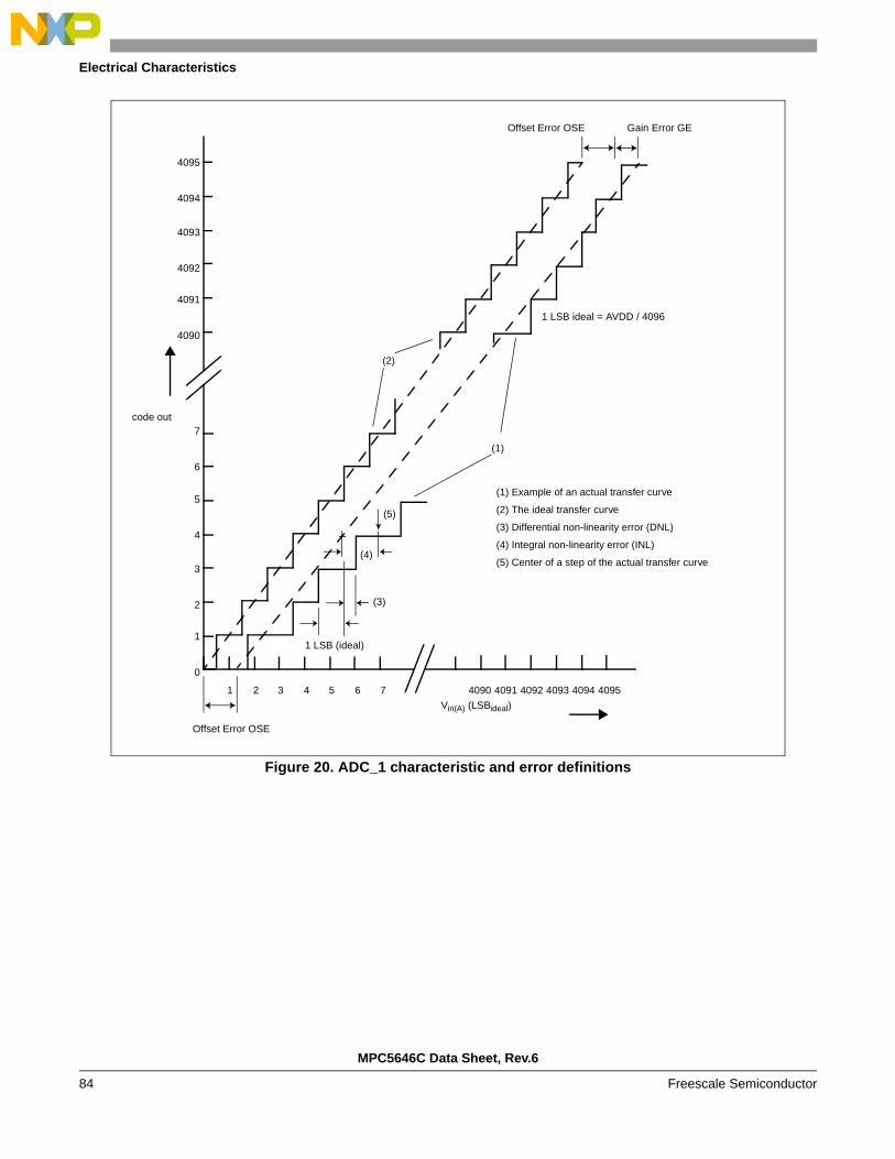
Electrical Characteristics
Figure 20. ADC_1 characteristic and error definitions
(2)
(1)
(3)
(4)
(5)
Offset Error OSE
Offset Error OSE
Gain Error GE
1 LSB (ideal)
Vin(A) (LSBideal)
(1) Example of an actual transfer curve
(2) The ideal transfer curve
(3) Differential non-linearity error (DNL)
(4) Integral non-linearity error (INL)
(5) Center of a step of the actual transfer curve
code out
4095
4094
4093
4092
4091
4090
5
4
3
2
1
0
7
6
1 2 3 4 5 6 7 4090 4091 4092 4093 4094 4095
1 LSB ideal = AVDD / 4096
MPC5646C Data Sheet, Rev.6
Freescale Semiconductor84

Electrical Characteristics
Table 43. Conversion characteristics (12-bit ADC_1)
Symbol C Parameter Conditions1Value
UnitMin Typ Max
VSS_ADC1 SR — Voltage on VSS_HV_ADC1 (ADC_1 reference) pin with respect to ground (VSS_HV)2
— 0.1 0.1 V
VDD_ADC13 SR — Voltage on
VDD_HV_ADC1 pin (ADC_1 reference) with respect to ground (VSS_HV)
— VDD_HV_A 0.1 VDD_HV_A + 0.1 V
VAINx3,4 SR — Analog input
voltage5— VSS_ADC1 0.1 VDD_ADC1 + 0.1 V
fADC1 SR — ADC_1 analog frequency
— 8 + 2% 32 + 2% MHz
tADC1_PU SR — ADC_1 power up delay
— 1.5 µs
tADC1_S CC T Sample time6
VDD=5.0 V— 440 ns
Sample time(6)
VDD=3.3 V— 530
tADC1_C CC P Conversion time7, 8
VDD=5.0 VfADC1 = 32 MHz 2
µs
Conversion time(7),
(6)
VDD =5.0 V
fADC 1= 30 MHz 2.1
Conversion time(7),
(6)
VDD=3.3 V
fADC 1= 20 MHz 3
Conversion time(7),
(6)
VDD =3.3 V
fADC1 = 15 MHz 3.01
CS CC D ADC_1 input sampling capacitance
— 5 pF
CP1 CC D ADC_1 input pin capacitance 1
— 3 pF
CP2 CC D ADC_1 input pin capacitance 2
— 1 pF
CP3 CC D ADC_1 input pin capacitance 3
— 1.5 pF
RSW1 CC D Internal resistance of analog source
— 1 k
MPC5646C Data Sheet, Rev.6
Freescale Semiconductor 85

Electrical Characteristics
RSW2 CC D Internal resistance of analog source
— 2 k
RAD CC D Internal resistance of analog source
— 0.3 k
IINJ SR — Input current Injection
Current injection on one ADC_1 input, different from the converted one
VDD = 3.3 V ± 10%
5 — 5 mA
VDD = 5.0 V ± 10%
5 — 5
INLP CC T Absolute Integral non-linearity-Precise channels
No overload 1 3 LSB
INLS CC T Absolute Integral non-linearity- Standard channels
No overload 1.5 5 LSB
DNL CC T Absolute Differential non-linearity
No overload 0.5 1 LSB
OFS CC T Absolute Offset error
— 2 LSB
GNE CC T Absolute Gain error — 2 LSB
TUEP9 CC P Total Unadjusted Error for precise channels, input only pins
Without current injection
6 6 LSB
T With current injection 8 8 LSB
TUES(9) CC T Total Unadjusted Error for standard channel
Without current injection
10 10 LSB
T With current injection 12 12 LSB
NOTES:1 VDD = 3.3 V ± 10% / 5.0 V ± 10%, TA = 40 to 125 °C, unless otherwise specified.2 Analog and digital VSS_HV must be common (to be tied together externally).3 PA3, PA7, PA10, PA11 and PE12 ADC_1 channels are coming from VDD_HV_B domain hence VDD_HV_ADC1 should be
within ±100 mV of VDD_HV_B when these channels are used for ADC_1.4 VDD_HV_ADC1 can operate at 5V condition while VDD_HV_B can operate at 3.3V provided that ADC_1 channels coming
from VDD_HV_B domain are limited in max swing as VDD_HV_B.5 VAINx may exceed VSS_ADC1 and VDD_ADC1 limits, remaining on absolute maximum ratings, but the results of the
conversion will be clamped respectively to 0x000 or 0xFFF.6 During the sample time the input capacitance CS can be charged/discharged by the external source. The internal
resistance of the analog source must allow the capacitance to reach its final voltage level within tADC1_S. After the end of the sample time tADC1_S, changes of the analog input voltage have no effect on the conversion result. Values for the sample clock tADC1_S depend on programming.
Table 43. Conversion characteristics (12-bit ADC_1) (continued)
Symbol C Parameter Conditions1Value
UnitMin Typ Max
MPC5646C Data Sheet, Rev.6
Freescale Semiconductor86

Electrical Characteristics
4.18 Fast Ethernet ControllerMII signals use CMOS signal levels compatible with devices operating at 3.3 V. Signals are not TTL compatible. They follow the CMOS electrical characteristics.
4.18.1 MII Receive Signal Timing (RXD[3:0], RX_DV, RX_ER, and RX_CLK)
The receiver functions correctly up to a RX_CLK maximum frequency of 25 MHz +1%. There is no minimum frequency requirement. In addition, the system clock frequency must exceed four times the RX_CLK frequency in 2:1 mode and two times the RX_CLK frequency in 1:1 mode.
Figure 21. MII receive signal timing diagram
4.18.2 MII Transmit Signal Timing (TXD[3:0], TX_EN, TX_ER, TX_CLK)
The transmitter functions correctly up to a TX_CLK maximum frequency of 25 MHz +1%. There is no minimum frequency requirement. In addition, the system clock frequency must exceed four times the TX_CLK frequency in 2:1 mode and two times the TX_CLK frequency in 1:1 mode.
7 Conversion time = Bit evaluation time + Sampling time + 1 Clock cycle delay.8 Refer to ADC conversion table for detailed calculations.9 Total Unadjusted Error: The maximum error that occurs without adjusting Offset and Gain errors. This error is a
combination of Offset, Gain and Integral Linearity errors.
Table 44. MII Receive Signal Timing
Spec Characteristic Min Max Unit
M1 RXD[3:0], RX_DV, RX_ER to RX_CLK setup
5 — ns
M2 RX_CLK to RXD[3:0], RX_DV, RX_ER hold
5 — ns
M3 RX_CLK pulse width high
35% 65% RX_CLK period
M4 RX_CLK pulse width low
35% 65% RX_CLK period
M1 M2
RX_CLK (input)
RXD[3:0] (inputs)RX_DVRX_ER
M3
M4
MPC5646C Data Sheet, Rev.6
Freescale Semiconductor 87

Electrical Characteristics
The transmit outputs (TXD[3:0], TX_EN, TX_ER) can be programmed to transition from either the rising or falling edge of TX_CLK, and the timing is the same in either case. This options allows the use of non-compliant MII PHYs.
Refer to the Fast Ethernet Controller (FEC) chapter of the MPC5646C Reference Manual for details of this option and how to enable it.
Figure 22. MII transmit signal timing diagram
4.18.3 MII Async Inputs Signal Timing (CRS and COL)
Table 45. MII transmit signal timing1
NOTES:1 Output pads configured with SRE = 0b11.
Spec Characteristic Min Max Unit
M5 TX_CLK to TXD[3:0], TX_EN, TX_ER invalid
5 — ns
M6 TX_CLK to TXD[3:0], TX_EN, TX_ER valid
— 25 ns
M7 TX_CLK pulse width high
35% 65% TX_CLK period
M8 TX_CLK pulse width low
35% 65% TX_CLK period
Table 46. MII Async Inputs Signal Timing1
NOTES:1 Output pads configured with SRE = 0b11.
Spec Characteristic Min Max Unit
M9 CRS, COL minimum pulse width
1.5 — TX_CLK period
M6
TX_CLK (input)
TXD[3:0] (outputs)TX_ENTX_ER
M5
M7
M8
MPC5646C Data Sheet, Rev.6
Freescale Semiconductor88

Electrical Characteristics
Figure 23. MII async inputs timing diagram
4.18.4 MII Serial Management Channel Timing (MDIO and MDC)
The FEC functions correctly with a maximum MDC frequency of 2.5 MHz.
Table 47. MII serial management channel timing1
NOTES:1 Output pads configured with SRE = 0b11.
Spec Characteristic Min Max Unit
M10 MDC falling edge to MDIO output invalid (minimum propagation delay)
0 — ns
M11 MDC falling edge to MDIO output valid (max prop delay)
— 25 ns
M12 MDIO (input) to MDC rising edge setup
28 — ns
M13 MDIO (input) to MDC rising edge hold
0 — ns
M14 MDC pulse width high
40% 60% MDC period
M15 MDC pulse width low 40% 60% MDC period
CRS, COL
M9
MPC5646C Data Sheet, Rev.6
Freescale Semiconductor 89

Electrical Characteristics
Figure 24. MII serial management channel timing diagram
M11
MDC (output)
MDIO (output)
M12M13
MDIO (input)
M10
M14 M15
MPC5646C Data Sheet, Rev.6
Freescale Semiconductor90

Electrical Characteristics
4.19 On-chip peripherals
4.19.1 Current consumption
Table 48. On-chip peripherals current consumption1
Symbol C Parameter ConditionsValue2
UnitTyp
IDD_HV_A(CAN) CC D CAN (FlexCAN) supply current on VDD_HV_A
500 Kbps
Total (static + dynamic) consumption:FlexCAN in loop-back mode XTAL@8 MHz used as CAN engine clock sourceMessage sending period is 580 µs
7.652 fperiph + 84.73 µA
125 Kbps
8.0743 fperiph + 26.757
IDD_HV_A(eMIOS) CC D eMIOS supply current on VDD_HV_A
Static consumption:eMIOS channel OFFGlobal prescaler enabled
28.7 fperiph
Dynamic consumption:It does not change varying the frequency (0.003 mA)
3
IDD_HV_A(SCI) CC D SCI (LINFlex) supply current on VDD_HV_A
Total (static + dynamic) consumption:LIN mode Baudrate: 20 Kbps
4.7804 fperiph + 30.946
IDD_HV_A(SPI) CC D SPI (DSPI) supply current on VDD_HV_A
Ballast static consumption (only clocked)
1
Ballast dynamic consumption (continuous communication):Baudrate: 2 MbitTransmission every 8 µsFrame: 16 bits
16.3 fperiph
IDD_HV_A(ADC) CC D ADC supply current on VDD_HV_A
VDD = 5.5 V
Ballast static consumption (no conversion)
0.0409 fperiph mA
VDD = 5.5 V
Ballast dynamic consumption (continuous conversion)
0.0049 fperiph
IDD_HV_ADC0 CC D ADC_0 supply current on VDD_HV_ADC0
VDD = 5.5 V
Analog static consumption (no conversion)
200 µA
Analog dynamic consumption(continuous conversion)
4 mA
MPC5646C Data Sheet, Rev.6
Freescale Semiconductor 91

Electrical Characteristics
IDD_HV_ADC1 CC D ADC_1 supply current on VDD_HV_ADC1
VDD = 5.5 V
Analog static consumption (no conversion)
300 fperiph µA
VDD = 5.5 V
Analog dynamic consumption (continuous conversion)
6 mA
IDD_HV(FLASH) CC D CFlash + DFlash supply current on VDD_HV_ADC
VDD = 5.5 V
— 13.25 mA
IDD_HV(PLL) CC D PLL supply current on VDD_HV
VDD = 5.5 V
— 0.0031 fperiph
NOTES:1 Operating conditions: TA = 25 °C, fperiph = 8 MHz to 120 MHz.2 fperiph is in absolute value.
Table 48. On-chip peripherals current consumption1
Symbol C Parameter ConditionsValue2
UnitTyp
MPC5646C Data Sheet, Rev.6
Freescale Semiconductor92

Electrical Characteristics
4.19.2 DSPI characteristics
Table 49. DSPI timing
Spec Characteristic Symbol UnitMin Max
1 DSPI Cycle Time tSCK Refer note1
— ns
— Internal delay between pad associated to SCK and pad associated to CSn in master mode for CSn1->0
tCSC — 115 ns
— Internal delay between pad associated to SCK and pad associated to CSn in master mode for CSn1->1
tASC 15 — ns
2 CS to SCK Delay2 tCSC 7 — ns
3 After SCK Delay3 tASC 15 — ns
4 SCK Duty Cycle tSDC 0.4 tSCK 0.6 tSCK ns
— Slave Setup Time(SS active to SCK setup time)
tSUSS 5 — ns
— Slave Hold Time(SS active to SCK hold time)
tHSS 10 — ns
5 Slave Access Time(SS active to SOUT valid)4
tA — 42 ns
6 Slave SOUT Disable Time(SS inactive to SOUT High-Z or invalid)
tDIS — 25 ns
7 CSx to PCSS time tPCSC 0 — ns
8 PCSS to PCSx time tPASC 0 — ns
MPC5646C Data Sheet, Rev.6
Freescale Semiconductor 93

Electrical Characteristics
9 Data Setup Time for InputsMaster (MTFE = 0)SlaveMaster (MTFE = 1, CPHA = 0)5
Master (MTFE = 1, CPHA = 1)
tSUI365
3636
————
nsnsnsns
10 Data Hold Time for InputsMaster (MTFE = 0)SlaveMaster (MTFE = 1, CPHA = 0)5
Master (MTFE = 1, CPHA = 1)
tHI0400
————
nsnsnsns
11 Data Valid (after SCK edge) Master (MTFE = 0)SlaveMaster (MTFE = 1, CPHA = 0)Master (MTFE = 1, CPHA = 1)
tSUO————
12371212
nsnsnsns
12 Data Hold Time for OutputsMaster (MTFE = 0)SlaveMaster (MTFE = 1, CPHA = 0)Master (MTFE = 1, CPHA = 1)
tHO06
9.507
08
————
nsnsnsns
NOTES:1 This value of this parameter is dependent upon the external device delays and the other parameters mentioned in
this table. 2 The maximum value is programmable in DSPI_CTARn [PSSCK] and DSPI_CTARn [CSSCK]. For MPC5646C, the
spec value of tCSC will be attained only if TDSPI x PSSCK x CSSCK > tCSC.3 The maximum value is programmable in DSPI_CTARn [PASC] and DSPI_CTARn [ASC]. For MPC5646C, the spec
value of tASC will be attained only if TDSPI x PASC x ASC > tASC.4 The parameter value is obtained from tSUSS and tSUO for slave.5 This number is calculated assuming the SMPL_PT bitfield in DSPI_MCR is set to 0b00.6 For DSPI1, the Data Hold Time for Outputs in Master (MTFE = 0) is 2 ns.7 For DSPI1, the Data Hold Time for Outputs in Master (MTFE = 1, CPHA = 0) is 2 n.8 For DSPI1, the Data Hold Time for Outputs in Master (MTFE = 1, CPHA = 1) is 2 ns.
Table 49. DSPI timing (continued)
Spec Characteristic Symbol UnitMin Max
MPC5646C Data Sheet, Rev.6
Freescale Semiconductor94

Electrical Characteristics
Figure 25. DSPI classic SPI timing–master, CPHA = 0
Figure 26. DSPI classic SPI timing–master, CPHA = 1
Data Last DataFirst Data
First Data Data Last Data
SIN
SOUT
CSx
SCK Output
4
9
12
1
11
10
4
SCK Output
(CPOL = 0)
(CPOL = 1)
32
Note: Numbers shown reference Table 49.
Data Last DataFirst DataSIN
SOUT
12 11
10
Last DataDataFirst Data
SCK Output
SCK Output
CSx
9
(CPOL = 0)
(CPOL = 1)
Note: Numbers shown reference Table 49.
MPC5646C Data Sheet, Rev.6
Freescale Semiconductor 95

Electrical Characteristics
Figure 27. DSPI classic SPI timing–slave, CPHA = 0
Last DataFirst Data
3
4
1
Data
Data
SIN
SOUT
SS
4
5 6
9
11
10
12
SCK Input
First Data Last Data
SCK Input
2
(CPOL = 0)
(CPOL = 1)
Note: Numbers shown reference Table 49.
MPC5646C Data Sheet, Rev.6
Freescale Semiconductor96

Electrical Characteristics
Figure 28. DSPI classic SPI timing–slave, CPHA = 1
5 6
9
12
11
10
Last Data
Last DataSIN
SOUT
SS
First Data
First Data
Data
Data
SCK Input
SCK Input
(CPOL = 0)
(CPOL = 1)
Note: Numbers shown reference Table 49.
MPC5646C Data Sheet, Rev.6
Freescale Semiconductor 97

Electrical Characteristics
Figure 29. DSPI modified transfer format timing–master, CPHA = 0
CSx
3
14
10
4
9
12 11
SCK Output
SCK Output
SIN
SOUT
First Data Data Last Data
First Data Data Last Data
2
(CPOL = 0)
(CPOL = 1)
Note: Numbers shown reference Table 49.
MPC5646C Data Sheet, Rev.6
Freescale Semiconductor98

Electrical Characteristics
Figure 30. DSPI modified transfer format timing–master, CPHA = 1
CSx
109
12 11
SCK Output
SCK Output
SIN
SOUT
First Data Data Last Data
First Data Data Last Data
(CPOL = 0)
(CPOL = 1)
Note: Numbers shown reference Table 49.
MPC5646C Data Sheet, Rev.6
Freescale Semiconductor 99

Electrical Characteristics
Figure 31. DSPI modified transfer format timing–slave, CPHA = 0
Figure 32. DSPI modified transfer format timing–slave, CPHA = 1
Last DataFirst Data
3
4
1
Data
Data
SIN
SOUT
SS
4
5 6
9
11
10
SCK Input
First Data Last Data
SCK Input
2
(CPOL = 0)
(CPOL = 1)
12
Note: Numbers shown reference Table 49.
5 6
9
12
11
10
Last Data
Last DataSIN
SOUT
SS
First Data
First Data
Data
Data
SCK Input
SCK Input
(CPOL = 0)
(CPOL = 1)
Note: Numbers shown reference Table 49.
MPC5646C Data Sheet, Rev.6
Freescale Semiconductor100

Electrical Characteristics
Figure 33. DSPI PCS strobe (PCSS) timing
4.19.3 Nexus characteristics
Table 50. Nexus debug port timing1
NOTES:1 JTAG specifications in this table apply when used for debug functionality. All Nexus timing relative to MCKO is
measured from 50% of MCKO and 50% of the respective signal. Nexus timing specified at VDDE = 4.0 – 5.5 V, TA = TL to TH, and CL = 30 pF with SRC = 0b11.
Spec Characteristic Symbol Min Max Unit
1 MCKO Cycle Time2
2 MCKO can run up to 1/2 of full system frequency. It can also run at system frequency when it is <60 MHz.
tMCYC 16.3 — ns
2 MCKO Duty Cycle tMDC 40 60 %
3 MCKO Low to MDO, MSEO, EVTO Data Valid3
3 MDO, MSEO, and EVTO data is held valid until next MCKO low cycle.
tMDOV –0.1 0.25 tMCYC
4 EVTI Pulse Width tEVTIPW 4.0 — tTCYC
5 EVTO Pulse Width
tEVTOPW 1 tMCYC
6 TCK Cycle Time4
4 The system clock frequency needs to be three times faster than the TCK frequency.
tTCYC 40 — ns
7 TCK Duty Cycle tTDC 40 60 %
8 TDI, TMS Data Setup Time
tNTDIS, tNTMSS 8 — ns
9 TDI, TMS Data Hold Time
tNTDIH, tNTMSH 5 — ns
10 TCK Low to TDO Data Valid
tJOV 0 25 ns
CSx
7 8
PCSS
Note: Numbers shown reference Table 49.
MPC5646C Data Sheet, Rev.6
Freescale Semiconductor 101
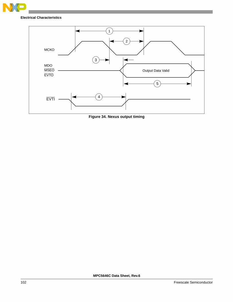
Electrical Characteristics
Figure 34. Nexus output timing
1
2
MCKO
MDOMSEOEVTO
Output Data Valid
3
EVTI4
5
MPC5646C Data Sheet, Rev.6
Freescale Semiconductor102

Electrical Characteristics
Figure 35. Nexus TDI, TMS, TDO timing
4.19.4 JTAG characteristics
Table 51. JTAG characteristics
No. Symbol C ParameterValue
UnitMin Typ Max
1 tJCYC CC D TCK cycle time 64 — — ns
2 tTDIS CC D TDI setup time 10 — — ns
3 tTDIH CC D TDI hold time 5 — — ns
4 tTMSS CC D TMS setup time 10 — — ns
5 tTMSH CC D TMS hold time 5 — — ns
TDO
8
9
TMS, TDI
10
TCK
6
7
MPC5646C Data Sheet, Rev.6
Freescale Semiconductor 103

Electrical Characteristics
Figure 36. Timing diagram - JTAG boundary scan
6 tTDOV CC D TCK low to TDO valid — — 33 ns
7 tTDOI CC D TCK low to TDO invalid 6 — — ns
— tTDC CC D TCK Duty Cycle 40 — 60 %
— tTCKRISE CC D TCK Rise and Fall Times — — 3 ns
Table 51. JTAG characteristics (continued)
No. Symbol C ParameterValue
UnitMin Typ Max
INPUT DATA VALID
OUTPUT DATA VALID
DATA INPUTS
DATA OUTPUTS
DATA OUTPUTS
TCK
Note: Numbers shown reference Table 51.
3/52/4
7
6
MPC5646C Data Sheet, Rev.6
Freescale Semiconductor104

Package characteristics
5 Package characteristics
5.1 Package mechanical data
5.1.1 176 LQFP package mechanical drawing
MPC5646C Data Sheet, Rev.6
Freescale Semiconductor 105

Package characteristics
Figure 37. 176 LQFP mechanical drawing (Part 1 of 3)
MPC5646C Data Sheet, Rev.6
Freescale Semiconductor106
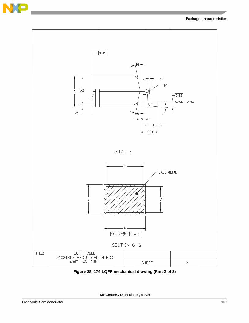
Package characteristics
Figure 38. 176 LQFP mechanical drawing (Part 2 of 3)
MPC5646C Data Sheet, Rev.6
Freescale Semiconductor 107

Package characteristics
Figure 39. 176 LQFP mechanical drawing (Part 3 of 3)
5.1.2 208 LQFP package mechanical drawing
E
E
MPC5646C Data Sheet, Rev.6
Freescale Semiconductor108

Package characteristics
Figure 40. 208 LQFP mechanical drawing (Part 1 of 3)
MPC5646C Data Sheet, Rev.6
Freescale Semiconductor 109

Package characteristics
Figure 41. 208 LQFP mechanical drawing (Part 2 of 3)
MPC5646C Data Sheet, Rev.6
Freescale Semiconductor110

Package characteristics
Figure 42. 208 LQFP mechanical drawing (Part 3 of 3)
MPC5646C Data Sheet, Rev.6
Freescale Semiconductor 111

Package characteristics
MPC5646C Data Sheet, Rev.6
Freescale Semiconductor112

Package characteristics
5.1.3 256 MAPBGA package mechanical drawing
Figure 43. 256 MAPBGA mechanical drawing (Part 1 of 2)
MPC5646C Data Sheet, Rev.6
Freescale Semiconductor 113

Package characteristics
Figure 44. 256 MAPBGA mechanical drawing (Part 2 of 2)
MPC5646C Data Sheet, Rev.6
Freescale Semiconductor114

Ordering information
6 Ordering information
Figure 45. Orderable parts
Qualification Status
Power Architecture
Automotive Platform
Core Version
Flash Size (core dependent)
Product
Optional fields
M PC 56 C F0 LLExample code: 4 6
Temperature spec.
Package Code
Qualification StatusM = MC statusS = Auto qualifiedP = PC status
PC = Power Architecture
Automotive Platform56 = Power Architecture in 90 nm
Core Version4 = e200z4d core version (highest core version in the case of multiple cores)
Flash Memory Size4 = 1.5 MB5 = 2 MB6 = 3 MB
Product VersionB = BodyC = Gateway
Optional fieldsC = CSE module availableBlank = none of these options available
Fab and mask version indicatorF = ATMC0 = First version of the mask
Temperature spec.C = –40 °C to 85 °CV = –40 °C to 105 °CM = –40 °C to 125 °C
R = Tape & Reel (blank if Tray)
R
Package CodeLU = 176 LQFPLT = 208 LQFPMJ = 256 MAPBGA
CPU Frequency1 = e200z4d operates up to 120 MHz8 = e200z4d operates up to 80 MHz
Shipping MethodR = Tape and reelBlank = Tray
1
CPU Frequency
Fab and mask indicator
MB
Note: Not all options are available on all devices. Refer to Table 1, which shows the orderable part numbers forMPC564xx.
MPC5646C Data Sheet, Rev.6
Freescale Semiconductor 115

Revision history
7 Revision historyTable 52 summarizes revisions to this document.
Table 52. Revision history
Revision Date Changes
1 15 April 2010 Initial Release
2 17 August 2010 • Editing and formatting updates throughout the document. • Updated Voltage regulator capacitance connection figure. • Added a new sub-section “VDD_BV Options” • Program and erase specifications:
-Updated Tdwprogram TYP to 22 us-Updated T128Kpperase Max to 5000 ms-Added tESUS parameter
• Added 208 MAPBGA thermal characteristics • Added recommendation in the Voltage regulator electrical characteristics section. • Added Crystal description table in Fast external crystal oscillator (4 to 140 MHz)
electrical characteristics section and corrected the cross-reference to the same. • Added new sections - Pad types, System pins and functional ports • Updated TYP numbers in the Flash program and erase specifications table • Added a new table: Program and erase specifications (Data Flash) • Flash read access timing table: Added Data flash memory numbers • Flash power supply DC electrical characteristics table: Updated IDFREAD and
IDFMOD values for Data flash, Removed IDFLPW parameter • Updated feature list. • MPC5646C 3M family comparison table: Updated ADC channels and added ADC
footnotes. • MPC5646C 3M block diagram: Updated ADC channels and added legends. • MPC5646C 3M series block summary: Added new blocks. • Functional Port Pin Descriptions table: Added OSC32k_XTAL and
OSC32k_EXTAL function at PB8 and PB9 port pins. • Electrical Characteristics: Replaced VSS with VSS_HV throughout the section. • Absolute maximum ratings, Recommended operating conditions (3.3 V) and
Recommended operating conditions (5.0 V) tables: VRC_CTRL min is updated to "0".
• Recommended operating conditions (3.3 V) and Recommended operating conditions (5.0 V) tables: Clarified VIN parameter, clarified footnote 2 in both tables.
• LQFP thermal characteristics section: Updated numbers for LQFP packages. • Low voltage power domain electrical characteristics table: Clarified footnotes
based upon review comments. • Code flash memory—Program and erase specifications: Updated tESRT to 20 ms. • ADC electrical characteristics section: Replace ADC0 with ADC_0 and ADC1 with
ADC_1 throughout the document. • DSPI characteristics section: Replaced PCSx with CSx in all figures and tables.
MPC5646C Data Sheet, Rev.6
Freescale Semiconductor116

Revision history
3 28 April 2011 • Replaced VIL min from –0.4 V to –0.3 V in the following tables: - I/O input DC electrical characteristics- Reset electrical characteristics- Fast external crystal oscillator (4 to 40 MHz) electrical characteristics
• Updated Crystal oscillator and resonator connection scheme figure • Specified NPN transistor as the recommended BCP68 transistor throughout the
document • Code and Data flash memory—Program and erase specifications tables:
Renamed the parameter tESUS to Teslat • Revised the footnotes in the “Functional port pin descriptions” table. • In the “System pin descriptions” table, added a footnote to the A pads regarding
not using IBE.For ports PB[12–15], changed ANX to ADC0_X.
• Revised the presentation of the ADC functions on the following ports:PB[4–7]
PD[0–11] • ADC conversion characteristics (10-bit ADC_0) table and Conversion
characteristics (12-bit ADC_1) table- Updated footnote 5 and 7 respectively for the definition of the conversion time.
• Data flash memory—Program and erase specifications: Updated Twprogram to 500 µs and T16Kpperase to 500 µs. Corrected Teslat classification from “C” to “D”.
• Code flash memory—Program and erase specifications: Corrected Teslat classification from “C” to “D”.
• Flash Start-up time/Switch-off time: Changed TFLARSTEXIT classification from “C” to “D”.
• Functional port pin description: Added a footnote at the PB [9] port pin. • Absolute maximum ratings table: Added footnote 1. • Low voltage power domain electrical characteristics table: Updated IDDHALT,
IDDSTOP, IDDSTBY3, IDDSTDBY2, IDDSTDBY1. • Slow external crystal oscillator (32 kHz) electrical characteristics table: Updated
gmSXOSC, VSXOSC, ISXOSCBIAS and ISXOSC. • FMPLL electrical characteristics table: Updated tLTJIT. • Fast internal RC oscillator (16 MHz) electrical characteristics table: Updated
TFIRCSU and IFIRCPWD. • MII serial management channel timing table: Updated M12 • JTAG characteristics table: Updated tTDOV. • Low voltage monitor electrical characteristics table: Updated VLVDHV3H,
VLVDHV3L, VLVDHV5H, VLVDHV5L. • DSPI electricals table: Updated spec 1, 5, 6. Updated footnote 2 and 3. Added tCSC, tASC, tSUSS, tHSS.
• IO consumption table: Updated all parameter values. • DSPI electricals: Updated tCSC max to 115 ns. • Low voltage power domain electrical characteristics table: Added footnote 9. • ADC electrical characteristics: Added 2 notes above 10-bit and 12-bit conversion
tables.
Table 52. Revision history (continued)
Revision Date Changes
MPC5646C Data Sheet, Rev.6
Freescale Semiconductor 117
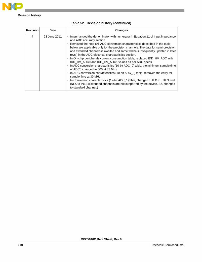
Revision history
4 23 June 2011 • Interchanged the denominator with numerator in Equation 11 of Input impedance and ADC accuracy section
• Removed the note (All ADC conversion characteristics described in the table below are applicable only for the precision channels. The data for semi-precision and extended channels is awaited and same will be subsequently updated in later revs.) in the ADC electrical characteristics section.
• In On-chip peripherals current consumption table, replaced IDD_HV_ADC with IDD_HV_ADC0 and IDD_HV_ADC1 values as per ADC specs
• In ADC conversion characteristics (10-bit ADC_0) table, the minimum sample time of ADC0 changed to 500 at 32 MHz
• In ADC conversion characteristics (10-bit ADC_0) table, removed the entry for sample time at 30 MHz
• In Conversion characteristics (12-bit ADC_1)table, changed TUEX to TUES and INLX to INLS (Extended channels are not supported by the device. So, changed to standard channel.)
Table 52. Revision history (continued)
Revision Date Changes
MPC5646C Data Sheet, Rev.6
Freescale Semiconductor118
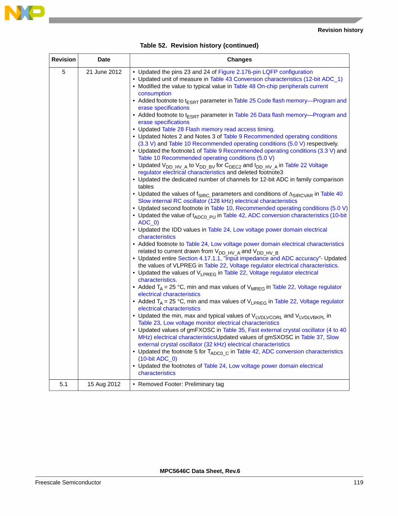
Revision history
5 21 June 2012 • Updated the pins 23 and 24 of Figure 2.176-pin LQFP configuration • Updated unit of measure in Table 43 Conversion characteristics (12-bit ADC_1) • Modified the value to typical value in Table 48 On-chip peripherals current
consumption • Added footnote to tESRT parameter in Table 25 Code flash memory—Program and
erase specifications • Added footnote to tESRT parameter in Table 26 Data flash memory—Program and
erase specifications • Updated Table 28 Flash memory read access timing. • Updated Notes 2 and Notes 3 of Table 9 Recommended operating conditions
(3.3 V) and Table 10 Recommended operating conditions (5.0 V) respectively. • Updated the footnote1 of Table 9 Recommended operating conditions (3.3 V) and
Table 10 Recommended operating conditions (5.0 V) • Updated VDD_HV_A to VDD_BV for CDEC2 and IDD_HV_A in Table 22 Voltage
regulator electrical characteristics and deleted footnote3 • Updated the dedicated number of channels for 12-bit ADC in family comparison
tables • Updated the values of fSIRC, parameters and conditions of SIRCVAR in Table 40
Slow internal RC oscillator (128 kHz) electrical characteristics • Updated second footnote in Table 10, Recommended operating conditions (5.0 V) • Updated the value of tADC0_PU in Table 42, ADC conversion characteristics (10-bit
ADC_0) • Updated the IDD values in Table 24, Low voltage power domain electrical
characteristics • Added footnote to Table 24, Low voltage power domain electrical characteristics
related to current drawn from VDD_HV_A and VDD_HV_B • Updated entire Section 4.17.1.1, ”Input impedance and ADC accuracy”- Updated
the values of VLPREG in Table 22, Voltage regulator electrical characteristics. • Updated the values of VLPREG in Table 22, Voltage regulator electrical
characteristics. • Added TA = 25 °C, min and max values of VMREG in Table 22, Voltage regulator
electrical characteristics • Added TA = 25 °C, min and max values of VLPREG in Table 22, Voltage regulator
electrical characteristics • Updated the min, max and typical values of VLVDLVCORL and VLVDLVBKPL in
Table 23, Low voltage monitor electrical characteristics • Updated values of gmFXOSC in Table 35, Fast external crystal oscillator (4 to 40
MHz) electrical characteristicsUpdated values of gmSXOSC in Table 37, Slow external crystal oscillator (32 kHz) electrical characteristics
• Updated the footnote 5 for TADC0_C in Table 42, ADC conversion characteristics (10-bit ADC_0)
• Updated the footnotes of Table 24, Low voltage power domain electrical characteristics
5.1 15 Aug 2012 • Removed Footer: Preliminary tag
Table 52. Revision history (continued)
Revision Date Changes
MPC5646C Data Sheet, Rev.6
Freescale Semiconductor 119

Revision history
NOTEThis revision history uses clickable cross-references for ease of navigation. The numbers and titles in each cross-reference are relative to the latest published release.
6 12 Feb 2014 • Removed occurrences of 208BGA from Table 3 System pin descriptions. • Added PM[3] and PM[4] in the figure note 1 of Figure 4, 256-pin BGA
configuration. • Added a table note in Table 19 I/O supplies. • Updated Figure 8, Voltage regulator capacitance connection and added a note in
this figure. • Removed max values of VLPREG and VMREG, changed min value of VLPREG to 1.21
V, and updated VMREG and VLPREG after trimming values in Table 22 Voltage regulator electrical characteristics.
• Updated 1st footnote and updated max values for IDDRUN, IDDHALT, IDDSTOP, IDDSTDBY3, IDDSTDBY2, IDDSTDBY1 and removed values at 85oC and 105oC in Table 24 Low voltage power domain electrical characteristics.
• Added a footnote below Table 28 Flash memory read access timing. • Updated the formula in Eq. 11 in Section 4.17.1.1, ”Input impedance and ADC
accuracy. • Added Figure 17, Input equivalent circuit (extended channels). • Updated tADC0_PU value to 1.5 as max and added footnote for IINJ in Table 42 ADC
conversion characteristics (10-bit ADC_0). • Added Category column in Table 43 Conversion characteristics (12-bit ADC_1). • Added the IDD_HV_ADC0 values in Table 48 On-chip peripherals current
consumption. • Added a note in Figure 45, Orderable parts.
Table 52. Revision history (continued)
Revision Date Changes
MPC5646C Data Sheet, Rev.6
Freescale Semiconductor120

Abbreviations
Appendix A AbbreviationsTable 53 lists abbreviations used but not defined elsewhere in this document.
Table 53. Abbreviations
Abbreviation Meaning
CS Chip select
EVTO Event out
MCKO Message clock out
MDO Message data out
MSEO Message start/end out
MTFE Modified timing format enable
SCK Serial communications clock
SOUT Serial data out
TBD To be defined
TCK Test clock input
TDI Test data input
TDO Test data output
TMS Test mode select
MPC5646C Data Sheet, Rev.6
Freescale Semiconductor 121

How to Reach Us:
Home Page:www.freescale.com
Web Support:http://www.freescale.com/support
MPC5646CRev.602/2014
Information in this document is provided solely to enable system and software implementers to use Freescale Semiconductor products. There are no express or implied copyright licenses granted hereunder to design or fabricate any integrated circuits or integrated circuits based on the information in this document.
Freescale reserves the right to make changes without further
notice to any products herein. Freescale makes no warranty,
representation, or guarantee regarding the suitability of its
products for any particular purpose, nor does Freescale assume
any liability arising out of the application or use of any product or
circuit, and specifically disclaims any and all liability, including
without limitation consequential or incidental damages. “Typical”
parameters that may be provided in Freescale data sheets and/or
specifications can and do vary in different applications, and actual
performance may vary over time. All operating parameters,
including “typicals,” must be validated for each customer
application by customer’s technical experts. Freescale does not
convey any license under its patent rights nor the rights of others.
Freescale sells products pursuant to standard terms and
conditions of sale, which can be found at the following address:
http://www.reg.net/v2/webservices/Freescale/Docs/TermsandCo
nditions.html.
Freescale, the Freescale logo, is trademark of Freescale Semiconductor, Inc. All other product or service names are the property of their respective owners. The Power Architecture and Power.org word marks and the Power and Power.org logos and related marks are trademarks and service marks licensed by Power.org. © 2009-2014 Freescale Semiconductor, Inc.