Embed Size (px)
Citation preview
Frequency-selective plasmonic wave propagation through the overmodedwaveguide with photonic-band-gap slab arrays
Young-Min Shina)
Department of Physics, Northern Illinois University, Dekalb, Illinois 60115, USA and Accelerator PhysicsCenter (APC), Fermi National Accelerator Laboratory (FNAL), Batavia, Illinois 60510, USA
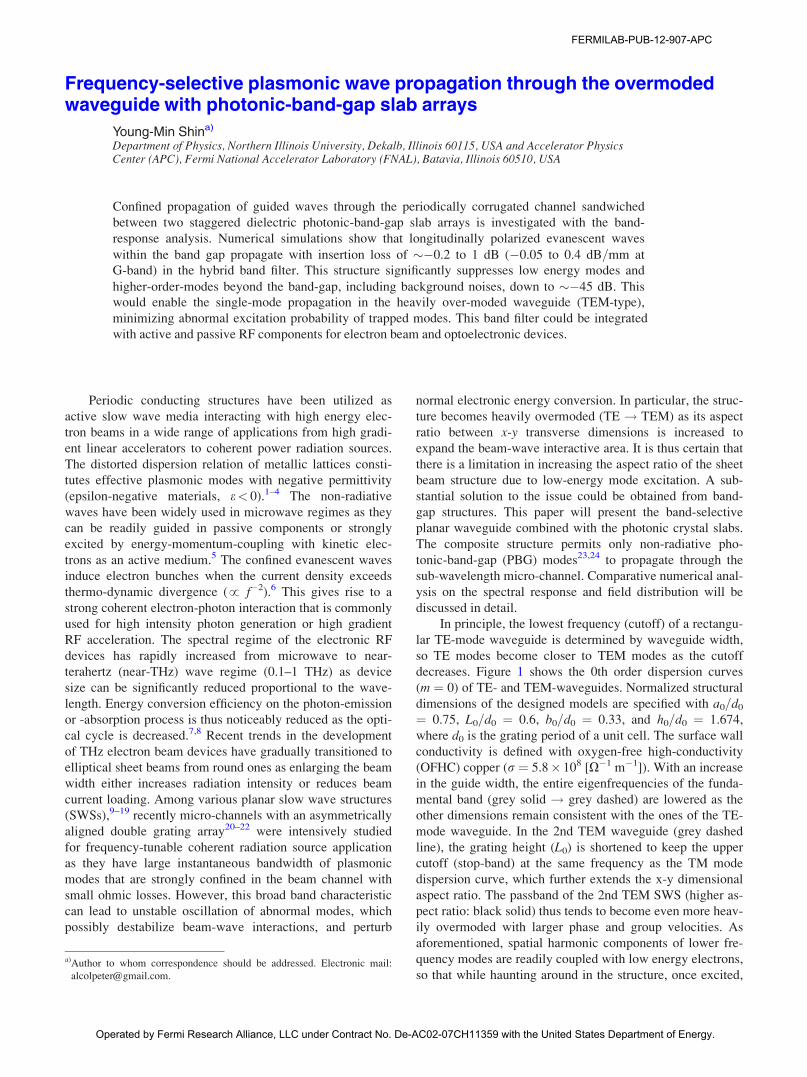
Confined propagation of guided waves through the periodically corrugated channel sandwiched
between two staggered dielectric photonic-band-gap slab arrays is investigated with the band-
response analysis. Numerical simulations show that longitudinally polarized evanescent waves
within the band gap propagate with insertion loss of ��0.2 to 1 dB (�0.05 to 0.4 dB=mm at
G-band) in the hybrid band filter. This structure significantly suppresses low energy modes and
higher-order-modes beyond the band-gap, including background noises, down to ��45 dB. This
would enable the single-mode propagation in the heavily over-moded waveguide (TEM-type),
minimizing abnormal excitation probability of trapped modes. This band filter could be integrated
with active and passive RF components for electron beam and optoelectronic devices.
Periodic conducting structures have been utilized as
active slow wave media interacting with high energy elec-
tron beams in a wide range of applications from high gradi-
ent linear accelerators to coherent power radiation sources.
The distorted dispersion relation of metallic lattices consti-
tutes effective plasmonic modes with negative permittivity
(epsilon-negative materials, e< 0).1–4 The non-radiative
waves have been widely used in microwave regimes as they
can be readily guided in passive components or strongly
excited by energy-momentum-coupling with kinetic elec-
trons as an active medium.5 The confined evanescent waves
induce electron bunches when the current density exceeds
thermo-dynamic divergence (! f�2).6 This gives rise to a
strong coherent electron-photon interaction that is commonly
used for high intensity photon generation or high gradient
RF acceleration. The spectral regime of the electronic RF
devices has rapidly increased from microwave to near-
terahertz (near-THz) wave regime (0.1–1 THz) as device
size can be significantly reduced proportional to the wave-
length. Energy conversion efficiency on the photon-emission
or -absorption process is thus noticeably reduced as the opti-
cal cycle is decreased.7,8 Recent trends in the development
of THz electron beam devices have gradually transitioned to
elliptical sheet beams from round ones as enlarging the beam
width either increases radiation intensity or reduces beam
current loading. Among various planar slow wave structures
(SWSs),9–19 recently micro-channels with an asymmetrically
aligned double grating array20–22 were intensively studied
for frequency-tunable coherent radiation source application
as they have large instantaneous bandwidth of plasmonic
modes that are strongly confined in the beam channel with
small ohmic losses. However, this broad band characteristic
can lead to unstable oscillation of abnormal modes, which
possibly destabilize beam-wave interactions, and perturb
normal electronic energy conversion. In particular, the struc-
ture becomes heavily overmoded (TE ! TEM) as its aspect
ratio between x-y transverse dimensions is increased to
expand the beam-wave interactive area. It is thus certain that
there is a limitation in increasing the aspect ratio of the sheet
beam structure due to low-energy mode excitation. A sub-
stantial solution to the issue could be obtained from band-
gap structures. This paper will present the band-selective
planar waveguide combined with the photonic crystal slabs.
The composite structure permits only non-radiative pho-
tonic-band-gap (PBG) modes23,24 to propagate through the
sub-wavelength micro-channel. Comparative numerical anal-
ysis on the spectral response and field distribution will be
discussed in detail.
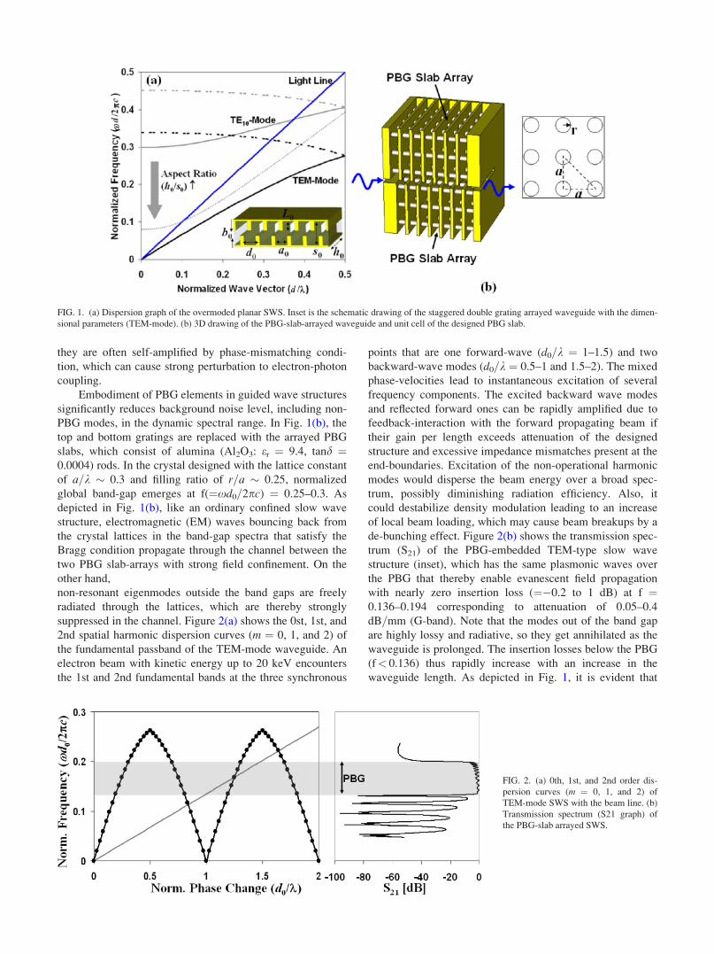
In principle, the lowest frequency (cutoff) of a rectangu-
lar TE-mode waveguide is determined by waveguide width,
so TE modes become closer to TEM modes as the cutoff
decreases. Figure 1 shows the 0th order dispersion curves
(m ¼ 0) of TE- and TEM-waveguides. Normalized structural
dimensions of the designed models are specified with a0=d0
¼ 0.75, L0=d0 ¼ 0.6, b0=d0 ¼ 0.33, and h0=d0 ¼ 1.674,
where d0 is the grating period of a unit cell. The surface wall
conductivity is defined with oxygen-free high-conductivity
(OFHC) copper (r ¼ 5.8� 108 [X�1 m�1]). With an increase
in the guide width, the entire eigenfrequencies of the funda-
mental band (grey solid ! grey dashed) are lowered as the
other dimensions remain consistent with the ones of the TE-
mode waveguide. In the 2nd TEM waveguide (grey dashed
line), the grating height (L0) is shortened to keep the upper
cutoff (stop-band) at the same frequency as the TM mode
dispersion curve, which further extends the x-y dimensional
aspect ratio. The passband of the 2nd TEM SWS (higher as-
pect ratio: black solid) thus tends to become even more heav-
ily overmoded with larger phase and group velocities. As
aforementioned, spatial harmonic components of lower fre-
quency modes are readily coupled with low energy electrons,
so that while haunting around in the structure, once excited,
a)Author to whom correspondence should be addressed. Electronic mail:
FERMILAB-PUB-12-907-APC
Operated by Fermi Research Alliance, LLC under Contract No. De-AC02-07CH11359 with the United States Department of Energy.
they are often self-amplified by phase-mismatching condi-
tion, which can cause strong perturbation to electron-photon
coupling.
Embodiment of PBG elements in guided wave structures
significantly reduces background noise level, including non-
PBG modes, in the dynamic spectral range. In Fig. 1(b), the
top and bottom gratings are replaced with the arrayed PBG
slabs, which consist of alumina (Al2O3: er ¼ 9.4, tand ¼0.0004) rods. In the crystal designed with the lattice constant
of a=k � 0.3 and filling ratio of r=a � 0.25, normalized
global band-gap emerges at f(¼xd0=2pc) ¼ 0.25–0.3. As
depicted in Fig. 1(b), like an ordinary confined slow wave
structure, electromagnetic (EM) waves bouncing back from
the crystal lattices in the band-gap spectra that satisfy the
Bragg condition propagate through the channel between the
two PBG slab-arrays with strong field confinement. On the
other hand,
non-resonant eigenmodes outside the band gaps are freely
radiated through the lattices, which are thereby strongly
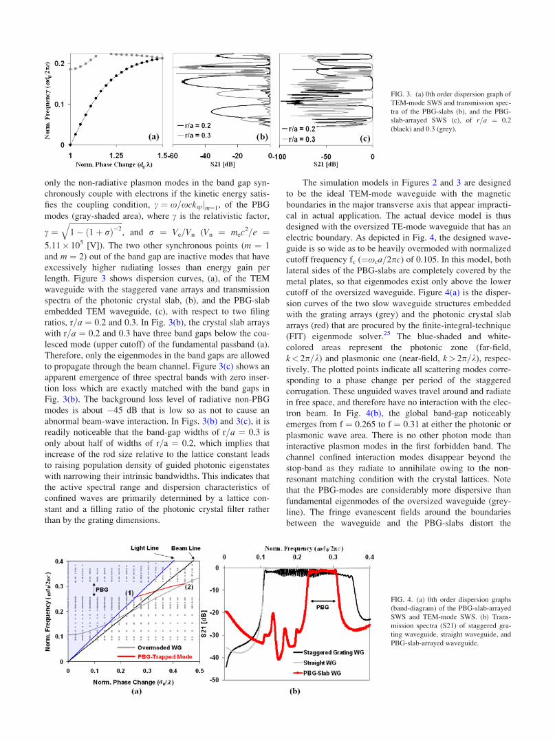
suppressed in the channel. Figure 2(a) shows the 0st, 1st, and
2nd spatial harmonic dispersion curves (m ¼ 0, 1, and 2) of
the fundamental passband of the TEM-mode waveguide. An
electron beam with kinetic energy up to 20 keV encounters
the 1st and 2nd fundamental bands at the three synchronous
points that are one forward-wave (d0=k ¼ 1–1.5) and two
backward-wave modes (d0=k ¼ 0.5–1 and 1.5–2). The mixed
phase-velocities lead to instantaneous excitation of several
frequency components. The excited backward wave modes
and reflected forward ones can be rapidly amplified due to
feedback-interaction with the forward propagating beam if
their gain per length exceeds attenuation of the designed
structure and excessive impedance mismatches present at the
end-boundaries. Excitation of the non-operational harmonic
modes would disperse the beam energy over a broad spec-
trum, possibly diminishing radiation efficiency. Also, it
could destabilize density modulation leading to an increase
of local beam loading, which may cause beam breakups by a
de-bunching effect. Figure 2(b) shows the transmission spec-
trum (S21) of the PBG-embedded TEM-type slow wave
structure (inset), which has the same plasmonic waves over
the PBG that thereby enable evanescent field propagation
with nearly zero insertion loss (¼�0.2 to 1 dB) at f ¼0.136–0.194 corresponding to attenuation of 0.05–0.4
dB=mm (G-band). Note that the modes out of the band gap
are highly lossy and radiative, so they get annihilated as the
waveguide is prolonged. The insertion losses below the PBG
(f< 0.136) thus rapidly increase with an increase in the
waveguide length. As depicted in Fig. 1, it is evident that
FIG. 1. (a) Dispersion graph of the overmoded planar SWS. Inset is the schematic drawing of the staggered double grating arrayed waveguide with the dimen-
sional parameters (TEM-mode). (b) 3D drawing of the PBG-slab-arrayed waveguide and unit cell of the designed PBG slab.
FIG. 2. (a) 0th, 1st, and 2nd order dis-
persion curves (m ¼ 0, 1, and 2) of
TEM-mode SWS with the beam line. (b)
Transmission spectrum (S21 graph) of
the PBG-slab arrayed SWS.
only the non-radiative plasmon modes in the band gap syn-
chronously couple with electrons if the kinetic energy satis-
fies the coupling condition, c ¼ x=xckspjm¼1, of the PBG
modes (gray-shaded area), where c is the relativistic factor,
c ¼ffiffiffiffiffiffiffiffiffiffiffiffiffiffiffiffiffiffiffiffiffiffiffiffiffiffiffiffi1� ð1þ rÞ�2
q, and r ¼ Ve=Vn (Vn ¼ mec
2=e ¼5.11� 105 [V]). The two other synchronous points (m ¼ 1
and m ¼ 2) out of the band gap are inactive modes that have
excessively higher radiating losses than energy gain per
length. Figure 3 shows dispersion curves, (a), of the TEM
waveguide with the staggered vane arrays and transmission
spectra of the photonic crystal slab, (b), and the PBG-slab
embedded TEM waveguide, (c), with respect to two filing
ratios, r=a ¼ 0.2 and 0.3. In Fig. 3(b), the crystal slab arrays
with r=a ¼ 0.2 and 0.3 have three band gaps below the coa-
lesced mode (upper cutoff) of the fundamental passband (a).
Therefore, only the eigenmodes in the band gaps are allowed
to propagate through the beam channel. Figure 3(c) shows an
apparent emergence of three spectral bands with zero inser-
tion loss which are exactly matched with the band gaps in
Fig. 3(b). The background loss level of radiative non-PBG
modes is about �45 dB that is low so as not to cause an
abnormal beam-wave interaction. In Figs. 3(b) and 3(c), it is
readily noticeable that the band-gap widths of r=a ¼ 0.3 is
only about half of widths of r=a ¼ 0.2, which implies that
increase of the rod size relative to the lattice constant leads
to raising population density of guided photonic eigenstates
with narrowing their intrinsic bandwidths. This indicates that
the active spectral range and dispersion characteristics of
confined waves are primarily determined by a lattice con-
stant and a filling ratio of the photonic crystal filter rather
than by the grating dimensions.
The simulation models in Figures 2 and 3 are designed
to be the ideal TEM-mode waveguide with the magnetic
boundaries in the major transverse axis that appear impracti-
cal in actual application. The actual device model is thus
designed with the oversized TE-mode waveguide that has an
electric boundary. As depicted in Fig. 4, the designed wave-
guide is so wide as to be heavily overmoded with normalized
cutoff frequency fc (¼xca=2pc) of 0.105. In this model, both
lateral sides of the PBG-slabs are completely covered by the
metal plates, so that eigenmodes exist only above the lower
cutoff of the oversized waveguide. Figure 4(a) is the disper-
sion curves of the two slow waveguide structures embedded
with the grating arrays (grey) and the photonic crystal slab
arrays (red) that are procured by the finite-integral-technique
(FIT) eigenmode solver.25 The blue-shaded and white-
colored areas represent the photonic zone (far-field,
k< 2p=k) and plasmonic one (near-field, k> 2p=k), respec-
tively. The plotted points indicate all scattering modes corre-
sponding to a phase change per period of the staggered
corrugation. These unguided waves travel around and radiate
in free space, and therefore have no interaction with the elec-
tron beam. In Fig. 4(b), the global band-gap noticeably
emerges from f ¼ 0.265 to f ¼ 0.31 at either the photonic or
plasmonic wave area. There is no other photon mode than
interactive plasmon modes in the first forbidden band. The
channel confined interaction modes disappear beyond the
stop-band as they radiate to annihilate owing to the non-
resonant matching condition with the crystal lattices. Note
that the PBG-modes are considerably more dispersive than
fundamental eigenmodes of the oversized waveguide (grey-
line). The fringe evanescent fields around the boundaries
between the waveguide and the PBG-slabs distort the
FIG. 3. (a) 0th order dispersion graph of
TEM-mode SWS and transmission spec-
tra of the PBG-slabs (b), and the PBG-
slab-arrayed SWS (c), of r=a ¼ 0.2
(black) and 0.3 (grey).
FIG. 4. (a) 0th order dispersion graphs
(band-diagram) of the PBG-slab-arrayed
SWS and TEM-mode SWS. (b) Trans-
mission spectra (S21) of staggered gra-
ting waveguide, straight waveguide, and
PBG-slab-arrayed waveguide.
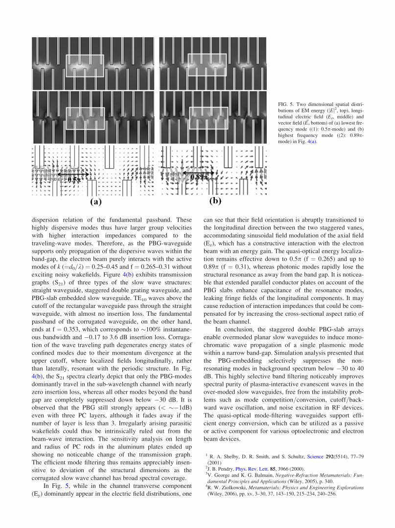
dispersion relation of the fundamental passband. These
highly dispersive modes thus have larger group velocities
with higher interaction impedances compared to the
traveling-wave modes. Therefore, as the PBG-waveguide
supports only propagation of the dispersive waves within the
band-gap, the electron beam purely interacts with the active
modes of k (¼d0=k) ¼ 0.25–0.45 and f ¼ 0.265–0.31 without
exciting noisy wakefields. Figure 4(b) exhibits transmission
graphs (S21) of three types of the slow wave structures:
straight waveguide, staggered double grating waveguide, and
PBG-slab embedded slow waveguide. TE10 waves above the
cutoff of the rectangular waveguide pass through the straight
waveguide, with almost no insertion loss. The fundamental
passband of the corrugated waveguide, on the other hand,
ends at f ¼ 0.353, which corresponds to �100% instantane-
ous bandwidth and �0.17 to 3.6 dB insertion loss. Corruga-
tion of the wave traveling path degenerates energy states of
confined modes due to their momentum divergence at the
upper cutoff, where localized fields longitudinally, rather
than laterally, resonant with the periodic structure. In Fig.
4(b), the S21 spectra clearly depict that only the PBG-modes
dominantly travel in the sub-wavelength channel with nearly
zero insertion loss, whereas all other modes beyond the band
gap are completely suppressed down below �30 dB. It is
observed that the PBG still strongly appears (< ��1dB)
even with three PC layers, although it fades away if the
number of layer is less than 3. Irregularly arising parasitic
wakefields could thus be intrinsically ruled out from the
beam-wave interaction. The sensitivity analysis on length
and radius of PC rods in the aluminum plates ended up
showing no noticeable change of the transmission graph.
The efficient mode filtering thus remains appreciably insen-
sitive to deviation of the structural dimensions as the
corrugated slow wave channel has broad spectral coverage.
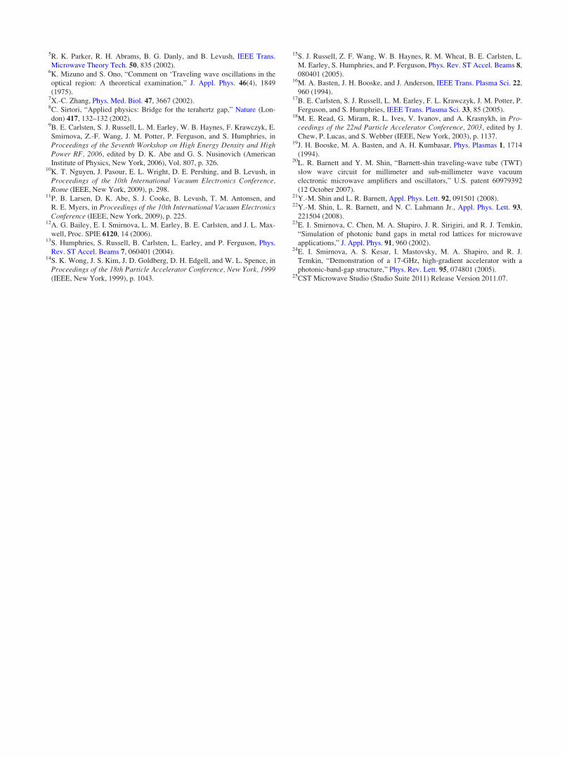
In Fig. 5, while in the channel transverse component
(Ey) dominantly appear in the electric field distributions, one
can see that their field orientation is abruptly transitioned to
the longitudinal direction between the two staggered vanes,
accommodating sinusoidal field modulation of the axial field
(Ez), which has a constructive interaction with the electron
beam with an energy gain. The quasi-optical energy localiza-
tion remains effective down to 0.5p (f ¼ 0.265) and up to
0.89p (f ¼ 0.31), whereas photonic modes rapidly lose the
structural resonance as away from the band gap. It is noticea-
ble that extended parallel conductor plates on account of the
PBG slabs enhance capacitance of the resonance modes,
leaking fringe fields of the longitudinal components. It may
cause reduction of interaction impedances that could be com-
pensated for by increasing the cross-sectional aspect ratio of
the beam channel.
In conclusion, the staggered double PBG-slab arrays
enable overmoded planar slow waveguides to induce mono-
chromatic wave propagation of a single plasmonic mode
within a narrow band-gap. Simulation analysis presented that
the PBG-embedding selectively suppresses the non-
resonating modes in background spectrum below �30 to 40
dB. This highly selective band filtering noticeably improves
spectral purity of plasma-interactive evanescent waves in the
over-moded slow waveguides, free from the instability prob-
lems such as mode competition=conversion, cutoff=back-
ward wave oscillation, and noise excitation in RF devices.
The quasi-optical mode-filtering waveguides support effi-
cient energy conversion, which can be utilized as a passive
or active component for various optoelectronic and electron
beam devices.
1 R. A. Shelby, D. R. Smith, and S. Schultz, Science 292(5514), 77–79
(2001)2J. B. Pendry, Phys. Rev. Lett. 85, 3966 (2000).3V. George and K. G. Balmain, Negative-Refraction Metamaterials: Fun-damental Principles and Applications (Wiley, 2005), p. 340.
4R. W. Ziolkowski, Metamaterials: Physics and Engineering Explorations(Wiley, 2006), pp. xv, 3–30, 37, 143–150, 215–234, 240–256.
FIG. 5. Two dimensional spatial distri-
butions of EM energy (jEj2, top), longi-
tudinal electric field (Ez, middle) and
vector field (~E, bottom) of (a) lowest fre-
quency mode ((1): 0.5p-mode) and (b)
highest frequency mode ((2): 0.89p-
mode) in Fig. 4(a).
5R. K. Parker, R. H. Abrams, B. G. Danly, and B. Levush, IEEE Trans.
Microwave Theory Tech. 50, 835 (2002).6K. Mizuno and S. Ono, “Comment on ‘Traveling wave oscillations in the
optical region: A theoretical examination,” J. Appl. Phys. 46(4), 1849
(1975).7X.-C. Zhang, Phys. Med. Biol. 47, 3667 (2002).8C. Sirtori, “Applied physics: Bridge for the terahertz gap,” Nature (Lon-
don) 417, 132–132 (2002).9B. E. Carlsten, S. J. Russell, L. M. Earley, W. B. Haynes, F. Krawczyk, E.
Smirnova, Z.-F. Wang, J. M. Potter, P. Ferguson, and S. Humphries, in
Proceedings of the Seventh Workshop on High Energy Density and HighPower RF, 2006, edited by D. K. Abe and G. S. Nusinovich (American
Institute of Physics, New York, 2006), Vol. 807, p. 326.10K. T. Nguyen, J. Pasour, E. L. Wright, D. E. Pershing, and B. Levush, in
Proceedings of the 10th International Vacuum Electronics Conference,Rome (IEEE, New York, 2009), p. 298.
11P. B. Larsen, D. K. Abe, S. J. Cooke, B. Levush, T. M. Antonsen, and
R. E. Myers, in Proceedings of the 10th International Vacuum ElectronicsConference (IEEE, New York, 2009), p. 225.
12A. G. Bailey, E. I. Smirnova, L. M. Earley, B. E. Carlsten, and J. L. Max-
well, Proc. SPIE 6120, 14 (2006).13S. Humphries, S. Russell, B. Carlsten, L. Earley, and P. Ferguson, Phys.
Rev. ST Accel. Beams 7, 060401 (2004).14S. K. Wong, J. S. Kim, J. D. Goldberg, D. H. Edgell, and W. L. Spence, in
Proceedings of the 18th Particle Accelerator Conference, New York, 1999(IEEE, New York, 1999), p. 1043.
15S. J. Russell, Z. F. Wang, W. B. Haynes, R. M. Wheat, B. E. Carlsten, L.
M. Earley, S. Humphries, and P. Ferguson, Phys. Rev. ST Accel. Beams 8,
080401 (2005).16M. A. Basten, J. H. Booske, and J. Anderson, IEEE Trans. Plasma Sci. 22,
960 (1994).17B. E. Carlsten, S. J. Russell, L. M. Earley, F. L. Krawczyk, J. M. Potter, P.
Ferguson, and S. Humphries, IEEE Trans. Plasma Sci. 33, 85 (2005).18M. E. Read, G. Miram, R. L. Ives, V. Ivanov, and A. Krasnykh, in Pro-
ceedings of the 22nd Particle Accelerator Conference, 2003, edited by J.
Chew, P. Lucas, and S. Webber (IEEE, New York, 2003), p. 1137.19J. H. Booske, M. A. Basten, and A. H. Kumbasar, Phys. Plasmas 1, 1714
(1994).20L. R. Barnett and Y. M. Shin, “Barnett-shin traveling-wave tube (TWT)
slow wave circuit for millimeter and sub-millimeter wave vacuum
electronic microwave amplifiers and oscillators,” U.S. patent 60979392
(12 October 2007).21Y.-M. Shin and L. R. Barnett, Appl. Phys. Lett. 92, 091501 (2008).22Y.-M. Shin, L. R. Barnett, and N. C. Luhmann Jr., Appl. Phys. Lett. 93,
221504 (2008).23E. I. Smirnova, C. Chen, M. A. Shapiro, J. R. Sirigiri, and R. J. Temkin,
“Simulation of photonic band gaps in metal rod lattices for microwave
applications,” J. Appl. Phys. 91, 960 (2002).24E. I. Smirnova, A. S. Kesar, I. Mastovsky, M. A. Shapiro, and R. J.
Temkin, “Demonstration of a 17-GHz, high-gradient accelerator with a
photonic-band-gap structure,” Phys. Rev. Lett. 95, 074801 (2005).25CST Microwave Studio (Studio Suite 2011) Release Version 2011.07.


![Enhancing the Angular Sensitivity of Plasmonic Sensors ...biotheory.phys.cwru.edu/PDF/AOM.pdf · ultrasensitive plasmonic biosensors.[29,30] A plasmonic nanorod metamaterial (Type](https://img.pdfslide.net/doc/110x75/5fcdd2c6db367d06a677e7be/enhancing-the-angular-sensitivity-of-plasmonic-sensors-ultrasensitive-plasmonic.jpg)