Embed Size (px)
Citation preview
Frequency Table Computation on Dataflow Architecture
P. Škoda*, V. Sruk**, and B. Medved Rogina* * Ruđer Bošković Institute, Zagreb, Croatia
** Faculty of Electrical Engineering and Computing, University of Zagreb, Zagreb, Croatia [email protected]
Abstract – Frequency table computation is a key step in
decision tree learning algorithms. In this paper we present a
novel implementation targeted for dataflow architecture
implemented on field programmable gate array (FPGA).
Consistent with dataflow model of computation, the kernel
views input dataset as synchronous streams of attributes
and class values. The kernel was benchmarked using key
functions from C4.5 program for decision tree learning. For
large datasets with many attributes – over 100,000 items,
and over 60 attributes – the realized kernel, clocked at
333 MHz, outperforms the software implementation
running on CPU clocked at 3.2 GHz.
Keywords – frequency table, dataflow, field programmable
gate arrays, decision tree learning
I. INTRODUCTION
Histogram computation is one of the fundamental procedures used in many data mining algorithms. Its two-dimensional extension – frequency table computation – is a key part of the attribute selection step in decision tree learning algorithms [1]. Decision tree learning algorithms, as well as all other tools used in data mining, are faced with ever-growing size of analyzed datasets. This drives efforts to parallelize existing algorithms, develop new algorithms targeted for parallel and distributed computer systems, and develop new hardware platforms that provide high computational power [2].
One platform that is now gaining more ground in computing applications is field programmable gate array (FPGA). FPGAs are digital integrated circuits designed to be user-configured after manufacturing [3], [4]. An FPGA comprises an array of configurable logic blocks, memory blocks, configurable interconnect, input/output (I/O) blocks, and various specialized arithmetic and communication blocks. These elements together allow implementation of custom computational architectures that can be reconfigured on demand. The computational model that FPGA is most suitable for is the dataflow model.
Majority of computer systems implement a control-flow model of computation. In control-flow, the computation is defined by a sequence of operations that are executed in specified order. In dataflow model, computation is defined by a chain of transformations applied to a stream of data [5]. The dataflow is described spatially in form of dataflow graph. Each operation is
represented by a node, and data flow between nodes is represented by edges. Dataflow graph naturally maps to hardware implementation. Operations are translated into hardware blocks that work concurrently, and edges are translated into data links. By dividing the graph into stages separated by registers, it is transformed into a pipelined structure suitable for implementing on FPGAs.
In this paper we present a novel implementation of frequency table computation targeted for dataflow architecture realized on FPGA. The kernel is developed for integration in C4.5 decision tree learning program [6], [7]. Frequency table computation is a key step in decision tree learning algorithms. Its result is used to calculate dataset split quality, usually Gini impurity or an entropy based measure such as information gain, which is then used for attribute test selection [1].
II. RELATED WORK
Frequency table computation on FPGA has been previously published as a part of efforts in implementing decision tree learning algorithms. FPGAs have been proven to be suitable of implementing data mining algorithms, though so far little attention has been directed to decision tree learning algorithms. Only a few attempts of using FPGAs to accelerate execution of decision tree learning have been reported [8], [9].
Chrysos et al. [9] implement frequency table computation on FPGA as part of HC-CART system for learning decision trees. Frequency table computation is implemented in Frequency Counting module. The module receives attribute-class label pairs. The pairs are used to generate addresses for frequency table locations which contents are then incremented by one. The contents of the frequency table are then copied over to other two auxiliary memories, and used to generate item frequencies for computing Gini impurity. In their implementation, all attribute-class labels received by the kernel have to be prepared by program running on CPU, and then preloaded to memory attached to FPGA. Input data is transferred from CPU to FPGA memory many times in the course of program execution. In our work, the data is transferred to FPGA memory (LMem) only once, at the beginning of the program. The kernel reads the data only from FPGA memory, and the only data transfer between kernel and CPU is sending the computed frequency tables to the CPU.
MIPRO 2014/DC-VIS 357

III. DATAFLOW ENGINE ARCHITECTURE
The Data Flow Engine (DFE) is programmed with one or more kernels and a manager. Kernel implements computation. It defines the computational architecture with scalar and stream inputs and outputs. Manager organizes data movement within the DFE. In managers, the kernels are instantiated and links to off-chip RAM (LMem), CPU or other DFEs are defined.
A. Maxeler Vectis-Lite FPGA platform
Maxeler platform is designed for implementing compute engines using the dataflow model of computation. The platform comprises an FPGA board, drivers, development tools, and API. Dataflow engine is described in Java, using API which provides objects and methods that can be compiled into hardware structures. The compilers translate the input Java code into VHDL code and create functions that implement interface for CPU code [10].
Maxeler Vectis-Lite board was used for realization of the DFE on FPGA. The board is a PCIe expansion board which houses an FPGA, and SDRAM. Basic information on the board is shown in Table I.
B. Kernel architecture
Architecture of the ComputeFreq kernel is shown in
Fig. 1. The kernel has two scalar inputs for parameters: stream length (strmLen), and number of items (items). Stream length is the number of elements read from LMem, which requires all memory accesses to be made in 96 byte blocks. Number of items is the actual number of items of interest in the stream.
The kernel receives two 32 bit unsigned integer streams as input – one for attribute values (att) and the other for class values (attClass) of the items. The inputs are sliced so that the low NA bits are taken from attribute and NC bits from class value. The sliced inputs are concatenated to form the frequency table index, with.
Frequency table is stored in block RAM (BRAM). The BRAM is addressed by the frequency table index formed from attribute and class values. The value output from the BRAM is incremented by one and written back to the same location. The BRAM is configured as a single port RAM with read-first synchronization. The compiler tool automatically inserts registers in appropriate locations, which leads to latency inside the loop. To accommodate this latency, kernel’s input streams are throttled to allow input of one element every m clocks, where m is the length of loop latency.
After all elements of interest are streamed in, contents of the BRAM are streamed out to the CPU through stream output s and at the same time reset to zero. This is achieved by using multiplexers to switch BRAM address port from table index to values generated by a counter. In the same manner the BRAM write data port is switched from incremented-by-one value to constant zero. Since there are no loop dependencies in this instance, the output stream is not throttled. One element is output every single clock. At the same time, any remaining elements in the input streams are read un-throttled (one per clock) and ignored. They are all read to ensure proper functioning of the DFE.
C. Manager
A single ComputeFreq kernel is instantiated in manager. Stream inputs att and attClass are linked to LMem, and use linear memory access pattern. Stream output s is linked to CPU. Scalar inputs items and srtmLen are also linked to CPU. The kernel parameters were set for up to 64 unique attribute and class values (NA = 6, NC = 6). The manager clock frequency was set at 100 MHz, while kernel clock frequency was set at 333 MHz.
DFE interface defines inputs for source addresses of data for input streams att and attClass, values for scalar inputs items and srtmLen, and destination address for output stream s.
With given parameters, frequency table stores 4096 32-bit words. Loop latency of the synthesized design is 5
TABLE I. BASIC INFORMATION ON MAXELER VECTIS-LITE FPGA BOARD
FPGA Xilinx Virtex-6 XCVSX475T
Off-chip RAM (LMem) 6 GiB (6×1 GiB) DDR2-800 SDRAM
On-chip RAM (FMem) ~ 4 MiB Block RAM
CPU ↔ FPGA bandwidth 2 GB/s
LMem ↔ FPGA bandwidth 38.4 GB/s max.
Figure 1. ComputeFreq kernel architecture for up to 64 unique
attribute and class values (NA = 6, NC = 6).
TABLE II. FPGA RESOURCE USAGE BY THE DFE
Resource Used Total available Utilization
LUTs 30053 297600 10.10 %
Flip-flops 43416 297600 14.59 %
DSP blocks 0 2016 0.00 %
Block RAM 105 2128 4.93 %
358 MIPRO 2014/DC-VIS
clocks, which means that the DFE can process up to 66.6×10⁶ items per second. FPGA resource usage by the DFE is given in Table II.
IV. EXPERIMENTAL RESULTS
A. Benchmarks and test environment
Kernel was benchmarked by using code from C4.5 Release 8 decision tree learning program [11]. The normal tree building features from the original program were disabled. Only parts required for loading datasets and computing the frequency table were left operational. A function was added for transforming dataset into format appropriate for DFE and writing it to LMem. Time measurement was added to ComputeFrequencies function. For execution on DFE, the ComputeFrequencies function was modified to use function calls to the DFE, and copy the received result into the original frequency table data structure. From measured execution time, the function’s throughput was computed by:
ia
iat
iaT
,, = (1)
where a is number of attributes, i is number of items, ta,i is measured execution time, and Ta,i is throughput for dataset with a attributes and i items.
A set of 84 datasets was generated for the benchmark. All datasets have only nominal attributes with 63 unique attribute values (values from 1 to 63), and 64 unique class values (from 0 to 63). Number of items vary exponentially from 2×210 to 4×220 (211 – 222) items, while number of attributes varies exponentially from 1 to 64 (20 – 26). Attribute and class values are generated randomly using uniform distribution.
Benchmark program was compiled using gcc compiler version 4.4.7. Benchmarks were run on workstation with Intel Xeon E5-1650 CPU running at 3.2 GHz, 16 GiB DDR3-1600 RAM, under Centos 6.5 Linux OS. The workstation is equipped with Maxeler Vectis-Lite FPGA acceleration board.
B. ComputeFrequencies CPU benchmark results
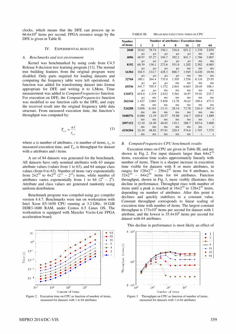
Execution times on CPU are given in Table III, and are shown in Fig. 2. For input datasets larger than 64×210 items, execution time scales approximately linearly with number of items. There is a sharper increase in execution time visible for datasets with 8 or more attributes, in ranges for 128×210 – 256×210 items for 8 attributes, to 32×210 – 64×210 items for 64 attributes. Function throughput, shown in Fig. 3, more visibly illustrates this decline in performance. Throughput rises with number of items until a peak is reached at 16×210 to 128×210 items, depending on number of attributes. After this point it declines and quickly stabilizes to a constant value. Constant throughput corresponds to linear scaling of execution time with number of items. The largest constant throughput is 173×106 items per second for dataset with 1 attribute, and the lowest is 35.4×10⁶ items per second for dataset with 64 attributes.
This decline in performance is most likely an effect of
Figure 2. Execution time on CPU as function of number of items,
measured for datasets with 1 to 64 attributes
TABLE III. MEASURED EXECUTION TIMES ON CPU
Number
of items
Number of attributes / Execution time
1 2 4 8 16 32 64
2048 39.62 µs
78.74 µs
156.1 µs
316.6 µs
651.2 µs
1.339 ms
2.859 ms
4096 48.97 µs
97.27 µs
194.7 µs
392.2 µs
841.7 µs
1.766 ms
3.807 ms
8192 68.39 µs
136.1 µs
273.6 µs
551.0 µs
1.202 ms
2.582 ms
6.065 ms
16384 104.5 µs
214.7 µs
428.3 µs
866.7 µs
1.945 ms
4.420 ms
10.94 ms
32768 180.1 µs
364.4 µs
735.0 µs
1.505 ms
3.556 ms
8.116 ms
25.95 ms
65536 341.7 µs
705.5 µs
1.372 ms
2.841 ms
6.663 ms
20.45 ms
108.1 ms
131072 654.0 µs
1.319 ms
2.632 ms
5.561 ms
16.97 ms
55.01 ms
235.7 ms
262144 1.427 ms
2.885 ms
5.858 ms
13.78 ms
36.63 ms
109.4 ms
473.5 ms
524288 3.056 ms
6.161 ms
13.11 ms
28.14 ms
72.70 ms
216.4 ms
947.4 ms
1048576 6.080 ms
12.19 ms
24.57 ms
55.80 ms
144.7 ms
428.8 ms
1.889 s
2097152 12.10 ms
24.49 ms
48.83 ms
110.1 ms
288.7 ms
855.6 ms
3.800 s
4194304 24.30 ms
48.82 ms
97.81 ms
220.5 ms
574.6 ms
1.707 s
7.575 s
Figure 3. Throughput on CPU as function of number of items,
measured for datasets with 1 to 64 attributes
MIPRO 2014/DC-VIS 359
CPU’s cache system. Smaller sets are less affected by cache misses than larger sets. In addition, the dataset is stored in attribute major order. Since ComputeFrequencies function works by accessing the same attribute over different items, this leads to consecutive accesses to non-consecutive memory locations, which are more likely to result in cache misses.
C. ComputeFrequencies DFE benchmark results
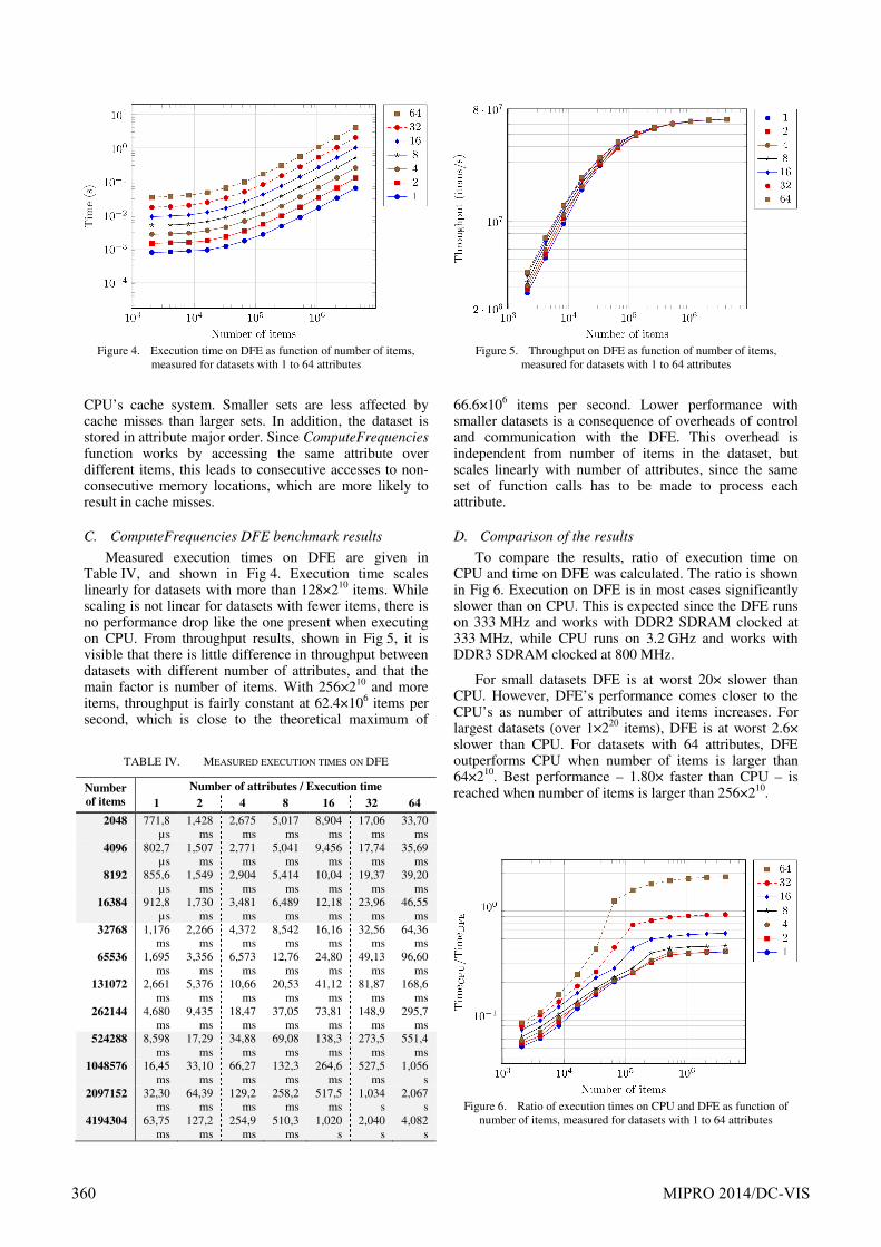
Measured execution times on DFE are given in Table IV, and shown in Fig 4. Execution time scales linearly for datasets with more than 128×210 items. While scaling is not linear for datasets with fewer items, there is no performance drop like the one present when executing on CPU. From throughput results, shown in Fig 5, it is visible that there is little difference in throughput between datasets with different number of attributes, and that the main factor is number of items. With 256×210 and more items, throughput is fairly constant at 62.4×10⁶ items per second, which is close to the theoretical maximum of
66.6×10⁶ items per second. Lower performance with smaller datasets is a consequence of overheads of control and communication with the DFE. This overhead is independent from number of items in the dataset, but scales linearly with number of attributes, since the same set of function calls has to be made to process each attribute.
D. Comparison of the results
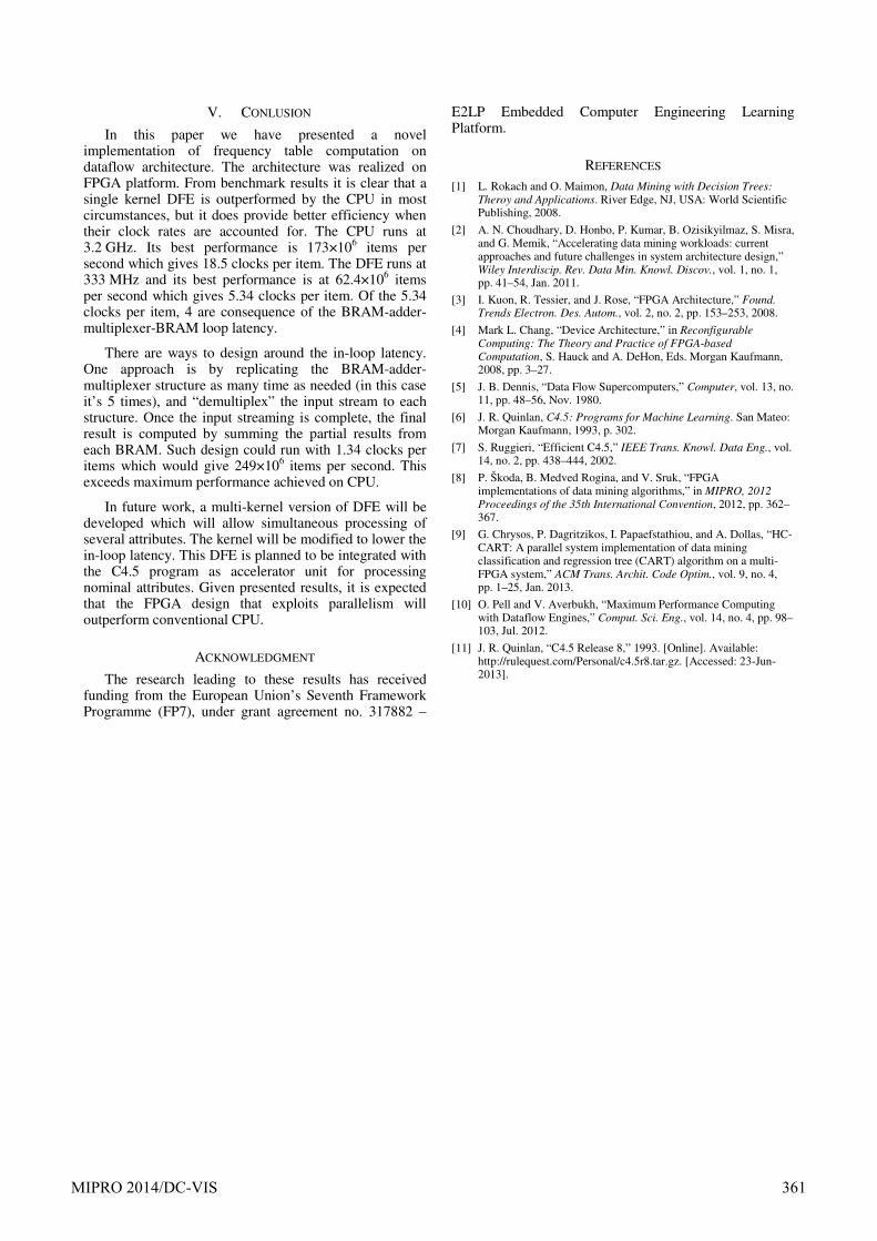
To compare the results, ratio of execution time on CPU and time on DFE was calculated. The ratio is shown in Fig 6. Execution on DFE is in most cases significantly slower than on CPU. This is expected since the DFE runs on 333 MHz and works with DDR2 SDRAM clocked at 333 MHz, while CPU runs on 3.2 GHz and works with DDR3 SDRAM clocked at 800 MHz.
For small datasets DFE is at worst 20× slower than CPU. However, DFE’s performance comes closer to the CPU’s as number of attributes and items increases. For largest datasets (over 1×220 items), DFE is at worst 2.6× slower than CPU. For datasets with 64 attributes, DFE outperforms CPU when number of items is larger than 64×210. Best performance – 1.80× faster than CPU – is reached when number of items is larger than 256×210.
Figure 4. Execution time on DFE as function of number of items,
measured for datasets with 1 to 64 attributes
Figure 5. Throughput on DFE as function of number of items,
measured for datasets with 1 to 64 attributes
TABLE IV. MEASURED EXECUTION TIMES ON DFE
Number
of items
Number of attributes / Execution time
1 2 4 8 16 32 64
2048 771,8 µs
1,428 ms
2,675 ms
5,017 ms
8,904 ms
17,06 ms
33,70 ms
4096 802,7 µs
1,507 ms
2,771 ms
5,041 ms
9,456 ms
17,74 ms
35,69 ms
8192 855,6 µs
1,549 ms
2,904 ms
5,414 ms
10,04 ms
19,37 ms
39,20 ms
16384 912,8 µs
1,730 ms
3,481 ms
6,489 ms
12,18 ms
23,96 ms
46,55 ms
32768 1,176 ms
2,266 ms
4,372 ms
8,542 ms
16,16 ms
32,56 ms
64,36 ms
65536 1,695 ms
3,356 ms
6,573 ms
12,76 ms
24,80 ms
49,13 ms
96,60 ms
131072 2,661 ms
5,376 ms
10,66 ms
20,53 ms
41,12 ms
81,87 ms
168,6 ms
262144 4,680 ms
9,435 ms
18,47 ms
37,05 ms
73,81 ms
148,9 ms
295,7 ms
524288 8,598 ms
17,29 ms
34,88 ms
69,08 ms
138,3 ms
273,5 ms
551,4 ms
1048576 16,45 ms
33,10 ms
66,27 ms
132,3 ms
264,6 ms
527,5 ms
1,056 s
2097152 32,30 ms
64,39 ms
129,2 ms
258,2 ms
517,5 ms
1,034 s
2,067 s
4194304 63,75 ms
127,2 ms
254,9 ms
510,3 ms
1,020 s
2,040 s
4,082 s
Figure 6. Ratio of execution times on CPU and DFE as function of
number of items, measured for datasets with 1 to 64 attributes
360 MIPRO 2014/DC-VIS
V. CONLUSION
In this paper we have presented a novel implementation of frequency table computation on dataflow architecture. The architecture was realized on FPGA platform. From benchmark results it is clear that a single kernel DFE is outperformed by the CPU in most circumstances, but it does provide better efficiency when their clock rates are accounted for. The CPU runs at 3.2 GHz. Its best performance is 173×106 items per second which gives 18.5 clocks per item. The DFE runs at 333 MHz and its best performance is at 62.4×10⁶ items per second which gives 5.34 clocks per item. Of the 5.34 clocks per item, 4 are consequence of the BRAM-adder-multiplexer-BRAM loop latency.
There are ways to design around the in-loop latency. One approach is by replicating the BRAM-adder-multiplexer structure as many time as needed (in this case it’s 5 times), and “demultiplex” the input stream to each structure. Once the input streaming is complete, the final result is computed by summing the partial results from each BRAM. Such design could run with 1.34 clocks per items which would give 249×106 items per second. This exceeds maximum performance achieved on CPU.
In future work, a multi-kernel version of DFE will be developed which will allow simultaneous processing of several attributes. The kernel will be modified to lower the in-loop latency. This DFE is planned to be integrated with the C4.5 program as accelerator unit for processing nominal attributes. Given presented results, it is expected that the FPGA design that exploits parallelism will outperform conventional CPU.
ACKNOWLEDGMENT
The research leading to these results has received funding from the European Union’s Seventh Framework Programme (FP7), under grant agreement no. 317882 –
E2LP Embedded Computer Engineering Learning Platform.
REFERENCES [1] L. Rokach and O. Maimon, Data Mining with Decision Trees:
Theroy and Applications. River Edge, NJ, USA: World Scientific Publishing, 2008.
[2] A. N. Choudhary, D. Honbo, P. Kumar, B. Ozisikyilmaz, S. Misra, and G. Memik, “Accelerating data mining workloads: current approaches and future challenges in system architecture design,” Wiley Interdiscip. Rev. Data Min. Knowl. Discov., vol. 1, no. 1, pp. 41–54, Jan. 2011.
[3] I. Kuon, R. Tessier, and J. Rose, “FPGA Architecture,” Found. Trends Electron. Des. Autom., vol. 2, no. 2, pp. 153–253, 2008.
[4] Mark L. Chang, “Device Architecture,” in Reconfigurable
Computing: The Theory and Practice of FPGA-based
Computation, S. Hauck and A. DeHon, Eds. Morgan Kaufmann, 2008, pp. 3–27.
[5] J. B. Dennis, “Data Flow Supercomputers,” Computer, vol. 13, no. 11, pp. 48–56, Nov. 1980.
[6] J. R. Quinlan, C4.5: Programs for Machine Learning. San Mateo: Morgan Kaufmann, 1993, p. 302.
[7] S. Ruggieri, “Efficient C4.5,” IEEE Trans. Knowl. Data Eng., vol. 14, no. 2, pp. 438–444, 2002.
[8] P. Škoda, B. Medved Rogina, and V. Sruk, “FPGA implementations of data mining algorithms,” in MIPRO, 2012
Proceedings of the 35th International Convention, 2012, pp. 362–367.
[9] G. Chrysos, P. Dagritzikos, I. Papaefstathiou, and A. Dollas, “HC-CART: A parallel system implementation of data mining classification and regression tree (CART) algorithm on a multi-FPGA system,” ACM Trans. Archit. Code Optim., vol. 9, no. 4, pp. 1–25, Jan. 2013.
[10] O. Pell and V. Averbukh, “Maximum Performance Computing with Dataflow Engines,” Comput. Sci. Eng., vol. 14, no. 4, pp. 98–103, Jul. 2012.
[11] J. R. Quinlan, “C4.5 Release 8,” 1993. [Online]. Available: http://rulequest.com/Personal/c4.5r8.tar.gz. [Accessed: 23-Jun-2013].
MIPRO 2014/DC-VIS 361