Embed Size (px)
Citation preview


What are dummy components?*Dummy components are the exact mechanical equivalent of functional electronic components.
Why use dummy components?Dummies save money. In cases where only mechanical characteristics are required, dummy components can be used instead of live functioning components. Since there is no expensive die inside the package, the cost for performing mechanical testing is significantly lower.
Who is Practical Components?Practical Components is a team of dedicated electronic industry professionals offering value pricing, on-time delivery, and superior service to our customers. The Practical Components team is ready to provide project assistance in the areas of technical component knowledge, drawings, component land patterns, and PCB practice kits.
What is a PCB Practice Kit?A PCB Practice Kit contains both the PC practice board and the necessary dummy components so customers can conduct assembly process evaluation without using high-cost, live components and functional PC boards. Kits are available in a single pack for employee hand soldering training or packaged for production equipment evaluation. Both X, Y Theta data and Gerber data are available without charge.
What other products are offered by Practical Components?In addition to dummy components, Practical carries solder training aids, tools and related equipment, IPC products and designs custom printed circuit boards. Your sales representative can supply technical information and pricing on all our products.
Who uses dummy components?Companies that are involved with electronic component assembly, testing, evaluation and employee training.
Frequently Asked Questions
Contact Practical Components
* Disclaimer: Dummy components are only to be used for evaluation and testing purposes. Practical Components is not responsible for product that is used as a “live” package using live die assembly. Dummy samples are not to be used for 1st reliability testing.
Distributor of mechanical IC samples (dummy components), test boards, kits and SMD production tools and equipment.
If you have any additional questions concerning Practical Components, our products or policies, please contact us.
Practical Components, Inc. 10762 Noel Street Los Alamitos, CA 90720 USA Tel: 1-714-252-0010 Fax: 1-714-252-0026 E-mail: [email protected] Web Site: www.PracticalComponents.com www.TrustPCI.com
Main E-mail................................................................................ [email protected] ............................................................. Russell Kido / [email protected] .................................................................... Kym Bell / [email protected] ......................................................... Lisa Laphen / [email protected] Support .................................................. [email protected]/Distributors .....Deanne Guzman / [email protected] ............................................Kevin Laphen / [email protected]
Practical Components is the exclusive distributor of Amkor Technology Mechanical Components.

Bill / Remit to: Practical Components, Inc. PO Box 1037 Los Alamitos, CA 90720-1037 USA
Ship to: Practical Components, Inc. 10762 Noel Street Los Alamitos, CA 90720 USA
Tel: 1-714-252-0010 Fax: 1-714-252-0026 E-mail: [email protected] Web Site: www.TrustPCI.com
F.O.B. is Los Alamitos, CA USA
Terms and ConditionsOut Of Stock Items: Items not available for immediate shipment will be shipped as they become available. Items not available at the end of 90 days will be cancelled. The number of back-ordered days may be extended beyond 90 days with customer approval.
Return Policy: Returns must be made promptly and accompanied by a return authorization number. Please contact a customer service representative to obtain a return authorization number. All returns must be made within 30 days of date of invoice and accompanied by return authorization number.
� Return freight charges must be prepaid. � C.O.D. returns cannot be accepted. � Return merchandise in original packaging and in
resalable condition. � Please note that items returned due to customer error may be subject
to a restocking charge of 25%. � Non-catalog items are not returnable.
Catalog Listings: Not all products listed in this catalog are maintained in stock, and all product specifications for each product are current as of the date of publication. Product listings, specifications and prices for each product are subject to change without notice.
How To Place Your OrderOur sales staff is ready to serve you from 8:00 A.M. to 5 P. M. Pacific Standard Time, Monday through Friday. Our fax lines are open 24 hours every day.
Fax and E-mail orders received after normal business hours are processed the next business day. Please include your telephone and fax numbers so we can confirm your order.
Our website www.TrustPCI.com is always available and is loaded with valuable information about our products including detailed component drawings, daisy-chain patterns, white papers, photos and data sheets. The site has many products such as hand solder training kits available for purchase online.
Product Liability: Practical Components’ sole obligation for products that prove to be defective within 10 days of purchase will be replaced or refunded. Practical Components gives no warranty either expressed or implied and specifically disclaims all other warranties, including warranties for merchantability and fitness.
In no event shall Practical Components’ liability exceed the buyer’s purchase price nor shall Practical Components be liable for any indirect or consequential damages.
Shipment Damage: Merchandise is carefully packaged in compliance with carrier requirements. Claims for loss or damage in transit must be made with the carrier by the customer. All shipments should be unpacked and inspected immediately upon receipt. If damage does not become apparent until shipment is unpacked, make a request for inspection by the carrier’s agent. Failure to do so will result in the carrier refusing to honor the claim.
Non-Catalog Items: Merchandise not listed in our catalog, if available from our suppliers, may be subject to minimum order quantities and/or special handling charges. Shipment is made as quickly as deliveries are received from our suppliers. Special order products are sold on a non-returnable basis.
Quotations: All items are subject to prior sale. A quote is valid for 30 days.
Dishonored Check Policy: If a check you give us as payment is dishonored for any reason by the bank or any other institution on which it is drawn, you agree to pay us $20.00 as a service charge. In addition, you agree to pay any other reasonable charges imposed by any check verification company or collection agency that we may use for collection.
Prices/Quantities: Prices are subject to change without notice and quantities may be limited.
Handling Charge: A $10.00 handling charge applies to all orders less than $50.00.
Terms: We accept Visa, MasterCard and American Express (minimum order is $50.00).
Open Account: We bill on a net 30–day basis to customers with approved credit.
Large Quantity Quotations: Practical Components will be happy to quote quantities in excess of the amounts shown in the catalog.
Freight Charges: On open accounts, actual freight charges are added to the invoice. A packing and handling fee of $5.00 is added to the order. C.O.D accounts will have the freight charges pre-billed to the C.O.D. total in addition to a $5.00 packing and handling charge.
Tray Charge: A $8.00 tray charge is added if customer orders less than a full tray quantity.
Special Requirements: Please include specific instructions if you require special packing, marking, shipping, routing or insurance.
*All prices are in USD ($).

Table of Contents
Flip ChipsCSPnl (RDL) Wafer ......................................................................................................4eWLP Embeded Wafer Level Package .................................................................5WLP ....................................................................................................................................6WLP ....................................................................................................................................7Flip Chips .........................................................................................................................8Pac Tech Flip Chip .......................................................................................................9
Ball Grid ArrayCVBGA ............................................................................................................................ 10PCB368- .3 mm Pitch CVBGA ............................................................................... 11CTBGA ............................................................................................................................ 12CABGA ............................................................................................................................ 13PBGA ............................................................................................................................... 14SBGA ............................................................................................................................... 15
Land Grid ArrayLGA .................................................................................................................................. 16
Through Mold ViaTMV® PoP .................................................................................................................... 17TMV® 14mm Board & Kit ...................................................................................... 21
Package on Package (PoP)PoP................................................................................................................................... 22Package on Package (PoP) .................................................................................... 23PoP 12mm Board and Kit ...................................................................................... 31Package on Package (PoP) .................................................................................... 32PoP 14mm Board & Kit ........................................................................................... 35
OmQFNOmQFN .......................................................................................................................... 36
MicroLead FrameMLF® MicroLeadFrame® ....................................................................................... 37Dual Row MLF® ......................................................................................................... 38
Quad Flat PacksTQFP ............................................................................................................................... 39LQFP ............................................................................................................................... 40QFP .................................................................................................................................. 41CQFP ............................................................................................................................... 42LCC................................................................................................................................... 42Daisy-Chain Patterns ............................................................................................... 43
Dual PackagesPLCC ................................................................................................................................ 44SOIC ................................................................................................................................. 45TSOP ............................................................................................................................... 46TSSOP ............................................................................................................................. 47SSOP ................................................................................................................................ 48
Advanced Wafer TechnologyAdvanced Wafer Packages ..................................................................................... 50Advanced Wafer Technology Substrates ......................................................... 71
Tape & ReelCTReels .......................................................................................................................... 72Tape and Reel Specifications ................................................................................ 73
Through-HolePDIP ................................................................................................................................ 74Through-Hole Glass Diodes .................................................................................. 74Through-Hole Transistors ..................................................................................... 75Axial Leaded Resistors ............................................................................................ 75
Passives, Resistors, DiscretesSMT ................................................................................................................................. 76SMR ................................................................................................................................. 78SMC ................................................................................................................................. 79Ceramic Chip Pad Components ........................................................................... 80MELF Resistors .......................................................................................................... 80SME ................................................................................................................................. 81MELF Diodes ............................................................................................................... 81SMTA ............................................................................................................................... 82
Practical Production ToolsCircuitMedic ................................................................................................................ 83
Printed Circuit Boards & KitsKit Identifier ................................................................................................................ 84Custom PC Practice Boards and Kits ................................................................ 87Conformal Coating Process Flow Chart ........................................................... 88Test Boards for Cleanliness and Conformal Coating .................................. 89SIR Test Board and Kit ............................................................................................ 92SMTA Saber Evaluation Board and Kit ............................................................. 93B-52 CRET Rev B ....................................................................................................... 94Single Pack Hand Solder Kit ................................................................................. 96Solder Practice Board and Kit .............................................................................. 97Mixed Technology Board and Kit ....................................................................... 98Through-Hole Solder Training Kits ................................................................... 99Rework Kits ...............................................................................................................100IPC Compliant Hand Soldering Kit ..................................................................101Terminal and Wire Kit...........................................................................................102IPC/WHMA-A620 Wire Harness Kit ...............................................................103Solder Practice Board and Kits .........................................................................104Foresite Umpire Test Board ................................................................................106Jabil Solder Paste Evaluation ............................................................................107AIM Print Test Board and Kit .............................................................................108Lead-Free Zero-Ohm SMD Resistor Kit .........................................................109MLF® Test Board and Kits ...................................................................................110BGA Variable Pitch and Array Board ..............................................................112BGA Fine Pitch Board and Kit ............................................................................113BGA Global Daisy-Chain Test Kit ......................................................................114Process Capability Validation Kit .....................................................................116SMT/PTH ....................................................................................................................117IPC 9850 Attribute Defect Rate Kit ..................................................................118CircuitCAM™ Software ..........................................................................................119
Distributor InformationInternational Distributors ...................................................................................120

4 Practical Components, Inc. • www.TrustPCI.com • [email protected]
Practical Components introduces new CSPnl (RDL) dummy wafers from Amkor. The CSPnl Bump on Redistribution (RDL) option adds a plated copper redistribution layer to route I/O pads to JEDEC/EIAJ standard pitches, avoiding the need to redesign legacy parts for CSP applications. Nickel-based or copper UBM is offered, along with polyimide or PBO repassivation. CSPnl with RDL utilizes industry-standard surface mount assembly and reflow techniques, and does not require underfill.
This 8 inch wafer can be provided diced into individual die or as an uncut wafer. The wafer can be provided with SAC405 bumps.
Pad pitch is 400um (0.4mm). Wafer thickness is 725um, with back grinding available to 200um.
Pads on this wafer are daisy chained and can be cut to any sized request. Packaging is tape and reel bumps down for cut die or cut and in the ring. Uncut 8inch wafers are shipped in plastic wafer packs. There is a lot of flexibility with this type of component.
In addition to the wafer Practical Components can also provide a test board (substrate) on request.
Please call our technical representatives at 714-252-0010 for additional information.
CSPnl (RDL) Wafer
Notes � Trace material: Copper � Trace thickness: 3um � Trace width: 100um � Bump pad shape: Circular / Square � Bump pad size: 225/290um � Tape and Reel: Width = 8mm Pitch = 4mm � 0.3mm & 0.5mm Pitch packages are available. Please call for more
information.
NEW!
Practical Components is the exclusive distributor of Amkor Technology Mechanical Components.
Part Description I/O Count
Die Size Pitch Matrix Projected
Die Yield Alloy
A-CSPnl4-0.76mm-.4mm-DC 4 0.76 .4mm 2x2 40,000 SAC405, No Solder BallA-CSPnl16-1.56mm-.4mm-DC 16 1.56 .4mm 4x4 10,000 SAC405, No Solder BallA-CSPnl36-2.36mm-.4mm-DC 36 2.36 .4mm 6x6 4,500 SAC405, No Solder BallA-CSPnl64-3.16mm-.4mm-DC 64 3.16 .4mm 8x8 2,500 SAC405, No Solder BallA-CSPnl100-3.96mm-.4mm-DC 100 3.96 .4mm 10x10 1,500 SAC405, No Solder BallA-CSPnl144-4.76mm-.4mm-DC 144 4.76 .4mm 12x12 1,000 SAC405, No Solder BallA-CSPnl196-5.56mm-.4mm-DC 196 5.56 .4mm 14x14 500 SAC405, No Solder Ball
� Add “WR” to end of part number for Wafer Cut and left in Seal Ring. � Add “TR” to end of part number for die on Tape and Reel. � Add “NB” to end of part number for No Solder Balls. � Add “SAC405” to end of part number for Lead-Free. � Add “W” to end of part number for Uncut Wafer.
Part Description System
Amkor A CSPnl 100 3.96mm .4mm DC Alloy
Wafer (NB, SAC405)I/O Count
Daisy ChainDie Size
Pitch
Flip Chips

5Practical Components, Inc. • Tel: 1-714-252-0010 • Fax: 1-714-252-0026
NEW!
Practical Components is offering Amkor’s embedded copper posts/pad on a eWLP (embedded Wafer Level Package) 8 inch wafer. eWLP wafers have copper posts that are embedded into the die. Size of the posts is 8um to 10um. Pitch between the copper posts is 400um (0.4mm).
Wafer thickness is 725um and can be back grinded to 200um.
These wafers can be supplied by uncut wafer or cut die, packaged on tape and reel with pads down. Copper pillar dummy test wafers provide an excellent opportunity to investigate the effectiveness of the flip chip die attach process.
Practical Components technical staff can provide additional information on the new Amkor eWLP test wafers. In addition to the wafers and die, Practical can supply test vehicles for the eWLP test die.
Each die is daisy chained and customer can have the wafer cut to match a required die size.
Call for more information: (714) 252-0010
Practical Components is the exclusive distributor of Amkor Technology Mechanical Components.
Part Description I/O Count
Die Size Pitch Matrix Projected
Die Yield Alloy
A-eWLP4-0.76mm-.4mm-DC 4 0.76 .4mm 2x2 40,000 No Solder BallA-eWLP16-1.56mm-.4mm-DC 16 1.56 .4mm 4x4 10,000 No Solder BallA-eWLP36-2.36mm-.4mm-DC 36 2.36 .4mm 6x6 4,500 No Solder BallA-eWLP64-3.16mm-.4mm-DC 64 3.16 .4mm 8x8 2,500 No Solder BallA-eWLP100-3.96mm-.4mm-DC 100 3.96 .4mm 10x10 1,500 No Solder BallA-eWLP144-4.76mm-.4mm-DC 144 4.76 .4mm 12x12 1,000 No Solder BallA-eWLP196-5.56mm-.4mm-DC 196 5.56 .4mm 14x14 500 No Solder Ball
Notes � Ball Place or Electroplated: Electroplated � Bump On Pad or redistribution Layer: Redistribution Layer � Bump Material: Cu bump � Bump Height: 10 um � Bump pitch: 400 um � Bump Shear Strength: >2 g/mil2 � Plating Area 30: 5948 mm2
10: 10804 mm2 � Tape and Reel: Width =8mm Pitch = 4mm � 0.3mm & 0.5mm Pitch packages are available. Please call for more
information.
� Add “WR” to end of part number for Wafer Cut and left in Seal Ring. � Add “TR” to end of part number for die on Tape and Reel. � Add “NB” to end of part number for No Solder Balls. � Add “W” to end of part number for Uncut Wafer.
eWLP Embeded Wafer Level Package
Part Description System
Amkor A eWLP 100 3.96mm .4mm DC Alloy
Embedded Wafer Level NB
I/O CountDaisy Chain
Die SizePitch
6 Practical Components, Inc. • www.TrustPCI.com • [email protected]
WLP uses interconnection technology to effectively utilize the chip area by making it possible to form electrodes over the entire chip surface. This eliminates the need for the wire bonding space required by previous wiring methods. Also, electrodes are formed using copper posts for a simple structure.
All of this means that the area of the finished package is exactly the same compact size as the original chip. It also simplifies mounting and contributes to easier high-density mounting. WLP is the perfect choice for packaging chips used in portable telephones, digital cameras, and other applications where mounting space is severely restricted.
WLPWafer Chip Size Package NEW!
Notes � Ultra thin type, Ultra miniature, Lightweight � High current capacity and good heat radiation � Stress buffer structure � High reliability of WLP as semiconductor package makes KGD
issues cleared. � Cu-to-Cu wiring structure � Include inductors of high Q value � Possibility of SMT assembly � Coplanarity (5 to 10 µm) � Available diced and left in ring or in trays.
Part Description I/O Count Pitch Body
Size Matrix Alloy
.3mm PitchWLP100-.3mm-3mm-DC 100 .3mm 3mm 10x10 96.5%Sn/3.0%Ag/0.5%CuWLP144-.3mm-3.6mm-DC 144 .3mm 3.6mm 12x12 96.5%Sn/3.0%Ag/0.5%CuWLP196-.3mm-4.2mm-DC 196 .3mm 4.2mm 14x14 96.5%Sn/3.0%Ag/0.5%CuWLP256-.3mm-4.8mm-DC 256 .3mm 4.8mm 16x16 96.5%Sn/3.0%Ag/0.5%CuWLP264-.3mm-6mm-DC 264 .3mm 6mm 17x17 96.5%Sn/3.0%Ag/0.5%CuWLP400-.3mm-6mm-DC 400 .3mm 6mm 20x20 96.5%Sn/3.0%Ag/0.5%CuWLP676-.3mm-7.8mm-DC 676 .3mm 7.8mm 26x26 96.5%Sn/3.0%Ag/0.5%CuWLP900-.3mm-9mm-DC 900 .3mm 9mm 30x30 96.5%Sn/3.0%Ag/0.5%CuWLP1600-.3mm-12mm-DC 1600 .3mm 12mm 40x40 96.5%Sn/3.0%Ag/0.5%Cu.4mm PitchWLP100-.4mm-4mm-DC 100 .4mm 4mm 10x10 96.5%Sn/3.0%Ag/0.5%CuWLP144-.4mm-4.8mm-DC 144 .4mm 4.8mm 12x12 96.5%Sn/3.0%Ag/0.5%CuWLP144-.4mm-6mm-DC 144 .4mm 6mm 13x13/4-Row 96.5%Sn/3.0%Ag/0.5%CuWLP196-.4mm-5.6mm-DC 196 .4mm 5.6mm 14x14 96.5%Sn/3.0%Ag/0.5%CuWLP256-.4mm-6.4mm-DC 256 .4mm 6.4mm 16x16 96.5%Sn/3.0%Ag/0.5%CuWLP400-.4mm-8mm-DC 400 .4mm 8mm 20x20 96.5%Sn/3.0%Ag/0.5%CuWLP676-.4mm-10.4mm-DC 676 .4mm 10.4mm 26x26 96.5%Sn/3.0%Ag/0.5%CuWLP900-.4mm-12mm-DC 900 .4mm 12mm 30x30 96.5%Sn/3.0%Ag/0.5%Cu.5mm PitchWLP100-.5mm-5mm-DC 100 .5mm 5mm 10x10 96.5%Sn/3.0%Ag/0.5%CuWLP144-.5mm-6mm-DC 144 .5mm 6mm 12x12 96.5%Sn/3.0%Ag/0.5%CuWLP196-.5mm-7mm-DC 196 .5mm 7mm 14x14 96.5%Sn/3.0%Ag/0.5%CuWLP256-.5mm-8mm-DC 256 .5mm 8mm 16x16 96.5%Sn/3.0%Ag/0.5%CuWLP400-.5mm-10mm-DC 400 .5mm 10mm 20x20 96.5%Sn/3.0%Ag/0.5%CuWLP676-.5mm-13mm-DC 676 .5mm 13mm 26x26 96.5%Sn/3.0%Ag/0.5%CuWLP900-.5mm-15mm-DC 900 .5mm 15mm 30x30 96.5%Sn/3.0%Ag/0.5%Cu
� Add “TR” to end of part number for die on Tape and Reel. � Add “SAC305” to end of part number for Lead-Free.
Part Description System
WLP 196 .3mm 4.2mm DC Alloy
Wafer Chip Size Package (SAC305)
I/O Count Daisy Chain
Pitch Die Size

7Practical Components, Inc. • Tel: 1-714-252-0010 • Fax: 1-714-252-0026
Solder Ball
Cu Bump (Post)
Cu Re-distribution Silicon Substrate
Dicing Surface
Re-passivation
Encapsulation
Protect here byencapsulation
Encapsulation
Cu redistribution +Low-k layer
WLPWafer Chip Size Package
WLP196-.3mm-4.2mm (14x14 Matrix) WLP256-.3mm-4.8mm (16x16 Matrix)
WLP264-.3mm-6mm (17x17 Matrix) WLP400-.3mm-6mm (20x20 Matrix)
Solder Ball
Cu Bump (Post)
Cu Re-distribution Silicon Substrate
Dicing Surface
Re-passivation
Encapsulation
Protect here byencapsulation
Encapsulation
Cu redistribution +Low-k layer
8 Practical Components, Inc. • www.TrustPCI.com • [email protected]
Pac Tech offers a complete set of additional wafer level and backend services including: saw, dice, redistribution, repassivation, backside laser mark, backside coating, test die, and assembly. In addition, Pac Tech has the latest in metrology and analytical equipment to help in the development and production proceses, including: x-ray, shear, AOI, ICP, AA, probing, high speed ball pull, chemical analysis, etc…
Flip Chip describes the method of electrically connecting the die to the package carrier. The package carrier, either substrates or leadframe, then provides the connection from the die to the exterior of the package. The interconnection between die and carrier in flip chip packaging is made through a conductive bump that is placed directly on the die surface. The bumped die is then flipped over and placed face down, with the bumps connecting to the carrier. After the die is solderable, underfill is applied between the die and the substrates, around the solder bumps. The underfill is designed to contract the stress in the solder joints caused by the difference in thermal expansion between the silicon die and carrier.
Notes � Die count represents expected yield per wafer. � All die is packaged in waffle pack trays unless otherwise specified. � The potential multiple is the number of die repears on the wafer. With
the wafer orientated flat down, a right hand coordinate system applies. � Die Size is from scribe line to center-to-center. Scribe width is 0.05mm
Passicated. Each bump is electrically connected to one other bump and isolated form all others to facilitate electrical test.
� Bump pitch is defined as center-to-center distance between passivation openings.
� Bump height is defined as silicon surface to the top of the bump. � Bump diameter is defined as the maximum diameter. � UBM = Under Bump Metallurgy � Unbumped wafers are available upon special request. � Metal Composition is 5µm Ni, .05µm Au � Die are packaged in Waffle Packs � All Flip Chips are available Lead-Free with (SAC305)
96.5%Sn/3.0%Ag/0.5%Cu or (SAC405) 95.5%Sn/4.0%Ag/0.5%Cu alloys.
Flip Chips
For kit see page 9.
� Add “WR” to end of part number for Wafer Cut and left in Seal Ring. � Add “TR” to end of part number for die on Tape and Reel. � Add “EUT” to end of part number for Eutectic. � Add “SAC305” to end of part number for Lead-Free. � Add “W” to end of part number for Uncut Wafer. � Add “UB” to end of part number for unbumped wafer/die.
Flip Chips
Part Description Die Size
No. of Bumps
Bump Pitch
Bump Height
UBM Diameter
Passivation Via
Uncut Wafer Tray
Pac2.3-FA572-200/400-10mm-DC 10x10mm 394x394mils 572 200µm/400µm
7.88 / 15.76mil 75µm 90µm 80µm 6” Wafer (132 Die) 36 per Tray
Pac2.5-PB376-100-10mm-DC 10x10mm 394x394mils 376 100µm
3.94mils 53µm 37µm 27µm 6” Wafer (120 Die) 36 per Tray
Part Description System
Pac PB 376 100 10mm DC Alloy
PB=Perimeter Bump FA=Full Array
(SAC305, SAC405)
Number of Bump Daisy Chain
Pitch Die Size
Solder Bump
Al, Ni, Cu UBMDie Passivation
Al PadDie
Die size: 10x10mm (394mils sq) Pitch: 200µm/400µm (7.88/15.76mil)
Die size: 10x10mm (394mils sq) Pitch: 100µm (3.94mil)
Pac2.5-PB376-100-10mmPac2.3-FA572-200/400-10mm

9Practical Components, Inc. • Tel: 1-714-252-0010 • Fax: 1-714-252-0026
About Lead-Free Flip ChipsFlip Chips are used in evaluating assembly techniques, board contiunity, temperature cycle life test evaluation, underfill procsses and other generic needs to be given to the appropriate flux, underfill, temperature profile, and pad finish for the assembly. Lead-Free Flip Chips address the need for environmentally conscious assemblies as well as Alpha particle tolerant packaging.
Pac Tech Flip Chip Test and Evaluation Kit and Board
The Pac Tech Flip Chip Test & Evaluation board is for placement and daisy chain continuity testing after assembly. Substrate has 14 mounting sites for 10 x 10mm Flip Chips. With an increasing number of I/O’s on Integrated Circuits and accompanying requirements for high performance, flip chip type components are a compelling
technology for potential users. Pac Tech test die are combined with test boards to provide customers with the ability to test a variety of specs and processes. The components and test board are daisy-chained for continuity. The PCB310 Pac Tech Board is single sided with 14 pads to accommodate 2 rows of 7 Pac2.3-572-200/400-10mm die each.
Notes � Board size is 6.3" x 3.95", 2 layers, .062" thick. � Board material is IS410-High Temp 180Tg. � Standard board finish OSP Entek CU-A-HT. � Gerber and X,Y Theta data included at no charge. � See page 8 for available solder ball alloys.
Order Notes � Order Number: 12299 PCB310-PacTech (board only) � Order Number: 12312 Pac2.3-FA572-200/400-10mm-DC-305 (Rows 2 and 3)

10 Practical Components, Inc. • www.TrustPCI.com • [email protected]
ChipArray® (CVBGA) package offering by Amkor have a .3mm and .4mm pitch. In addition to the standard core ChipArray® package (CABGA and CTBGA), Amkor offers thinner mold cap thickness of 1.0mm max. By utilizing a thin core laminate, much denser routing can be achieved, thereby enabling more I/O’s in a given footprint.
Due to their small size and I/O density Amkor’s ChipArray® product family is an excellent choice for new devices requiring a small footprint and low mounted height.
The .3mm and .4mm CVBGA packages have become popular choices for electronic assembly. They are identical to the live package without the expensive IC die inside. The dummy versions are made of the same materials on the same manufacturing lines and have the same size, thermal and soldering properties as the live equivalent without the cost of a live die.
CVBGAVery Thin ChipArray® BGA
Notes � Parts are packaged in JEDEC trays. � All components are daisy-chained. � Moisture sensitivity is JEDEC level 3. � Daisy-chained connections are connections between I/O (input/
output) of the component � Lead-free parts are available with 95.5%Sn/4.0%Ag/0.5%Cu (SAC405)
or 96.5%Sn/3.0%Ag/0.5%Cu (SAC305) alloy. � Eutectic 63/37 SnPb Solder ball material is available.
For kits see pages 11, 97, 108, & 113.Practical Components is the exclusive distributor of Amkor Technology Mechanical Components.
CVBGA Very Thin ChipArray® BGA
Part Description I/O Count Pitch Body
SizeBall Matrix
Ball Alignment
Quantity per Tray
Available Lead Free Alloy
.3mm PitchA-CVBGA368-.3mm-8mm 368 .3mm 8mm 23x23 Perimeter 260 SAC105 only.4mm PitchA-CVBGA97-.4mm-5mm 97 .4mm 5mm 10x10 Full Array 360 SAC105, SAC305, or SAC405A-CVBGA360-.4mm-10mm 360 .4mm 10mm 23x23 Perimeter 168/250 SAC105, SAC305, or SAC405A-CVBGA432-.4mm-13mm 432 .4mm 13mm 31x31 Perimeter 160 SAC105, SAC305, or SAC405
� Add “TR” to end of part number for Parts on Tape and Reel. � Add “SAC105” or “SAC305” or “SAC405” to end of .4mm pitch
part number for Lead-free.
Part Description System
Amkor A CVBGA 97 .4mm 5mm DC AlloyChipArray® Very
Thin Ball Grid Array
(SAC105, SAC305, and SAC405)
I/O CountDaisy Chain
PitchBody Size
CABGAChipArray BGA®
CTBGAThin ChipArray BGA®
CVBGAVery Thin ChipArray BGA®
1.5 mm (max.) 1.2 mm (max.) 1.0 mm (max.)
Die AttachMold
Compound Au Wire
Die
SolderMask
Rigid LaminateEutecticVia
.3mm Package
Ball Grid Array

11Practical Components, Inc. • Tel: 1-714-252-0010 • Fax: 1-714-252-0026
The PCB368-8 Evaluation Board is a test vehicle for the .3mm pitch CVBGA component.
Solder practice test vehicle PCB boards and kits are used for machine setup, evaluation, qualification, workflow analysis, prototyping, testing, and solder profiling.
For this component we have added a PCB368-8 mm Evaluation Board that is ideal for testing, evaluating and qualifying this fine-pitch technology. With Practical Components test boards and the necessary dummy components, customers can conduct assembly process evaluation without using high-cost, live components and functional PC boards. Kits are available packaged for production equipment evaluation.
PCB368- .3 mm Pitch CVBGAEvaluation and Qualification Test Board
Notes � Both X, Y Theta data and Gerber data are available without charge. � Board Size: 77 x 132mm � 1mm thick � 4 layers � 15 pads for the CVBGA368 package � Offered with OSP, ImAg & ENIG finishes

12 Practical Components, Inc. • www.TrustPCI.com • [email protected]
Notes � Parts are packaged in JEDEC trays � All components are daisy-chained. � <0.12mm (5 mil) coplanarity. � BT (Bismaleimide-Triazine) substrates or equivalent. � Package thickness is 1.2mm max for 0.8mm and 1.0mm pitch packages. � Package thickness is 1.1mm max for 0.5mm pitch packages. � Moisture sensitivity is JEDEC level 3. � Lead-free parts are available with (SAC405) 95.5% Sn/ 4.0% Ag/0.5%
Cu alloy or 96.5%Sn/3.0%Ag/0.5%Cu alloy (SAC305) or (SAC105) 98.5%Sn/1.0%Ag/0.5%Cu is also available.
� CABGA, CVBGA and CTBGA parts are available without solder balls, which makes the package LGA. See page 16.
CTBGAChipArray® Thin Core Ball Grid Array
� Add “TR” to end of part description for Tape and Reel � Add “SAC405” or “SAC105” or “SAC305” to end of
part description for Lead-Free.
For kit see page 113.
Part Description I/O Count Pitch Body
SizeBall Matrix
Ball Alignment
Quantity per Tray
Available Lead Free Alloy
.5mm PitchA-CTBGA84-.5mm-6mm 84 .5mm 6mm 10x10 Perimeter 608 SAC105, SAC305, or SAC405A-CTBGA84-.5mm-7mm 84 .5mm 7mm 12x12 Perimeter 476 SAC105, SAC305, or SAC405A-CTBGA108-.5mm-7mm 108 .5mm 7mm 12x12 Perimeter 476 SAC105, SAC305, or SAC405A-CTBGA132-.5mm-8mm 132 .5mm 8mm 14x14 Perimeter 360 SAC105, SAC305, or SAC405A-CTBGA228-.5mm-12mm 228 .5mm 12mm 22x22 Perimeter 189 SAC105, SAC305, or SAC405.8mm PitchA-CTBGA64-.8mm-7mm 64 .8mm 7mm 8x8 Full Array 476 SAC105, SAC305, or SAC405A-CTBGA100-.8mm-10mm 100 .8mm 10mm 10x10 Full Array 184/250 SAC105, SAC305, or SAC405A-CTBGA208-.8mm-15mm 208 .8mm 15mm 17x17 Perimeter 126 SAC105, SAC305, or SAC405
Practical Components is the exclusive distributor of Amkor Technology Mechanical Components.
Part Description System
Amkor A CTBGA 84 .5mm 7mm DC AlloyChipArray® Thin
Ball Grid Array(SAC105, SAC305, and SAC405)I/O Count
Daisy ChainPitch
Body Size

13Practical Components, Inc. • Tel: 1-714-252-0010 • Fax: 1-714-252-0026
Notes � Parts are packaged in JEDEC trays � All components are daisy-chained. � <0.12mm (5 mil) coplanarity. � BT (Bismaleimide-Triazine) substrates or equivalent. � Package thickness is 1.5mm max for 0.8mm and 1.0mm pitch packages. � Moisture sensitivity is JEDEC level 3. � Lead-free parts are available with (SAC405) 95.5% Sn/ 4.0% Ag/ 0.5%
Cu alloy or 96.5%Sn/3.0%Ag/0.5%Cu alloy (SAC305) or (SAC105) 98.5%Sn/1.0%Ag/0.5%Cu is also available.
� CABGA, CVBGA and CTBGA parts are available without solder balls, which makes the package LGA. See page 16.
CABGAChipArray® Ball Grid Array
ChipArray® (CABGA) packages are offered in laminate format and are available as Ball Grid Array. The near chip size standard outlines offer fixed body sizes and ball counts. Established SMT mounting processes and techniques are compatible with ChipArray®. The package size and design provides ideal RF operation (low inductance) for high speed applications requiring small footprints.
For kits see pages 93, 94, 98, 100,108, 113 & 116.
Package Pitch A B C D
1.00/0.80mm 0.46mm 0.48mm(± 0.05mm)
0.36mm(± 0.05mm)
0.30mm(± 0.05mm)
Diameter = Height
Solder Ball Diameter/Height(As Received)
Solder Ball HeightAfter Ball Attach
A C
B
Motherboard
After Reflow
D
Note: Typical motherboard non-solder mask defined pad: � 0.80 pitch = 0.30 � 1.00 pitch = 0.38
� Add “TR” to end of part description for Tape and Reel � Add “SAC405” ,”SAC105” or “SAC305” to end of part
description for Lead-Free.
ChipArray® Ball Grid Array
Part Description I/O Count Pitch Body
SizeBall Matrix
Ball Alignment
Quantity per Tray
Available Lead Free Alloy
.8mm PitchA-CABGA36-.8mm-6mm 36 .8mm 6mm 6x6 Full Array 608 SAC105, SAC305, or SAC405A-CABGA100-.8mm-10mm 100 .8mm 10mm 10x10 Full Array 184/250 SAC105, SAC305, or SAC405A-CABGA144-.8mm-12mm 144 .8mm 12mm 13x13 Perimeter 189 SAC105, SAC305, or SAC405A-CABGA160-.8mm-12mm 160 .8mm 12mm 14x14 Perimeter 189 SAC105, SAC305, or SAC405A-CABGA176-.8mm-13mm 176 .8mm 13mm 15x15 Perimeter 160 SAC105, SAC305, or SAC405A-CABGA192-.8mm-14mm 192 .8mm 14mm 16x16 Perimeter 119 SAC105, SAC305, or SAC405A-CABGA208-.8mm-15mm 208 .8mm 15mm 17x17 Perimeter 126 SAC105, SAC305, or SAC405A-CABGA288-.8mm-19mm 288 .8mm 19mm 22x22 Perimeter 84 SAC105, SAC305, or SAC4051.0mm PitchA-CABGA100-1.0mm-11mm 100 1.0mm 11mm 10x10 Full Array 168 SAC105, SAC305, or SAC405A-CABGA144-1.0mm-13mm 144 1.0mm 13mm 12x12 Full Array 160 SAC105, SAC305, or SAC405A-CABGA196-1.0mm-15mm 196 1.0mm 15mm 14x14 Full Array 126 SAC105, SAC305, or SAC405A-CABGA256-1.0mm-17mm 256 1.0mm 17mm 16x16 Full Array 90 SAC105, SAC305, or SAC405
Part Description System
Amkor A CABGA 100 .8mm 10mm DC AlloyChipArray®
Ball Grid Array(SAC105, SAC305, and SAC405)I/O Count
Daisy ChainPitch
Body Size
14 Practical Components, Inc. • www.TrustPCI.com • [email protected]
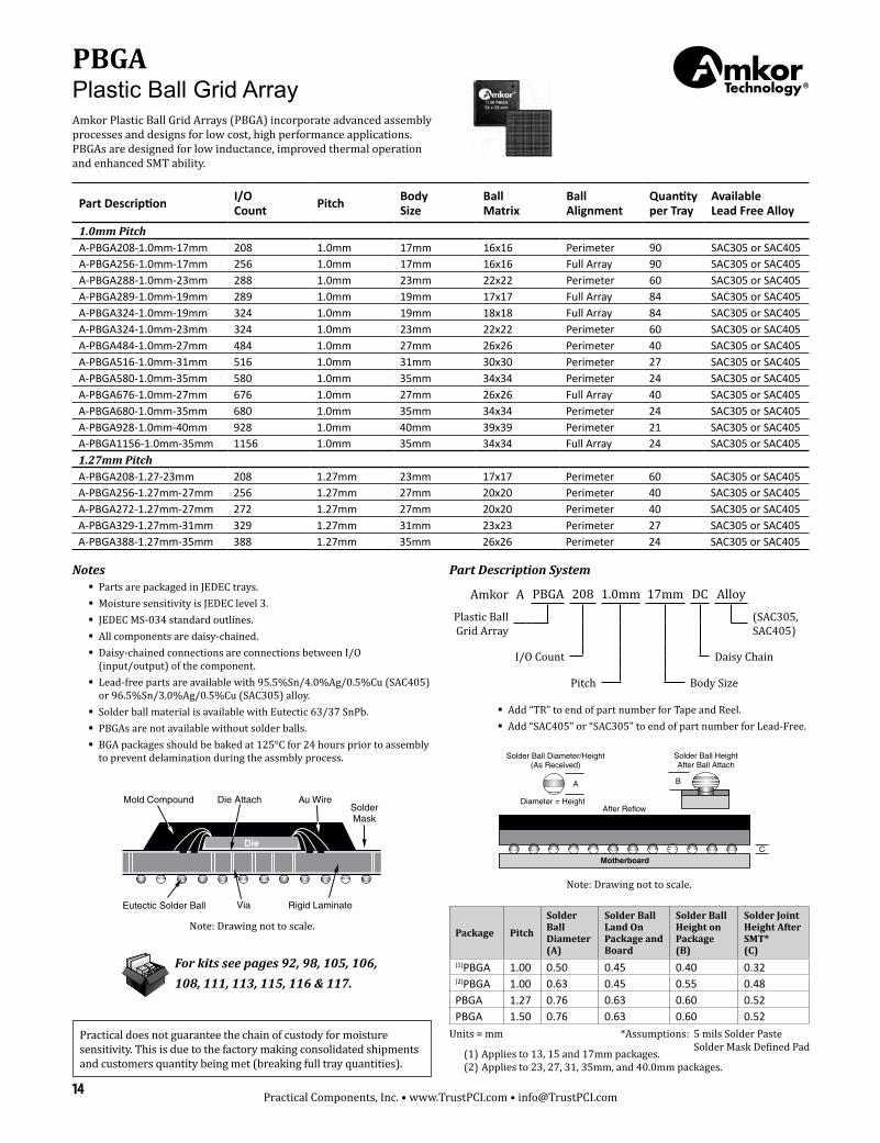
Notes � Parts are packaged in JEDEC trays. � Moisture sensitivity is JEDEC level 3. � JEDEC MS-034 standard outlines. � All components are daisy-chained. � Daisy-chained connections are connections between I/O
(input/output) of the component. � Lead-free parts are available with 95.5%Sn/4.0%Ag/0.5%Cu (SAC405)
or 96.5%Sn/3.0%Ag/0.5%Cu (SAC305) alloy. � Solder ball material is available with Eutectic 63/37 SnPb. � PBGAs are not available without solder balls. � BGA packages should be baked at 125°C for 24 hours prior to assembly
to prevent delamination during the assmbly process.
PBGAPlastic Ball Grid ArrayAmkor Plastic Ball Grid Arrays (PBGA) incorporate advanced assembly processes and designs for low cost, high performance applications. PBGAs are designed for low inductance, improved thermal operation and enhanced SMT ability.
For kits see pages 92, 98, 105, 106,108, 111, 113, 115, 116 & 117.
� Add “TR” to end of part number for Tape and Reel. � Add “SAC405” or “SAC305” to end of part number for Lead-Free.
Part Description I/O Count Pitch Body
SizeBall Matrix
Ball Alignment
Quantity per Tray
Available Lead Free Alloy
1.0mm PitchA-PBGA208-1.0mm-17mm 208 1.0mm 17mm 16x16 Perimeter 90 SAC305 or SAC405A-PBGA256-1.0mm-17mm 256 1.0mm 17mm 16x16 Full Array 90 SAC305 or SAC405A-PBGA288-1.0mm-23mm 288 1.0mm 23mm 22x22 Perimeter 60 SAC305 or SAC405A-PBGA289-1.0mm-19mm 289 1.0mm 19mm 17x17 Full Array 84 SAC305 or SAC405A-PBGA324-1.0mm-19mm 324 1.0mm 19mm 18x18 Full Array 84 SAC305 or SAC405A-PBGA324-1.0mm-23mm 324 1.0mm 23mm 22x22 Perimeter 60 SAC305 or SAC405A-PBGA484-1.0mm-27mm 484 1.0mm 27mm 26x26 Perimeter 40 SAC305 or SAC405A-PBGA516-1.0mm-31mm 516 1.0mm 31mm 30x30 Perimeter 27 SAC305 or SAC405A-PBGA580-1.0mm-35mm 580 1.0mm 35mm 34x34 Perimeter 24 SAC305 or SAC405A-PBGA676-1.0mm-27mm 676 1.0mm 27mm 26x26 Full Array 40 SAC305 or SAC405A-PBGA680-1.0mm-35mm 680 1.0mm 35mm 34x34 Perimeter 24 SAC305 or SAC405A-PBGA928-1.0mm-40mm 928 1.0mm 40mm 39x39 Perimeter 21 SAC305 or SAC405A-PBGA1156-1.0mm-35mm 1156 1.0mm 35mm 34x34 Full Array 24 SAC305 or SAC4051.27mm PitchA-PBGA208-1.27-23mm 208 1.27mm 23mm 17x17 Perimeter 60 SAC305 or SAC405A-PBGA256-1.27mm-27mm 256 1.27mm 27mm 20x20 Perimeter 40 SAC305 or SAC405A-PBGA272-1.27mm-27mm 272 1.27mm 27mm 20x20 Perimeter 40 SAC305 or SAC405A-PBGA329-1.27mm-31mm 329 1.27mm 31mm 23x23 Perimeter 27 SAC305 or SAC405A-PBGA388-1.27mm-35mm 388 1.27mm 35mm 26x26 Perimeter 24 SAC305 or SAC405
Part Description System
Amkor A PBGA 208 1.0mm 17mm DC Alloy
Plastic Ball Grid Array
(SAC305, SAC405)
I/O Count Daisy Chain
Pitch Body Size
Mold Compound Die Attach Au Wire
Eutectic Solder Ball Via Rigid Laminate
Die
SolderMask
Motherboard
After ReflowDiameter = Height
Solder Ball Diameter/Height(As Received)
Solder Ball HeightAfter Ball Attach
A B
C
Note: Drawing not to scale.
Note: Drawing not to scale.
Practical does not guarantee the chain of custody for moisture sensitivity. This is due to the factory making consolidated shipments and customers quantity being met (breaking full tray quantities).
Package Pitch
Solder Ball Diameter (A)
Solder Ball Land On Package and Board
Solder Ball Height on Package (B)
Solder Joint Height After SMT* (C)
(1)PBGA 1.00 0.50 0.45 0.40 0.32(2)PBGA 1.00 0.63 0.45 0.55 0.48PBGA 1.27 0.76 0.63 0.60 0.52PBGA 1.50 0.76 0.63 0.60 0.52
Units = mm
(1) Applies to 13, 15 and 17mm packages.(2) Applies to 23, 27, 31, 35mm, and 40.0mm packages.
*Assumptions: 5 mils Solder Paste Solder Mask Defined Pad

15Practical Components, Inc. • Tel: 1-714-252-0010 • Fax: 1-714-252-0026
Looking for Lead-Free?This symbol indicates that lead-free parts are available!
Mounting SurfaceResin Dam (Part of Substrate)
Solder Balls
SubstrateDie
Wires
Copper Heat Spreader
Encapsulant
Copper Ring
All units in mm.Assumptions: 5 mils solder paste. Solder mask defined pad.
SuperBGA® (SBGA) package is a very low profile, high-power BGA. The IC is directly attached to an integrated copper heatsink. Since the IC and the I/O are on the same side, signal vias are eliminated.
Motherboard
After ReflowDiameter = Height
Solder Ball Diameter/Height(As Received)
Solder Ball HeightAfter Ball Attach
A B
C
Note: Drawing not to scale.
Package Pitch A B C
SBGA 1.27 .76 .62 .52
� Add “SAC405” or “SAC305” to end of part number for Lead-Free.
Notes � Parts are packaged in JEDEC trays. � Moisture resistant (JEDEC level 3) � JEDEC MO-192 standard outlines � All components are daisy-chained � Lead-free parts are available with (SAC405) 95.5% Sn/4.0% Ag/0.5%
Cu alloy or (SAC305) 96.5% Sn/3.0% Ag/0.5% Cu alloy � Solder ball material is available with Eutectic 63/37 SnPb � SBGAs are not available without solder balls. � BGA packages should be baked at 125°C for 24 hours prior to assembly
to prevent delamination during assembly process. � Parts can be baked and dry-packed. � Superior thermal performance. � Light weight � Low profile (1.4mm mounted) � Enhanced electrical performance > 1 GHz
SBGASuperBGA®
SBGA SuperBGA® 1.27mm Pitch
Part Description I/O Count Pitch Body
SizeBall Matrix
Ball Alignment
Quantity per Tray
Available Lead Free Alloy
A-SBGA304-1.27mm-31mm 304 1.27mm 31mm 23x23 Perimeter 27 SAC305 or SAC405 A-SBGA560-1.27mm-42.5mm 560 1.27mm 42.5mm 33x33 Perimeter 12 SAC305 or SAC405 A-SBGA600-1.27mm-45mm 600 1.27mm 45mm 35x35 Perimeter 12 SAC305 orSAC405
Part Description System
Amkor A SBGA 304 1.27mm 31mm DC Alloy
Super Ball® Grid Array
(SAC305, SAC405)
I/O Count Daisy Chain
Pitch Body Size
Practical Components is the exclusive distributor of Amkor Technology Mechanical Components.

16 Practical Components, Inc. • www.TrustPCI.com • [email protected]
Amkor laminate ChipArray® packages are available without solder balls upon special order. Packages available without solder balls include CABGA, CTBGA and CVBGA. The same standard daisy-chained substrate would be used based on open tooling.
LGA is another term used for parts without solder balls. The same BOM (bill of material) is used when parts are assembled. LGA parts are used to reduce package height, drop test performance in handheld applications, solder ball attach practice, socket insertion, P&P evaluation, reflow profiling, enhance thermal cycle reliability and other purposes.
LGA solder interconnect if formed solely by solder paste applied at board assembly because there are no solder balls attached to the LGA. This results in a lower stand-off height of approximately 0.06mm to 0.10mm, depending on solder paste volume and PCB geometry. Laminate substrate is solder mask defined. Standard ball pad finish is NiAu.
Application notes available for supporting technical data.
Notes � Body sizes range from 5mm ~ 17mm. � Available pitches are .4mm, .5mm, .8mm and 1.0mm. � Parts packaged in trays (standard). � Parts available on Tape and Reel upon special request.
Unmounted device profile (with balls on left, LGA on right)
0.6 mm1.10 mm–1.30 mm
0.80 mm–1.00 mm2.71 mm–3.20 mm
0.6 mm1.1 mm–1.30 mm
1.92 mm–2.20 mm
LGALand Grid Array
Part Description System (example when ordering)
Amkor A CABGA 100 .8mm 10mm DC LGAChipArray®
Ball Grid ArrayLand Grid Array (no solder balls)
I/O CountDaisy Chain
PitchBody Size
Land Grid Array

17Practical Components, Inc. • Tel: 1-714-252-0010 • Fax: 1-714-252-0026
Notes � Fine pitch 0.4mm bottom package footprints. � Stacked package heights of 1.2mm nominal (see Stack Up table on
following pages). � Package configurations compliant with JEDEC standards. � Moisture Resistance Testing is JEDEC Level 3 @ 260 °C. � Temp Cycle –55/+125 °C, 1000 cycles. � HAST 130 °C, 85% RH, 96 hours. � Temp/Humidity 85 °C/85%RH/1000 hours. � High Temp Storage 150 °C, 1000 hours. � Board level Thermal Cycle –40/+125 °C, 1000 cycles. � Parts packaged in JEDEC matrix trays. � PoPs are only available Pb-free (not Tin-Lead). Available alloys are:
(SAC105) 98.5%Sn/1.0%Ag/0.5%Cu Top Package and (SAC125Ni) 98.2%Sn/1.2%Ag/0.5%Cu/0.05%Ni bottom package.
� It is recommended that parts be pre-baked at 125 °C for 48 hrs before using parts regarding moisture concern.
� PoP’s are not available without solder balls.
For kit see page 21.
See drawings on the following pages (18–20) for additional technical data. Color coded version available on our website: www.TrustPCI.com
Ball Diameter
I/O Count Ball Diameter
200 0.33mm620 0.30mm
Please Note � Amkor supporting data is available on our website for: Board Level
Reliability (BLR), PoP application notes, PoP Stencil & Stacking paper for SMT Conditions.
� IMAPS and SMTA White Paper Articles for additional supporting data available on our website: www.TrustPCI.com.
After three years of development, Amkor has introduced the next generation PoP solution. This new technology is called Through Mold Via (TMV®). The new TMV® technology is used to create interconnect vias through the mold cap, it also provides a more stable bottom package that enables the use of thinner substrates with a larger die to package ratio. TMV® enabled POP can support single, stacked die for wirebond and FC designs.
TMV® technology enables next generation PoPs by:
� Removing bottlenecks for fine pitch memory interfaces
� Enhancing warpage control and bottom package thickness reduction
� Increasing die to package size ratios
� Supporting wirebond, flip chip, stacked die and passive integration
� Improving board level solder joint life
TMV® PoP Through Mold Via Package
Practical Components is the exclusive distributor of Amkor Technology Mechanical Components.
TMV® PoP—Mating Top and Bottom Daisy Chain Samples
Part Description I/O Count Pitch Body
SizeBall Matrix
Ball Alignment
Quantity per Tray
Available Lead Free Alloy
14mm Body SizeA-PoP200-.5mm-14mm 200 (top) .5mm 14mm 27x27 Perimeter 119 SAC105A-TMV620-.4mm-14mm 620 (bottom) .4mm 14mm 33x33 Perimeter 119 SAC125
Part Description System (example when ordering)
Amkor A TMV 620 .4mm 14mm DC AlloyThrough Mold Via
(SAC105, SAC125)
I/O CountDaisy Chain
PitchBody Size
� Add “TR” to end of part number for die on Tape and Reel. � Add “SAC105” or “SAC125” to end of part number for
Lead-Free.
Through Mold Via

18 Practical Components, Inc. • www.TrustPCI.com • [email protected]
14mm 620 TMV Bottom Package Design Dimensions
Body (a) Foot Print–top (b) Foot Print–bottom (c) Die (d)
14 x 14mm 0.50 pitch, 200 ball 27 matrix, 2 row
0.4 pitch, 620 BGA 33 matrix, 4 + 2 row
7.6 x 7.6mm
Daisy Chain 4 Net Design
Daisy chain netlist of TMV, Bottom package balls.
Daisy chain netlist of top side (Top FBGA to TMV pin memory interface).
Corner NC pads of top site package.
Bottom package: Package Stackable TMV.
* Color diagram of DC Net design available on our website.
TMV® PoP Through Mold Via Package
A3, A31
[H17 H18], [H19 H20]
[T8 U8], [V8 W8]
Daisy chain netlist of TMV corners only.
Foot print - top (b)
Foot print - bottom (c)
Package size (a)
Die size (d)

19Practical Components, Inc. • Tel: 1-714-252-0010 • Fax: 1-714-252-0026
TMV 620 (Bottom Package) Bottom Side Daisy Chain Nets
200 PoP (Top Package ONLY) Daisy Chain Netlist
Top side main DC net
Top PoP + TMV Daisy Chain Netlist
Bottom side of bottom package (top view through package) 14x14mm, 0.4 mm TMV620, 33x33 ball matrix.
Top side of bottom package (top view through package) 14x14mm, 0.5 mm PoP200, 27x27 ball matrix.
* Color diagram of DC Net design available on our website.
TMV 620 (Bottom Package) Top Side Daisy Chain Nets
1 2 3 4 5 6 7 8 9 10 11 12 1314 15 16 17 18 19 20 21 22 23 24 25 26 27
A
B
C
D
E
F
G
H
J
K
L
M
N
P
R
T
U
V
W
Y
AA
AB
AC
AD
AE
AF
AG
Top View
1 2 3 4 5 6 7 8 9 10 11 12 1314 15 16 17 18 19 20 21 22 23 24 25 26 27
A
B
C
D
E
F
G
H
J
K
L
M
N
P
R
T
U
V
W
Y
AA
AB
AC
AD
AE
AF
AG
Connected thru
bottom side
[T8 U8] , [V8 W8]
Connected thru
bottom side
[H17 H18] , [H19 H20]
Top View
Daisy chain pattern of TMV–Bottom BGAs
Top side 16 corner ball DC net
1 2 3 4 5 6 7 8 9 10 11 12 1314 15 16 17 18 19 20 21 22 23 24 25 26 27 28 29 30 31 32 33
A
B
C
D
E
F
G
H
J
K
L
M
N
P
R
T
U
V
W
Y
AA
AB
AC
AD
AE
AF
AG
AH
AJ
AK
AL
AM
AN
Top View
1 2 3 4 5 6 7 8 9 10 11 12 1314 15 16 17 18 19 20 21 22 23 24 25 26 27
A
B
C
D
E
F
G
H
J
K
L
M
N
P
R
T
U
V
W
Y
AA
AB
AC
AD
AE
AF
AG
Connected thru
bottom side
[T8 U8] , [V8 W8]
Connected thru
bottom side
[H17 H18] , [H19 H20]
Top View
Daisy chain pattern of TMV–Bottom BGAs corner 24 balls
Top side main DC net
Top side 16 corner ball DC net
Top side 16 corner ball DC net
Top side main DC net
TMV® PoP Through Mold Via Package

20 Practical Components, Inc. • www.TrustPCI.com • [email protected]
TMV® PoP Overall Stack Up Table
100μm core, 350μm mode cap (Laminate)Symbol Unit Min Nom Max ToleranceA1 (Ball, 0.4 pitch) mm 0.100 0.150 0.200 0.05A2 (4L laminate) mm 0.260 0.300 0.340 0.04A3 (Mold cap) mm 0.230 0.350 0.380 0.03Total Bottom Pkg Height mm 0.729 0.800 0.871B1 (package stand-off) mm 0.370 0.400 0.430 0.03B2 Subs mm 0.100 0.130 0.160 0.03B3 Mold mm 0.380 0.400 0.420 0.02B2 + B3 mm 0.494 0.530 0.566Overall PoP Stack Height mm 1.301 1.380 1.459
Test Board PWB Netlist Pattern for BLR Testing
Stacked view of 4 DC Nets for BLR testing
* Color diagram of DC Net design available on our website.
1 2 3 4 5 6 7 8 9 10 11 12 1314 15 16 17 18 19 20 21 22 23 24 25 26 27 28 29 30 31 32 33
A
B
C
D
E
F
G
H
J
K
L
M
N
P
R
T
U
V
W
Y
AA
AB
AC
AD
AE
AF
AG
AH
AJ
AK
AL
AM
AN
1-1 1-2
2-1
2-23-1 3-2
4-1
4-2
Top View
A1
B3
A3B1
A2
B2
1 2 3 4 5 6 7 8 9 10 11 12 1314 15 16 17 18 19 20 21 22 23 24 25 26 27 28 29 30 31 32 33
A
B
C
D
E
F
G
H
J
K
L
M
N
P
R
T
U
V
W
Y
AA
AB
AC
AD
AE
AF
AG
AH
AJ
AK
AL
AM
AN
1-1 1-2
2-1
2-23-1 3-2
4-1
4-2
Top View
PWB Pattern for Test Board design
PWB Pattern for Test Board design
TMV® PoP Through Mold Via Package

21Practical Components, Inc. • Tel: 1-714-252-0010 • Fax: 1-714-252-0026
Notes � Board size is 132 x 77mm, 8 layers, .039" thick,
no microvias. � Board material is IS-410 High Temp. 180Tg. � Standard board finish is OSP Entek CU-106A-HT. � 15 daisy-chain pad placements for 14x14 620
TMV® component. � Immersion Silver board finish is available upon special
request. MOQ may apply. � Gerber and X,Y Theta data included at no charge.
PCB250 14mm TMV Drop Test Board
Ordering Information � Order Number: 15110 (board only) � Order Number: 31557 A-PoP200-.5-14mm-DC-105 (top component only) � Order Number: 31558 A-TMV620-.4-14mm-DC-125 (bottom component only)
Practical Components new TMV® 14MM test board and kit is a basic drop test board designed for the new Amkor TMV® (Through Mold Via) components.
This test eight layer board is a 3x5 array with 15 components placements per board. The board is 132mm x 77mm in size, and 1.0mm thick. The standard surface finish is OSP. Our test vehicle is designed for the new TMV® 620 solder ball .4mm pitch bottom component and the PoP 200 solder ball .5mm top component. Both top and bottom components have a daisy chain pattern through the substrate of the part.
A daisy chain pattern also runs through the test board. The design allows for daisy chain 3 net design. Meaning both top and bottom components as well as the board can be tested individually or as a group. This kit allows the end user to test the integrity of their process applications for TMV® components.
TMV® 14mm Board & KitDrop Test Lead Free Kit
Practical Components is the exclusive distributor of Amkor Technology Mechanical Components.

22 Practical Components, Inc. • www.TrustPCI.com • [email protected]
Notes � Fine pitch 0.5mm bottom package footprints � Stacked package heights of 1.2mm to 1.6mm available in a
variety of configurations (see Stack Up table on following pages) � Wafer thinning / handling < 100 µm � Consistent product performance and reliability � Package configurations compliant with JEDEC standards � Moisture Resistance Testing is JEDEC Level 3 @ 260 °C � Temp Cycle –55/+125 °C, 1000 cycles � HAST 130 °C, 85% RH, 96 hours � Temp/Humidity 85 °C/85%RH/1000 hours � High Temp Storage 150 °C, 1000 hours � Board level Thermal Cycle –40/+125 °C, 1000 cycles � Parts packaged in JEDEC matrix trays � PoPs are only available Pb-free (not Tin-Lead). Available alloys are:
SAC305, SAC405, SAC105 and SAC125Ni*. � *SAC125Ni (98.25%Sn/1.2%Ag/0.5%Cu/0.05%Ni) is only available for
bottom packages. � It is recommended that parts be pre-baked at 125 °C for 48 hrs before
using parts regarding moisture concern. � PoPs are not available without solder balls.
Amkor is offering daisy chain samples of their award winning bottom Package Stackable Very Thin Fine Pitch BGA (PSvfBGA) and their top PoP optimized for Package on Package (PoP) requirements. PoP has become the solution of choice for an increasing number of mobile consumer applications for 3D integration of logic and memory devices.
Amkor’s PSvfBGA is a high density fine pitch BGA package supporting logic or ASIC devices including base band, application and image processors. PoP stacking allows the OEM greater device, supplier and time to market flexibility by sourcing the bottom and top devices from their preferred logic and memory suppliers and then stacking the devices in the PWB surface mount assembly flow. A wide range of leading wireless and mobile integrated device manufacturers are relying on Amkor’s technical and industry leadership in PoP.
For kits see pages 31 & 35.
See drawings on the following pages (23–34) for additional technical data. Color coded version available on our website: www.TrustPCI.com
Ball Diameter
I/O Count Ball Diameter
128 0.45mm152 0.45mm305 0.30mm353 0.30mm
Please Note � Amkor supporting data is available on our website for: Board Level
Reliability (BLR), PoP application notes, PoP Stencil & Stacking paper for SMT Conditions.
� IMAPS and SMTA White Paper Articles for additional supporting data available on our website:www.TrustPCI.com.
Stacked Package
PoPPackage on Package
PoP Package on Package—Mating Top and Bottom Daisy Chain Samples
Part Description I/O Count Pitch Body
SizeBall Matrix
Ball Alignment
Quantity per Tray
Available Lead Free Alloy
12mm Body SizeA-PoP128-.65mm-12mm 128 (top) .65mm 12mm 18x18 Perimeter 152 SAC105, SAC305 or SAC405A-MPoP128-.65mm-12mm 128 (middle) .65mm 12mm 18x18 Perimeter 152 SAC105
A-PSvfBGA305-.5mm-12mm 305 (bot-tom)
.65mm (top) -
.5mm (bottom) 12mm 23x23 Perimeter 152 SAC125, SAC305 or SAC405
14mm Body SizeA-PoP152-.65mm-14mm 152 (top) .65mm 14mm 21x21 Perimeter 119 SAC105, SAC305 or SAC405
A-PSvfBGA353-.5mm-14mm 353 (bot-tom)
.65mm (top) -
.5mm (bottom) 14mm 26x26 Perimeter 119 SAC125, SAC305 or SAC405
Part Description System
Amkor A PoP 305 .5mm 12mm DC AlloyPackage on
Package(SAC305, SAC405, SAC105 & SAC125)
I/O CountDaisy Chain
PitchBody Size
� Add “TR” to end of part number for die on Tape and Reel. � Add “SAC305” , “SAC405”, “SAC105 ” or “SAC125” to end
of part number for Lead-Free.
Practical Components is the exclusive distributor of Amkor Technology Mechanical Components.
Package on Package (PoP)

23Practical Components, Inc. • Tel: 1-714-252-0010 • Fax: 1-714-252-0026
For kits see pages 31 & 35.
Foot print - top (b)
Foot print - bottom (c)
Package size (a)0.27mm
Max die size (d)
12mm 305 PSvfBGA Bottom Package Design Dimensions
Body (a) Foot Print–top (b) Foot Print–bottom (c) Die (d) Bond Fingers Available
12 x 12mm 0.65 pitch, 128 ball 18 matrix, 2 row
0.5 pitch, 292 I/Os 23 matrix, 4 row + 12 NC + A1 ball 305 BGA
7.0 mm 332
PoP Daisy Chain 3 Net Design
Daisy chain netlist of PSvfBGA, Bottom package balls.
Daisy chain netlist of top side (Top PoP to PSvfBGA 12 corner balls reserved for NC or additional supplies as memory combinations may require).
Daisy chain netlist of top side (Top PoP to PSvfBGA 116 pin memory interface).
Bottom package called: Package Stackable very thin fine pitch BGA (PSvfBGA).
L20 M20L20 M20
M4 N4M4 N4
Package on Package (PoP) 12x12mm, 0.65mm to pitch Stacked Daisy Chain
* Color diagram of DC Net design available on our website.
Package on Package (PoP)12x12mm Stacked Daisy Chain

24 Practical Components, Inc. • www.TrustPCI.com • [email protected]
PSvfBGA 305 (Bottom Package) Daisy Chain Nets
Daisy chain pattern of PSvfBGA -Bottom BGAs
128 PoP (Top Package) Daisy Chain Netlist
Daisy chain pattern of Top package for 116I/O memory interface
PoP + PSvfBGA Daisy Chain Netlist
Daisy chain netlist of Top PoP and PSvfBGA.
A
B
C
D
E
F
G
H
J
K
L
M
N
P
R
T
U
V
Connected thrubottom side (A)
1 2 3 4 5 6 7 8 9 10 11 12 13 14 15 16 17 18
* Connected thrubottom side (B)
*
1 2 3 4 5 6 7 8 9 10 11 12 13 14 15 16 17 18 19 20 21 22 23
A
B
C
D
E
F
G
H
J
K
L
M
N
P
R
T
U
V
W
Y
AA
AB
AC
(A)(B)
Bottom side of bottom package (top view through package) 12x12mm, 0.5 mm PSvfBGA305, 23x23 ball matrix
Top side of bottom package Top package interface (top view) 0.65 mm pitch, 128 pads, 18x18 ball matrix
Daisy chain pattern of PSvfBGA—Top memory pads
Top side 12 corner ball DC net
Top oPP packa egBottom side (top view
through package)
12x12 mm, 0.65 mm pitch128 PoP
18x18 ball matrix2 rows
1 2 3 4 5 6 7 8 9 10 11 12 13 14 15 16 17 18
A
B
C
D
E
F
G
H
J
K
L
M
N
P
R
T
U
V
Top PoPstacked on PSvfBGA
(top view through package
1 2 3 4 5 6 7 8 9 10 11 12 13 14 15 16 17 18
A
B
C
D
E
F
G
H
J
K
L
M
N
P
R
T
U
V
Connected thrubottom side (A)
1 2 3 4 5 6 7 8 9 10 11 12 13 14 15 16 17 18
* Connected thrubottom side (B)
Daisy chain pattern for 12 corner balls (typically reserved as NC for applications with no underfill, or option to add additional I/O or memory supplies as required for high density combinations)
* Color diagram of DC Net design available on our website.
Package on Package (PoP)12x12mm Stacked Daisy Chain

25Practical Components, Inc. • Tel: 1-714-252-0010 • Fax: 1-714-252-0026
PoP Overall Stack Up Example
A2A1
B3B2
B1
PoP +PSvfBGA
Symbol Unit Min Max Nom
A1 (Ball, 0.5 pitch) mm 0.150 0.250 0.200A2 (4L laminate) mm 0.260 0.340 0.300B1 (Ball, 0.65 pitch) mm 0.270 0.330 0.300B2 (2L laminate) mm 0.180 0.240 0.210B3 (Mold cap) mm 0.420 0.480 0.450Overall Pkg Height mm 1.378 1.542 1.460
B2 and B3 may vary depending on top memory PoP (MCP) design rules. Overall Stack up to be finalized based on top PoP rules.
PWB Netlist Pattern for BLR Testing
Stacked view of 3 DC Nets for BLR testing
1 2 3 4 5 6 7 8 9 10 11 12 13 14 15 16 17 18 19 20 21 22 23
A
B
C
D
E
F
G
H
J
K
L
M
N
P
R
T
U
V
W
Y
AA
AB
AC
3-1
3-2
4-1
4-2
1-2
1-1
1 2 3 4 5 6 7 8 9 10 11 12 13 14 15 16 17 18 19 20 21 22 23
A
B
C
D
E
F
G
H
J
K
L
M
N
P
R
T
U
V
W
Y
AA
AB
AC
3-1
3-2
4-1
4-2
1-2
1-1
Black line: PWB pattern In: 1-1, 3-1, 4-1 Common: 1-2, 3-2, 4-2
Black line: PWB pattern In: 1-1, 3-1, 4-1 Common: 1-2, 3-2, 4-2
* Color diagram of DC Net design available on our website.
Package on Package (PoP)12x12mm Stacked Daisy Chain

26 Practical Components, Inc. • www.TrustPCI.com • [email protected]
Package on Package (PoP) 12x12mm, 0.65mm to pitch Stacked Daisy Chain—3 Package Stacking
L20 M20
M4 N4
L20 M20
M4 N4
PoP Daisy Chain 3 Net Design—2 Package Stack
PoP Daisy Chain 3 Net Design—3 Package Stack
Daisy Chain netlist of PSvfBGA, Bottom package balls
Daisy chain netlist of top side (Top FBGA to PSvfBGA 116 pin memory interface)
Bottom package called: Package Stackable very thin fine pitch BGA (PSvfBGA)
Daisy Chain netlist of PSvfBGA, Bottom package balls
Daisy chain netlist of middle/bottom side (middle of PSvfBGA to bottom of PSvfBGA 128 balls)
Daisy chain netlist of middle/top side (FBGA to middle PSvfBGA 128 balls)
Bottom/middle package called: Package Stackable very thin fine pitch BGA (PSvfBGA)
Package on Package (PoP)12x12mm – 3 Package Stacking

27Practical Components, Inc. • Tel: 1-714-252-0010 • Fax: 1-714-252-0026
A2A1
B3B2
B1
Symbol Unit Min Nom Max
A1 (Ball, 0.5 pitch) mm 0.180 0.230 0.280A2 (4L laminate) mm 0.260 0.300 0.340B1 (Ball, 0.65 pitch) mm 0.270 0.300 0.330B2 (2L laminate) mm 0.180 0.210 0.240B3 (Mold cap) mm 0.420 0.450 0.480Overall Pkg Height mm 1.408 1.490 1.572
PoP Overall Stack Up—2 Package Stack
Assumed standard DC substrate Thinner stack up feasible in future build
A2A1
C1
C3C2
B2B1
PoP Overall Stack Up—3 Package Stack
Symbol Unit Min Nom Max
A1 (Ball, 0.5 pitch) mm 0.180 0.230 0.280A2 (4L laminate) mm 0.260 0.300 0.340B1 (Ball, 0.65 pitch) mm 0.270 0.300 0.330B2 (2L laminate) mm 0.180 0.210 0.240C1 (Ball, 0.65 pitch) mm 0.270 0.300 0.330C2 (2L laminate) mm 0.180 0.210 0.240C3 (Mold cap) mm 0.420 0.450 0.480Overall Pkg Height mm 1.907 2.000 2.093
Assumed standard DC substrate Thinner stack up feasible in future build
Package on Package (PoP)12x12mm – 3 Package Stacking

28 Practical Components, Inc. • www.TrustPCI.com • [email protected]
Connected tobottom side (C)
1 2 3 4 5 6 7 8 9 10 11 12 13 14 15 16 17 18
A
B
C
D
E
F
G
H
J
K
L
M
N
P
R
T
U
V
Top View
1 2 3 4 5 6 7 8 9 10 11 12 13 14 15 16 17 18
A
B
C
D
E
F
G
H
J
K
L
M
N
P
R
T
U
V
(C)
PSvfBGA 305 (Bottom Package) Daisy Chain Nets
Bottom side of bottom package (top view through package) 12x12mm, 0.65 mm PSvfBGA305, 23x23 ball matrix
Top side of bottom package Top/Middle package interface (top view) 0.65mm pitch, 128 pads, 18x18 ball matrix
1 2 3 4 5 6 7 8 9 10 11 12 13 14 15 16 17 18 19 20 21 22 23
A
B
C
D
E
F
G
H
J
K
L
M
N
P
R
T
U
V
W
Y
AA
AB
AC
(A)(B)
Connected tobottom side (A)
1 2 3 4 5 6 7 8 9 10 11 12 13 14 15 16 17 18
A
B
C
D
E
F
G
H
J
K
L
M
N
P
R
T
U
V
* Connected tobottom side (B)
*
Top View
Top side 12 corner ball DC netDaisy chain pattern of PSvfBGA—Bottom BGAsDaisy chain pattern of PSvfBGA—Top memory pads
Bottom side of middle package (top view through package) 12x12mm, 0.65 mm PSvfBGA128, 18x18 ball matrix
Top side of middle package Top package interface (top view) 0.65mm pitch, 128 pads, 18x18 ball matrix
PSvfBGA 128 (Middle Package) Daisy Chain Nets
Each pad on the top side is connected to the corresponding pad on the bottom side through via.
Package on Package (PoP)12x12mm – 3 Package Stacking

29Practical Components, Inc. • Tel: 1-714-252-0010 • Fax: 1-714-252-0026
1 2 3 4 5 6 7 8 9 10 11 12 13 14 15 16 17 18
A
B
C
D
E
F
G
H
J
K
L
M
N
P
R
T
U
V
Connected thrubottom side (A)
* Connected thrubottom side (B)
Top FBGA packageBottom side (top view
through package)
12x12 mm, 0.65 mm pitchFBGA 128
18x18 ball matrix2 rows
1 2 3 4 5 6 7 8 9 10 11 12 13 14 15 16 17 18
A
B
C
D
E
F
G
H
J
K
L
M
N
P
R
T
U
V
Top View
FBGA 128 (Top Package) Daisy Chain Netlist
Middle-to-Bottom Package Connection after 3 PKG Stack
Daisy chain pattern of Top package for 116 I/O memory interface
Top View
Package on Package (PoP)12x12mm – 3 Package Stacking

30 Practical Components, Inc. • www.TrustPCI.com • [email protected]
1 2 3 4 5 6 7 8 9 10 11 12 13 14 15 16 17 18 19 20 21 22 23
A
B
C
D
E
F
G
H
J
K
L
M
N
P
R
T
U
V
W
Y
AA
AB
AC
3-1
3-2
4-1
4-2
1-2
1-1
1 2 3 4 5 6 7 8 9 10 11 12 13 14 15 16 17 18 19 20 21 22 23
A
B
C
D
E
F
G
H
J
K
L
M
N
P
R
T
U
V
W
Y
AA
AB
AC
3-1
3-2
4-1
4-2
1-2
1-1
PWB Netlist Pattern for BLR Testing Stacked View of 3 DC Nets for BLR Testing
Top View Top View Top View Top View
PWB Pattern In: 1-1, 3-1, 4-1 Common: 1-2, 3-2, 4-2
PWB Pattern In: 1-1, 3-1, 4-1 Common: 1-2, 3-2, 4-2
Top View
1 2 3 4 5 6 7 8 9 10 11 12 13 14 15 16 17 18
A
B
C
D
E
F
G
H
J
K
L
M
N
P
R
T
U
V
Connected tobottom side (A)
Top-to-Middle Package Connection after 3 PKG Stack
Package on Package (PoP)12x12mm – 3 Package Stacking

31Practical Components, Inc. • Tel: 1-714-252-0010 • Fax: 1-714-252-0026
This PoP 12mm Board and Kit is designed as test vehicle for the new Amkor (PSvfBGA) 12x12 305 PoP package. PoP packages from Amkor focus on high density logic devices.
PoP packages are designed for products such as cell phones, digital cameras and other mobile applications benefiting from the combination of stacked packages and small footprint technology. This test board enables the end user to test their process applications on the top and bottom PoP components.
With daisy-chain patterns in both packages and the PCB200 Board, customers are able to check for continuity to guarantee the integrity of their process.
PCB200 12mm Board
Order Notes � Order Number: 19577 PCB200 12mm (board only) � Order Number: 31288 A-PoP128-.65mm-12mm-DC-SAC105 (top component only) � Order Number: 31289 A-PSvfBGA305-.5mm-12mm-DC-SAC125Ni (bottom component only)
Notes � Board size is 132 x 77mm, 8-layers, .039" thick,
no microvias. � Board material is IS-410 High Temp 180Tg. � Standard board finish OSP Entek CU-106A-HT. � Immersion Silver finish is also available upon special
request. MOQ may apply. � 15 daisy-chain pad placements for 12x12
305 PoP component. � Gerber and X,Y Theta data included at no charge. � See page 22 for available solder ball alloy’s for PoP
components. SAC305, SAC405, SAC105 and SAC125Ni is available.
PoP 12mm Board and KitLead-Free Test Kit
Practical Components is the exclusive distributor of Amkor Technology Mechanical Components.

32 Practical Components, Inc. • www.TrustPCI.com • [email protected]
Foot print - top (b)
Foot print - bottom (c)
Package size (a)0.27mm
Max die size (d)
Body (a) Foot Print–top (b) Foot Print–bottom (c) Die (d) Bond Fingers Available
14 x14 mm 0.65 pitch, 152 ball 21 matrix, 2 row
0.5 pitch, 340 I/Os 26 matrix, 4 row + 12 NC + A1 ball 353 BGA
8.9 mm 328 to 396
14mm 353 PSvfBGA Bottom Package Design Dimensions
PoP Daisy Chain 3 Net Design
M23 N23
M4 N4M4 N4
Daisy chain netlist of PSvfBGA, Bottom package balls
Daisy chain netlist of top side (Top PoP to PSvfBGA 140 pin memory interface)
Daisy chain netlist of top side (Top PoP to PSvfBGA 12 corner balls reserved for NC or additional supplies as memory combinations may require).
Bottom package called: Package Stackable very thin fine pitch BGA (PSvfBGA)
Package on Package (POP) 14x14mm Stacked Daisy Chain
* Color diagram of DC Net design available on our website.
Package on Package (PoP)14x14mm Stacked Daisy Chain

33Practical Components, Inc. • Tel: 1-714-252-0010 • Fax: 1-714-252-0026
1 2 3 4 5 6 7 8 9 10 11 12 13 14 15 16 17 18 19 20 21 22 23 24 25 26
A
B
C
D
E
F
G
H
J
K
L
M
N
P
R
T
U
V
W
Y
AA
AB
AC
AD
AE
AF
(A) (B) Connected withbottom side (A)
1 2 3 4 5 6 7 8 9 10 11 12 13 14 15 16 17 18 19 20 21
A
B
C
D
E
F
G
H
J
K
L
M
N
P
R
T
U
V
W
Y
AA
Connected thrubottom side (B)
1 2 3 4 5 6 7 8 9 10 11 12 13 14 15 16 17 18 19 20 21 22 23 24 25 26
A
B
C
D
E
F
G
H
J
K
L
M
N
P
R
T
U
V
W
Y
AA
AB
AC
AD
AE
AF
(A) (B) Connected withbottom side (A)
1 2 3 4 5 6 7 8 9 10 11 12 13 14 15 16 17 18 19 20 21
A
B
C
D
E
F
G
H
J
K
L
M
N
P
R
T
U
V
W
Y
AA
Connected thrubottom side (B)
PSvfBGA 353 (Bottom Package) Daisy Chain Nets
Daisy chain pattern of PSvfBGA—Bottom BGAs
Daisy chain pattern of PSvfBGA—Top
memory pads Top side 12 corner ball DC net
Top side 12 corner ball DC net
Top side 12 corner ball DC net
Top PoPstacked on PSvfBGA
(top view through package)
1 2 3 4 5 6 7 8 9 10 11 12 13 14 15 16 17 18 19 20 21
A
B
C
D
E
F
G
H
J
K
L
M
N
P
R
T
U
V
W
Y
AA
Connected withbottom side (A)
Connected withbottom side (B)
Top PoP + PSvfBGA Daisy Chain Netlist
Daisy chain netlist of Top FBGA and PSvfBGA
Bottom side (top view through package) 14x14mm, 0.5 mm PSvfBGA353, 26x26 ball matrix
Top side —Top package interface (top view) 0.65 mm pitch, 152 pads, 21x21 ball matrix
Top PoP packageBottom side (top view
through package)
14x14 mm, 0.65 mm 152 PoP21x21 ball matrix
2 tiers
1 2 3 4 5 6 7 8 9 10 11 12 13 14 15 16 17 18 19 20 21
A
B
C
D
E
F
G
H
J
K
L
M
N
P
R
T
U
V
W
Y
AA
152 PoP (Top Package) Daisy Chain Netlist
Daisy chain pattern of Top package for 140 I/O memory interface
Daisy chain pattern for 12 corner balls (typically reserved as NC for applications with no underfill, or option to add additional I/O or memory supplies as required for high density combinations).
* Color diagram of DC Net design available on our website.
Package on Package (PoP)14x14mm Stacked Daisy Chain

34 Practical Components, Inc. • www.TrustPCI.com • [email protected]
PWB Netlist Pattern for BLR Testing
Stacked View of 3 DC Nets For BLR Testing
PoP Overall Stack Up Example
A2A1
B3B2
B1
PoP + PSvfBGA
Symbol Unit Min Max Nom
A1 (Ball, 0.5 pitch) mm 0.150 0.250 0.200A2 (4L laminate) mm 0.260 0.340 0.300B1 (Ball, 0.65 pitch) mm 0.270 0.330 0.300B2 (2L laminate) mm 0.180 0.240 0.210B3 (Mold cap) mm 0.420 0.480 0.450Overall Package Height mm 1.378 1.542 1.460
B2 and B3 may vary depending on top memory PoP (MCP) design rules. Overall Stack up to be finalized based on top PoP rules.
1 2 3 4 5 6 7 8 9 10 11 12 13 14 15 16 17 18 19 20 21 22 23 24 25 26
A
B
C
D
E
F
G
H
J
K
L
M
N
P
R
T
U
V
W
Y
AA
AB
AC
AD
AE
AF
1-2
1-1
3-1
3-2
4-1
4-2
PWB (top view)
Black line: PWB pattern In: 1-1, 3-1, 4-1 Common: 1-2, 3-2, 4-2
Black line: PWB pattern In: 1-1, 3-1, 4-1 Common: 1-2, 3-2, 4-2
* Color diagram of DC Net design available on our website.
1 2 3 4 5 6 7 8 9 10 11 12 13 14 15 16 17 18 19 20 21 22 23 24 25 26
A
B
C
D
E
F
G
H
J
K
L
M
N
P
R
T
U
V
W
Y
AA
AB
AC
AD
AE
AF
1-2
1-1
3-1
3-2
4-1
4-2
Package on Package (PoP)14x14mm Stacked Daisy Chain

35Practical Components, Inc. • Tel: 1-714-252-0010 • Fax: 1-714-252-0026
This PoP 14mm Board and Kit is designed as test vehicle for the new Amkor (PSvfBGA) 14x14 305 PoP package. PoP packages from Amkor focus on high density logic devices.
PoP packages are designed for products such as cell phones, digital cameras and other mobile applications benefiting from the combination of stacked packages and small footprint technology. This test board enables the end user to test their process applications on the top and bottom PoP components.
With daisy-chain patterns in both packages and the PCB200 Board, customers are able to check for continuity to guarantee the integrity of their process.
PCB200 14mm Board
Ordering Information � Order Number: 12953 PCB200-14mm-OSPHT (board only) � Order Number: 31290 A-PoP152-.65mm-14mm-DC-LF-SAC105 (top component only) � Order Number: 31291 A-PSvfBGA353-.5mm-14mm-DC-LF-SAC125Ni (bottom component only)
Notes � Board size is 132 x 77mm, 8-layers, .039" thick,
no microvias. � Board material is IS-410 High Temp 180Tg. � Standard board finish OSP Entek CU-106A-HT. � 15 daisy-chain pad placements for 14x14
353 PSvfPGA component. � Immersion Silver finish is also available upon special
request. MOQ may apply. � Gerber and X,Y Theta data included at no charge. � See page 22 for available solder ball alloy’s for PoP
components. SAC305, SAC405, SAC105 and SAC125Ni is available.
PoP 14mm Board & KitLead-Free Test Kit
Practical Components is the exclusive distributor of Amkor Technology Mechanical Components.

36 Practical Components, Inc. • www.TrustPCI.com • [email protected]
OmQFNOpen-molded Quad Flat Pack No Leads
From prototype to production volumes, these pre-molded QFN packages, created by Quik-Pak, provide a high quality, fast solution for your assembly needs.
The pre-molded packages come in a variety of sizes. They are available from 3x3mm to 12x12mm body size with lead pitch sizes ranging from .8mm to .4mm. Covers or lids are also available for air cavity applications.
Notes � Larger die paddle area. � Supports larger die and ground bonds per given body size. � RoHS and REACH compliant “green” molding compound. � Gold plated. � Superior bondability. � Custom body sizes and lead counts available. � Components can be encapsulated or lids are available. � 40Au/80Ni Plated
Assembly Solutions Include the following: � Wafer Dicing � Wire Bonding � Custom Packaging � Backgrinding � Complete Assembly
OmQFN Open-molded Quad Flat Pack No Leads Package
Part Description Lead Count Body Size Pitch
.4mm PitchQPQFN28-4mm-.4mm 28 4mm .4mmQPQFN48-6mm-.4mm 48 6mm .4mmQPQFN88-10mm-.4mm 88 10mm .4mmQPQFN100-12mm-.4mm 100 12mm .4mm.5mm PitchQPQFN12-3mm-.5mm 12 3mm .5mmQPQFN16-3mm-.5mm 16 3mm .5mmQPQFN20-4mm-.5mm 20 4mm .5mmQPQFN24-4mm-.5mm 24 4mm .5mmQPQFN28-5mm-.5mm 28 5mm .5mmQPQFN32-5mm-.5mm 32 5mm .5mmQPQFN40-6mm-.5mm 40 6mm .5mmQPQFN44-7mm-.5mm 44 7mm .5mmQPQFN48-7mm-.5mm 48 7mm .5mmQPQFN56-8mm-.5mm 56 8mm .5mmQPQFN64-9mm-.5mm 64 9mm .5mmQPQFN72-10mm-.5mm 72 10mm .5mmQPQFN80-12mm-.5mm 80 12mm .5mm.65mm PitchA-MLF8-3mm-.65mm 8 3mm .65mmQPQFN12-3mm-.65mm 12 3mm .65mmQPQFN16-4mm-.65mm 16 4mm .65mmQPQFN20-5mm-.65mm 20 5mm .65mmQPQFN24-5mm-.65mm 24 5mm .65mmQPQFN28-6mm-.65mm 28 6mm .65mmQPQFN32-7mm-.65mm 32 7mm .65mm
Part Description System QP QFN 28 4mm .4mm
Quik-Pak PitchQuad Flat Pack
No Leads Body Size
Lead Count
OmQFN
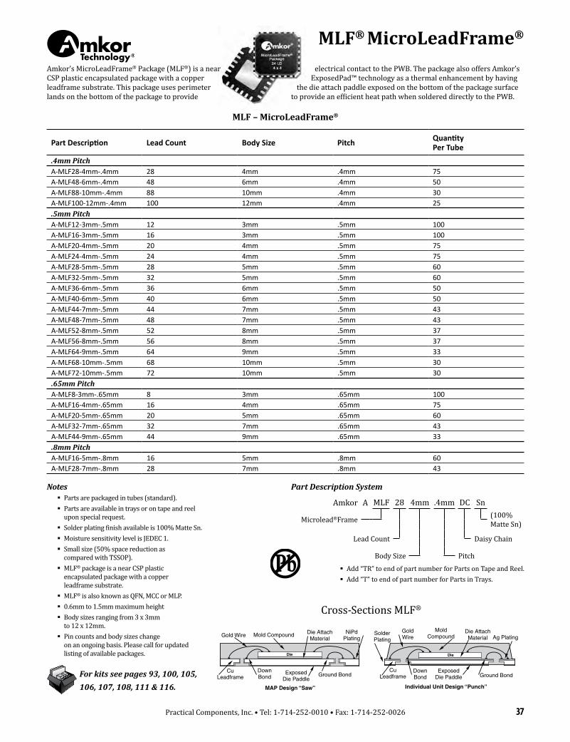
37Practical Components, Inc. • Tel: 1-714-252-0010 • Fax: 1-714-252-0026
Amkor’s MicroLeadFrame® Package (MLF®) is a near CSP plastic encapsulated package with a copper leadframe substrate. This package uses perimeter lands on the bottom of the package to provide
electrical contact to the PWB. The package also offers Amkor’s ExposedPad™ technology as a thermal enhancement by having
the die attach paddle exposed on the bottom of the package surface to provide an efficient heat path when soldered directly to the PWB.
Notes � Parts are packaged in tubes (standard). � Parts are available in trays or on tape and reel
upon special request. � Solder plating finish available is 100% Matte Sn. � Moisture sensitivity level is JEDEC 1. � Small size (50% space reduction as
compared with TSSOP). � MLF® package is a near CSP plastic
encapsulated package with a copper leadframe substrate.
� MLF® is also known as QFN, MCC or MLP. � 0.6mm to 1.5mm maximum height � Body sizes ranging from 3 x 3mm
to 12 x 12mm. � Pin counts and body sizes change
on an ongoing basis. Please call for updated listing of available packages. Die
Gold Wire Mold Compound Die AttachMaterial
NiPdPlating
Ground BondCu
LeadframeDownBond
ExposedDie Paddle
MAP Design “Saw”
Die
Ag PlatingDie AttachMaterial
MoldCompound
GoldWire
SolderPlating
CuLeadframe
DownBond Ground Bond
ExposedDie Paddle
Individual Unit Design “Punch”
Cross-Sections MLF®
For kits see pages 93, 100, 105,106, 107, 108, 111 & 116.
MLF® MicroLeadFrame®
MLF – MicroLeadFrame®
Part Description Lead Count Body Size Pitch Quantity Per Tube
.4mm PitchA-MLF28-4mm-.4mm 28 4mm .4mm 75A-MLF48-6mm-.4mm 48 6mm .4mm 50A-MLF88-10mm-.4mm 88 10mm .4mm 30A-MLF100-12mm-.4mm 100 12mm .4mm 25.5mm PitchA-MLF12-3mm-.5mm 12 3mm .5mm 100A-MLF16-3mm-.5mm 16 3mm .5mm 100A-MLF20-4mm-.5mm 20 4mm .5mm 75A-MLF24-4mm-.5mm 24 4mm .5mm 75A-MLF28-5mm-.5mm 28 5mm .5mm 60A-MLF32-5mm-.5mm 32 5mm .5mm 60A-MLF36-6mm-.5mm 36 6mm .5mm 50A-MLF40-6mm-.5mm 40 6mm .5mm 50A-MLF44-7mm-.5mm 44 7mm .5mm 43A-MLF48-7mm-.5mm 48 7mm .5mm 43A-MLF52-8mm-.5mm 52 8mm .5mm 37A-MLF56-8mm-.5mm 56 8mm .5mm 37A-MLF64-9mm-.5mm 64 9mm .5mm 33A-MLF68-10mm-.5mm 68 10mm .5mm 30A-MLF72-10mm-.5mm 72 10mm .5mm 30.65mm PitchA-MLF8-3mm-.65mm 8 3mm .65mm 100A-MLF16-4mm-.65mm 16 4mm .65mm 75A-MLF20-5mm-.65mm 20 5mm .65mm 60A-MLF32-7mm-.65mm 32 7mm .65mm 43A-MLF44-9mm-.65mm 44 9mm .65mm 33.8mm PitchA-MLF16-5mm-.8mm 16 5mm .8mm 60A-MLF28-7mm-.8mm 28 7mm .8mm 43
Part Description System
Amkor A MLF 28 4mm .4mm DC Sn
Microlead®Frame (100% Matte Sn)
Lead Count Daisy Chain
Body Size Pitch � Add “TR” to end of part number for Parts on Tape and Reel. � Add “T” to end of part number for Parts in Trays.
MicroLead Frame

38 Practical Components, Inc. • www.TrustPCI.com • [email protected]
Amkor’s new Dual Row MLF® (MicroLeadFrame®) package with 2 rows of lands is a cost effective, high performance solution for devices requiring up to 164 I/O. Typical applications include hard disk drives, USB controllers, and Wireless LAN. The small size and weight, along with excellent thermal and electrical performance, make the MLF® package an ideal choice for handheld portable applications such as cell phones and PDAs or any other application where size, weight and package performance are required issues.
Notes � Parts are packaged in tubes (standard). � Parts are available in trays or on tape and reel upon special request. � Solder plating finish available is 100% Matte Sn. � Moisture sensitivity level is JEDEC 1. � Small size (reduce package footprint by 50% or more and improved
RF performance) and weight. � Process flow is same as standard “punch” MLF®. � Dual row MLF® offers enhanced thermal capability. � SnPb parts no longer available.
MQFP3.93 mm
SOICCABGA
SOT/SC
LQFPTSOP1.6mm
TSOPTQFP
1.2 mmTSSOP1.1 mm
MLF0.9 mm
0.8 mm0.6 mm
MQFP2.33 mm
� Add “TR” to end of part number for Tape and Reel. � Add “T” to end of part number for parts in Trays.
For kits see pages 108 & 111.
Dual Row MLF®
Part Description Lead Count Body Size Pitch Quantity Per Tube
.5mm PitchA-DualRowMLF156-12mm-.5mm 156 12mm .5mm 25
Part Description System
Amkor A DualRowMLF 156 12mm .5mm DC Sn
Dual Row MicroLeadFrame®
(100% Matte Sn)
Lead Count Daisy Chain
Body Size Pitch
Practical Components is the exclusive distributor of Amkor Technology Mechanical Components.
Package Height Comparison

39Practical Components, Inc. • Tel: 1-714-252-0010 • Fax: 1-714-252-0026
Thin Quad Flat Pack (TQFP) packages provide the same benefit of the metric QFP package, but are thinner (body thickness of 1.0mm) and have a standard lead-frame footprint (2.0mm lead footprint). TQFPs are helping to solve issues such as increasing board density, die shrink programs, thin end-product profile and portability. Lead counts range from 32 to 176. Body sizes range from 5 x 5mm to 20 x 20mm. Copper lead-frames are used for the TQFP package.
Exposed Pad L/TQFP Package
Notes � All TQFP are standard in trays. � Parts available on Tape and Reel. � TQFP have body thickness of 1.0mm. � Moisture sensitivity is JEDEC level 3. � Lead-free parts are available with 100% Matte Sn finish. � SnPb parts no longer available.
� Add “TR” to end of part number for Tape and Reel. � Add “SN” to end of part number for Lead-Free parts.
Au Wire
MoldCompoundCu Leadframe
Exposed Pad Die Attach
Die Up (Standard)
Die
TQFPThin Quad Flat Pack
TQFP Thin Quad Flat Pack 1.0mm Thick
Part Description Number of Pins
Body Size
Lead Pitch
Quantity Per Tray
Tape Width
Tape Pitch
Quantity Per Reel
.4mm PitchA-TQFP40-5mm-.4mm-2.0 40 5mm sq .4mm 360 16mm 12mm 1,000A-TQFP64-7mm-.4mm-2.0 64 7mm sq .4mm 250 16mm 12mm 1,000A-TQFP120-14mm-.4mm-2.0 120 14mm sq .4mm 90 32mm 24mm 750A-TQFP128-14mm-.4mm-2.0 128 14mm sq .4mm 90 32mm 24mm 750A-TQFP176-20mm-.4mm-2.0 176 20mm sq .4mm 60 44mm 24mm 500.5mm PitchA-TQFP32-5mm-.5mm-2.0 32 5mm sq .5mm 360 16mm 12mm 1,000A-TQFP48-7mm-.5mm-2.0 48 7mm sq .5mm 250 16mm 12mm 1,000A-TQFP64-10mm-.5mm-2.0 64 10mm sq .5mm 160 24mm 16mm 1,000A-TQFP80-12mm-.5mm-2.0 80 12mm sq .5mm 119 24mm 24mm 1,000A-TQFP100-14mm-.5mm-2.0 100 14mm sq .5mm 90 32mm 24mm 750A-TQFP128-20mm-.5mm-2.0 128 20mm sq .5mm 60 44mm 24mm 500A-TQFP144-20mm-.5mm-2.0 144 20mm sq .5mm 60 44mm 24mm 500.65mm PitchA-TQFP80-14mm-.65mm-2.0 80 14mm sq .65mm 90 32mm 24mm 750.8mm PitchA-TQFP32-7mm-.8mm-2.0 32 7mm sq .8mm 250 16mm 12mm 1,000A-TQFP44-10mm-.8mm-2.0 44 10mm sq .8mm 160 24mm 16mm 1,000A-TQFP52-10mm-.8mm-2.0 52 10mm sq .8mm 160 24mm 16mm 1,000A-TQFP64-14mm-.8mm-2.0 64 14mm sq .8mm 90 32mm 24mm 750
Part Description System
Amkor A TQFP 40 5mm .4mm 2.0 DC Sn
Thin Quad Flat Pack (100% Matte Sn)
Number of Pins Daisy ChainBody Size Lead Footprint
Lead PitchTQFP Package
Au Wire
MoldCompound
Cu Leadframe
Die Attach Pad
Die Up (Standard)
Die 1.0mm
Die AttachAdhesive
Au Wire
Die Attach
Cu Leadframe
Exposed Pad MoldCompound
Die
Die Down (Inverted)
Quad Flat Packs

40 Practical Components, Inc. • www.TrustPCI.com • [email protected]
Low Profile Quad Flat Pack (LQFP) packages provide the same benefit of the metric QFP packages, but are thinner (body thickness of 1.4mm) and have a standard lead-frame footprint (2.0mm lead footprint).
LQFPs help to solve issues such as increasing board density, die shrink programs, thin end-product profile and portability. Lead counts range from 32 to 256. Body sizes range from 7 x 7mm to 28 x 28mm. Copper lead-frames are used for the LQFP package.
For kits see pages 100, 101, 105, 108,111, 116 & 117.
� Add “TR” to end of part number for Tape and Reel. � Add “SN” to end of part number for Lead Free parts.
Daisy-Chain Parts Available!
For drawings, please visit our web site at www.TrustPCI.com.
Notes � All LQFPs are standard in trays. � Parts available on Tape and Reel. � LQFPs have a body thickness of 1.4mm. � Moisture sensitivity is JEDEC level 3. � Lead-free parts are available with 100% Matte Sn finish. � SnPb parts no longer available.
LQFPLow Profile Quad Flat Pack
Part Description System
Amkor A LQFP 64 7mm .4mm 2.0 DC Sn
Low Profile Quad Pack
(100% Matte Sn)
Number of Pins Daisy ChainBody Size Lead Footprint
Lead Pitch
LQFP Low Profile Quad Flat Pack 1.4mm Thick
Part Description Number of Pins
Body Size
Lead Pitch
Quantity Per Tray
Tape Width
Tape Pitch
Quantity Per Reel
.4mm PitchA-LQFP64-7mm-.4mm-2.0 64 17mm sq .4mm 250 16mm 12mm 1,000A-LQFP120-14mm-.4mm-2.0 120 14mm sq .4mm 90 32mm 24mm 750A-LQFP128-14mm-.4mm-2.0 128 14mm sq .4mm 90 32mm 24mm 750A-LQFP176-20mm-.4mm-2.0 176 20mm sq .4mm 60 44mm 24mm 500A-LQFP216-24mm-.4mm-2.0 216 24mm sq .4mm 40 44mm 32mm 500A-LQFP256-28mm-.4mm-2.0 256 28mm sq .4mm 36 44mm 40mm 500.5mm PitchA-LQFP48-7mm-.5mm-2.0 48 7mm sq .5mm 250 16mm 12mm 1,000A-LQFP64-10mm-.5mm-2.0 64 10mm sq .5mm 160 24mm 24mm 1,000A-LQFP100-14mm-.5mm-2.0 100 14mm sq .5mm 90 32mm 24mm 750A-LQFP128-14x20-.5mm-2.0 128 14x20mm .5mm 72 44mm 32mm 500A-LQFP128-20mm-.5mm-2.0 128 20mm sq .5mm 60 44mm 24mm 500A-LQFP144-20mm-.5mm-2.0 144 20mm sq .5mm 60 44mm 24mm 750A-LQFP160-24mm-.5mm-2.0 160 24mm sq .5mm 40 44mm 32mm 500A-LQFP176-24mm-.5mm-2.0 176 24mm sq .5mm 40 44mm 32mm 500A-LQFP208-28mm-.5mm-2.0 208 28mm sq .5mm 36 44mm 40mm 500.65mm PitchA-LQFP52-10mm-.65mm-2.0 52 10mm sq .65mm 160 24mm 24mm 1,000A-LQFP80-14mm-.65mm-2.0 80 14mm sq .65mm 90 32mm 24mm 750A-LQFP100-14x20-.65mm-2.0 100 14x20mm .65mm 72 44mm 32mm 500.8mm PitchA-LQFP32-7mm-.8mm-2.0 32 7mm sq .8mm 250 16mm 12mm 1,000A-LQFP44-10mm-.8mm-2.0 44 10mm sq .8mm 160 24mm 24mm 1,000A-LQFP64-14mm-.8mm-2.0 64 14mm sq .8mm 90 32mm 24mm 750

41Practical Components, Inc. • Tel: 1-714-252-0010 • Fax: 1-714-252-0026
Notes � All QFPs are standard in JEDEC trays. � Tray quantities may vary. � Parts available on Tape and Reel. � Lead-free parts are available with 100% Matte Sn finish.
Quad Flat Pack (QFP) components have four sides with leads extending from the component body on all four sides. QFP components come packaged in trays or on tape and reel to protect the component leads that can be easily damaged. An important
measurement for QFPs is coplanarity. When the first lead from the component is placed on the PCB coplanarity is established. Coplanarity ensures the last lead can be placed on the board. The standard for QFP coplanarity is ±4 mils.
� Add “TR” to end of part number for Tape and Reel.
For kits see pages 93, 97, 98105, 116 & 117.
QFP Quad Flat Pack
Part Description Number of Pins
Body Size
Body Thickness
Lead Pitch Footprint Quantity
Per TrayTape Width
Tape Pitch
Quantity Per Reel
.4mm PitchA-QFP256-28mm-.4mm-2.6 256 28mm sq 3.37mm .4mm 2.6mm 24 44 40 200.5mm PitchA-QFP64-10mm-.5mm-3.2 64 10mm sq 2.0mm .5mm 3.2mm 96 24 24 500A-QFP64-10mm-.5mm-3.9 64 10mm sq 2.0mm .5mm 3.9mm 96 24 24 500A-QFP100-14mm-.5mm-3.2 100 14mm sq 2.0/2.67mm .5mm 3.2mm 84 32 24 350A-QFP100-14mm-.5mm-3.9 100 14mm sq 2.67mm .5mm 3.9mm 84 32 24 350A-QFP128-14x20mm-.5mm-3.2 128 14x20mm 2.71mm .5mm 3.2mm 66 44 32 200A-QFP128-14x20mm-.5mm-3.2 128 14x20mm 2.71mm .5mm 3.9mm 66 44 32 200A-QFP208-28mm-.5mm-2.6 208 28mm sq 3.37mm .5mm 2.6mm 24 44 40 200A-QFP208-28mm-.5mm-3.2 208 28mm sq 3.37mm .5mm 3.2mm 24 44 40 200A-QFP240-32mm-.5mm-2.6 240 32mm sq 3.4mm .5mm 2.6mm 24 56 44 250.65mm PitchA-QFP52-10mm-.65mm-3.2 52 10mm sq 2.0mm .65mm 3.2mm 96 24 24 500A-QFP52-10mm-.65mm-3.9 52 10mm sq 2.0mm .65mm 3.9mm 96 24 24 500A-QFP80-14mm-.65mm-3.2 80 14mm sq 2.0/2.67mm .65mm 3.2mm 84 32 24 350A-QFP80-14mm-.65mm-3.9 80 14mm sq 2.67mm .65mm 3.9mm 84 32 24 350A-QFP100-14x20mm-.65mm-3.2 100 14x20mm 2.71mm .65mm 3.2mm 66 44 32 200A-QFP100-14x20mm-.65mm-3.9 100 14x20mm 2.71mm .65mm 3.9mm 66 44 32 200A-QFP144-28mm-.65mm-3.2 144 28mm sq 3.37mm .65mm 3.2mm 24 44 40 200A-QFP144-28mm-.65mm-3.9 144 28mm sq 3.37mm .65mm 3.9mm 24 44 40 200A-QFP160-28mm-.65mm-2.6 160 28mm sq 3.37mm .65mm 2.6mm 24 44 40 200A-QFP160-28mm-.65mm-3.2 160 28mm sq 3.37mm .65mm 3.2mm 24 44 40 200A-QFP160-28mm-.65mm-3.9 160 28mm sq 3.37mm .65mm 3.9mm 24 44 40 200.8mm PitchA-QFP44-10mm-.8mm-3.2 44 10mm sq 2.0mm .8mm 3.2mm 96 24 24 500A-QFP44-10mm-.8mm-3.9 44 10mm sq 2.0mm .8mm 3.9mm 96 24 24 500A-QFP64-14mm-.8mm-3.2 64 14mm sq 2.0/2.67mm .8mm 3.2mm 84 32 24 350A-QFP64-14mm-.8mm-3.9 64 14mm sq 2.67mm .8mm 3.9mm 84 32 24 350A-QFP80-14x20mm-.8mm-3.2 80 14x20mm 2.71mm .8mm 3.2mm 66 44 32 200A-QFP80-14x20mm-.8mm-3.9 80 14x20mm 2.71mm .8mm 3.9mm 66 44 32 200A-QFP120-28mm-.8mm-2.6 120 28mm sq 3.37mm .8mm 2.6mm 24 44 40 200A-QFP120-28mm-.8mm-3.2 120 28mm sq 3.37mm .8mm 3.2mm 24 44 40 200A-QFP128-28mm-.8mm-2.6 128 28mm sq 3.37mm .8mm 2.6mm 24 44 40 200A-QFP128-28mm-.8mm-3.2 128 28mm sq 3.37mm .8mm 3.2mm 24 44 40 2001.00mm PitchA-QFP52-14mm-1.0mm-3.2 52 14mm sq 2.0/2.67mm 1.00mm 3.2mm 84 32 24 350A-QFP52-14mm-1.0mm-3.9 52 14mm sq 2.67mm 1.00mm 3.9mm 84 32 24 350A-QFP64-14x20-1.0mm-3.2 64 14x20mm 2.71mm 1.00mm 3.2mm 66 44 32 200A-QFP64-14x20-1.0mm-3.9 64 14x20mm 2.71mm 1.00mm 3.9mm 66 44 32 200
Part Description System
Amkor A QFP 256 28mm .4mm 2.6mm DC Sn
Quad Flat Pack (100%Matte Sn)
Number of Pins Daisy Chain
Body Size Lead FootprintLead Pitch
QFPQuad Flat Pack

42 Practical Components, Inc. • www.TrustPCI.com • [email protected]
CQFPs are hermetic packages consisting of true pieces of dry pressed ceramic surrounding a uniformed leadframe with tie bar attached. Lead counts for this package range from 14 to 304, with lead pitch ranging from 15.7mil to 50mils. Package leads are gold or Kovar finish
and can be solder-coated by special request. Lids are optional for CQFPs, which are sealed over the package cavity at temperatures from 400° to 460° C.
Notes � CQFPs are available with or without combo lid. � Pins are flat (sandwiched) with tie bar. � Parts are packaged in non-JEDEC trays. � Parts available with a daisy-chain configuration upon request. � Due to the custom nature of the package,
body size and dimensions can change without notice.
This surface mount package consists of a ceramic base that has metalized castellations/pads on the sides and bottom of the package. LCC packages have pads on all four sides of the package. Lids for LCCs
can be either metal or ceramic. Lids are attached after die attach. This allows for a hermetically sealed environment for the die.
LCCLeadless Ceramic Carrier
For kits see page 92 & 106.
Notes � LCCs are available with or without combo lid. � Gold castellations are standard, but can be solder-tinned
with 100% Sn or SnPb alloy. � Parts are packaged in non-JEDEC trays. � Parts available with a daisy-chain configuration upon request. � Due to the custom nature of the package, body size and dimensions can
change without notice.
CQFPCeramic Quad Flat Pack
CQFP Ceramic Quad Flat Pack
Part Description Number of Pins
Body Size (mm)
Body Size (inch) Pitch
52CQFP-19.0mm-1.27mm 52 19.0mm sq .750” sq 1.27mm68CQFP-24.1mm-1.27mm 68 24.1mm sq .950” sq 1.27mm84CQFP-16.5mm-.65mm 84 16.5mm sq .650” sq .65mm100CQFP-19.0mm-.65mm 100 19.0mm sq .750” sq .65mm132CQFP-24.1mm-.65mm 132 24.1mm sq .950” sq .65mm172CQFP-29.2mm-.65mm 172 29.2mm sq 1.150” sq .65mm196CQFP-32.0mm-.50mm 196 32.0mm sq 1.260” sq .65mm
Part Description System
52 CQFP 19.0mm 1.27mm
Pin Count Lead Pitch
Ceramic Quad Flat Pack
Body Size
LCC Leadless Ceramic Carrier
Part Description Number of Castellations
Body Size (mm)
Body Size (inch) Pitch
16LCC-1.27mm-7.36x8.96mm 16 7.36x8.96mm .350”x.285” 1.27mm20LCC-1.27mm-8.90mm 20 8.90mm sq .350” sq 1.27mm28LCC-1.27mm-11.5mm 28 11.50mm sq .450” sq 1.27mm40LCC-1.0mm-10.1mm 40 10.10mm sq .400” sq 1.0mm44LCC-1.27mm-16.5mm 44 16.50mm sq .650”sq 1.27mm68LCC-1.27mm-24.11mm 68 24.11mm sq .950” sq 1.27mm
Part Description System 20 LCC 1.27mm 8.90mm
Number of Castellations
Body Size
Leadless Ceramic Carrier
Lead Pitch

43Practical Components, Inc. • Tel: 1-714-252-0010 • Fax: 1-714-252-0026
Daisy-Chain Patterns
The standard daisy chain pattern for non-BGA IC’s is Even. Example of daisy-chain “even” pattern for leadframe packages. Pin 1-2, 3-4, 5-6, 7-8, etc. Continuity testing requires dummy components to contain
daisy-chain connections. There is no standard daisy-chain pattern for Ball Grid Array Packages.
QFP Quad Flat Packs
PLCC Plastic Leaded Chip Carriers
SOIC Small Outline Integrated Circuits

44 Practical Components, Inc. • www.TrustPCI.com • [email protected]
H
S J L
T
PW
A
B
L
E
ZG
D C
C GridPlacementCourtyard
Heel
Y
X
Full Radius Optional
Plastic Leaded Chip Carriers (PLCC) are four-sided “J” Leaded Plastic body packages. Lead counts range from 20 to 84. PLCC packages can be square or rectangle. Body sizes range from .35" to 1.15". PLCCs are
JEDEC standard compliant. The PLCC “J” Lead configuration requires less board space versus equivalent gull leaded components.
Notes � All PLCCs have “J” leads. � Standard lead pitch is 1.27mm (50 mils). � PLCCs are to JEDEC standards. � Tube quantity may vary. � Parts available on Tape and Reel. � Moisture sensitivity is JEDEC level 3. � Lead-free parts are available with 100% Matte Sn finish. � Daisy-Chained and Lead-Free parts available.
For kits see pages 93, 97, 98, 100, 101,106, 108 & 117.
PLCC Component DimensionsComponent
IdentifierL (mm) S (mm) W (mm) T (mm) A (mm) B (mm) J (mm) H (mm) P (mm)
Min Max Min Max Min Max Min Max Min Max Min Max Ref Max BasicPLCC-20 9.78 10.03 5.78 6.53 0.33 0.53 1.50 2.00 8.89 9.04 8.89 9.04 7.87 4.57 1.27PLCC-28 12.32 12.57 8.32 9.07 0.33 0.53 1.50 2.00 11.43 11.58 11.43 11.58 10.41 4.57 1.27PLCC-44 17.40 17.65 13.40 14.15 0.33 0.53 1.50 2.00 16.51 16.66 16.51 16.66 15.49 4.57 1.27PLCC-68 25.02 25.27 21.02 21.77 0.33 0.53 1.50 2.00 24.13 24.33 24.13 24.33 23.11 5.08 1.27PLCC-84 30.10 30.35 26.10 26.85 0.33 0.53 1.50 2.00 29.21 29.41 29.21 29.41 28.19 5.08 1.27
PLCC Land PatternsComponent
Identifier Z (mm) G (mm) X (mm)Y (mm) C (mm) D (mm) E (mm) Placement Grid
(No. of Elements)Ref Ref Ref RefPLCC-20 10.80 6.40 0.60 2.20 8.60 5.08 1.27 24 x 24PLCC-28 13.40 9.00 0.60 2.20 11.20 7.62 1.27 30 x 30PLCC-44 18.40 14.00 0.60 2.20 16.20 12.70 1.27 40 x 40PLCC-68 26.00 21.60 0.60 2.20 23.80 20.32 1.27 54 x 54PLCC-84 31.20 26.80 0.60 2.20 29.00 25.40 1.27 66 x 66
� Packaging: T=Tubes, TR=Tape and Reel. � Add “Sn” to end of part number for Lead-Free.
PLCCPlastic Leaded Chip Carrier
PLCC Plastic Leaded Chip Carrier
Part Description Lead Count Body Size Quantity Per Tube
Tape Width
Tape Pitch
Quantity Per Reel
PLCC20T 20 8.8mm 46 16mm 12mm 1,000PLCC28T 28 11.4mm 38 24mm 16mm 750PLCC32T 32 11.4x13mm 30 24mm 16mm 750PLCC44T 44 16.5mm 27 32mm 24mm 450/500PLCC68T 68 24.1mm 18 44mm 32mm 230/250PLCC84T 84 29.2mm 15 44mm 36mm 250
Part Description System
PLCC 20 T
Plastic Leaded Carrier Chip Packaging
Number of Pins
Dual Packages
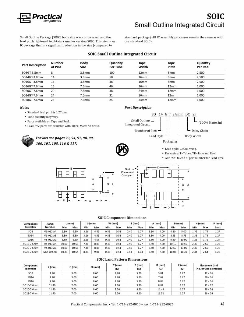
45Practical Components, Inc. • Tel: 1-714-252-0010 • Fax: 1-714-252-0026
B
A S L
HWP
D
G Z
Y
C
E X
GridPlacementCourtyard
Small Outline Package (SOIC) body size was compressed and the lead pitch tightened to obtain a smaller version SOIC. This yields an IC package that is a significant reduction in the size (compared to
standard package). All IC assembly processes remain the same as with our standard SOICs.
Notes � Standard lead pitch is 1.27mm. � Tube quantity may vary. � Parts available on Tape and Reel. � Lead-free parts are available with 100% Matte Sn finish.
For kits see pages 93, 94, 97, 98, 99,100, 101, 105, 116 & 117.
SOIC Component DimensionsComponent
IdentifierJEDEC
NumberL (mm) S (mm) W (mm) T (mm) A (mm) B (mm) H (mm) P (mm)
Min Max Min Max Min Max Min Max Min Max Min Max Min Max BasicSO8 MS-012 AA 5.80 6.30 3.26 4.55 0.33 0.51 0.40 1.27 3.80 4.00 4.80 5.00 1.35 1.75 1.27
SO14 MS-012 AB 5.80 6.30 3.26 4.55 0.33 0.51 0.40 1.27 3.80 4.00 8.55 8.75 1.35 1.75 1.27SO16 MS-012 AC 5.80 6.30 3.26 4.55 0.33 0.51 0.40 1.27 3.80 4.00 9.80 10.00 1.35 1.75 1.27
SO16-7.6mm MS-013 AA 10.00 10.65 7.46 8.85 0.33 0.51 0.40 1.27 7.40 7.60 10.10 10.50 2.35 2.65 1.27SO20-7.6mm MS-013 AC 10.00 10.65 7.46 8.85 0.33 0.51 0.40 1.27 7.40 7.60 12.60 13.00 2.35 2.65 1.27SO28-7.6mm MO-119 AB 10.29 10.64 8.21 9.01 0.36 0.51 0.53 1.04 7.40 7.60 18.08 18.39 2.34 2.64 1.27
SOIC Land Pattern DimensionsComponent
Identifier Z (mm) G (mm) X (mm)Y (mm) C (mm) D (mm) E (mm) Placement Grid
(No. of Grid Elements)Ref Ref Ref RefSO8 7.40 3.00 0.60 2.20 5.20 3.81 1.27 12 x 16
SO14 7.40 3.00 0.60 2.20 5.20 7.62 1.27 20 x 16SO16 7.40 3.00 0.60 2.20 5.20 8.89 1.27 22 x 16
SO16-7.6mm 11.40 7.00 0.60 2.20 9.20 8.89 1.27 22 x 22SO20-7.6mm 11.40 7.00 0.60 2.20 9.20 11.43 1.27 28 x 24SO28-7.6mm 11.40 7.00 0.60 2.20 9.20 16.51 1.27 38 x 24
� Lead Style: G=Gull Wing. � Packaging: T=Tubes, TR=Tape and Reel. � Add “Sn” to end of part number for Lead-Free.
SOICSmall Outline Integrated Circuit
SOIC Small Outline Integrated Circuit
Part Description Number of Pins
Body Size
Quantity Per Tube
Tape Width
Tape Pitch
Quantity Per Reel
SO8GT-3.8mm 8 3.8mm 100 12mm 8mm 2,500SO14GT-3.8mm 14 3.8mm 50 16mm 8mm 2,500SO16GT-3.8mm 16 3.8mm 48 16mm 8mm 2,500SO16GT-7.6mm 16 7.6mm 46 16mm 12mm 1,000SO20GT-7.6mm 20 7.6mm 38 24mm 12mm 1,000SO24GT-7.6mm 24 7.6mm 31 16mm 12mm 1,000SO28GT-7.6mm 28 7.6mm 25 24mm 12mm 1,000
Part Description
SO 14 G T 3.8mm DC Sn
Small Outline Integrated Circuit (100% Matte Sn)
Number of Pins Daisy ChainLead Style Body Width
Packaging

46 Practical Components, Inc. • www.TrustPCI.com • [email protected]
Thin Small Outline Packages (TSOP) are thin body size components; thickness is 1.0mm. TSOP packages have four sides and are rectangular. Type I TSOPs have the leads protruding from the width portion of the package. Lead counts range from 28 to 48. Package body size ranges from 8x11.8mm to 12x20mm.
TYPE I TYPE II
Notes � Standard packaging is in JEDEC trays. � Body dimensions are measured by body length and width. � Type I means that pins extend from the narrow end (the width) of the
body. � Parts available on Tape and Reel. � Type II means that pins extend from the wide end (the length) of the
body. Type II TSOP are becoming obsolete. Practical has some stock. Please call for availability.
� Add “TR” to end of part number for Tape and Reel.
TSOP Thin Small Outline Package – Type IIType II TSOP are becoming obsolete. Practical has some stock. Please call for availability.
TSOPThin Small Outline Package
TSOP Thin Small Outline Package – Type I
Part Description Number of Pins
Body Size
Lead Pitch
Quantity Per Tray
Tape Width
Tape Pitch
Quantity Per Reel
A-T1-TSOP28-8.1x11.8mm-.55mm 28 8.1x11.8mm .55mm 234 24mm 12mm 1,000A-T1-TSOP32-8x11.8mm-.5mm 32 8x11.8mm .5mm 234 24mm 12mm 1,000A-T1-TSOP32-8x18.4mm-.5mm 32 8x18.4mm .5mm 156 32mm 12/16mm 1,000A-T1-TSOP48-12x18.4mm-.5mm 48 12x18.4mm .5mm 96 32mm 16mm 1,000
Part Description System
Amkor A T1 TSOP 28 8.1x11.8mm .5mm DC Sn
Type 1 (100% Matte Sn)
Thin Small Outline Package Daisy Chain
Number of Pins Body Size Pitch

47Practical Components, Inc. • Tel: 1-714-252-0010 • Fax: 1-714-252-0026
The Thin Shrink Small Outline Package (TSSOP) offers smaller body sizes, smaller lead pitches and package thickness (0.9mm thick) than standard SOIC packages. Body widths are 3.0mm, 4.4mm and 6.1mm. Lead counts range from 8 to 80. This package conforms to JEDEC package outlines.
Notes � Tube quantity may vary. � Parts available on Tape and Reel. � 0.9mm body thickness for 4.4 and 6.1mm body widths. � 0.85mm body thickness for 3.0mm body width. � JEDEC package outline is standard. � High conductivity copper leadframes. � Very low-stress mold compound. � Lead-free available with 100% Matte Sn alloy.
TSSOP Package
� Packaging: “T” = Tubes, “TR” = Tape and Reel. � Add “Sn” to end of part number for Lead-Free.
Die Attach Adhesive
MoldCompoundAu Wire
Cu Leadframe
Die
Die Attach Pad
For kit see page 97.
TSSOPThin Shrink Small Outline Package
TSSOP Thin Shrink Small Outline Package
Part Description Number of Pins
Body Size
Lead Pitch
Quantity Per Tube
Tape Width
Tape Pitch
Quantity Per Reel
A-TSSOP8T-3.0mm 8 3.0mm .65mm 98 12mm 8mm 2,500A-TSSOP8T-4.4mm 8 4.4mm .65mm 100 12/16mm 8mm 1,000/2,500A-TSSOP10T-3.0mm 10 3.0mm .5mm 98 12mm 8mm 2,500A-TSSOP14T-4.4mm 14 4.4mm .65mm 96 12/16mm 8mm 1,000/2,500A-TSSOP16T-4.4mm 16 4.4mm .65mm 96 12/16mm 8mm 1,000/2,500A-TSSOP20T-4.4mm 20 4.4mm .65mm 74 16mm 8/12mm 1,000/2,500A-TSSOP24T-4.4mm 24 4.4mm .65mm 62 16mm 8/12mm 1,000/2,500A-TSSOP28T-4.4mm 28 4.4mm .65mm 50 16mm 8/12mm 1,000A-TSSOP44T-4.4mm 44 4.4mm .5mm 42 24mm 12mm 1,000A-TSSOP48T-6.1mm 48 6.1mm .5mm 39 24mm 12mm 1,000A-TSSOP56T-4.4mm 56 4.4mm .4mm 42 24mm 12mm 1,000A-TSSOP56T-6.1mm 56 6.1mm .5mm 35 24mm 12mm 1,000A-TSSOP80T-6.1mm 80 6.1mm .4mm 28 N/A N/A N/A
Part Description System
Amkor A TSSOP 8 T 3.0mm DC Sn
Thin Small Outline Package
(100% Matte Sn)
Number of Pins Daisy Chain
Packaging Body Width

48 Practical Components, Inc. • www.TrustPCI.com • [email protected]
The Shrink Small Outline Package (SSOP) body size is compressed and the lead pitch is tightened to obtain a small version of the standard SOIC packages. Lead counts range from 8 to 64. Body sizes are 209 and 300 mils. The SSOP package is JEDEC and EIAJ compliant. The package leads are solder plated.
Die Attach AdhesiveDie Attach Pad
MoldCompoundAu Wire
Cu Leadframe
Die
Au Wire
DiMoldCompoundCu Leadframe
Exposed Pad
Die AttachAdhesive
Exposed Pad
Die
Note: Drawings not to scale.
Notes � Tube quantity may vary. � Parts available on Tape and Reel. � 209 and 300 mil body widths. � JEDEC and EIAJ package outline standard compliance. � High-conductivity copper leadframes. � Moisture sensitivity is JEDEC level 3. � Lead-free available with 100% Matte Sn alloy.
� Packaging: “T” = Tubes, “TR” = Tape and Reel. � Add “Sn” to end of part number for Lead-Free.
For kits see pages 105, 108 & 117.
SSOPShrink Small Outline Package
SSOP Shrink Small Outline Package
Part Description Number of Pins
Body Size
Lead Pitch
Quantity Per Tube
Tape Width
Tape Pitch
Quantity Per Reel
A-SSOP14T-5.3mm 14 5.3mm .65mm 100 16mm 12mm 1,000A-SSOP16T-5.3mm 16 5.3mm .65mm 80 16mm 12mm 1,000A-SSOP20T-5.3mm 20 5.3mm .65mm 62 16mm 12mm 1,000A-SSOP24T-5.3mm 24 5.3mm .65mm 66 16mm 12mm 1,000A-SSOP28T-5.3mm 28 5.3mm .65mm 47 16/24mm 12mm 1,000A-SSOP36T-7.6mm 36 7.6mm .8mm 31 24mm 12mm 1,000A-SSOP48T-7.6mm 48 7.6mm .635mm 30 32mm 12mm/16mm 1,000A-SSOP56T-7.6mm 56 7.6mm .635mm 26 32mm 12mm/16mm 500
Part Description System
Amkor A SSOP 20 T 5.3mm DC Sn
Shrink Small Outline Package
(100% Matte Sn)
Number of Pins Daisy Chain
Packaging Body Width
Practical Components is the exclusive distributor of Amkor Technology Mechanical Components.
Looking for Lead-Free?
This symbol indicates that lead-free parts are available!

49Practical Components, Inc. • Tel: 1-714-252-0010 • Fax: 1-714-252-0026
Looking for Lead-Free?
This symbol indicates that lead-free parts are available!
The Practical Components B-52 CRET (Cleanliness & Residue Evaluation Test) Kit
The electronics industry's primary test vehicle (TV) for evaluating flux chemistries and surface insulation resistance (SIR)
� The main SIR test board
� The Ion Chromatography (IC) test coupon
� The solder mask adhesion coupons
� The SIR mini-coupons
Test Your Cleanliness to IPC-9201, IPC-9202 & IPC-9203 Standards
The B-52 Rev. B board is the newest revision of the existing B-52 CRET board. The B-52 Rev. B board continues to provide a platform for the electronic assembly industry to evaluate the cleanliness of the assembly process.
Practical Components provides both test PCB boards and components to help verify your cleaning process to meet IPC standards. Practical also has a number of test PCB boards which can be assembled with our dummy components to be
used with conformal coating or adhesive applications for evaluation.
Practical can also customize any board or provide a clean sheet design.
For More Information Call Now! 888-388-7808
For kits see pages 84, 85, 86,87, 88, 89, 90, & 91.

50 Practical Components, Inc. • www.TrustPCI.com • [email protected]
Advanced Wafer Packages
TEG Wafers and Test ElementsPractical Components is the exclusive distributor of Walts Co., LTD In the U.S.A. Walts provides next-generation assembly technology for semiconductors with leading-edge technologies. As the de facto standard, Walts products are used in research and development sites worldwide.
Their well experienced designers can also custom-make TEG (Test Element Groups) to better suit your needs. A wide variety of film sputtering and deposition, back grinding, dicing, bump forming, assembling and analysis are available.
Cu Pillar Bump
Electroless Plating Bump
Solder Bump
TSV
Wafer Specifications
Wafer Size φ 4inch ~ φ 12inchWafer Thickness min. 10μm
Bump MaterialsSolder Bump (High Lead, Lead Free, Eutectic) Gold Bump (Plate, Stud) Copper Bump (Plate, Pillar, Stud)
Minimum PitchFull Area: min. 40μmPeripheral: min. 20μm
min. 20μm (Gold Plate)Deposition SiN, PBO, Polyimide, Back Side Metallization etc.
Advanced Wafer Technology

51Practical Components, Inc. • Tel: 1-714-252-0010 • Fax: 1-714-252-0026
Material
ProductPage Au Solder
Cu NiElectroless
Ni/Au— +SnAg +Ni+SnAg +NiAu — +SnAg
Plate Stud Plate Mount Plate Plate Plate Plate Plate Plate Plate
MB50 52 • • • — • • • • • • —
MB60 52 • • • — • • • • • • —
MB80 53 • • • — • • • • • • —
MB130 54 • • • — • • • • • • •CC40 55 • — • — • • • • • • —
IP40 56 — — — — • • • • • • •IP40A 56 — — — — • • — — — — •CC80 57 • • • — • • • • • • —
IP80 58 — — — — • • • • • • •CC80TSV 59 — — — — — • • — — — •/ ■
CC80Mark II 59 • • • — • • • • • • —
FC150 60 — — • • • • • • • • •FC150LC 61 — — — — • • — — — — —
FC150SC 61 — — • • • • • • • • •FC200 62 — — • • • • • • • • •
FC200SC 63 — — • • • • • • • • •FBW 64 — — — — • • • — — — —
WLP 65 — — — • — — — — — — —
Free Cut Size 65 — — — • — — — — — — —
ME 66 — — — — • — — — — — —
STAC 67 • • • — • • • • • • —
STAC150FA 67 — — — — • • • • • • —
STAC300FA 67 — — — — • • • • • • —
PWB 68 — — — — — — — — — — —
HPW 68 • • • — • • • • • • —
HPW150FA 69 — — — — • • • • • • —
HPW300FA 69 — — — — • • • • • • —
HPWTSV 69 — — — — — • — — — — ■
LCD30 70 • — • — • • • • • • •• Top Side ■ Bottom Side
Advanced Wafer Package Line Up

52 Practical Components, Inc. • www.TrustPCI.com • [email protected]
MB50-0101JY
Chip Structure � Base Layer: P-TEOS* � Metal layer: TiN / Al-0.5%Cu � Passivation Layer: HDP* / P-SiN
(option) Polyimide
*TEOS: Tetraethoxysilane*HDP: High Density Plasma
MB60-0101JY
Specifications
Wafer Size 8 inchWafer Thickness 725±25μmChip Size 7.3mm ■Pad pitch 60μmFunction Daisy ChainPad config Peripheral
Electrode
Au-stud Bump Wire Bonding Au Plating Cu pillar
Pad Size 56μm ■Passivation opening 50μm ■Scribe width 120μmNumber of Pad 448 pads/chipNumber of Chip 478 chips/wafer
■ Bottom Side
Chip Structure � Base Layer: P-TEOS* � Metal layer: TiN / Al-0.5%Cu � Passivation Layer: HDP* / P-SiN
(option) Polyimide
*TEOS: Tetraethoxysilane*HDP: High Density Plasma
Specifications TYPE-A TYPE-B TYPE-C(Glass)
Wafer Size 8 inch 8 inch 8 inch(Glass wafer)Wafer Thickness 725±25μm 725±25μm 700±70μmChip Size 7.3mm ■ 7.3mm ■ 7.3mm ■Pad Pitch 50μm 50μm 50μFunction Daisy Chain Daisy Chain ―Pad config Peripheral Peripheral Peripheral
Electrode Au-Stud Bump Wire Bonding
Cu-Pillar Au-Plated Solder Plated Ni on Cu-Pillar
Cu-Pillar
Pad Size 48μm ■ 48μm ■ ―
Bump Size ―Cu, Au:30μm ■ Cu:30μm ■
Cu:φ25μm ● Cu:φ25μm ●Bump Height ― any anyPassivation Opening 40μm ■ φ15μm ● ―Scribe Width 120μm 120μm ―Number of Pad 544 pads/chip 544 pads/chip ―Number of Chip 478 chips/wafer 478 chips/wafer 478 chips/wafer
● Top Side ■ Bottom Side
For kit see page 71.

53Practical Components, Inc. • Tel: 1-714-252-0010 • Fax: 1-714-252-0026
MB80-STG0101JY
Specifications TYPE-A TYPE-B
Wafer Size 8 inch 8 inchWafer Thickness 725±25μm 725±25μmChip Size 7.3mm ■ 7.3mm ■Pad pitch 80μm staggered 80μm staggeredFunction Daisy Chain Daisy ChainPad config Peripheral PeripheralElectrode Wire Bonding Cu pillarPad Size 76μm ■ 76μm ■Bump Size - 38μm ■Passivation opening 70μm ■ 70μm ■Scribe width 120μm 120μm
Number of Pad648 pads/chip 82pads×4(Outer line) 80pads×4(Inner line)
648 pads/chip 82pads×4(Outer line) 80pads×4(Inner line)
Number of Chip 478 chips/wafer 478 chips/wafer■ Bottom Side
Chip Structure � Base Layer: P-TEOS* � Metal layer: Ti / TiN / Al-0.5%Cu / TiN � Passivation Layer: HDP* / P-SiN
(option) Polyimide
*TEOS: Tetraethoxysilane*HDP: High Density Plasm
AS8R
Specifications
Wafer Size 8 inchWafer Thickness 725±25μmChip Size 3.5mm ■Pad pitch 120μmFunction Daisy ChainPad config Peripheral
Electrode Wire Bonding Stud Bump
Pad Size 115μm×125μmPassivation opening 95μm×100μmScribe width 120μm
Number of Pad 96 pads (Outer line) 88 pads (Inner line)
Number of Chip 2266 chips/wafer■ Bottom Side
(Outer Line) (Inner Line)
Chip Structure � Base Layer: P-TEOS* � Metal layer: Ti / TiN / Al-0.5%Cu / TiN � Passivation Layer: P-TEOS* / P-SiN
*TEOS: Tetraethoxysilane

54 Practical Components, Inc. • www.TrustPCI.com • [email protected]
MB130-STG0101JY & MB130A-STG0101JY
MB6020-0102JY
Specifications MB130 (Type-A) MB130 (TYPE-B) MB130A
Wafer Size 6 inch 6 inch 8 inchWafer Thickness 550±25μm 550±25μm 725±25μmChip Size 2.13mm ■ 2.13mm ■ 2.13mm ■Pad pitch 130μm 130μm 130μmMetal Thickness 0.8μm 0.8μm 1μm or 2μm or 3μmFunction Daisy Chain Daisy Chain Daisy ChainPad config Peripheral Peripheral Peripheral
Electrode Wire Bonding Au Stud Bump Cu Pillar Bump Wire Bonding
Au Stud Bump
Pad Size 100μm ■ 100μm ■ 100μm ■Passivation opening 80μm ■ 80μm ■ 80μm ■Polyimide opening 80μm ■ 80μm ■ 90μm ■Bump Size - 70μm ■ -Scribe width 50μm 50μm 60μm
Number of Pad108 pads/chip 15pads×4 (Outer line) 12pads×4 (Inner line)
108 pads/chip 15pads×4 (Outer line) 12pads×4 (Inner line
108 pads/chip 15pads×4 (Outer line) 12pads×4 (Inner line)
Number of Chip 3300 chips/wafer 3300 chips/wafer 6060 chips/wafer■ Bottom Side
Chip Structure � MB130
� Base Layer: P-TEOS* � Metal layer: TiW/ Al-1.0%Si-0.5%Cu � Passivation Layer: P-TEOS* / P-SiN (option) Polyimide
� MB130A � Base Layer: P-TEOS* � Metal layer: Ti / TiN / Al-1.0%Si-0.5%Cu
� Passivation Layer: P-TEOS* / P-SiN (option) Polyimide
*TEOS: Tetraethoxysilane
Specifications
Wafer Size 8 inchWafer Thickness 725±25umChip Size 3.0mm ■Pad Pitch 60/55/50/45/40/35/30/25/20Metal Thickness 0.6μm or 0.8μmFunction Daisy ChainPad Config PeripheralElectrode Wire Bonding
Pad Size(57×110μm) (52×110μm) (47×110μm) (42×110μm) (37×110μm) (32×110μm) (27×110μm) (22×110μm) (17×110μm)
Passivation Opening(53×100μm) (48×100μm) (43×100μm) (38×100μm) (33×100μm) (28×100μm) (23×100μm) (18×100μm) (13×100μm)
Scribe Width 100μm
Number of Pad(40×4) (40×4) (38×4) (38×4) (36×4) (34×4) (30×4) (26×4) (18×4)
Number of Chip 3016 chips/wafer■ Bottom Side
Chip Structure � Base Layer: P-TEOS* � Metal layer: TiN / Al-0.5%Cu � Passivation Layer: HDP* / P-SiN
*TEOS: Tetraethoxysilane*HDP: High Density Plasma

55Practical Components, Inc. • Tel: 1-714-252-0010 • Fax: 1-714-252-0026
CC40-0101JY
Chip Structure � Base Layer: P-TEOS* � Metal layer: TiN / Al-0.5%Cu � Passivation Layer: HDP* / P-SiN
*TEOS: Tetraethoxysilane*HDP: High Density Plasma
Specifications
Wafer Size 8 inchWafer Thickness 725±25umChip Size 7.3mm ■
Pad Pitch 40μm pitch Full area + Staggered (Model I) 40μm pitch Staggered (Model II)
Function Daisy Chain
Pad Config Full Area (Model I) Peripheral (Model II)
Electrode Cu pillarPad Size 32μm ■Passivation Opening 7μm ●Scribe Width 120μmNumber of Chip 478 chips/wafer
● Top Side ■ Bottom Side
Bump Layout Bump Size Number of Bumps
Model I φ22um 29576Model II φ22um 1352

56 Practical Components, Inc. • www.TrustPCI.com • [email protected]
IP40-0101JY & IP40A-0101JY
Specifications IP40(Model I) IP40A(Model I) IP40(Model II)
Wafer Size 8 inch 12 inch 8 inchWafer Thickness 725±25um 775±25um 725±25umChip Size 10.0mm 10.0mm 10.0mm
Pad Pitch � 40μm pitch Full Area + Staggered � 250μm pitch Peripheral
� 40μm pitch Staggered � 250μm pitch Peripheral
Function Daisy Chain / Bump Short Check / Vernier Breakdown Voltage Check between the Bumps
Pad Config Full Area PeripheralPad Size � 32 μm ■ � 110 μm ■Passivation Opening � 20 μm ● � 100 μm ■Scribe Width 100μmNumber of Pad �29576 pads �124 pads �1352 pads �124 padsNumber of Chip 228 chips/wafer 616 chips/wafer 228 chips/waferSurface Spec of Round Electroless Ni/Au plating
● Top Side ■ Bottom Side
Chip Structure � IP40
� Base Layer: P-TEOS* � Metal layer: TiN / Al-0.5%Cu � Passivation Layer: HDP* / P-SiN
� IP40A � Base Layer: P-TEOS* � Metal layer: TiN / Al-0.5%Cu � Passivation Layer: P-SiO / P-SiN
*TEOS: Tetraethoxysilane*HDP: High Density Plasma

57Practical Components, Inc. • Tel: 1-714-252-0010 • Fax: 1-714-252-0026
Concept of CC80 Series
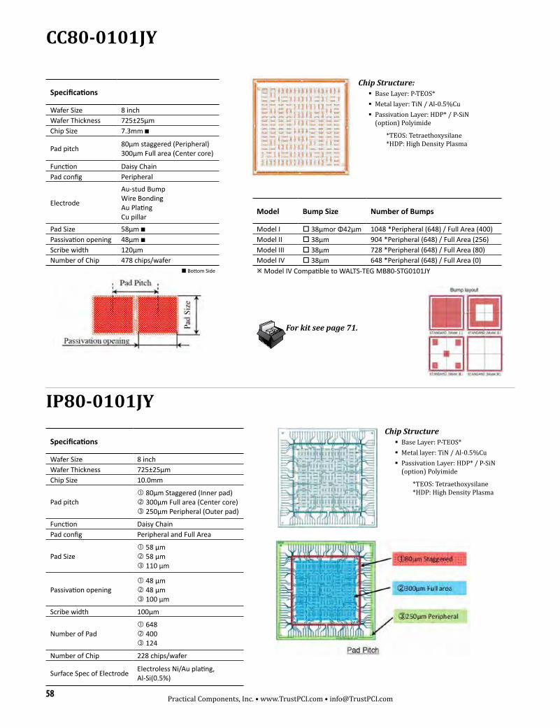
58 Practical Components, Inc. • www.TrustPCI.com • [email protected]
CC80-0101JY
Chip Structure: � Base Layer: P-TEOS* � Metal layer: TiN / Al-0.5%Cu � Passivation Layer: HDP* / P-SiN
(option) Polyimide
*TEOS: Tetraethoxysilane*HDP: High Density Plasma
Specifications
Wafer Size 8 inchWafer Thickness 725±25μmChip Size 7.3mm ■
Pad pitch 80μm staggered (Peripheral) 300μm Full area (Center core)
Function Daisy ChainPad config Peripheral
Electrode
Au-stud Bump Wire Bonding Au Plating Cu pillar
Pad Size 58μm ■Passivation opening 48μm ■Scribe width 120μmNumber of Chip 478 chips/wafer
■ Bottom Side
Model Bump Size Number of Bumps
Model I o 38μmor Φ42μm 1048 *Peripheral (648) / Full Area (400)Model II o 38μm 904 *Peripheral (648) / Full Area (256)Model III o 38μm 728 *Peripheral (648) / Full Area (80)Model IV o 38μm 648 *Peripheral (648) / Full Area (0)ø Model IV Compatible to WALTS-TEG MB80-STG0101JY
IP80-0101JY
Specifications
Wafer Size 8 inchWafer Thickness 725±25μmChip Size 10.0mm
Pad pitch� 80μm Staggered (Inner pad) � 300μm Full area (Center core) � 250μm Peripheral (Outer pad)
Function Daisy ChainPad config Peripheral and Full Area
Pad Size� 58 μm � 58 μm � 110 μm
Passivation opening� 48 μm � 48 μm � 100 μm
Scribe width 100μm
Number of Pad� 648 � 400 � 124
Number of Chip 228 chips/wafer
Surface Spec of Electrode Electroless Ni/Au plating, Al-Si(0.5%)
Chip Structure � Base Layer: P-TEOS* � Metal layer: TiN / Al-0.5%Cu � Passivation Layer: HDP* / P-SiN
(option) Polyimide
*TEOS: Tetraethoxysilane*HDP: High Density Plasma
For kit see page 71.

59Practical Components, Inc. • Tel: 1-714-252-0010 • Fax: 1-714-252-0026
Specifications CC80TSV-1 CC80TSV-2
Wafer Size 8 inch 8 inchWafer Thickness 100μm 100μmChip Size 7.3mm ■ 7.3mm ■
Pad pitch 80μm staggered (Peripheral) 300μm Full area (Center core)
80μm staggered (Peripheral) 300μm Full area (Center core)
TOP SideElectrode Electroless Ni/Au plating Electrode Cu + SnAgBump Size Φ48μm (Option: φ42um) Bump Size 38μm ■ (Option: φ42um)Bump Height 8 ~ 12um Bump Height Cu20μm + SnAg15μm
BOTTOM SideElectrode Electroless Ni/Au plating Electrode Electroless Ni/Au platingBump Size Φ48μm (Option: φ42um) Bump Size Φ48μm (Option: φ42um)Bump Height 8 ~ 12um Bump Height 8 ~ 12um
Scribe width 120μm 120μm■ Bottom Side
CC80 MarkII-0101JY (STD)
Specifications STD
Wafer Size 8 inch (Notch)Wafer Thickness 725±25μmChip Size 12.0mm ■Function Daisy Chain & Migration
Pad PitchPeripheral 80μm Three Rows Staggered
Center core 200μm Full AreaElectrode Cu PillarPad Size 54μm ■Bump Size φ31μmPassivation opening 48μm ■Scribe width 120μm
Number of Bump/PadPeripheral 1660 bumps / 1660 pads
Center core 2916 bumps / 2916 padsNumber of Chip 177 chips/wafer
■ Bottom Side
Chip Structure � Base Layer: P-TEOS* � Metal layer: TiN / Al-0.5%Cu � Passivation Layer: HDP* / P-SiN
*TEOS: Tetraethoxysilane*HDP: High Density Plasma
CC80TSV-0101JY
60 Practical Components, Inc. • www.TrustPCI.com • [email protected]
FC150JY
Chip Structure � Base Layer: P-TEOS* � Metal layer: TiN / Al-0.5%Cu � Passivation Layer: HDP* / P-SiN
(option) Polyimide
*TEOS: Tetraethoxysilane*HDP: High Density Plasma
Specifications Si Glass
TYPE A B A BWafer Thickness 725±25μm 725±25μm 700±70μm 700±70μmWafer Size 8 inch 8 inch 8 inch 8 inchChip Size 10.0mm ■ 10.0mm ■ 10.0mm ■ 10.0mm ■Bump pitch 150μm 150μm 150μm 150μmFunction Daisy Chain Daisy Chain ― ―Pad config Area Area Area AreaElectrode Ball Mounted Solder Bump Cu Pillar Ball Mounted Solder Bump Cu PillarPad Size 100μm ■ 100μm ■ ― ―Passivation opening φ40μm ● φ40μm ● ― ―Polyimide opening φ60μm ● φ60μm ● ― ―UBM Size φ80μm ● φ75μm ● φ80μm ● φ75μm ●Bump Size φ85μm ● φ75μm ● φ85μm ● φ75μm ●Scribe width 100μm 100μm ― ―Number of Pad 3721pads/chip(61×61) 3721pads/chip(61×61) ― ―Number of Chip 208 chips/wafer 208 chips/wafer 208 chips/wafer 208 chips/wafer
● Top Side ■ Bottom Side
For kit see page 71.
61Practical Components, Inc. • Tel: 1-714-252-0010 • Fax: 1-714-252-0026
FC150LC-0101JY
Chip Structure � Base Layer: P-SiO � Metal layer: TiN / Al-Si � Passivation Layer: P-SiO / P-SiN
(option) Polyimide
Specifications
Wafer size φ300mmWafer Thickness 775±25umChip size 25mm * 25 mm (Scribe center to center)Pad (bump)pitch 150μmFunction Daisy ChainElectrode Cu pillar (Cu30μm+SnAg15μm)Bump size φ75μmPassivation opening 40μm (octagon)Polyimide opening φ40μmScribe line width 100μmNumber of pad 25,921 pads (161×161 Matrix)
FC150SCJY
Chip Structure � Base Layer: P-TEOS* � Metal layer: TiN / Al-0.5%Cu � Passivation Layer: HDP* / P-SiN
(option) Polyimide
*TEOS: Tetraethoxysilane*HDP: High Density Plasma
TYPE A B
Wafer Thickness 725±25μm 725±25μmWafer Size 8 inch 8 inchChip Size 5.02mm ■ 5.02mm ■Bump pitch 150μm 150μmFunction Daisy Chain Daisy ChainPad config Area AreaElectrode Ball Mounted Solder Bump Cu PillarPad Size 100μm ■ 100μm ■Passivation opening φ40μm ● φ40μm ●Polyimide opening φ60μm ● φ60μm ●UBM Size φ80μm ● φ75μm ●Bump Size φ85μm ● φ75μm ●Bump height any anyScribe width 100μm 100μmNumber of Pad 784 pads/chip (28×28)784 pads/chip (28×28)Number of Chip 832 chips/wafer 832 chips/wafer
● Top Side ■ Bottom Side

62 Practical Components, Inc. • www.TrustPCI.com • [email protected]
FC200JY
Specifications Si Glass
TYPE A B A BWafer Size 8 inch 8 inch 8 inch 8 inchWafer Thickness 725±25μm 725±25μm 700±70μm 700±70μmChip Size 10.0mm ■ 10.0mm ■ 10.0mm ■ 10.0mm ■Bump pitch 200μm 200μm 200μm 200μmFunction Daisy Chain Daisy Chain ― ―Pad config Area Area Area AreaElectrode Ball Mounted Solder Bump Cu Pillar Ball Mounted Solder Bump Cu PillarPad Size 100μm ■ 100μm ■ ― ―Passivation opening φ60μm ● φ60μm ● ― ―Polyimide opening φ80μm ● φ80μm ● ― ―UBM Size φ100μm ● φ90μm ● φ100μm ● φ90μm ●Bump Size φ100μm ● φ90μm ● φ100μm ● φ90μm ●Scribe width 100μm 100μm ― ―Number of Pad 2116 pads/chip (46×46) 2116 pads/chip (46×46) ― ―Number of Chip 228 chips/wafer 228 chips/wafer 228 chips/wafer 228 chips/wafer
● Top Side ■ Bottom Side
Chip Structure � Base Layer: P-TEOS* � Metal layer: TiN / Al-0.5%Cu � Passivation Layer: HDP* / P-SiN
(option) NSG* / Polyimide
*TEOS: Tetraethoxysilane*HDP: High Density Plasma*NSG: Non-doped Silicate Glass
For kit see page 71.

63Practical Components, Inc. • Tel: 1-714-252-0010 • Fax: 1-714-252-0026
FC200SCJY
Chip Structure � Base Layer: P-TEOS* � Metal layer: TiN / Al-0.5%Cu � Passivation Layer: HDP* / P-SiN
(option) Polyimide
*TEOS: Tetraethoxysilane*HDP: High Density Plasma
Specifications Si
TYPE A BWafer Size 8 inch 8 inchWafer Thickness 725±25μm 725±25μmChip Size 5.02mm ■ 5.02mm ■Bump pitch 200μm 200μmFunction Daisy Chain Daisy ChainPad config Area AreaElectrode Ball Mounted Solder Bump Cu PillarPad Size 100μm ■ 100μm ■Passivation opening φ60μm ● φ60μm ●Polyimide opening φ80μm ● φ80μm ●UBM Size φ100μm ● φ90μm ●Bump Size φ100μm ● φ90μm ●Scribe width 100μm 100μmNumber of Pad 484 pads/chip (22×22) 484 pads/chip (22×22)Number of Chip 832 chips/wafer 832 chips/wafer
● Top Side ■ Bottom Side

64 Practical Components, Inc. • www.TrustPCI.com • [email protected]
FBW
Specifications FBW200-0001JY FBW150-0001JY FBW130-0001JY FBW100-0001JY FBW80-0001JY
Wafer Size 8 inch 8 inch 8 inch 8 inch 8 inchWafer Thickness 725±25μm 725±25μm 725±25μm 725±25μm 725±25μmBump Pitch 200μm 150μm 130μm 100μm 80μmFunction ― ― ― ― ―Electrode Cu Pillar Cu Pillar Cu Pillar Cu Pillar Cu PillarBump Size φ90μm φ75μm φ65μm φ50μm φ40μmBump Height Max.60μm Max.60μm Max.60μm Max.60μm Max.50μm

65Practical Components, Inc. • Tel: 1-714-252-0010 • Fax: 1-714-252-0026
WLP TEG 0.4mm pitch BGA 0.3mm pitch BGA
Wafer Size 8 inch 8 inchWafer Thickness 400±20μm 400±20μmChip Size 6.0mm ■ 6.0mm ■BGA pitch 400μm 300μmFunction Daisy Chain Daisy ChainElectrode Ball Mounted Solder Bump Ball Mounted Solder BumpPad Size (φ227μm) (φ177μm)Line width 25μm 20μmNumber of Pin 144 pins/chip 264 pins/chipNumber of Chip 712 chips/wafer 712 chips/wafer
■ Bottom Side
WLP TEG (Free Size Cut TEG: TEG0306, TEG0408, TEG0510)
Free Size Cut TEG TEG0306 TEG0408 TEG0510
Wafer Size 8 inch 8 inch 8 inchWafer Thickness 400μm(or more) 400μm(or more) 400μm(or more)
Cut Size (Scribe Line Included) Min 600μm×600μm 800μm×800μm 1000μm×1000μm
Pad Pitch 300μm 400μm 500μmFunction Daisy Chain Daisy Chain Daisy ChainElectrode Ball Mounted Solder Bump Ball Mounted Solder Bump Ball Mounted Solder BumpPost Size 175μm 200μm 250μmNumber of Chip 79,257 chips/wafer 44,161 chips/wafer 28,212 chips/wafer
WLP TEG (0.4mm pitch & 0.3mm pitch)

66 Practical Components, Inc. • www.TrustPCI.com • [email protected]
ME0102JY (for Migration Test)
Specifications
Wafer Size 12 inchChip Size 20mm×25mmChip Name Chip_10_15 Chip_20_25 Chip_30_35Metal Height 5.5μmFacing Length 3mmLine/Space 15μm/10μm 15μm/15μm 15μm/20μm 15μm/25μm 15μm/30μm 15μm/35μmPitch 25μm 30μm 35μm 40μm 45μm 50μmNumber of Chip 34 chips/wafer 40 chips/wafer 34 chips/wafer
Chip Structure � Layer: SiO2 / Polyimide / TiCu / Cu (RDL)

67Practical Components, Inc. • Tel: 1-714-252-0010 • Fax: 1-714-252-0026
STAC-0101JY
Specifications
Wafer Size 6inch(OrientationFlat)Wafer Thickness 550±25μmChip Size 3.0mm ■Pad Pitch 300μm
FunctionStress Analysis by Piezoresistance Thermal Analysis by Diode Heat Generation by Resistance
Electrode
Al pad Cu Pillar Bump Solder Bump Au Bump
Pad Size 120μm ■Passivation Opening 70μm (Octagon)Polyimide Opening φ90μmScribe Line Width 80μmNumber of Pad 32pads<Option> Back Side Metallization
■ Bottom Side
STACTEG-150FA-0101JY & STACTEG-300FA-0101JY
Specifications STACTEG-150FA STACTEG-300FA
Base Wafer STAC-0101JY STAC-0101JYElectrode Ni + SnAg Bump Cu Pillar BumpBump Pitch 150μm 300μmBump Size φ110μm φ110μmBump Height Ni5μm+SnAg75μm Cu50um+SnAg10umPassivation Opening 70μm (Octagon) 70μm (Octagon)Polyimide Opening φ90μm φ90μmNumber of Pad 32 pads 32 padsNumber of Bump 32 bumps + 253 Dummy bumps 32 bumps + 64 Dummy bumps<Option> Back Side Metallization Back Side Metallization

68 Practical Components, Inc. • www.TrustPCI.com • [email protected]
HPW-0101JY
Specifications
Wafer Size 8inch (Notch)Wafer Thickness 725±25μmChip Size 3.0mm ■Pad Pitch 300μm
Function Thermal Analysis by Diode Heat Generation by Resistance
Electrode
Al pad Cu Pillar Bump Solder Bump Au Bump
Pad Size 120μm ■Passivation Opening 70μm (Octagon)Polyimide Opening φ90μmScribe Line Width 80μmNumber of Pad 32padsMaximum Output Max. 14.5W/Chip<Option> Back Side Metallization
■ Bottom Side
Chip Structure � Base Layer: SiO2 � Metal layer: Al-1.0%Si � Passivation Layer: P-SiN
Specifications TYPE-A TYPE-B
Wafer Size 6 inch 6 inchWafer Thickness 625±25μm 625±25μmChip Size 6.0mm ■ 6.0mm ■Metal Thickness Al-Si 3μm Al-Si 4.5μmFunction BondabilityCheck BondabilityCheckPad config Plane Plane
Pad Size� 5060μm × 2420μm � 5060μm × 2420μm� 270μm 5300μm � 270μm × 5300μm
Passivation opening� 5040μm × 2400μm � 5040μm × 400μm� 250μm × 5280μm � 250μm × 5280μm
Scribe width 100μm 100μm■ Bottom Side
PWB0101JY

69Practical Components, Inc. • Tel: 1-714-252-0010 • Fax: 1-714-252-0026
HPWTEG-150FA-0101JY & HPWTEG-300FA-0101JY
Specifications HPWTEG-150FA HPWTEG-300FA
Base Wafer HPW-0101JY HPW-0101JYElectrode Ni + SnAg Bump Cu Pillar BumpBump Pitch 150μm 300μmBump Size φ110μm φ110μmBump Height Ni5μm+SnAg75μm Cu50um+SnAg10umPassivation Opening 70μm (Octagon) 70μm (Octagon)Polyimide Opening φ90μm φ90μmNumber of Pad 32 pads 32 padsNumber of Bump 32 bumps + 253 Dummy bumps 32 bumps + 64 Dummy bumps<Option> Back Side Metallization Back Side Metallization
HPWTSV-0101JY
Specifications
Base Wafer HPW-0101JY (SiN)Wafer Thickness 100μm
Top Side
Electrode Cu Pillar BumpNumber of Bump 32 bumps + 64 Dummy bumpsBump Size φ100μmBump Pitch 300μmBump Height Cu50μm+SnAg10μmTop Coat Layer Passivation (P-SiN)
TSV Via Size φ90μm
BottomSide
Electrode Electroless Ni/Au platingNumber of Bump 32 bumpsBump Size φ100μmBump Pitch 300μmBump Height 8μmTop Coat Layer P-TEOS

70 Practical Components, Inc. • www.TrustPCI.com • [email protected]
LCD30-0101JY
Specifications
Wafer Size 6 inchChip Size 15.1mm×1.6mmPad pitch 30μmFunction Daisy ChainPad config PeripheralBump material(process) Gold(plating) , CuPad Size 28μm×120μmPassivation opening 6μm×80μmUBM Size 20μm×100μmBump Size 20μm×100μmScribe width 100μmNumber of Pad 726 pad/chipNumber of Chip 530 chip/wafer
Chip Structure � Base Layer: P-TEOS* � Metal layer: TiW/ Al-1.0%Si-0.5%Cu � Passivation Layer: P-TEOS* / P-SiN
*TEOS: Tetraethoxysilane

71Practical Components, Inc. • Tel: 1-714-252-0010 • Fax: 1-714-252-0026
Advanced Wafer Technology Substrates
Part Description W-Kit-MB50-0102 W-Kit-CC80-0104 W-Kit-FC150P-10 W-Kit-FC200P-10
Specifications 1x1 1x1Structure 1-2-1 Build Up Substrate 1-2-1 Build Up Substrate Rigid Substrate (both) Rigid Substrate (both)Layer Structure
Layer 1 Signal Layer (no via) Layer 2 ~ Layer 4 Mesh
Layer 1,2 Signal Layer (Via) Layer 3, 4 Mesh
Outline 17.0mm x 17.0mm x (0.96mmt)
187.5mm x 64.0mm x (0.36mmt)
30.0mm x 30.0mm x (0.96mmt)
30.0mm x 30.0mm x (0.86mmt)
Core Material Core: E-679FGR Build Layer: ABF-GX13
Core: E-679FGBS Build Layer: ABF-GX92
Core: E-679FGR Build Layer: ABF-GX92 Core: E-679FGR
Solder Resist Material PSR4000 AUS-703 PSR4000 AUS-703 PSR4000 AUS-703 PSR4000 AUS-703
Function Daisy Chain Daisy Chain Daisy Chain Daisy ChainLand Size Φ0.12µm Φ0.14µmLead Min L/S 20µm/30µm 32µm/48µmNumber of Lead 536 lead Peripheral: 648 lead
Full Area: 400 leads 3,721 (61x61) 2,116 (46x46)
Pad Dimensions
Φ0.8µm (SR opening: Φ0.65µm)
Φ0.75µm (SR opening: Φ0.67µm) SR opening: Φ0.80µm SR opening: Φ0.95µm
Number of Pads 32 Pads 72 Pads 24 Pads 24 Pads
Daisy Chain Center Area 16x15 Matrix Corner Area 15x15 four Matrix
Center Area 12x12 Matrix Corner Area 12x11 four Matrix
Surface Spec of Electrode Electroless Ni/Au plating
Cu Cu+OSP Electroless Ni/Au plating
Electroless Ni/Au plating Cu+OSP (Option Solder Coat) Cu
Electroless Ni/Au plating Cu+OSP (Option Solder Coat) Cu
** Call Practical for custom and option kit substrate options
CC80 [Map]
MAP_NCR 2Block in a Sheet (3x5x2Block)
FC150 1x1 FC200 1x1

72 Practical Components, Inc. • www.TrustPCI.com • [email protected]
CTReelsEmpty Carrier Tape Reels
Notes � Taped to EIA 481 standards. � Plastic (PL) carrier tape is standard. Paper (PA) carrier tape is special
order. � Reels come standard with Heat Seal Cover Tape. � PSA available upon request (pressure sensitive adhesive). � 10–100g peel back pressure for 8mm carrier tapes. � 10–130g peel back pressure for 12–56mm carrier tapes. � 10–150g peel back pressure for 72mm carrier tapes. � Additional pocket types available upon request. � Additional widths and pitches may be available, call for details.
Label
Top Cover Tape
Carrier Tape
Sprocket Hole
Cavity
When only the physical characteristics of the tape matter, we offer empty carrier tape reels in a variety of widths and pitches. Empty carrier tape reels are plastic embossed or paper carrier tape with sealed cover tape to simulate running parts without the cost and mess during feeder applications. CTReels are a cost saving alternative compared to actual parts on tape.
Empty Carrier Tape Reels
Part Description Reel Size
Tape Width
Tape Pitch
Standard Pocket
Pockets Per Reel
Tape Type
7”x8mm-CTR-PA 7” 8mm2mm 0402SMR 10,000 Paper4mm 0805SMR 5,000 Paper
7”x8mm-CTR-PL 7” 8mm2mm 0402SMR 10,000 Plastic4mm 0805SMR 5,000 Plastic
7”x12mm-CTR-PL 7” 12mm 8mm 1812SMC 1,000 Paper7”x16mm-CTR-PL 7” 16mm 12mm SO16-7.6mm 500 Plastic13”x8mm-CTR-PA 13” 8mm 4mm 0805SMR 10,000 Paper13”x8mm-CTR-PL 13” 8mm 4mm 0805SMR 10,000 Plastic13”x12mm-CTR-PL 13mm 12mm 8mm SO8-3.8mm 2,500 Plastic
13”x16mm-CTR-PL 13” 16mm8mm SO14-3.8mm 2,500 Plastic12mm SO16-7.6mm 1,000 Plastic
13”x24mm-CTR-PL 13” 24mm
12mm SO20-7.6mm 1,000 Plastic16mm PLCC28 750 Plastic20mm LQFP-12mm 750 Plastic24mm PBGA-13mm 500 Plastic
13”x32mm-CTR-PL 13” 32mm12mm T1-TSOP32 1,000 Plastic16mm T1-TSOP32 1,000 Plastic24mm PLCC44 750 Plastic
13”x44mm-CTR-PL 13” 44mm
16mm T11-TSOP54 500 Plastic20mm TBA 1,000 Plastic24mm LQFP-20mm 750 Plastic32mm PBGA-23mm 250 Plastic36mm TBA 250 Plastic40mm TBA 200 Plastic
13”x56mm-CTR-PL 13” 56mm40mm PBGA-35mm 250 Plastic44mm QFP-32mm 250 Plastic
13”x72mm-CTR-PL 13” 72mm 24mm TBA 300 Plastic
Part Description System
7”x8mm CTR PL
Reel Size & Tape Width Tape Type
Carrier Tape Reel
Tape & Reel
73Practical Components, Inc. • Tel: 1-714-252-0010 • Fax: 1-714-252-0026
Tape and Reel Specifications
Part Description Tape Width
Tape Pitch
Reel Size
Qty Per Reel
01005SMR-PA 8mm 2mm 7" 20,000
0201SMR-PA 8mm 2mm 7" 15,000
0402SMR-PA 8mm 2mm 7" 10,000
0603SMR-PA 8mm 4mm 7" 5,000
0805SMR-PA 8mm 4mm 7" 5,000
1206SMR-PA 8mm 4mm 7" 5,000
1210SMR-PA 8mm 4mm 7" 5,000
0201SMC-PA 8mm 2mm 7" 15,000
0402SMC-PA 8mm 2mm 7" 10,000
0603SMC-PA 8mm 4mm 7" 4,000
0805SMC-PA 8mm 4mm 7" 4,000
1206SMC-PA 8mm 4mm 7" 4,000
0805SMC-PL 8mm 4mm 7" 4,000
1206SMC-PL 8mm 4mm 7" 3,000
1210SMC-PL 8mm 4mm 7" 3,000
1812SMC-PL 12mm 8mm 7" 1,000
1825SMC-PL 12mm 8mm 7" 1,000
3mm-SME-PL 12mm 8mm 13" 2,000
4mm-SME-PL 12mm 8mm 13" 2000
5mm-SME-PL 12mm 12mm 13" 1,000
6.3mm-SME-PL 16mm 12mm 13" 1,000
8mm-SME-PL 16mm 12mm 13" 1,000
10mm-SME-PL 24mm 16mm 13" 500
18mm-SME-PL 44mm 32mm 13" 125
3216SMTA-PL 8mm 4mm 7" 2,000
3528SMTA-PL 8mm 4mm 7" 2,000
6032SMTA-PL 12mm 8mm 7" 500
7343SMTA-PL 12mm 8mm 7" 500
SC90-TR (supermini) 8mm 4mm 7" 3,000
SOT323-TR 8mm 4mm 7" 3,000
SOT353-TR 8mm 4mm 7" 3,000
SOT363-TR 8mm 4mm 7" 3,000
SOT23-TR 8mm 4mm 7" 3,000
SOT25-TR 8mm 4mm 7" 3,000
SOT26-TR 8mm 4mm 7" 3,000
SOT143-TR 8mm 4mm 7" 3,000
SOT89-TR 12mm 8mm 7" 1,000
SOT223-TR 12mm 8mm 7" 1,000
DPAK-TR 16mm 8mm 13" 2,500
D2PAK-TR 24mm 12mm 13" 800/1,000
SO8GTR-3.8mm 12mm 8mm 13" 2,500
SO14GTR-3.8mm 16mm 8mm 13" 2,500
SO16GTR-3.8mm 16mm 8mm 13" 2,500
SO16GTR-7.6mm 16mm 12mm 13" 1,000
SO20GTR-7.6mm 24mm 12mm 13" 1,000
SO28GTR-7.6mm 24mm 12mm 13" 1,000
SO28JTR-7.6mm 24mm 12mm 13" 1,000
SSOP14TR-5.3mm 16mm 12mm 13" 1,000
SSOP16TR-5.3mm 16mm 12mm 13" 1,000
SSOP20TR-5.3mm 16mm 12mm 13" 1,000
SSOP24TR-5.3mm 16mm 12mm 13" 1,000
SSOP28TR-5.3mm 16/24mm 12mm 13" 1,000
SSOP48TR-7.6mm 32mm 12/16mm 13" 1,000
SSOP56TR-7.6mm 32mm 12/16mm 13" 500
Part Description Tape Width
Tape Pitch
Reel Size
Qty Per Reel
TSSOP8TR-3.0mm 12mm 8mm 13" 2,500
TSSOP8TR-4.4mm 12/16mm 8mm 13" 1,000/2,500
TSSOP10TR-3.0mm 12mm 8mm 13" 2,500
TSSOP14TR-4.4mm 12/16mm 8mm 13" 1,000/2,500
TSSOP16TR-4.4mm 12/16mm 8mm 13" 1,000/2,500
TSSOP20TR-4.4mm 16mm 8/12mm 13" 1,000/2,500
TSSOP24TR-4.4mm 16mm 8/12mm 13" 1,000/2,500
TSSOP28TR-4.4mm 16mm 8/12mm 13" 1,000
TSSOP32TR-6.1mm 24mm 12mm 13" 1,000
TSSOP44TR-4.4mm 24mm 12mm 13" 1,000
TSSOP48TR-6.1mm 24mm 12mm 13" 1,000
TSSOP56TR-4.4mm 24mm 12mm 13" 1,000
TSSOP56TR-6.1mm 24mm 12mm 13" 1,000
T1-TSOP28-8.1x11.8mm-.55mm 24mm 12mm 13" 1,000
T1-TSOP32-8x18.4mm-.5mm 32mm 12/16mm 13" 1,000
T1-TSOP48-12x18.4mm-5mm 32mm 16mm 13" 1,000
T11-TSOP32-10.16x20.95mm-1.27mm 32mm 16mm 13" 1,000
T11-TSOP54-10.16x22.22mm-.8mm 44mm 16mm 13" 1,000
PLCC20TR 16mm 12mm 13" 1,000
PLCC28TR 24mm 16mm 13" 750
PLCC32TR 24mm 16mm 13" 750
PLCC44TR 32mm 24mm 13" 450
PLCC68TR 44mm 32mm 13" 230/250
PLCC84TR 44mm 36mm 13" 250
QFP-10mm sq. 24mm 24mm 13" 500
QFP-14mm sq. 32mm 24mm 13" 350
QFP-14x20mm 44mm 32mm 13" 500
QFP-28mm sq. 44mm 40mm 13" 200
QFP-32mm sq. 56mm 44mm 13" 200
LQFP/TQFP- 5mm sq. 16mm 12mm 13" 1,000
LQFP/TQFP- 7mm sq. 16mm 12mm 13" 1,000
LQFP/TQFP- 10mm sq. 24mm 16/24mm 13" 1,000
LQFP/TQFP- 12mm sq. 24mm 20/24mm 13" 1,000
LQFP/TQFP- 14mm sq. 32mm 24mm 13" 750
LQFP/TQFP- 14x20mm 44mm 32mm 13" 500
LQFP/TQFP- 20mm sq. 44mm 24mm 13" 500
LQFP/TQFP- 24mm sq. 44mm 32mm 13" 500
PBGA-13mm sq. 24mm 24mm 13" 500
PBGA-15mm sq. 24mm 24mm 13" 500
PBGA-17mm sq. 24mm 24mm 13" 500
PBGA-23mm sq. 44mm 32mm 13" 250
PBGA-27mm sq. 44mm 32mm 13" 250
PBGA-35mm sq. 56mm 40mm 13" 250
CTBGA/CABGA-5mm sq. 12mm 8mm 13" 1,000
CTBGA/CABGA-6mm sq. 16mm 8mm 13" 1,000
CTBGA/CABGA-7mm sq. 16mm 12mm 13" 1,000
CTBGA/CABGA-8mm sq. 16mm 12mm 13" 1,000
CTBGA/CABGA-9mm sq. 16mm 12mm 13" 1,000
CTBGA/CABGA-10mm sq. 24mm 12mm 13" 1,000
CTBGA/CABGA-11mm sq. 24mm 16mm 13" 1,000
CTBGA/CABGA-12mm sq. 24mm 16mm 13" 1,000
CTBGA/CABGA-14mm sq. 24mm 24mm 13" 500
CTBGA/CABGA-17mm sq. 24mm 24mm 13" 500

74 Practical Components, Inc. • www.TrustPCI.com • [email protected]
Through-Hole Glass DiodesAxial Leaded Through-hole Glass Diode package has been in use for over 50 years in the electronics industry. The body of these parts are glass and the package is hermetically sealed. The “DO” prefix is a JEDEC designation for through-hole diodes. The 34 and 35 references
case size. These type of components are packaged on ammo pack or bulk. In most cases, these parts are sold as training aids to teach new operators how to solder.
Notes � Part is hermetically sealed glass package. � Axial leaded (2 leads). � Parts are packaged Ammo pack (5K per reel) or bulk. � Lead-free available with 100% Sn alloy.
D
b
LG1L
(1)
D
b
LG1L
(1)
DO-34
Unit b Max
D Max G1Max L
Min
mm 0.55 1.6 3.04 25.4
DO-35
Unit b Max
D Max G1Max L
Min
mm 0.56 1.85 4.25 25.4
PDIPPlastic Dual In-Line Package
Plastic Dual In-Line Packages (PDIP) are long-established industry standard through-hole packages.
Notes � High conductivity copper leadframe. � JEDEC standard compliant. � Parts packaged in anti-static 20" tubes. � Pitch is 100 mils. � Lead-free available with 100% Sn Matte alloy. � Eutectic solder plating finish is 85% Sn/15% Pb. � Daisy chained parts available.
Die
Mold CompoundAu Wire
Cu Leadframe
Die Attach Adhesive
Die Attach Pad
PDIP Cross-Section
For kits see pages 97, 99, 100, 101,106, 108, 116 & 117.
PDIP Plastic Dual In-Line Package
Part Description Number of Pins
Body Size (L)
Body Size (W)
Quantity Per Tube
PDIP8-300 8 .360” .300” 50PDIP14-300 14 .750” .300” 25PDIP16-300 16 .750” .300” 25PDIP18-300 18 .900” .300” 21PDIP20-300 20 1.030” .300” 18PDIP24-300 24 1.250” .300” 15
Part Description System PDIP 8 300 DC Sn
Plastic Dual In-Line Package
(100% Matte Sn)
Number of Pins Daisy ChainBody Width
(in mils)
Axial Leaded Through-Hole Glass Diode
Part Description References (JEDEC) (EIAJ) Case Size
(Inch)Case Size (mm)
Lead Diameter
DO-34 DO-34 0.0629”x0.1197” 1.6x3.04mm .55mmDO-35 DO-35 SC-40 0.0728”x0.1673” 1.85x4.25mm .56mm
Part Description System
DO 34 B
Glass Diode Packaging
Body Size
Through-Hole
75Practical Components, Inc. • Tel: 1-714-252-0010 • Fax: 1-714-252-0026
Axial Leaded Resistors
Notes � Parts are conformal coated resistors—carbon film type. � Parts are available in bulk, tape and reel or ammo pack. � Lead-Free and Zero-Ohm value parts available
Through-Hole Transistors
Axial Leaded Resistors are through-hole mounted components.
TO type components are through-hole transistors. These are basic electronic components developed in the last forty years. There are many additional types of TO components not listed. TO components
come packaged in tubes, bulk, and tape and reel. Not all components types are available in all packaging styles. Please call for availability. Parts are available lead-free with Sn finish.
ød
I L
C
øD
For kits see pages 98, 99, 100,101, 116 & 117.
Part Description System
TO 3 B
Through-Hole Packaging
Number of Pins
Axial Leaded Resistors
Part Description Type Dimensions L (mm)
Dimensions C (mm)
Dimensions D (mm)
Dimensions I (mm)
Dimensions d (mm)
1/8W-AR-1.6x3.7mm CF 1/8 3.00 ± 0.1 3.5 Max 1.70 ± 0.2 28.0 ± 3.0 0.45 ± 0.051/4W-AR-2.3x6.5mm CF 1/4 6.35 ± 0.5 7.1 Max 2.30 ± 0.3 28.0 ± 3.0 0.60 ± 0.051/2W-AR-3.5x9.5mm CF 1/2 8.51 ± 0.5 9.52 Max 3.00 ± 0.3 28.0 ± 3.0 0.60 ± 0.05
Part Description System
1/8W AR 1.6x3.7mm TR
Wattage Size Packaging
Axial Resistor Body Size
4.8
4.8
12.7 Min.
2.5 Min.
0.5
2.5
(1) (2) (3)
0.452.3
3.7
5
EBC(1) Emitter(2) Base(3) Collector
ECB(1) Emitter(2) Collector(3) Base Dimensions: mm
TO92
2.54 2.54
0.8
1.3
ø3.17.0
10.0
13.5 Min.
17.012.0
5.0
8.0
(1) Base(2) Collector(3) Emitter
4.5
2.8
0.55 2.6
1.8
(1) (2) (3)
(1) (2) (3) Dimensions: mm
TO220
8.08.51
8.519.4
1.02Maxium
3 Leads0.410.53 5.08 Typ.
2.54Typ.Lead #2
Lead #1
Lead #3
0.710.86
0.741.14
6.16.6
Dimensions: mm
12.7Minimum
45°
Lead Codes Pin1 2 3
SCR C G ATransistor E B CTRIAC MT1 G MT2
TO5
For kits see pages 98, 99, 100,101, 116 & 117.
Through-Hole Transistors
Part Description Number of Pins Case Material Part Description Number of Pins Case Material
TO5-3-B 3 Metal TO92-3-B 3 PlasticTO18-3-B 3 Metal TO220-3-B 3 Plastic

76 Practical Components, Inc. • www.TrustPCI.com • [email protected]
SOT package is a rectangular surface mount transistor diode with three or more gull-wing leads. The leads are on the two length sides of the package. SOT packages are JEDEC compliant. Popular sizes are the SOT23, DPAK, SOT223 and SOT89.
L
W
1.61.0
0.2
0.2
0.5
0.50.3
0.8
1.6
0.1 Min.
0.150.55 0.7
0~0.1
(1)
(2)
(3)
(1) Emitter (Source)(2) Base (Gate)(3) Collector (Drain)
SC90
(1) Emitter (Source)(2) Base (Gate)(3) Collector (Drain)
(1)
(2)
(3)0.3 2.01.30.65
0.65
1.25
2.1
0.15
0~0.10.1~0.4
0.90.7
0.2
Each lead has same dimensions
SOT323
2.01.30.65
0.65
(3)
(1)
(4)
(5)
(2)
1.25
2.1
0.2
0.7 0.9
0~0.1
0.1 Min.
0.15
Each lead has same dimensions
SOT353
Each lead has same dimensions
2.01.30.65
0.65
(1)
(2)
(3)(4)
(5)
(6)
1.252.1
0.2
0.90.7
0~0.1
0.1 Min.
0.15
SOT363
Notes � Carrier pack is plastic for surface mount transistors. � Tape type is plastic. � Parts only available on Tape and Reel. � Tin-Lead solder plating available upon request based on availability. � Lead-free available with 100% Sn alloy.
For kits see pages 93, 97, 98, 99100, 101, 105, 116 & 118.
SMTLead-Free Surface Mount Transistors
SMT Surface Mount Transistors
Part Description Number of Pins
Body Size (W)
Body Size (L) SC Device Tape Width Tape Pitch Quantity
Per ReelSC90-TR-Sn 3 1.6mm 1.6mm SC-75A 8mm 4mm 3,000SOT323-TR-Sn 3 2.0mm 2.1mm SC-70 8mm 4mm 3,000SOT353-TR-Sn 5 2.0mm 2.1mm SC-88A / SOT325 8mm 4mm 3,000SOT363-TR-Sn 6 2.0mm 2.1mm SC-88 / SOT326 8mm 4mm 3,000SOT23-TR-Sn 3 2.9mm 2.4mm TO-236AB 8mm 4mm 3,000SOT25-TR-Sn 5 2.9mm 2.8mm SC-74A 8mm 4mm 3,000SOT26-TR-Sn 6 2.9mm 2.8mm SC-74 8mm 4mm 3,000SOT143-TR-Sn 4 2.9mm 2.5mm TO-253AA 8mm 4mm 3,000SOT89-TR-Sn 3 4.5mm 4.0mm SC-62 / TO-243AA 12mm 8mm 1,000SOT223-TR-Sn 3 6.5mm 7.0mm SC-73 / TO-261AA 12mm 8mm 1,000DPAK-TR-Sn 6.5mm 9.5mm AC-63 / TO-252-AA 16mm 8mm 2,500D2PAK-TR-Sn 10.0mm 15.mm TO-263AB 24mm 12mm 800/1,000
Part Description System
SOT23 TR
Transistor Type Tape & Reel
Passives, Resistors, Discretes

77Practical Components, Inc. • Tel: 1-714-252-0010 • Fax: 1-714-252-0026
2.91.90.95
0.95
(1)
(2)
(3)
1.3
2.4
0.4
(1) Emitter (Source)(2) Base (Gate)(3) Collector (Drain)
0.15
0~0.10.2 Min.
0.450.95
Each lead has same dimensions
SOT23
2.91.90.95
0.95(1)
(2) (3)
(4)
(5)
1.6
2.8
0.36
1.1
0~0.1
0.15
.3 ~ .6
Each lead has same dimensions
SOT25
Each lead has same dimensions
2.91.90.95
0.95
(1)
(2)
(3)(4)
(5)
(6)0.3
1.6
2.8
0.8 1.1
0~0.10.3~0.6
0.15
SOT26
(1) Base (Gate)(2) Collector (Drain)(3) Emitter (Source)
4.0
2.5 0.51.0
4.51.6
1.50.4
(1)
(2)
(3)
0.4
0.4
3.0 0.51.5
1.5
SOT89 Top View.248(6.30).264(6.71)
.114(2.90)
.122(3.10)
.130(3.30)
.146(3.71).264(6.71).287(7.29)
.091(2.31)
.181(4.60)
.033(0.84)
.041(1.04)
.024(0.61)
.031(0.79)
.063(1.60)
.067(1.70)
0°-7°
.001(0.03)
.004(0.10)
15°15°
.009(0.23)
.013(0.33)
SOT223
B
S
-T-
G
D3 PL
K
H
J
A
V
C
E
0.13(0.005) M T
D2PAK
6.55.1
5.5 1.5
2.3
2.3
C0.5
2.3
0.5
2.5
1.50.8 Min.
0.5
1.0
9.5
(1)
(3)
(2)0.9
0.75
0.65
0.9
DPAK TO-252
.030(0.76)
.033(0.84)
Top View
.110(2.79)
.118(3.00)
.014(0.36)
.018(0.46) .071(1.80)
.079(2.01)
.098(2.49)Max.
.047(1.19)
.051(1.30)
.004(0.10)
.005(0.13)
.003(0.08)
.005(0.13)
4 3
1 2
.037(0.94)
.043(1.09)
6° 15°
SOT143
SMTLead-Free Surface Mount Transistors
Dim.Inches Millimeters
Min. Max. Min. Max.A 0.340 0.380 8.64 9.65B 0.380 0.405 9.65 10.29C 0.160 0.190 4.06 4.83D 0.020 0.035 0.51 0.89E 0.045 0.055 1.14 1.40G 0.100 BSC 2.54 BSCH 0.080 0.110 2.03 2.79J 0.018 0.025 0.46 0.64K 0.090 0.110 2.29 2.79S 0.575 0.625 14.60 15.88V 0.045 0.055 1.14 1.40
Notes(1) Dimensioning and tolerancing
per ANSI Y14.5M, 1982.(2) Controlling Dimension: inch.

78 Practical Components, Inc. • www.TrustPCI.com • [email protected]
Surface Mount Resistors (SMR) are best suited for commercial industrial and automotive applications. Chip Resistors are suitable for a wide range of solder processes, and are ideal for high-speed electronic assembly equipment. Chip Resistor body size range from 01005 to 1210. Seven-inch reels are standard, but eleven
and thirteen-inch reels are available upon special request. Paper carrier tape is standard for Chip Resistors. In addition, Zero-Ohm Chip Resistors have a copper wire internally. This creates a short condition. Zero-Ohm Chip Resistors can be used to check for continuity after soldering.
Notes � Surface mount resistors come packaged on paper carrier tape and 7"
reels (larger quantities are available upon request). � Plastic carrier tape is non-standard for surface mount resistors. � The numeric section of the part number refers to the physical body size
(in inches) of the component. For example: Part number 0402SMR-PA has a body size of .04" length by .02" width.
� Chip resistor arrays are available (call for availability). � Resistors are now only available standard lead-free with 100% Sn over Ni. � Tape Type: “PA” = Paper Tape, “PL” = Plastic Tape.
For kits see pages 93, 97, 98, 100, 101,105, 108, 109, 116, 117 & 118.
SMR Component DimensionsMetric Inch L W H c d * Unit weight/pc.
0402 01005 0.4 +/– 0.02 0.2 +/– 0.02 0.12 +/– 0.02 0.1 +/– 0.03 0.1 +/– 0.03 —0603 0201 0.6 +/– 0.03 0.3 +/– 0.03 0.23 +/– 0.03 0.1 +/– 0.05 0.15 +/– 0.05 0.16mg1005 0402 1.0 +/– 0.05 0.5 +/– 0.05 0.35 +/– .05 0.2 +/– 0.1 0.25 + 0.05 – 0.10 0.6mg1608 0603 1.6 +/– 0.1 0.8 + 0.15 – 0.05 0.45 +/– 0.10 0.3 +/– 0.1 0.3 +/– 0.1 2mg2012 0805 2.0 +/– 0.1 1.25 +/– 0.10 0.55 +/– 0.10 0.4 +/– 0.2 0.4 +/– 0.2 5mg3216 1206 3.2 +/– 0.15 1.6 +/– 0.15 0.55 +/– 0.10 0.5 +/– 0.25 0.5 +/– 0.25 9mg3225 1210 3.2 +/– 0.15 2.5 +/– 0.15 0.55 +/– 0.15 0.5 +/– 0.25 0.5 +/– 0.25 16mg
Unit: mm *Values for reference
W
L
C C
d d
H
SMRLead-Free Surface Mount Resistors
SMR Surface Mount Resistors—Lead-Free
Part Description Body Size (inch)
Body Size (mm) Metric Tape Width Tape Pitch Quantity
Per Reel01005SMR-PA-Sn .01”x.005” 0.4x0.2mm 0402 8mm 2mm 20,0000201SMR-PA-Sn .02”x.01” 0.6x0.3mm 0603 8mm 2mm 15,0000402SMR-PA-Sn .04”x.02” 1.0x0.5mm 1005 8mm 2mm 10,0000603SMR-PA-Sn .06”x.03” 1.6x0.8mm 1608 8mm 4mm 5,0000805SMR-PA-Sn .08”x.05” 2.0x1.27mm 2012 8mm 4mm 5,0001206SMR-PA-Sn .12”x.06” 3.2x1.6mm 3216 8mm 4mm 5,0001210SMR-PA-Sn .12”x.10” 3.2x2.6mm 3225 8mm 4mm 4,000
Part Description System
1206 SMR PL
Body Size (in inches) Tape Type
Surface Mount Resistors

79Practical Components, Inc. • Tel: 1-714-252-0010 • Fax: 1-714-252-0026
LT
W
H
SGrid
PlacementCourtyard
C
G
Z
X
Y
Surface Mount Multilayer Ceramic (SMC) capacitors come in case sizes ranging from 01005 to 2225. The most popular case sizes are listed in the table below. Parts on tape and reel are available on paper tape
or plastic tape. Larger size reels are available upon special request. Practical Components has lead-free PCB test boards available for the 01005 through 1206 case sizes.
Notes � Surface mount capacitors come on standard 7" reels (larger quantity
reels are available upon request). � Plastic carrier tape is non-standard for some carrier sizes. � The numeric section of the part number refers to the physical body size
(in inches) of the component. For example: Part number 0805SMC-PL has a body size of .08" length by .05" width.
� Chip capacitor arrays are available. Call for details. � Capacitors are now only available standard lead-free with 100% Sn
over Ni. SnPb is available upon request based on availability.
SMC Land Pattern DimensionsComponent Identifier
(mm) (in) Z (mm) G (mm) X (mm) Y (mm)Ref
C (mm)Ref
Placement Grid (No. of Grid Elements)
0603 (0201) 0.72 0.26 0.32 0.23 0.49 —1005 (0402) 2.20 0.40 0.70 0.90 1.40 2 x 61608 (0603) 2.80 0.60 1.00 1.10 1.70 4 x 62012 (0805) 3.20 0.60 1.50 1.30 1.90 4 x 83216 (1206) 4.40 1.20 1.80 1.60 2.80 4 x 103225 (1210) 4.40 1.20 2.70 1.60 2.80 6 x 104532 (1812) 5.80 2.00 3.40 1.60 3.90 8 x 12
� Tape Type: PA = Paper Tape, PL = Plastic Tape
For kits see pages94, 100, 101 & 118.
SMCLead-Free Surface Mount Ceramic Capacitors
SMC Surface Mount Ceramic Capacitors
Part Description Body Size (inch)
Body Size (mm) Tape Width Tape Pitch Quantity
Per Reel01005SMC-PA-Sn .01”x.005” 0.4x0.2mm 8mm 2mm 20,0000201SMC-PA-Sn .02”x.01” 0.6x0.3mm 8mm 2mm 15,0000402SMC-PA-Sn .04”x.02” 1.0x0.5mm 8mm 2mm 10,0000603SMC-PA-Sn .06”x.03” 1.6x0.8mm 8mm 4mm 4,0000805SMC-PA-Sn .08”x.05” 2.0x1.27mm 8mm 4mm 4,0001206SMC-PA-Sn .12”x.06” 3.2x1.6mm 8mm 4mm 4,0001210SMC-PA-Sn .12”x.10” 3.2x2.6mm 8mm 4mm 4,0001812SMC-PL-Sn .18”x.12” 4.5x3.2mm 12mm 8mm 1,000/1,1001825SMC-PL-Sn .18”x.25” 4.5x6.4mm 12mm 8mm 1,000/1,100
Part Description System
1206 SMC PL
Body Size (in inches) Tape Type
Surface Mount Capacitors
SMC Component DimensionsComponent Dimensions
(mm) (in)L (mm) S (mm) W (mm) T (mm) H (mm)
MaxMin Max Min Max Min Max Min Max0603 (0201) 0.57 0.63 — — 0.27 0.33 — — 0.331005 (0402) 0.90 1.10 0.30 0.65 0.40 0.60 0.10 0.30 0.601608 (0603) 1.45 1.75 0.45 0.97 0.65 0.95 0.20 0.50 0.852012 (0805) 1.80 2.20 0.30 1.11 1.05 1.45 0.25 0.75 1.103216 (1206) 3.00 3.40 1.50 2.31 1.40 1.80 0.25 0.75 1.353225 (1210) 3.00 3.40 1.50 2.31 2.30 2.70 0.25 0.75 1.354532 (1812) 4.20 4.80 2.30 3.46 3.00 3.40 0.25 0.95 1.35

80 Practical Components, Inc. • www.TrustPCI.com • [email protected]
Metal Electrode Leadless Face (MELF) Resistors are round or cylindrical in shape. They are available in embossed plastic tape on 7" reels. The terminals on MELF resistors are force-fitted steel caps with Sn plated termination. Parts are also available in Zero-Ohm value. Land pattern sizes for MELF resistors are the same as SMD chip resistor.
Notes � MELF is the acronym for Metal Electrode Leadless Face. � 90/10 solder plated end caps. � Suitable for reflow and wave soldering. � Meets or exceeds EIAJ–8009, EIA–PDP–100. � Tape type is plastic.
Size Code DimensionsCase Size L C Min D1 D2 Max D3 Max
0805 2.0±0.1(0.079±0.004)
0.3(0.012)
1.25±0.05(0.049±0.002)
1.35(0.053)
0.07(0.003)
1406 3.5±0.2(0.138±0.008)
0.5(0.02)
1.45±0.10(0.057±0.004)
1.55(0.061)
0.10(0.004)
1206 3.2±0.2(0.126±0.008)
1.55±0.15(0.061±0.006)
1.75(0.069)
0.10(0.004)
2309 5.9±0.2(0.232±0.008)
2.2±0.10(0.087±0.004)
2.40(0.094)
0.15(0.006)
Unit: mm (Inch)
L
C
D3
D2
D1
Practical is pleased to offer NEW Ceramic Chip Pad components on tape and reel to help verify the contrasts of vision systems for pick and place machine evaluation. These Ceramic slugs are white ceramic with 90 degree laser cut edges in addition there are no terminations on either side of the components. Dimensions for each chip are 2.0mm x2.0mm x0.5mm. Chip material is Ceramic Rubalit 708 dry pressed. In addition to machine vision evaluation, these ceramic pads are idea for CPK testing amd increasing yield alignment.
Please call your knowledgeable Practical Components technical sales representative for further information.
NEW!
Ceramic Chip Pad Components
MELF ResistorsMetal Electrode Leadless Face
MELF Metal Electrode Leadless Face Component Resistors
Part Description Body Size (inch)
Body Size (mm) Tape Width Tape Pitch Quantity
Per Reel0805SMR-MELF-PL-Sn .08”x.05” 2.0x1.27mm 8mm 4mm 3,0001206SMR-MELF-PL-Sn .12”x.06” 3.0x1.5mm 8mm 4mm 2,0001406SMR-MELF-PL-Sn .14”x.06” 3.56x1.5mm 8mm 4mm 3,0002309SMR-MELF-PL-Sn .23”x.09” 5.84x2.29mm 12mm 4mm 1,500
Part Description System
1206 SMR MELF PL
Body Size (in inches) Tape Type
Surface Mount Resistors
Metal Electrode Leadless Face

81Practical Components, Inc. • Tel: 1-714-252-0010 • Fax: 1-714-252-0026
Notes � MELF Diodes are cylindrical glass or plastic packages with Sn
termination for lead-free.
Metal Electrode Face Components (MELF) have metallized terminals at each end of a cylindrical body. MELF components are designed to fit the same footprints as flat components i.e., 0805 (.08" x .05") and the 0603 (.06" x .03"). MELF packages are available on plastic tape and reel.
Surface Mount Electrolytic (SME) capacitors are measured according to the diameter of the can mounted on top of the terminations. Sizes range from 3mm to 24mm in diameter. The most popular
sizes are listed below. Please call if different sizes are needed. These components come packaged on plastic embossed carrier tape. Standard reel sizes are 15".
øD±0.5
0.3 Max
B±0.2
A±0.2 0.4±0.2
P
C±0.2
C±0.2
WL
øD L A B C W P
4 5.3±0.2 4.3 4.3 2.0 0.5±0.8 1.05 5.3±0.2 5.3 5.3 2.3 0.5±0.8 1.5
6.3 5.3±0.2 6.6 6.6 2.7 0.5±0.8 2.08 6.3±0.3 8.4 8.4 3.4 0.5±0.8 2.38 10±0.5 8.4 8.4 3.0 0.7±1.1 3.1
10 10±0.5 10.4 10.4 3.3 0.7±1.1 4.718 16.5 19.0 21.0 6.5 1.2±0.3 6.7
Unit: mm
Package SOD80 (LL34) SM1 (LL41)
Dimension A 3.4mm 5.0mmDimension B 1.5mm 2.8mm
Notes � Surface mount electrolytic capacitors come standard on 15" reels. � Components are measured by the diameter of the electrolytic can. � Lead-free available with 100% Sn.
A B
MELF DiodesMetal Electrode Face Components
SMESurface Mount Electrolytic Capacitors
SME Surface Mount Electrolytic Capacitors
Part Description Body Size
Tape Width
Tape Pitch
Quantity Per Reel
3mm-SME-PL-Sn 3mm 12mm 8mm 2,0004mm-SME-PL-Sn 4mm 12mm 8mm 2,0005mm-SME-PL-Sn 5mm 12mm 12mm 1,0006.3mm-SME-PL-Sn 6.3mm 16mm 12mm 1,0008mm-SME-PL-Sn 8mm 16mm 12mm 1,00010mm-SME-PL-Sn 10mm 24mm 16mm 50018mm-SME-PL-Sn 18mm 44mm 32mm 125
Part Description System
3mm SME PL
Body Size Tape Type
Surface Mount Electrolytic Capacitor
MELF Metal Electrode Face Component Diodes
Part Description Also Known As Body Size (mm) Tape Width Tape Pitch Quantity
Per ReelSOD80-TR-Sn LL-34 or DO-213AA 1.4x3.4mm 8mm 4mm 10,000SM1-TR-Sn DO-213AB 2.6x5.0mm 12mm 4mm 5,000
Part Description System
SOD80 TR
MELF Type Tape & Reel

82 Practical Components, Inc. • www.TrustPCI.com • [email protected]
Surface Mount Molded Tantalum Capacitors (SMTA) are polarized capacitors with solderable terminations. Surface Mount Tantalum packages are identified by case size i.e.: A, B, C and D. These case sizes stand for metric footprints of length and width. For example: A = 3.2 x 1.6mm; B = 3.5 x 2.8mm; C = 6.0 x 3.2mm; D = 7.3 x 4.3mm.
SMTALead-Free Surface Mount Tantalum Capacitors
Notes � Components are molded, surface mount tantalums. � Conformal coated tantalums are available. � Please call for availability of mil-spec surface mount tantalums. � Standard reel size is 7" (larger sizes are available upon request). � All tantalum capacitors are on plastic carrier tape. � Tantalums are now available as standard lead-free with 100% Sn finish. � SnPb is available upon request based on availability.
SMTA Surface Mount Tantalum Capacitors
Part Description Body Size
Case Size
Tape Width
Tape Pitch
Quantity Per Reel
1608SMTA-PL-Sn 1.6x.85mm R (smaller than A Case) 8mm 4mm 5003216SMTA-PL-Sn 3.2x1.6mm A 8mm 4mm 2,0003528SMTA-PL-Sn 3.5x2.8mm B 8mm 4mm 2,0006032SMTA-PL-Sn 6.0x3.2mm C 12mm 8mm 500/7507343SMTA-PL-Sn 7.3x4.3mm D 12mm 8mm 500/750
Part Description System
3216 SMTA PL
Body Size(in mm) Tape Type
Surface Mount Tantalum Capacitor
Case Size
Case Size
L ±0.2(±0.008)
W1 ±0.2(±0.008)
H ±0.2(±0.008)
W2 ±0.1(±0.004)
P ±0.3(±0.012)
S Min.
A 3216-18 3.2 (.126) 1.6 (.063) 1.6 (.063) 1.2 (.047) 0.8 (.031) 1.10 (0.043)B 3528-21 3.5 (.138) 2.8 (.110) 1.9 (.075) 2.2 (.087) .08 (.031) 1.40 (0.055)C 6032-28 6.0 (.236) 3.2 (.126) 2.6 (.102) 2.2 (.087) 1.3 (.051) 2.90 (0.114)D 7343-31 7.3 (.287) 4.3 (.169) 2.9 (.114) 2.4 (.094) 1.3 (.051) 4.40 (0.173)
W1
S
L
H
W2 P P

83Practical Components, Inc. • Tel: 1-714-252-0010 • Fax: 1-714-252-0026
115-1322 Epoxy KitThis kit contains 10 packages of clear, low viscosity, superior strength epoxy, precisely measured out into two-compartment plastic packages so it’s easy to use and there’s no measuring.
Once cured, this epoxy makes an effective electrical insulator with good high temperature mechanical and impact resistance properties. The epoxy can be used to fill in holes, gaps, burns or to inject into delaminated locations. The kit also contains mixing sticks, mixing cups and foam swabs.
CircuitMedic
201-2100 Professional Repair KitThe Professional Repair Kit is the most complete and most versatile circuit board repair kit you’ll find anywhere. It’s the total package.
The kit includes dry film, epoxy-backed circuit frames, and unique replacement circuits that do not use messy liquid epoxy. Includes eyelets and setting tools for plated through hole repair, Circuit Tracks to repair damaged circuits, epoxy and color agents for solder mask or base board repairs, and a comprehensive manual all packaged in a convenient carrying case.
If you need to repair damaged circuit boards, the all-in-one Professional Kit is what you need.
Applications � Surface Mount Pad Repair � BGA Pad Repair � Land Repair � Edge Contact Repair � Conductor Repair � Plated Hole Repair � Base Board Repair, Epoxy Method � Base Board Repair, Edge Transplant Method � Coating Replacement � RoHS Compliant
Applications � Base Board Repair, Epoxy Method � Base Board Repair, Edge Transplant Method � Coating Replacement, Solder Mask � RoHS Compliant
Professional Repair Kit is packaged in an ESD safe carry case
201-3140 Plated Hole Repair KitHere are all the tools and materials you’ll need to repair damaged plated through holes in circuit boards.
The kit includes a variety of eyelet sizes, carbide ball mills for drilling, and setting tools to form the eyelets conforming to IPC guidelines. Eyelets are made of pure copper electroplated with solder. Eyelet tooling is hardened steel.
Application Notes � Plated Hole Repair, No Inner Layer Connection � Plated Hole Repair, Double Wall Method � Plated Hole Repair, Inner Layer Connection � RoHS Compliant
Practical Production Tools

84 Practical Components, Inc. • www.TrustPCI.com • [email protected]
Kit IdentifierComponent Part Numbers / Kit Numbers
Kit Part Description
PC000
PC003
PC007
PC008
PC009
PC011
SABER
PC012
PC013
PC014
PC015
PC016-J-STD-F
PC031
WTK-1
PC049
PC052
PC200-12mm
PC200-14mm
PC250-14mm
-TMV-DT
PC2009
SIR
Component Part Description
01005SMR-PL-0 • • • •0201SMR-PL •0201SMR-PL-0 • • • •0402SMC-PL • •0402SMR-PL-0 • • • • • • • 0603SMC-PL • • •0603SMR-PL-0 • • • • • • • • •0805SMC-PL • •0805SMR-PL-0 • • • • • • • •1/2-W-AR-3.5x9.5mm-TR • •1/4-W-AR-2.3x6.5mm-TR • • • • • •1206SMC-PA • •1206SMR-Melf1206SMR-PA-0 • • • • • • • • •1210SMR-PA-0 • •6032SMTA-PL •68LCC •A-CABGA36-.8mm-6mm-DC • • •A-CABGA256-1.0-17mm-ISO •A-CVBGA97-.4mm-5mm-DC •A-CABGA196-1.0-15mm-DC • •A-CVBGA360-.4mm-10mm-DC • •A-CVBGA432-.4mm-13mm-DC •A-CTBGA84-.5mm-7mm-DC •A-CTBGA228-.5mm-12mm-DC •A-DualRowMLF156-12mm-.5mm-DC • •A-MLF8-3mm-.65mm-DC •A-MLF16-5mm-.8mm-DC • • •A-MLF20-5mm-.65mm-DC •A-MLF28-7mm-.8mm-DC •A-MLF32-7mm-.65mm-DC • •A-MLF44-7mm-.5mm-DC •A-MLF48-7mm-.5mm-DC • •A-MLF68-10mm-.5mm-DC • •A-PBGA1156-1.0mm-35mm-DC •A-PBGA208-1.0mm-17mm-DC • •A-PBGA208-1.27mm-23mm-DC • •A-PBGA256-1.0mm-17mm-DC • • • • •A-PBGA256-1.27mm-27mm-DC • •A-PBGA272-1.27mm-27mm-DC •A-PBGA288-1.0mm-23mm-DC •A-PBGA304-1.27mm-31mm-DC •A-PBGA324-1.0mm-23mm-DC •A-PBGA329-1.27mm-31mm-DC •A-PBGA388-1.27mm-35mm-DC • • •A-PBGA484-1.0mm-27mm-DC •A-PBGA676-1.0mm-27mm-DC • •A-PBGA680-1.0mm-35mm-DC •A-PoP128-.65mm-12mm-DC-LF •
Printed Circuit Boards & Kits

85Practical Components, Inc. • Tel: 1-714-252-0010 • Fax: 1-714-252-0026
Kit Part Description
PC000
PC003
PC007
PC008
PC009
PC011
SABER
PC012
PC013
PC014
PC015
PC016-J-STD-F
PC031
WTK-1
PC049
PC052
PC200-12mm
PC200-14mm
PC250-14mm
-TMV-DT
PC2009
SIR
Component Part Description
A-PoP152-.65mm-14mm-DC-LF •A-PSVfBGA305-.5-12mm-DC-LF •A-PSVfBGA353-.5-14mm-DC-LF •A-TMVPoP200-.5mm-14mm-DC-LF •A-TMVPSVfBGA620-.4mm-14mm-DC-LF •A-T1-TSOP32-8x20mm-.5mm • A-TSSOP20T-4.4mm •Axial Electrolytic, 5x11 • •CKO5 • • • •Conn-SMT •Conn-TH-Horizontal •Conn-TH-Vertical •DIP14 • • •DIP16 • • • • •DIP20-DC •DO35 • • •DPAK(TO252) • •LQFP100-14mm-.5mm-2.0mm • • • •LQFP120-14mm-.4mm-2.0 •LQFP160-24mmLQFP176-24mm-.5mm-2.0mm •LQFP44-10mm-.8mm-2.0 •LQFP64-7mm-.4mm-2.0 •LQFP144-20mm-.5mm-2.0 •Mono Capacitor - .200" lead space •PLCC20 • • •PLCC28 •PLCC44 • • •PLCC68 • • • •PLCC68-DC •QFP100-14x20mm-.65mm-3.2mm • • •QFP100-14x20mm-.65mm-3.9mm-DC • • •QFP160-28mm-.65mm •QFP208-28mm-.5mm-2.6mm •
QFP208-28mm-.5mm-2.6mm-DC • • •QFP256-28mm-.4mm-2.6mm-DC • •QFP64-14mm-.8mm-3.9mm •QFP44-10mm-.8mm-3.2mm • • • •QFP44-10mm-.8mm-3.9mmQFP48-12mm-.8mm-3.3mmQFP52-10mm-.65mm-3.9mmSO8-3.8mm • • •SO14-3.8mm • • •SO16-3.8mm • • • •SO16-5.6mm •SO16-7.6mm-DC •SO18G-7.6mmSO20-7.6mm • • • •SO44G-13.3mm
Kit IdentifierComponent Part Numbers / Kit Numbers

86 Practical Components, Inc. • www.TrustPCI.com • [email protected]
Kit IdentifierComponent Part Numbers / Kit Numbers
Kit Part Description
PC000
PC003
PC007
PC008
PC009
PC011
SABER
PC012
PC013
PC014
PC015
PC016-J-STD-F
PC031
WTK-1
PC049
PC052
PC200-12mm
PC200-14mm
PC250-14mm
-TMV-DT
PC2009
SIR
Component Part Description
SOD80 • • • •SOT143-TR • •SOT23-TR • • • • • •Spacer, CKO5 • • • •SSOP14T-5.3mm •SSOP16-3.8mm •SSOP20T-5.3mm-DC •SSOP20T-3.9mm • •SSOP28T-3.9mm •SSOP8T-5.3mmSticky Tape (double sided) •T05 • • • • • •T11-TSOP54-10.16X22.22mm-.8mm •T11-TSOP44-10.16X18.42mm-.8mm •Terminal Holder Board, TB1 •Terminal, Bifurcated • • •Terminal, Gold Cup • • •Terminal, Hook • • •Terminal, Pierced • • •Terminal, Turret • • •TO18 • •TO5/18 Spacer • • • •TQFP80-12mm-.5mm •Wire, 20 guage • • •Wire, 22 guage • • •Wire, 26 guage • • •

87Practical Components, Inc. • Tel: 1-714-252-0010 • Fax: 1-714-252-0026
Custom PC Practice Boards and KitsDesign Custom PC Practice Boards Or Complete Kits To Meet Your Specific Requirements.Practical Components will help you design custom practice PC boards or complete kits. Use the building blocks below to create your board and start saving time and money using dummy parts and a PCB practice kit. Please contact your service representative for more information. Practical PC boards are non-solder mask defined.
Board Material FR4 (140° Tg) Polyimide FR5 BT IS-410 170 Tg
Board Size/Thickness 4” x 5.5” (standard) 2.5” x 2.5” 3” x 3” 8” x 5.5” 0.062” thick (2 layers) Other
Fiducials/Tooling Holes Fiducials are used to orient
the position of each individual component to populate the board
Tooling holes are 0.125” diameter
Doughnut (local and global)
LPI/Solder Mask LPI is a photo liquid
imageable solder mask that will not interfere with solder paste screen printing
Stencil Metal mask stencil is used for
solder printing, which is available for custom or Practical board
Stencils manufactured by Soldermask, Inc.
Gerber Data Software data used to create a
metal mask stencil for solder paste application
X, Y and Theta Data Software used to calibrate
pick and place machines for placement of components to PCB
Surface Pad Finishes HASL Pb-Free HASL IMAG (Immersion Silver) ENIG (Immersion Gold over
Electroless Nickel) OSP (ENTEK® CU-106A HT)
Delivery Standard delivery is
estimated 6 to 8 weeks Expedited delivery is available
Parts for PC Board Capacitor QFP Transistor TSOP SOIC BGA PLCC Tantalum
Resistor LQFP CABGA SBGA TQFP MLF TSSOP SSOP
CTBGA CVBGA Dual Row MLF PoP Other
Final Product
PCB Practice Kit
Software andData Files IncludedWith All Kits!

88 Practical Components, Inc. • www.TrustPCI.com • [email protected]
Dummy Components And PCB Test Boards For Cleanliness And Conformal Coating Process TestingPractical Components provides products and services for the testing and evaluation of Conformal Coating materials on assembled PCB test boards. Conformal coating has provided many benefits to high
and reliability industries as well as commercial off the shelf products being used in extreme environments. Changes in technology have caused conformal coating to become more prevalent in different industries like telecommunications, automotive, and other hand held devices. All these products have benefited from the use of coatings for environmental protection and product enhancements.
Conformal Coating Process Flow Chart
All Practical Components products are fully guaranteed. Our products are made to the exact equivalent of live components, without the internal live die or electrically functioning board. This significantly lowers the cost of the components and test boards. Practical Components can be one stop shop from board design and layout to completed assemblies ready for coating. You can be focused on the coating not the logistical chain of acquiring testing assemblies.
The products and services provided by Practical Components in support of the evaluation items listed above are:
� Dummy Components including IC, Passives, transistors, connections or special items as requested
� Test PCB dummy boards, made to any size, thickness, material, or special requirements as requested
� Assembly of dummy components to the test PCB boards � Design of the PCB board to customer’s exact specifications � Management of the procurement process and supply chain
Practical Components products can be effective in the following areas:
� Is conformal coating necessary? � Clean or no clean � SIR testing � Coating process options � Coating reliability � Coating material evaluation � Correct design for costing application � Masking options � Inspection and quality control of coating � Repair and rework of PCB assemblies
Parts for PC Board Capacitor QFP Transistor TSOP SOIC BGA PLCC Tantalum
Resistor LQFP CABGA SBGA TQFP MLF TSSOP SSOP
CTBGA CVBGA Dual Row MLF tsCSP PoP Other
Board Material FR4 (140° Tg) Polyimide FR5 BT IS-410 170 Tg
Customer Option 1 Ship Unassembled
parts and boards
Customer Option 2 Manage Component
and board assembly
Board Size/Thickness 4” x 5.5” (standard) 2.5” x 2.5” 3” x 3” 8” x 5.5” 0.062” thick (2 layers) Other
Gerber Data Software data used to
create a metal mask stencil for solder paste application
X, Y and Theta Data Software used to calibrate
pick and place machines for placement of components to PCB
Surface Pad Finishes HASL Pb-Free HASL IMSN (Immersion Tin) IMAG (Immersion Silver) ENIG (Immersion Gold
over Electroless Nickel) OSP (ENTEK® CU-106A HT)
Delivery Standard delivery is
estimated 6 to 8 weeks Expedited delivery is available

89Practical Components, Inc. • Tel: 1-714-252-0010 • Fax: 1-714-252-0026
Practical Components Test Coupon Board Availability Cu HASL ImAg ENIG
PCB052/Rev B CRET board X X X XPCB-B-24 Standard Test Board X X X XPCB-B-25A Standard Test Board X X X XPCB-B-36 Standard Test Assembly X X X XPCB-SIR Test Board X X X XPCB-Saber Evaluation Test Board X X X XPCB015 Rework Test Board X X
Practical Components offers the following PCB Test boards for printed wiring assemblies materials for process qualification evaluations.
The Practical Components B-52 CRET (Cleanliness & Residue Evaluation Test) board is designed to help determine the ionic cleanliness of a customers manufacturing process. The test board follows guidelines associated with the IPC-B-52 Test Vehicle. There are several different ways to measure residues and their effects on electrical performances, the two most common in the industry are ionic cleanliness testing, for determination of ionic residues, and surface insulation resistance (SIR) testing, for the evaluation of electrochemical failures in humid environments.
Of the various methods for determination of ionic residues, the method of choice is ion chromatography, which determines both the type of ionic residue and the amount of the residue. The IPC method for ion chromatography is IPC-TM-650, method 2.3.28. For SIR testing, the most modern test method, involving frequent of continuous monitoring, is IPC-TM-650, method 2.6.3.7. Consequently, a test vehicle was needed which could be used for both ion chromatography and surface insulation resistance testing, but which was more representative of mainstream manufacturing materials and process.
Test Boards for Cleanliness and Conformal Coating
H
H
PCB052 CRET Board

90 Practical Components, Inc. • www.TrustPCI.com • [email protected]
Test Boards for Cleanliness and Conformal Coating
PCB-B-25A Standard Test BoardThe PCB-B-25A test board meets the current guidelines for solder Masks (IPC-SM-804C) and conformal coatings (IPC-CC-830A).
The board is normally 0.062" FR-4. The board is simple print-and-etch. The surface is bare copper for materials qualification, but could be any Surface finish required.
The PCB-B-25A is used to evaluate interactions between solder masks, solder paste, and fluxes.
PCB-B-25A
PCB-B-24 Standard Test BoardThe PCB-B-24 standard test board is compliant with the IPC Phase 3 cleaning and cleanliness test program. It was designed to be a vehicle for examining the interactions between laminate, surface metalizations, and fluxes. It is the primary qualification vehicle for ANSI J-STD-004, which is the IPC specification on fluxes.
The four comb patterns are identical and have 16 mil lines and 20 mil space. These values were chosen both for ease of stencil printing solder paste, and the board can be wave soldered with minimal chance of solder bridging.
The PCB-B-24 test board is an excellent vehicle for narrowing down fluxes or solder material, or testing material interaction.
PCB-B-24
PCB-B-36 Standard Test AssemblyThe PCB-B-36 standard test board was designed for the IPC cleaning cleanliness test program, Phase 1. It was designed for examining the ability of a cleaning solvent to remove flux residues, and to examine the effects of entrapped residues under low standoff components. The PCB-B-36 test board can be used as a process qualification vehicle for the J-STD-001. This board has 10 SIR test patterns. Two patterns #2 and #4 are mounting pads in quadrants C and D. The pad spacing is 25 mils for patterns #2 and #4. The contact fingers of the board are normally gold plated for compatibility with edge card connectors. The remaining metallization is normally bare copper, or any surface finish. In most cases, four leadless ceramic chip carriers (LCCs) are mounted on the board, one in each quadrant.
This test vehicle is designed to test combinations of conformal coatings, fluxes, solder paste and their interactions with each other. Testing cleaning residue under low stand off components is a benefit of the PCB-B-36 test board.
PCB-B-36

91Practical Components, Inc. • Tel: 1-714-252-0010 • Fax: 1-714-252-0026
Test Boards for Cleanliness and Conformal Coating
Practical Components PC015 Assembled Test BoardAvailable Pre-Assembled, this board is the ideal vehicle for Off the shelf Conformal Coating testing. Pre-Populated with a variety of component types, from LQFPs and CABGAs, DIPs down to 0603 chips this board offers a real-world conformal coating testing surface and gives standardized and repeatable results. The PC015 is available in Tin-Lead or Lead-Free versions. The PC015 and components can also be delivered unassembled or partially assembled, example: only the surface mount components mounted on the board. Practical Components also specializes in designing PCB test boards made to size, thickness, material or specified requirements as requested. Practical can also manage the procurement process and supply chain, including assembly and application of materials. Practicals PC015 Rework Kit conforms to IPC 7711/7721 standards or reworking.
Practical Components Saber BoardThe SABER evaluation board can be used to evaluate pick and place equipment, reflow process, component, cleanliness and solder paste screening. The SABER board also has honeycomb patterns for SIR testing. Board finishes include ImAg, ENIG and Pb-Free HASL. Standard board material is IS-410.
Practical Components SIR Test BoardThe Practical Components SIR board is a double sided board to characterize fluxes by determining the degradation of electrical insulation resistance of rigid printed wiring board specimens after exposure to the specified flux. The board contains pads for LCC68 and A-PBGA208-1.0mm-17mm components. Boards and kits are available in Tin-Lead or Lead-Free.

92 Practical Components, Inc. • www.TrustPCI.com • [email protected]
SIR Test Board and Kit
The Practical SIR board is double sided board to characterize fluxes by determining the degradation of electrical insulation resistance of rigid printed wiring board specimens after exposure to the specified flux. This test is carried out at height humidity and heat conditions. The board contains pads for LCC68 and A-PBGA208-1.0mm-17mm components. Kit is available Tin-Lead or Lead-Free.
Notes � Gerber and X, Y Theta data included at no charge. � PBGA is available Lead-Free with SAC305 or SAC405 solder ball alloy’s.
LCC is only available with Au castellations which is standard. � Board finishes available are:
Immersion Silver, ENIG, Bare Copper and HASL.
SIR Kits
Part Description Quantity Per 1 Kit
Quantity Per 5 Kits
Quantity Per 10 Kits
68LCC-1.27mm-24.1mm 4 20 40A-PBGA208-1.0mm-17mm-DC 2 10 20Kit Order Number: (Tin-Lead) SIR-0-01 SIR-0-05 SIR-0-10Kit Order Number:(Lead-Free) SIR-0-01-LF SIR-0-05-LF SIR-0-10-LF
SIR Test Board
REVISED [Rev. A]

93Practical Components, Inc. • Tel: 1-714-252-0010 • Fax: 1-714-252-0026
SMTA Saber Evaluation Board and Kit
SMTA Saber Evaluation PC BoardThe SMTA Saber Evaluation Kit.Practical Components is licensed by SMTA to distribute the Saber Evaluation PC Board. The Saber Board includes land patterns for a wide variety of JEDEC and EIAJ components.
The Saber Board is used to evaluate:
� P&P equipment � Reflow process � Component placement accuracy � Cleanliness � Speed and accuracy of component placement � Solder paste screening
Notes � Gerber Data and X, Y Theta Data are available if required at no charge. � Digitized files provided by Aegis Software included at no charge. � Lead-free parts are available. � Board finishes available are:
Immersion Silver, ENIG, Bare Copper, OSP and HASL.
SMTA Saber Board Kits
Part Description Quantity Per 1 Kit
Quantity Per 24 Kit
Quantity Per 48 Kits
Quantity Per 96 Kits
PCB-Saber 1 24 48 9601005SMR-Sn 57 1,368 2,736 2,7360201SMR-Sn 30 720 1,440 2,8800402SMR-Sn 34 1,000 1,632 4,0000603SMR-Sn 31 1,000 1,488 3,0000805SMR-Sn 21 500 1,008 2,0001206SMR-Sn 20 500 960 2,0001210SMR-Sn 14 500 672 2,000SOT23-Sn 24 1,000 1,152 3,000A-CABGA208-.8mm-15mm-DC-305 1 24 48 96DPAK(TO252)-Sn 2 48 96 200SO16GT-3.8mm-Sn 3 100 144 288SO20GT-7.6mm-Sn 1 24 48 96A-MLF100-12mm-.4mm-DC-Sn 1 24 48 96PLCC68-Sn 1 24 48 96T1-TSOP32-8x18.4mm-.5mm-Sn 1 24 48 96QFP208-28mm-.5mm-2.6mm-Sn 1 24 48 96QFP100-140x20mm-.65mm-3.9-DC-Sn 1 24 48 96Kit Order Number: (Tin-Lead) SMTA-Saber-1 SMTA-Saber-24 SMTA-Saber-48 SMTA-Saber-96Kit Order Number: (Lead-Free) SMTA-Saber-1-LF SMTA-Saber-24-LF SMTA-Saber-48-LF SMTA-Saber-96-LF
Single Pack KitSingle Pack KitSingle Pack Kit
Available as a
REVISED [Rev. E]
Double Sided (top view)Board size: 3.875" x 5.375", .062" thick.

94 Practical Components, Inc. • www.TrustPCI.com • [email protected]
The Practical Components B-52 CRET (Cleanliness & Residue Evaluation Test) Kit is designed to help determine the ionic cleanliness of a customer's manufacturing process. The test boards and components follow guidelines associated with the IPC-B-52 Test Vehicle.
There are several different ways to measure residues and their effects on electrical performances, the two most common in the industry are ionic cleanliness testing, for determination of ionic residues, and surface insulation resistance (SIR) testing, for the evaluation of electrochemical failures in humid environments.
Of the various methods for determination of ionic residues, the method of choice is ion chromatography, which determines both the type of ionic residue and the amount of the residue. The IPC method for ion chromatography is IPC-TM-650,
method 2.3.28. For SIR testing, the most modern test method, involving frequent of continuous monitoring, is IPC-TM-650, method 2.6.3.7. Consequently, a test vehicle was needed which could be used for both ion chromatography and surface insulation resistance testing, but which was more representative of mainstream manufacturing materials and processes. The IPC-B-52 Test Vehicle was the result.
The Practical B-52 CRET test vehicle is divided into four primary segments:
1. The main SIR test board
2. The Ion Chromatography (IC) test coupon
3. The solder mask adhesion coupons
4. The SIR mini-coupons
On the Rev. B the copper designators have been moved out. The Rev. B board width has
increased and the manufacturing rails have been removed. The non-plated holes were revised to accommodate the alignment pins of the connectors, in addition the diameter of through holes were reduced for better solder ability of the through hole connectors. The ground plane was changed from solid copper to copper mesh.
These changes should have a positive effect both on assembly and evaluation results. Items to note are the B-52 Rev. B is available with just the SIR coupon.
Information regarding this option is available by calling Practical Components at 714-252-0010. In addition, it is recommended that customers use test boards from their current or potential board supplier. Test boards can also be customized to the customers specific needs.
B-52 CRET Rev BCleanliness & Residue Evaluation Test Kits
Lead-Free Part Number List
Part Number Part Description
19959 A-CABGA256-1.0mm-17mm-ISO-SAC30519960 A-QFP160-28mm-.65mm-2.6mm-ISO-Sn19961 A-TQFP80-12mm-.5mm-2.0mm-ISO-Sn19962 A-SO16GT-3.8mm-ISO-Sn20009 0402SMC-10.0pf-Sn20010 0603SMC-10.0pf-Sn20011 0805SMC-10.0pf-Sn20012 1206SMC-10.0pf-Sn19943 Conn-TH-Ver-4x24-AMP19944 Conn-SMT-2x16-Molex
Tin-Lead Part Number List
Part Number Part Description
19967 A-CABGA256-1.0mm-17mm-ISO19968 A-QFP160-28mm-.65mm-2.6mm-ISO19969 A-TQFP80-12mm-.5mm-2.0mm-ISO19970 A-SO16GT-3.8mm-ISO20005 0402SMC-10.0pf20006 0603SMC-10.0pf20007 0805SMC-10.0pf20008 1206SMC-10.0pf19943 Conn-TH-Ver-4x24-AMP19944 Conn-SMT-2x16-Molex
B-52 CRET Rev B Kit
Figure ID Location Part Description Quantity Per Board
3 U1, U9 A-CABGA256-1.0mm-17mm-ISO 26 U2, U8 A-QFP160-28mm-.65mm-ISO 27 U3, U10 A-TQFP80-12mm-.5mm-ISO 29 U4-U7 A-SO16GT-3.8mm-ISO 42 C1-C8, C64-C75 0402SMC-10.0pf 208 C9-C23 0603SMC-10.0pf 155 C24-C38, C76-C85 0805SMC-10.0pf 2510 C39-C63 1206SMC-10.0pf 2511 J1, J2, J3 Conn-TH-Ver-4x24-AMP 34 P1 Conn-SMT-2x16-Molex 1

95Practical Components, Inc. • Tel: 1-714-252-0010 • Fax: 1-714-252-0026
B-52 CRET Rev BCleanliness & Residue Evaluation Test Kits
Notes � Board finishes available are:
Immersion Silver, ENIG, Bare Copper, OSP and HASL
Ordering Information � Board Order Number: PCB052-RevB
Board size: 4.7" x 10.04", .062" thick.

96 Practical Components, Inc. • www.TrustPCI.com • [email protected]
Single Pack Hand Solder KitPage Matrix
The kits listed below are for Hand Assembly. Each kit is prepackaged as an individual kit. Each component is bagged and labeled for identification. The test board is also individually bagged. Both kit and test board are put in a cardboard box that identifies the kit contents. Kits can be customized to meet specific needs. Please call regarding availability of Lead-Free single pack soldering kits.
Reference List for Single Pack Kits
Part Number Tin-Lead / Lead-Free Kit Part Description Description IPC
ReferencePage Number
10680 / 12086 PC003 Hand Solder Kit, 2.5" square 97NA / 19314 PC007T-0-01 MLF Hand Assembly Kit 110NA / 19463 PC007K-0-01 MLF / Fine Pitch SMT (top and bottom) 11019266 / 16561 PC009 Mixed Technology Kit 9811019 / 11021 PC011-0-01 Fine Pitch BGA Kit (0.4, 0.5, 1.0mm) 11315848 / 19742 PC012-0-01 Global BGA Test Kit (1.0mm and 1.27mm pitch) 11415923 / 19462 PC012T-0-01 Global BGA Test Kit (topside only, 1.0mm pitch) 11415924 / 19991 PC012B-0-01 Global BGA Test Kit (bottomside only, 1.27mm pitch) 11415212 / 16792 PC013-K Through Hole Kit (with wires and terminals) 9915213 / 16791 PC013-BTK Through-Hole Kit (no wires or terminals) 9915214 / 19409 PC013-RWTK-1 Recertification Kit (with wires and terminals) 9915215 / 19308 PC013-RK Recertification Kit (no wires or terminals) 9915226 / 15227 PC015-0-01-STD Rework Kit (unassembled) 7711/7721 10011450 / 11444 PC015-0-01-RWK Rework Kit (assembled) 7711/7721 10018063 / 18064 PC016-J-STD Mixed Tech Kit J-Std-001 Rev F 10115220 / 15224 WTK-1 Wires and Terminals (with or without holder) 102
Software andData Files IncludedWith All Kits!Looking for Lead-Free?This symbol indicates that lead-free parts are available!

97Practical Components, Inc. • Tel: 1-714-252-0010 • Fax: 1-714-252-0026
Solder Practice Board and Kit
The PC003 hand solder practice kit is a low cost, effective kit for training and testing employees. This double-sided board has pads for 13 different components: One through-hole Dip14 and twelve surface-mount components. Each item is individually bagged and tagged for easy identification. Kits consist of PLCCs, SOICs, TSSOPs, SOTs, Passives, and QFPs with 0.5mm and 0.65mm pitch. This low cost kit is ideal for classroom training and practice. IPC-A-610 Rev D compliant. Kit is available with Tin-Lead or Lead-Free components.
Notes � Gerber Data and X, Y Theta Data are available at no charge. � Lead-Free parts are available with Sn finish. � Board finishes available are:
Immersion Silver, ENIG, Bare Copper, OSP and HASL
PCB003 Solder Practice Board
Top View
Bottom View
Board size: 2.5" x 2.5", .062" thick.
Ordering Information � Order Number: PCB003 Rev B (Board Only)
Single Pack KitSingle Pack KitSingle Pack Kit
IPC CompliantIPC Compliant
PC003 Solder Practice Board Kit (Tin-Lead and Lead-Free components available)
Part Description Quantity Per Kit
PCB003 Board (customer to specify finish) 1QFP208-28mm-.5mm-2.6mm 1QFP44-10mm-.8mm-3.2mm 1QFP100-14x20mm-.65mm-3.2mm 1PLCC44 1SO8GT-3.8mm 1SO20GT-7.6mm 1SOT23 3SOT143 2TSSOP20-4.4mm 20603SMR 60805SMR 31206SMR 6DIP14T 1Kit Order Number: (Tin-Lead) PC003Kit Order Number: (Lead-Free) PC003-LF
Tin-Lead and Lead-Free Kits are available
Software andData Files IncludedWith All Kits!

98 Practical Components, Inc. • www.TrustPCI.com • [email protected]
The PC009 Mixed Technology kit has surface mount components and through-hole components. This kit’s primary use is for hand soldering but is also available as machine run upon special request. Tin-Lead and Lead-Free components available. Through-hole components are
placed in close proximity to surface mount components to represent real soldering situations. Components are individually bagged and identified for component recognition.
Mixed Technology Board and Kit
Single Pack KitSingle Pack KitSingle Pack Kit
Available as a
Board size: 4" x 5.5", .062" thick.
Notes � **BGA/CABGA Packages are not
included in kit. Either BGA or CABGA can be added to kit upon request.
� Mix and match components and quantities to create a custom kit.
� Gerber Data and X, Y Theta Data are available at no charge.
� Not all parts are available lead-free.
� Board finishes available are: Immersion Silver, ENIG, Bare Copper, OSP and HASL.
PCB009 Mixed Technology Board
PC009 Mixed Technology Kits
Part Description Quantity per 1 Kit
Quantity per 5 Kit
Quantity per 10 Kit
Quantity per 20 Kit
PCB009 Board 1 5 10 20SMD ComponentsA-PBGA256-1.27-27mm-DC ** 1 5 10 20A-CABGA36-.8mm-6mm-DC ** 1 5 10 20QFP208-28mm-.5mm-2.6mm-DC 1 5 10 20QFP44-10MM-.8MM-3.2 1 5 10 20SOT23-TR 10 50 100 200PLCC44 1 5 10 20PLCC68 1 5 10 20SOD80-TR 10 50 100 200SO16GT-3.8mm 4 20 40 806032SMTA 10 100 200 4000603SMR-TR 20 100 200 4000805SMR-TR 20 100 200 4001206SMR-TR 20 100 200 400Through-Hole ComponentsDPIP16T 4 20 40 801/4 Watt Axial Resistors 5 25 50 1001/2 Watt Axial Resistors 5 25 50 100CK05 (with Spacers) 5 25 50 100TO5 (with Spacers) 5 25 50 1005x11 Axial Electrolytic 2 10 20 2DO34 or DO35 5 25 50 5Kit Order Number: (Tin-Lead) PC001-0-01 PC001-0-05 PC001-0-10 PC001-0-20Kit Order Number: (Lead-Free) PC009-0-01-LF PC009-0-05-LF PC009-0-10-LF PC009-0-20-LF

99Practical Components, Inc. • Tel: 1-714-252-0010 • Fax: 1-714-252-0026
Through-Hole Solder Training KitsChoose from four different variations of the PC013 kitThe PC013 hand solder practice kit is an effective way to evaluate or train employees and students. This versatile board comes with a variety of through-hole components and each kit is conveniently boxed and the components are individually bagged and
labeled for easy identification. It is available in several different options to meet each company’s requirements. Kits come standard with an SO16 resistor network, but can be upgraded to a Flat Pack 16. This kit is ideal for classroom settings.
Board size: 4" x 3", .062" thick.
PCB013 Board
Complete Through-Hole Kit
Part Description Quantity Per Kit
PCB013 2Turret Terminal 15Bifurcated Terminal 15Hook Terminal 15Pierced Terminal 15Cup Terminal 15DO35 10AE-5x12 4CK05 20CK05 Spacer 201/4-W-AR 201/2-W-AR 18DIP16 6TO5 10TO18 4TO5/18 Spacer 14SO16GT-3.8mm 420 Gauge Wire 3'22 Gauge Wire 3'26 Gauge Wire 3'Order Number: (Tin-Lead) PC013-KOrder Number: (Lead-Free) PC013-K-LF
Recertification Kit With Wires And Terminals
Part Description Quantity Per Kit
PCB013 1Turret Terminal 5Bifurcated Terminal 5Hook Terminal 5Pierced Terminal 5Cup Terminal 5DO35 2AE-5x12 1CK05 6CK05 Spacer 61/4-W-AR 51/2-W-AR 3DIP16 2TO5 2TO18 2TO5/18 Spacer 4SO16GT-3.8mm 120 Gauge Wire 3'26 Gauge Wire 3'Order Number: (Tin-Lead) PC013-RWTK-1Order Number: (Lead-Free) PC013-RWTK-1-LF
Basic Through-Hole Kit
Part Description Quantity Per Kit
PCB013 2DO35 10AE-5x12 4CK05 20CK05 Spacer 201/2-W-AR 181/4-W-AR 20DIP16 6TO5 10TO18 4TO5/18 Spacer 14SO16GT-3.8mm 4Order Number: (Lead-Free) PC013-BTK-LFOrder Number:(Tin-Lead) PC013-BTK
Recertification Kit
Part Description Quantity Per Kit
PCB013 1DO35 2AE-5x12 1CK05 6CK05 Spacer 61/4-W-AR 51/2-W-AR 3DIP16 2TO5 2TO18 2TO5/18 Spacer 4SO16GT-3.8mm 1Order Number: (Tin-Lead) PC013-RKOrder Number: (Lead-Free) PC013-RK-LF
Single Pack KitSingle Pack KitSingle Pack Kit
Available as a
Notes � Board finishes available are:
Immersion Silver, ENIG, Bare Copper, OSP and HASL.

100 Practical Components, Inc. • www.TrustPCI.com • [email protected]
Rework Kits
Board size: 5.5" x 3.5", .062" thick.
PCB015 Board
PC015 For Hand Assembly Kit
Part Description Quantity Per Kit
PCB015-Standard 1LQFP100-14mm-.5mm-2.0 2LQFP44-10mm-.8mm-2.0 2PLCC28 4SOT23 60603SMC 60805SMC 61206SMR 6SOD80 6SO14GT-3.8mm 41/4-W-AR 6CK05 (with Spacers) 6DIP14 3TO5 (with Spacers) 3TO18 (with Spacers) 6*MLF16-5mm-.8mm-DC 2*A-CABGA36-.8mm-6mm-DC 2Kit Order Number: (Tin-Lead) PC015-0-01-StdKit Order Number:(Lead-Free) PC015-0-01-Std-LF
PC015 Rework Kit Assembled
Part Description Quantity Per Kit
PCB015-Assembled 2LQFP100-14mm-.5mm-2.0 2LQFP44-10mm-.8mm-2.0 2PLCC28T 4SOT23 60603SMC 60805SMC 61206SMR 6SOD80 6SO14GT-3.8mm 41/4-W-AR 6CK05 (with Spacers) 6DIP14 3TO5 (with Spacers) 3TO18 (with Spacers) 6*MLF16-5mm-.8mm 2*A-CABGA36-.8mm-6mm-DC 2Kit Order Number: (Tin-Lead) PC015-01Kit Order Number:(Lead-Free) PC015-01-LF
IPC CompliantIPC Compliant
Single Pack KitSingle Pack KitSingle Pack Kit
Available as a
PC015 Rework Kit Conforms to IPC 7711/7721 Standards for reworking.The PC015 Kit is ideal for rework training or evaluating current rework procedures. This kit contains 2 fully populated boards and replacement components to enable removing and replacing ½ of the components. Reworked solder joints can then be visually compared to original solder joints (on components not reworked) on the same
board. Kit includes 2 boards which allows one to be used practice and one to be used for evaluation. This kit conforms to the IPC 7711 and 7721 standards for reworking. It contains a wide range of components from Through-Hole to Chip Scale. Each kit is conveniently boxed with the replacement components individually bagged and labeled
for easy identification. Forget looking for scrap boards for training purposes. Tin-Lead and Lead-Free components available.
This kit is perfect for classroom settings and can also be ordered unassembled as a standard hand solder.
Notes � *MLF16/CABGA36 Packages are not included in kit. Either package can
be added upon request. � Board finishes available are:
Immersion Silver, ENIG, Bare Copper, OSP and HASL.
REVISED [Rev. B]

101Practical Components, Inc. • Tel: 1-714-252-0010 • Fax: 1-714-252-0026
PCB-J-STD Board Soldering Kit Conforms to J-STD-001F SpecificationsThe PC016 Mixed Technology Kit is an effective and economical way to train and evaluate students and employees. This kit contains a variety of standard Surface Mount and Through-Hole components with traces to simulate real world situations. Each kit comes individually boxed with all components bagged and labeled for easy identification. Conforms to IPC J-STD-001F standard for soldering. In stock and ready to ship, this kit is perfect for classroom settings.
IPC Compliant Hand Soldering Kit
PCB-J-STD-F Board
Board size: 4" x 3", .062" thick.
Single Pack KitSingle Pack KitSingle Pack Kit
Available as a
IPC CompliantIPC Compliant
Tin-Lead and Lead-Free Kits Available
Notes � Board finishes available are:
Immersion Silver, ENIG, Bare Copper, OSP and HASL.
J-STD-001F is world-recognized as the sole industry-consensus standard covering soldering materials and processes. This revision now includes support for lead free manufacturing, in addition to easier to understand criteria for materials, methods and verification for producing quality soldered interconnections and assemblies.
PC016-J-STD-F Hand Soldering Kit
Part Description Quantity per Kit
PCB-J-STD-F-HASL 2A-LQFP100-14mm-.5mm-2.0 4PDIP16T 4SO14GT-3.8mm 2CK05 4CK SPACER 4Turret Terminal 4Hook Terminal 4Pierced Terminal 4Bifurcated Terminal 4Gold Cup Terminal 4DO35 4SOD80 4TO5-3-B 4TO5/TO18 SPACER 41206SMC 40805SMR 41206SMR 40402SMR 41/4-W-AR 4PLCC20T 2DPAK 426 Gauge Wire Brown 3’22 Gauge Wire Grey 3’20 Gauge Wire Red 3’Kit Order Number: PC016-J-STD-F
PC016-J-STD-F Lead Free Hand Soldering Kit
Part Description Quantity per Kit
PCB-J-STD-F-ENIG 2A-LQFP100-14mm-.5mm-2.0-Sn 4PDIP16T-Sn 4SO14GT-3.8mm-Sn 2CK05-LF 4CK SPACER 4Turret Terminal 4Hook Terminal 4Pierced Terminal 4Bifurcated Terminal 4Gold Cup Terminal 4DO35-LF 4SOD80-Sn 4TO5-3-B-Sn 4TO5/TO18 SPACER 41206SMC-Sn 40805SMR-Sn 41206SMR-Sn 40402SMR-Sn 41/4-W-AR-LF 4PLCC20T-Sn 2DPAK-LF 426 Gauge Wire Brown 3’22 Gauge Wire Grey 3’20 Gauge Wire Red 3’Kit Order Number: PC016-J-STD-F-LF

102 Practical Components, Inc. • www.TrustPCI.com • [email protected]
Terminal and Wire Kit
The WTK-1 Kit includes everything needed to train and practice your wire soldering skills. This kit contains three different gauges of wire and five styles of terminals representative of what is available in the marketplace. Our kit also comes standard with a Terminal Holder. This reusable tool safely holds terminals during wiring and soldering operations. Terminals will fit snug in holes of the TB01 when the holder is new. The holes are intentionally slightly undersized to all for expansion with use. Each kit comes individually packaged with all components bagged and tagged for easy identification. Perfect for classroom settings.
Bifurcated Terminal
.147
.125 Dia.
.089 Dia.
.062 Dia.Hole
.047
.155.239
.076 Dia.Hole
.104 Dia.
NoKnurl
.070
.063 Round
.1.33 2.58
.020
2.85
.025 3.00
.425
Gold Cup Terminal
.178
.170
R.060
.587
.313
12° Ref
.050
Hook Terminal
.312
.718
Pierced Terminal
TB-01 Terminal Holder
.078 Dia.Hole
.112 Dia.
.187 Dia.
.112 Dia.
.145 Dia.
.145 Dia.
0.46 0.75
.250
.460
.025 .114
Turret Terminal
Single Pack KitSingle Pack KitSingle Pack Kit
Available as a
Measurements are in inches.
WTK-1 Kit
Part Description Quantity Per Kit
Order Number
TB01 — Terminal Holder 1 11229Turret Terminal 5 11228Bifurcated Terminal 5 11224Hook Terminal 5 11227Pierced Terminal 5 11226Cup Terminal 5 1130122 Gauge Wire 3' 1616320 Gauge Wire 3' 1616426 Gauge Wire 3' 16162
Notes � Kit is available without terminal holder.
.300
.285.258.133

103Practical Components, Inc. • Tel: 1-714-252-0010 • Fax: 1-714-252-0026
IPC/WHMA-A620 Wire Harness KitIPC/WHMA CompliantThe New A620 kit from Practical Components is designed to help companies meet industry standards for cable and wire harness assembly criteria. It helps teach the visual, electrical and mechanical
quality acceptability requirements for cable, wire and harness assemblies. You will also learn to identify target, acceptable, process indicator and defect conditions.
A
B
C
D
A
B
C
D
4 3 2 1
1234
SIZE
B
SCALE
REV:
SHEET 1 OF 1
IPC/WHMA-A-620EPTAC1:1 A
C-3
C-2
C-1B-1
B-3B-2
A-4
A-3
A-2
A-1
D-1 D-2
D-3
D-4
E-1
G-1
F-1
F-2
1 2 3 4 5 6 7 8 9 10 11 12 13 14
PRACTICALCOMPONENTS.COM
714-252-0010
Board Size: 15 3/8" x 11" x 1 3/4" thick.
The A620 kit enable hands on training in the following areas of wire harness assembly:
� Cable and wire dimensioning, tolerances and preparation � Crimp Terminations � Insulation displacement connections � Soldered terminations � Splices � Connectorization � Marking and labeling � Co-axial and ribbon cable assembly � Wire bundle securing � Installation � Wire wrap (solderless) � Testing of wire harness assemblies
The A620 kit comes with the recommended materials to become proficient with the IPC/WHMA-A-620 standard. Each kit is individually packaged with all items labeled. Call for recommended tools.
*Lab/Manuel sold separately. Not included with kit.*
A620 Parts Only
Part Description Quantity Per Kit
Gold Cup Terminal 2Turret Terminal 2Bifurcated Terminal 2Pierced Terminal 2Hook Terminal 2RV18-16L Isulated Ring 4R18-6L Ring 4Butt Splice 2Machine Pin 3Pin Contact 2Pin Connector 22 AMP Connector 2RJ45 Plug 2Cable Tie 6Stain Clip 218AWG Coaxial Cable 6’22AWG Stranded 4’23AWG Coaxial Cable 2’24AWG Cat5E Stranded 4’28AWG Ribbon Cable 1’Lacing Cord 1 yrd
A620 Wire Harness Kit

104 Practical Components, Inc. • www.TrustPCI.com • [email protected]
Solder Practice Board and Kits
A universal PCB to meet all your needs.Rework practice, solder training and evaluation, and for testing and calibration of pick-and-place machines.
PCB008 Solder Practice Board
Top view
Bottom view
Board size: 8" x 5.5", .062" thick.
REVISED [Rev. H]

105Practical Components, Inc. • Tel: 1-714-252-0010 • Fax: 1-714-252-0026
Software andData Files IncludedWith All Kits!
Notes � Gerber Data and X, Y Theta Data are available if required at no charge. � Digitized files provided by Aegis Software included at no charge. � Kit is available with Lead-Free components (for Tin-Lead and Lead-
Free kits). Substitutions may occur depending on availability of lead-free finishes and alloys.
� PBGAs are available with SAC305 or SAC405 Lead-Free alloys. � CVBGA is available with SAC105, SAC305 or SAC405 Lead-Free alloys. � Add “LF” to end of Kit Order Number when ordering Lead-Free kits. � Board finishes available are:
Immersion Silver, ENIG, Bare Copper, OSP and HASL.
Ordering Information � Order Number: PCB008 Rev H (Board Only)
Choose from the kits below or create your own custom configuration.
Tin-Lead Components List (included in a complete kit)
Part Description Quantity Per Board
MLF68-10mm-.5mm-DC 2PBGA256-1.0mm-17mm-DC 2CVBGA97.4mm-5mm-DC 2PBGA388-1.27mm-35mm-DC 2QFP44-10mm-.8mm-3.9mm 2QFP100-14x20mm-.65mm-3.9mm-DC 2QFP208-28mm-.5mm-2.6mm-DC 2QFP256-28mm-.4mm-2.6mm-DC 2LQFP100-14mm-.5mm-2.0mm 1PLCC20 2PLCC44 2PLCC68 2SO8-3.8mm 4SO14-3.8mm 4SO20-7.6mm 4SSOP20-5.3mm 301005SMR 200SOT23-TR 4SOT143-TR 40201SMR 1800402SMR 520603SMR 420805SMR 361206SMR 32PCB008 Board-HASL finish 1
Lead-Free Components List (included in a complete kit)
Part Description Quantity Per Board
MLF68-10mm-.5mm-DC-Sn 2PBGA256-1.0mm-17mm-DC-LF 2CVBGA97-.4mm-5mm-DC-LF 2PBGA388-1.27mm-35mm-DC-LF 2QFP44-10mm-.8mm-3.9mm-Sn 2QFP100-14x20mm-.65mm-3.9mm-DC-Sn 2QFP208-28mm-.5mm-2.6mm-DC-Sn 2QFP256-28mm-.4mm-2.6mm-DC-Sn 2LQFP100-14mm-.5mm-2.0mm-Sn 1PLCC20-Sn 2PLCC44-Sn 2PLCC68-Sn 2SO8-3.8mm-Sn 4SO14-3.8mm-Sn 4SO20-7.6mm-Sn 4SSOP20-5.3mm 301005SMR-Sn 200SOT23-TR-Sn 4SOT143-TR-Sn 40201SMR-Sn 1800402SMR-Sn 520603SMR-Sn 420805SMR-Sn 361206SMR-Sn 32PCB008 Board (customer to specify finish) 1
Solder Practice Board and Kits

106 Practical Components, Inc. • www.TrustPCI.com • [email protected]
Foresite Umpire Test Board
This vehicle is best used to look at process qualifications for the primary and secondary steps. Wave Solder, SMT, Cleaning, and then the secondary steps of temporary solder mask, rework flux, and rework cleaning. It also works well to look at interactions of solder mask with fluxes and/or solder pastes, or materials characterization tests in general. This board is a good selection if you are trying to do correlations between different specifications, e.g. IPC and Bellcore. The two B-24 comb patterns allow you to do SIR for both Bellcore and J-STD-004. Pattern D can be used to correlate to existing B-25 data, or for Bellcore electromigration testing. The military Y pattern can be used for many military qualification tests. Then a direct comparison between the military Y pattern and the C3 localized test system can be made.
The Umpire test board is a current qualification vehicle for processes (IPC-ANSI-J-STD-001) and conformal coatings (IPC-CC-830A).
Advantages � A good vehicle to use for full process evaluations
� Easy to manufacture and therefore inexpensive
� Has all the common patterns used for SIR and electromigration resistance testing plus the component SIR patterns such as the 80 pin TQFP, 256 BGA.
� Can correlate to B-24, B-25A and B36 test boards.
� Is recognized as a valid test vehicle for Bellcore testing (both TR-78 & GR-79)
� Relatively easy to wire and test
� Can do adhesion testing and dielectric strength tests
� Good vehicle for solder mask interactions and effects
Disadvantages � None
PC051 Umpire Kit
Part Description Quantity per Kit
PCB051-Foresite 1PDIP14-Socket 4068LCC-1.27mm-24.11mm-TR 20WM2723-ND-TR 10S1221E-16-ND-TR 10A-TQFP80-12mm-.5mm-2.0-TR 10A-PBGA256-1.27mm-27mm-DC-TR 10A-MLF40-6mm-.5mm 90Kit Order Number: (Tin-Lead) PC051-10Kit Order Number: (Lead-Free) PC051-10-LF
Notes � Board finishes available are:
Immersion Silver, ENIG, Bare Copper, OSP and HASL.
Bottom View
Top View
Board size: 5.2" x 9.4", .062" thick.

107Practical Components, Inc. • Tel: 1-714-252-0010 • Fax: 1-714-252-0026
Jabil Solder Paste Evaluation Board and Kit
Practical Components continues to offer high technology solder paste evaluation kits. The Jabil Solder paste evaluation test board and components is the most recent example.
This kit can be used to evaluate new solder paste and its performance for stencil printing and reflow characteristics. The kit can also be used to evaluate the compatibility with wave and rework chemistries. Other uses include ICT probability, comparison studies with different types of solder pastes, as well as internal development and evaluation.
The Jabil Solder Paste Evaluation Test Board is a good test design to evaluate solder paste. The bottom side of the test board has three 0.5mm pitch CTBGA84 patterns and three 0.4mm pitch CVBGA360 patterns which are used for solder paste volume measurements. The test board also has two bridging test patterns used to measure bridging after print. The pitch of pads of one pattern ranges from 8 to 20 mils.
The test board includes patterns for evaluation of bridging, wetting, solder balling, voiding and graping. The wetting pattern includes 12 vertical and 12 horizontal lines. The solder balling pattern includes 16 overprinted pads of 20 mil diameter and the graping pattern includes 4 columns of 6 pads.
Patterns for testing include:
� Bridging patterns
� Wetting/spread testing
� Solder balling pull back pattern
� Graphic pattern
� Solder paste volume
� Solder paste bridging
� Voiding Testing
Ordering InformationJabil SP Evaluation Kit #1
� Order Number: 12853 � (50) Jabil Test Boards � (360) A-MLF68-10mm-.5mm-DC-Sn-TR � (2) Jabil Test Board Stencils
Jabil SP Evaluation Kit #2 � Order Number: 12853 � (100) Jabil Test Boards � (360) A-MLF68-10mm-.5mm-DC-Sn-TR
The following BGA are not included in the kit:
� Either BGA can be added to kit upon request. � Order number: 32210 A-CVBGA360-.4mm-10mm-DC-LF-305 � Order number: 31407 A-CTBGA84-.5mm-6mm-DC-LF-305
Notes � 1 board as the 3-up panel (1 Array = 3 Cards) � MLF come standard on Tape and Reel but can be ordered
in tubes upon special request. � 2 stencils per kit = 1 Top / 1 Bottom. 29” x 29” � Customer to specifiy stencil thickness: 1.5” or 0.5”

108 Practical Components, Inc. • www.TrustPCI.com • [email protected]
PCB2009 AIM Print Test Board
The AIM print test board was designed to include many printing challenges which are commonly encountered on manufacturers assemblies. BGA pads have circular and square pad design to test paste release. AIM has included the standard IPC slump test pattern in order to further challenge the properties of any product tested thereon. This print pattern is more real life and more accurate to predict slump since individual pads are used instead of one pad that is common in the “thermometer” method. There is a number on the board indicating the distances between pads so a hard number can be used for paste evaluations.
Common pad sizes were incorporated into the layout including 1206, 0805 and 0603 rectangular pads for discrete components. These pads have varying distance between them so the user can determine solder beading of paste. Four 250 x 250mil pads are available to be utilized with various aperture styles in order to allow for wetting tests. There are also several fine pitch QFP pads designed to check for the propensity of any given product to cause bridging and to confirm the existence of torn prints, peaking (dog ears), or bridging.
Notes � Digitized gerber files provided by Aegis Software included at no charge. � Kit available with Tin/Lead and Pb-free components. � Board finishes available are:
Immersion Silver, ENIG, Bare Copper, OSP and HASL.
AIM Print Test Board and Kit
PC2009 AIM Test Kit
Part Description Quantity Per 25 Kits
A-T/LQFP144-20mm-.5mm-2.0 50A-PBGA388-1.27mm-35mm-DC 25A-PLCC20T 50A-PBGA256-1.0mm-17mm-DC 25A-CABGA196-1.0mm-15mm-DC 25A-QFP44-10mm-.8mm-3.2mm 25A-QFP64-14mm-.8mm-3.2mm 25A-LQFP176-24mm-.5mm-2.0mm 25A-PLCC68T 25A-SSOP28T-3.9mm 75A-SSOP20T-3.9mm 750603SMR 50000805SMR 50001206SMR 13000402SMR 7750201SMR 77501005SMR 1425PDIP14 350A-MLF48-7mm-.5mm-DC 100A-MLF32-7mm-.65mm-DC 100A-MLF16-5mm-.8mm-DC 100A-DualRowMLF156-12mm-.5mm-DC 50A-CVBGA97-.4mm-5mm-DC 25A-CVBGA360-.4mm-10mm-DC 25PCB2009 25Kit Order Number: PC2009-0-25
Board size: 8.5" x 6", .062" thick.
Software and
Data Files Included
With All Kits!

109Practical Components, Inc. • Tel: 1-714-252-0010 • Fax: 1-714-252-0026
The PCB000 test board has land patterns for 01005, 0201, 0402, and 0603 Zero Ohm Lead-Free SMD Resistors. Each component pad is connected in series (daisy-chained) to the next pad. When zero ohm value resistors are placed on the pad, the result is a line of continuity. This test board can be used for placement accuracy evaluation with
any type of component matching the physical size of the pads. Each component type has 2,000 pads, except for 01005 pad size which has 165 pads for Pick-n-Placement purposes only with four different pad spacing. There are also 48 pads for 01005 to test for continuity.
PCB000 Zero-Ohm Test Board
Lead-Free Zero-Ohm SMD Resistor Kit
SMD Resistors with Zero-Ohm value, and SMD Capacitors can be used on this test board. Customers can mix and match components and quantities to create a custom kit. Please contact your Practical Components sales representative for details.
Notes � * 01005SMR-PA-0-Sn part is not included in kit. Can be added to
kit-build upon request for additional price. � Gerber and X, Y Theta data included at no charge. � Digitized files provided by Aegis Software included at no charge. � Board finishes available are:
Immersion Silver, ENIG, Bare Copper, OSP and HASL
Board size: 8" x 5.5", .062" thick.
PC000 SMD Lead-Free Zero-Ohm Resistor Kits
Part Description Quantity Per 10 Kits
Quantity Per 25 Kits
Quantity Per 50 Kits
*01005SMR-PA-0-Sn 2,000 4,300 8,5000201SMR-PA-0-Sn 20,000 50,000 100,0000402SMR-PA-0-Sn 20,000 50,000 100,0000603SMR-PA-0-Sn 20,000 50,000 100,000PCB000-Zero Ohm Board 10 25 50Kit Order Number (Lead-Free): PC000-0-10-LF PC000-0-25-LF PC000-0-50-LF
P/N PCB000© 2ØØØ PRACTICAL COMPONENTS, INC.
REVISED [Rev. B]

110 Practical Components, Inc. • www.TrustPCI.com • [email protected]
MLF® Test Board and Kits
Top view
PCB007 MLF Test Board
This new PCB007 MicroLeadFrame® (MLF®) Test Board is two test boards in one. The top side of the board consists of daisy-chained MLF® pads. Amkor’s new MLF® packages are a near CSP plastic encapsulated package with a copper leadframe substrate. MLF® packages have perimeter pads on the bottom of the package. Thermal enhancement is provided by Amkor’s ExposedPad™ technology.
The test board front side has land patterns for MLF® package sizes in varying I/O counts. Lead pitches of these include 0.5mm, 0.65mm and 0.8mm. The MLF® side of the PCB007 board is designed to help customers become more familiar with the placement and process characteristics of MLF® packages. The wide assortment of pad sizes and pitches provide a comprehensive overview of MLF® packages.
Daisy-chain patterns on the PCB007 board complement the patterns on the components, allowing continuity to be tested (except for TSOP‘s and T/LQFP120).
The bottom side of the PCB007 Test Board provides a variety of SMD component types. The bottom of the board has T/LQFP component with 0.4mm pitch, pads for the PBGA256 component with a 1.00mm pitch and two TSOP Type II components with 0.8mm pitch. Board also has new DualRowMLF156 component with 0.5mm pitch. Standard board finish for the PCB007 is Immersion Silver. Other finishes are available upon request. Standard board thickness is 0.062". Customers always have the option of mixing and matching components to suit their requirements.
Bottom view
Board size: 8" x 5.5", .062" thick.
Single Pack KitSingle Pack KitSingle Pack Kit
Available as a
REVISED [Rev. A]
Software andData Files IncludedWith All Kits!

111Practical Components, Inc. • Tel: 1-714-252-0010 • Fax: 1-714-252-0026
Notes � Kit quantities are subject to change. � Mix and match components and quantities to create a custom kit.
Please contact your sales representative for details. � Components supplied in kits (except for TSOP‘s and T/LQFP120) have
pairs of leads shorted together in a daisy-chain pattern that result in a line of continuity when combined with the shorted pairs of pads on the board. Continuity test pads on the board allow the end user to verify electrical connections at solder joints and to identify electrical opens.
� Gerber and X, Y Theta data included at no charge. � Digitized files provided by Aegis Software included at no charge. � PBGA is available with SAC305 or SAC405 Lead-Free solder ball alloy’s. � Board finishes available are:
Immersion Silver, ENIG, Bare Copper, OSP and HASL.
MLF® Test Board and Kits
Lead-Free Part Description List
Part Description
A-MLF16-5mm-.8mm-DC-SnA-MLF20-5mm-.65mm-DC-SnA-MLF28-7mm-.8mm-DC-SnA-MLF32-7mm-.65mm-DC-SnA-MLF44-7mm-.5mm-DC-SnA-MLF68-10mm-.5mm-DC-SnA-DualRowMLF156-12mm-.5mm-DC-SnA-T/LQFP120-14mm-.4mm-2.0-SnPBGA256-1.0mm-17mm-DC-SAC305T11-TSOP44-10.16x18.42mm-.8mm-SnT11-TSOP54-10.16x22.22mm-.8mm-Sn
Part Description Quantity Per 1 Kit
Quantity Per 10 Kits
Quantity Per 25 Kits
Quantity Per 50 Kits
Kit Order Number (Top Only): PC007T-0-01 PC007T-0-10 PC007T-0-25 PC007T-0-50A-MLF16-5mm-.8mm-DC 24 240 600 1,200A-MLF20-5mm-.65mm-DC 24 240 600 1,200A-MLF28-7mm-.8mm-DC 32 320 800 1,600A-MLF32-7mm-.65mm-DC 10 100 250 500A-MLF44-7mm-.5mm-DC 20 200 250 1,000A-MLF68-10mm-.5mm-DC 28 280 700 1,400PCB007 Test Board 1 10 25 50
Part Description Quantity Per 1 Kit
Quantity Per 10 Kits
Quantity Per 25 Kits
Quantity Per 50 Kits
Kit Order Number (Bottom Only): PC007B-0-01 PC007B-0-10 PC007B-0-25 PC007B-0-50A-T/LQFP120-14mm-.4mm-2.0 6 60 150 300A-DualRowMLF156-12mm-.5mm-DC 3 30 75 150PBGA256-1.0mm-17mm-DC 6 60 150 300T11-TSOP44-10.16x18.42mm-.8mm 6 60 150 300T11-TSOP54-10.16X22.22mm-.8mm 6 60 150 300PCB007 Test Board 1 10 25 50
PC007 MLF® Kits
Part Description Quantity Per 1 Kit
Quantity Per 10 Kits
Quantity Per 25 Kits
Quantity Per 50 Kits
Kit Order Number (Top and Bottom): PC007K-0-01 PC007K-0-10 PC007K-0-25 PC007K-0-50A-MLF16-5mm-.8mm-DC 24 240 600 1,200A-MLF20-5mm-.65mm-DC 24 240 600 1,200A-MLF28-7mm-.8mm-DC 32 320 800 1,600A-MLF32-7mm-.65mm-DC 10 100 250 500A-MLF44-7mm-.5mm-DC 20 200 250 1,000A-MLF68-10mm-.5mm-DC 28 280 700 1,400A-T/LQFP120-14mm-.4mm-2.0 6 60 150 300A-DualRowMLF156-12mm-.5mm-DC 3 30 75 150PBGA256-1.0mm-17mm-DC 6 60 150 300T11-TSOP44-10.16x18.42mm-.8mm 6 60 150 300T11-TSOP54-10.16x22.22mm-.8mm 6 60 150 300PCB007 Test Board 1 10 25 50

112 Practical Components, Inc. • www.TrustPCI.com • [email protected]
BGA Variable Pitch and Array Board
PCB005 Variable Pitch and Array Board
Notes � Kits can be configured to the customer’s requirements. � Gerber Data and X, Y Theta Data are available if required at no charge. � Digitized files provided by Aegis Software included at no charge. � Pad dimensions:
� 1.0mm pitch = 24 mil pad diameter � 1.27mm pitch = 28–30 mil pad diameter � 1.5mm = 28–30 mil pad diameter � 0.5mm = 11 mil pad diameter � 0.8mm = 18–19 mil pad diameter � 0.75mm = 18 mil pad diameter
� Board finishes available are: Immersion Silver, ENIG, OSP and HASL
Ordering Information � Order Number: PCB005 (Board Only)
Top View Bottom View Board size: 8.33" x 5.83", .062" thick.
Please call your Practical Components’ sales representative to identify components available for the PCB005 Test Board.
Mix and match components to configure your custom kit.Practical Components is now offering a “one-of-a-kind” BGA Variable Pitch and Array PC Board. Each board contains matrices for the most popular ball pitches found on BGAs and CSPs. The use of full matrices allows maximum flexibility for placing parts with full, staggered, or
perimeter configurations. Each board has a mixture of even and odd matrices to enable placement, using automatic equipment, of the highest ball counts available.
Single Pack KitSingle Pack KitSingle Pack Kit
Available as a
PHONE: 714.252.0010 FAX: 714.252.0026
PHONE: 714.252.0010 FAX: 714.252.0026
WWW.PRACTICALCOMPONENTS.COM

113Practical Components, Inc. • Tel: 1-714-252-0010 • Fax: 1-714-252-0026
BGA Fine Pitch Board and Kit
PCB011 BGA Fine Pitch Board
Board size: 8" x 5.5", .062" thick.
Notes � Gerber and X, Y Theta data included at no charge. � Digitized files provided by Aegis Software included at no charge. � PBGAs are available with SAC305 or SAC405 solder ball alloys. CVBGA
and CTBGA are available with SAC305, SAC405 or SAC105 solder ball alloys.
� Board finishes available are: Immersion Silver, ENIG, Bare Copper, OSP and HASL
Tin-Lead and Lead-Free AvailableThe PC011 BGA Kit contains Amkor daisy-chained fine pitch BGAs. The daisy-chain PCB011 test board contains patterns for the 0.4mm pitch, 0.5mm pitch and 1.0mm pitch CSP/BGA components. Amkor BGA type components on the board are the CTBGAs, CVBGAs and
PBGAs. The PCB011 test board is double sided. This test board is designed to help the end user become familiar with smaller BGA body sizes and pitches. Components come in standard JEDEC trays. Kit component quantities are for one side of the board only.
PC011 BGA Kits
Part Description Quantity Per 1 kit
Quantity Per 10 kits
Quantity Per 25 kits
A-CTBGA84-.5mm-7mm-DC-SAC305 12 120 300A-CTBGA228-.5mm-12mm-DC-SAC305 6 60 150A-CVBGA360-.4mm-10mm-DC-SAC305 4 40 100A-CVBGA432-.4mm-13mm-DC-SAC305 4 40 100A-CABGA196-1.0mm-15mm-DC-SAC305 4 40 100A-PBGA676-1.0mm-27mm-DC-SAC305 3 30 75PCB011-RevE 1 10 25Kit Order Number: (Tin-Lead) PC011-0-01 PC011-0-10 PC011-0-25Kit Order Number: (Lead-Free) PC011-0-01-LF PC011-0-10-LF PC011-0-25-LF
Order numbers for individual items
Part Description Order Number
A-CTBGA84-.5mm-7mm-DC-SAC305 31317A-CTBGA228-.5mm-12mm-DC-SAC305 31329A-CVBGA360-.4mm-10mm-DC-SAC305 32210A-CVBGA432-.4mm-13mm-DC-SAC305 31439A-CABGA196-1.0mm-15mm-DC-SAC305 31503A-PBGA676-1.0mm-27mm-DC-SAC305 31019PCB011-RevE TBD
REVISED [Rev. E]

114 Practical Components, Inc. • www.TrustPCI.com • [email protected]
BGA Global Daisy-Chain Test Kit
Top view
PCB012 BGA Global Daisy-Chain Test Board
Bottom view
Board size: 8" x 5.5", .062" thick.

115Practical Components, Inc. • Tel: 1-714-252-0010 • Fax: 1-714-252-0026
Notes � Kit quantities are subject to change. � Mix and match components and quantities to create a custom kit.
Please contact your sales representative for details. � Board is double sided (top side for 1.0mm pitch packages / bottom side
for 1.27mm pitch package) � Gerber and X, Y Theta data included at no charge. � Digitized files provided by Aegis Software included at no charge. � PBGA available as SAC405 but SAC305 is the preferred Alloy. � Board finishes available are:
Immersion Silver, ENIG, Bare Copper, OSP and HASL.
Description
Top PC012T-0-01Top Lead Free PC012T-0-01-LFBottom PC012B-0-01Bottom Lead Free PC012B-0-01-LFComplete PC012K-0-01Complete Lead Free PC012K-0-01-LF
BGA Global Daisy-Chain Test Kit
Tin-Lead and Lead-Free Available!The New PCB012 Global Daisy-Chain test board has 25 different BGA land patterns. Board pads accommodate BGA components ranging from 17mm square to 35mm square. The PCB012 test board has 1.00mm and 1.27mm pitch pads. BGA components placed on this test board range from 208 to 1,156 balls. Daisy-chain patterns on the PCB012 board compliment the patterns on the components, allowing continuity to be tested. Each pad on the board has multiple daisy-
chain patterns. These multiple daisy-chained pads allow different ball-count PBGA components to be placed on the same pad. Each pattern has test points to check for continuity. There are ball-count to test-point legends on the board. The board is double-sided with different pad sizes on the top and bottom. Customers can mix and match components to suit their requirements.
PC012 BGA Global Daisy-Chain Test Kit
1.0mm Pitch—Top Side
Part Number Part Description Quantity
Per 1 KitQuantity Per 5 Kit
Quantity Per 10 Kit
Quantity Per 25 Kit
5 Pads Per Board
5 25 50 12530542 A-PBGA208-1.0mm-17mm-DC31358 A-PBGA208-1.0mm-17mm-DC-LF-30530362 A-PBGA324-1.0mm-23mm-DC
4 Pads Per Board
4 20 40 2031359 A-PBGA324-1.0mm-23mm-DC-LF-30530513 A-PBGA288-1.0mm-23mm-DC31352 A-PBGA288-1.0mm-23mm-DC-LF-30531083 A-PBGA676-1.0mm-27mm-DC
2 Pads Per Board
2 10 20 5031019 A-PBGA676-1.0mm-27mm-DC-LF-30530604 A-PBGA484-1.0mm-27mm-DC31312 A-PBGA484-1.0mm-27mm-DC-LF-30531123 A-PBGA1156-1.0mm-35mm-DC
2 Pads Per Board
2 10 20 5031306 A-PBGA1156-1.0mm-35-DC-LF-30530343 A-PBGA680-1.0mm-35mm-DC31345 A-PBGA680-1.0mm-35mm-DC-LF-305
1.27mm Pitch—Bottom Side
Part Number Part Description Quantity
Per 1 KitQuantity Per 5 Kit
Quantity Per 10 Kit
Quantity Per 25 Kit
30543 A-PBGA208-1.27mm-23mm-DC 3 Pads Per Board 3 15 30 75
31432 A-PBGA208-1.27mm-23mm-DC-LF-30530047 A-PBGA256-1.27mm-27mm-DC
3 Pads Per Board
3 15 30 7531020 A-PBGA256-1.27mm-27mm-DC-LF-30530372 A-PBGA272-1.27mm-27mm-DC31309 A-PBGA272-1.27mm-27mm-DC-LF-30530645 A-PBGA304-1.27mm-31mm-DC
2 Pads Per Board
2 10 20 5030832 A-PBGA304-1.27mm-31mm-DC-LF-30530644 A-PBGA329-1.27mm-31mm-DC31476 A-PBGA329-1.27mm-31mm-DC-LF-30530065 A-PBGA388-1.27mm-35mm-DC 2 Pads
Per Board 2 10 20 5031310 A-PBGA388-1.27mm-35mm-DC-LF-305

116 Practical Components, Inc. • www.TrustPCI.com • [email protected]
Notes � Gerber Data and X,Y Theta Data are available if required at
no charge. � Digitized files provided by Aegis Software. � Board finishes available are:
Immersion Silver, ENIG, Bare Copper, OSP and HASL. � Stencils are sold separately. Sizes as follows:
� 20” x 20” size, 5mil thick. � 29” x 29” size, 5mil thick.
PCB031 Cookson Lead-Free Validation Board
Process Capability Validation Kit
PC031 Cookson Lead-Free Capability Validation Kit
Part Description Quantity Per 25 Kits
PCB031 250201SMR-Sn 1,2500402SMR-Sn 1,0000603SMR-Sn 1,0000805SMR-Sn 1,0001206SMR-Sn 1,0001210SMR-Sn 400SOT23-Sn 400.200" Radial Mono Cap 125SO16GT-3.8mm-Sn 75SO20GT-7.6mm-Sn 25PDIP16T-Sn 751/4-W-AR-Sn 250TO-5-Sn 100QFP256-28mm-.4mm-Sn 25QFP100-14x20mm-.65mm-Sn 25A-PBGA256-1.0mm-17mm-SAC305 25A-PBGA208-1.27mm-23mm-SAC305 25A-LQFP100-14mm-.5mm-Sn 25SOD80-Sn 125A-CABGA36-6mm-.8mm-SAC305 25A-MLF48-7mm-.5mm-Sn 25Kit Order Number: PC031-0-25
Practical Components and Cookson Electronics are teaming up to offer a new Lead-Free Process Capability Validation Program. This program consists of lead-free components and test boards from Practical Components, with Cookson Electronics’ analytical evaluation and process capability validation services to the IPC and J-STD requirements.
Board size: 3.875" x 5.375", .062" thick.

117Practical Components, Inc. • Tel: 1-714-252-0010 • Fax: 1-714-252-0026
PC049 Indium Lead-Free Kit
Part Description Quantity Per 25 Kits
A-PBGA256-1.0mm-17mm-DC-LF 50LQFP64-7mm-.4mm-2.0-DC-Sn 50A-QFP208-28mm-.5mm-2.6-DC-Sn 50A-QFP100-14x20mm-.65-3.9-DC-Sn 50A-SSOP20T-5.3mm-DC-Sn 75A-SO16GT-7.6mm-DC-Sn 75A-PLCC68T-DC-Sn 500201SMR-PA-0-Sn 1,2500402SMR-PA-0-Sn 3,1250603SMR-PA-0-Sn 3,1251206SMR-PA-0-Sn 2,085A-PDIP20T-7.6mm-DC-Sn 150A-DIP16T-7.6mm-Sn 250805SMR-PA-0-Sn 1,0501/4W-AR-Sn 175TO5-Sn 100Kit Order Number: PC049-0-25-LF
Notes � Board finishes available are:
Immersion Silver, ENIG, Bare Copper, OSP and HASL. � For details on evaluation techniques and material performance
requirements, contact Indium Corporation technical support at 1-800-4-INDIUM.
� For complete information this kit or other Lead-Free solutions please contact your Practical Components representative at 1-714-252-0010.
Indium Corporation SMT/PTH Mixed Technology Pb-Free Kit Practical Components and Indium Corporation are introducing a new Lead-Free SMT/Through-hole Mixed Technology test board and kit.
The PCB049 Board can be used to evaluate the following conditions:
� Solder paste wetting and spread.
� Solder paste slump performance.
� Solder perform Pin-in-Paste performance.
� Wave flux hole fill performance.
� P&P equipment and placement accuracy.
� Reflow process capabilities.
� Effectiveness of cleaning processes.
� Surface Insulation resistance (SIR).
� Surface finish interaction factors.
� Pb-Free Underfill performance.
SMT/PTHMixed Technology Pb-Free Kit
Board size: 12" x 8", .062" thick.
PCB049 Board
Software andData Files IncludedWith All Kits!

118 Practical Components, Inc. • www.TrustPCI.com • [email protected]
IPC 9850 Attribute Defect Rate Kit
Notes � Gerber Data and X, Y Theta Data are available, if required, at no charge. � Digitized files provided by Aegis Software included at no charge. � Only board finish available is HASL.
Board size: 11" x 11", .062" thick.
IPC CompliantIPC Compliant
IPC 9850 KitAttribute Defect Rate Kit checks out pick and place machines.IPC-9850 includes test methods for determining various SMT placement equipment attributes, including repeatability, accuracy and attribute defects. Each of these tests requires specific material and this new test board and kit from Practical Components provides the solution for conducting the attribute rate defect testing. The applicable section from IPC-9850 is 4.1, where attribute defects are defined as components placed upside down, tombstoned, on side, missing or extra part, damaged lead(s), damaged part(s), completely off land, or wrong polarity. Testing requires the placement of 88,000 components on 20 boards to attain reasonably accurate test results. Practical Components 9850 Kit will provide you with enough components and boards to meet this guideline. While IPC-9850 requires the placement of components on sticky tape (included), these boards can also be printed with solder paste and reflowed.
Each board contains the lands (multiple orientations) for 4,400 components (440 SOT23s, 440 SO8s, 880 0603SMCs, 880 0603 SMRs, 880 0402SMCs and 880 0402SMRs). Test material is available from Practical as single boards or complete kits with all the necessary dummy components. On request, this board comes with demonstration versions of CircuitCAM and CheckPoint manufacturing software, ready-to-run CircuitCAM Project Files (CPFs) and Gerber and X, Y Theta data at no extra charge.
PCB014 Board
PC014 Kit (IPC 9850)
Part Description Quantity Per 10 Kits
Quantity Per 25 Kits
SOT23-TR 6,000 15,000SO8GTR-3.8mm 5,000 12,5000402SMC-PL 10,000 50,0000402SMR-PL 10,000 50,0000603SMC-PL 12,000 50,0000603SMR-PL 10,000 50,000Sticky Tape 2 Rolls 3 RollsPCB014 10 25Kit Order Number: PC014-0-10 PC014-0-25

119Practical Components, Inc. • Tel: 1-714-252-0010 • Fax: 1-714-252-0026
CircuitCAM™ Software
All Practical Components kits come with: � Demonstration versions of CircuitCAM and Checkpoint � Ready-to-run CircuitCAM Project Files (CPFs) � BOM, Gerber, GenCAD, and XY Centroid Files � Assembly Documentation Samples and Templates � Installation Instructions and User Manuals
For assistance with the installation and use of CircuitCAM and Checkpoint, please contact an Aegis sales representative at:
Aegis Industrial Software www.aiscorp.com [email protected] (215) 773-3571 (phone) (215) 773-3572 (fax)
Rapidly prepare off-line machine programs and color-coded assembly documentation from CAD or Gerber data.Practical Components’ goal is to provide value to our customers by saving time when setting up board test runs. Our partnership with Aegis Industrial Software provides our customers digitized data files for use with Practical’s complete line of PCB test boards. Using Aegis’ CircuitCAM™ software, customers save an enormous amount of time when setting up both manual stations and automated equipment.
Customer support for installation and use of CircuitCAM™ and CheckPoint is provided directly by Aegis. Please call your Practical sales representative to request additional information.
Aegis Software is a leading provider of innovative software solutions to improve speed, control, and visibility throughout manufacturing operations. The company’s FactoryLogix software is the first system designed to support all types of discrete manufacturing. From PCB assembly, to complex box-builds, large system integrations and even high-speed consumer goods processing; this adaptive, multi-market solution redefines the very concept of MES.
Aegis’ integrated suite of software modules manage the entire manufacturing information environment: from product launch, to material logistics, through manufacturing execution, to operations analytics and real-time dashboard systems. This holistic solution yields unprecedented product, process, and materials traceability as well as the data fulfillment and visibility manufacturers need for competitive improvement.
With a customer base of more than 1,200 corporations across the electronics, medical, automotive, military and aerospace industries; 36 manufacturing equipment supplier partnerships, and over a decade of independent customer satisfaction awards, Aegis delivers a unique level of capability, value, and time-to-value for its manufacturing customers.
Founded in 1997 by two manufacturing engineers looking to address a noticeable gap in the manufacturing information chain, the company’s mission is to provide “software for manufacturing, created by manufacturing engineers.” The Aegis corporate culture and philosophy demand honesty in the sales and promotion process, honoring of customer commitments, software value, and respect for the customer’s investment.
Aegis Software is headquartered in a state-of-the-art development and training facility in Philadelphia PA. Aegis has international sales and support offices in Germany, UK, China, Singapore, and Japan, and is partnered with 36 manufacturing equipment suppliers.
www.aiscorp.com
Virtual Factory ModelingCreate a graphical routing of your plant’s assets and the processes performed at each step. Each point in this routing is associated to a user-defined documentation layout (template) and to a machine programming interface gateway. Model your entire discrete assembly process flow, from prep, assembly, inspection, test, and final assembly; out through packout and shipping.
Total and Simplified CAD SupportImport board location data from CAD, Gerber, scanned boards, and from select machine sources. Import for any CAD type takes a single click. Knowledge of CAD formats is not required.
Visual DocumentationExpedite documentation development for both circuit board and mechanical assemblies with drawing templates, automatic color coding, cropping, annotation, OLE, clipboard, and multimedia. CircuitCAM is the fastest tool to provide operators with the documents they need to do their jobs effectively.
Machine ProgrammingCircuitCAM supports virtually all process, assembly, and inspection systems. Through an industry leading network of over 25 machine OEM partnerships, AEGIS offers comprehensive and user-friendly off-line programming for all types of SMT and through-hole insertion equipment.
CircuitCAM is an integral component to Aegis’ Factory Logix system, a scalable suite of NPI and MES Solutions. Other integrated manufacturing tools include:
� CheckPoint—BOM Importing and Revision Control � Web-based Paperless Documentation � Web-based Work In Process (WIP) Tracking � Web-based Quality Data Collection and Analysis � Web-based Line Monitoring and Supervisory Dashboard � Web-based Materials Setup Verification and Control � Aegis DataMiner—Ad hoc data analysis, charting & reporting
Software and
Data Files Included
With All Kits!

120 Practical Components, Inc. • www.TrustPCI.com • [email protected]
Australia / New ZealandOnBoard Solutions Pty Ltd2 Salisbury Street Botany NSW 2019Sydney, AustraliaTel :+61 (0)2 9695 1030Fax: +61 (0)2 9695 1944Contact : Peter RuefliE-mail: [email protected]: www.onboardsolutions.com.au
BrazilNew Horizon Comercial Ltda.Rua Norma Pieruccini Giannotti, 327 - Barra FundaSao Paulo, SP 01137-010BrazilTel: +55 11 31868181Fax: +55 11 31868182Contact: Maria FernandaE-mail: [email protected]
ChinaKasion Automation LimitedWebsite: www.kasion.comE-mail: [email protected] Kong OfficeSuite 2602-2603, 26/F,New Tech Plaza, No. 34 Tai Yau Street,San Po Kong, Kowloon, Hong KongTel: (852) 2515 1268Fax: (852) 2515 1175Kunshan OfficeSuite 201, Building 2, Mao Xuan Industrial Park, No. 639-1 North Changjiang Road, Kunshan, Jiangsu 215300, P.R.C.Tel:(86) 512-3682 7433 Fax:(86) 512-3683 8423 Shenzhen OfficeSuite 618, Bldg.202, Che Kung Miao Ind. Area, Futian District, Shenzhen 518040, P.R.C.Tel: (86) 755-8389 7068Fax: (86) 755-8389-8028Tianjin OfficeSuite 2-705, Zhuoyue Building, Bawei Road, Hedong District,Tianjin, 300171, P.R.C.Tel: (86) 22-6628 8541Fax: (86) 22-6628 8541
Eastern Europe(Covering countries i.e. Latvia, Lithuania, Estonia, Belarus, Moldavia, Czech Republic, Slovakia, Poland and Russia)Production Solutions Sp. z.o.o.ul. Marka Hlaski 1805-410 Jozefow
PolandTel: +48 22 353-6324Fax: +48 22 353-9024Contact: Robert JaworskiE-mail: [email protected]: www.psinter.com
FinlandProdi OyValakkatie 200780 HelsinkiFinlandTel: +358 207 439439E-mail: [email protected]: Lauri LehtinenWebsite: www.prodi.fi
France / Tunisia / Algeria / MoroccoTeknis France11, Av Des MarronniersBP 8578152 Le Chesnay CedexFranceTel: +33 1 3923 8400Fax: +33 1 3963 3421E-mail: [email protected]: Philippe GuillaumeWebsite: www.teknisfrance.com
GermanyAAT AstonKonradstrasse 790429 NuernbergGermanyTel: +49 9 11 3266-0Fax: +49 9 11 32 66 299E-mail: [email protected]: Dana GirstlWebsite: www.aston.de
IndiaPractical Components Marketing Services51 Bukit Batok Crescent#06-18 Unity CentreSingapore 658077Tel: +65 65335669Fax: +65 63162116E-mail: [email protected]: [email protected]: David Koh
IrelandProduction Equipment Ltd.Riverside Commercial EstateGalwayIrelandTel: 00353 91 745100Fax: 00353 91 751299E-mail: [email protected]: Sean GavinWebsite: www.productionequipment.ie
IsraelNortec International23 Atir Yeda St.Kfar Saba 4464318IsraelTel: +972 9 7691700Fax: +972 9 7486270E-mail: [email protected]: Kobi ShterenbergWebsite: www.nortec.co.il
ItalyRamosVia Camillo de Nardis 4980127 NapoliItalyTel: +39 081 5609081Fax: +39 081 5609416E-mail: [email protected]: Michele MoscatiWebsite: www.ramos.it
JapanNissho Musen Co., Ltd.2-13-1 SOTOKANDAChiyoda Ku, Tokyo101-0021 JapanTel: +81 3 3255 6692Fax: +81 3 3255 6602E-mail: [email protected]: Mr. AokiWebsite: www.nmk.co.jp
KoreaT.S.S.C..3-4, Jangmi-ro 148 beon-gil, Bundang-gu, Seongnam-si, Gyeonggi-do, 463-856 Korea Tel : 82-10-3345-8410 Fax: 031-786-4090 E-mail: [email protected]: Jae-Hee (John) LeeWebsite: www.tsk.kr.com
Netherlands / Belgium / LuxembourgPrintTec b.v.De Aaldor 324191 PC GeldermalsenNetherlandsTel: +31 (0) 345-745911Fax: +31 (0) 345-745910E-mail: [email protected]: Robert JoostenWebsite: www.printtec.nl
PortugalTeknis PortugalRua Eng. Duarte Pachecco, No66Appartado 6442461-901 AlcobacaPortugalTel/Fax: +351 262598383Mobile: +351 967126579E-mail: [email protected]: Marie Christine BoukhobzaWebsite: www.teknisfrance.com
RussiaDiPaul23, Pr. Popova StreetSt. Petersburg, 197376 RussiaTel: +7 812 325 1478Fax: +7 812 702 1269Contact: Andrey Lukin E-mail: [email protected]: Grigory Rubtsov - salesE-mail: [email protected]: www.dipaul.ru
Singapore / Malaysia / IndonesiaPractical Components Marketing Services51 Bukit Batok Crescent#06-18 Unity CentreSingapore 658077Tel: +65 65335669Fax: +65 63162116E-mail: [email protected]: [email protected]: David Koh
SpainESTANFLUX S.A. c/Gomis 1 08023 Barcelona – Spain Office phone : +34 93 351 6151 Tech. service phone : +34 93 408 5323 Fax : +34 93 352 38 45Email: [email protected]: http://www.estanflux.es
Sweden/ Denmark/ NorwayDESAB Elektroniksystem ABHaradsvagen 2914143 HuddingeSwedenTel: +46 8711 7000Fax: +46 8711 7010E-mail: [email protected]: Mikael RootsWebsite: www.desab.se
SwitzerlandSibalco AGBirmannsgasse 8CH-4055 BaselSwitzerlandTel: +41 612 641010Fax: +41 612 641015E-mail: [email protected]: Karin LüdinWebsite: www.sibalco.ch
United KingdomIntertronicsUnit 17, Station FieldIndustrial EstateKidlington, OxfordshireOX5 1JD, EnglandTel: +44 1865 842 842Fax: +44 1865 842 172E-mail: [email protected]: John HeapWebsite: www.intertronics.co.uk
United Arab EmiratesNeuro Technology Middle East FzeA2, Dubai Airport Free Zone PO Box 54534, Dubai, UAETel: +971 4 299 5949 Fax: +971 4 2995948Email: [email protected]: Latha Website: www.neurotechnology.ae
International DistributorsDistributor Information


![PRACTICAL CONSIDERATIONShomes.nano.aau.dk/lg/biosensors2010_files/Wang_Ch4.pdf · 118 PRACTICAL CONSIDERATIONS (DMF), dimethylsulfoxide (DMSO), or methanol] have also frequently been](https://img.pdfslide.net/doc/110x75/5e7c277b3c266518f82357bd/practical-118-practical-considerations-dmf-dimethylsulfoxide-dmso-or-methanol.jpg)