Embed Size (px)
Citation preview

NuPRO-760 Full-Size Socket 370 PICMG SBC
User’s Guide
Recycled Paper


©Copyright 2002 ADLINK Technology Inc.
Manual Rev. 1.10, March 25, 2002
Part NO: 50-13023-101
The information in this document is subject to change without prior notice in order to improve reliability, design and function and does not represent a commitment on the part of the manufacturer.
In no event will the manufacturer be liable for direct, indirect, special, incidental, or consequential damages arising out of the use or inability to use the product or documentation, even if advised of the possibility of such damages.
This document contains proprietary information protected by copyright. All rights are reserved. No part of this manual may be reproduced by any mechanical, electronic, or other means in any form without prior written permission of the manufacturer.
Trademarks
NuPRO is a registered trademark of ADLINK Technology Inc.,
Other product names mentioned herein are used for identification purposes only and may be trademarks and/or registered trademarks of their respective companies.

Getting service from ADLINK • Customer Satisfaction is always the most important thing for ADLINK Tech
Inc. If you need any help or service, please contact us and get it.
ADLINK Technology Inc. http://www.adlinktech.com Web Site
Sales & Service [email protected] NuDAQ + USBDAQ [email protected] NuDAM [email protected] NuIPC [email protected]
Technical Support
NuPRO / EBC [email protected] TEL +886-2-82265877 FAX +886-2-82265717
Address 9F, No. 166, Jian Yi Road, Chungho City, Taipei, 235 Taiwan, R.O.C.
• Please inform or FAX us of your detailed information for a prompt, satisfactory and constant service.
Detailed Company Information Company/Organization Contact Person E-mail Address Address Country TEL FAX Web Site
Questions Product Model
OS: Computer Brand:
Environment to Use
M/B: CPU: Chipset: BIOS: Video Card: Network Interface Card: Other:
Challenge Description
Suggestions to ADLINK
Table of Contents • i
Table of Contents
Chapter 1 Introduction................................................................. 1
1.1 Checklist..............................................................................................2 1.2 Description..........................................................................................2 1.3 Features ...............................................................................................3 1.4 Specifications......................................................................................4 1.5 Intelligence..........................................................................................7 1.6 PCB Layout Drawing .........................................................................8 1.7 Mechanical Drawing ..........................................................................8
Chapter 2 Jumpers and Connectors............................................. 9
2.1 Connectors on the NuPRO-760 .......................................................10 2.1.1 CN1,CN4 : IDE Pin Headers........................................................ 11 2.1.2 CN2 : FDD Pin Header................................................................ 12 2.1.3 CN3 : Parallel Port Connector ..................................................... 12 2.1.4 CN5 : AC’97 Link PIN Header ..................................................... 13 2.1.5 CN6,CN7 : COM1,2 Serial Ports pin headers............................... 13 2.1.6 CN8 : VGA Connector.................................................................. 13 2.1.7 CN9 : USB pin header.................................................................. 14 2.1.8 CN10 : Ethernet (RJ-45) Connector.............................................. 14 2.1.9 CN11 : IrDA interface Connector ................................................. 14 2.1.10 CN12 : PS/2 Mouse Connector ..................................................... 14 2.1.11 CN13 : General Purpose System Signals....................................... 15 2.1.12 CN15 : External keyboard connector ............................................ 16 2.1.13 CN16 : PS/2 Keyboard Connector ................................................ 16 2.1.14 FAN1,FAN2 : CPU fan connector................................................. 16 2.1.15 LED1 : LAN Activity Indicators .................................................... 17 2.1.16 CN17 : Case Open Connector....................................................... 17 2.1.17 CN18 : External LAN LED Pin-Header......................................... 17 2.1.18 CN19 : SMBus connector ............................................................. 17
2.2 Jumpers on NuPRO-760 ..................................................................18 2.2.1 JP1 : DiskOnChip (MD2200) address select ................................. 19 2.2.2 JP2,3 : CPU host BUS frequency setting (FSB)............................. 20 2.2.3 JP4 : Clear CMOS RTC (real time clock) RAM............................. 21
Chapter 3 Watchdog Programming Guide ................................ 22
ii • Table of Contents
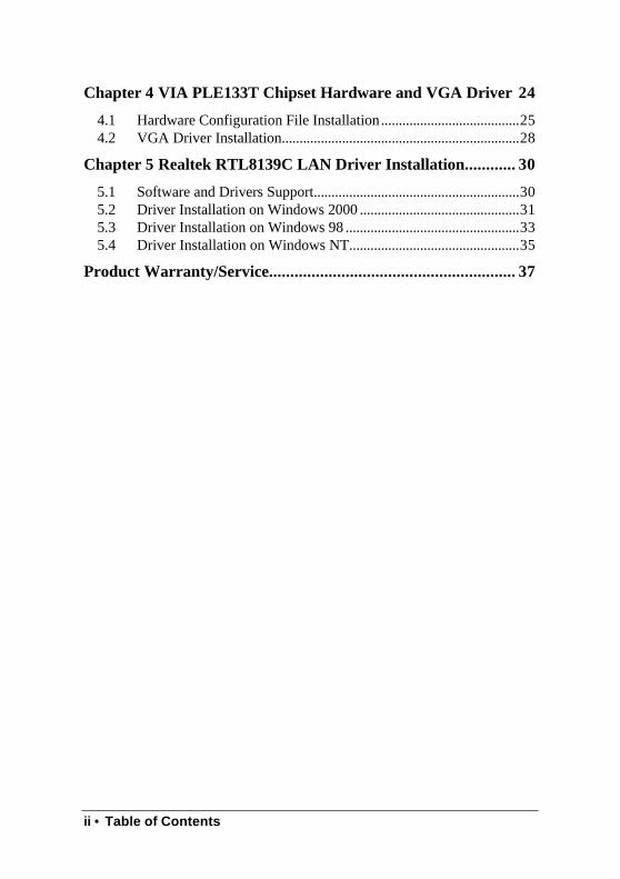
Chapter 4 VIA PLE133T Chipset Hardware and VGA Driver 24
4.1 Hardware Configuration File Installation.......................................25 4.2 VGA Driver Installation...................................................................28
Chapter 5 Realtek RTL8139C LAN Driver Installation............ 30
5.1 Software and Drivers Support..........................................................30 5.2 Driver Installation on Windows 2000 .............................................31 5.3 Driver Installation on Windows 98 .................................................33 5.4 Driver Installation on Windows NT................................................35
Product Warranty/Service.......................................................... 37

How to Use This Guide • iii
How to Use This Guide
This manual is designed to help you to use the NuPRO-760 series.
Chapter 1, “Introduction” gives an overview of the product features and
specifications.
Chapter 2, “Jumpers and Connectors” describes how to install the SBC. The PCB layout, jumper setting and connector pin assignments are shown.
Chapter 3 “Watchdog Programming” shows the functionality of the watchdog timer.
Chapter 4, “VIA PLE133T Hardware and VGA Driver” describes how to install the VGA and Hardware drivers of the VIA PLE133T chipset.
Chapter 5, “Realtek RTL8139C LAN driver installation” describes how to install the LAN driver for NuPRO-760 SBC.

Introduction • 1
1
Introduction
This manual is designed to give you information on the NuPRO-760 series CPU card. The information inside this user’s manual can be applied to NuPRO-760 series if without specified.
The topics covered in this chapter are as follows:
• Checklist
• Description
• Features
• Specifications
• Intelligence
• PCB Layout Drawing
• Mechanical Drawing
2 • Introduction
1.1 Checklist
Please check that your package is complete and contains the items below. If you discover damaged or missing items, please contact your dealer.
• The NuPRO-760 Industrial Computer Main Board
• This User’s Manual
• 1 IDE Ribbon Cable (ATA-100)
• 1 Floppy Ribbon Connector
• 1 Serial Port Ribbon Cable and 1 Parallel Port Cable with bracket
• 1 Serial Port Ribbon Cable with bracket
• 1 CD Containing hardware configuration file, VGA Driver and LAN Driver
1.2 Description
The NuPRO-760 is a single-CPU PICMG form factor, industrial computer mainboard. The NuPRO-760 is based on the Intel PGA370 socket processor with the VIA APOLLO PLE133T and VT82C686B chipset. It accommodates single Intel Pentium III (Coppermine/Tualatin), Celeron and VIA C3 processor. This board supports three DIMM sockets and can accommodates up to 1.5GB SDRAM configuration.
The VIA VT82C686B south bridge is embedded with hardware monitoring device that monitors system and CPU temperature, system voltages, and CPU, chassis fan speeds to prevent system crashes by warning the user of adverse conditions. NuPRO-760 also has a case-open indicator for security.
Introduction • 3
1.3 Features
• Single Pentium III (Coppermine/Tualatin) / Celeron (FC-PGA, FC-PGA2) / VIA C3 processor with auto-selection of core voltages. The Front Side Bus (FSB) frequency can be 66/100/133MHz
• VIA Apollo PLE133T (VT8601T) North Bridge Controller
• VIA VT82C686B super South Bridge Controller
• Up to 1.5GB PC-133 SDRAM system memory (3 x 168-pin DIMM sockets)
• EIDE support up to Ultra/DMA100
• Two RS-232 interface
• One High speed bi-directional SPP/ECP/EPP parallel port
• Two USB ports
• One PS/2 Keyboard port and one PS/2 Mouse port
• Programmable watchdog timer
• Hardware Monitoring
• Single 10/100 Base-T Ethernet interface with external LAN status LED connectors
• AC’97 Link interface support DB-AC97S board for audio input & output
• ISA High Drive 64mA
• Standard ATX power connector on board
• The mounting holes around it to fit the board into chassis without Backplane (When using standard ATX power connector as power source)
4 • Introduction
1.4 Specifications
♦ Processor Socket: Socket-370 connector
♦ Processor: Intel Celeron and Pentium III (FC-PGA & FC-PGA2), VIA C3 CPU
♦ Secondary Cache: built in CPU
♦ Bus Speed: 66/100/133MHz
♦ Chipset: VIA PLE133T (VT8601T + VT82C686B)
♦ Memory Sockets:
• Three 168-pin DIMM sockets
• Max. 1.5GB SDRAM
• Memory type: PC-133 un-buffered SDRAM
♦ Integrated Graphics Controller:
• VIA 8601T built-in Trident 3D AGP 2D/3D graphics engine
• Video memory share with system memory up to 8MB
• AGP 4X, ACPI and VESA compliant
• Embedded 230MHz RAMDAC in chipset
• DDC2B compliant
• Support up to 1600x1200 resolution
♦ BIOS: Award BIOS, support PnP
• DMI BIOS Support: Desktop Management Interface (DMI) allows users to download system hardware-level information such as CPU type, CPU speed, internal/external frequencies and memory size
• Green Function: Power management via BIOS, activated through mouse/keyboard movement
♦ PCI Compliance: Compliant to PCI rev. 2.2 standards, 32bit/33Mhz interface.
♦ PCI Bus Ethernet Interface:
• On-board Realtek RTL8139C high performance IEEE 802.3 10/100-BaseTX Ethernet controller
• Supports IEEE 802.3µ auto-negotiation for 10Base-T/100Base-TX
Introduction • 5
• Supports IEEE 802.3x 100Base-TX flow control
• Reserved with pin-header for Ethernet’s LED for user’s applications
• Support Wake-On-LAN function and remote wake-up
♦ Enhanced IDE: Bus Master IDE controller, two EIDE interfaces support up to four IDE devices, including HDD, LS-120 and ATAPI CD-ROM drives. Support PIO Mode 3/4 and Ultra DMA/33/66/100 IDE devices. Onboard primary and secondary 40-pin IDE port.
♦ Super I/O Chipset: Built-in VIA 82C686B chipset
♦ Parallel Port:
• One high-speed parallel port, SPP/EPP/ECP mode
♦ Serial Port:
• Two 16C550 UART compatible ports with RS-232 interface
♦ FDD Interface: Two floppy drives (360KB, 720KB, 1.2MB, 1.44MB, 2.88MB)
♦ USB Interface: Two USB pin-header connectors, compliant with USB Specification Rev. 1.1, Individual over-current protection
♦ AC’97 Link:
• One 10 pin connector for DB-AC97S audio board
♦ Watchdog Timer:
• Programmable I/O port 440h and 443h to configure watchdog timer
• Time-out timing select 0~255 seconds
♦ Hardware Monitoring:
• Built-in VIA 82C686B, monitoring CPU temperature, CPU fan, system temperature and DC Voltages
♦ Keyboard and Mouse Connectors:
• One PS/2 Keyboard port and one PS/2 Mouse port
• One external 5-pin keyboard connector
♦ Flash Disk Supporting:
• Support flash module DOM2000 (4MB~256MB) or 2.5” flash disk Flash2000 (8MB~2GB) on IDE port
6 • Introduction
• Support DiskOnChip (DOC) up to 288MB
♦ ISA High-drive: ISA bus high driving capability up to 64mA on all address and control lines
♦ Power supply: AT/ATX
♦ Environmental:
• Storage Temperature: -20°C to 80°C
• Operation Temperature: 0°C to 60°C
• Humidity: 5% to 95%
♦ Power Requirement:
Power Type Value (MAX) Unit Note +5V 7400 mA +12V 240 mA 1 –12V 100 mA +5VSB 50 mA 2
1. Without FAN current. 2. When power-off and using ATX power supply
System configuration : NuPRO-760, Intel Pentium III/1GB (133MHz FSB), 1.5GB SDRAM (256MB PC-133 SDRAM x 3).
Note: The above values are the maximum power requirement for SBC with CPU and RAM only, the CPU is running under full loading. The power for all the other peripheral devices such as keyboard, mouse, add-on cards, HDD, or CD ROM is not included.
♦ Dimension: 338mm x 122mm(13.3” x 4.8”). Full-sized
Introduction • 7
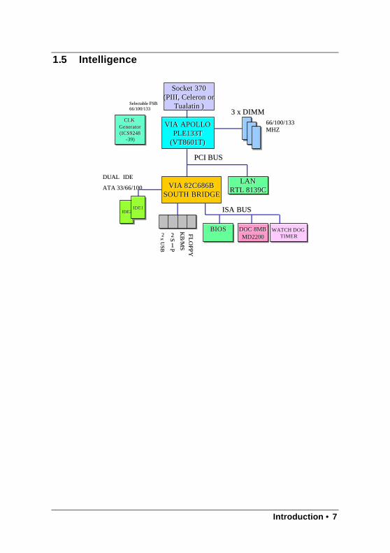
1.5 Intelligence
Socket 370Socket 370(PIII, Celeron or(PIII, Celeron or
Tualatin )Tualatin )
VIA APOLLOVIA APOLLOPLE133TPLE133T
(VT8601T)(VT8601T)
VIA 82C686BVIA 82C686BSOUTH BRIDGESOUTH BRIDGE
PCI BUSPCI BUS
LANRTL 8139C
LANLANRTL 8139CRTL 8139C
IDE2IDE2IDE2IDE1IDE1IDE1
DUAL IDEDUAL IDE
ATA 33/66/100ATA 33/66/100
22x USB
x USB
22SS
11PP
KB
/MS
KB
/MS
FLOPPY
FLO
PPY
ISA BUSISA BUS
BIOSBIOSBIOS DOC 8MBMD2200
DOC 8MBDOC 8MBMD2200MD2200
WATCH DOG TIMER
WATCH DOG WATCH DOG TIMERTIMER
3 3 x DIMMx DIMM66/100/133 66/100/133 MHZMHZ
CLK Generator(ICS9248
-39)
CLK CLK GeneratorGenerator(ICS9248(ICS9248
--39)39)
Selectable FSB Selectable FSB 66/100/13366/100/133
8 • Introduction
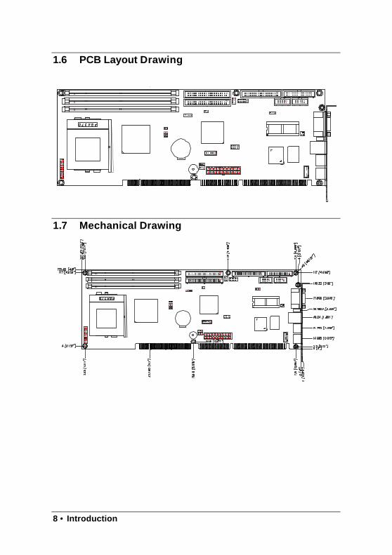
1.6 PCB Layout Drawing
1.7 Mechanical Drawing
Jumpers and Connectors • 9
2
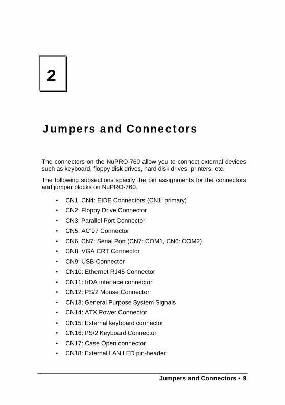
Jumpers and Connectors
The connectors on the NuPRO-760 allow you to connect external devices such as keyboard, floppy disk drives, hard disk drives, printers, etc.
The following subsections specify the pin assignments for the connectors and jumper blocks on NuPRO-760.
• CN1, CN4: EIDE Connectors (CN1: primary)
• CN2: Floppy Drive Connector
• CN3: Parallel Port Connector
• CN5: AC’97 Connector
• CN6, CN7: Serial Port (CN7: COM1, CN6: COM2)
• CN8: VGA CRT Connector
• CN9: USB Connector
• CN10: Ethernet RJ45 Connector
• CN11: IrDA interface connector
• CN12: PS/2 Mouse Connector
• CN13: General Purpose System Signals
• CN14: ATX Power Connector
• CN15: External keyboard connector
• CN16: PS/2 Keyboard Connector
• CN17: Case Open connector
• CN18: External LAN LED pin-header
10 • Jumpers and Connectors
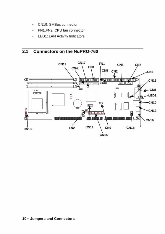
• CN19: SMBus connector
• FN1,FN2: CPU fan connector
• LED1: LAN Activity Indicators
2.1 Connectors on the NuPRO-760
CN8
CN10
CN12
CN16:
CN15:
CN3
CN6
CN9 FN2
CN2
CN11
FN1 CN1 CN4:
LED1
CN7 CN17 CN19
CN18
CN13
CN14
CN5
Jumpers and Connectors • 11
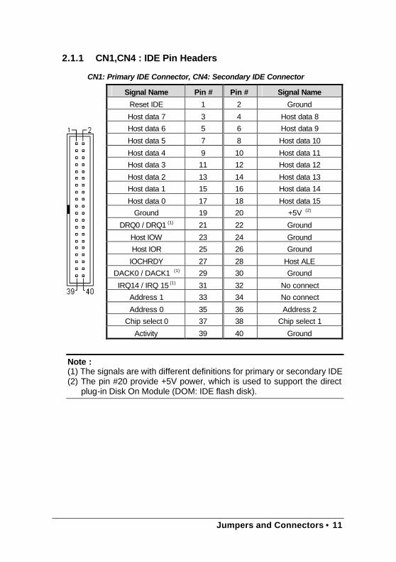
2.1.1 CN1,CN4 : IDE Pin Headers
CN1: Primary IDE Connector, CN4: Secondary IDE Connector
Signal Name Pin # Pin # Signal Name
Reset IDE 1 2 Ground
Host data 7 3 4 Host data 8
Host data 6 5 6 Host data 9
Host data 5 7 8 Host data 10
Host data 4 9 10 Host data 11
Host data 3 11 12 Host data 12
Host data 2 13 14 Host data 13
Host data 1 15 16 Host data 14
Host data 0 17 18 Host data 15
Ground 19 20 +5V (2)
DRQ0 / DRQ1 (1) 21 22 Ground
Host IOW 23 24 Ground
Host IOR 25 26 Ground
IOCHRDY 27 28 Host ALE
DACK0 / DACK1 (1) 29 30 Ground
IRQ14 / IRQ 15 (1) 31 32 No connect
Address 1 33 34 No connect
Address 0 35 36 Address 2
Chip select 0 37 38 Chip select 1
Activity 39 40 Ground
Note : (1) The signals are with different definitions for primary or secondary IDE (2) The pin #20 provide +5V power, which is used to support the direct
plug-in Disk On Module (DOM: IDE flash disk).
12 • Jumpers and Connectors
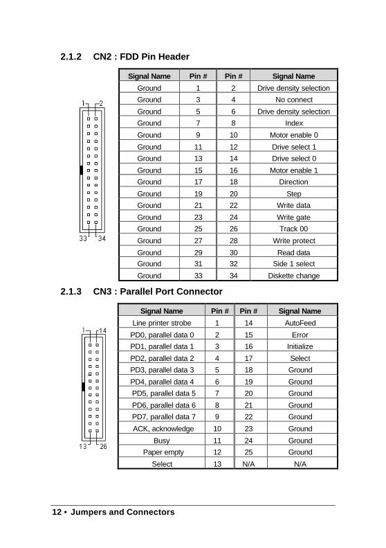
2.1.2 CN2 : FDD Pin Header
Signal Name Pin # Pin # Signal Name
Ground 1 2 Drive density selection
Ground 3 4 No connect
Ground 5 6 Drive density selection
Ground 7 8 Index
Ground 9 10 Motor enable 0
Ground 11 12 Drive select 1
Ground 13 14 Drive select 0
Ground 15 16 Motor enable 1
Ground 17 18 Direction
Ground 19 20 Step
Ground 21 22 Write data
Ground 23 24 Write gate
Ground 25 26 Track 00
Ground 27 28 Write protect
Ground 29 30 Read data Ground 31 32 Side 1 select
Ground 33 34 Diskette change
2.1.3 CN3 : Parallel Port Connector
Signal Name Pin # Pin # Signal Name
Line printer strobe 1 14 AutoFeed
PD0, parallel data 0 2 15 Error
PD1, parallel data 1 3 16 Initialize
PD2, parallel data 2 4 17 Select
PD3, parallel data 3 5 18 Ground
PD4, parallel data 4 6 19 Ground
PD5, parallel data 5 7 20 Ground
PD6, parallel data 6 8 21 Ground
PD7, parallel data 7 9 22 Ground
ACK, acknowledge 10 23 Ground
Busy 11 24 Ground
Paper empty 12 25 Ground
Select 13 N/A N/A
Jumpers and Connectors • 13
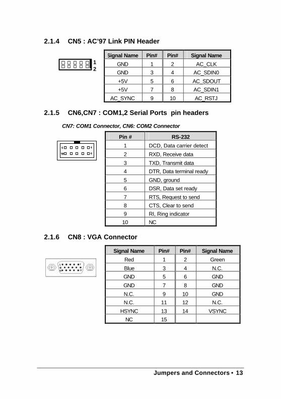
2.1.4 CN5 : AC’97 Link PIN Header
Signal Name Pin# Pin# Signal Name
GND 1 2 AC_CLK
GND 3 4 AC_SDIN0
+5V 5 6 AC_SDOUT
+5V 7 8 AC_SDIN1
AC_SYNC 9 10 AC_RSTJ 2.1.5 CN6,CN7 : COM1,2 Serial Ports pin headers
CN7: COM1 Connector, CN6: COM2 Connector
Pin # RS-232
1 DCD, Data carrier detect
2 RXD, Receive data
3 TXD, Transmit data
4 DTR, Data terminal ready
5 GND, ground
6 DSR, Data set ready
7 RTS, Request to send
8 CTS, Clear to send
9 RI, Ring indicator
10 NC 2.1.6 CN8 : VGA Connector
Signal Name Pin# Pin# Signal Name
Red 1 2 Green
Blue 3 4 N.C.
GND 5 6 GND
GND 7 8 GND
N.C. 9 10 GND
N.C. 11 12 N.C.
HSYNC 13 14 VSYNC
NC 15
1 2
14 • Jumpers and Connectors
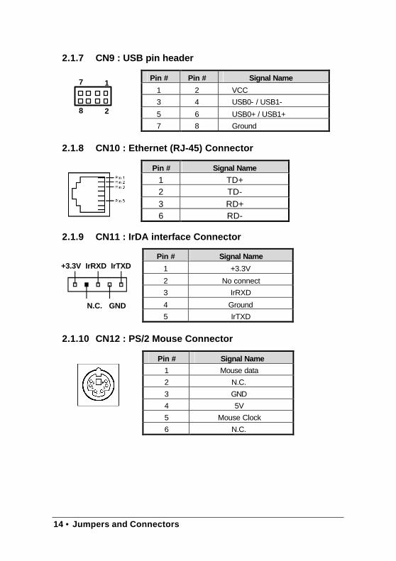
2.1.7 CN9 : USB pin header
Pin # Pin # Signal Name
1 2 VCC
3 4 USB0- / USB1-
5 6 USB0+ / USB1+
7 8 Ground
2.1.8 CN10 : Ethernet (RJ-45) Connector
Pin # Signal Name
1 TD+ 2 TD- 3 RD+
6 RD- 2.1.9 CN11 : IrDA interface Connector
Pin # Signal Name
1 +3.3V
2 No connect
3 IrRXD
4 Ground
+3.3V IrRXD IrTXD
N.C. GND
5 IrTXD
2.1.10 CN12 : PS/2 Mouse Connector
Pin # Signal Name
1 Mouse data
2 N.C.
3 GND
4 5V
5 Mouse Clock
6 N.C.
1
2
7
8
Jumpers and Connectors • 15
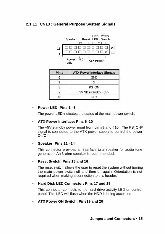
2.1.11 CN13 : General Purpose System Signals
Pin # ATX Power Interface Signals
6 GND
7 X
8 PS_ON
9 5V SB (standby +5V)
10 N.C
• Power LED: Pins 1 - 3
The power LED indicates the status of the main power switch.
• ATX Power Interface: Pins 6 -10
The +5V standby power input from pin #9 and #10. The PS_ON# signal is connected to the ATX power supply to control the power On/Off.
• Speaker: Pins 11 - 14
This connector provides an interface to a speaker for audio tone generation. An 8-ohm speaker is recommended.
• Reset Switch: Pins 15 and 16
The reset switch allows the user to reset the system without turning the main power switch off and then on again. Orientation is not required when making a connection to this header.
• Hard Disk LED Connector: Pins 17 and 18
This connector connects to the hard drive activity LED on control panel. This LED will flash when the HDD is being accessed.
• ATX Power ON Switch: Pins19 and 20
Power LED
+
+
+
1
Speaker Reset HDD LED Power
Switch
N.C
ATX Power
Interface
10
20 11

16 • Jumpers and Connectors
This 2-pin connector is an “ATX Power Supply On/Off Switch” on the system that connects to the power switch on the case. When pressed, the power switch will force the system to power on. When pressed it for 4 seconds, it will force the system to power off.
2.1.12 CN15 : External keyboard connector
1 Pin # Signal Name
1 Keyboard clock
2 Keyboard data
3 NC
4 GND
5 5 Vcc
2.1.13 CN16 : PS/2 Keyboard Connector
Pin # Signal Name
1 Keyboard data
2 N.C.
3 GND
4 5V
5 Keyboard clock
6 N.C.
2.1.14 FAN1,FAN2 : CPU fan connector
FAN1 & 2 are 3-pin header for the CPU and system fan respectively .The fan must be a 12V fan.
Pin # Signal Name
1 Fan speed
2 +12V
3 GND
3 1
Jumpers and Connectors • 17
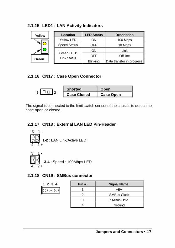
2.1.15 LED1 : LAN Activity Indicators
Location LED Status Description ON 100 Mbps Yellow LED
Speed Status OFF 10 Mbps
ON Link
OFF Off line
Green LED: Link Status
Blinking Data transfer in progress
2.1.16 CN17 : Case Open Connector
Shorted Open Case Closed Case Open
The signal is connected to the limit switch sensor of the chassis to detect the case open or closed.
2.1.17 CN18 : External LAN LED Pin-Header
3 1 -
1-2 : LAN Link/Active LED 4 2 + 3 1 -
3-4 : Speed : 100Mbps LED
4 2 +
2.1.18 CN19 : SMBus connector
Pin # Signal Name
1 +5V
2 SMBus Clock
3 SMBus Data
1 2 3 4
4 Ground
2 1
Green
Yellow
18 • Jumpers and Connectors
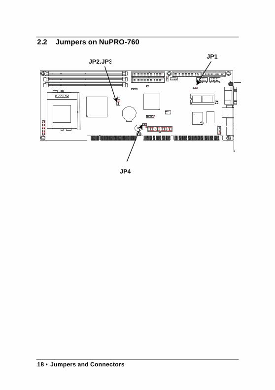
2.2 Jumpers on NuPRO-760
JP2,JP3
JP4
JP1
Jumpers and Connectors • 19
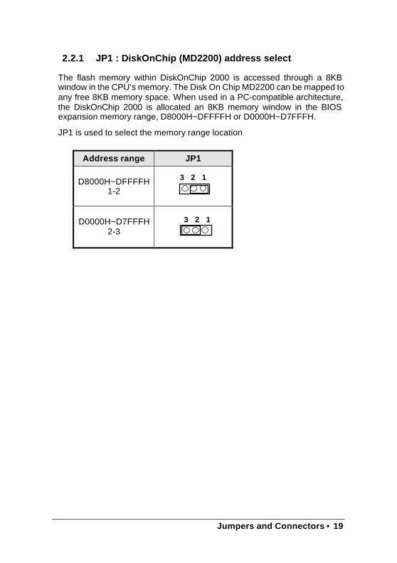
2.2.1 JP1 : DiskOnChip (MD2200) address select
The flash memory within DiskOnChip 2000 is accessed through a 8KB window in the CPU’s memory. The Disk On Chip MD2200 can be mapped to any free 8KB memory space. When used in a PC-compatible architecture, the DiskOnChip 2000 is allocated an 8KB memory window in the BIOS expansion memory range, D8000H~DFFFFH or D0000H~D7FFFH.
JP1 is used to select the memory range location
Address range JP1
D8000H~DFFFFH 1-2
D0000H~D7FFFH 2-3
3 2 1
3 2 1
20 • Jumpers and Connectors
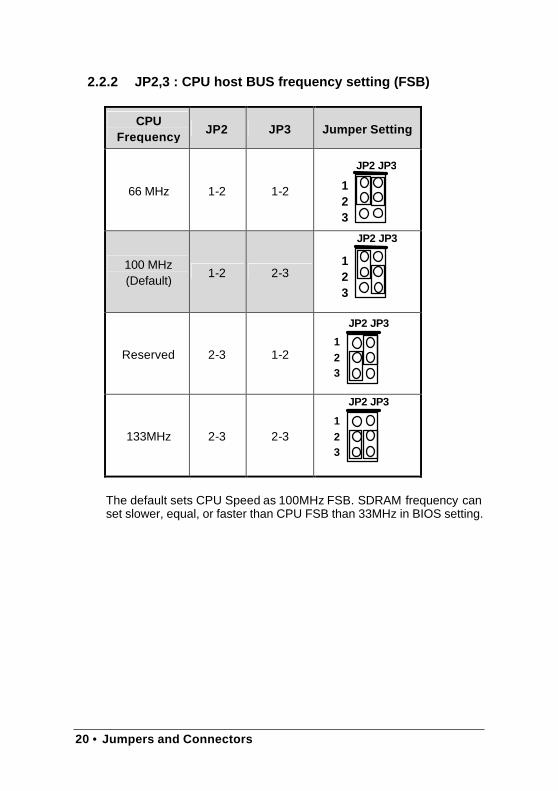
2.2.2 JP2,3 : CPU host BUS frequency setting (FSB)
CPU Frequency
JP2 JP3 Jumper Setting
66 MHz 1-2 1-2
100 MHz (Default)
1-2 2-3
Reserved 2-3 1-2
133MHz 2-3 2-3
The default sets CPU Speed as 100MHz FSB. SDRAM frequency can set slower, equal, or faster than CPU FSB than 33MHz in BIOS setting.
1 2 3
JP2 JP3
1 2 3
JP2 JP3
1 2 3
JP2 JP3
1 2 3
JP2 JP3
Jumpers and Connectors • 21
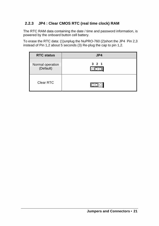
2.2.3 JP4 : Clear CMOS RTC (real time clock) RAM
The RTC RAM data containing the date / time and password information, is powered by the onboard button cell battery.
To erase the RTC data: (1)unplug the NuPRO-760 (2)short the JP4 Pin 2,3 instead of Pin 1,2 about 5 seconds (3) Re-plug the cap to pin 1,2.
RTC status JP4
Normal operation (Default)
Clear RTC
3 2 1

22 • Watchdog Programming Guide
3
Watchdog Programming Guide
The NuPRO-760 implements a watchdog timer by the use of PLD, EPM7032. It contains a one-second resolution down counter. Once setup a value to WDT, the timer begins to count down. The Watchdog output is connected to “reset” button. When the system hangs up without software re-trigger, the system will be reset.
The watchdog timer would reset the system automatically if the system program did not refresh the watchdog timer during the watchdog time out interval. It is set at I/O port 440h and 443h to enable/disable the watchdog time out function. Its clock source 1Hz, and then is divided into 1Hz base to counter a 8 bits counter such that the timer range is from 1 sec to 256 sec with resolution 1 sec.
Regarding to the watchdog function, users must have a program to set the watchdog time out value, and refresh the watchdog timer cycle. If the system programs goes into a dead loop or goes into an abnormal cycle, the watchdog timer cannot be refreshed immediately. Meanwhile, the watchdog timer will reset the system automatically. The watchdog timer will be refreshed by “ disable watchdog output” then “enable watchdog output”.

Watchdog Programming Guide • 23
Watchdog Time Out Table
Timer Value Time Out Time
Value Time Out Time Value Time Out
0 None 8 8sec. . .
1 1sec. 9 9sec. . .
2 2sec. A 10sec. . .
3 3sec. B 11sec. . .
4 4sec. C 12sec. . .
5 5sec. D 13sec. . .
6 6sec. E 14sec. . .
7 7sec. F 15sec. FF 255 sec.
Example :
<Enable Watchdog Timer :>
mov dx , 440h
mov al, <0~255>
out dx,al
<Disable Watchdog Timer :>
Write any Value to I/O port 443h
mov dx, 443h
mov al, <0~255>
out dx, al
24 • VIA PLE133T Chipset Hardware and VGA Driver
4
VIA PLE133T Chipset Hardware and VGA Driver
This chapter describes the installation procedure of VIA Apollo PLE 133T (VIA 8601T) chipset Device Driver for Windows 95/98/2000.
Before installing Windows 95/98/ME onto NuPRO-760, an important issue must be taken care when using maximum size of memory. If a system that is running Windows 95/98/ME contains more than 512 megabytes (for example, 768 megabytes) of physical memory (RAM), you may experience one or more of the following symptoms:
• You may not be able to open an MS-DOS session (or command prompt) while Windows is running. Attempts to do so may generate the following error message: “There is not enough memory available to run this program. Quit one or more programs, and then try again.”
• The computer may stop responding (hang) while Windows is starting, or halt and display the following error message:
“Insufficient memory to initialize windows. Quit one or more memory-resident programs or remove unnecessary utilities from your Config.sys and Autoexec.bat files, and restart your computer.” FInstalling the safe amount (512MB) of memory in your system
(95/98/ME) to avoid the unexpected situation is highly recommended. More detailed information about memory issue, you can refer to the following Microsoft web sites:
http://support.microsoft.com/default.aspx?scid=kb;EN-US;q184447 http://support.microsoft.com/support/kb/articles/Q253/9/12.asp
VIA PLE133T Chipset Hardware and VGA Driver • 25
4.1 Hardware Configuration File Installation
This section describes system requirements of VIA Apollo PLE 133T (VIA 8601T) chipset Device Driver. This driver has been designed for and tested with Windows 98/95.
The system must contain a supported Intel Socket 370 processor and chipset configuration. Ensure that a mouse is connected to the system. One of the following versions of Windows 95/98/2000 must be installed on the system prior to running utility program.
• Windows 2000 : 5.00.2195 (Original release)
• Windows 98 : Second Edition 4.10.2222 A (Original Release)
• Windows 98 : 4.10.1998 (Original Release)
• Windows 95 : 4.00.950c (OSR 2.5 with or without USB Supplement)
• Windows 95 : 4.00.950b (OSR 2.1 with USB Supplement)
• Windows 95 : 4.00.950b (OSR 2.1 with USB Supplement)
• Windows 95 : 4.00.950a (OSR1)
• Windows 95 : 4.00.950 (Original Release)
26 • VIA PLE133T Chipset Hardware and VGA Driver
Installing Hardware Configuration File
This subsection describes how to install the hardware configuration file on a system where Windows 98/95 is installed.
Note: Record the location of the Windows 95/98/2000 directory before installing the driver.
1. Check the System Requirements. Windows 95/98/2000 must be fully installed and running on the system prior to running this software.
2. Close any running applications.
3. The files are stored in an integrated application setup program. This program is designed for a Windows 95/98/2000 program that allows the INF files to be installed.
4. Run the SETUP.EXE program In X:\CHIPDRV\Chipset\VIA_Chip
5. welcome , Click Cancel to quit Setup and then close any programs you have running, Click Next to continue with the Setup program , Click “Next”.
6. VIA Service Pack 1 README, Click Yes means you have read and agreed with the license agreement and README ,Click No to decline and Exit , Click “Yes”.
7. 4in1 Setup Mode Option , Click to enable Normally or Quickly install , Click “Next”.
8. Setup Components , This setup program will install the following drivers , If you don’t want to install them , you can uncheck the associated check box , Click “Next”.
9. VIA PCI IDE Bus Driver 1.20 , install/Uninstall VIA PCI IDE Bus Driver , Click “Next”.
10. VIA_GART AGP Driver 4.05 , Setup program will install/uninstall AGP driver for you , Click “Next”.
11. Setup Complete , Setup has finished copying files to your computer , Before you can use the program , you must restart windows or your computer , Click “ Finish” to restart the system.
VIA PLE133T Chipset Hardware and VGA Driver • 27
12. Follow the screen instructions and use default settings to complete the setup when Windows 95/98/2000 is re-started. Upon re-start, Windows 95/98/2000 will display that it has found many hardware and is installing driver for them. If one New Hardware Found dialog box is displayed requesting the location of the drivers, use the mouse to click on the scrollbar and click on the <Windows 95/98/2000 directory>.
13. Select Yes, when prompted to re-start Windows 95/98/2000.
28 • VIA PLE133T Chipset Hardware and VGA Driver
4.2 VGA Driver Installation
This section provides information on how to install the VGA driver that come in the Compact Disk with the package. Please follow the instructions set forth in this section carefully. Please note that there must be relevant software installed in your system before you could proceed to install the VGA driver.
Installing the Drivers for Windows 98/95 and Win 2000
The following section describes the normal display driver installation procedures for Windows 95/98/2000. Use the following procedures when installing the display drivers for Windows 98/95.
1. The driver is included in the ADLINK CD. Run the SETUP.exe under the following directory: X:\CHIPDRV\VGA\VT8601T\win 9x (or Win 2K folder for Win 2000 installation).
2. Click Next on Welcome Screen to read and agree to the license agreement.
3. Click Yes if you agree to continue. NOTE: If you click No, the program will terminate.
4. Click Yes to restart your computer and for the new settings to take effect.
5. Follow the screen instructions and use default settings to complete the setup when Windows 95/98/2000 is re-started.
Installing the Drivers for Windows NT 4.0
[IMPORTANT]: You should install the Windows NT 4.0 with at least Service Pack 4 (version number: 4.00.1381) first before installing the VGA driver. If you don't have the Windows NT 4.0 Service Pack 4, please contact your software vendor or download it from Microsoft's web site.
The procedures below show you how to install the VGA driver for Windows NT 4.0.
1. Boot Windows NT 4.0.
2. The driver is included in the ADLINK CD. Run the SETUP.exe under the following directory: X:\CHIPDRV\VGA\VT8601T\win nt4
3. Click Next on Welcome Screen to read and agree to the license agreement.
4. Click Yes if you agree to continue. NOTE: If you click No, the program will terminate.
VIA PLE133T Chipset Hardware and VGA Driver • 29
5. Windows NT 4.0 will prompt you to restart computer. Click Yes for the new settings to take effect.
6. Follow the screen instructions and use default settings to complete the setup when Windows NT 4.0 is re-started.
30 • Realtek 8139C LAN Driver Installation
5
Realtek RTL8139C LAN Driver
Installation
This chapter describes LAN driver installation for the onboard Ethernet controller RTL8139C. The relative drivers are under the following ADLINK CD directory: X:\CHIPDRV\LAN\RTL8139c, where X: is the location of the CD-ROM drive.
5.1 Software and Drivers Support
The RTL8139C drivers support the following OS or platforms: Windows 98, Windows ME, Windows 2000, Windows NT.
All the above drivers are included in the ADLINK CD. In the following section, we will describe the driver installation for Windows 98, Windows 2000, and Windows NT. For the driver installation of the other OS, please refer the readme.txt file inside the CD.
Realtek 8139C LAN Driver Installation • 31
5.2 Driver Installation on Windows 2000
The Windows 2000 may install the LAN driver. We recommend you to manually installed the most updated LAN driver, which shipped with ADLINK CD to guarantee the compatibility. After installing the Windows 2000, please update the new drivers by the following procedures.
1. Boot Windows 2000, Click Start. Select Settings then double-click
the Control Panel.
2. Double-click System icon, click Hardware tab, click Device
Manager button.
3. Double-click Network Adapters entry,Double-click the Realtek RTL
8139 PCI Fast Ethernet Adapter entry.
4. Click Driver tab, then click Update Driver… button.
5. An Upgrade Device Driver Wizard windows, click Next>.
6. Select Display a list of ... and click Next>. The next window may
show a list of hardware models.
7. Insert the CD and click Have Disk.
8. Browse the RTL-8139C driver in the following path: X:\
CHIPDRV\LAN\RTL8139c\WINDOWS\Win2k\, highlight
Netrts5.inf, click Open, then click OK.
9. Highlight the model: Realtek RTL8139 PCI Fast Ethernet
Adapter, then click NEXT>. An Update Driver Warning window may
pop up, click Yes to continue.

32 • Realtek 8139C LAN Driver Installation
10. Click NEXT> button, then the Wizard summary window appears.
11. Click Finish button, then click CLOSE button.
Realtek 8139C LAN Driver Installation • 33
5.3 Driver Installation on Windows 98
The Windows 98 will install the LAN driver automatically. We recommend you to manually updated the LAN, which on the ADLINK CD to guarantee the compatibility. After installing Windows 98, please update the new drivers by the following procedures.
1. Boot Windows 98, Click Start. Select Settings then double-click
the Control Panel.
2. Double-click on the System icon, click on the Device Manager tab.
3. Double-click on the Network Adapters entry,. Click the
Properties.
4. Click on the Driver button, then click Update Driver…button.
5. Update Device Driver Wizard starts, click NEXT.
6. Select Display a list of ... and click NEXT. The next window allows
the user to specify a specific path. Insert the CD and click Have
Disk.
7. Browse the RTL-8139 driver in the following path:
X:\ CHIPDRV\LAN\RTL8139c\WINDOWS\Win98 highlight NETRTS5.INF, click OK. The Update Wizard displays the message that it has found the driver. Click OK again to update the driver.
Note: Windows 98 may ask you to insert the original Windows 98 CD to
install the LAN protocols.
8. Click NEXT button, then the Wizard summary window appears.

34 • Realtek 8139C LAN Driver Installation
9. Click Finish button, then restart the computer to active the new
driver.
Realtek 8139C LAN Driver Installation • 35
5.4 Driver Installation on Windows NT
Before install the LAN driver on Windows NT, please copy the LAN driver in the CD to a floppy diskette. You have to put a new disk into drive A, then type the following batch command under DOS environment to copy the relative NT drivers.
X: \CHIPDRV\LAN\RTL8139c\WINDOWS\NT4.0
where X is the CD-ROM drive.
Windows NT may ask to installs a LAN driver from its own library of drivers. We recommend you to manually update the LAN, which on the ADLINK CD to guarantee the compatibility. After installing Windows NT, please update the new driver by the following procedures.
1. From the Control Panel, double-click the Network icon, a Network
Configuration window pop up, click Yes.
2. In Network Setup Wizard, click Next>, click Select From List…
button.
3. Copy all files in the directory:
X:\CHIPDRV\LAN\RTL8139c\WINDOWS\NT4.0 to floppy d iskette.
4. Insert LAN driver floppy diskette into A drive and click Have Disk.
5. In the dialog box of Insert Disk window, type in A:, Click OK.
6. A Select OEM Option window pop up, click OK, then click Next>.
7. Select necessary Network Protocols, click Next>.
8. Select necessary Network Services, click Next>.
9. Click Next> until Window NT Setup dialog box pop up. Type in
X:\i386 in the dialog box, then insert the original Windows NT CD,
and click Continue.

36 • Realtek 8139C LAN Driver Installation
10. Then click OK until the setup completed.
11. Restart the computer to reboot.

Product Warranty Service • 37
Product Warranty/Service
ADLINK warrants that equipment furnished will be free from defects in material and workmanship for a period of one year from the date of shipment. during the warranty period, we shall, at our option, either repair or replace any product that proves to be defective under normal operation.
This warranty shall not apply to equipment that has been previously repaired or altered outside our plant in any way as to, in the judgment of the manufacturer, affect its reliability. Nor will it apply if the equipment has been used in a manner exceeding its specifications or if the serial number has been removed.
ADLINK does not assume any liability for consequential damages as a result from our product uses, and in any event our liability shall not exceed the original selling price of the equipment. The remedies provided herein are the customer’s sole and exclusive remedies. In no event shall ADLINK be liable for direct, indirect, special or consequential damages whether based on contract of any other legal theory.
The equipment must be returned postage-prepaid. Package it securely and insure it. You will be charged for parts and labor if the warranty period is expired or the product is proves to be misuse, abuse or unauthorized repair or modification.