Fully Differential Amplifiers - 3 TIPL 2023 TI Precision Labs: Op Amps Prepared and Presented by Samir Cherian
Fully Differential Amplifiers - 3 - TI.com · Fully Differential Amplifiers - 3 ... Hello and welcome to part 3 of the fully differential amplifier ... An FDAs open-loop gain is the
Hello and welcome to part 3 of the fully differential amplifier series. In this video we will analyze an FDAs open-loop gain and noise gain and how these factors affect the amplifiers stability. We will also study how to simulate these parameters in SPICE using TINA-TI.
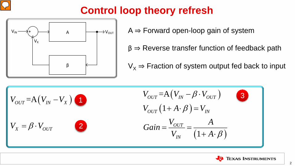
Control loop theory refresh
2
( )=AOUT IN X
X OUT
V V V
V Vβ
−
= ⋅
β
AVIN VOUT+¯
VX
A ⇒ Forward open-loop gain of system β ⇒ Reverse transfer function of feedback path VX ⇒ Fraction of system output fed back to input
( )( )
( )
=A
1
1
OUT IN OUT
OUT IN
OUT
IN
V V V
V A VV AGainV A
β
β
β
− ⋅
+ ⋅ =
= =+ ⋅
1
2
3
Presenter
Presentation Notes
We will begin with a brief refresh of control loop theory. The generic design of a negative feedback loop for a control system is shown here. “A“ represents the systems open-loop gain in the forward direction, while β represents the reverse transfer function of the feedback path. Vin and Vout are the systems input and output respectively while Vx is the fraction of the system output that is fed back to its input. Equation 1 can be derived by observing the systems forward transfer function and is simply the definition of “A”. Equation 2, is derived by observing the systems reverse transfer function and once again is simply the definition of “β”. Substituting the value of Vx from equation 2 back into equation 1, we get equation 3 which after further simplification gives the systems closed-loop gain. We will next see how this model can be applied to a fully-differential amplifier.
A and A are the amplifiers open and closed-loop gain respectively,1 is the Feedback factor (AND) is the Noise Gain.
OLCL
OL
OL CL
AAA β
ββ
=+
Presenter
Presentation Notes
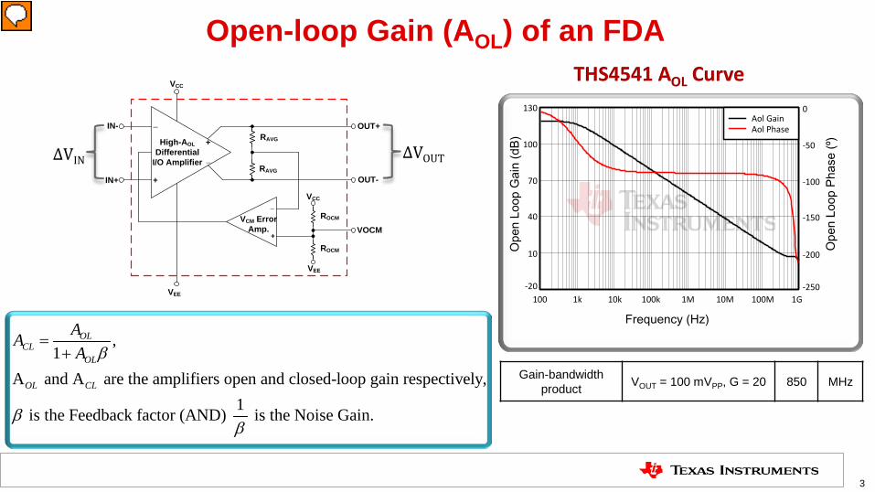
The open-loop gain or Aol of any Amplifier is the ratio of its differential output to its differential input when no feedback is applied. An FDAs open-loop gain is the gain of the feedforward amplifier. Just like an ideal opamp, an ideal FDA will have infinite open-loop gain across an infinite bandwidth. The open-loop gain and phase curves of the THS4541 are shown here. It has a very high AOL at low frequencies, which decreases at 20 dB/decade after the dominant pole. Gain bandwidth product is a vital figure of merit of an amplifiers speed. The faster an amplifier the higher its gain bandwidth product. An amplifier’s gain-bandwidth product can be estimated from its open-loop gain curve by measuring the AOL at high gains. In this case the AOL measures around 8.5 MHz at a gain of 40dB resulting in a gain-bandwidth product of 850 MHz. The higher the AOL at any given frequency the more ideal the amplifier behaves. It is for this reason that a high-precision ADC with a 1MSPS sampling rate should be driven by an amplifier with a bandwidth of at least 10x-100x the sampling rate. Other factors remaining constant, decreased open-loop gain leads directly to an increase in an amplifiers non-linearity and distortion. The control theory equations from the previous slide are repeated here. The forward gain of the system, ’A’ has been replaced by the feedforward amplifiers open-loop gain. The amplifier’s feedback factor, β will be discussed on the subsequent slide. Similar to single-ended opamps the inverse of the amplifier’s feedback factor or 1/β is called the noise gain. The term AOL* β is called the loop gain and is an important factor when determining the phase margin and the stability of the op-amp or FDA.
Signal Gain vs. Noise Gain
4
VCC
VOCM
VEE
RG
RG
RF
RF
VOUT+
VOUT-
FullyDifferentialAmplifier
+
+
¯
¯
RG RFVOUT
VIN
β = RG/(RF+RG)
1, As , .1
Loop Gain. Frequency @ which = 1, is the ( ) -3dB BW
OLCL OL CL
OL
OL
OL CL
AA A AA
AA A
β ββ
β
= →∞ =+→
Signal Gain F
G
RR
= −
Noise Gain
1Noise Gain = Feedback Factor
1
Signal Gain Noise Gain
1 F
G
RRβ
≠
= = +
Presenter
Presentation Notes
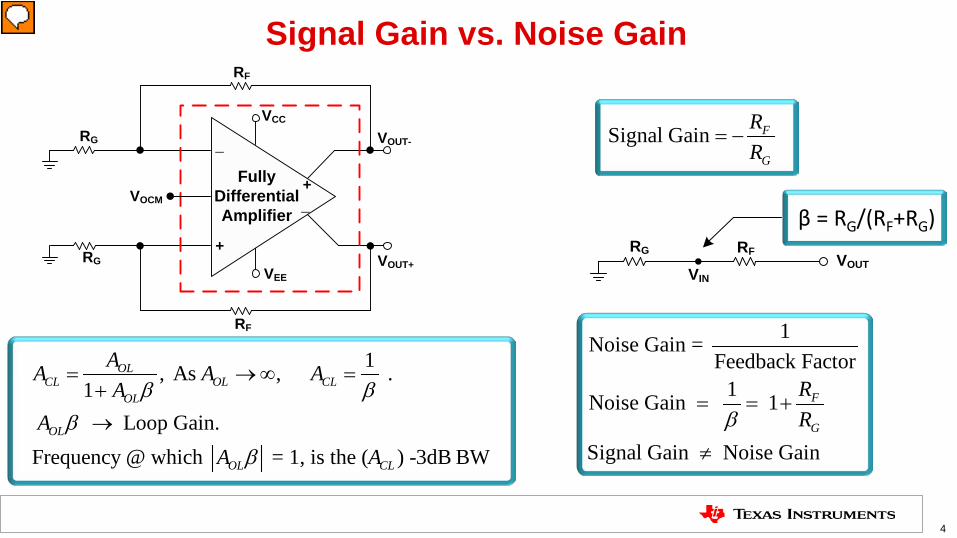
An amplifiers signal gain is defined as the ratio of the magnitude of its output signal to its input signal. An FDAs signal gain is equal to the ratio of its feedback resistance, Rf to its gain resistance Rg. The feedback factor is calculated by finding the fraction of the output signal that is fed back to the amplifier’s input. In the case of a balanced FDA, the feedback factors for each half of the differential amplifier are equal. The feedback factor is then calculated using simple resistor-divider math as shown here. An amplifiers noise gain is the inverse of the feedback factor, or 1 over β . The noise gain for the FDA configuration shown here is thus 1 + Rf /Rg. This scenario is similar to an inverting op-amp where the signal gain is –Rf/Rg and the noise gain is (1 + Rf/Rg). An FDA in a signal gain of 1, where Rf = Rg will be in a noise gain of 2. The term AOL* β is called the loop gain and is an important factor when determining the phase margin and the stability of the op-amp or FDA. Notice that the frequency at which the magnitude of the loop gain equals 1 is the -3dB bandwidth of the amplifier.
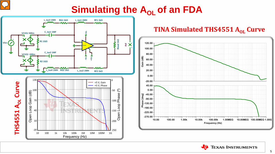
Simulating the AOL of an FDA
5
+5 V, Gain+5 V, Phase
Ope
n Lo
op P
hase
(⁰)
Frequency (Hz)100 1k 10k 100k 1M 10M 100M 1G
-20
10
40
70
100
130
-250
-200
-150
-100
-50
0
Ope
n Lo
op G
ain
(dB)
10
TINA Simulated THS4551 AOL Curve
THS4
551
A OL C
urve
VSrc
VCVS1 500m
VCVS2 -500m
R1 1GΩ
R2 1GΩ
C_Iso1 1MF
C_Iso2 1MF
RG1 1kΩ
RG2 1kΩ
L_Iso3 1MH L_Iso1 1MH RF1 1kΩ
RF2 1kΩ L_Iso2 1MHL_Iso4 1MH
Rloa
d 1k
Ω
Aol
-Vs
+Vs
+Vs
Presenter
Presentation Notes
A SPICE simulator, such as TINA-TI is very useful in determining an amplifiers stability. In order to properly simulate circuits, it is important to be able to extract the parameters that affect it. The main factors affecting amplifier stability are: The open-loop gain, or Aol The feedback factor, β, and The amplifiers open-loop output impedance typically represented by Zol. We will now briefly discuss how to extract some of these parameters from the amplifiers SPICE macromodel. The circuit shown here is used to extract the AOL of an FDA. The THS4551 has been used in this example. The sub-circuit shown here is used to convert the single-ended input to a differential output. The method used to extract the AOL of an FDA is very similar to that used for single-ended op-amps. The large-value inductors create a stable closed-loop circuit at DC, which is necessary for the simulator to converge on a stable operating point. The inductors become open at frequencies greater than a few Hz which is what allows the amplifier to be simulated in an open-loop environment. The capacitors on the other hand are open at DC but become a short at frequencies greater than a few Hz. This configuration allows the differential source to directly drive the amplifier’s inputs. Note that the large inductors and capacitors used in this circuit are only feasible in a simulation environment and cannot be realized practically. Since the feedback loop is open and the source directly drives the inputs, the signal measured at the output is simply the input signal multiplied by the open-loop gain of the amplifier. Running an AC frequency-response analysis directly gives the amplifier’s open-loop magnitude and phase, shown here. The simulated results match the datasheet graph closely. Ignore the low frequency behavior of the simulated response. It is an artifact of the model and doesn’t affect the amplifier performance above a few hundred Hz.
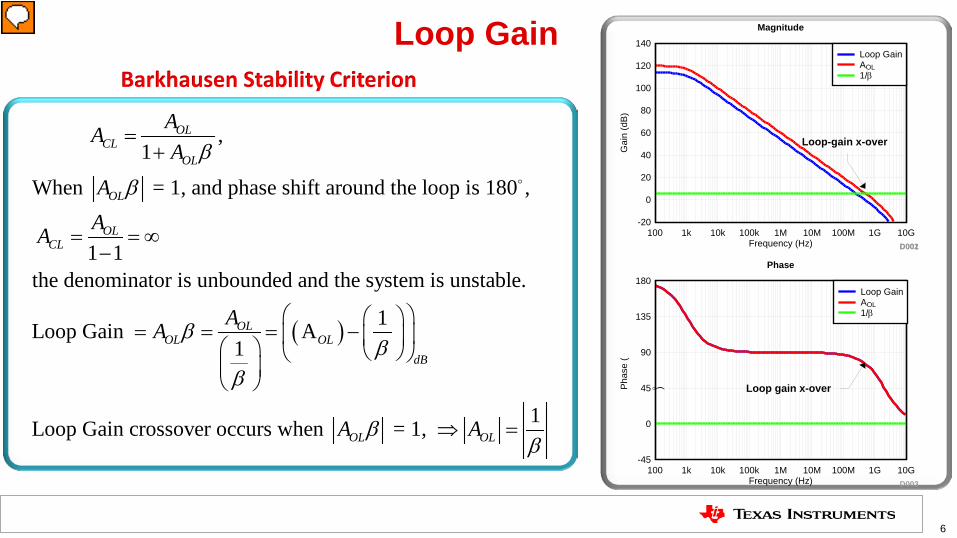
Loop Gain
6
( )
, 1
When = 1, and phase shift around the loop is 180 ,
1 1
the denominator is unbounded and the system is unstable.
1Loop Gain A1
OLCL
OL
OL
OLCL
OLOL OL
dB
AAA
AAA
AA
β
β
ββ
β
=+
= = ∞−
= = = −
1Loop Gain crossover occurs when = 1, OL OLA Aββ
⇒ =
Barkhausen Stability Criterion
Frequency (Hz)
Gai
n (d
B)
Magnitude
-20
0
20
40
60
80
100
120
140
100 1k 10k 100k 1M 10M 100M 1G 10GD001D002
Loop-gain x-over
-
Loop GainAOL1/β
Frequency (Hz)
Pha
se (
° )
Phase
-45
0
45
90
135
180
100 1k 10k 100k 1M 10M 100M 1G 10GD003
-
Loop gain x-over
Loop GainAOL1/β
Presenter
Presentation Notes
We will now study the loop gain of an amplifier and learn why it is vital in determining an amplifiers stability. The closed-loop transfer function of an amplifier is repeated here. When the magnitude of the loop gain equals one and its phase shift is 180 degrees, the denominator becomes zero, and the loop is thus unstable. The loop gain is best analyzed with the help of Bode plots. The open-loop gain of an amplifier is shown here in red. The amplifiers low frequency AOL is 120dB, and it has a dominant pole at 1kHz with a second non-dominant pole at 2 GHz. The amplifier is configured in a signal gain of 1, which in the case of an FDA is a noise gain of 2 or 6dB.The noise gain is shown here in green. The noise gain is purely resistive so there is no phase change across frequency. The loop gain, shown in blue, is the difference between the AOL and 1/β curves. The equation relating Loop gain in the linear domain to Aol and 1/β on a dB scale is shown here. The intersection between the AOL and noise-gain curves is called the loop-gain crossover point and is the frequency at which the loop-gain magnitude becomes 1. The phase is then measured at the loop-gain crossover frequency. The phase-margin is the difference between the measured phase and 180 degrees. For a Butterworth response, the phase margin is 64 degrees. The closer the phase margin is to zero degrees the less stable the amplifier.
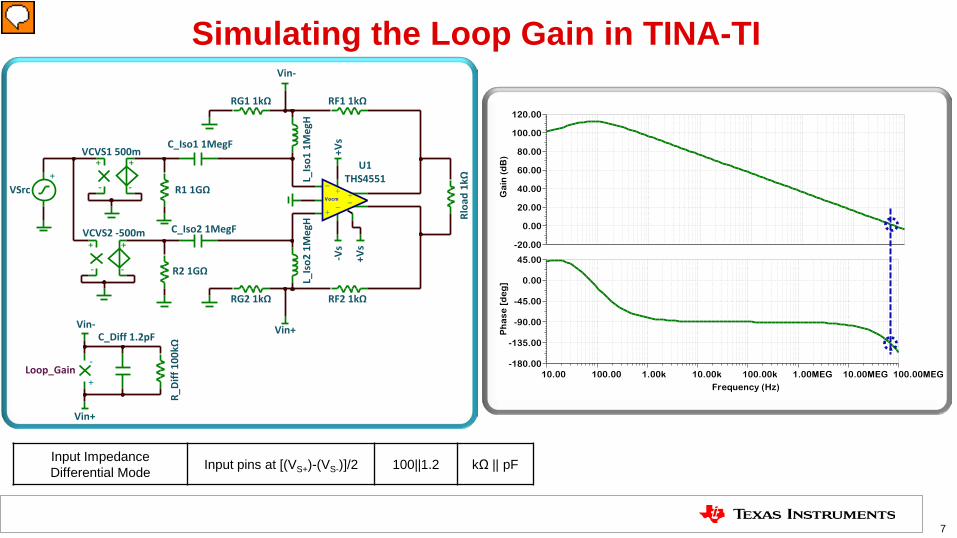
Here I demonstrate how to simulate the loop gain of a fully-differential amplifier using TINA-TI. The TINA circuit set-up to measure the loop gain of the THS4551 in a signal gain of 1 is shown here. An amplifier’s output impedance will interact with the output load which in turn affects its open-loop gain so it is important to include the output load in the loop gain simulation as shown here. At DC, the isolation inductors are a short and the capacitors are an open, allowing the simulator to converge on a stable operating point in a closed-loop configuration. When setting up a simulation using large series capacitors, ensure that all nodes connected to the capacitor have a path to GND to allow the simulator to converge on a stable operating point. The two 1 GΩ resistors serve this purpose and ensure that the two voltage-controlled voltage sources have a finite path to GND. At frequencies greater than a few Hz, the isolation capacitors will act as a short circuit, and the inductors will act as an open circuit thereby opening up the amplifier loop. The differential signal measured at the amplifier output is the amplifier’s open-loop gain. A fraction of the output signal is fed back to the amplifier inputs through the feedback and gain resistors. The signal measured between nodes Vin+ and Vin- is the amplifier’s differential loop gain. R_Diff and C_Diff are the amplifier’s differential input impedance specified in the datasheet, and reinserted here since the inductors isolate the feedback loop from the amplifier’s actual inputs. The amplifier’s input impedance will affect its loop gain and therefore should be included back into the simulation. The loop-gain crossover point is the frequency where the loop-gain magnitude equals 0 dB and occurs at 65 MHz in this circuit configuration. The phase at 65 MHz is measured and then subtracted from 180 degrees to find the phase margin. The simulated phase margin of the circuit is 45 degrees. This method of analyzing the loop gain is critical when designing circuits.
THS4551 AOL Curve
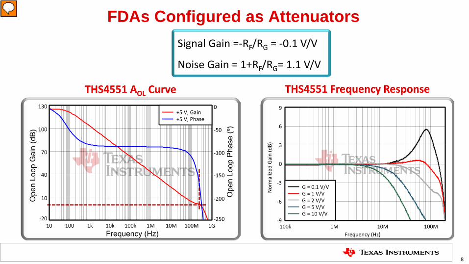
FDAs Configured as Attenuators
8
Signal Gain =-RF/RG = -0.1 V/V
Noise Gain = 1+RF/RG= 1.1 V/V
Frequency (Hz)
Nor
mal
ized
Gain
(dB)
-9
-6
-3
0
3
100k
G = 0.1 V/VG = 1 V/VG = 2 V/VG = 5 V/VG = 10 V/V
6
9
1M 10M 100M
THS4551 Frequency Response
+5 V, Gain+5 V, Phase
Ope
n Lo
op P
hase
(⁰)
Frequency (Hz)100 1k 10k 100k 1M 10M 100M 1G
-20
10
40
70
100
130
-250
-200
-150
-100
-50
0
Ope
n Lo
op G
ain
(dB)
10
Presenter
Presentation Notes
Similar to an inverting amplifier a fully-differential amplifier may be configured as an attenuator when Rg is greater than Rf. In such scenarios the noise gain is still greater than one, since noise gain is equal to 1 + Rf/Rg. Many wideband amplifiers have secondary nondominant poles very close to the point where the AOL curve crosses 0 dB. Such amplifiers will have very low phase margin when configured in low gains or as attenuators. The AOL response of the THS4551 exhibits this behavior as shown here. The THS4551’s loop gain response shows that it has a phase margin close to 0 degrees when configured in a noise gain of 0dB. One way of estimating an amplifier’s phase margin in any gain configuration is by checking the amount of peaking in its small signal frequency response. As expected the THS4551 shows almost 6dB of peaking when configured as an attenuator in a gain of 0.1. Frequency-response peaking exceeding 3dB indicates a phase margin less than 42 degrees and should generally be avoided.
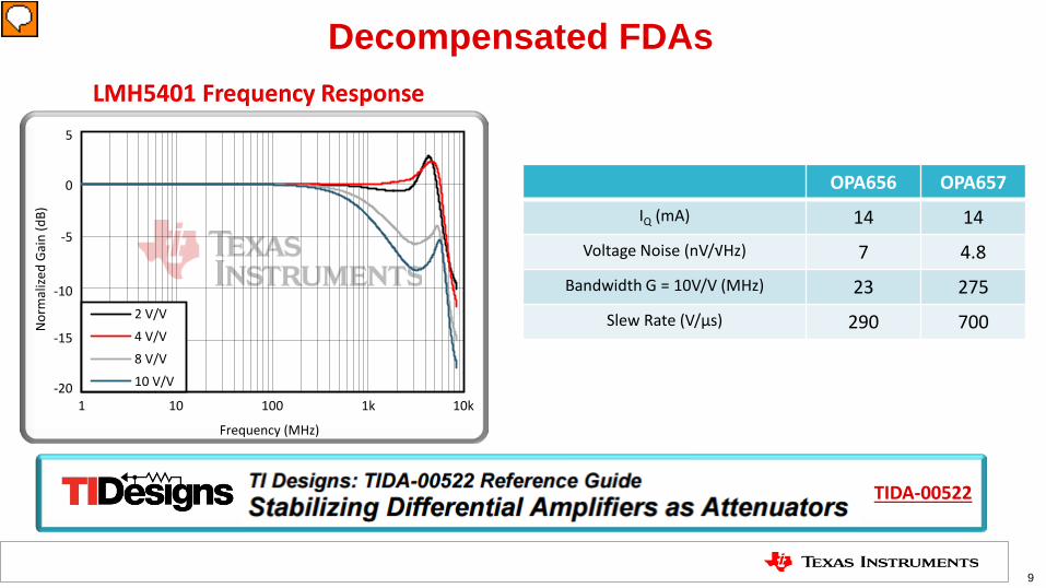
Decompensated FDAs
9
LMH5401 Frequency Response
1
5
Nor
mal
ized
Gain
(dB)
Frequency (MHz)
2 V/V4 V/V8 V/V10 V/V
10 100 1k 10k
0
-5
-10
-15
-20
OPA656 OPA657
IQ (mA) 14 14
Voltage Noise (nV/√Hz) 7 4.8
Bandwidth G = 10V/V (MHz) 23 275
Slew Rate (V/μs) 290 700
TIDA-00522
Presenter
Presentation Notes
Some amplifiers are inherently designed to be stable only in higher gains. Such amplifiers are called decompensated amplifiers. Both single-ended and fully-differential amplifiers may be designed as decompensated amplifiers. The LMH5401 is one such example of a decompensated FDA. It is designed to be used in a linear gain of 4 or higher. The small signal frequency response of the LMH5401 is shown here. Notice that there is about 2.5dB of peaking in a gain of 4. Lower gains will have higher peaking and thus lower phase margin. While the LMH5401 is designed to be stable in a gain of 4 or above, it can be used in lower gain configurations without compromising the phase margin. A technique knows as noise-gain shaping is commonly used when operating a decompensated amplifier in low gains or in attenuator configurations. See Reference design TIDA-00522 to learn how to configure decompensated amplifiers such as the LMH5401 in gains lower than that specified in the datasheet. At this point one may ask, what are the benefits of a decompensated amplifier? A decompensated amplifier can achieve better dynamic performance without consuming any extra power, avoiding the typical amplifier design trade-off between power and bandwidth. For example, the OPA656 and OPA657 are both built on the same process and share the same core design; however, the OPA656 is unity-gain stable while the OPA657 is stable in gains of 7 or higher. Notice that while both amplifiers consume the same quiescent current, the OPA657 has superior bandwidth, noise and slew-rate compared to the OPA656.