Embed Size (px)
Citation preview

FULL PAPERwww.afm-journal.de
© 2018 WILEY-VCH Verlag GmbH & Co. KGaA, Weinheim1802989 (1 of 9)
Fully Elastic and Metal-Free Tactile Sensors for Detecting both Normal and Tangential Forces Based on Triboelectric Nanogenerators
Zewei Ren, Jinhui Nie, Jiajia Shao, Qingsong Lai, Longfei Wang, Jian Chen, Xiangyu Chen,* and Zhong Lin Wang*
A tactile sensor should be able to detect both normal and tangential forces, which is mandatory for simulating human hands, but this fundamental function has been overlooked by most of the previous studies. Here, based on a triboelectric nanogenerator (TENG) with single-electrode mode, the fully elastic and metal-free tactile sensor that can detect both normal and tangential forces is proposed. With tiny burr arrays on the contact interface to facilitate the elastic deformation, the detected normal pressure by the device can reach to 1.5 MPa with a sensitivity of about 51.43 kPa V−1, and a large range of tangential forces can be detected ranging from 0.5 to 40 N with rough sensitivity of 0.83 N V−1 (0.5–3 N) and 2.50 N V−1 (3–40 N). Meanwhile, the applied tangential forces from different directions can also be clearly distinguished by the four-partitioned electrode structure. Moreover, a shield film is coated on the top surface of the device, which can screen the electrostatic interference and enhance the repeatability of the device. The demonstrated concept of this self-powered tactile sensor has excellent applicability for industrial robotics, human–machine interactions, artificial intelligence, etc.
DOI: 10.1002/adfm.201802989
Z. Ren, J. Nie, J. Shao, Q. Lai, L. Wang, J. Chen, Prof. X. Chen, Prof. Z. L. WangBeijing Institute of Nanoenergy and NanosystemsChinese Academy of SciencesBeijing 100083, ChinaE-mail: [email protected]; [email protected]. Ren, J. Nie, J. Shao, Q. Lai, L. Wang, J. Chen, Prof. X. Chen, Prof. Z. L. WangSchool of Nanoscience and TechnologyUniversity of Chinese Academy of SciencesBeijing 100049, ChinaProf. Z. L. WangSchool of Material Science and EngineeringGeorgia Institute of TechnologyAtlanta, GA 30332-0245, USA
The ORCID identification number(s) for the author(s) of this article can be found under https://doi.org/10.1002/adfm.201802989.
artificial intelligence, industrial automa-tion, and health care.[1–3] For the study of tactile sensors, great efforts have been made to further enhance the sensitivity and mechanical flexibility of the device, in order to achieve real progress on cus-tomized feature. To address these require-ments, several physical effects such as capacitive approaches, piezoresistivity, and piezoelectricity have been selected as the transduction mechanism for the tactile sensor design[4–6] and various strain sen-sitive materials have also been intensively developed to fabricate the devices.[7–10] For capacitive and piezoresistive sen-sors, the requirement for external power supply can be a restriction for their appli-cations.[11,12] Meanwhile, although the piezoelectric sensors have self-powered characteristic, the electrical output is too low to achieve a large detection range.[13,14] Recently, another technology, triboelectric nanogenerator (TENG) has been verified
as a promising approach to realize a sensing device with both self-powered capability and high sensitivity.[15–21] The working principle of TENG is based on the coupling effect of triboelec-trification and electrostatic induction. Triboelectrification can generate a high output voltage and electrostatic induction can amplify the reaction signal to the mechanical motion, both of which can improve the sensitivity of the sensor device. In the past few years, lots of touch and pressure sensors based on TENG techniques have been developed.[22–27] However, the applied contact forces on the sensor can be either along the normal direction to the sensor interface, or in the tangential direction. In practice, a device should be able to detect both kinds of forces simultaneously, but this fundamental func-tion has been overlooked by most of the previous studies.[28–34] Hence, it is necessary to design a TENG-based tactile sensor that can measure both normal and tangential forces applied on the device, which can further promote the practical applications of TENG technique in the fields of industrial robotics, human–machine interactions, etc.
In this study, we have demonstrated a self-powered tactile sensor based on pure elastomeric materials that can detect both normal and tangential forces. The TENG with single-elec-trode mode has been employed as the core element for signal
Tactile Sensors
1. Introduction
Flexible and stretchable tactile sensors have attracted notable research interests and a variety of applications have been devel-oped in many fields, including robotics, security monitoring,
Adv. Funct. Mater. 2018, 1802989

www.afm-journal.dewww.advancedsciencenews.com
1802989 (2 of 9) © 2018 WILEY-VCH Verlag GmbH & Co. KGaA, Weinheim
generation, in which the elastic film made of polydimethylsi-loxane (PDMS) is the dielectric material for triboelectrification and the stretchable electrodes are made by mixing PDMS and carbon black (PDMS–CB). Tiny burr arrays are printed on the interface for contact electrification and different voltage signals can be generated from elastic deformation of tiny burr arrays and the dielectric film. By increasing the force applied on the device, two different deformation processes can occur with tiny burr arrays on the contact interface and the dielectric film, which can help us to detect both small and large stresses. The designed tactile sensor not only can detect both normal and tangential forces, but also can distinguish the direction of applied tangential forces. Moreover, a shield film has been coated on the top surface of the sensor, which can screen the electrostatic interference and thus guarantee the stability and repeatability of the sensor. For perspective, this TENG-based sensor can be potentially applied in many fields such as industrial robotics, human–machine interactions and may promote practical study of tactile sensors.
2. Results and Discussion
2.1. The Self-Powered Sensor for Detecting Normal Force
First, we have prepared a sensor device only for detecting the normal force, in order to demonstrate the design concept and
technical method proposed in this work. The detailed structure design and the components of the prepared sensor are shown in Figure 1a. In order to expand the sensing range and increase the sensitivity of the sensor, tiny burr arrays are printed on the surface of both PDMS and PDMS–CB films, as shown in Figure 1a. Micromorphology of the tiny burrs is shown in Figure S1a–c (Supporting Information). A spacer is placed between two films, the materials of which can be polymethyl methacrylate (PMMA) or PDMS. Meanwhile, a highly conduc-tive shield film (see the Experimental Section) is coated on the top surface of the whole sensor. The shield film is grounded in order to screen the electrostatic interference and photograph of the device can be seen in Figure 1d. Scanning electron micro-scopy (SEM) images of micromorphology of PDMS–CB film and PDMS film are shown in Figure 1b,c, respectively. The mixing of PDMS and CB leads to rough surface in the microscale, which is favorable for enhancing the contact electrification of TENG. Figure 1e shows the elastic properties of PDMS–CB and original PDMS materials, where the strain changes of two kinds of materials in response to variable tensile strength are almost the same. The result indicates that the doping of CB has little influence on the stretchability of PDMS. Figure 1f illus-trates the conductivity change of the PDMS–CB film under dif-ferent strains, and the tested sample can be seen in Figure S1d (Supporting Information). For the strain lower than 50%, the resistance change is very small, while the resistance of the
Adv. Funct. Mater. 2018, 1802989
Figure 1. Structural illustration of the normal force sensor. a) Schematic diagram of the normal force sensor. b) Micromorphology of carbon black doped in PDMS. c) The surface morphology of the PDMS film. d) Photograph of the sensor. e) Elastic properties of PDMS–CB and original PDMS materials. f) Electrical conductivity of the PDMS–CB material.
www.afm-journal.dewww.advancedsciencenews.com
1802989 (3 of 9) © 2018 WILEY-VCH Verlag GmbH & Co. KGaA, Weinheim
film starts to dramatically increase with the strain larger than 100%. The tiny damage starts to increase inside the PDMS–CB material when the applied strain reaches the threshold strain of 100% and this is the reason for the dramatic increase of the resistance. The conductivity change of the material in response to different strains suggests good conductive stability of the stretchable PDMS–CB electrodes under a large tensile deformation, which is favorable for enhancing the sensitivity of the sensor device. Working mechanism of this self-powered sensor has been illustrated in Figure S2 (Supporting Informa-tion), where the voltage generation of the sensor under normal force can be explained with four steps.
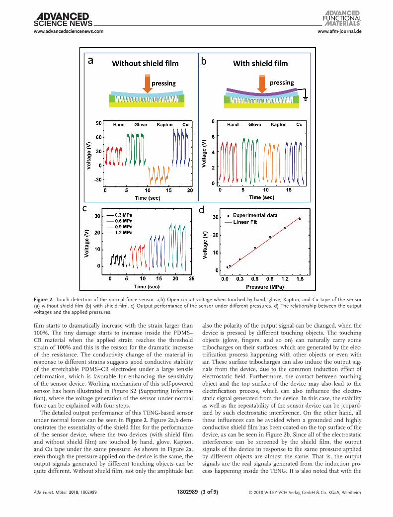
The detailed output performance of this TENG-based sensor under normal forces can be seen in Figure 2. Figure 2a,b dem-onstrates the essentiality of the shield film for the performance of the sensor device, where the two devices (with shield film and without shield film) are touched by hand, glove, Kapton, and Cu tape under the same pressure. As shown in Figure 2a, even though the pressure applied on the device is the same, the output signals generated by different touching objects can be quite different. Without shield film, not only the amplitude but
also the polarity of the output signal can be changed, when the device is pressed by different touching objects. The touching objects (glove, fingers, and so on) can naturally carry some tribocharges on their surfaces, which are generated by the elec-trification process happening with other objects or even with air. These surface tribocharges can also induce the output sig-nals from the device, due to the common induction effect of electrostatic field. Furthermore, the contact between touching object and the top surface of the device may also lead to the electrification process, which can also influence the electro-static signal generated from the device. In this case, the stability as well as the repeatability of the sensor device can be jeopard-ized by such electrostatic interference. On the other hand, all these influences can be avoided when a grounded and highly conductive shield film has been coated on the top surface of the device, as can be seen in Figure 2b. Since all of the electrostatic interference can be screened by the shield film, the output signals of the device in response to the same pressure applied by different objects are almost the same. That is, the output signals are the real signals generated from the induction pro-cess happening inside the TENG. It is also noted that with the
Adv. Funct. Mater. 2018, 1802989
Figure 2. Touch detection of the normal force sensor. a,b) Open-circuit voltage when touched by hand, glove, Kapton, and Cu tape of the sensor (a) without shield film (b) with shield film. c) Output performance of the sensor under different pressures. d) The relationship between the output voltages and the applied pressures.

www.afm-journal.dewww.advancedsciencenews.com
1802989 (4 of 9) © 2018 WILEY-VCH Verlag GmbH & Co. KGaA, Weinheim
shield film, the amplitude of output voltage from the device is decreased under the same pressure. The reason is that the contribu-tion of the tribocharges carried by touching objects to the output has been removed. In this case, the good stability and repeatability of the device can be enhanced significantly with the shield film coated on the top surface of the sensor device. The shield film also has been applied in many previous studies.[35,36]
Voltage outputs with different applied pressures have been further studied to reveal the capability of this TENG-based sensor for detecting normal forces. Figure 2c shows the dynamic output signals with different pres-sures applied on the sensor device, and the summarized changing relationship can be seen in Figure 2d. As shown in Figure 2d, the value of output voltage rises linearly with the increasing pressure, which can be used to quantitatively measure the amplitude of the pressure. The maximal sensing pressure could reach to 1.5 MPa with a sensitivity of 51.43 kPa V−1. It is necessary to point out that a brief linear behavior can be achieved in the pressure range from 0.1 to 1.5 MPa in our measurement. The result indicates that within this pressure range, the elastic deformation of the film is still in the linear region and the edge effect of the TENG is not so significant in this process. If we keep increasing the applied pressure, the elastic performance of the PDMS film will reach its compres-sion limit gradually and the linear performance of the voltage change can be influenced. When the applied pressure is larger than 1.5 MPa, the linear performance of the voltage change in response to pressure would be suppressed, as can be seen in Figure S3 (Supporting Information). Theoretically, this TENG-based sensor is a full elastic device and the compression defor-mation with different applied forces can satisfy the Hooke’s law, which means the value of output voltage increases linearly with the applied force. However, the voltage output from TENG can be influenced by many factors, such as the edge effect of TENG[37,38] and the compression limit of elastic materials. In this case, the linearity of the measurement can only be main-tained within certain pressure range.
2.2. The Self-Powered Sensor for Detecting both Normal Force and Tangential Force
Based on the above sensor for detecting normal force, we have further designed a three-axial force sensor that can detect both normal and tangential forces, the detailed structure design and photographs of which can be seen in Figure 3a,b. As is shown in Figure 3a, four stretchable PDMS–CB electrodes with tiny burr arrays are arranged neatly at the PDMS substrate with an interval between each other. The electrodes are covered by a large PDMS dielectric film with tiny burr arrays and a highly conductive shield film is coated on the top surface of the whole device. The device is packaged with four spacers at the four
corners and a single-electrode TENG with four-partitioned electrode structure is developed accordingly. The operation of this three-axial force sensor for detecting compound force (with both normal component and tangential component) can be divided into two steps. First, the normal component of the applied force leads to the compression deformation of tiny burr arrays on the contact interface and the elastic deformation of PDMS dielectric film. Accordingly, the electrical potentials of four independent electrodes are uniformly decreased, the working mechanism of which is the same as the illustration in Figure 1 and Figure S2 (Supporting Information). Then, the shear deformation of tiny burr arrays and elastic deforma-tion of the PDMS film in 2D region are induced under the tangential force, which can induce different potential changes on four electrodes. In this case, the tangential force can be detected by comparing output signals from four electrodes. The mechanism of voltage generated by elastic deformation of the PDMS film is demonstrated in Figure 3c. Here, a two-electrode case (E1 and E2) is used to illustrate this mechanism and the analysis can be extended to the four-electrode case. In the original state (Figure 3c(i)), negative charges are induced on the tiny burr area of PDMS dielectric film, while related positive charges are accumulated on the top surface of PDMS–CB electrodes. When the tensile deformation of the top dielec-tric film is induced under the tangential force, the overlapping area between tiny burr areas of PDMS film and PDMS–CB electrodes would change. In this case, the deformation would lead to the change of the amount of induced charges on the two electrodes, as can be seen in Figure 3c(ii). That is, the amount of positive charges on E1 electrode deceases and the amount on E2 electrode increases when the tangential force is applied from E1 to E2 direction (Figure 3c(iii)). Correspondingly, the output voltage from E1 electrode is increased, while the output
Adv. Funct. Mater. 2018, 1802989
Figure 3. Structural illustration of the three-axial force sensor. a) Structure design of the three-axial force sensor. b) Photographs of the three-axial force sensor. c) Detailed mechanism of the voltage generated from the elastic deformation of the dielectric film.

www.afm-journal.dewww.advancedsciencenews.com
1802989 (5 of 9) © 2018 WILEY-VCH Verlag GmbH & Co. KGaA, Weinheim
voltage from E2 is decreased. Then, when the top dielectric film returns to its original position, the charges on the electrodes also change back to its original state (Figure 3c(iV)). Since change of the charges on the electrodes is determined by the tensile deformation induce with tangential forces, the tangen-tial force can be detected and analyzed based on the different output signals from the electrodes.
Figure 4a elaborates the output performance of this three-axial force sensor under the compound force. Here, we still employ the two-electrode (E1 and E2) case to illustrate the results. The normal force (20 N) and tangential force (10 N) are successively applied on the sensor and output signals from E1 and E2 electrodes are continuously recorded. As shown in Figure 4a, the output voltages from E1 and E2 both decrease sharply when the sensor is pressed by the normal force. When the tangential force is applied from E1 to E2 direction based on above normal force, the output voltage from E1 decreases,
while the output voltage from E2 increases. In this case, both the amplitude and the direction of the applied tangential force can be analyzed by comparing the output signals from the two electrodes, which are in good agreements with the mecha-nism analysis in Figure 3c. In order to clarify the relationship between the output signal and amplitude of the tangential force, dynamic output signal from one electrode has been measured. As can be seen in Figure 4b,c, two kinds of force amplitudes (from 0 to 0.8 N and from 0 to 38 N) are, respec-tively, applied on the sensor. The change of force amplitude can be well followed by the change of output values, which suggests that the sensor can effectively measure the tangential force of different scales. It is also noted that the exerting times for different tangential forces have little difference, where longer time interval may be necessary for the case of larger tangential force. Since this sensor device is fabricated by fully elastic materials, the viscoelastic deformation of the dielectric
Adv. Funct. Mater. 2018, 1802989
Figure 4. Detection of the three-axial force sensor. a) Output performance of the three-axial force sensor under the compound force. b,c) Dynamic output signal from one electrode of the sensor in response to the two kinds of force amplitude (b) from 0 to 0.8 N (c) from 0 N to 38 N. d) The detailed relationship between the value of output voltage and the amplitude of tangential force. e,f) The stress–strain of the sensor (e) with flat interface (f) with tiny burr arrays on the contact interface, Fz = 20 N.

www.afm-journal.dewww.advancedsciencenews.com
1802989 (6 of 9) © 2018 WILEY-VCH Verlag GmbH & Co. KGaA, Weinheim
film under the force needs a certain relaxation time to achieve steady state. Furthermore, the behavior would become more significant with the increase of applied force. The fact has been carefully studied by our previous study and by many other researchers.[39–41] Hence, for the case of small tangential force in Figure 4b, the bending of the tiny burr arrays can quickly reach its saturation state. For the case of larger tangential force in Figure 4c, we need to prolong the time interval between different force values to rule out the influence of viscoelastic relaxation of PDMS dielectric film.
Meanwhile, by increasing the testing cycles, the good cor-respondence between the output voltage value and force amplitude has been demonstrated in Figure S4a,b (Supporting Information), which confirms the repeatability of the device. The detailed relationship between the value of output voltage and the amplitude of tangential force is shown in Figure 4d. Here, the change of the output voltages may have three stages with increasing tangential force. The detailed explanation related to this dynamic behavior based on deformation of tiny burr arrays and dielectric film can be seen in Figure S4c (Sup-porting Information). As is shown in Figure S4c(i) (Supporting Information), the first stage is related to the sheer deformation of tiny burr arrays. In this stage, tiny burr arrays, which origi-nally point at the vertical direction, are pressed down to one direction under the tangential force. In this case, triboelectri-fication is induced and the voltage outputs from the electrodes can be generated. The sheer deformation of tiny burr arrays requires only a small tangential force and thus the detected forces related to this stage are 0.5–3 N with rough sensitivity of 0.83 N V−1, as shown in Figure 4d(i). When the sheer deforma-tion of tiny burr arrays reaches the largest state (the tangential force >3 N), the tensile deformation of PDMS film in 2D region happens (Figure S4c(ii), Supporting Information). The elastic deformation of PDMS film leads to the second stage of the output, as can be seen in Figure 4d(ii). The change of voltage in this stage is significant, due to the change of overlapping area between tiny burr areas of PDMS film and PDMS–CB elec-trodes. Another linear relationship between the value of output voltage and increasing tangential force is obtained, while the changing slope is different from the first stage. In this stage, the value of output voltage will increase from 5 to around 19 V with rough sensitivity of 2.50 N V−1. As the tangential force reaches beyond 40 N, the change of overlapping area of tiny burr areas reaches the maximum value (Figure S4c(iii), Sup-porting Information), which results in the saturation of the output voltages from the electrodes (Figure 4d(iii)). Hence, the range of tangential force from 0.5 to 40 N can be efficiently detected by the change of output from this sensor device. The detection of static forces can also be realized by using this sensor. As is shown in Figure S4d,e (Supporting information), the step changing of the voltage is in good agreement with the applied static force. In addition, it is necessary to point out that tiny burr arrays printed on the surfaces of PDMS and PDMS–CB films are crucial to enhance the sensitivity of tangential force detection. The comparative study between the flat inter-face and the interface with tiny burr arrays has been done, as can be seen in Figure 4e,f. The lateral slide between two flat films is difficult to happen with small tangential force (<10 N), which may be resulting from the strong adherent surface
characteristic of PDMS and PDMS–CB films. In this case, the sensitivity of the device for tangential force detecting may be suppressed. However, the shearing strain is quite significant when the same tangential forces are applied on the interface with tiny burr arrays, as is shown in Figure 4f. The compared results well demonstrate the superiority of the contact inter-face with tiny burr arrays for detecting the shearing strain and tangential forces.
The direction of the applied tangential forces can also be distinguished by this three-axial force sensor. The schematic diagram and dynamic outputs of the sensor can be seen in Figure 5, where the tangential forces are applied from dif-ferent directions. The deformation directions of PDMS film are different in 2D region when tangential forces from different directions are applied, which lead to the different output signals from four electrodes (E1, E2, E3, E4). Here, the output voltage values of four electrodes are set to zero level when no tangen-tial force is applied. Therefore, the tangential force applied in “x-” or “y-”directions can be distinguished by checking the polarity of the output voltages from four electrodes, as shown in Figure 5a,b. Theoretically, the magnitude of output voltages from the same electrode should be the same, when the tan-gential force with the same magnitude is applied in “x-” and “y-”directions. However, the slight difference of the amplitude of the output from the same electrode induces, as can be seen in Figure 5a,b. There may be two reasons why the different amplitude of the output is obtained. First, the mechanical instability can cause some change during the measurement. The assembling process of this sensor is made by human hand and some position deviations may happen, which may cause the change of the elastic behavior in different directions. The second reason can be found from the detailed joint behavior of tiny burr arrays between top and bottom sides, as is shown in Figure S1c (Supporting information). During the operation, tiny burr arrays on PDMS film and PDMS–CB electrode need to inosculate with each other. However, in the real experiment, we have found that some tiny burrs can well inosculate with the related ones, while some of them are in disorder. This imperfect joint interface may result in the different sliding resistances in x-direction and y-direction. In order to confirm this fact, another measurement has been prepared (Figure S5, Supporting information). Here, the output voltage of a single PDMS–CB electrode sensor device detected with the same tangential force of 10 N from “x-”direction and “y-”direction is applied. The magnitude of output voltages in the two cases is slightly different, which is corresponding with the above analysis and measurement result in Figure 5a,b. Meanwhile, the output signals from four electrodes with the tangential force applied on 45° direction can be seen in Figure 5c. In this case, the output voltage from E4 electrode decreases, while the output voltages from all the other electrodes increase. Fur-thermore, the twisting force applied on the sensor can also be detected by the output signals, the schematic diagram of which is shown in Figure 5d. The change of overlapping area of tiny burr arrays during different twisting deformations of the PDMS film is shown in Figure 5e. Here, S0 is the orig-inal overlapping area at torsion angle of 0° when no twisting force is applied, while S is the overlapping area at different torsion angles induced by different twisting forces. Based on
Adv. Funct. Mater. 2018, 1802989

www.afm-journal.dewww.advancedsciencenews.com
1802989 (7 of 9) © 2018 WILEY-VCH Verlag GmbH & Co. KGaA, Weinheim
the geometric analysis, the overlapping area would reach the minimum value at the torsion angle of 45° and then increases to the original value at 90°. For our sensor device, since the top PDMS dielectric film and the bottom four electrodes are packaged together, the twisting deformation of PDMS film has a maximum torsion angle smaller than 25°. Therefore, the overlapping area of tiny burr arrays between PDMS film and each PDMS–CB electrode is always decreasing within this twisting range. The interface between PDMS film and PDMS–CB electrodes can provide a notable resisting force to impede the twisting deformation of PDMS film. With the increase of the rotation angle, the resisting force that is generated by the tiny burr arrays on tribointerface will increase constantly, which can establish a relationship between the rotation angle and the required twisting force. The dynamic outputs from four electrodes with the applied twisting forces can be seen in Figure 5f,g, where the corresponding static torque is 0.056 and 0.14 N m, respectively.
Applicability of the sensor for tactile sensing and mechan-ical vibration detection is demonstrated experimentally. As shown in Figure 6a, a mini tangential force sensor with only two PDMS–CB electrodes is fabricated. Two rectangular elec-trodes are arranged neatly with an interval of 3 mm at the bottom PDMS substrate (see the inset in Figure 6a and the size of the device is around 1 cm2). The real-time output signals of this mini sensor in response to finger touching can be seen in Figure 6b and Figure S6a (Supporting Information). The output voltages from two electrodes are measured simultaneously by two computers and the dynamic detecting process can be seen in Movie S1 (Supporting Information). The amplitude and the direction of the tangential force applied by finger can be dis-tinguished based on the output signals from two electrodes. In this case, this small device may be potentially applied for wear-able electronic devices and human–machine interaction. Mean-while, the potential application of the three-axial force sensor for detecting 1D mechanical vibration is also demonstrated.
Adv. Funct. Mater. 2018, 1802989
Figure 5. Detection of tangential forces applied from different direction. a–c) Schematic diagram and dynamic outputs of the three-axial force sensor with the tangential force applied along (a) x-axis, (b) y-axis, (c) 45° angle direction. d) Schematic of the twisting deformation of PDMS film under twisting force. e) The change of overlapping area of tiny burr arrays between PDMS film and PDMS–CB electrodes with different twisting deformations. f,g) Dynamic output signals from four electrodes under the twisting forces, where the corresponding static torque is (f) 0.056 N m and (g) 0.14 N m.

www.afm-journal.dewww.advancedsciencenews.com
1802989 (8 of 9) © 2018 WILEY-VCH Verlag GmbH & Co. KGaA, Weinheim
Figure 6c shows the platform and system for mechanical vibration detection, where the inset is the photograph of the modified sensor for detecting vibration. Two acrylic plates are placed on the top and bottom surfaces of the sensor so that it can slide freely in a single direction, while push–pull motion cycles are applied on the sensor device for triggering 1D vibra-tion. The output signals of this modified sensor generated from the vibrations can be seen in Figure 6d. Furthermore, a mass block of 200 g is placed on the top acrylic plate to increase the load of the device in vertical direction. Then, the same vibra-tion motion is detected by this sensor and the output signal of the sensor is shown in Figure S6c and Movie S2 (Supporting Information). The output voltage of the sensor is increased with the mass block under the same vibration. This is due to the increase of sliding distance of PDMS film during vibration motions, which is caused by the stronger inertial reaction with the mass block. Since the output signals of the three-axial force sensor can be generated by mechanical vibration, the sensor is also expected to be applied in vibration monitoring system and other industrial fields.
3. Conclusion
In summary, based on the TENG in single electrode mode, we have demonstrated a simply fabricated, fully elastic, and metal-free tactile sensor for detecting both normal and tan-gential forces. The detected normal pressure could reach to 1.5 MPa with a sensitivity of about 51.43 kPa V−1. Meanwhile, the elastic deformation of the device under the action of forces
is facilitated by the tiny burr arrays on the contact interface, which enhances the sen-sitivity of this TENG-based sensor. Thus, a large range of tangential forces (0.5–40 N) can be detected by the sensor with rough sensitivity of 0.83 N V−1 (0.5–3 N) and 2.50 N V−1 (3–40 N). Moreover, with the help of the four-partitioned electrodes structure, the tangential force applied from different directions can be distinguished, and even the twisting force can also be identified based on this structure. Moreover, a grounded shield film has been coated on the top surface of the device and thus the stability and repeat-ability of the sensor can be significantly enhanced. Considering these characteristics, the proposed tactile sensor is expected to be applied in fields such as industrial robotics, wearable electronics, and human–machine interactions.
4. Experimental SectionPreparation of Dielectric and Electrode Film: A
PMMA plate (6 × 6 cm, thickness of 5 mm) with the matrix of tiny burr hollows was manufactured as the mold to make the film with tiny burr arrays. The matrix of tiny burr hollows was 3.2 × 3.2 cm at the center of PMMA plate, while the diameter of tiny
burr hollow was about 500 µm and the depth was around 1.8 mm. Tiny burr hollows were sculptured by engraving machine laser (UNIVERSAL PLS6.75, USA) and the parameters of engraving machine laser were as follows: the working mode was V-D, the pixels per inch was 1000, while the sculptured depth was no more than 2 mm with the power of 40% and the velocity of 3%. Then, PDMS (Dow Corning, Sylgard 184; ratio of base to cross-linker, 10:1 by mass) was poured into the mold and coated with a spin rod. After that, it was vacuumed for 1 h and cured at 90 °C for 1.5 h. Then, the PDMS film with cured tiny burrs structure was peeled off slowly with a tweezer. For PDMS–CB electrode film, the curing liquid was made by mixing PDMS and carbon black (TIMICAL SUPER P LI). The mass ratio of PDMS and carbon black was 10:0.7. The mixed curing liquid would be cast and molded with the same condition of PDMS film.
Fabrication of Normal Force Detecting Sensor: The PDMS film of 6 × 6 cm and PDMS–CB electrode layer of 6 × 6 cm were assembled face to face. Then, a spacer (height = 4 mm) was placed between two layers to increase the detached distance of them, the materials of which could be PMMA or PDMS. After that, a shield film with dimension of 6 × 6 cm and thickness about 150 µm was coated on the top surface of the device. The material of the shield film was also PDMS–CB, while the mass ratio of PDMS and carbon black was 10:1.5 there, with a maximum resistance less than 300 Ω.
Fabrication of Three-Axial Force Sensor: Four PDMS–CB electrodes of 1.8 × 1.8 cm were positioned on the PDMS substrate (6 × 6 cm, thickness = 1 mm) with four spacers (height = 4 mm) at the four corners, where the electrodes were bonded in position with liquid PDMS. Then, they were cured at 50 °C for 1 h to unite as one. After that, the combined four positive electrodes and the PDMS dielectric film with tiny burr arrays were assembled face to face. The shield film connected to ground was coated on the top surface of PDMS film, and the sensor was packaged before it was experimented and tested.
Characterization: For tangential characterizations, a preload normal force of 20 N was always applied. The tangential force load–unload cycles were controlled by a numerical control linear motor and the
Adv. Funct. Mater. 2018, 1802989
Figure 6. Applicability of three-axial force sensor for tactile sensing and mechanical vibration detection. a) Photograph of the mini two-electrode tangential force sensor. b) Screenshot of the real-time output signals of the mini sensor for finger touch detection. c) Platform and system for mechanical vibration detection. d) Output signals of the modified three-axial force sensor for vibration detection.

www.afm-journal.dewww.advancedsciencenews.com
1802989 (9 of 9) © 2018 WILEY-VCH Verlag GmbH & Co. KGaA, Weinheim
real-time output signals were monitored by load cell and digital-display dynamometer connected to computers. To measure the shear strain accurately, the sensor was fixed on the micropositioning platform and a circular strain test was carried out. During actuation, video images of the biaxial extension of the electrode area were captured using camera (Canon 600D, Japan) and high-speed camera (Photron, Japan), while the captured video and images were analyzed using Premiere and Adobe Photoshop software. The outputs of the sensor in response to forces were measured by Stanford Research Systems Keithley 6514.
Supporting InformationSupporting Information is available from the Wiley Online Library or from the author.
AcknowledgementsThis work was supported by the National Key R & D Project from Minister of Science and Technology (2016YFA0202704), the Beijing Municipal Science & Technology Commission (Z171100000317001), the “thousands talents” program for pioneer researcher and his innovation team, China, the NSFC Key Program (No. 21237003), and the National Natural Science Foundation of China (Grant Nos. 51775049, 51432005, 11674215, 5151101243, 51561145021).
Conflict of InterestThe authors declare no conflict of interest.
Keywordsnormal forces, tactile sensors, tangential forces, triboelectric nanogenerators
Received: May 1, 2018Published online:
[1] K. Parida, V. Kumar, W. Jiangxin, V. Bhavanasi, R. Bendi, P. S. Lee, Adv. Mater. 2017, 29, 1702181.
[2] T. Q. Trung, N. E. Lee, Adv. Mater. 2016, 28, 4338.[3] C. C. Kim, H. H. Lee, K. H. Oh, J. Y. Sun, Science 2016, 353, 682.[4] Y. Wan, Y. Wang, C. F. Guo, Mater. Today Phys. 2017, 1, 61.[5] B. Wang, C. Liu, Y. Xiao, J. Zhong, W. Li, Y. Cheng, B. Hu, L. Huang,
J. Zhou, Nano Energy 2017, 32, 42.[6] L. W. Yap, S. Gong, Y. Tang, Y. Zhu, W. Cheng, Sci. Bull. 2016, 61,
1624.[7] X. Chen, Y. Wu, J. Shao, T. Jiang, A. Yu, L. Xu, Z. L. Wang, Small
2017, 13, 1702929.[8] K. Sangwoo, C. Seongdae, O. Eunho, B. Junghwan, K. Hyunjong,
L. Byeongmoon, L. Seunghwan, Y. Hong, Sci. Rep. 2016, 6, 34632.[9] B. Hu, W. Chen, J. Zhou, Sens. Actuators, B 2013, 176, 522.
[10] S. Gong, W. Schwalb, Y. Wang, Y. Chen, Y. Tang, J. Si, B. Shirinzadeh, W. Cheng, Nat. Commun. 2014, 5, 3132.
[11] R. Surapaneni, Q. Guo, Y. Xie, D. J. Young, C. H. Mastrangelo, J. Micromech. Microeng. 2013, 23, 075004.
[12] H. Takahashi, A. Nakai, N. Thanh-Vinh, K. Matsumoto, I. Shimoyama, Sens. Actuators, A 2013, 199, 43.
[13] G. Zhang, Q. Liao, M. Ma, Z. Zhang, H. Si, S. Liu, X. Zheng, Y. Ding, Y. Zhang, Nano Energy 2016, 30, 180.
[14] S. H. Liu, L. F. Wang, X. L. Feng, Z. Wang, Q. Xu, S. Bai, Y. Qin, Z. L. Wang, Adv. Mater. 2017, 29, 1606346.
[15] S. Wang, L. Lin, Z. L. Wang, Nano Energy 2015, 11, 436.[16] X. Chen, M. Iwamoto, Z. Shi, L. Zhang, Z. L. Wang,
Adv. Funct. Mater. 2015, 25, 739.[17] Y. Cheng, C. Wang, J. Zhong, S. Lin, Y. Xiao, Q. Zhong, H. Jiang,
N. Wu, W. Li, S. Chen, Nano Energy 2017, 34, 562.[18] Q. Liang, Z. Zheng, X. Yan, Y. Gu, Y. Zhao, G. Zhang, S. Lu, Q. Liao,
Y. Zhang, Nano Energy 2015, 14, 209.[19] X. Chen, T. Jiang, Y. Yao, L. Xu, Z. Zhao, Z. L. Wang,
Adv. Funct. Mater. 2016, 26, 4906.[20] Q. Liang, Q. Zhang, X. Yan, X. Liao, L. Han, F. Yi, M. Ma, Y. Zhang,
Adv. Mater. 2017, 29, 1604961.[21] Q. Liang, X. Yan, Y. Gu, K. Zhang, M. Liang, S. Lu, X. Zheng,
Y. Zhang, Sci. Rep. 2015, 5, 9080.[22] X. Chen, X. Pu, T. Jiang, A. Yu, L. Xu, Z. L. Wang, Adv. Funct. Mater.
2016, 27, 1603788.[23] A. Yu, X. Chen, R. Wang, J. Liu, J. Luo, L. Chen, Y. Zhang, W. Wu,
C. Liu, H. Yuan, ACS Nano 2016, 10, 3944.[24] X. Chen, Y. Wu, A. Yu, L. Xu, L. Zheng, Y. Liu, H. Li, Z. L. Wang,
Nano Energy 2017, 38, 91.[25] L. Zheng, Y. Wu, X. Chen, A. Yu, L. Xu, Y. Liu, H. Li, Z. L. Wang,
Adv. Funct. Mater. 2017, 27, 1606408.[26] K. Liu, T. Ding, X. Mo, Q. Chen, P. Yang, J. Li, W. Xie, Y. Zhou,
J. Zhou, Nano Energy 2016, 30, 684.[27] J. Nie, Z. Ren, J. Shao, C. Deng, L. Xu, X. Chen, M. Li, Z. L. Wang,
ACS Nano 2018, 12, 1491.[28] L. Viry, A. Levi, M. Totaro, A. Mondini, V. Mattoli, B. Mazzolai,
L. Beccai, Adv. Mater. 2014, 26, 2659.[29] M. Ma, Z. Zhang, Q. Liao, F. Yi, L. Han, G. Zhang, S. Liu, X. Liao,
Y. Zhang, Nano Energy 2017, 32, 389.[30] V. Maheshwari, R. F. Saraf, Science 2006, 312, 1501.[31] M. F. Lin, J. Xiong, J. Wang, K. Parida, P. S. Lee, Nano Energy 2018,
44, 248.[32] L. Wang, J. A. Jackman, E. L. Tan, J. H. Park, M. G. Potroz,
E. T. Hwang, N. J. Cho, Nano Energy 2017, 36, 38.[33] X. Wang, J. Hao, Sci. Bull. 2016, 61, 1281.[34] Y. L. Xu, X. H. Zhang, S. Zhu, S. Zhan, Sci. Bull. 2016, 61,
313.[35] S. Li, W. Peng, J. Wang, L. Lin, Y. Zi, G. Zhang, Z. L. Wang, ACS
Nano 2016, 10, 7973.[36] C. Wu, W. Ding, R. Liu, J. Wang, A. C. Wang, J. Wang, S. Li, Y. Zi,
Z. L. Wang, Mater. Today 2018, 21, 216.[37] S. Niu, Y. Liu, S. Wang, L. Lin, Y. Zhou, Y. Han, Z. L. Wang,
Adv. Funct. Mater. 2014, 24, 3332.[38] S. Niu, Z. L. Wang, Nano Energy 2015, 14, 161.[39] X. Chen, T. Jiang, Z. L. Wang, Appl. Phys. Lett. 2017, 110, 033505.[40] C. C. Foo, S. Cai, S. Koh, S. Bauer, Z. Suo, J. Appl. Phys. 2012, 111,
034102.[41] J. Huang, T. Li, C. Chiang Foo, J. Zhu, D. R. Clarke, Z. Suo,
Appl. Phys. Lett. 2012, 100, 041911.
Adv. Funct. Mater. 2018, 1802989