Embed Size (px)
Citation preview
Fully Integrated CMOS Phased-array PLL
Transmitters
by
Li Li
A dissertation submitted in partial fulfillment
of the requirements for the degree of
Doctor of Philosophy
(Electrical Engineering)
in The University of Michigan
2012
Doctoral Committee:
Associate Professor Michael Flynn, Chair
Professor Amir Mortazawi
Associate Professor Jerome P. Lynch
Assistant Professor Zhengya Zhang
© Li Li
2012
ii
ACKNOWLEDGMENTS
Thanks everyone!
Firstly, I would like to thank my advisor, Professor Michael Flynn. It’s been a
long and tough journey for the past six years. Professor Flynn provided the financial
support and technical advice for me to get through this Ph.D. program. I would also
like to thank the rest of my committee members: Professor Jerome P. Lynch,
Professor Amir Mortazawi and Professor Zhengya Zhang. Their help and advice were
always helpful.
I’d like to thank all of my past and present group members. I could never have
gotten here without your technical advice, inspiration, and most importantly mental
support to keep me sane enough to get through the six memorable Michigan winters.
In no particular orders these include David Lin, Joshua Kang, Junyoung Park, Mark
Ferriss, Ivan Bogue, Chun Chieh Lee, Jongwoo Lee, Shahrzad Naraghi, Dan Shi, Ben
Rhew, Hyungil Chae, Nick Collins, Jeff Fredenburg, Mohammad Ghahramani, Jorge
Pernillo, Jaehun Jeong, Aaron Rocca, Andres Tamez, and Chunyang Zhai.
I’d also like to thank SRC, WIMS, and MAST for funding my Ph.D. program.
This work would not have been possible without their generous support.
And finally I’d like to thank my mom for everything.
iii
Table of Contents
Acknowledgents ............................................................................................................. ii
List of Figures ........................................................................................................................... v
ABSTRACT .............................................................................................................................. viii
Chapter 1 Introduction .......................................................................................................... 1
1.1. Background .............................................................................................................. 1
1.2. Introduction to Phased Array ................................................................................ 4
1.2.1. Phased array theory ........................................................................................ 5
1.3. Existing Phased Array Architectures ..................................................................... 9
1.3.1. Phase shift at RF .............................................................................................. 9
1.3.2. Phase shift at DC/IF ......................................................................................... 9
1.3.3. Phase shift at LO ............................................................................................ 11
1.3.4. Summary of the architectures ..................................................................... 12
1.4. Existing phase shifter ............................................................................................ 13
1.4.1. Lumped element phase shifter .................................................................... 13
1.4.2. Multiphase VCO ............................................................................................. 14
1.4.3. Active phase interpolation ........................................................................... 15
1.5. Conclusion .............................................................................................................. 18
Chapter 2 PLL Basics ............................................................................................................. 19
2.1. Introduction to PLL ................................................................................................ 19
2.2. Traditional charge-pump phase detector .......................................................... 22
2.3. Type I PLL vs. Type II PLL ....................................................................................... 24
2.4. Fractional-N divider ............................................................................................... 26
2.5. PLL phase noise analysis ....................................................................................... 28
Chapter 3 Phase-Setting PLL ................................................................................................ 30
3.1. Background ............................................................................................................ 30
iv
3.2. Overview of phase control mechanism .............................................................. 31
3.3. PLL architecture ..................................................................................................... 33
3.3.1. 1-bit TDC PFD ................................................................................................. 34
3.3.2. PLL Type .......................................................................................................... 36
3.3.3. Loop filter ....................................................................................................... 37
3.3.4. VCO .................................................................................................................. 41
3.4. Data modulation .................................................................................................... 43
3.4.1. Divide ratio modulation ................................................................................ 43
3.4.2. Direct phase modulation .............................................................................. 45
3.5. Phased array and conclusion ............................................................................... 46
Chapter 4 Prototypes and Measurements ........................................................................ 48
4.1. Overview ................................................................................................................. 48
4.2. First Prototype ....................................................................................................... 49
4.3. Second Prototype .................................................................................................. 51
4.4. Third Prototype ...................................................................................................... 55
Chapter 5 Conclusion ............................................................................................................ 61
5.1. Key contributions .................................................................................................. 61
5.2. Future works .......................................................................................................... 63
Appendix A A flexible wireless receiver with configurable DT filter embedded
in a SAR ADC ........................................................................................................................... 66
A.1 Introduction ................................................................................................... 66
A.2 Receiver Architecture ................................................................................... 67
A.3 SAR ADC with Embedded DT filter .............................................................. 69
A.4 Results ............................................................................................................. 71
Reference ............................................................................................................................... 72
v
List of Figures
Figure 1: Phased array transmitter ............................................................................... 4
Figure 2: 1-D linear phased array .................................................................................. 5
Figure 3: Array factor as a function of delay time ωτ in 45o steps ............................... 7
Figure 4: Array factor vs radiation angle in polar coordinates (a) -30o (b) -15o (c) 0o (d)
15o ................................................................................................................................. 8
Figure 5: Transmitter with phase shift at RF ............................................................... 10
Figure 6: Transmitter with phase shift at DC .............................................................. 10
Figure 7: Transmitter with phase shift at LO .............................................................. 11
Figure 8: Comparison of the three phased array architectures ................................. 12
Figure 9: Varactor-loaded transmission line phase shifter ......................................... 14
Figure 10: Schematic of a 16 phase ring VCO ............................................................. 14
Figure 11: Phase interpolation scheme ...................................................................... 16
Figure 12: Phase rotator schematic ............................................................................ 17
Figure 13: Simple PLL block diagram .......................................................................... 20
Figure 14: Linear PLL model ........................................................................................ 20
Figure 15: Charge-pump PLL schematic ...................................................................... 22
Figure 16: Simplified charge pump loop filter ............................................................ 24
Figure 17: First order ΣΔ modulator and typical output with a constant input ......... 27
vi
Figure 18: ΣΔ fractional-N PLL ..................................................................................... 27
Figure 19: Typical type II ΣΔ PLL phase noise plot with PLL bandwidth of 100 KHz
generated with cppsim ............................................................................................... 29
Figure 20: Two conceptual approaches to phase shift ............................................... 32
Figure 21: PLL modulator architecture ....................................................................... 34
Figure 22: 1-bit TDC PFD block diagram ..................................................................... 35
Figure 23: Linearized model of the PFD feedback loop .............................................. 37
Figure 24: Digital and analog signal domains ............................................................. 38
Figure 25: VCO and output buffer schematics ............................................................ 42
Figure 26: Divide ratio modulator ............................................................................... 43
Figure 27: two-stage cascading PLL architecture ....................................................... 44
Figure 28: Phase modulation and phase setting superimposed together ................. 45
Figure 29: Phased array system diagram .................................................................... 47
Figure 30: Die micrograph of the first prototype ....................................................... 49
Figure 31: 2MHz BFSK modulated spectrum .............................................................. 50
Figure 32: Second Prototype Die micrograph............................................................. 51
Figure 33: Locked PLL spectrum ................................................................................. 52
Figure 34: Comparison of measured type I & II mode phase noise with the same loop
parameters. ................................................................................................................. 52
Figure 35: Measured phase shift vs. input code at 5.8GHz ........................................ 53
Figure 36: Measured 34kHz QPSK constellation plot ................................................. 54
Figure 37: Third Prototype Die Micrograph ................................................................ 55
vii
Figure 38: Phase noise plot of the type II PLL ............................................................. 56
Figure 39: (a) Type II PLL spectrum and zoomed in 1MHz spectrum (b) Type I PLL
spectrum and zoomed in 1MHz spectrum with the same loop parameters as the type
II in (a) ......................................................................................................................... 56
Figure 40: Phase shift vs. digital input ........................................................................ 57
Figure 41: Phase shift test setup ................................................................................. 57
Figure 42: Measured Constellation plot of 30 kHz 8-nary PSK ................................... 58
Figure 43 Phased array PCB with 2 channels connected ............................................ 59
Figure 44: Results summary and comparison with other work .................................. 60
Figure 45: New PLL phased array architecture ........................................................... 64
Figure 46: Block diagram of the SARfilter ADC receiver ............................................. 67
Figure 47: Simplified diagram of the LNA, mixer, and transimpedance amplifier with
binary-weighed current DACs for DC offset correction .............................................. 69
Figure 48: Principle of filtering with charge sharing sampling ................................... 70
Figure 49: Timing diagram of embedded FIR filter and SAR ADC operation .............. 71
Figure 50: Die photo of the SAR filter prototype ........................................................ 71
viii
ABSTRACT
With more advanced technology, complete phased array system can be
integrated in CMOS. Integrated CMOS phased array systems offer lower cost, lower
power consumption, higher reliability and the possibility of on-chip signal processing
using ever cheaper digital circuitry. This opens up possibilities for new applications
such as directional point-to-point wireless communication which provides high
security and is less prone to jamming by interferers.
Integrated phased array systems are for the most part not too different from
normal single channel transceivers. The key additional component is the phase
shifter. A new phased array architecture that uses digital phase locked loop PLL
modulator to realize phase shift is developed. To achieve phase shifting capability,
PLL is a natural candidate. If we combine PLL’s phase shifting and modulation
capabilities then we can realize phased array system using solely PLLs. With recent
breakthrough in digital PLL, a digital PLL can generate a precise and well-controlled
phase shift that analog PLLs cannot. The same phase shift capabilities can be used for
data modulation. With both phase shift and data modulation capabilities, we only
need an array of such PLLs to realize a phased array. Compared with conventional
phased arrays, PLL based phased array can achieve more precise phase shift thus
ix
more precise radiation angle. It is also more flexible, since all channels can generate
independent phase shift.
A fully-integrated 5.8GHz PLL modulator prototype implemented in 65nm
CMOS that achieves digitally-controlled arbitrary phase generation is presented. The
PLL is a Type II fractional-N PLL with a 1-bit TDC as its PFD. Digital phase setting,
which operates by adding a proportional signal to the PFD output, is incorporated in
the PLL. The prototype achieves an average measured phase resolution of 2.25o and
phase range of more than 720o. The entire PLL and output buffer consumes 11mW.
Four of such PLLs form a prototype phased array as a proof of concept.
1
Chapter 1
Introduction
1.1. Background
Moore prophesied in his 1965 paper [1]: “The successful realization of such
items as phased-array antennas, for example, using a multiplicity of integrated
microwave power sources, could completely revolutionize radar.” Indeed, that day
has come. With more advanced technology, complete phased array system can be
integrated in CMOS. Integrated CMOS phased array systems offer lower cost, lower
power consumption, higher reliability and possibility of on-chip signal processing
using ever cheaper digital circuitry. It opens up possibilities for new applications such
as automotive radar systems. However, the application of integrated phased array
system is not limited to radar as Moore envisioned. Phased arrays can also be utilized
for directional point-to-point wireless communication, which provides high security
and is less prone to jamming by interferers. At high frequency, phased array systems
potentially offer more bandwidth, and reduce the required antenna size and spacing.
2
Integrated phased array systems are for the most part not too different from
normal single channel transceivers. The key additional component is the phase
shifter. A new phased array architecture that uses digital phase locked loop (PLL)
modulator to realize phase shift is developed. To achieve phase shifting capability,
PLL is a natural candidate. Furthermore, PLL transmitter has been extensively
studied [2][3][4]. If we combine a PLL’s phase shifting and modulation capabilities
then we can realize phased array system using solely PLLs. A digital PLL can
generate a precise and well-controlled phase shift that analog PLL cannot. With
recent developments in digital PLL architectures [5][6], digitally dominant PLL based
phased array systems are logically the next step.
This thesis focuses on PLL based phased array modulator. A digital PLL can
generate precise and well-controlled phase shift. The same phase shift capabilities can
be used for data modulation. With both phase shift and data modulation capabilities,
we only need an array of such PLLs to realize a phased array. Compared with
conventional phased arrays, PLL based phased array can achieve a more precise
phase shift thus more precise radiation angle. PLL phased array is also more flexible,
since all channels can generate independent phase shifts and produce independent
modulation. This allows the phase array to produce a single beam or multiple beams
each carrying different signals. Moreover it takes out the complicated signal routing
tree required in a conventional phased array for phase delay matching.
Furthermore accurate phase control of high-speed signals is also required in
serial links, clock distribution and medical imaging systems. A precise high
frequency phase-setting PLL can be utilized in these applications as well.
3
For example, system-on-chip (SoC) design depends greatly on reusing
semiconductor intellectual property (IP) [7]. However integrating existing IP cores
into a single synchronous SoC faces the problem of clock distribution, because of
different clock delay requirements. A clock generator with precise phase-setting
ability can be used to solve the problem and alleviate the problems of clock
distribution in large chips.
In an on-chip serial link, data is transmitted across the chip with a lossy on-
chip transmission-line [8]. When data is received and sampled at the receiver end, it is
delayed over the long transmission-line; therefore a phase shifter is needed to tune the
sampling phase for proper recovery. With a precise phase-setting PLL, we can
accurately adjust the sampling.
4
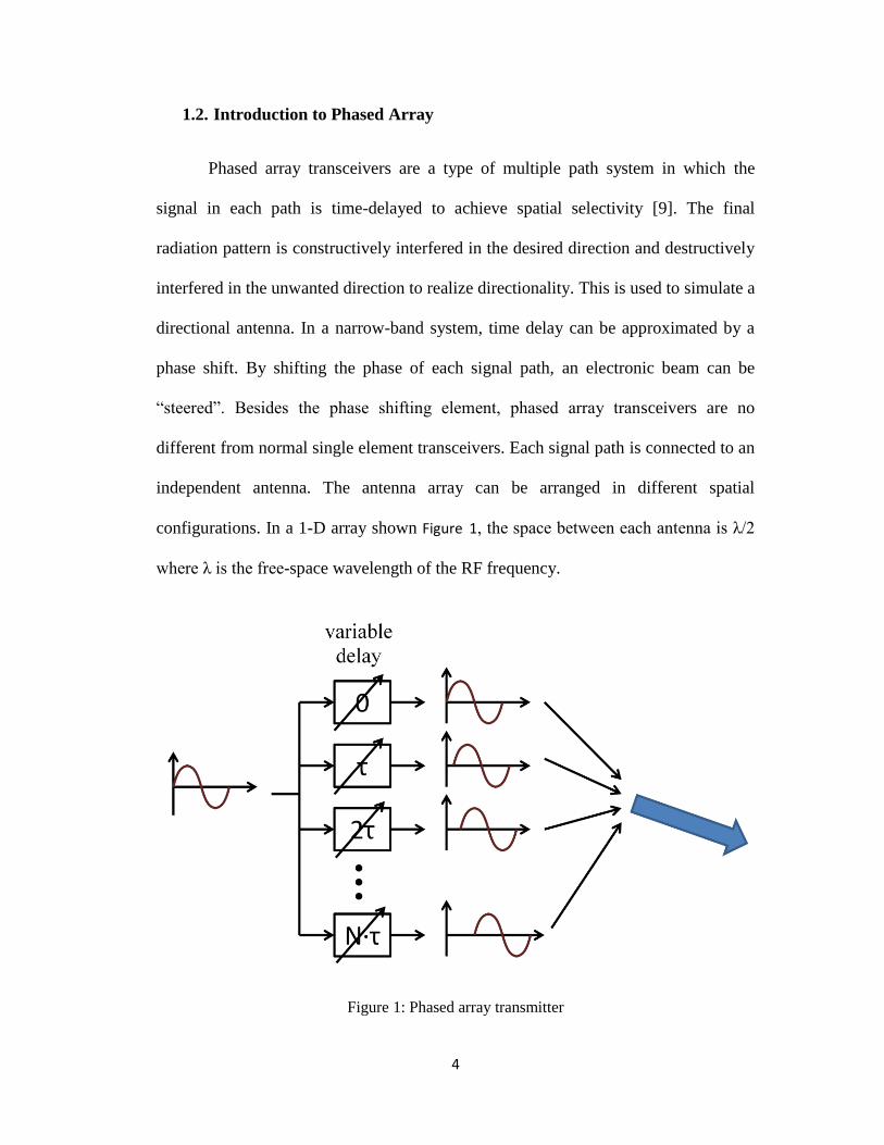
1.2. Introduction to Phased Array
Phased array transceivers are a type of multiple path system in which the
signal in each path is time-delayed to achieve spatial selectivity [9]. The final
radiation pattern is constructively interfered in the desired direction and destructively
interfered in the unwanted direction to realize directionality. This is used to simulate a
directional antenna. In a narrow-band system, time delay can be approximated by a
phase shift. By shifting the phase of each signal path, an electronic beam can be
“steered”. Besides the phase shifting element, phased array transceivers are no
different from normal single element transceivers. Each signal path is connected to an
independent antenna. The antenna array can be arranged in different spatial
configurations. In a 1-D array shown Figure 1, the space between each antenna is λ/2
where λ is the free-space wavelength of the RF frequency.
Figure 1: Phased array transmitter
5
Phased array receiver has the benefit of receiving less interferer as long as it
does not originates from the same direction as the wanted signal. For a same given
power received at the receiver, phased array transmitter requires less power than a
single element transmitter. The power radiated by an N-element phased array
transmitter is N2 times that of a single element in the desired direction, because of
constructive interference in that direction. Furthermore, lowered power requirement
in individual elements gives more design flexibilities and room for better
optimization.
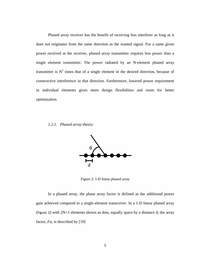
1.2.1. Phased array theory
Figure 2: 1-D linear phased array
In a phased array, the phase array factor is defined as the additional power
gain achieved compared to a single-element transceiver. In a 1-D linear phased array
(Figure 2) with 2N+1 elements shown as dots, equally space by a distance d, the array
factor, Fa, is described by [10]
6
1
where θ is the angle from origin to a point in space, In is the power of individual
element and I0 is the nominal power of a single-element transceiver. k=2π/λ and λ is
the wavelength. We need to note that distance d should be less than half wavelength
λ/2. When all elements produce the same power and same phase shift, the max power
and array factor is achieved at 90o. However if all elements have equal amplitude but
uniform progressive phase shift ωτ
2
the array factor becomes
3
Comparing equation 3 above to equation 1, we see that the peak power angle θo can
be changed from 0 in equation 1, to
4
5
Thus describes the relationship between the phase shift ωτ in individual elements and
final output radiation angle θo. Since we can only control phase shift ωτ in the
transmitter, the above equation is useful to determine the final radiation angle θo. The
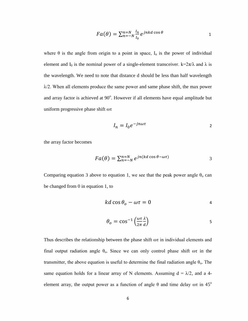
same equation holds for a linear array of N elements. Assuming d = λ/2, and a 4-
element array, the output power as a function of angle θ and time delay ωτ in 45o
7
steps is shown in Figure 3. We can also see from the figure that the peak power angle
has changed by about 14.5o for every 45
o of shift in input phase. The same 4-element
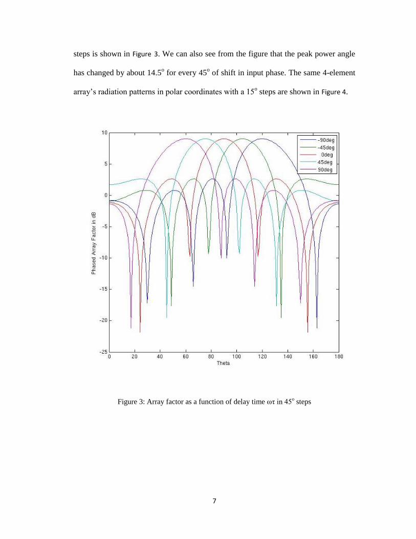
array’s radiation patterns in polar coordinates with a 15o steps are shown in Figure 4.
Figure 3: Array factor as a function of delay time ωτ in 45o steps
8
Figure 4: Array factor vs radiation angle in polar coordinates (a) -30o (b) -15
o (c) 0
o (d) 15
o
9
1.3. Existing Phased Array Architectures
As discussed earlier, phased array transceivers are no different from normal
transceivers except for the phase shift; therefore where we introduce the phase shift
gives rise to several different phase array architectures. We will only discuss the
transmitter portion, but the receiver path is more or less the same except reversed.
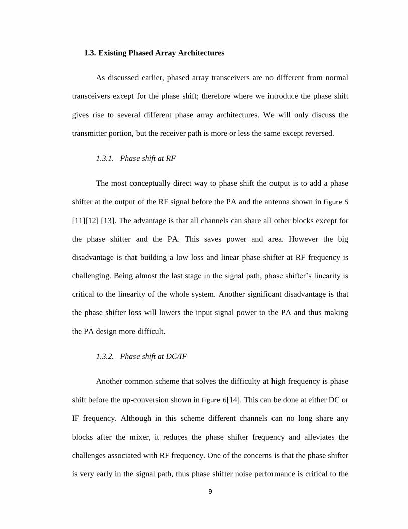
1.3.1. Phase shift at RF
The most conceptually direct way to phase shift the output is to add a phase
shifter at the output of the RF signal before the PA and the antenna shown in Figure 5
[11][12] [13]. The advantage is that all channels can share all other blocks except for
the phase shifter and the PA. This saves power and area. However the big
disadvantage is that building a low loss and linear phase shifter at RF frequency is
challenging. Being almost the last stage in the signal path, phase shifter’s linearity is
critical to the linearity of the whole system. Another significant disadvantage is that
the phase shifter loss will lowers the input signal power to the PA and thus making
the PA design more difficult.
1.3.2. Phase shift at DC/IF
Another common scheme that solves the difficulty at high frequency is phase
shift before the up-conversion shown in Figure 6[14]. This can be done at either DC or
IF frequency. Although in this scheme different channels can no long share any
blocks after the mixer, it reduces the phase shifter frequency and alleviates the
challenges associated with RF frequency. One of the concerns is that the phase shifter
is very early in the signal path, thus phase shifter noise performance is critical to the
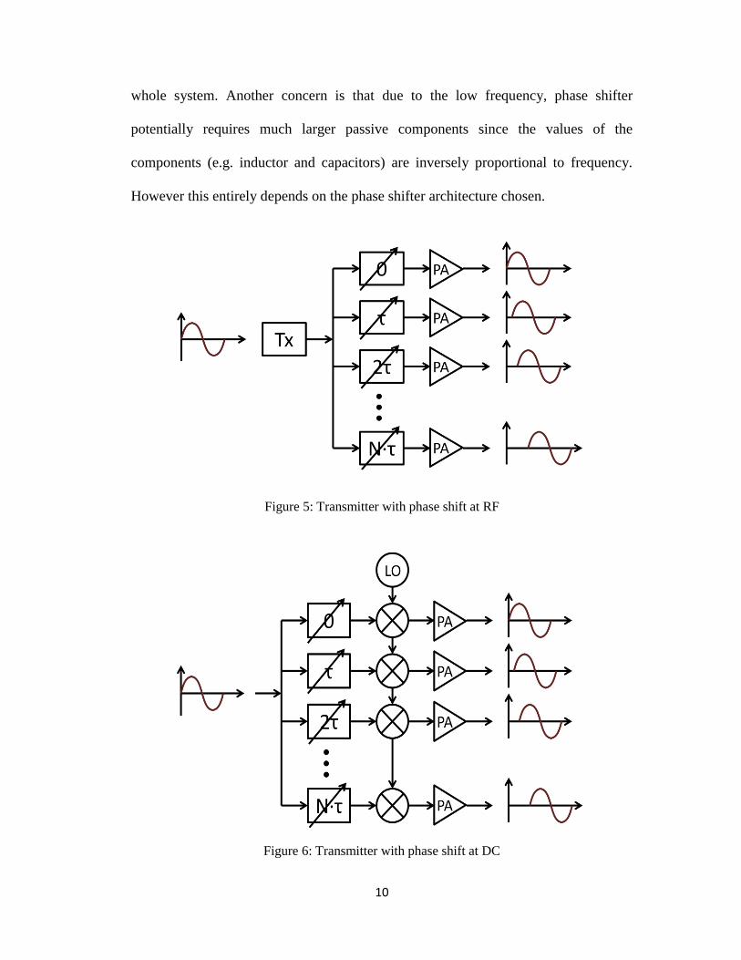
10
whole system. Another concern is that due to the low frequency, phase shifter
potentially requires much larger passive components since the values of the
components (e.g. inductor and capacitors) are inversely proportional to frequency.
However this entirely depends on the phase shifter architecture chosen.
Figure 5: Transmitter with phase shift at RF
Figure 6: Transmitter with phase shift at DC
11
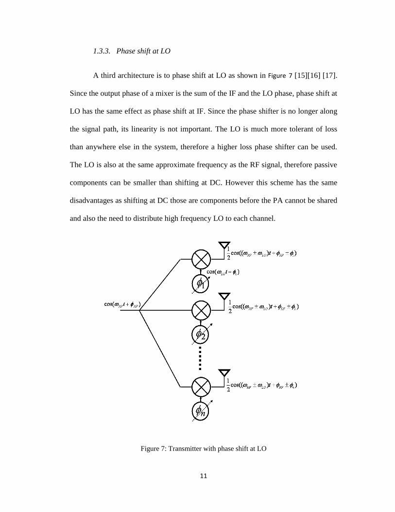
1.3.3. Phase shift at LO
A third architecture is to phase shift at LO as shown in Figure 7 [15][16] [17].
Since the output phase of a mixer is the sum of the IF and the LO phase, phase shift at
LO has the same effect as phase shift at IF. Since the phase shifter is no longer along
the signal path, its linearity is not important. The LO is much more tolerant of loss
than anywhere else in the system, therefore a higher loss phase shifter can be used.
The LO is also at the same approximate frequency as the RF signal, therefore passive
components can be smaller than shifting at DC. However this scheme has the same
disadvantages as shifting at DC those are components before the PA cannot be shared
and also the need to distribute high frequency LO to each channel.
Figure 7: Transmitter with phase shift at LO
12
1.3.4. Summary of the architectures
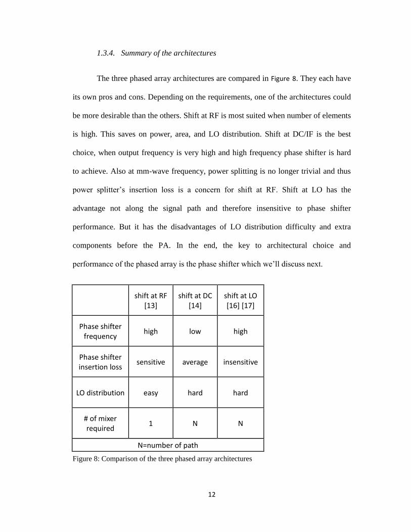
The three phased array architectures are compared in Figure 8. They each have
its own pros and cons. Depending on the requirements, one of the architectures could
be more desirable than the others. Shift at RF is most suited when number of elements
is high. This saves on power, area, and LO distribution. Shift at DC/IF is the best
choice, when output frequency is very high and high frequency phase shifter is hard
to achieve. Also at mm-wave frequency, power splitting is no longer trivial and thus
power splitter’s insertion loss is a concern for shift at RF. Shift at LO has the
advantage not along the signal path and therefore insensitive to phase shifter
performance. But it has the disadvantages of LO distribution difficulty and extra
components before the PA. In the end, the key to architectural choice and
performance of the phased array is the phase shifter which we’ll discuss next.
shift at RF
[13] shift at DC
[14] shift at LO [16] [17]
Phase shifter frequency high low high
Phase shifter insertion loss sensitive average insensitive
LO distribution easy hard hard
# of mixer required 1 N N
N=number of path Figure 8: Comparison of the three phased array architectures
13
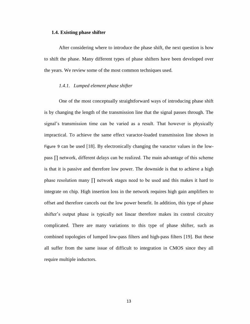
1.4. Existing phase shifter
After considering where to introduce the phase shift, the next question is how
to shift the phase. Many different types of phase shifters have been developed over
the years. We review some of the most common techniques used.
1.4.1. Lumped element phase shifter
One of the most conceptually straightforward ways of introducing phase shift
is by changing the length of the transmission line that the signal passes through. The
signal’s transmission time can be varied as a result. That however is physically
impractical. To achieve the same effect varactor-loaded transmission line shown in
Figure 9 can be used [18]. By electronically changing the varactor values in the low-
pass ∏ network, different delays can be realized. The main advantage of this scheme
is that it is passive and therefore low power. The downside is that to achieve a high
phase resolution many ∏ network stages need to be used and this makes it hard to
integrate on chip. High insertion loss in the network requires high gain amplifiers to
offset and therefore cancels out the low power benefit. In addition, this type of phase
shifter’s output phase is typically not linear therefore makes its control circuitry
complicated. There are many variations to this type of phase shifter, such as
combined topologies of lumped low-pass filters and high-pass filters [19]. But these
all suffer from the same issue of difficult to integration in CMOS since they all
require multiple inductors.
14
Figure 9: Varactor-loaded transmission line phase shifter
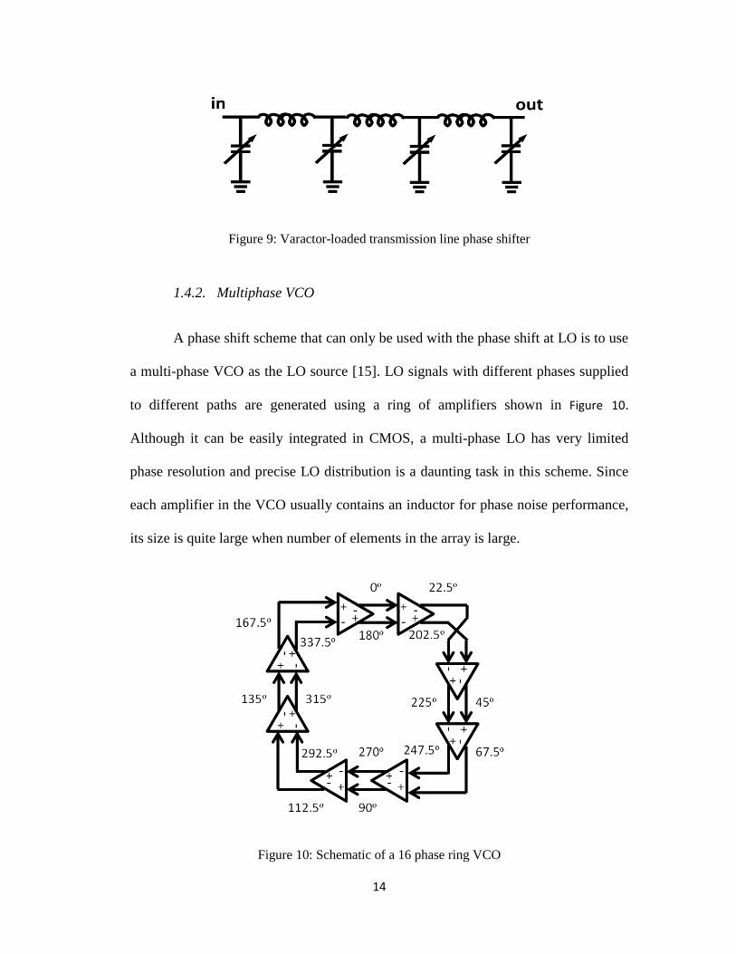
1.4.2. Multiphase VCO
A phase shift scheme that can only be used with the phase shift at LO is to use
a multi-phase VCO as the LO source [15]. LO signals with different phases supplied
to different paths are generated using a ring of amplifiers shown in Figure 10.
Although it can be easily integrated in CMOS, a multi-phase LO has very limited
phase resolution and precise LO distribution is a daunting task in this scheme. Since
each amplifier in the VCO usually contains an inductor for phase noise performance,
its size is quite large when number of elements in the array is large.
Figure 10: Schematic of a 16 phase ring VCO
15
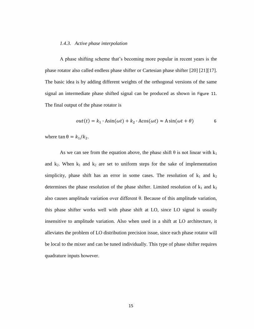
1.4.3. Active phase interpolation
A phase shifting scheme that’s becoming more popular in recent years is the
phase rotator also called endless phase shifter or Cartesian phase shifter [20] [21][17].
The basic idea is by adding different weights of the orthogonal versions of the same
signal an intermediate phase shifted signal can be produced as shown in Figure 11.
The final output of the phase rotator is
6
where .
As we can see from the equation above, the phase shift θ is not linear with k1
and k2. When k1 and k2 are set to uniform steps for the sake of implementation
simplicity, phase shift has an error in some cases. The resolution of k1 and k2
determines the phase resolution of the phase shifter. Limited resolution of k1 and k2
also causes amplitude variation over different θ. Because of this amplitude variation,
this phase shifter works well with phase shift at LO, since LO signal is usually
insensitive to amplitude variation. Also when used in a shift at LO architecture, it
alleviates the problem of LO distribution precision issue, since each phase rotator will
be local to the mixer and can be tuned individually. This type of phase shifter requires
quadrature inputs however.
16
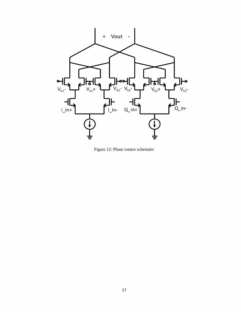
Figure 11: Phase interpolation scheme
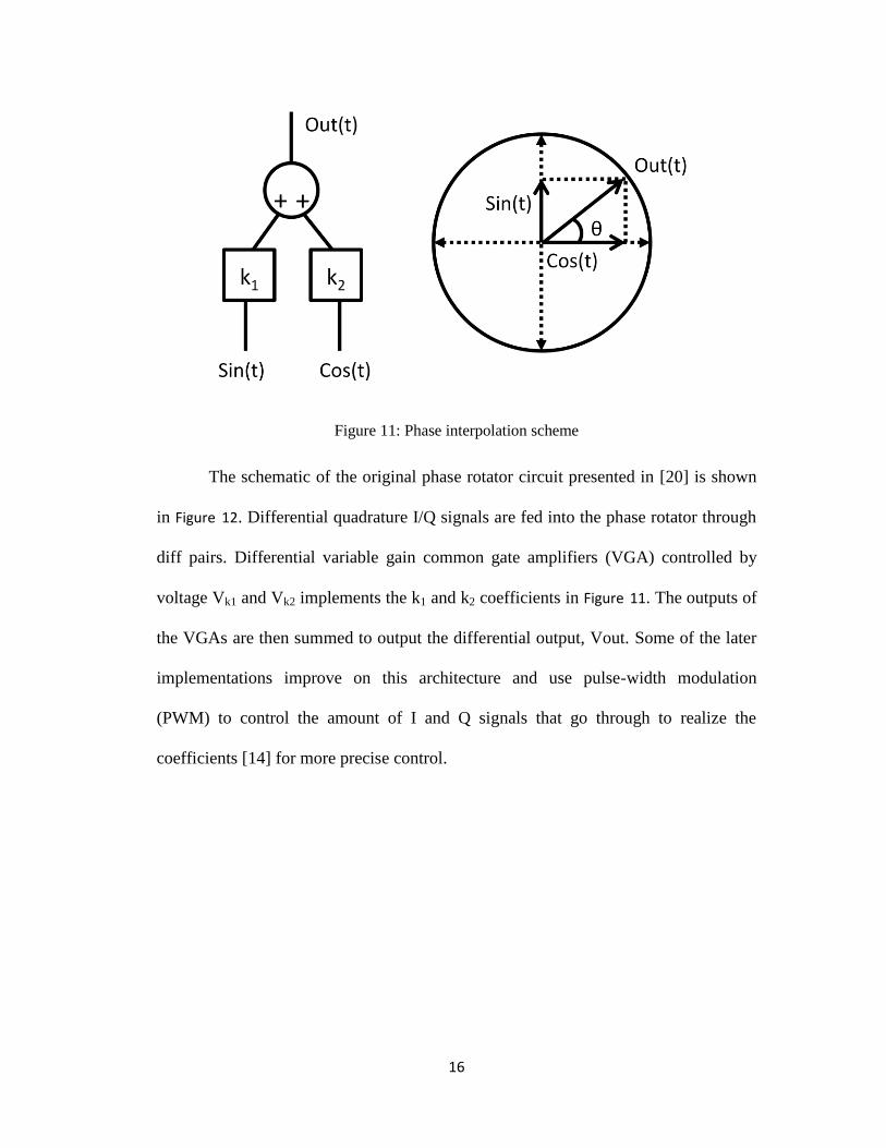
The schematic of the original phase rotator circuit presented in [20] is shown
in Figure 12. Differential quadrature I/Q signals are fed into the phase rotator through
diff pairs. Differential variable gain common gate amplifiers (VGA) controlled by
voltage Vk1 and Vk2 implements the k1 and k2 coefficients in Figure 11. The outputs of
the VGAs are then summed to output the differential output, Vout. Some of the later
implementations improve on this architecture and use pulse-width modulation
(PWM) to control the amount of I and Q signals that go through to realize the
coefficients [14] for more precise control.
17
Figure 12: Phase rotator schematic
18
1.5. Conclusion
From discussion above, we can see that each of the three phase shift
architectures have their own advantages and disadvantages and thus need to be used
in conjunction with appropriate phase shifter. For shift at RF, the lumped elements
phase shifter is the best choice, since at very high frequency passive elements used
are small and their performance is very linear [13]. For shift at DC, the phase rotator
is a good choice since it does not use any large passive components whose sizes are
inversely proportional to frequency, therefore more CMOS compatible [14]. For shift
at LO, the phase rotator is also a good choice, since LO is insensitive to insertion loss
and other non-idealities caused by high frequency [9][16].
This thesis focuses mainly on phased arrays with frequency lower than mm-
wave range thus we do not compare with shift at RF. For shift at DC and LO, the
disadvantages of using the phase rotator are mainly the non-linearity of output phase
versus control signal and the requirement for quadrature inputs. When used in phase
shift at DC, noise performance becomes an issue. When used in shift at LO,
distribution of high frequency LO signals is a problem. Although the LO signal’s
phase delay is not as important in shift at LO, distributing a signal close to RF
frequency can still be difficult and power consuming. This thesis presents an
architecture utilizing PLLs that solves these issues while retaining most of its
benefits.
19
Chapter 2
PLL Basics
2.1. Introduction to PLL
The concept of phase locked loop (PLL) was first developed in the 1930’s
[22]. Since then, it has been widely used in a wide range of applications from
communication to clock generation and many more. In essence a phase lock loop is a
feedback control system that generates an output signal whose phase is locked to the
input reference phase. Just like in an op-amp, by changing the feedback factor, output
frequency is a multiple of the input frequency. The core components include a phase
frequency detector (PFD), loop filter, a voltage controlled oscillator (VCO) and a
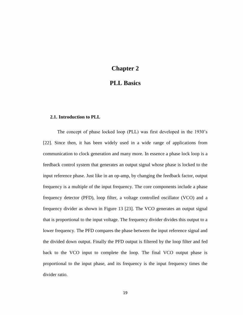
frequency divider as shown in Figure 13 [23]. The VCO generates an output signal
that is proportional to the input voltage. The frequency divider divides this output to a
lower frequency. The PFD compares the phase between the input reference signal and
the divided down output. Finally the PFD output is filtered by the loop filter and fed
back to the VCO input to complete the loop. The final VCO output phase is
proportional to the input phase, and its frequency is the input frequency times the
divider ratio.
20
Figure 13: Simple PLL block diagram
A linear model of the PLL is shown in Figure 14. The phase detector is
represented as Kpd with units of V/rad. Since its function is to linearly transfer phase
information to a voltage, therefore it’s just a linear gain element in the system. The
loop filter is presented by its transfer function F(s). A different F(s) changes the PLL
behavior as we will discuss later. The VCO is represented by a gain block Kvco with
units of Hz/V and an integrator. The VCO’s input is a voltage representation of phase
error information, but its output is frequency. Since phase is integral of frequency, a
VCO has an innate integration. And finally the frequency divider divides phase
linearly, and therefore is represented as 1/N, where N is the divide ratio.
Figure 14: Linear PLL model
21
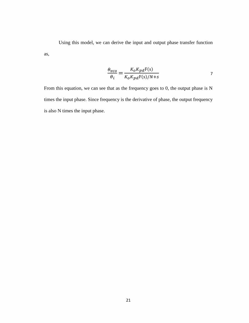
Using this model, we can derive the input and output phase transfer function
as,
7
From this equation, we can see that as the frequency goes to 0, the output phase is N
times the input phase. Since frequency is the derivative of phase, the output frequency
is also N times the input phase.
22
2.2. Traditional charge-pump phase detector
Figure 15: Charge-pump PLL schematic
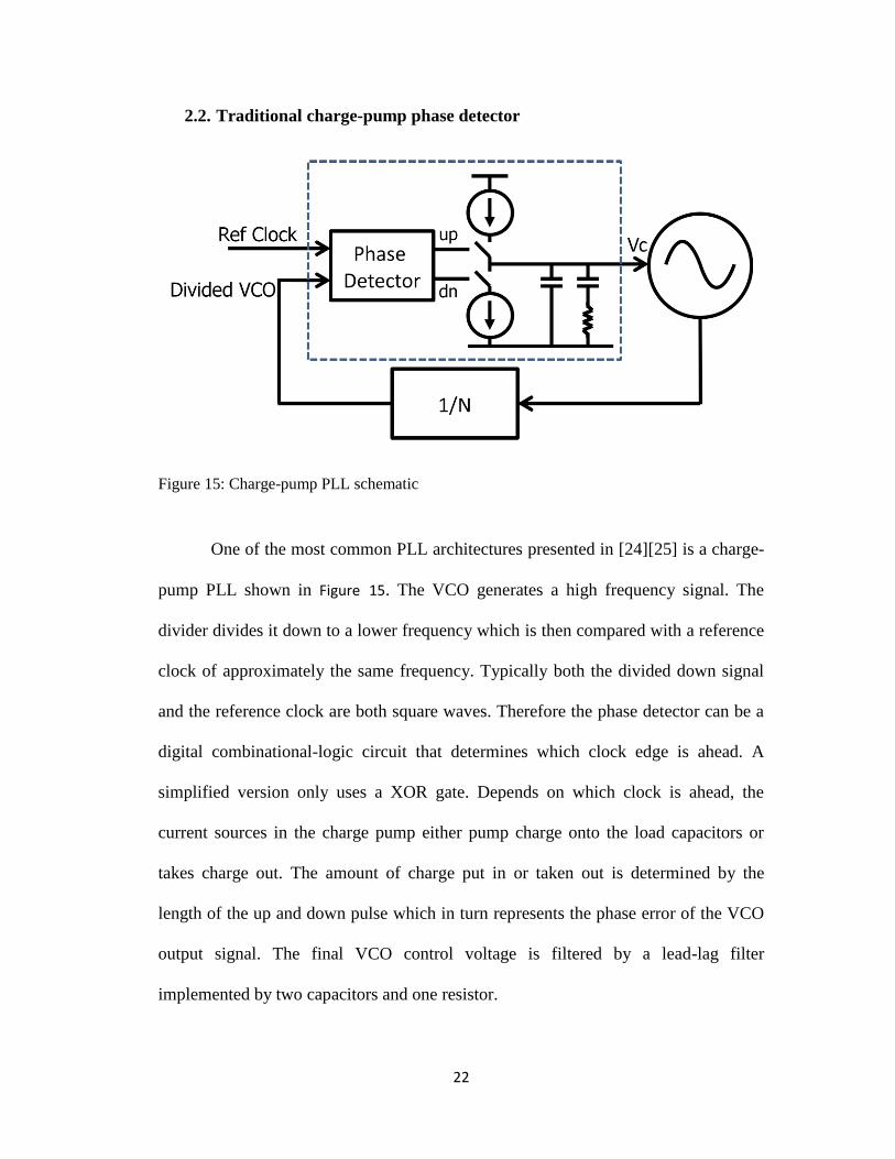
One of the most common PLL architectures presented in [24][25] is a charge-
pump PLL shown in Figure 15. The VCO generates a high frequency signal. The
divider divides it down to a lower frequency which is then compared with a reference
clock of approximately the same frequency. Typically both the divided down signal
and the reference clock are both square waves. Therefore the phase detector can be a
digital combinational-logic circuit that determines which clock edge is ahead. A
simplified version only uses a XOR gate. Depends on which clock is ahead, the
current sources in the charge pump either pump charge onto the load capacitors or
takes charge out. The amount of charge put in or taken out is determined by the
length of the up and down pulse which in turn represents the phase error of the VCO
output signal. The final VCO control voltage is filtered by a lead-lag filter
implemented by two capacitors and one resistor.
23
The biggest drawback of this architecture is the phase detector/charge
pump/filter circuitry shown in dotted box in Figure 15 is analog intensive and prone to
mismatch and process variation. The exact current output of the two current sources
has to be very accurate, since phase detector gain Kpd in this case is Icp/2π, where Icp
is the charge pump current. Although the phase detector is a digital circuit, the phase
information represented by the length of the up and down pulse is still an analog
signal and needs to be very accurate. Charge can also feed through to the integration
capacitor when the up and down switches switch [26].
24
2.3. Type I PLL vs. Type II PLL
A Type I PLL has one integrator in its open loop transfer function. Normally
this integrator is the VCO, which converts input frequency into phase. Since phase is
the integral of frequency, the VCO acts as an integrator as discussed earlier. On the
other hand, a Type II PLL has two integrators. Beside the VCO, it also has an
integrator in the loop filter. A Type II PLL forces the steady state phase detector error
to zero because the phase error is integrated by the additional integral. Due to this
high pass effect, a Type II PLL also suppresses close to carrier up-converted flicker
noise. However Type II loops are harder to design and require a stabilizing zero.
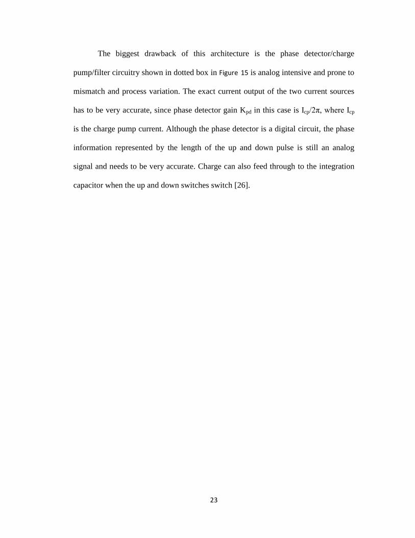
Figure 16: Simplified charge pump loop filter
The conventional Type II PLL architecture is shown in Figure 15. Looking at
its loop filter in Figure 16, the charge pump and C2 forms an integrator in the loop.
This extra integrator makes this architecture Type II. The resistor R1 in series with C2
introduces a stabilizing zero. Moreover a smaller capacitor C1 is added in parallel to
smooth out the ripple caused by the addition of R1. The final loop filter transfer
function is given in [25] as,
25
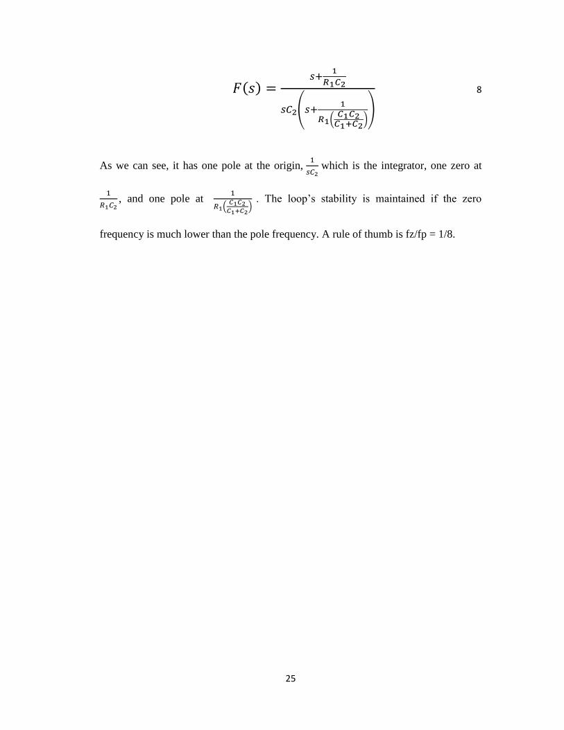
8
As we can see, it has one pole at the origin,
which is the integrator, one zero at
, and one pole at
. The loop’s stability is maintained if the zero
frequency is much lower than the pole frequency. A rule of thumb is fz/fp = 1/8.
26
2.4. Fractional-N divider
In all the discussions above the frequency divide ratio is always an integer N,
because integer division is easy to achieve in CMOS since it is simply a digital
counter. But fine output frequency step is important for selecting the right band for
telecommunication purposes and for other applications. We could use a small
reference value. However that is impractical, because PLL is a sampled system. We
can think of phase error as being sampled at the PFD by the reference signal. To
avoid aliasing, a reference frequency higher than the loop bandwidth is needed.
Therefore we cannot use an arbitrary low reference frequency and thus fractional
divide ratio is necessary.
One of the first attempts to implement a fractional divider is switching
between different integer divide ratios. This way a fractional divide ratio can be
achieved. For example, by switching between divide ratios of 1, 2, 1, 2…, the
resulting average divide ratio is 1.5. However this type of highly repetitive pattern
causes fractional spurs in the PLL’s output.
A better way to switch divide ratio is to use a ΣΔ modulator. In this case the
PLL is referred to as a ΣΔ fractional-N PLL. A ΣΔ modulator converts a high
precision value into a stream of quantized lower precision values and keeps the
output’s average equal to the input. A simple first order ΣΔ modulator and its typical
output when fed a constant decimal value are shown in Figure 17. We can see from the
output that a constant input of 12.368746 is converted to a stream of 12s and 13s. The
average of the stream is still 12.368746 and no obvious periodicity can be seen from
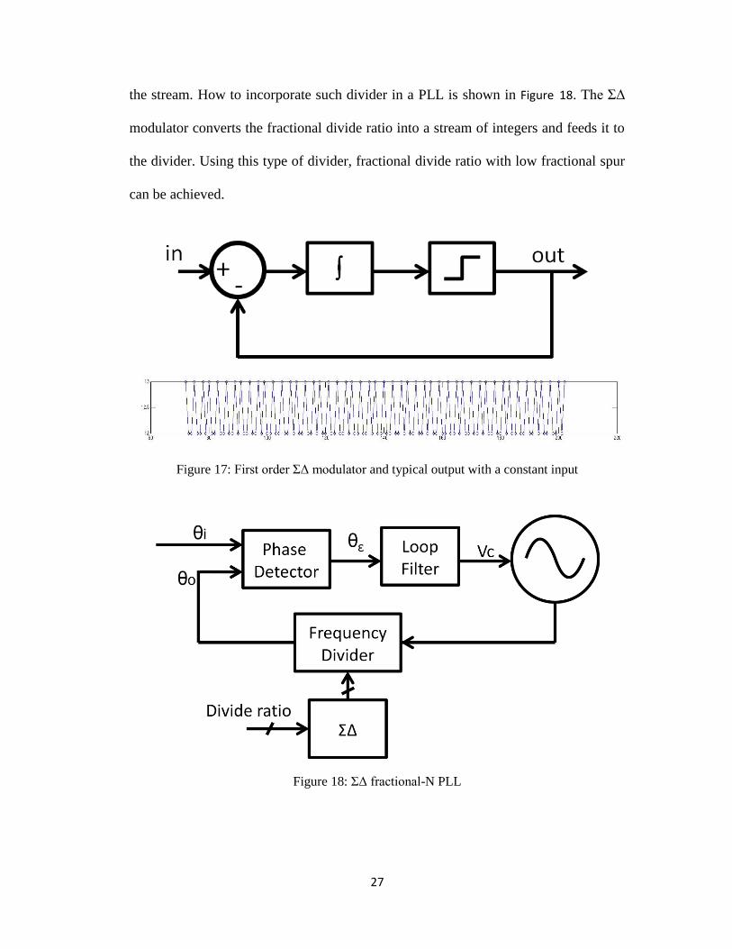
27
the stream. How to incorporate such divider in a PLL is shown in Figure 18. The ΣΔ
modulator converts the fractional divide ratio into a stream of integers and feeds it to
the divider. Using this type of divider, fractional divide ratio with low fractional spur
can be achieved.
Figure 17: First order ΣΔ modulator and typical output with a constant input
Figure 18: ΣΔ fractional-N PLL
28
2.5. PLL phase noise analysis
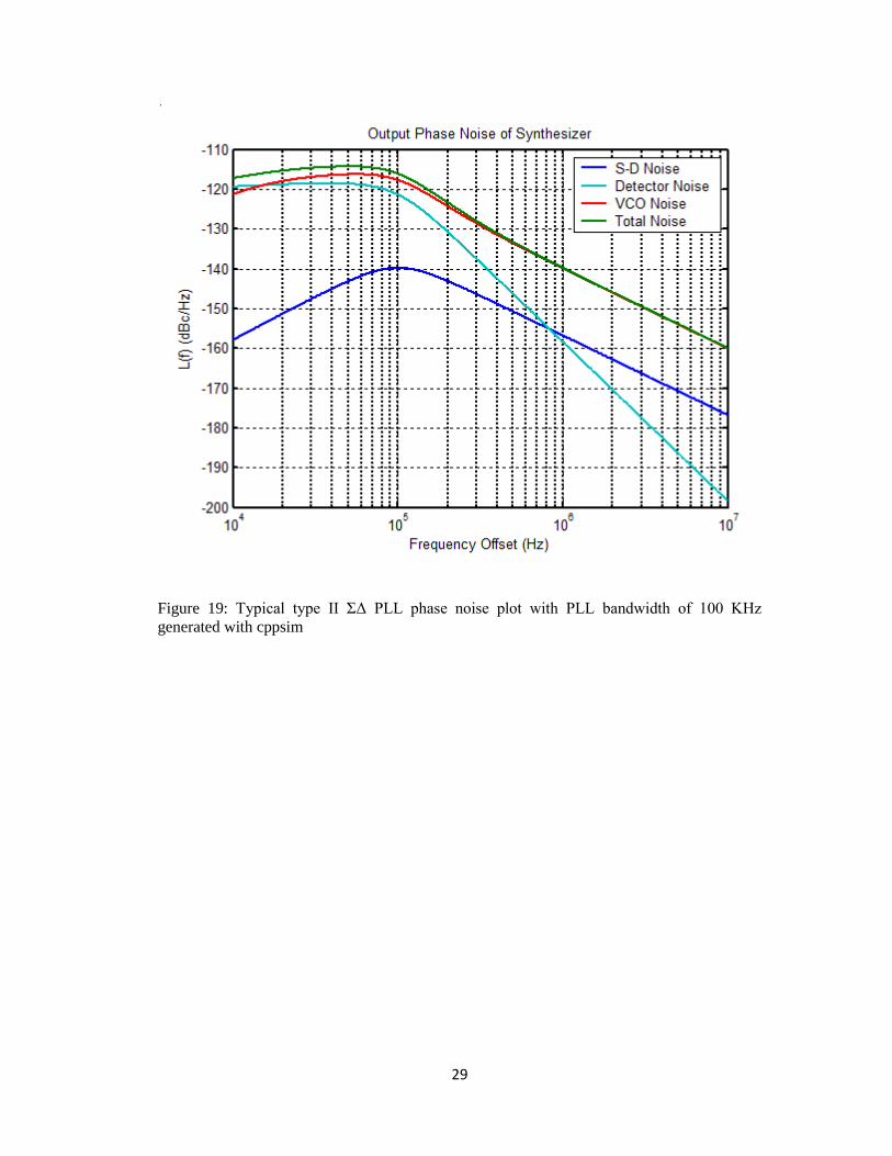
Typically a ΣΔ PLL has three main sources of phase noise, VCO noise, PFD
noise and ΣΔ noise. VCO noise and PFD noise are common to all PLLs. Their origin
can be thermal noise, 1/f noise, or digital switching noise. ΣΔ noise is quantization
noise associated with the ΣΔ modulator used in the divider. A typical Type II ΣΔ PLL
phase noise plot is shown in Figure 19. The PLL bandwidth is 100 kHz in this example.
PFD noise spectrum is generally flat. The loop simply acts as a low pass filter and
attenuates the PFD noise outside the bandwidth. A ΣΔ modulator has noise shaping
effect that pushes noise to higher frequency. Therefore ΣΔ noise spectrum has high
pass behavior. However ΣΔ noise is also low pass filtered by the loop, the combined
effect is a band pass response. A free-running VCO’s phase noise linearly decreases
20dB/decade, if we ignore 1/f noise. VCO noise however is not low pass filtered, but
high pass filtered. This is because VCO noise adds directly to the output. Intuitively,
the feedback loop will try to keep the output aligned. Inside the bandwidth, the gain is
high enough to minimize the error, but outside the feedback loop won’t be fast
enough to suppress the error. Therefore as can be seen in Figure 19, the VCO noise
contribution is attenuated inside the PLL bandwidth, but not outside. Overall, a higher
bandwidth suppresses more VCO noise, but at the same time it lets through more
PFD noise and ΣΔ noise. Thus there is a PLL bandwidth where total phase noise is
minimized.
29
Figure 19: Typical type II ΣΔ PLL phase noise plot with PLL bandwidth of 100 KHz
generated with cppsim
30
Chapter 3
Phase-Setting PLL
3.1. Background
Accurate phase control of high-speed signals is required in serial links, radar,
beam-steering and medical imaging systems. CMOS integrated phased-array
transceivers offer enormous possibilities for secure, low cost wireless communication
systems [9][15][3]. One of the main challenges in realizing these applications in
CMOS is the implementation of a precise, flexible, and physically small phase shifter.
Multi-phase VCOs haves limited resolution, RF phase shifters are expansive and hard
to design, and baseband phase shifters require bulky components. On the other hand,
phase interpolation requires quadrature inputs, has limited linearity and is prone to
phase error due to amplitude variation.
We present a digital PLL architecture that can make precise high-resolution
steps in phase of its output signal. Here phase control is implemented in the digital
domain; no additional analog circuits are required other than the PLL itself. This
phase generation mechanism consumes little power, and it does not affect the phase
noise of the PLL.
31
3.2. Overview of phase control mechanism
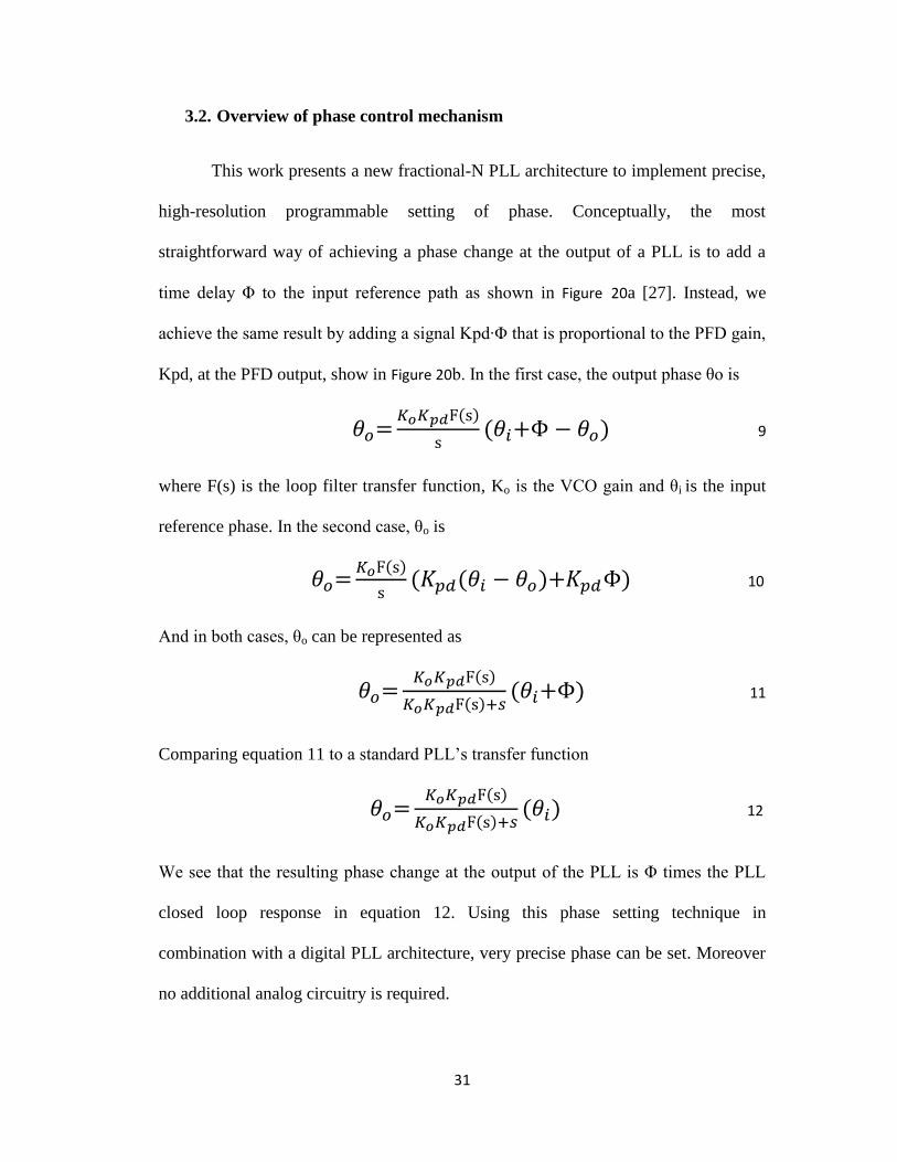
This work presents a new fractional-N PLL architecture to implement precise,
high-resolution programmable setting of phase. Conceptually, the most
straightforward way of achieving a phase change at the output of a PLL is to add a
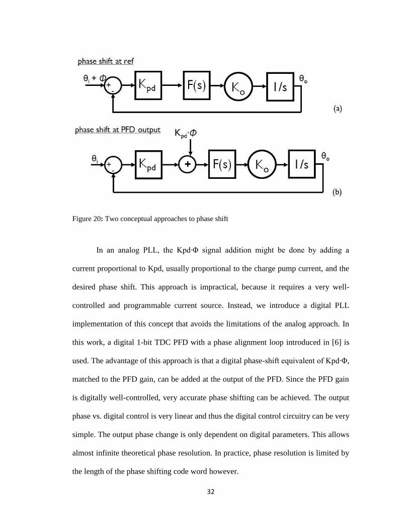
time delay Φ to the input reference path as shown in Figure 20a [27]. Instead, we
achieve the same result by adding a signal Kpd∙Φ that is proportional to the PFD gain,
Kpd, at the PFD output, show in Figure 20b. In the first case, the output phase θo is
9
where F(s) is the loop filter transfer function, Ko is the VCO gain and θi is the input
reference phase. In the second case, θo is
10
And in both cases, θo can be represented as
11
Comparing equation 11 to a standard PLL’s transfer function
12
We see that the resulting phase change at the output of the PLL is Φ times the PLL
closed loop response in equation 12. Using this phase setting technique in
combination with a digital PLL architecture, very precise phase can be set. Moreover
no additional analog circuitry is required.
32
Figure 20: Two conceptual approaches to phase shift
In an analog PLL, the Kpd∙Φ signal addition might be done by adding a
current proportional to Kpd, usually proportional to the charge pump current, and the
desired phase shift. This approach is impractical, because it requires a very well-
controlled and programmable current source. Instead, we introduce a digital PLL
implementation of this concept that avoids the limitations of the analog approach. In
this work, a digital 1-bit TDC PFD with a phase alignment loop introduced in [6] is
used. The advantage of this approach is that a digital phase-shift equivalent of Kpd∙Φ,
matched to the PFD gain, can be added at the output of the PFD. Since the PFD gain
is digitally well-controlled, very accurate phase shifting can be achieved. The output
phase vs. digital control is very linear and thus the digital control circuitry can be very
simple. The output phase change is only dependent on digital parameters. This allows
almost infinite theoretical phase resolution. In practice, phase resolution is limited by
the length of the phase shifting code word however.
33
3.3. PLL architecture
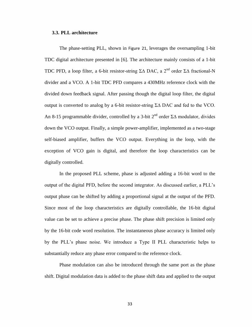
The phase-setting PLL, shown in Figure 21, leverages the oversampling 1-bit
TDC digital architecture presented in [6]. The architecture mainly consists of a 1-bit
TDC PFD, a loop filter, a 6-bit resistor-string Σ∆ DAC, a 2nd
order Σ∆ fractional-N
divider and a VCO. A 1-bit TDC PFD compares a 430MHz reference clock with the
divided down feedback signal. After passing though the digital loop filter, the digital
output is converted to analog by a 6-bit resistor-string Σ∆ DAC and fed to the VCO.
An 8-15 programmable divider, controlled by a 3-bit 2nd
order Σ∆ modulator, divides
down the VCO output. Finally, a simple power-amplifier, implemented as a two-stage
self-biased amplifier, buffers the VCO output. Everything in the loop, with the
exception of VCO gain is digital, and therefore the loop characteristics can be
digitally controlled.
In the proposed PLL scheme, phase is adjusted adding a 16-bit word to the
output of the digital PFD, before the second integrator. As discussed earlier, a PLL’s
output phase can be shifted by adding a proportional signal at the output of the PFD.
Since most of the loop characteristics are digitally controllable, the 16-bit digital
value can be set to achieve a precise phase. The phase shift precision is limited only
by the 16-bit code word resolution. The instantaneous phase accuracy is limited only
by the PLL’s phase noise. We introduce a Type II PLL characteristic helps to
substantially reduce any phase error compared to the reference clock.
Phase modulation can also be introduced through the same port as the phase
shift. Digital modulation data is added to the phase shift data and applied to the output
34
of the PFD. Consequently the PLL can employ both phase modulation and phase
setting. Next we will go through each block in detail.
Figure 21: PLL modulator architecture
3.3.1. 1-bit TDC PFD
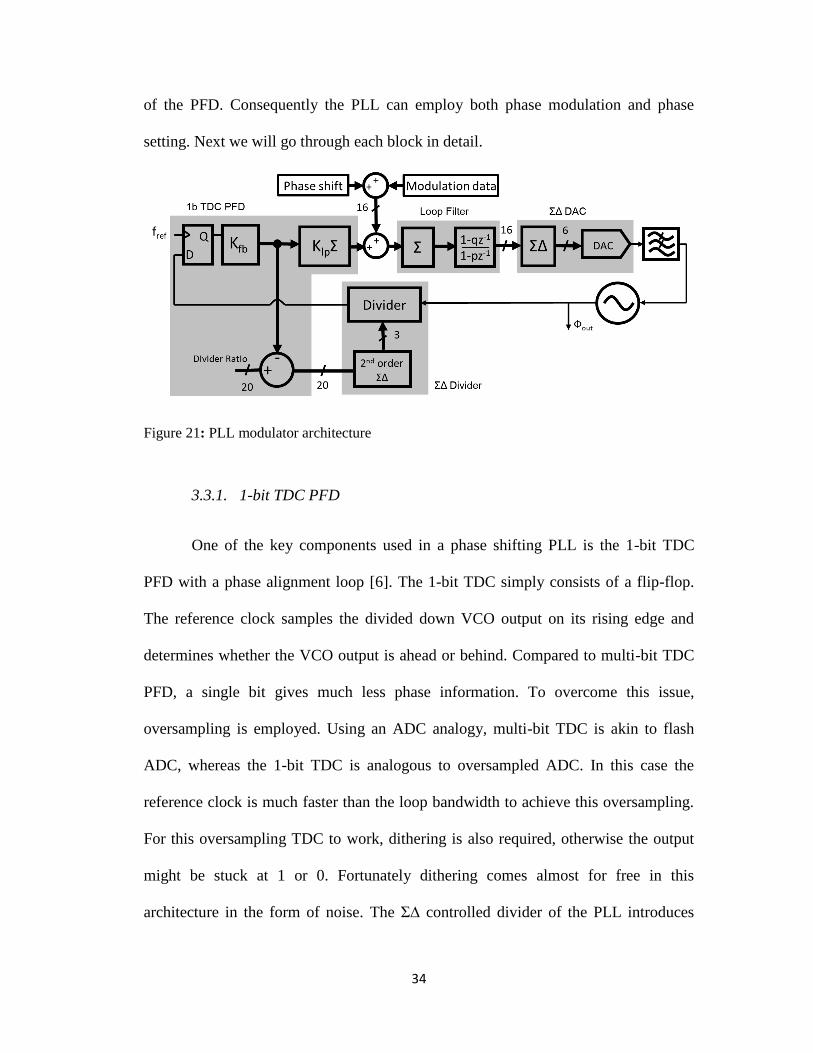
One of the key components used in a phase shifting PLL is the 1-bit TDC
PFD with a phase alignment loop [6]. The 1-bit TDC simply consists of a flip-flop.
The reference clock samples the divided down VCO output on its rising edge and
determines whether the VCO output is ahead or behind. Compared to multi-bit TDC
PFD, a single bit gives much less phase information. To overcome this issue,
oversampling is employed. Using an ADC analogy, multi-bit TDC is akin to flash
ADC, whereas the 1-bit TDC is analogous to oversampled ADC. In this case the
reference clock is much faster than the loop bandwidth to achieve this oversampling.
For this oversampling TDC to work, dithering is also required, otherwise the output
might be stuck at 1 or 0. Fortunately dithering comes almost for free in this
architecture in the form of noise. The Σ∆ controlled divider of the PLL introduces
35
significant Σ∆ noise to the divided down VCO output and dithers the signal. The final
output of the TDC is filtered to remove the Σ∆ noise. This PFD can also be seen as a
type of bang-bang PFD.
Additionally a feedback loop shown in Figure 22 is added to minimize the
phase difference between the reference clock and the divided down clock. If the phase
difference is too large, the 1-bit TDC will rail to 1 or 0. The output of the TDC phase
detector is scaled by a factor, Kfb and fed back to the divider ratio input. The feedback
signal is subtracted from the divide ratio. If the phase detector indicates that the
divided down clock is ahead, in which case the feedback signal is positive, then a
lower the divide ratio slows it down, if it is behind, in which case the signal is
negative, then an increase in the divide ratio speeds it up. This feedback loop keeps
the phase difference small and keeps that output of the phase detector from railing.
Figure 22: 1-bit TDC PFD block diagram
36
3.3.2. PLL Type
We would like to use a Type II PLL for phase setting operation. As discussed
in section 2.3, a Type II PLL removes the dc phase error associated with a Type I
PLL. The key to achieve a Type II PLL is to have two integrators in the loop. At first
glance, it appears that the 1-bit TDC PFD contains an integrator and therefore no
additional integrator is necessary in the loop filter. However upon closer examination,
we see that the feedback loop in the PFD introduces a differentiation in the loop and
cancels the integration. In Figure 22, the output of the Kfb block represents phase
information, but it is subtracted from the divider ratio, which controls frequency.
Phase is the integral of frequency. Integration in the feedback loop causes a
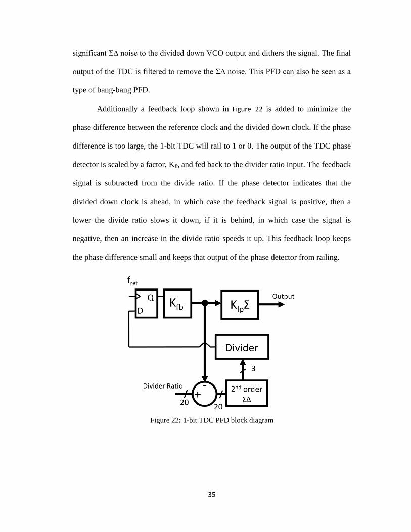
differentiation in the whole loop. This can be seen from Figure 23. The transfer
function of this system is
13
Simplifying we get
14
This transfer function consists of two components, the differentiation part s in the
numerator and a pole at -A in the denominator. If A is sufficiently large so that the
pole is higher in frequency than most other poles in the system, the pole can be
ignored leaving only the differentiation component. Therefore without another
integrator in the loop, a PLL using this PFD is Type I, as in [6]. However there is no
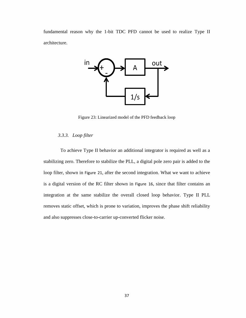
37
fundamental reason why the 1-bit TDC PFD cannot be used to realize Type II
architecture.
Figure 23: Linearized model of the PFD feedback loop
3.3.3. Loop filter
To achieve Type II behavior an additional integrator is required as well as a
stabilizing zero. Therefore to stabilize the PLL, a digital pole zero pair is added to the
loop filter, shown in Figure 21, after the second integration. What we want to achieve
is a digital version of the RC filter shown in Figure 16, since that filter contains an
integration at the same stabilize the overall closed loop behavior. Type II PLL
removes static offset, which is prone to variation, improves the phase shift reliability
and also suppresses close-to-carrier up-converted flicker noise.
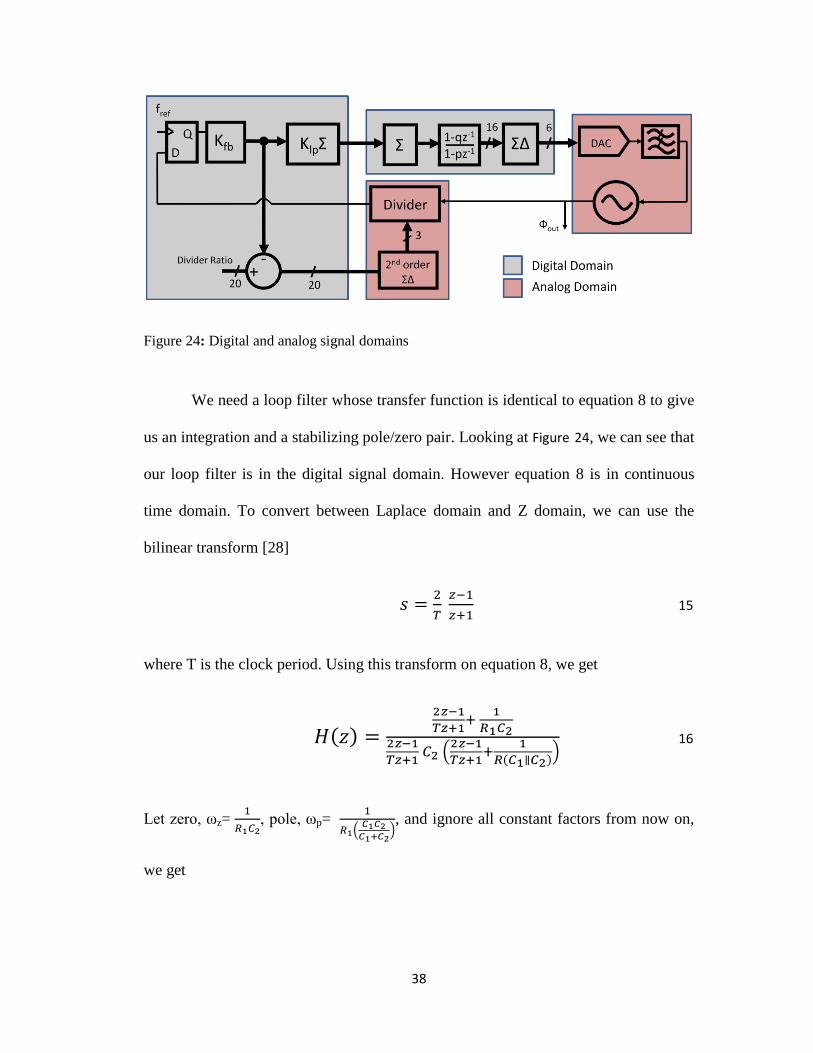
38
Figure 24: Digital and analog signal domains
We need a loop filter whose transfer function is identical to equation 8 to give
us an integration and a stabilizing pole/zero pair. Looking at Figure 24, we can see that
our loop filter is in the digital signal domain. However equation 8 is in continuous
time domain. To convert between Laplace domain and Z domain, we can use the
bilinear transform [28]
15
where T is the clock period. Using this transform on equation 8, we get
16
Let zero, ωz=
, pole, ωp=
, and ignore all constant factors from now on,
we get
39
17
We can separate the integral part and the pole zero pair, and then simplify.
18
Converting everything to the form z-1
we get
19
What we have is an integrator
, a zero q1 at
, and a pole p1 at
. ωz
and ωp are pole zero frequencies in a traditional Type II PLL. Using this transfer
function, pole/zero values and open loop gain can be chosen appropriately for the
required bandwidth. By plotting its gain and phase Bode plots, using the basic phase
margin criterion, loop stability can be inferred. In practice, these values can be
calculated using cppsim. Cppsim utilizes a close loop approach algorism, which
determines the close loop response of the transfer function based on desired criteria
such as loop bandwidth. From the close loop transfer function, the open loop transfer
function is calculated and the loop filter transfer function is then derived [29]. After
obtaining the transfer function, we need to implement it in digital circuitry. We
40
separate the integrator and the pole zero pair into two blocks. Since the transfer
function is basically output divided by input,
20
We can substitute in the transfer function and get
21
22
23
z-1
is delay by one time step in the z domain. Therefore the output is the un-weighted
sum of the current input, the previous input, and the previous output. However if we
simply implement this in digital, we will have an issue. Because the PFD block before
the integrator KlpΣ in Figure 24 outputs an unsigned value, if we simply accumulate the
inputs, the output will monotonically increase and overflow. Therefore we offset the
unsigned value to the midpoint to create both positive and negative value.
Furthermore the previous input term, only introduces a FIR filter to the overall
function and doesn’t affect integration. After close loop simulation in both cppsim
and Spectre we found that this term can be ignored. Therefore the final output is
24
We can use the same method to obtain the equation for the pole zero pair.
41
25
26
Since a scaled version of the previous input is subtracted, the output is not
monotonically increasing and therefore does not overflow. Cascading the integrator
and the pole zero pair forms the digital equivalent of the loop filter shown in Figure 16.
This stability of the PLL is then verified with Spectre simulations. To verify
that the phase is stable, we look at the integral of the VCO’s control voltage. The
VCO control voltage is proportional to the frequency of the VCO and therefore its
integral is proportional to the phase. By looking at the integral of VCO control
voltage, which is proportional to the output phase, we can make sure that the loop is
settled with no significant ringing.
3.3.4. VCO
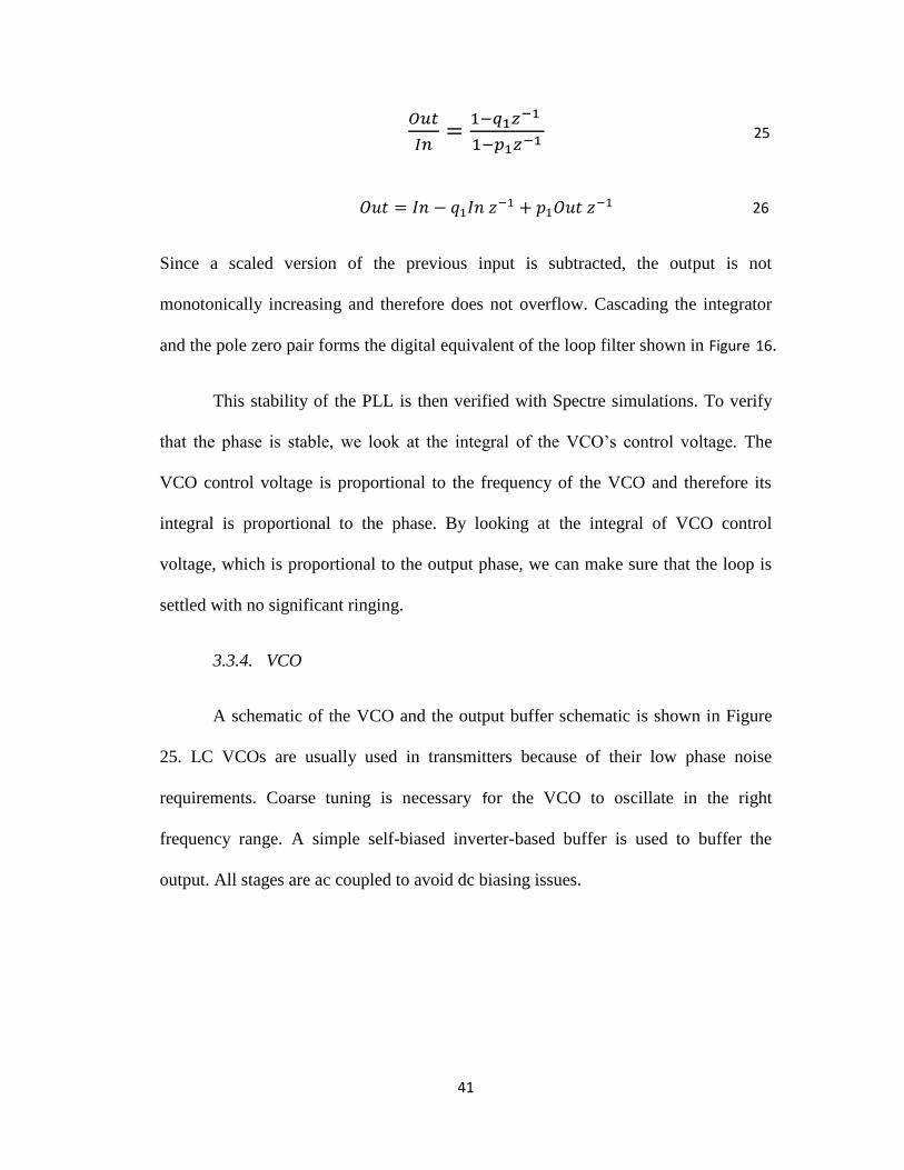
A schematic of the VCO and the output buffer schematic is shown in Figure
25. LC VCOs are usually used in transmitters because of their low phase noise
requirements. Coarse tuning is necessary for the VCO to oscillate in the right
frequency range. A simple self-biased inverter-based buffer is used to buffer the
output. All stages are ac coupled to avoid dc biasing issues.
42
Figure 25: VCO and output buffer schematics
43
3.4. Data modulation
To achieve a phased array transmitter, the system not only has to set output
phase, it also needs to be able to modulate data. In a PLL, there are several places
where output phase or frequency can be modulated. We discuss two of the
architectures that we examined.
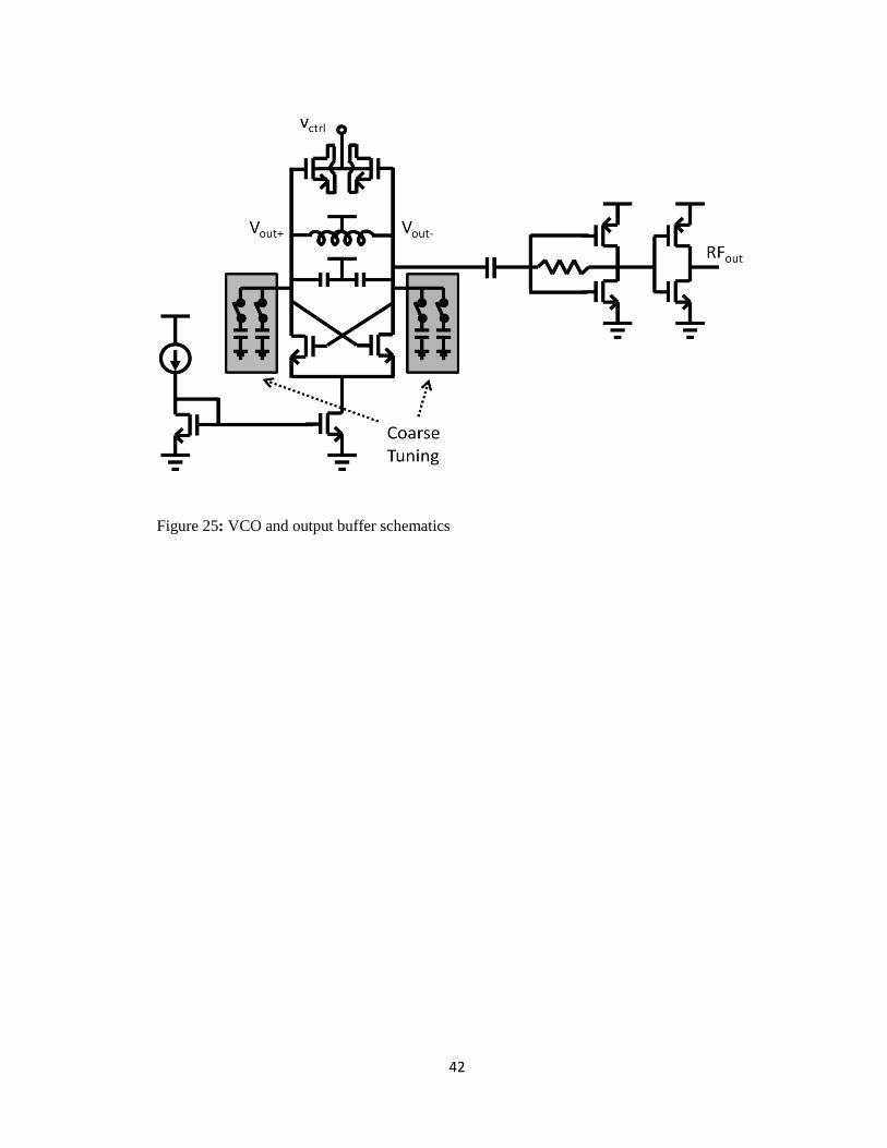
3.4.1. Divide ratio modulation
The most common data modulation method is frequency modulation by
changing the divider value as shown in Figure 26.
Figure 26: Divide ratio modulator
Since output frequency Vout is described by the following equation,
27
where N is the divide ratio and fref is the input reference frequency, by changing N we
can change the output frequency and perform FM or FSK.
44
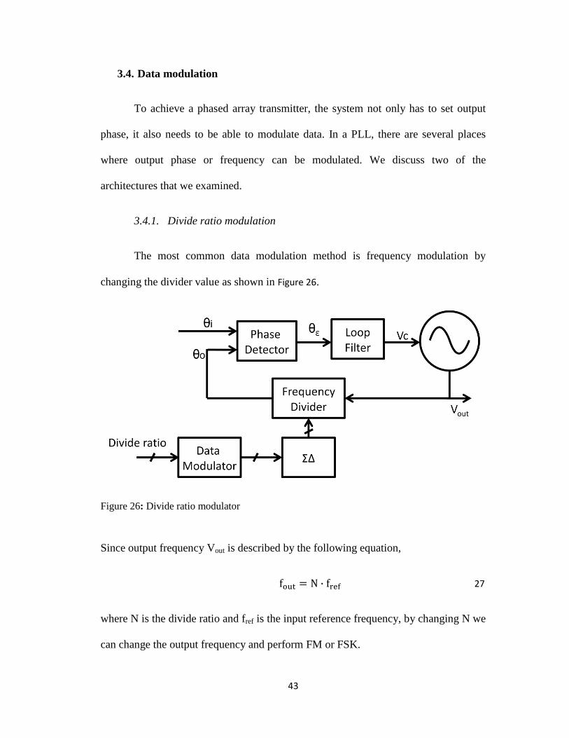
This modulation scheme has some issue when working in conjunction with
our phase-setting mechanism. Since during data transition when divide ratio is
changing, the loop is out of lock. During the relocking process, the final output phase
could potentially shift. This presents an issue for this architecture as it interferes with
phase setting. To overcome this issue, our first attempt was to split the roles of phase
shifting and data modulation into two different stages of cascaded PLLs as shown in
Figure 27. The first stage is a low frequency PLL responsible for phase-setting; the
second stage is a high frequency PLL responsible for data modulation. The first stage
of PLLs produces four phase-shifted reference signals. This reference is then feed
into the second stage, which modulates the signal. The two stage cascaded
architecture is able to combine the two functions in a single system.
Figure 27: two-stage cascading PLL architecture
45
However this architecture has a few major drawbacks. The biggest issue is its
large size and power consumption. By using two PLLs, we almost double the size and
power compared to a single PLL system. The design complexity is also immensely
increased. The second problem is increased phase noise. The phase noise of the first
stage is amplified by the second stage as explained in [30]. Due to these major issues,
this method is not a viable solution.
3.4.2. Direct phase modulation
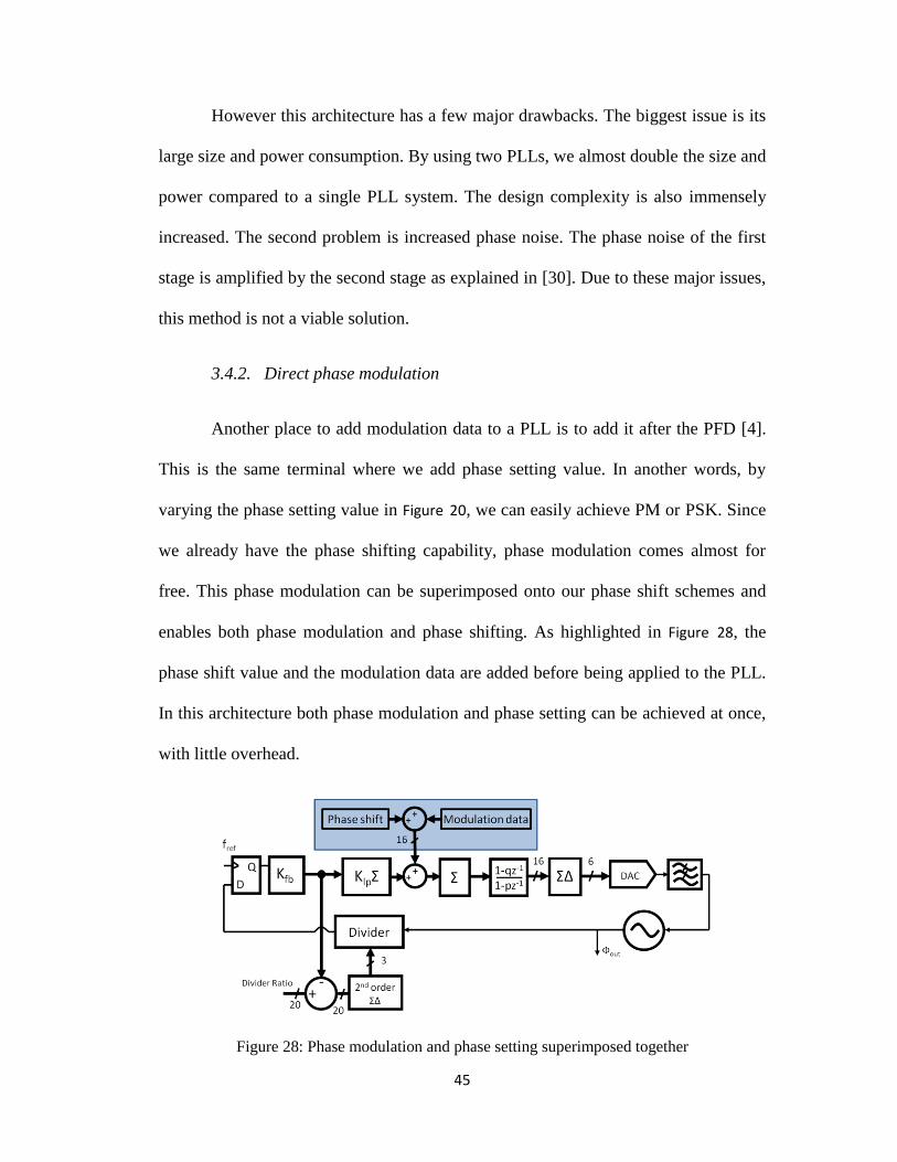
Another place to add modulation data to a PLL is to add it after the PFD [4].
This is the same terminal where we add phase setting value. In another words, by
varying the phase setting value in Figure 20, we can easily achieve PM or PSK. Since
we already have the phase shifting capability, phase modulation comes almost for
free. This phase modulation can be superimposed onto our phase shift schemes and
enables both phase modulation and phase shifting. As highlighted in Figure 28, the
phase shift value and the modulation data are added before being applied to the PLL.
In this architecture both phase modulation and phase setting can be achieved at once,
with little overhead.
Figure 28: Phase modulation and phase setting superimposed together
46
3.5. Phased array and conclusion
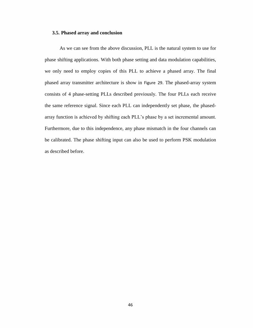
As we can see from the above discussion, PLL is the natural system to use for
phase shifting applications. With both phase setting and data modulation capabilities,
we only need to employ copies of this PLL to achieve a phased array. The final
phased array transmitter architecture is show in Figure 29. The phased-array system
consists of 4 phase-setting PLLs described previously. The four PLLs each receive
the same reference signal. Since each PLL can independently set phase, the phased-
array function is achieved by shifting each PLL’s phase by a set incremental amount.
Furthermore, due to this independence, any phase mismatch in the four channels can
be calibrated. The phase shifting input can also be used to perform PSK modulation
as described before.
47
Figure 29: Phased array system diagram
Overall the phased array system includes four 5.8GHz phase-setting PLLs
each capable of PSK modulation. Each channel has an output buffer that buffer the
output to a measureable signal level.
48
Chapter 4
Prototypes and Measurements
4.1. Overview
A total of three prototypes were implemented all in 65nm CMOS technology.
The first prototype is a 24GHz PLL phased array utilizing an architecture shown in
Figure 27. Due to the major drawbacks discuss earlier, a second prototype with an
updated architecture is fabricated. The second prototype is a 5.8GHz PLL phased
array with a PLL architecture shown in Figure 21. The third prototype is also a
5.8GHz PLL phased array with the same architecture as the second prototype aimed
at improving upon the second prototype’s performance.
49
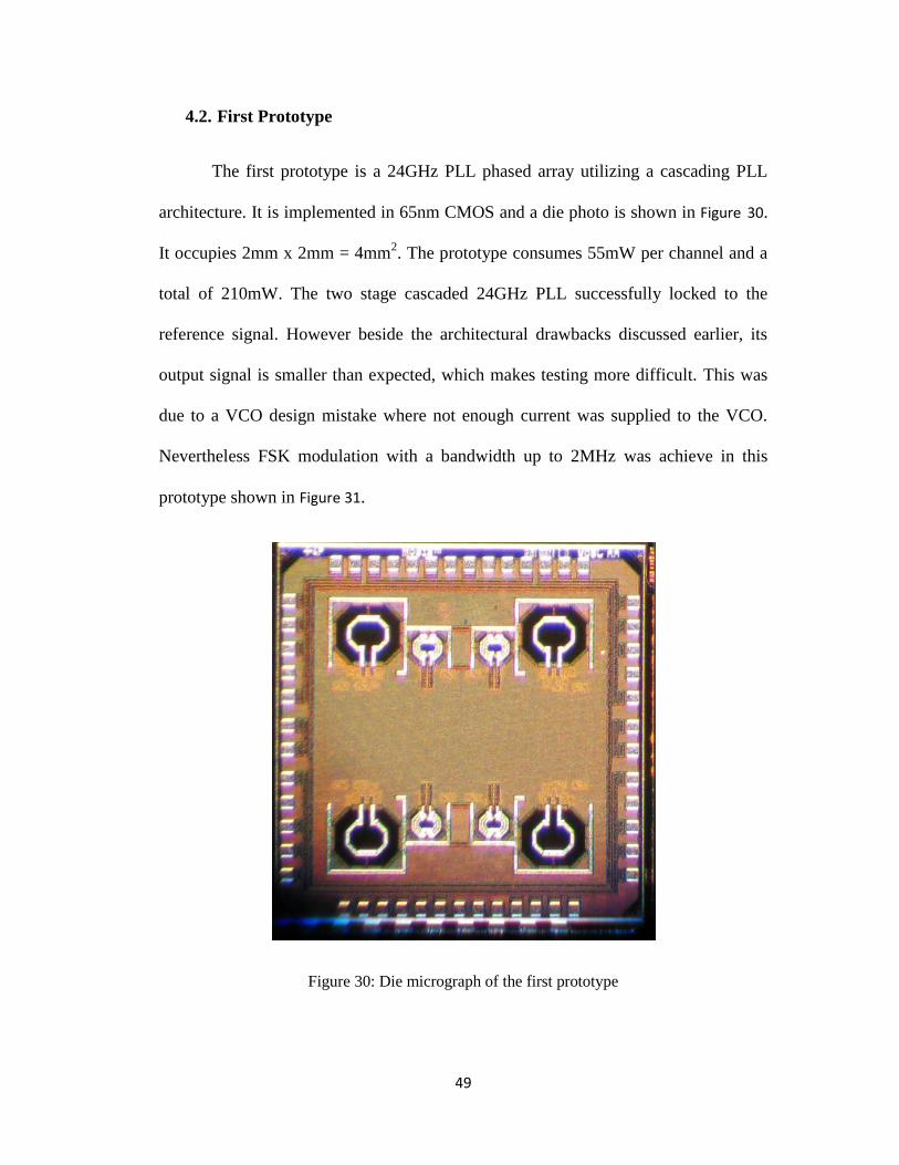
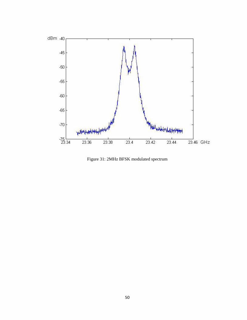
4.2. First Prototype
The first prototype is a 24GHz PLL phased array utilizing a cascading PLL
architecture. It is implemented in 65nm CMOS and a die photo is shown in Figure 30.
It occupies 2mm x 2mm = 4mm2. The prototype consumes 55mW per channel and a
total of 210mW. The two stage cascaded 24GHz PLL successfully locked to the
reference signal. However beside the architectural drawbacks discussed earlier, its
output signal is smaller than expected, which makes testing more difficult. This was
due to a VCO design mistake where not enough current was supplied to the VCO.
Nevertheless FSK modulation with a bandwidth up to 2MHz was achieve in this
prototype shown in Figure 31.
Figure 30: Die micrograph of the first prototype
50
Figure 31: 2MHz BFSK modulated spectrum
51
4.3. Second Prototype
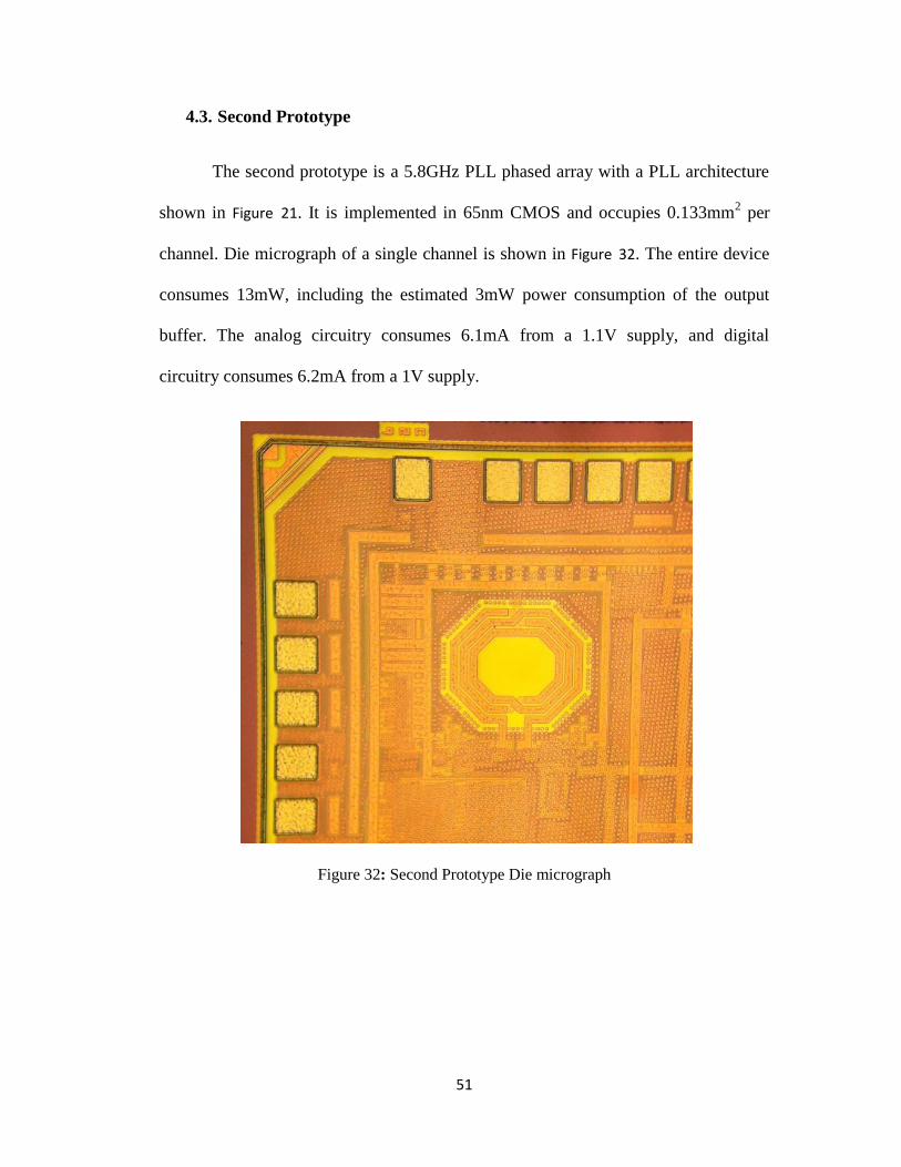
The second prototype is a 5.8GHz PLL phased array with a PLL architecture
shown in Figure 21. It is implemented in 65nm CMOS and occupies 0.133mm2 per
channel. Die micrograph of a single channel is shown in Figure 32. The entire device
consumes 13mW, including the estimated 3mW power consumption of the output
buffer. The analog circuitry consumes 6.1mA from a 1.1V supply, and digital
circuitry consumes 6.2mA from a 1V supply.
Figure 32: Second Prototype Die micrograph
52
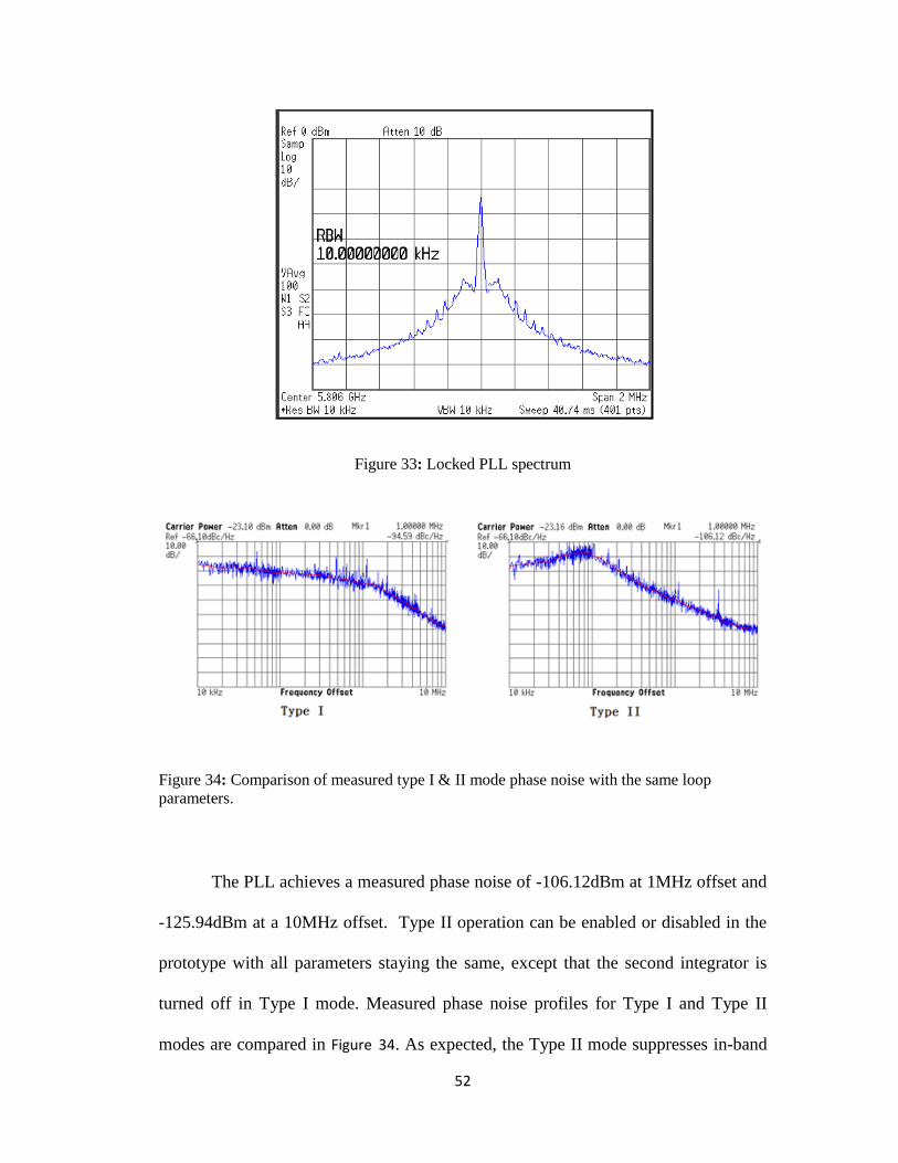
Figure 33: Locked PLL spectrum
Figure 34: Comparison of measured type I & II mode phase noise with the same loop
parameters.
The PLL achieves a measured phase noise of -106.12dBm at 1MHz offset and
-125.94dBm at a 10MHz offset. Type II operation can be enabled or disabled in the
prototype with all parameters staying the same, except that the second integrator is
turned off in Type I mode. Measured phase noise profiles for Type I and Type II
modes are compared in Figure 34. As expected, the Type II mode suppresses in-band
53
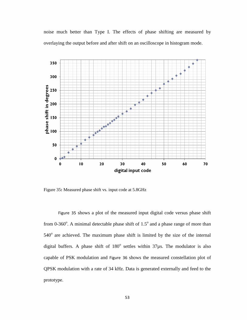
noise much better than Type I. The effects of phase shifting are measured by
overlaying the output before and after shift on an oscilloscope in histogram mode.
Figure 35: Measured phase shift vs. input code at 5.8GHz
Figure 35 shows a plot of the measured input digital code versus phase shift
from 0-360o. A minimal detectable phase shift of 1.5
o and a phase range of more than
540o are achieved. The maximum phase shift is limited by the size of the internal
digital buffers. A phase shift of 180o settles within 37µs. The modulator is also
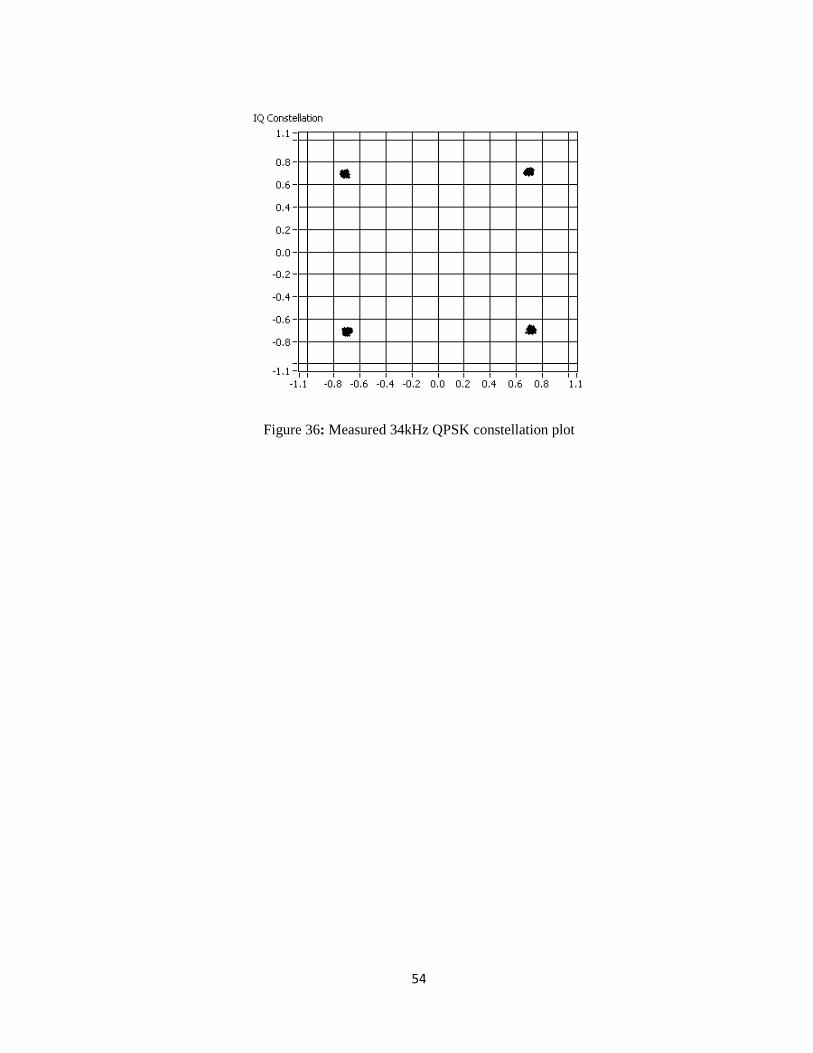
capable of PSK modulation and Figure 36 shows the measured constellation plot of
QPSK modulation with a rate of 34 kHz. Data is generated externally and feed to the
prototype.
54
Figure 36: Measured 34kHz QPSK constellation plot
55
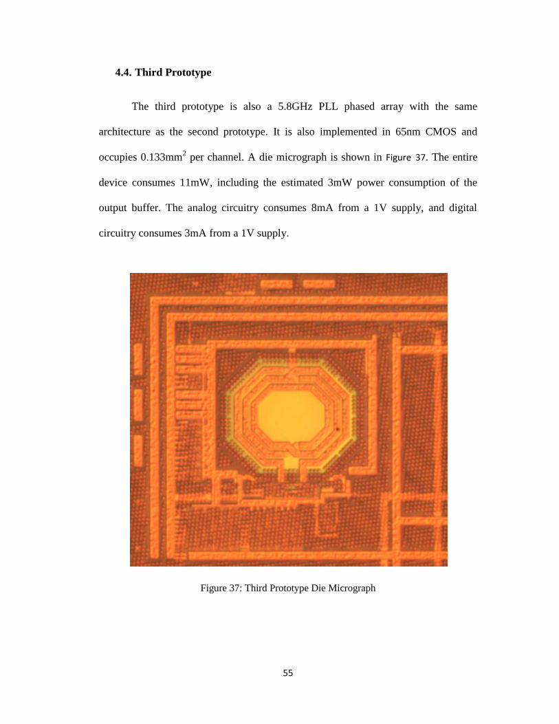
4.4. Third Prototype
The third prototype is also a 5.8GHz PLL phased array with the same
architecture as the second prototype. It is also implemented in 65nm CMOS and
occupies 0.133mm2 per channel. A die micrograph is shown in Figure 37. The entire
device consumes 11mW, including the estimated 3mW power consumption of the
output buffer. The analog circuitry consumes 8mA from a 1V supply, and digital
circuitry consumes 3mA from a 1V supply.
Figure 37: Third Prototype Die Micrograph
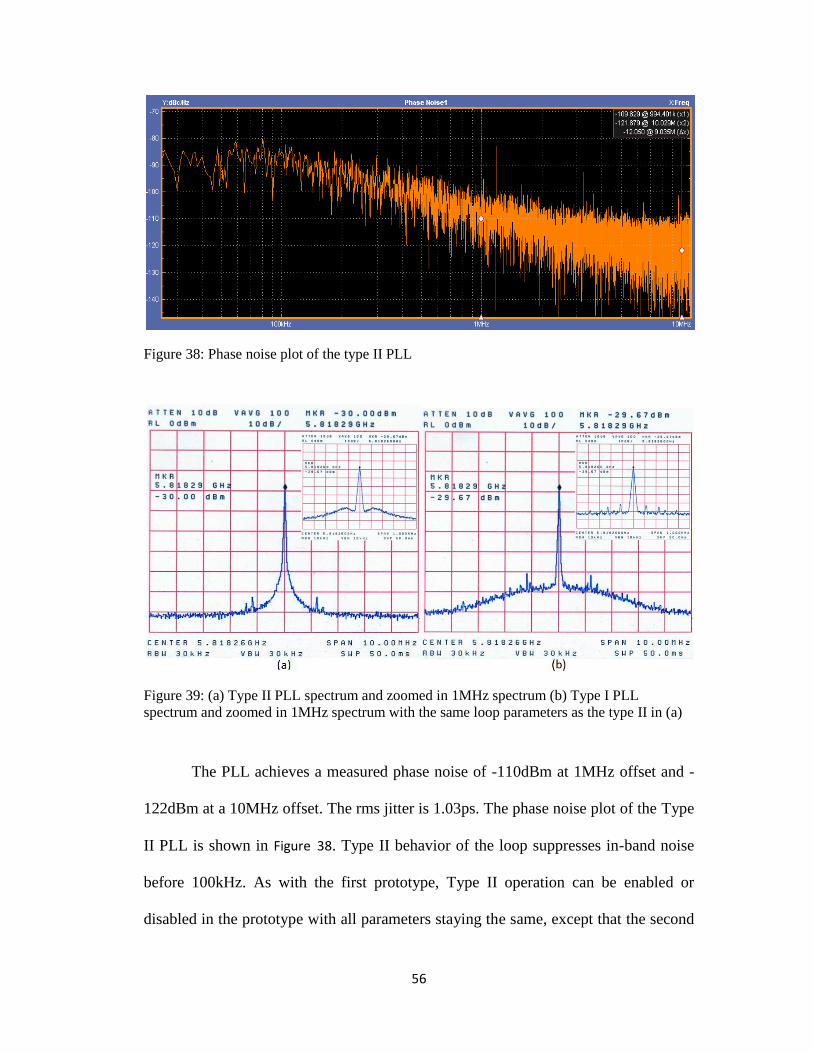
56
Figure 38: Phase noise plot of the type II PLL
Figure 39: (a) Type II PLL spectrum and zoomed in 1MHz spectrum (b) Type I PLL
spectrum and zoomed in 1MHz spectrum with the same loop parameters as the type II in (a)
The PLL achieves a measured phase noise of -110dBm at 1MHz offset and -
122dBm at a 10MHz offset. The rms jitter is 1.03ps. The phase noise plot of the Type
II PLL is shown in Figure 38. Type II behavior of the loop suppresses in-band noise
before 100kHz. As with the first prototype, Type II operation can be enabled or
disabled in the prototype with all parameters staying the same, except that the second
57
integrator is turned off in Type I mode. Measured spectrum profiles for Type I and
Type II modes are compared in Figure 39. As expected, the Type II mode suppresses
in-band noise much better than Type I.
Figure 40: Phase shift vs. digital input
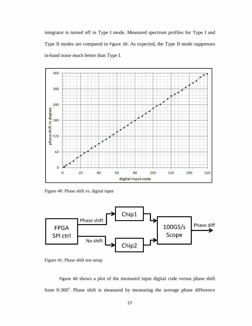
Figure 41: Phase shift test setup
Figure 40 shows a plot of the measured input digital code versus phase shift
from 0-360o. Phase shift is measured by measuring the average phase difference
58
between two phase-setting PLLs, with one generating a fixed phase to serve as a
measurement reference shown in Figure 41. An average phase shift of 2.25o or 7.3bits
of phase resolution and a phase range of more than 720o are achieved. The maximum
phase shift is limited by the size of the internal digital buffers, and the minimal phase
shift is limited by phase noise. A phase shift of 90o settles to within 3
o accuracy
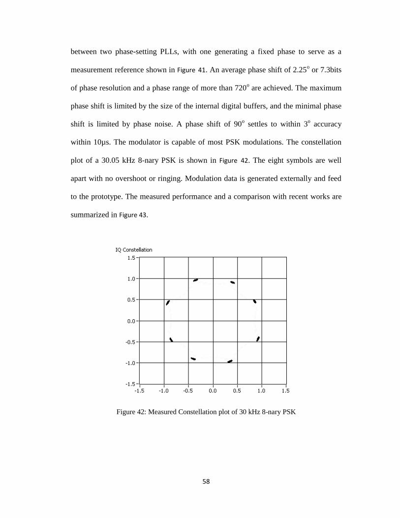
within 10µs. The modulator is capable of most PSK modulations. The constellation
plot of a 30.05 kHz 8-nary PSK is shown in Figure 42. The eight symbols are well
apart with no overshoot or ringing. Modulation data is generated externally and feed
to the prototype. The measured performance and a comparison with recent works are
summarized in Figure 43.
Figure 42: Measured Constellation plot of 30 kHz 8-nary PSK
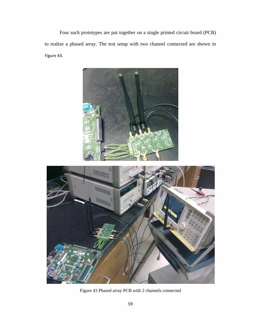
59
Four such prototypes are put together on a single printed circuit board (PCB)
to realize a phased array. The test setup with two channel connected are shown in
Figure 43.
Figure 43 Phased array PCB with 2 channels connected
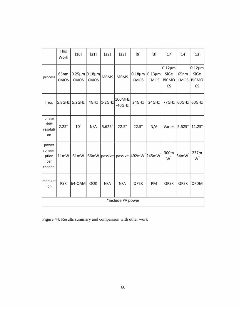
60
This
Work [16] [31] [32] [33] [9] [3] [17] [14] [13]
process 65nm
CMOS
0.25μm
CMOS
0.18μm
CMOS MEMS MEMS
0.18μm
CMOS
0.13μm
CMOS
0.12μm
SiGe
BiCMO
CS
65nm
CMOS
0.12μm
SiGe
BiCMO
CS
freq. 5.8GHz 5.2GHz 4GHz 1-2GHz 100MHz
-40GHz 24GHz 24GHz 77GHz 60GHz 60GHz
phase
shift
resoluti
on
2.25o 10o N/A 5.625o 22.5o 22.5o N/A Varies 5.625o 11.25o
power
consum
ption
per
channel
11mW 61mW 66mW passive passive 492mW* 245mW* 300m
W* 34mW*
237m
W*
modulat
ion PSK 64-QAM OOK N/A N/A QPSK PM QPSK QPSK OFDM
*include PA power
Figure 44: Results summary and comparison with other work
61
Chapter 5
Conclusion
5.1. Key contributions
The primary contribution of this work is the development and demonstration
of a novel CMOS phased array architecture using phase-setting PLLs. Various
conventional CMOS phased array architectures are either CMOS incompatible due to
component size or have output phase resolution or linearity limitations. This work
overcomes these shortcomings.
Compared to existing phased array architectures discussed in section 1.3 and
1.4, this architecture has many advantages. This architecture does not require low loss
phase shifters at RF frequencies, which are difficult to build. The output before the
PA is an un-attenuated full-scale signal. Also it does not require any large phase
shifters that are hard to integrate onto CMOS.
Compared to the popular phase rotator architecture discussed in section 1.4.3,
this architecture retains most of its benefits while improves on some of its
shortcomings. First of all, the most important advantage of this architecture is that it
can achieve a very linear and high resolution phase shift. The output phase vs. input
62
digital code linearity is outstanding. The phase resolution is only limited by the PLL’s
phase noise. The prototype achieves the highest phase resolution reported. Although
in a phased array system with few elements, this resolution would not be fully
utilized. In a large array with high number of elements, high phase resolution could
translate to very fine radiation angle. Secondly this architecture does not require
complicated high frequency LO distribution network. Although you still need to
distribute the reference clock signal to all PLLs, it’s at a much lower frequency than
the output RF frequency. Nothing special need to done to ensure its proper
distribution. And finally this architecture does not require quadrature I/Q signals.
In addition, this work improves on previous digital PLL design to achieve
Type II behavior with a 1-bit TDC PLL architecture. This improvement allows this
popular architecture to suppress in-band noise and reduces overall jitter. In doing so,
we demonstrate that one of this digital PLL architecture’s shortcomings can be
overcome.
63
5.2. Future works
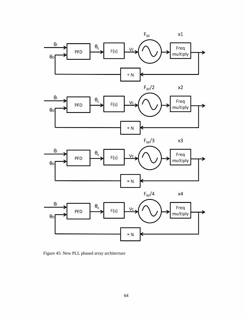
One difficulty encountered in this work is the problem of on chip inductor
coupling. Since inductor coupling is stronger as their resonance frequency get closer,
inductors used in PLLs experience the worst case scenario. To overcome this issue,
one of the solutions is to use VCOs with different frequencies in each channel shown
in Figure 45. Each VCO in the original design is replaced with a real VCO and a
frequency multiplier. The combined output of the two blocks is still at the original RF
frequency. But each VCO has a different oscillating frequency and thus does not
couple to the other VCOs. A low noise frequency multiplier is a challenge in this
architecture.
64
Figure 45: New PLL phased array architecture
65
Another more fundamental solution to overcome on-chip inductor coupling is
to switch from LC VCOs to ring oscillators. With new development in the area of
noise cancelling oscillators [34], the traditional phase noise limitation that restricts
transmitters from using anything besides LC VCOs will be gone. This will not only
solve the problem of inductor coupling, it can significantly reduce the area of a PLL.
Such development can lead to very compact individual channel PLLs and thus large
number of element arrays. With large number of elements, this PLL phased array
architecture’s high phase resolution can be fully utilized.
66
Appendix A
A flexible wireless receiver with configurable DT filter
embedded in a SAR ADC
The following section discusses the other work [35] completed in
collaboration with David Lin.
A.1 Introduction
The modern day desire for ubiquitous connectivity using multiple standards
and bands necessitates the development of flexible, software-configurable receivers.
One of the challenges of creating such receivers is the design of low power,
configurable filters for rejecting aliasing interferers and adjacent channels. Analog
filters become difficult to design at the reduced supply voltages of deep submicron
processes. Digital filters require significant over-sampling with a high resolution
ADC, at the expense of power consumption, in order to prevent aliasing of the
interferer and to capture a weak wanted signal in the presence of a strong interferer.
This work presents a better alternative of embedding a software-configurable,
discrete time (DT) filter within a SAR ADC. The DT filter attenuates interference by
performing passive charge-sharing, so power consumption and speed improve with
process scaling. Compared to receivers with a separate DT filter stage [36][37], the
embedded filter reduces capacitor area and saves energy by eliminating charge
67
resampling between the filter and the ADC [38]. Configurability allows the receiver
to adapt to its environment and to different communication standards. For example,
the receiver can save power by operating in a “no filter” mode when no interferer or
adjacent channel activity is present. As the power and the frequency of the interferer
change, the receiver can respond by enabling the DT filter and optimally adjusting
sampling rate and filter parameters. This 500MHz to 3.6GHz configurable receiver is
verified with the 915MHz and 2450MHz bands of the IEEE 802.15.4 standard and
the IEEE 802.11 standard.
A.2 Receiver Architecture
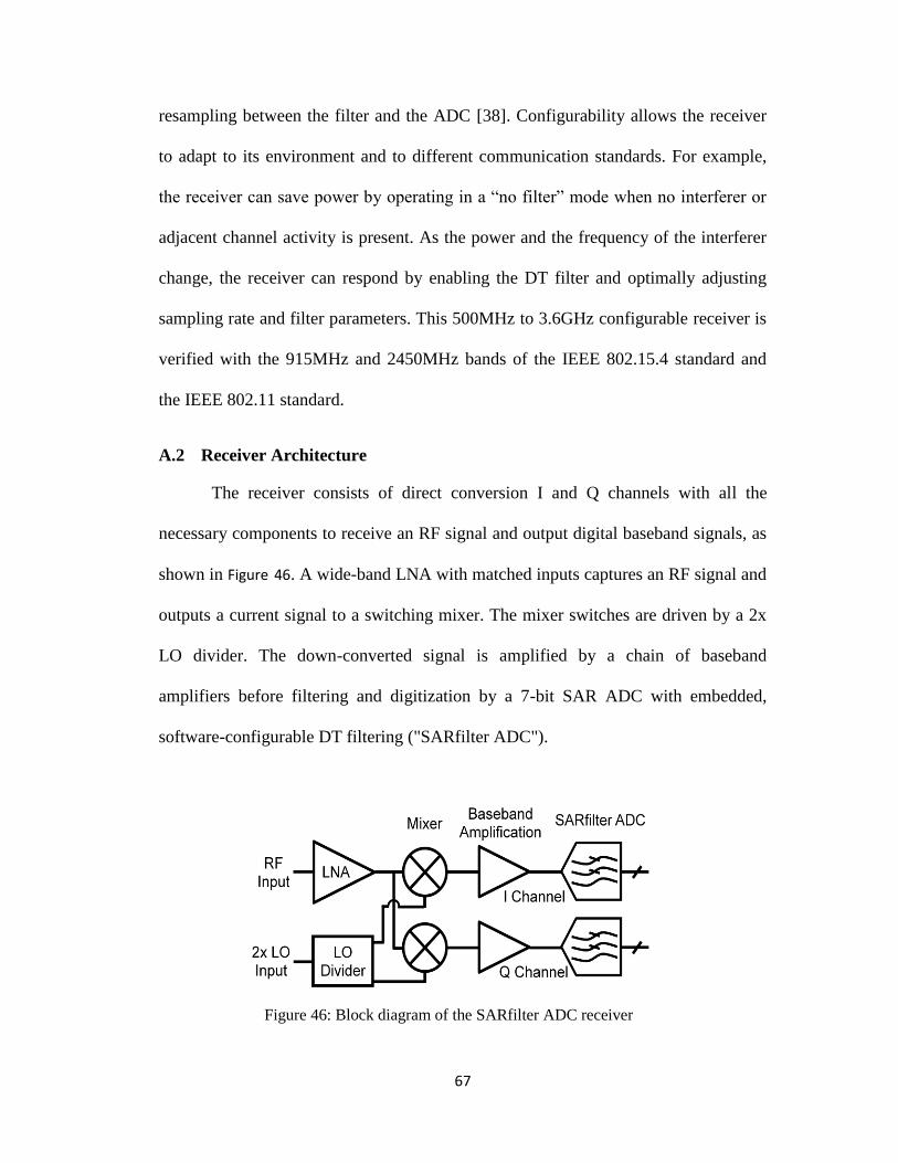
The receiver consists of direct conversion I and Q channels with all the
necessary components to receive an RF signal and output digital baseband signals, as
shown in Figure 46. A wide-band LNA with matched inputs captures an RF signal and
outputs a current signal to a switching mixer. The mixer switches are driven by a 2x
LO divider. The down-converted signal is amplified by a chain of baseband
amplifiers before filtering and digitization by a 7-bit SAR ADC with embedded,
software-configurable DT filtering ("SARfilter ADC").
Figure 46: Block diagram of the SARfilter ADC receiver
68
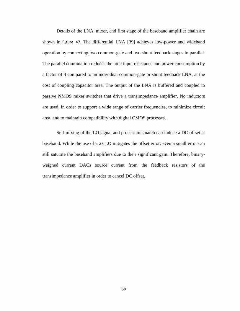
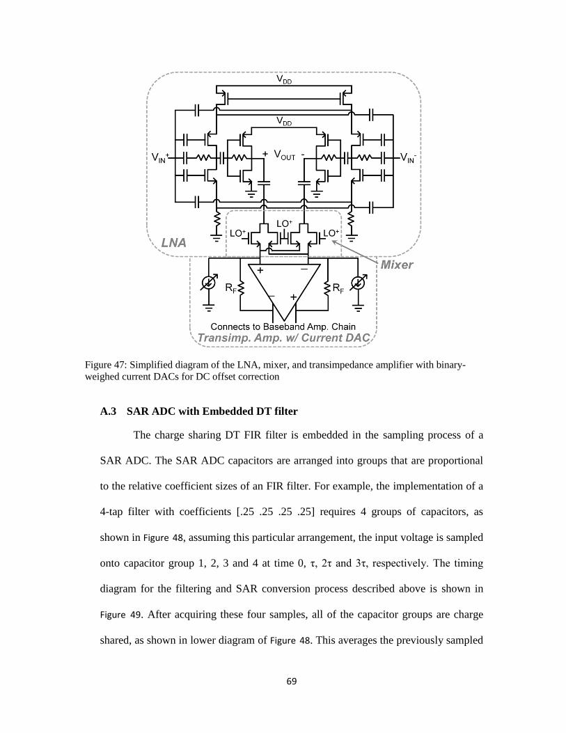
Details of the LNA, mixer, and first stage of the baseband amplifier chain are
shown in Figure 47. The differential LNA [39] achieves low-power and wideband
operation by connecting two common-gate and two shunt feedback stages in parallel.
The parallel combination reduces the total input resistance and power consumption by
a factor of 4 compared to an individual common-gate or shunt feedback LNA, at the
cost of coupling capacitor area. The output of the LNA is buffered and coupled to
passive NMOS mixer switches that drive a transimpedance amplifier. No inductors
are used, in order to support a wide range of carrier frequencies, to minimize circuit
area, and to maintain compatibility with digital CMOS processes.
Self-mixing of the LO signal and process mismatch can induce a DC offset at
baseband. While the use of a 2x LO mitigates the offset error, even a small error can
still saturate the baseband amplifiers due to their significant gain. Therefore, binary-
weighed current DACs source current from the feedback resistors of the
transimpedance amplifier in order to cancel DC offset.
69
A.3 SAR ADC with Embedded DT filter
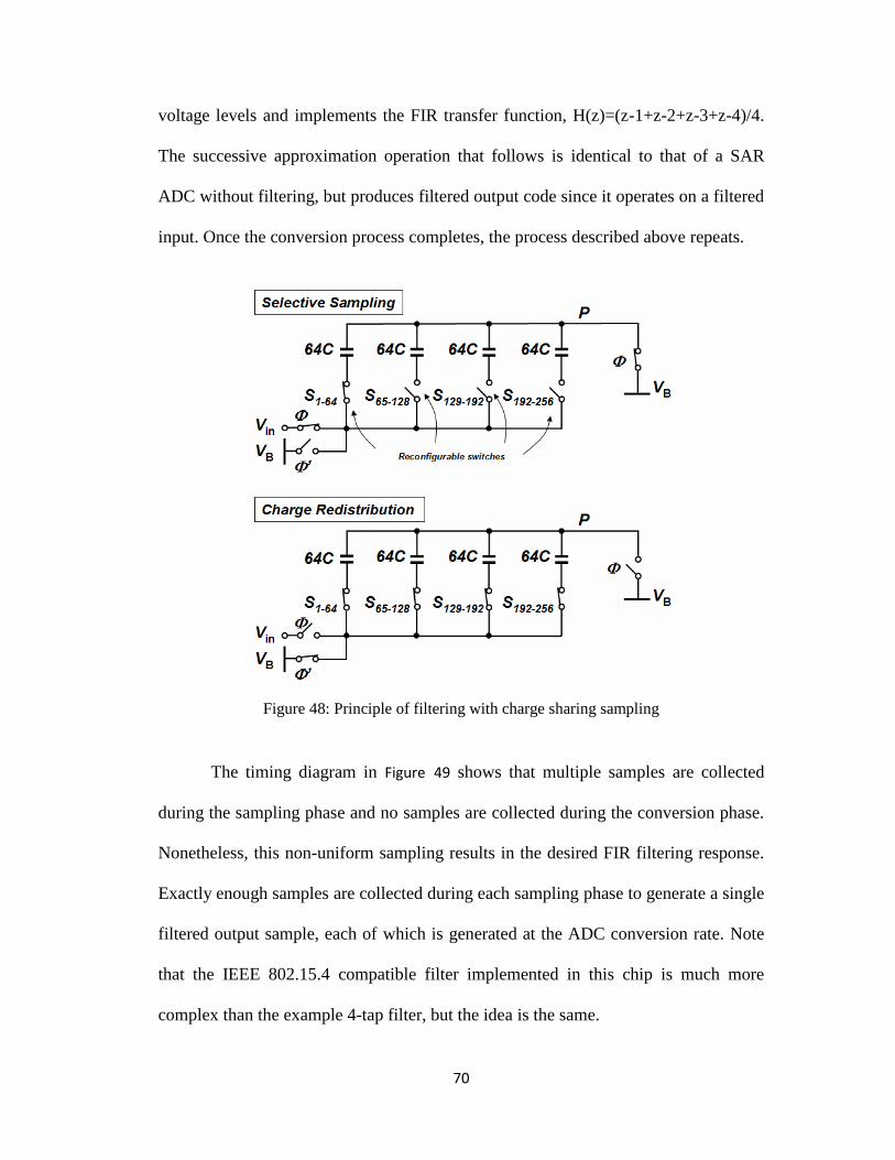
The charge sharing DT FIR filter is embedded in the sampling process of a
SAR ADC. The SAR ADC capacitors are arranged into groups that are proportional
to the relative coefficient sizes of an FIR filter. For example, the implementation of a
4-tap filter with coefficients [.25 .25 .25 .25] requires 4 groups of capacitors, as
shown in Figure 48, assuming this particular arrangement, the input voltage is sampled
onto capacitor group 1, 2, 3 and 4 at time 0, τ, 2τ and 3τ, respectively. The timing
diagram for the filtering and SAR conversion process described above is shown in
Figure 49. After acquiring these four samples, all of the capacitor groups are charge
shared, as shown in lower diagram of Figure 48. This averages the previously sampled
Figure 47: Simplified diagram of the LNA, mixer, and transimpedance amplifier with binary-
weighed current DACs for DC offset correction
70
voltage levels and implements the FIR transfer function, H(z)=(z-1+z-2+z-3+z-4)/4.
The successive approximation operation that follows is identical to that of a SAR
ADC without filtering, but produces filtered output code since it operates on a filtered
input. Once the conversion process completes, the process described above repeats.
Figure 48: Principle of filtering with charge sharing sampling
The timing diagram in Figure 49 shows that multiple samples are collected
during the sampling phase and no samples are collected during the conversion phase.
Nonetheless, this non-uniform sampling results in the desired FIR filtering response.
Exactly enough samples are collected during each sampling phase to generate a single
filtered output sample, each of which is generated at the ADC conversion rate. Note
that the IEEE 802.15.4 compatible filter implemented in this chip is much more
complex than the example 4-tap filter, but the idea is the same.
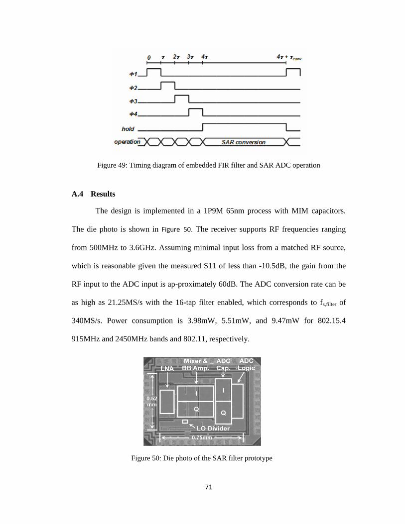
71
Figure 49: Timing diagram of embedded FIR filter and SAR ADC operation
A.4 Results
The design is implemented in a 1P9M 65nm process with MIM capacitors.
The die photo is shown in Figure 50. The receiver supports RF frequencies ranging
from 500MHz to 3.6GHz. Assuming minimal input loss from a matched RF source,
which is reasonable given the measured S11 of less than -10.5dB, the gain from the
RF input to the ADC input is ap-proximately 60dB. The ADC conversion rate can be
as high as 21.25MS/s with the 16-tap filter enabled, which corresponds to fs,filter of
340MS/s. Power consumption is 3.98mW, 5.51mW, and 9.47mW for 802.15.4
915MHz and 2450MHz bands and 802.11, respectively.
Figure 50: Die photo of the SAR filter prototype
72
Reference
[1] G. E. Moore, "Cramming more components onto integrated circuits,"
Electronics, vol. 38, no. 8, p. 114–117, Apr. 1965..
[2] M. Perrott, Techniques for High Data Rate Modulation and Low Power
Operation of Fractional-N Frequency Synthesizer, Cambridge, MA: Ph.D.
dissertation MIT, 1997.
[3] H. Krishnaswamy and H. Hashemi, "A Fully Integrated 24 GHz 4-Channel Phased
Array Trasnceiver in 0.13μm CMOS Based on a Variable-Phase Ring Oscillator
and PLL Architecture," in ISSCC Dig. Tech., 2007.
[4] M. Ferriss, D. Lin and M. P. Flynn, "A Fractional-N PLL modulator with flexible
direct digital phase modulation," in IEEE Custom Integrated Circuits Conf., 2009.
[5] R. B. Staszewski, J. L. Wallberg, S. Rezeq, C. M. Hung, O. E. Eliezer, S. K.
Verrulapalli, C. Fernando, K. Maggio, R. Staszewski, N. Barton, M. C. Lee, P.
Cruise, M. Entezari, K. Muhammed and D. Leipold, "All-digital PLL and
transmitter for mobile phones," IEEE J. Solid-State Circuits, vol. 40, no. 12, p.
2469–2482, 2005.
[6] M. Ferriss and M. P. Flynn, "A 14mW Fractional-N PLL modulator with an
enhanced digital phase detector and frequency switching scheme," in IEEE ISSCC
Tech. Dig., 2007.
[7] Y. Elboim, A. Kolodny and R. Ginosar, "A Clock-Tuning Circuit for System-on-
Chip," IEEE trans. on VLSI, vol. 11, no. 4, pp. 616 - 626, 2003.
[8] J. Park, J. Kang, S. Park and M. P. Flynn, "A 9Gbit/s Serial Transceiver for On-chip
Global Signaling over Lossy Transmission Lines," in IEEE Custom Intergrated
Circuits Conf. (CICC), 2008.
73
[9] A. Hajimiri, H. Hashemi, A. Natarajan, X. Guan and A. Komijani, "Integrated
phased array systems in silicon," proceeding of the IEEE, vol. 93, no. 9, pp. 1637 -
1655, 2005.
[10] D. Parker and D. C. Zimmermann, "Phased Arrays—Part I: Theory and
Architectures," IEEE Trans. Microw. Theory Tech., vol. 50, no. 3, pp. 678-687,
2002.
[11] D. Parker and D. Zimmermann, "Phased-arrays—Part II: Implementations,
applications, and future trends," IEEE Trans. Microw. Theory Tech. , vol. 50, no.
3, pp. 688-698, 2002.
[12] H. Zarei and D. Allstot, "A low-loss phase shifter in 180 nm CMOS for multiple-
antenna receivers," in IEEE ISSCC Tech. Dig. , 2004.
[13] A. Valdes-Garcia, S. T. Nicolson, J. Lai, A. Natarajan, P. Chen, S. K. Reynolds, J.
Zhan, D. Kam, D. Liu and B. Floyd, "A Fully-Integrated 16-Element Phased-Array
Transmitter in SiGe BiCMOS for 60-GHz Communications," IEEE JSSC, vol. 45, no.
12, pp. 2757 - 2773, 2010.
[14] M. Tabesh, J. Chen, C. Marcu, L. Kong, S. Kang, A. M. Niknejad and E. Alon, "A 65
nm CMOS 4-Element Sub-34 mW/Element 60 GHz Phased-Array Transceiver,"
IEEE JSSC, vol. 46, no. 12, pp. 3018-3032, 2011.
[15] H. Hashemi, X. Guan, A. Komijani and A. Hajimiri, "A 24-GHz SiGe Phased-Array
Receiver—LO Phase-Shifting Approach," IEEE Trans. Microw. Theory Tech., vol.
53, no. 2, pp. 614-626, 2005.
[16] S. Gueorguiev, S. Lindfors and T. Larsen, "A 5.2 GHz CMOS I/Q Modulator With
Integrated Phase Shifter for Beamforming," IEEE JSSC, vol. 42, no. 9, pp. 1953-
1962, 2007.
[17] A. Natarajan, A. Komijani, X. Guan, A. Babakhani and A. Hajimiri, "A 77-GHz
Phased-Array Transceiver With On-Chip Antennas in Silicon: Transmitter and
Local LO-Path Phase Shifting," IEEE JSSC, vol. 41, no. 12, pp. 2807-2819, 2006.
[18] F. Ellinger, H. Jäckel and W. Bächtold, "Varactor-loaded transmission-line phase
shifter at C-band using lumped elements," IEEE Trans. Microwave Theory Tech.,
vol. 51, no. 4, pp. 1135-1140, 2003.
74
[19] C. F. Campbell and S. A. Brown, "A compact 5-bit phase-shifter MMIC for K-band
satellite communication systems," IEEE Trans. on Microwave Theory and
Techniques (MTT), vol. 48, no. 12, pp. 2652-2656, 2000.
[20] M. Chua and K. Martin, "1GHz Programmable Analog Phase Shifter for adaptive
antennas," in Custom Integrated Circuits Conference (CICC), 1998.
[21] K. Koh and G. M. Rebeiz, "0.13-um CMOS Phase Shifters for X-, Ku-, and K-Band
Phased Arrays," IEEE JSSC, vol. 42, no. 11, pp. 2535-2546, 2007.
[22] F. M. Gardner, Phase-Lock Techniques, New York: Wiley, 1966.
[23] P. Gray, P. Hurst, S. Lewis and R. Meyer, "10.4 Phase-Locked Loop (PLL)," in
Analysis and Design of Analog Integrated Circuits, Wiley, 2001, p. 720.
[24] I. A. Young, J. Greason and K. Wong, "A PLL Clock Generator with 5 to 110 MHz
of Lock Range for Microprocessors," IEEE JSSC, vol. 27, no. 11, pp. 1599-1607,
1992.
[25] P. Hanumolu, M. Brownlee, K. Mayaram and U. Moon, "Analysis of Charge-
Pump Phase-Locked Loops," IEEE Trans. on Circuits and Systems I (TCAS I), vol.
51, no. 9, pp. 1665-1674, 2004.
[26] W. Rhee, "Design of high-performance CMOS charge pumps in phase-locked
loops," in IEEE International Symposium on Circuits and Systems (ISCAS), 1999.
[27] Y. Zhang, W. Wu, G. Yang and J. Zhao, "DDS-PLL Phased Source for Beam Control
Active Phased Array," in Asia-Pacific Microwave Conference (APMC), 2008.
[28] A. Oppenheim, Discrete Time Signal Processing Third Edition, Upper Saddle
River, NJ: Pearson Higher Education, Inc, 2010.
[29] C. Y. Lau and M. H. Perrott, "Fractional-N frequency synthesizer design at the
transfer function level using a direct closed loop realization algorithm," in Proc.
Design Automation Conference, 2003.
[30] B. Razavi, "The Role of PLLs in Future Wireline Transmitters," IEEE Trans. Circuits
and Systems I: Regular Papers, vol. 56, no. 8, pp. 1786-1793, 2009.
[31] S. Diao, Y. Zheng, Y. Gao, X. Yuan and C. Heng, "3–5GHz IR-UWB timed array
75
transmitter in 0.18μm CMOS," in A-SSCC, 2009.
[32] J. Reinke, L. Wang, G. K. Fedder and T. Mukherjee, "A 4-bit RF MEMS phase
shifter monolithically integrated with conventional CMOS," in IEEE 24th
International Conference on Micro Electro Mechanical Systems (MEMS), 2011.
[33] J. Lampen, S. Majumder, C. Ji and J. Maciel, "Low-loss, MEMS based, broadband
bhase shifters," in IEEE International Symposium on Phased Array Systems and
Technology (ARRAY), 2010.
[34] A. Sai, T. Yamaji and T. Itakura, "A 570fsrms integrated-jitter ring-VCO-based
1.21GHz PLL with hybrid loop," in IEEE ISSCC Dig. Tech., 2011.
[35] D. T. Lin, L. Li, S. Farahani and M. P. Flynn, "A Flexible 500MHz to 3.6GHz
Wireless Receiver with Configurable DT FIR and IIR Filter Embedded in a 7b
21MS/s SAR ADC," in IEEE Custom Integrated Circuits Conf. (CICC), 2010.
[36] K. Muhammad, Y. Mayhugh, C. Hung, T. Jung and I. Elahi, "A Discrete Time
Quad-band GSM/GPRS Receiver in a 90nm Digital CMOS Process," IEEE Custom
Integrated Circuit Conf., pp. 809-812, 2005.
[37] R. Bagheri, A. Mirzaei, S. Chehrazi, M. Heidari, M. Lee and M. Mikhemar, "An
800-MHz–6-GHz Software-Defined Wireless Receiver in 90-nm CMOS," IEEE
JSSC, vol. 41, no. 12, pp. 2860-2876, 2006.
[38] J. Kang, D. Lin, L. Li and M. P. Flynn, "A Reconfigurable FIR Filter Embedded in a
9b Successive Approximation ADC," in IEEE Custom Integrated Circuits Conf.,
2008.
[39] S. Wang, A. Niknejad and R. Brodersen, "Design of a Sub-mW 960-MHz UWB
CMOS LNA," IEEE JSSC, vol. 41, no. 11, pp. 2449-2456, 2006.


![Design of a Non-PLL Grid-Forming Inverter for Smooth ...inverter controller designs [2][6][11], leverages a phased-lock loop (PLL), which makes the GFM inverter susceptible to injecting](https://img.pdfslide.net/doc/110x75/60fb0aa2a2d1922972547220/design-of-a-non-pll-grid-forming-inverter-for-smooth-inverter-controller-designs.jpg)