Embed Size (px)
Citation preview

ORG447X Series Datasheet
Fully Integrated GPS Modules
Document number: 010311 For technical questions contact: [email protected] www.origingps.com Revision: B00 01-03-11
- 1 -
Fully Integrated GPS Receiver
Engine Module
ORG447X Series Data Sheet
All trademarks are properties of their respective owners. Performance characteristics listed in this document do not constitute a warranty or guarantee of product performance. OriginGPS assumes no liability or responsibility for any claims or damages arising out of the use of this document, or from the use of integrated circuits based on this document. OriginGPS reserves the right to make changes in its products, specifications and other information at any time without notice. OriginGPS navigation products are not recommended to use in life saving or life sustaining applications.

ORG447X Series Datasheet
Fully Integrated GPS Modules
Document number: 010311 For technical questions contact: [email protected] www.origingps.com Revision: B00 01-03-11
- 2 -
1. Introduction
The ORG447X series module is industry’s smallest, autonomous, fully featured GPS engine.
The ORG447X series module is miniature multi-channel receiver that continuously tracks all satellites in view and provides accurate positioning data in industry’s standard NMEA format.
Internal ARM CPU core and sophisticated firmware keep GPS payload off the host and allow integration in low resources embedded solutions.
Featuring OriginGPS proprietary Noise-Free Zone System (NFZ™) technology the ORG447X offers the ultimate in high sensitivity GPS performance in small size.
The ORG447XX series module is complete SiP (System-in-Package) featuring advanced miniature packaging technology and an ultra small footprint designed to commit unique integration features for high volume, low power and cost sensitive applications.
The ORG447X module incorporates new SiRFstarIV™ GPS processor.
The revolutionary SiRFstarIV™ architecture is optimized for how people really use location-aware products: often indoors with periods of unobstructed sky view when moving from place to place.
This new architecture can detect changes in context, temperature, and satellite signals to achieve a state of near continuous availability by maintaining and opportunistically updating its internal fine time, frequency, and satellite Ephemeris data while consuming mere microwatts of battery power.

ORG447X Series Datasheet
Fully Integrated GPS Modules
Document number: 010311 For technical questions contact: [email protected] www.origingps.com Revision: B00 01-03-11
- 3 -
2. Description
OriginGPS has researched and enhanced the performance of standard GPS receivers in real-life applications. Case study of the specifications of key components through involvement in R&D effort of major vendors derived in highest performance in industry’s smallest footprint parts available. These carefully selected key components resulted in higher sensitivity, faster position fix, navigation stability and operation robustness under rapid environmental changes creating hard-to-achieve laboratory performance in heavy-duty environment.
2.1. Features
Stand alone operation OriginGPS Noise Free Zone System (NFZ™) technology Integrated LNA, SAW Filter, TCXO and RTC SiRFstarIV™ GSD4e GPS processor L1 frequency, C/A code 48 track verification channels Navigation sensitivity: -160dBm Tracking sensitivity: -163dBm for indoor fixes
Fast TTFF:
Multipath mitigation and indoor tracking Active Jammer Remover: tracks up to 8 CW interferers and removes jammers up to 80dB-Hz SBAS (WAAS, EGNOS, MSAS) support1 Almanac Based Positioning (ABP™)1 Client Generated Extended Ephemeris (CGEE™) and Server Generated Extended Ephemeris
(SGEE™) for very fast TTFFs are supported through SiRFInstantFix™ and SiRFInstantFixII™ Assisted GPS (A-GPS) support Automatic and user programmable power saving scenarios: ATP™, PTF™, APM™ SiRFAware™ Micro Power Mode (MPM™) support1 Low power consumption: <10mW during ATP™ ARM7® 109MHz baseband CPU Smart sensor I2C master interface1 Selectable UART, SPI or I2C host interface Programmable communication protocol and message rate Selectable NMEA or OSP (SiRF Binary) communication standards Single voltage supply: 1.8V DC blocked 50Ω antenna input Ultra small footprint: 7mm x 7mm Surface Mount Device (SMD) Optimized for automatic assembly and reflow equipment Industrial operating temperature range: -400 to 850C Pb-Free RoHS compliant
Note: 1. Not available in modules with Standard firmware
< 35s under Cold Start conditions
< 1s under Hot Start conditions

ORG447X Series Datasheet
Fully Integrated GPS Modules
Document number: 010311 For technical questions contact: [email protected] www.origingps.com Revision: B00 01-03-11
- 4 -
2.2. Architecture
1PPS
BB Power
RF Power
UART
RTC
TCXO
Power
Management
POR
SPI
LNA
GPS
Search / Track
Correlator
Engine
Sample
RAM
Embedded
Processor
Subsystem
ROM / RAM
I/O
bu
ffe
rs
VCC 1.8V
GSD4e
SAW Filter
I2C
DR I2C
ORG447X
ON OFF
HOST
WAKEUP
Serial Flash /
E2PROM
Gyroscope
(option)
Accelerometer
(option)
(option)
GPS
Antenna
Figure 2-1: ORG447X architecture
Band-pass SAW filter
Band-pass SAW filter eliminates inter-modulated out-of-band signals that may corrupt GPS receiver performance.
LNA (Low Noise Amplifier)
The integrated LNA amplifies the GPS signal to meet RF down converter input threshold. Noise figure optimized design was implemented to provide maximum sensitivity.
TCXO (Temperature Compensated Crystal Oscillator)
This highly stable 16.369 MHz oscillator controls the down conversion process in RF block. Highest characteristics of this component are key factors in fast TTFF.
RTC (Real Time Clock) crystal
This miniature component with very tight specifications is necessary for maintaining Hot start and Warm start capabilities.
RF shield
RF enclosure avoids external interference to compromise sensitive circuitry inside the receiver. RF shield is also blocks module’s internal emissions from being transmitted.

ORG447X Series Datasheet
Fully Integrated GPS Modules
Document number: 010311 For technical questions contact: [email protected] www.origingps.com Revision: B00 01-03-11
- 5 -
GSD4e IC
Figure 2-2: GSD4e functional block diagram
SiRFstarIV™ GSD4e GPS processor includes the following units:
GPS RF core incorporating LNA, down converter, fractional-N synthesizer and ADC block with selectable 2 and 4-bit quantization
GPS DSP core incorporating more than twice the clock speed and more than double the RAM capacity relative to predecessor - market benchmarking SiRFStarIII™ DSP core
ARM7® microprocessor system incorporating 109MHz CPU and interrupt controller
ROM block as code storage for PVT applications
RAM block for data cache
RTC block
UART block
SPI block
I2C block
Power control block for internal voltage domains management

ORG447X Series Datasheet
Fully Integrated GPS Modules
Document number: 010311 For technical questions contact: [email protected] www.origingps.com Revision: B00 01-03-11
- 6 -
2.3. Applications
ORG447X series GPS receiver modules have been designed to address new markets where ultra small size and high performance does commit to traditional GPS modules demand for standalone operation, high level of integration, power consumption and design flexibility.
ORG4472
The ORG4472 is standard version of the ORG447X series GPS antenna modules.
The ORG4472 is ideal for standard positioning and navigation applications including indoor tracking: Personal locators Pet collars People and animal tracking systems Asset tracking SKU systems Sports and recreation accessories Handheld consumer navigation and multifunction devices Rescue and emergency systems Precise timing devices Micro robots and micro UAVs Automatic Vehicle Location Automotive navigation Workforce management Railway monitoring GIS and mapping Civil engineering Agriculture automation Maritime navigation Electronic Toll Collection Automotive security systems Data loggers Weather balloons WiMAX base stations, Femto and Pico cells Industrial sensor platforms Location Based Services Scientific applications
ORG4471
The ORG4471 is ideal for highly embedded portable electronics applications with height limitations. Mobile handsets GPS watches Digital still cameras Mobile game consoles Homeland security applications

ORG447X Series Datasheet
Fully Integrated GPS Modules
Document number: 010311 For technical questions contact: [email protected] www.origingps.com Revision: B00 01-03-11
- 7 -
3. Electrical Specifications
3.1. Absolute Maximum Ratings
Absolute Maximum Ratings are stress ratings only.
Stresses exceeding Absolute Maximum Ratings may damage the device.
Parameter Symbol Min Max Units
Power Supply Voltage VCC - 2.2 V
RF Input Voltage VRF_IN -50 50 V
Power Dissipation PD - 200 mW
I/O Voltage VIO -0.3 3.6 V
I/O Source/Sink Current IIO -10 +10 mA
RF Input Power fIN = 1560MHz÷1590MHz
PRF_IN
- 10 dBm
fIN <1560MHz, >1590MHz - +15 dBm
ESD Rating I/O pads VIO(ESD) -2 +2 kV
RF input pad VRF(ESD) -1 +1 kV
Storage temperature TST -55 +125 0C
Lead temperature (10 sec. @ 1mm from case) TLEAD - +260 0C
Table 3-1: Absolute maximum ratings
ORG447X Series Datasheet
Fully Integrated GPS Modules
Document number: 010311 For technical questions contact: [email protected] www.origingps.com Revision: B00 01-03-11
- 8 -
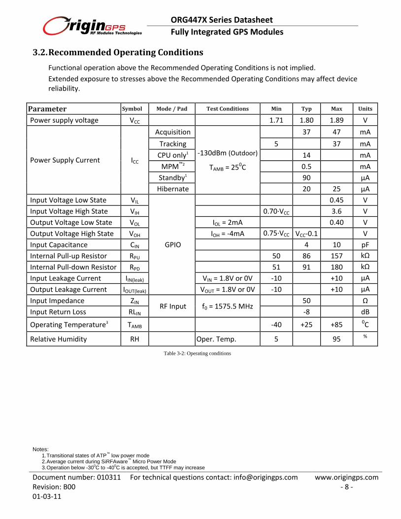
3.2. Recommended Operating Conditions
Functional operation above the Recommended Operating Conditions is not implied.
Extended exposure to stresses above the Recommended Operating Conditions may affect device reliability.
Parameter Symbol Mode / Pad Test Conditions Min Typ Max Units
Power supply voltage VCC 1.71 1.80 1.89 V
Power Supply Current ICC
Acquisition
-130dBm (Outdoor)
TAMB = 250C
37 47 mA
Tracking 5 37 mA
CPU only1 14 mA
MPM™2 0.5 mA
Standby1 90 µA
Hibernate 20 25 µA
Input Voltage Low State VIL
GPIO
0.45 V
Input Voltage High State VIH 0.70·VCC 3.6 V
Output Voltage Low State VOL IOL = 2mA 0.40 V
Output Voltage High State VOH IOH = -4mA 0.75·VCC 0.1
VCC-0.1 V
Input Capacitance CIN 4 10 pF
Internal Pull-up Resistor RPU 50 86 157 kΩ
Internal Pull-down Resistor RPD 51 91 180 kΩ
Input Leakage Current IIN(leak) VIN = 1.8V or 0V -10 +10 µA
Output Leakage Current IOUT(leak) VOUT = 1.8V or 0V -10 +10 µA
Input Impedance ZIN RF Input f0 = 1575.5 MHz
50 Ω
Input Return Loss RLIN -8 dB
Operating Temperature3 TAMB -40 +25 +85 0C
Relative Humidity RH Oper. Temp. 5 95 %
Table 3-2: Operating conditions
Notes:
1. Transitional states of ATP™
low power mode 2. Average current during SiRFAware
™ Micro Power Mode
3. Operation below -300C to -40
0C is accepted, but TTFF may increase

ORG447X Series Datasheet
Fully Integrated GPS Modules
Document number: 010311 For technical questions contact: [email protected] www.origingps.com Revision: B00 01-03-11
- 9 -
4. Performance
4.1. Acquisition Times
TTFF (Time To First Fix) – is the period of time from GPS power-up till position estimation.
Hot Start
A hot start results from software reset after a period of continuous navigation or a return from a short idle period that was preceded by a period of continuous navigation. In this state, all of the critical data (position, velocity, time, and satellite ephemeris) is valid to the specified accuracy and available in SRAM.
Warm Start
A warm start typically results from user-supplied position and time initialization data or continuous RTC operation with an accurate last known position available in memory. In this state, position and time data are present and valid, but ephemeris data validity has expired.
Cold Start
A cold start acquisition results when either position or time data is unknown. Almanac information is used to identify previously healthy satellites.
Aided Start
Aiding is a method of effectively reducing the TTFF by making every start Hot or Warm.
Table 4-1: Acquisition times (typical)
4.2. Sensitivity
Table 4-2: Sensitivity
Note: 1.Host-assisted device by SGEE
™ or self-assisted by CGEE
™ or Ephemeris push
TTFF Test Condition Signal Level
Hot Start < 1s Outdoor -130 dBm
Aided Start1 < 10s Outdoor -130 dBm
Warm Start < 32s Outdoor -130 dBm
Cold Start < 35s Outdoor -130 dBm
Signal Reacquisition < 1s Outdoor -130 dBm
Signal Level
Tracking -163 dBm
Navigation -161 dBm (Deep Indoor) Aided1 -156 dBm
Cold Start -148 dBm
ORG447X Series Datasheet
Fully Integrated GPS Modules
Document number: 010311 For technical questions contact: [email protected] www.origingps.com Revision: B00 01-03-11
- 10 -
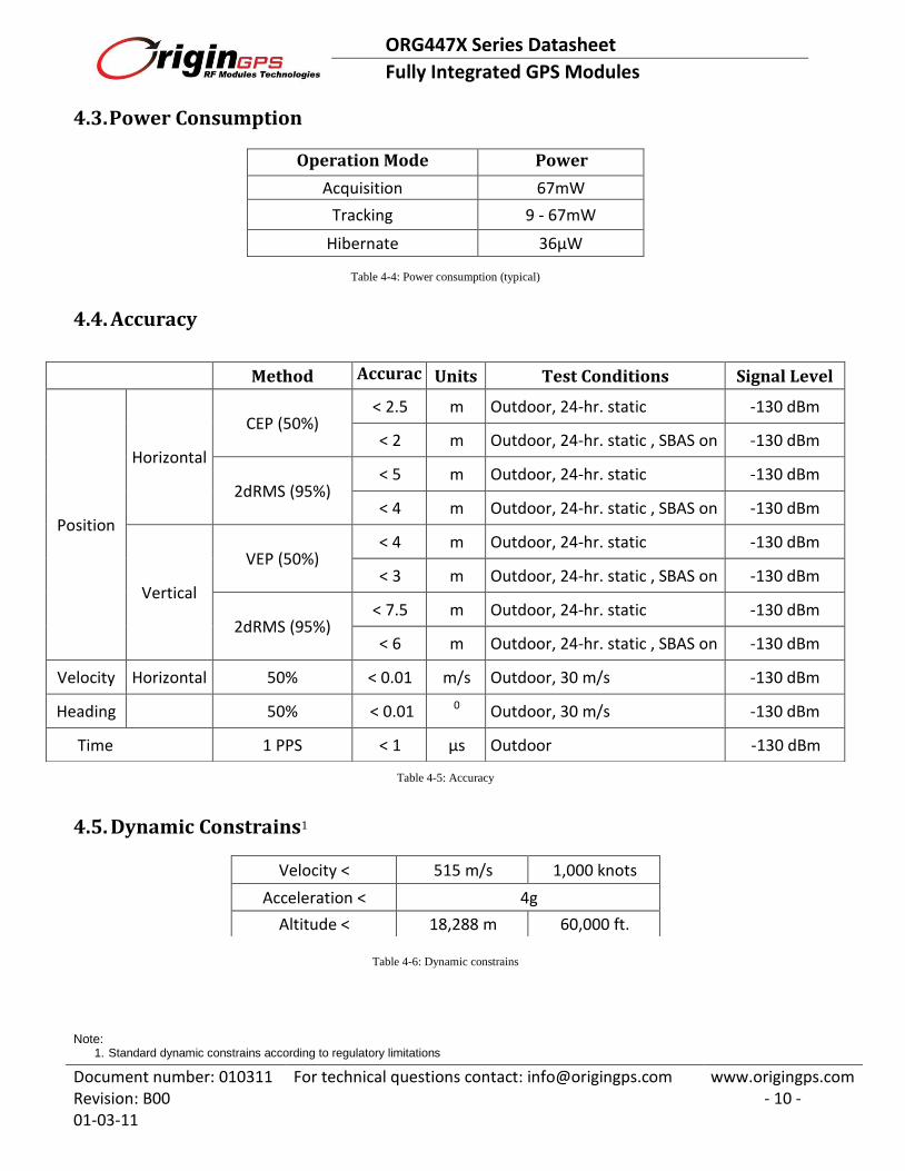
4.3. Power Consumption
Table 4-4: Power consumption (typical)
4.4. Accuracy
Table 4-5: Accuracy
4.5. Dynamic Constrains1
Table 4-6: Dynamic constrains
Note: 1. Standard dynamic constrains according to regulatory limitations
Operation Mode Power Consumption Acquisition 67mW
Tracking 9 - 67mW
Hibernate 36µW
Method Accuracy
Units Test Conditions Signal Level
Position
Horizontal
CEP (50%) < 2.5 m Outdoor, 24-hr. static -130 dBm
< 2 m Outdoor, 24-hr. static , SBAS on -130 dBm
2dRMS (95%) < 5 m Outdoor, 24-hr. static -130 dBm
< 4 m Outdoor, 24-hr. static , SBAS on -130 dBm
Vertical
VEP (50%) < 4 m Outdoor, 24-hr. static -130 dBm
< 3 m Outdoor, 24-hr. static , SBAS on -130 dBm
2dRMS (95%) < 7.5 m Outdoor, 24-hr. static -130 dBm
< 6 m Outdoor, 24-hr. static , SBAS on -130 dBm
Velocity Horizontal 50% < 0.01 m/s Outdoor, 30 m/s -130 dBm
Heading 50% < 0.01 0 Outdoor, 30 m/s -130 dBm
Time 1 PPS < 1 µs Outdoor -130 dBm
Velocity < 515 m/s 1,000 knots
Acceleration < 4g
Altitude < 18,288 m 60,000 ft.
ORG447X Series Datasheet
Fully Integrated GPS Modules
Document number: 010311 For technical questions contact: [email protected] www.origingps.com Revision: B00 01-03-11
- 11 -
5. Power Management
5.1. Power states
Full Power state (Acquisition/Tracking)
The module stays in full power until a position solution is made and estimated to be reliable. During the acquisition, processing is more intense than during tracking, thus consuming more power.
CPU Only state
This is the state when the RF and DSP sections are partially powered off. The state is entered when the satellites measurements have been acquired but the navigation solution still needs to be computed.
Standby state
This is the state when the RF and DSP sections are completely powered off and baseband clock is stopped.
Hibernate state
In this state the RF, DSP and baseband sections are completely powered off leaving only the RTC and Battery-Backed RAM running. The module will perform Hot Start if held in Hibernate state less than 2 hours after valid position solution was acquired.
5.2. Power saving modes
The ORG447X series has three power management modes available in modules with Basic and Standard firmware – ATP™, APM™ and PTF™ and additional SiRFAware™ Micro Power Mode (MPM™) available in modules with Premium firmware which are controlled by internal state machine. These modes provide different levels of power saving with different degradation level of position accuracy.
ORG447X Series Datasheet
Fully Integrated GPS Modules
Document number: 010311 For technical questions contact: [email protected] www.origingps.com Revision: B00 01-03-11
- 12 -
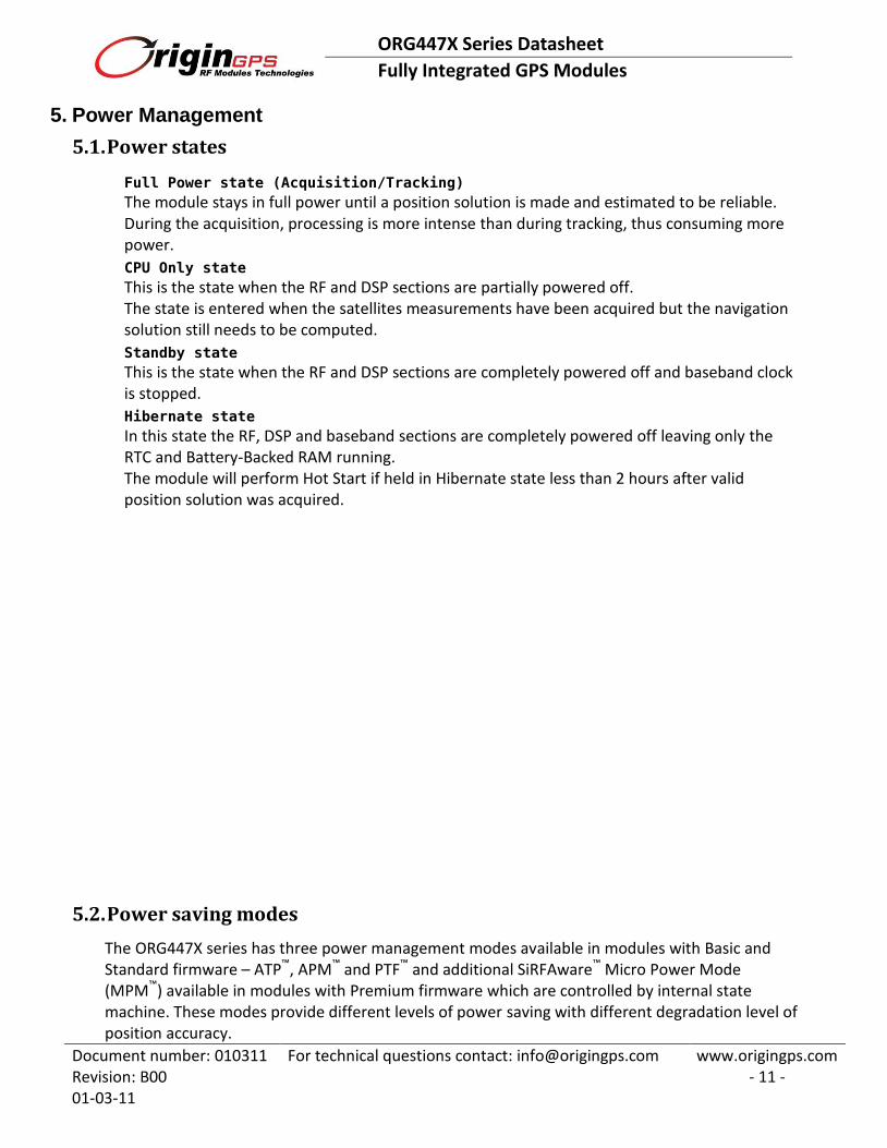
Adaptive Trickle Power (ATP™)
Adaptive Trickle Power (ATP™) is best suited for applications that require navigation solutions at a fixed rate as well as low power consumption and an ability to track weak signals. This power saving mode provides the most accurate positioning. In ATP™ mode the ORG447X series module is intelligently cycled between Full Power, CPU Only and Standby states to optimize low power operation.
Figure 5-1: ATP™ timing
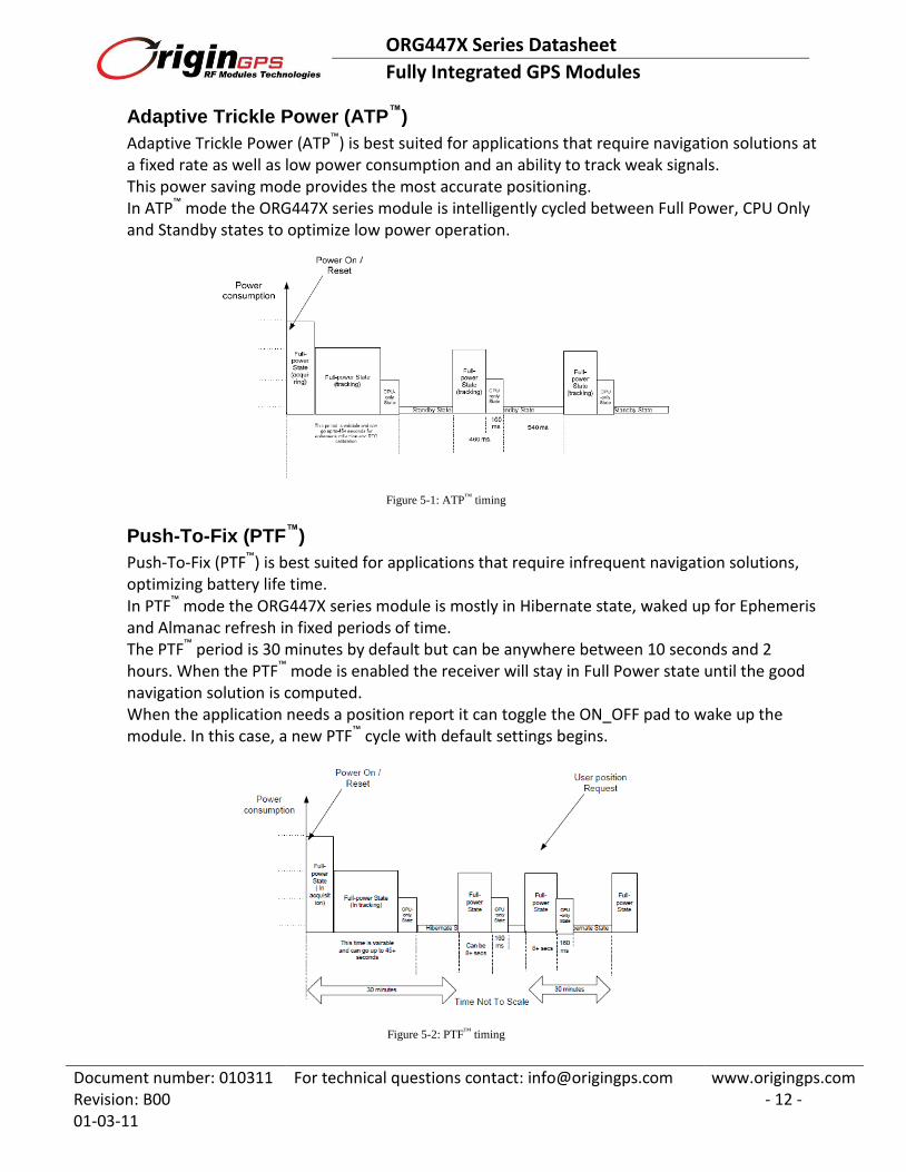
Push-To-Fix (PTF™)
Push-To-Fix (PTF™) is best suited for applications that require infrequent navigation solutions, optimizing battery life time. In PTF™ mode the ORG447X series module is mostly in Hibernate state, waked up for Ephemeris and Almanac refresh in fixed periods of time. The PTF™ period is 30 minutes by default but can be anywhere between 10 seconds and 2 hours. When the PTF™ mode is enabled the receiver will stay in Full Power state until the good navigation solution is computed. When the application needs a position report it can toggle the ON_OFF pad to wake up the module. In this case, a new PTF™ cycle with default settings begins.
Figure 5-2: PTF™ timing
ORG447X Series Datasheet
Fully Integrated GPS Modules
Document number: 010311 For technical questions contact: [email protected] www.origingps.com Revision: B00 01-03-11
- 13 -
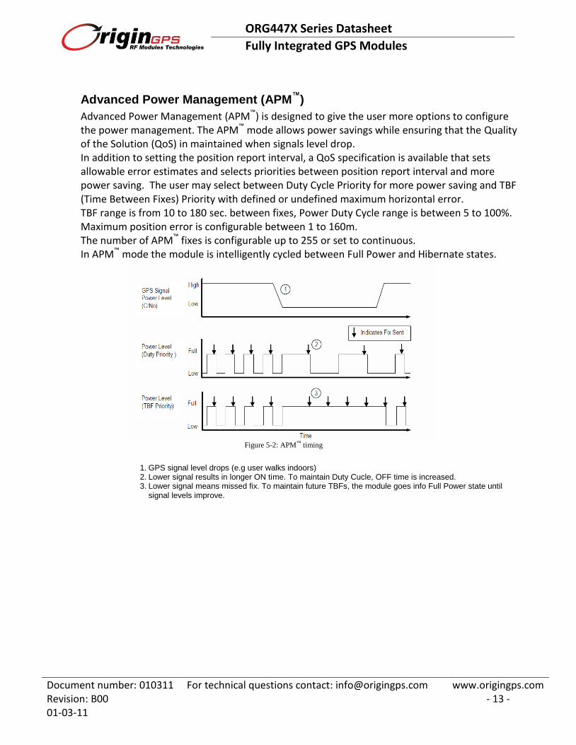
Advanced Power Management (APM™)
Advanced Power Management (APM™) is designed to give the user more options to configure the power management. The APM™ mode allows power savings while ensuring that the Quality of the Solution (QoS) in maintained when signals level drop. In addition to setting the position report interval, a QoS specification is available that sets allowable error estimates and selects priorities between position report interval and more power saving. The user may select between Duty Cycle Priority for more power saving and TBF (Time Between Fixes) Priority with defined or undefined maximum horizontal error. TBF range is from 10 to 180 sec. between fixes, Power Duty Cycle range is between 5 to 100%. Maximum position error is configurable between 1 to 160m. The number of APM™ fixes is configurable up to 255 or set to continuous. In APM™ mode the module is intelligently cycled between Full Power and Hibernate states.
Figure 5-2: APM™ timing
1. GPS signal level drops (e.g user walks indoors) 2. Lower signal results in longer ON time. To maintain Duty Cucle, OFF time is increased. 3. Lower signal means missed fix. To maintain future TBFs, the module goes info Full Power state until
signal levels improve.
ORG447X Series Datasheet
Fully Integrated GPS Modules
Document number: 010311 For technical questions contact: [email protected] www.origingps.com Revision: B00 01-03-11
- 14 -
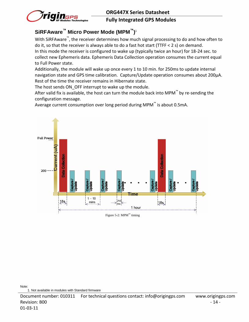
SiRFAware™ Micro Power Mode (MPM™)1
With SiRFAware™, the receiver determines how much signal processing to do and how often to do it, so that the receiver is always able to do a fast hot start (TTFF < 2 s) on demand. In this mode the receiver is configured to wake up (typically twice an hour) for 18-24 sec. to collect new Ephemeris data. Ephemeris Data Collection operation consumes the current equal to Full Power state. Additionally, the module will wake up once every 1 to 10 min. for 250ms to update internal navigation state and GPS time calibration. Capture/Update operation consumes about 200µA. Rest of the time the receiver remains in Hibernate state. The host sends ON_OFF interrupt to wake up the module. After valid fix is available, the host can turn the module back into MPM™ by re-sending the configuration message. Average current consumption over long period during MPM™ is about 0.5mA.
Figure 5-2: MPM™ timing
Note:
1. Not available in modules with Standard firmware
ORG447X Series Datasheet
Fully Integrated GPS Modules
Document number: 010311 For technical questions contact: [email protected] www.origingps.com Revision: B00 01-03-11
- 15 -
6. Extended Features
6.1. Almanac Based Positioning (ABP™)1 With ABP™ mode enabled, the user can get shorter Cold Start TTFF as a tradeoff with the position error. When no sufficient Ephemeris data is available to calculate an accurate solution, a coarse solution will be provided where the position is calculated based on one or more of the SVs having their states derived from Almanac data. Almanac data for ABP™ purposes may be stored factory set, broadcasted or pushed.
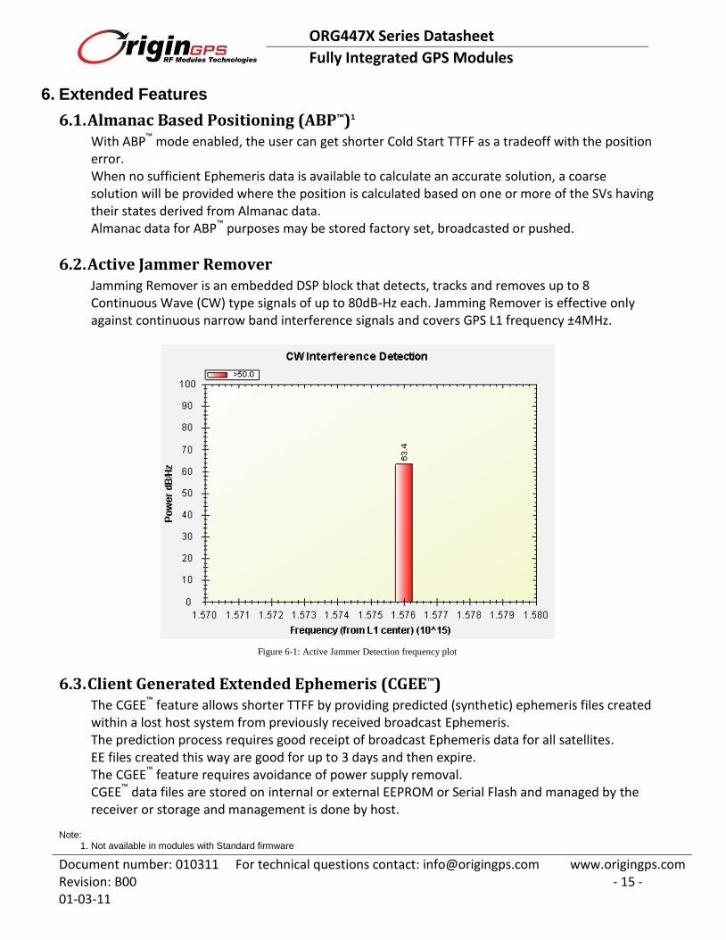
6.2. Active Jammer Remover Jamming Remover is an embedded DSP block that detects, tracks and removes up to 8 Continuous Wave (CW) type signals of up to 80dB-Hz each. Jamming Remover is effective only against continuous narrow band interference signals and covers GPS L1 frequency ±4MHz.
Figure 6-1: Active Jammer Detection frequency plot
6.3. Client Generated Extended Ephemeris (CGEE™) The CGEE™ feature allows shorter TTFF by providing predicted (synthetic) ephemeris files created within a lost host system from previously received broadcast Ephemeris. The prediction process requires good receipt of broadcast Ephemeris data for all satellites. EE files created this way are good for up to 3 days and then expire. The CGEE™ feature requires avoidance of power supply removal. CGEE™ data files are stored on internal or external EEPROM or Serial Flash and managed by the receiver or storage and management is done by host.
Note:
1. Not available in modules with Standard firmware
ORG447X Series Datasheet
Fully Integrated GPS Modules
Document number: 010311 For technical questions contact: [email protected] www.origingps.com Revision: B00 01-03-11
- 16 -
7. Interface
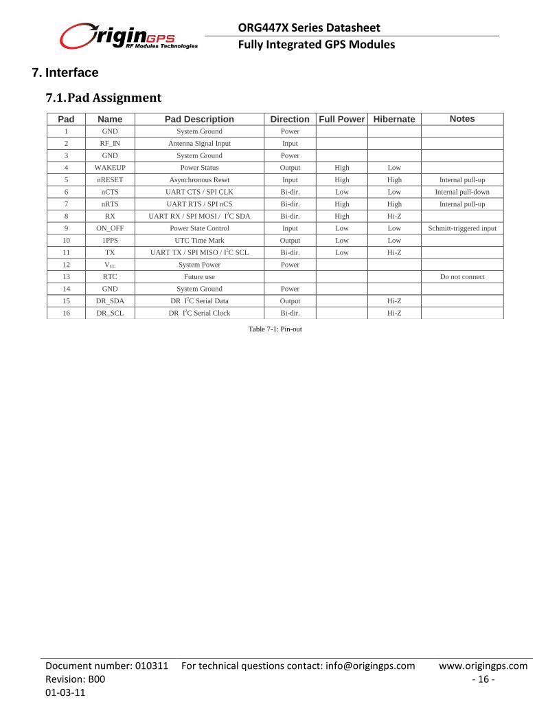
7.1. Pad Assignment
Table 7-1: Pin-out
Notes Hibernate Full Power Direction Pad Description Name Pad
Power System Ground GND 1
Input Antenna Signal Input RF_IN 2
Power System Ground GND 3
Low High Output Power Status WAKEUP 4
Internal pull-up High High Input Asynchronous Reset nRESET 5
Internal pull-down Low Low Bi-dir. UART CTS / SPI CLK nCTS 6
Internal pull-up High High Bi-dir. UART RTS / SPI nCS nRTS 7
Hi-Z High Bi-dir. UART RX / SPI MOSI / I2C SDA RX 8
Schmitt-triggered input Low Low Input Power State Control ON_OFF 9
Low Low Output UTC Time Mark 1PPS 10
Hi-Z Low Bi-dir. UART TX / SPI MISO / I2C SCL TX 11
Power System Power VCC 12
Do not connect Future use RTC 13
Power System Ground GND 14
Hi-Z Output DR I2C Serial Data DR_SDA 15
Hi-Z Bi-dir. DR I2C Serial Clock DR_SCL 16

ORG447X Series Datasheet
Fully Integrated GPS Modules
Document number: 010311 For technical questions contact: [email protected] www.origingps.com Revision: B00 01-03-11
- 17 -
7.2. Connectivity
7.2.1. Power
Power supply
The ORG447X series module requires only one power supply VCC of 1.8V DC. It is recommended to keep the power supply on all the time in order to maintain the non-volatile RTC and RAM active for fastest possible TTFF. When powering the ORG447X module from switching mode (DC-DC) power supply carefully follow manufacturer’s application notes and apply filtering to minimize ripple. Voltage ripple below 300mVPP allowed for frequency under 10KHz. Voltage ripple below 100mVPP allowed for frequency between 10KHz and 100KHz. Voltage ripple below 50mVPP allowed for frequency between 100KHz and 1MHz. Voltage ripple below 10mVPP allowed for frequency above 1MHz. Higher voltage ripple may compromise the ORG447X module performance. When the VCC is powered off settings are reset to factory default and the receiver performs Cold Start on next power up. Power supply current varies according to the processor load and satellite acquisition. Typical ICC current is 40mA during acquisition. Peak ICC current is 55mA. Typical ICC current in Hibernate state is 20µA.
Ground
All Ground pads should be connected to the main Ground plane with shortest possible traces or vias.

ORG447X Series Datasheet
Fully Integrated GPS Modules
Document number: 010311 For technical questions contact: [email protected] www.origingps.com Revision: B00 01-03-11
- 18 -
7.2.2. Host Control Interface
ON OFF control input
The ON_OFF control input can be used to switch the receiver between Normal or Hibernate states and also to generate interrupt in PTF™ mode. The ON_OFF interrupt is generated by a low-high-low toggle, which should be longer than 62µs and less than 1s (100ms pulse length recommended). ON_OFF interrupts with less than 1 sec intervals are not recommended. Multiple switch bounce pulses are recommended to be filtered out. ON_OFF input is 3.6V tolerant. Pull-down resistor of 33kΩ-82kΩ is recommended. Must be connected to host.
Figure 7-1: ON_OFF timing
nRESET input
The Power-on-Reset (POR) is generated internally in the ORG447X module. Additionally, manual reset option is available through nRESET pad. Resetting the module clears the RTC block and configuration settings become default. nRESET pad is active low and has internal pull-up resistor of 86kΩ (typ.). nRESET signal should be applied for at least 1µs. Do not drive nRESET input high. Do not connect if not in use.
WAKEUP output
The WAKEUP pad is an output from the ORG447X used to flag for power mode. A low on this output indicates that the module is in one of its low-power states - Hibernate or Standby. A high on this output indicates that the module is in Full Power operating mode. WAKEUP output can be used to control enable of auxiliary devices, like level translator, active antenna bias, or to flag for high current demand from power supply. Wakeup output is LVCMOS 1.8V compatible.
1PPS output
The pulse-per-second (PPS) output provides a pulse signal for timing purposes. Pulse length (high state) is 200ms, and less than 1µs synchronized to full UTC second. The UTC time message is generated and put into output FIFO 300ms after PPS rising edge. The exact time between the PPS and UTC time message delivery depends on message rate, message queue and communication baud rate. 1PPS output is LVCMOS 1.8V compatible. Do not connect if not in use.

ORG447X Series Datasheet
Fully Integrated GPS Modules
Document number: 010311 For technical questions contact: [email protected] www.origingps.com Revision: B00 01-03-11
- 19 -
7.2.3. Host Data Interface
The ORG447X has 3 types of interface ports to connect to host: UART, SPI and I2C. All ports are multiplexed on a shared set of pads. At system reset, the host port interface lines are disabled, so no conflict occurs. Configuration straps on nCTS and nRTS are read by the module firmware during startup and define port type. Use 10kΩ resistor for external strap.
Port Type nCTS nRTS
UART External pull-up Internal pull-up
SPI (default) Internal pull-down Internal pull-up
I2C Internal pull-down External pull-down
Table 7-2: ORG447X host interface selection
UART
The module has a 4-wire UART port:
TX used for GPS data reports.
RX used for receiver control.
nCTS and nRTS are optionally used for hardware flow control. The default protocol is NMEA@4,800bps 8-N-1 (8 data bits, No parity, 1 stop bit). The configuration for baud rates and respective protocols can be changed by commands via NMEA or OSP (SiRF Binary) protocols. Baud rates are configurable from 900bps to 1.8Mbps.
Table 7-3: ORG447X UART baud rate tolerance
Outputs are LVCMOS 1.8V compatible. Inputs are 3.6V tolerant.
Figure 7-2: UART integrity
Baud Rate (bps) Error (%) Baud Rate (bps) Error (%) Baud Rate (bps) Error (%)
900 0.00 14400 0.62 230400 1.04
1200 0.00 19200 0.00 307200 0.01
1800 0.00 28800 0.00 460800 0.60
2400 0.00 38400 0.07 614400 1.10
3600 0.00 57600 0.64 921600 2.30
4800 0.06 76800 0.01 1228800 0.07
7200 0.00 115200 0.24 1843200 0.86
9600 0.00 153600 0.03
ORG447X Series Datasheet
Fully Integrated GPS Modules
Document number: 010311 For technical questions contact: [email protected] www.origingps.com Revision: B00 01-03-11
- 20 -
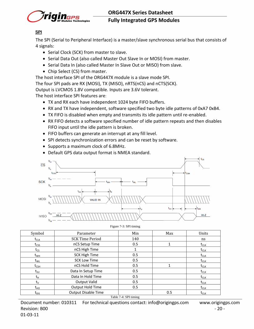
SPI
The SPI (Serial to Peripheral Interface) is a master/slave synchronous serial bus that consists of 4 signals:
Serial Clock (SCK) from master to slave.
Serial Data Out (also called Master Out Slave In or MOSI) from master.
Serial Data In (also called Master In Slave Out or MISO) from slave.
Chip Select (CS) from master. The host interface SPI of the ORG447X module is a slave mode SPI. The four SPI pads are RX (MOSI), TX (MISO), nRTS(nCS) and nCTS(SCK). Output is LVCMOS 1.8V compatible. Inputs are 3.6V tolerant. The host interface SPI features are:
TX and RX each have independent 1024 byte FIFO buffers.
RX and TX have independent, software specified two byte idle patterns of 0xA7 0xB4.
TX FIFO is disabled when empty and transmits its idle pattern until re-enabled.
RX FIFO detects a software specified number of idle pattern repeats and then disables FIFO input until the idle pattern is broken.
FIFO buffers can generate an interrupt at any fill level.
SPI detects synchronization errors and can be reset by software.
Supports a maximum clock of 6.8MHz.
Default GPS data output format is NMEA standard.
Figure 7-3: SPI timing
Symbol Parameter Min Max Units
tCLK SCK Time Period 140
ns
tCSS nCS Setup Time 0.5 1 tCLK
tCS nCS High Time 1
tCLK
tWH SCK High Time 0.5
tCLK
tWL SCK Low Time 0.5
tCLK
tCSH nCS Hold Time 0.5 1 tCLK
tSU Data In Setup Time 0.5
tCLK
tH Data In Hold Time 0.5
tCLK
tV Output Valid 0.5
tCLK
tHO Output Hold Time 0.5
tCLK
tDIS Output Disable Time
0.5 tCLK Table 7-4: SPI timing

ORG447X Series Datasheet
Fully Integrated GPS Modules
Document number: 010311 For technical questions contact: [email protected] www.origingps.com Revision: B00 01-03-11
- 21 -
Operation:
The SPI performs bit-by-bit transmitting and receiving at the same time whenever nCS is asserted and SCK is active. In order to communicate properly with SPI device, the protocol must be agreed – specifically- SPI mode and an idle byte pattern. Among 4 SPI modes of the clock polarity (CPOL) and clock phase (CPHA) only SPI Mode 1 <CPOL=”0”, CPHA =”1”> has been tested:
At CPOL=”0” the base value of the clock is zero.
For CPHA=”1”, data are read on the clock's falling edge and data are changed on a rising edge. On power up, the first message to come out of the module is the “OK_TO_SEND” message. It takes about 20ms from power up for the module SPI drivers to get initialized. The slave has no way of forcing data to the master to indicate it is ready for transmission - the master must poll the client periodically. Since the specified idle 2-byte pattern for both receive and transmit is 0xA7 0xB4, the master can transmit this idle pattern into the slave repeatedly. If the master receives idle patterns back from the slave, it indicates that the slave currently has nothing to transmit but is ready to communicate. On the module receive side, the host is expected to transmit idle pattern when it is querying the module’s transmit buffer. In this way, the volume of discarded bytes is kept nearly as low as in the UART implementation because the module hardware does not place most idle pattern bytes in its RX FIFO. Most messaging can be serviced with polling. The FIFO thresholds are placed to detect large messages requiring interrupt-driven servicing. On the module transmit side the intent is to fill the FIFO only when it is disabled and empty. In this condition, the module’s SPI driver software loads as many queued messages as can completely fit in the FIFO. Then the FIFO is enabled. The host is required to poll messages until idle pattern bytes are detected. At this point the module’s FIFO is empty and disabled, allowing the ORG447X SPI driver to again respond to an empty FIFO interrupt and load the FIFO with any messages in queue. Notes: For SPI communication, read and write operations both require data being sent to the Slave SPI (idle bytes for reads and message data for writes). Any time data is sent to the module via the SPI bus, the Slave SPI of the module will send an equal amount of data back to the host. These bytes must be buffered either in hardware or software, and it is up to the host to determine if the bytes received may be safely discarded (idle bytes), or should be passed on to the application handling GPS communication. Failure to properly handle data received from the SPI slave can result in corrupted GPS messages. The external SPI master may send idle bytes and complete messages in a single transmission, provided that idle bytes shall not be inserted inside of a message. The idle byte pattern and repeat count prevents the problem of messages lost due to normal occurrence of idle byte patterns within message data with high probability. The external SPI master shall not send partial messages. All transmissions from the SPI master shall be in multiples of 8 bits. The external SPI master shall transmit the idle byte pattern when reading the SPI slave's transmit buffer when the master has no message data to transmit. The SPI slave shall be serviced at a rate that will keep the TX FIFO empty.
ORG447X Series Datasheet
Fully Integrated GPS Modules
Document number: 010311 For technical questions contact: [email protected] www.origingps.com Revision: B00 01-03-11
- 22 -
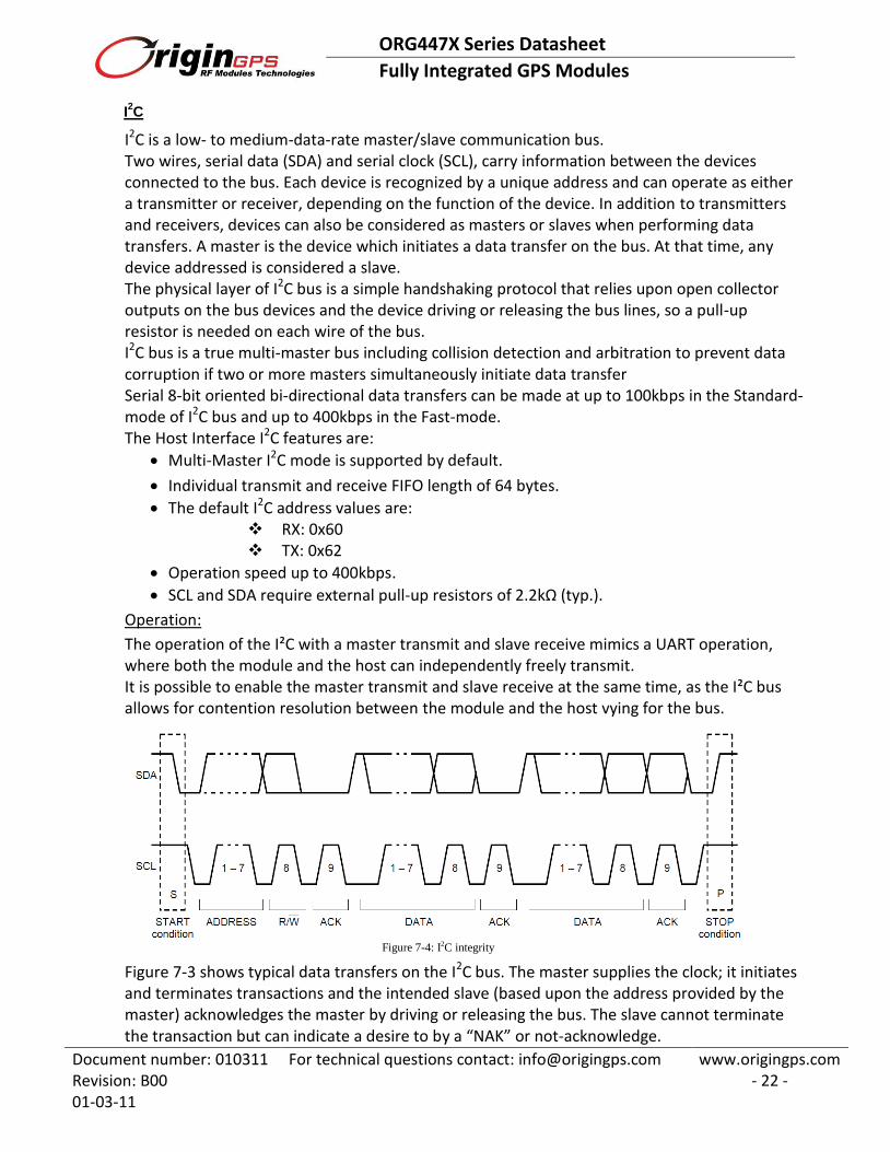
I2C
I2C is a low- to medium-data-rate master/slave communication bus. Two wires, serial data (SDA) and serial clock (SCL), carry information between the devices connected to the bus. Each device is recognized by a unique address and can operate as either a transmitter or receiver, depending on the function of the device. In addition to transmitters and receivers, devices can also be considered as masters or slaves when performing data transfers. A master is the device which initiates a data transfer on the bus. At that time, any device addressed is considered a slave. The physical layer of I2C bus is a simple handshaking protocol that relies upon open collector outputs on the bus devices and the device driving or releasing the bus lines, so a pull-up resistor is needed on each wire of the bus. I2C bus is a true multi-master bus including collision detection and arbitration to prevent data corruption if two or more masters simultaneously initiate data transfer Serial 8-bit oriented bi-directional data transfers can be made at up to 100kbps in the Standard-mode of I2C bus and up to 400kbps in the Fast-mode. The Host Interface I2C features are:
Multi-Master I2C mode is supported by default.
Individual transmit and receive FIFO length of 64 bytes.
The default I2C address values are: RX: 0x60 TX: 0x62
Operation speed up to 400kbps.
SCL and SDA require external pull-up resistors of 2.2kΩ (typ.).
Operation:
The operation of the I²C with a master transmit and slave receive mimics a UART operation, where both the module and the host can independently freely transmit. It is possible to enable the master transmit and slave receive at the same time, as the I²C bus allows for contention resolution between the module and the host vying for the bus.
Figure 7-4: I2C integrity
Figure 7-3 shows typical data transfers on the I2C bus. The master supplies the clock; it initiates and terminates transactions and the intended slave (based upon the address provided by the master) acknowledges the master by driving or releasing the bus. The slave cannot terminate the transaction but can indicate a desire to by a “NAK” or not-acknowledge.

ORG447X Series Datasheet
Fully Integrated GPS Modules
Document number: 010311 For technical questions contact: [email protected] www.origingps.com Revision: B00 01-03-11
- 23 -
I2C specification defines unique situations as START (S) and STOP (P) conditions. A HIGH to LOW transition on the SDA line while SCL is HIGH indicates a START condition. A LOW to HIGH transition on the SDA line while SCL is HIGH defines a STOP condition. START and STOP conditions are always generated by the master. Every byte put on the SDA line must be 8-bits long. The number of bytes can be transmitted per transfer is unrestricted. Each byte is followed by an acknowledge bit. Data is transferred with the Most Significant Bit (MSB) first. In most cases, data transfer with acknowledge is obligatory. The acknowledge–related clock pulse is generated by the master. The transmitter releases the SDA line (HIGH) during the acknowledge clock pulse. The receiver must pull down the SDA line during the acknowledge clock pulse so that it remains stable LOW during the HIGH period of this clock pulse. Set-up and hold times must be taken into account. All data transfers of I2C specification should follow the format. After the START condition (S), a slave address should be sent first. This address is 7 bits long followed by an 8-th bit which is a data direction bit (R/nW) – logical 0 indicates a transmission (WRITE), logical 1 indicates a request for data (READ). After the slave address byte is sent, master can continue its data transfer by writing or reading data byte as defined format. The data transfer is always terminated by a STOP condition generated by the master.
Figure 7-5: I2C timing
Symbol Parameter Min Max Units fSCL SCL frequency 100 400 kHz
tHD;STA Hold Time for START condition 0.6
µs
tLOW Low Time of SCL 1.3
µs
tHIGH High Time of SCL 0.6
µs
tSU;STA Setup Time for START condition 0.6
µs
tHD;DAT Hold Time 0 0.9 µs
tSU;DAT Data Setup Time 0.1
µs
tr Rise Time of SDA and SCL
0.3 µs
tf Fall Time of SDA and SCL
0.3 µs
tSU;STO Setup Time for STOP condition 0.6
µs
tBUF Bus Free Time between START and STOP 1.3
µs CL Capacitive Load of SDA and SCL
400 pF
VnL Noise Margin at the low logic level
0.1·VCC V VnH Noise Margin at the high logic level
0.2·VCC V
Table 7-5: I2C timing
ORG447X Series Datasheet
Fully Integrated GPS Modules
Document number: 010311 For technical questions contact: [email protected] www.origingps.com Revision: B00 01-03-11
- 24 -
7.2.4. Smart Sensors Data Interface
The ORG447X master mode I²C interface provides support for dead reckoning (DR) and code patch upload (optional). The port has 2 pads, DR_SCL and DR_SDA, both pins are pseudo open-drain and require pull-up resistors on the external bus.
Dead Reckoning (DR) I²C Interface
The DR I²C interface supports required sensor instruments for dead reckoning applications such as gyros, accelerometers, compasses or other sensors that can operate with an I²C bus. The ORG447X module acts as the I2C Master and the sensor devices function in Slave mode. This provides a very low latency data pipe for the critical sensor data so that it can be used in the Navigation Library and Kalman filter to enhance navigation performance. The MEMS algorithms perform a sensor data fusion with the GPS signal measurements. GPS measurements can be used to calibrate the MEMS sensors during periods of GPS navigation. The MEMS sensors can augment GPS measurements, and can be more accurate than GPS under degraded GPS signal conditions and certain dynamics. DR I²C interface supports:
Common sensor formats
Typical data lengths (command + in/data out) of several bytes
Standard I²C bus maximum data rate 400kbps
Minimum data rate 100kbps In current Premium firmware implementation, MEMS sensors integration provides a pseudo “position pinning” feature to prevent position wander and heading instability.
Data Storage Support
The DR I²C interface is available at boot-up for uploading data from a serial EEPROM. Firmware updates may be provided from time to time to address ROM firmware issues as a method of performance improvement. The DR I²C interface also supports serial flash devices used to store ARM7TDMI patch loads, including optional:
FIFO support
ARM7TDMI dedication to I²C interface during serial flash read or write
7.2.5. RF input
The antenna input impedance is 50Ω. The input is DC blocked. The module supports active and passive antennas. In design with passive antenna attention should be paid on antenna layout. Short trace with controlled impedance of 50Ω should conduct GPS signal from antenna to RF_IN pad. In designs with active antenna DC bias voltage should be applied on RF_IN through AC blocking inductor. DC bias voltage can be controlled by WAKEUP output through MOSFET or load switch. In designs with active antenna net gain including conductors losses should not exceed 25dB. In designs with external LNA, LNA enable input can be controlled by the ORG447X WAKEUP output.

ORG447X Series Datasheet
Fully Integrated GPS Modules
Document number: 010311 For technical questions contact: [email protected] www.origingps.com Revision: B00 01-03-11
- 25 -
7.3. Typical Application Circuit 7.3.1. Minimal Schematic Diagrams
UART Host Interface
Figure 7-6: UART interface circuit
SPI Host Interface
Figure 7-7: SPI interface circuit
I2C Host Interface
Figure 7-8: I2C interface circuit
TX_GPS
TX
RXRX_GPS
R4 220R
R5 220R
C3
18pF
C2
18pF
RX
TX
U1
ORG447X
GPS Module
ORIGINGPS
LGA77
TX11
RX8
CTS6
Vcc
12
GND1
GND3
GND
14
RESET5
ON_OFF9
1PPS10
RTS7RF_IN
2
WAKEUP4 DR_SCL
16
DR_SDA15
13RTC
NEP
17
50 Ohm microstrip
GPS_ON
GPS_ON
RF_IN
ON_OFF
C1
1uF
R3
47K
R2 220R
ANTENNA
GPS_ON
V_1V8
R1
10K
V_1V8
GPS_MISO
GPS_MOSI
R5 220R
R6 220R
SPI_CLK
U1
ORG447X
GPS Module
ORIGINGPS
LGA77
TX11
RX8
CTS6
Vcc
12
GND1
GND3
GND
14
RESET5
ON_OFF9
1PPS10
RTS7RF_IN
2
WAKEUP4 DR_SCL
16
DR_SDA15
13RTC
NEP
17
50 Ohm microstrip
ON_OFFGPS_ON
RF_IN
C1
1uF
R2
47K
R1 220R
ANTENNA
V_1V8
GPS_CLK
GPS_nCS
R3 220R
R4 220RSPI_nCS
GPS_ONGPS_ON
SPI_MOSI
SPI_MISO
U1
ORG447X
GPS Module
ORIGINGPS
LGA77
TX11
RX8
CTS6
Vcc
12
GND1
GND3
GND
14
RESET5
ON_OFF9
1PPS10
RTS7RF_IN
2
WAKEUP4 DR_SCL
16
DR_SDA15
13RTC
NEP
17
50 Ohm microstrip
R2
2K2
R3
2K2I2C_SCL
V_1V8
I2C_SDA
GPS_ON
RF_IN
ON_OFFGPS_ON
C1
1uF
R5
47K
R4 220R
ANTENNA
GPS_ON
V_1V8
R1
10K
I2C_SCL
I2C_SDA

ORG447X Series Datasheet
Fully Integrated GPS Modules
Document number: 010311 For technical questions contact: [email protected] www.origingps.com Revision: B00 01-03-11
- 26 -
7.3.2. Extended Schematic Diagrams
1.8V LDO Regulator And Level Shifter
Figure 7-9: UART interface circuit
1.8V DC-DC Buck Regulator, Active Antenna Power Switch And Level Shifter
Figure 7-10: Active Antenna and UART interface circuit
RX
TX
nRESETnRESET
TX
(option)
nRESET
R1
10K
1PPS
GPS_ON
WAKEUP
EN_GPS
GPS_VCC
R5 220R
R4 220R U2
NLU1GT126CMX1ONSEMI
ULLGA6_1.0x1.0
2 4
5 316
C4
1uF
TX_GPS
WAKEUP
C2
18pF
1PPS
RX
C3
18pF
RX_GPS
VCC
EN_GPS
Vcc range 2V - 5.5V
C6
1uF
U31.8V LDO
TLV70018DDCTSOT23-5
TI
VIN1
GND
2
EN3
NC4
VOUT5
R6
47K
C5
1uF
GPS_VCC
VCCVCC
50 Ohm microstrip
RF_IN
ANTENNA
1PPS
EN_GPS
WAKEUP
ON_OFFGPS_ON
R3
47K
R2 220R
WAKEUP
GPS_ON
(option)
C1
1uF
GPS_VCC
U1
ORG447X
GPS Engine
ORIGINGPS
LGA77
TX11
RX8
CTS6
Vcc
12
GND1
GND3
GND
14
RESET5
ON_OFF9
1PPS10
RTS7RF_IN
2
WAKEUP4 DR_SCL
16
DR_SDA15
13RTC
NEP
17(option)
(option)
C8
18pF
nRTS
nCTS
RX
TX
Level Translator to Vio
Active Antenna Bias
nCTS
nRTSnRTS
nCTS
WAKEUP_GPS
TVS1
DNAINFINEONESD0P2RF-02LRH
L1
27nH
MURATALQG15HS27NJ02
R7 33R
C5
1uF
C7
4.7uF
U2
SON6_1.0x1.5
TITPS62231DRY
Vin3
EN5
GND
4
SW2
FB6
MODE1
L22.2uH
MURATALQM2HPN2R2MG0
Vcc range 2V - 6V
GPS_VCC
VCC
R4
47K
VCC
EN_GPS
C6
2.2uF
nRTS_GPS
SW
C4
1uFU3
TXB0104RUTRTI
UQFN-16
VCCA1
A12
A23
A34
A45
GND
6
OE
12
B47
B38
B29
B110
VCCB11
RX_GPS~
R5
47K
R9 220R
GPS_VCC
U1
__________________
Inputs are 1.8V - 3.6V
Outputs are 1.8V
NEP - Non Exposed Pad
ON_GPS
WAKEUP_GPS
1PPS_GPS
VCC
EN_GPS
ON_GPS
RX_GPS
RX
TX
GND
VCC
EN_GPS
1PPS_GPS
TX
RX
2V- 6V
ON_GPS
WAKEUP_GPS
(option)
(option)
(option)
nRESET_GPSnRESET_GPS
Vio
Vio
Vant
1.8V- 4V
Vant
1.62V- 5.5V
Vcc, Vant, Vio can be connected together if 2V<Vcc<4V
TX_GPS
J1RF Connector
ON_OFF
1PPS_GPS
nRESET_GPS
WAKEUP_GPS
C10
18pF
U4
ON
NTZD3155CT1GSOT-563
6Dn
2 GnSn 1
3Dp
5 GpSp 4
R8 33R
C3
18pFR3 33R
C11
18pF
BIAS_EN
TX_GPS~
RF_INnCTS_GPS nCTS_GPS~
Vant
R2 33R
R1
10K
DNA = Do Not Assemble
Vant
R6
100K
GPS_VCCGPS_VCC
C2
18pF
C9
1uF
Vio
WAKEUP_GPS
nRTS_GPS~
U1
ORG447X
GPS Engine
ORIGINGPS
LGA77
TX11
RX8
CTS6
Vcc
12
GND1
GND3
GND
14
RESET5
ON_OFF9
1PPS10
RTS7RF_IN
2
WAKEUP4 DR_SCL
16
DR_SDA15
13RTC
NEP
17
ESD Protection Option
ORG447X Series Datasheet
Fully Integrated GPS Modules
Document number: 010311 For technical questions contact: [email protected] www.origingps.com Revision: B00 01-03-11
- 27 -
8. PCB Layout
8.1. Footprint
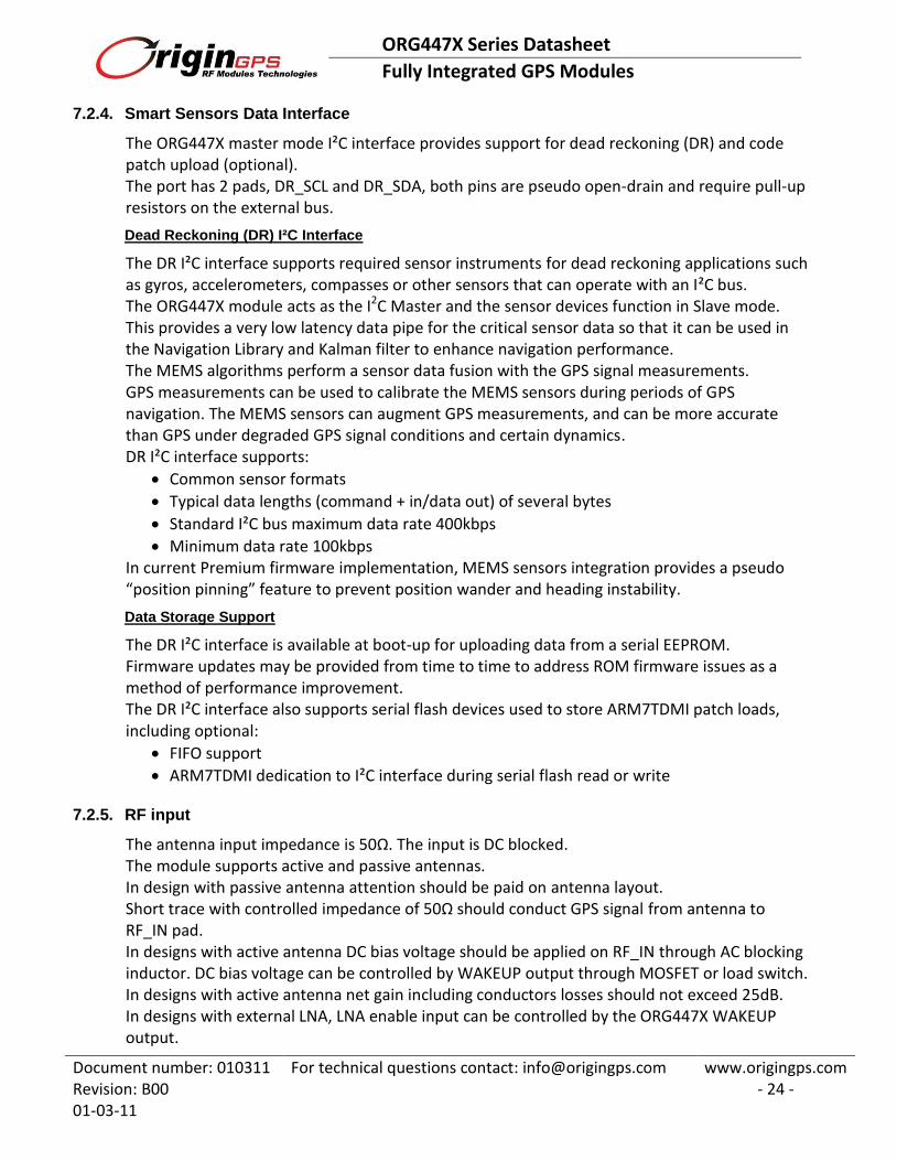
Figure 8-1: Footprint
Ground pad at the middle should be connected to main Ground plane by multiple vias. Ground pad at the middle should be solder masked. Silk print of module’s outline is highly recommended for SMT visual inspection.
8.2. RF Input trace
0.002
0.051 0.008
0.2040.005
0.127inch
millimeter Figure 8-2: Typical Microstrip PCB trace on FR-4 substrate
8.3. PCB stack up
Signals
Signals or Power
Ground
CS
PS
LN
.
.
.
Ground
GroundL2
Signals
controlled
impedance 50Ω
Figure 8-3: Typical PCB stack up
8.4. Design restrictions Keep out of signal or switching power traces and vias under the ORG447X module. Signal traces to/from ORG447X module should have minimum length. Recommended distance from adjacent active components is 3mm. In case of adjacent high speed components, like CPU or memory, high frequency components, like transmitters, clock resonators or oscillators, metal planes, like LCD or battery enclosures, please contact OriginGPS for more precise, application specific recommendations.
1
0.276
7.01
0.27
6
7.01
0.05
1.27
0.226
5.74
0.186
4.72
0.18
6
4.72
0.040
1.016
0.045
1.143 0.025
0.635
0.306
7.77

ORG447X Series Datasheet
Fully Integrated GPS Modules
Document number: 010311 For technical questions contact: [email protected] www.origingps.com Revision: B00 01-03-11
- 28 -
9. Operation
When power is first applied, the ORG447X goes into a Hibernate state while integrated RTC starts and
internal FSM sequences though to “Ready-to-Start” state.
The host is not required to control external master nRESET since module’s internal reset circuitry
handles detection of application of power.
While in “Ready-to-Start” state, the module awaits a pulse to the ON_OFF input.
Since integrated RTC startup times are variable, detection of when the ORG447X is ready to accept an
ON_OFF pulse requires the host to either wait for a fixed interval, to monitor a pulse on module
WAKEUP output that indicates FSM “Ready-to-Start”
Another option is to assert a pulse on the ON_OFF input every second until the ORG447X module
starts by indicating a high on WAKEUP or generation of UART messages.
9.1. Starting the ORG447X series module
A pulse on the ON_OFF input line when ORG447X FSM is ready and in startup-ready state,
Hibernate state, standby state, will command the module to start.
ON_OFF pulse requires a rising edge and high level that persists for at least 100 µs in order to be
detected. Resetting the ON_OFF detector requires that ON_OFF go to logic low at least 100 µs.
If the system is in Hibernate state, an ON_OFF pulse will move to Full Power mode
If the system is in Trickle Power Mode, an ON_OFF pulse will move it to Full Power mode.
If the system is in Push-To-Fix mode, an ON_OFF pulse will initiate one Push-To-Fix cycle.
If the system is already in Full Power mode, an ON_OFF pulse will initiate orderly shutdown.
Figure 9-1: Startup timing

ORG447X Series Datasheet
Fully Integrated GPS Modules
Document number: 010311 For technical questions contact: [email protected] www.origingps.com Revision: B00 01-03-11
- 29 -
Symbol Parameter Condition Min Typ Max Units fRTC RTC frequency 25
0C -20 ppm 32768 +20 ppm Hz
tRTC RTC tick 250C
30.5176
µs
∆T1 RTC startup time
300
ms
∆T0 Power stabilization 6·tRTC+∆T1 7·tRTC+∆T1 8·tRTC+∆T1 µs
∆T6 WAKEUP pulse RTC running
10
tRTC
∆TLOW ON_OFF low 3
tRTC
∆THIGH ON_OFF high 3
tRTC
∆T3 Startup sequencing After ON_OFF
1024
tRTC
- ON_OFF to WAKEUP high After ON_OFF
6
tRTC
∆T5 ON_OFF to ARM start After ON_OFF
2130
tRTC
∆T7 Main power source start1
WAKEUP high 0 30 300 tRTC
Table 9-1: Startup timing
Note:
1. When power provided through dual supply. Low quescent current 1.8V source (LDO) for Hibernate state, and high efficiency 1.8V source (DC-DC) for Full Power state. The main power supply should be able to provide current for Full Power state within 1ms after WAKEUP is high.
9.2. Verifying the ORG447X series module has started
The ORG447X module WAKEUP output will go high indicating the internal processor has started. System activity indication depends upon the serial interface chosen. UART: With no flow control - when active, the module will output NMEA messages at the 4800bps. With flow control - nCTS must be released by host to allow the module to send messages.
I2C: In Multi-Master mode with no bus contention - the module will spontaneously send messages
at the speed and message types selected. In Multi-Master mode with bus contention - the module will send messages after the I2C bus
contention resolution process allows it to send. SPI: Since the module is SPI slave, there is no possible indication of system “ready” through SPI
interface. The host must initiate SPI connection approximately one second after WAKEUP goes high.
9.3. Shutting down the ORG447X series module
Transferring the ORG447X module into Hibernate mode can be initiated in two ways:
By a pulse on the ON_OFF input when the ORG447X module in Full Power mode
By serial messages in OSP (MID205) or NMEA ($PSRF117) The orderly shutdown may take anywhere from 10ms to 900ms to complete, depending upon operation in progress and messages pending, and hence is dependent upon serial interface speed and controls.

ORG447X Series Datasheet
Fully Integrated GPS Modules
Document number: 010311 For technical questions contact: [email protected] www.origingps.com Revision: B00 01-03-11
- 30 -
10. Software Functions
The module supports NMEA-0183 ASCII protocol and One Socket Protocol (based on SiRF Binary Standard).
Power On State Hibernate
Default Interface1 SPI
SPI data format NMEA
UART data format NMEA
UART settings 4,800 bps 8-N-1
I2C data format NMEA
NMEA Messages
$GPGGA @1 sec.
$GPGSA @ 1 sec.
$GPGSV @ 5 sec.
$GPRMC @ 1 sec.
Firmware features
SBAS2 OFF
ABP2 OFF
Static Filter OFF
Track Smoothing OFF
Internal DR OFF
Low Power OFF
Update rate 1Hz (configurable up to 5Hz)3
Table 10-1: Operation defaults Notes:
1. Without Pull-Up on nCTS or Pull-Down on nRTS. 2. Not available in modules with Standard firmware. 3. Future firmware.
10.1. NMEA NMEA Output Messages
Message Description
$GPGGA Time, position and fix type data
$GPGLL1 Latitude, longitude, UTC time of position fix and status
$GPGSA GPS receiver operating mode, satellites used in the position solution and DOP values
$GPGSV The number of GPS satellites in view, satellite ID, elevation, azimuth and SNR values
$GPRMC Time, date, position, course and speed data
$GPVTG1 Course and speed information relative to the ground
$PSRF150 OK to send data to the module
$PSRF155 Extended Ephemeris Proprietary Message
$PSRF156,0x20 ECLM ACK/NACK
$PSRF156,0x21 ECLM EE Get Age response
$PSRF156,0x22 ECLM Get SGEE Age response
$PSRF156,0x23 ECLM Download Initiate Request
$PSRF156,0x24 ECLM Erase Storage File
$PSRF156,0x25 ECLM Update File Content
$PSRF156,0x26 ECLM Request File Content
$PSRF1602 Watchdog Timeout and Exception Condition
Table 10-2: NMEA protocol output messages
Note: 1. Not transmitted by default, can be enabled by $PSRF103 command

ORG447X Series Datasheet
Fully Integrated GPS Modules
Document number: 010311 For technical questions contact: [email protected] www.origingps.com Revision: B00 01-03-11
- 31 -
NMEA Input Messages
Message ID Message Description
$PSRF100 Set Serial Port Set UART parameters and protocol
$PSRF101 Navigation Initialization Parameters required for start using X/Y/Z
$PSRF103 Query/Rate Control Query standard NMEA message and/or set output rate
$PSRF104 LLA Navigation Initialization Parameters required for start using Lat/Lon/Alt
$PSRF105 Development Data On/Off Development Data messages On/Off
$PSRF106 Select Datum Selection of an alternative map datum
$PSRF107 Extended ephemeris proprietary message
$PSRF108 Extended ephemeris proprietary message
$PSRF110 Extended ephemeris debug
$PSRF114,0x16 ECLM start download
$PSRF114,0x17 ECLM file size
$PSRF114,0x18 ECLM packet data
$PSRF114,0x19 ECLM Get EE Age
$PSRF114,0x1A ECLM Get SGEE Age
$PSRF114,0x1B ECLM Host File Content
$PSRF114,0x1C ECLM Host ACK/NACK
$PSRF117 System Turn Off
$PSRF120 Storage Configuration Setting
Table 10-3: NMEA protocol input messages
10.2. OSP (SiRF) Binary
OSP Binary Output Messages
MID (hex) MID (dec) Definition Sub ID (hex) Sub ID (dec) Definition
0 x 02 2 Measured Navigation Data
0 x 03 3 True Tracker Data
0 x 04 4 Measured Tracking Data
0 x 06 6 SW Version
0 x 07 7 Clock Status
0 x 08 8 50 BPS Subframe Data
0 x 09 9 Throughput
0 x 0A 10 Error ID
0 x 0B 11 Command Acknowledgement
0 x 0C 12 Command No Acknowledgement
0 x 0D 13 Visible List
0 x 0E 14 Almanac Data
0 x 0F 15 Ephemeris Data
0 x 10 16 Test Mode 1
0 x 12 18 Ok To Send
0 x 13 19 Navigation Parameters
0 x 14 20 Test Mode 2
0 x 1B 27 DGPS Status
0 x 1C 28 Nav. Lib. Measurement Data
0 x 1E 30 Nav. Lib. SV State Data
0 x 1F 31 Nav. Lib. Initialization Data
0 x FF 255 Development Data
Table 10-4: OSP binary output messages

ORG447X Series Datasheet
Fully Integrated GPS Modules
Document number: 010311 For technical questions contact: [email protected] www.origingps.com Revision: B00 01-03-11
- 32 -
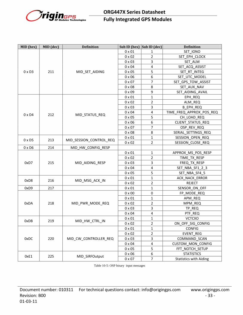
OSP Binary Input Messages
MID (hex) MID (dec) Definition Sub ID (hex) Sub ID (dec) Definition
0 x 35 53 Advanced Power Management
0 x 80 128 Initialize Data Source
0 x 81 129 Switch to NMEA Protocol
0 x 82 130 Set Almanac (upload)
0 x 84 132 Software Version (Poll)
0 x 86 134 Set Main Serial Port
0 x 87 135 Switch Protocol
0 x 88 136 Mode Control
0 x 89 137 DOP Mask
0 x 8A 138 MID_SET_DGPS_MODE
0 x 8B 139 Elevation Mask
0 x 8C 140 Power Mask
0 x 8D 141 Editing Residual
0 x 8E 142 Steady-State Detection
0 x 8F 143 Static Navigation
0 x 90 144 Poll Clock Status
0 x 92 146 Poll Almanac
0 x 93 147 Poll Ephemeris
0 x 95 149 Set Ephemeris (upload)
0 x 96 150 Switch Operating Mode
0 x 97 151 Set Trickle Power Parameters
0 x 98 152 Poll Navigation Parameters
0 x A5 165 Set UART Configuration
0 x A6 166 Set Message Rate
0 x A7 167 Low Power Acquisition Parameters
0 x A8 168 MID_POLL_CMD_PARAM
0 x A9 169 Set Datum
0 x AA 170 Set SBAS Parameters
0 x AC 172 MID_DrIn
0 x 01 1 Set DrNavInit
0 x 02 2 Set DrNavMode
0 x 03 3 Set GyrFactCal
0 x 04 4 Set DrSensParam
0 x 05 5 Poll DrValid
0 x 06 6 Poll GyrFactCal
0 x 07 7 Poll DrSensParam
0 x 13 19 DR Debug Information
0 x AF 175 Send Command String
0 x B2 178 SIRF_MSG_SSB_TRACKER_IC
0 x 14 20 Patch Storage Control
0 x 22 34 Patch Memory Load Request
0 x 26 38 Patch Memory Exit Request
0 x 28 40 Patch Memory Start Request
0 x 90 144 Patch Manager Prompt
0 x 91 145 Patch Manager Ack.
0 x CD 205 Set Generic Software Control 0 x 10 16 Software Commanded OFF
0 x D1 209 MID_QUERY_REQ
0 x D2 210 MID_POS_REQ
Table 10-5: OSP binary input messages
ORG447X Series Datasheet
Fully Integrated GPS Modules
Document number: 010311 For technical questions contact: [email protected] www.origingps.com Revision: B00 01-03-11
- 33 -
MID (hex) MID (dec) Definition Sub ID (hex) Sub ID (dec) Definition
0 x D3 211 MID_SET_AIDING
0 x 01 1 SET_IONO
0 x 02 2 SET_EPH_CLOCK
0 x 03 3 SET_ALM
0 x 04 4 SET_ACQ_ASSIST
0 x 05 5 SET_RT_INTEG
0 x 06 6 SET_UTC_MODEL
0 x 07 7 SET_GPS_TOW_ASSIST
0 x 08 8 SET_AUX_NAV
0 x 09 9 SET_AIDING_AVAIL
0 x D4 212 MID_STATUS_REQ
0 x 01 1 EPH_REQ
0 x 02 2 ALM_REQ
0 x 03 3 B_EPH_REQ
0 x 04 4 TIME_FREQ_APPROX_POS_REQ
0 x 05 5 CH_LOAD_REQ
0 x 06 6 CLIENT_STATUS_REQ
0 x 07 7 OSP_REV_REQ
0 x 08 8 SERIAL_SETTINGS_REQ
0 x D5 213 MID_SESSION_CONTROL_REQ 0 x 01 1 SESSION_OPEN_REQ
0 x 02 2 SESSION_CLOSE_REQ
0 x D6 214 MID_HW_CONFIG_RESP
0xD7 215 MID_AIDING_RESP
0 x 01 1 APPROX_MS_POS_RESP
0 x 02 2 TIME_TX_RESP
0 x 03 3 FREQ_TX_RESP
0 x 04 4 SET_NBA_SF1_2_3
0 x 05 5 SET_NBA_SF4_5
0xD8 216 MID_MSG_ACK_IN 0 x 01 1 ACK_NACK_ERROR
0 x 02 2 REJECT
0xD9 217 0 x 01 1 SENSOR_ON_OFF
0xDA 218 MID_PWR_MODE_REQ
0 x 00 0 FP_MODE_REQ
0 x 01 1 APM_REQ
0 x 02 2 MPM_REQ
0 x 03 3 TP_REQ
0 x 04 4 PTF_REQ
0xDB 219 MID_HW_CTRL_IN 0 x 01 1 VCTCXO
0 x 02 2 ON_OFF_SIG_CONFIG
0xDC 220 MID_CW_CONTROLLER_REQ
0 x 01 1 CONFIG
0 x 02 2 EVENT_REG
0 x 03 3 COMMAND_SCAN
0 x 04 4 CUSTOM_MON_CONFIG
0 x 05 5 FFT_NOTCH_SETUP
0xE1 225 MID_SiRFOutput 0 x 06 6 STATISTICS
0 x 07 7 Statistics with Aiding
Table 10-5: OSP binary input messages
ORG447X Series Datasheet
Fully Integrated GPS Modules
Document number: 010311 For technical questions contact: [email protected] www.origingps.com Revision: B00 01-03-11
- 34 -
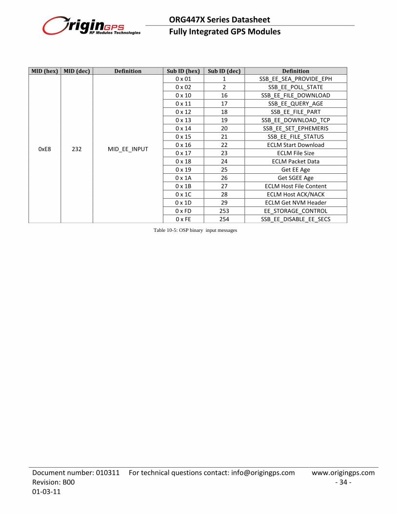
Table 10-5: OSP binary input messages
MID (hex) MID (dec) Definition Sub ID (hex) Sub ID (dec) Definition
0xE8 232 MID_EE_INPUT
0 x 01 1 SSB_EE_SEA_PROVIDE_EPH
0 x 02 2 SSB_EE_POLL_STATE
0 x 10 16 SSB_EE_FILE_DOWNLOAD
0 x 11 17 SSB_EE_QUERY_AGE
0 x 12 18 SSB_EE_FILE_PART
0 x 13 19 SSB_EE_DOWNLOAD_TCP
0 x 14 20 SSB_EE_SET_EPHEMERIS
0 x 15 21 SSB_EE_FILE_STATUS
0 x 16 22 ECLM Start Download
0 x 17 23 ECLM File Size
0 x 18 24 ECLM Packet Data
0 x 19 25 Get EE Age
0 x 1A 26 Get SGEE Age
0 x 1B 27 ECLM Host File Content
0 x 1C 28 ECLM Host ACK/NACK
0 x 1D 29 ECLM Get NVM Header
0 x FD 253 EE_STORAGE_CONTROL
0 x FE 254 SSB_EE_DISABLE_EE_SECS

ORG447X Series Datasheet
Fully Integrated GPS Modules
Document number: 010311 For technical questions contact: [email protected] www.origingps.com Revision: B00 01-03-11
- 35 -
11. Handling Information
11.1. Product Packaging and Delivery
Figure 11-1: Carrier
Carrier material: Conductive Polystyrene
Pad 1 position
FEED DIRECTION
TOP VIEW

ORG447X Series Datasheet
Fully Integrated GPS Modules
Document number: 010311 For technical questions contact: [email protected] www.origingps.com Revision: B00 01-03-11
- 36 -
Figure 11-2: Module position
Figure 11-3: Reel
Reel material: Antistatic Plastic
Each reel contains 200, 500, 1000, 1500 or 2000 modules.

ORG447X Series Datasheet
Fully Integrated GPS Modules
Document number: 010311 For technical questions contact: [email protected] www.origingps.com Revision: B00 01-03-11
- 37 -
11.2. Moisture Sensitivity The devices are moisture sensitive at MSL 3 according to standard IPC/JEDEC J-STD-033B.
The recommended drying process for samples and bulk components is to be done at 125°C for 48 hours.
11.3. Assembly The ORG447X series module support automatic assembly and reflow soldering processes on
the component side of the motherboard PCB according to standard IPC/JEDEC J-STD-020D for
LGA SMD. Suggested solder paste stencil is 5 mil to ensure sufficient solder volume.
Figure 11-4: Recommended soldering profile
Suggested peak reflow temperature is 250°C for 10 sec. for Pb-Free solder paste.
Absolute Maximum reflow temperature is 260°C for 10 sec.
11.4. Rework If localized heating is required to rework or repair the ORG447X series module, precautionary
methods are required to avoid exposure to solder reflow temperatures that can result in
permanent damage to the device.
11.5. ESD Sensitivity The ORG447X series module is ESD sensitive device and should be handled with care.

ORG447X Series Datasheet
Fully Integrated GPS Modules
Document number: 010311 For technical questions contact: [email protected] www.origingps.com Revision: B00 01-03-11
- 38 -
11.6. Compliances The following standards are applied on the ORG447X series modules production:
IPC-6011/6012 Class2 for PCB manufacturing
IPC-A-600 Class2 for PCB inspection
IPC-A-610D Class2 for SMT acceptability
The ORG447X series modules are being manufactured ISO 9001:2000 accredited facilities.
The ORG447X series modules are designed and being manufactured and handled to
comply with and according with Pb-Free/RoHS Directive 2002/95/EC on the restriction
of the use of certain hazardous substances in electrical and electronic equipment.
The ORG447X series modules comply with the following EMC standards:
EU CE EN55022:06+A1(07), Class B
US FCC 47CFR Part 15:09, Subpart B, Class B
11.7. Safety Information Improper handling and use can cause permanent damage to the device.
There is also the possible risk of personal injury from mechanical trauma or shocking hazard.
11.8. Disposal Information The product should not be treated as household waste.
For more detailed information about recycling electronic components, please contact your local
waste management authority.
ORG447X Series Datasheet
Fully Integrated GPS Modules
Document number: 010311 For technical questions contact: [email protected] www.origingps.com Revision: B00 01-03-11
- 39 -
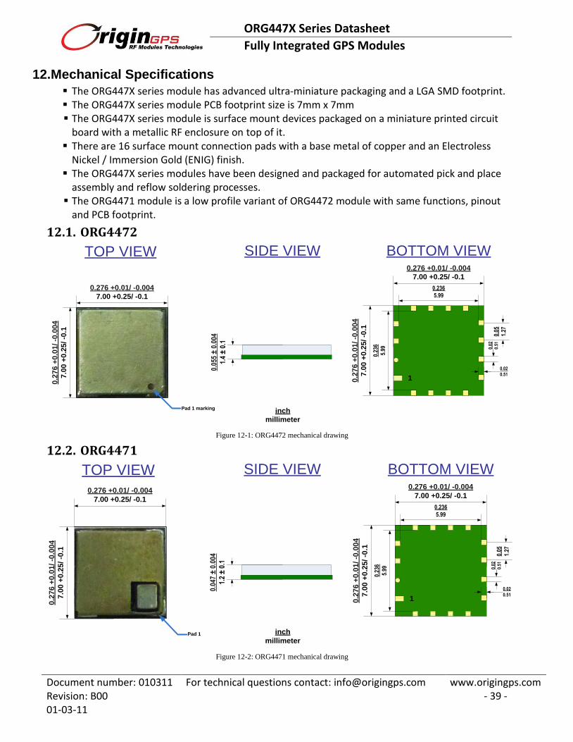
12. Mechanical Specifications
The ORG447X series module has advanced ultra-miniature packaging and a LGA SMD footprint. The ORG447X series module PCB footprint size is 7mm x 7mm The ORG447X series module is surface mount devices packaged on a miniature printed circuit
board with a metallic RF enclosure on top of it. There are 16 surface mount connection pads with a base metal of copper and an Electroless
Nickel / Immersion Gold (ENIG) finish. The ORG447X series modules have been designed and packaged for automated pick and place
assembly and reflow soldering processes. The ORG4471 module is a low profile variant of ORG4472 module with same functions, pinout
and PCB footprint.
12.1. ORG4472
TOP VIEW BOTTOM VIEW
1
SIDE VIEW0.276 +0.01/ -0.004
7.00 +0.25/ -0.1
0.2
76
+0.0
1/ -0
.00
4
7.0
0 +
0.2
5/ -0
.1
inch
millimeter
0.2
76
+0
.01
/ -0
.00
4
7.0
0 +
0.2
5/ -0
.1
0.276 +0.01/ -0.004
7.00 +0.25/ -0.1
0.05
5 ±
0.0
04
1.4
± 0
.1
0.02
0.51
0.02
0.51
0.05
1.27
0.236
5.99
0.23
6
5.99
Pad 1 marking
Figure 12-1: ORG4472 mechanical drawing
12.2. ORG4471
TOP VIEW BOTTOM VIEW
1
SIDE VIEW0.276 +0.01/ -0.004
7.00 +0.25/ -0.1
0.2
76
+0.0
1/ -0
.00
4
7.0
0 +
0.2
5/ -0
.1
inch
millimeter
0.2
76
+0
.01
/ -0
.00
4
7.0
0 +
0.2
5/ -0
.1
0.276 +0.01/ -0.004
7.00 +0.25/ -0.1
0.04
7 ±
0.0
04
1.2
± 0
.1
0.02
0.51
0.02
0.51
0.05
1.27
0.236
5.99
0.23
6
5.99
Pad 1
Figure 12-2: ORG4471 mechanical drawing
ORG447X Series Datasheet
Fully Integrated GPS Modules
Document number: 010311 For technical questions contact: [email protected] www.origingps.com Revision: B00 01-03-11
- 40 -
Dimensions Length Width Height
Weight ORG4471 ORG4472
mm 7.0 +0.25/ -0.1 7.0 +0.25/ -0.1 1.2 ± 0.1 1.4 ± 0.1 gr 0.3
inch 0.276 +0.01/ -0.004 0.276 +0.01/ -0.004 0.047 ± 0.004 0.055 ± 0.004 oz 0.05
Table 12-1: ORG447X series mechanical summary
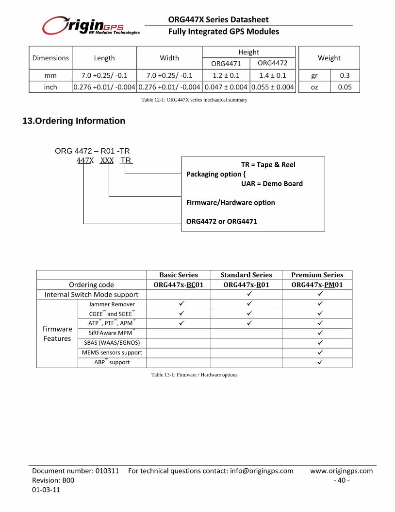
13. Ordering Information
ORG 4472 – R01 -TR
447X XXX TR
Table 13-1: Firmware / Hardware options
Basic Series Standard Series Premium Series
Ordering code ORG447x-BC01 ORG447x-R01 ORG447x-PM01
Internal Switch Mode support
Firmware Features
Jammer Remover CGEE
™ and SGEE
™
ATP™
, PTF™
, APM™
SiRFAware MPM
™
SBAS (WAAS/EGNOS) MEMS sensors support
ABP™
support
TR = Tape & Reel Packaging option
UAR = Demo Board Firmware/Hardware option ORG4472 or ORG4471