Embed Size (px)
Citation preview
FAKULTÄT FÜR ELEKTROTECHNIK UND INFORMATIONSTECHNIK, LEHRSTUHL FÜR
NANOELEKTRONIK, TECHNISCHE UNIVERSITÄT MÜNCHEN
FUNCTIONALIZATION OF
SURFACES FOR
SENSORS AND OPTOELECTRONICS
ALINA LYULEEVA
Vollständiger Abdruck der von der Fakultät für Elektrotechnik und Informationstechnik der
Technischen Universität München zur Erlangung des akademischen Grades eines
Doktors der Naturwissenschaften (Dr.rer.nat.)
genehmigten Dissertation.
Vorsitzende/r: Prof. Dr. Oliver Hayden
Prüfende/-r der Dissertation:
1. Prof. Dr. Paolo Lugli
2. Prof. Dr. Dr. h. c. Bernhard Rieger
3. Prof. Dr. Marc Tornow
Die Dissertation wurde am 10. Januar 2018 bei der Technischen Universität München
eingereicht und durch die Fakultät für Elektrotechnik und Informationstechnik am 5. April
2018 angenommen.


To my family
Посвещается моей семье
Meiner Familie gewidmet

4
“Life is like mountains:
When it happens that you reach a valley,
Watch out for another peak to conquer!”
Vladimir Yurievich Kusov
(Владимир Юрьевич Кусов)
- Just ignore the trees and the clouds, then you will see the stars -
5
Acknowledgements
I would like to thank Prof. Dr. Lugli (University of Bozen-Bolzano, Italy) for being my
Dissertation supervisor and for providing the opportunity to work in his group. Already after
two weeks of my scientific work, he allowed me to develop a completely new project in the field
of a hitherto unknown material. With his confidence in my independent work, I had the
freedom to explore different subjects. I chose two-dimensional materials out of personal
interest. However, this subject grew rapidly into my new field of expertise. Additionally, many
thanks to the Nano-group and especially the group members Marco Bobinger, Florin Loghin,
Andreas Albrecht, Vijay Bhatt (TUM, Chair of Nanoelectronics, Munich) and Dr. Aniello
Falco (University of Bozen-Bolzano, Italy). Many thanks to Katharina Melzer and Dr. Frank
Deubel, who have advised me especially in the beginning of my work.
Thanks to the Alberta/Technical University of Munich (UofA/TUM) International Gradate
School for Hybrid Functional Materials (ATUMS) for its existence and for the opportunity to
be part of its development from the very beginning. Many thanks to Prof. Dr. Dr. h.c.
Bernhard Rieger (TUM, Chair of Macromolecular Chemistry, Munich) and Prof. Jonathan
Veinot (UofA, Chemistry Department, Edmonton, Canada), who are the ATUMS German and
Canadian Program Directors, respectively. With their help I was able to engage with my
Canada- and Germany-based colleagues and initiate collaborative projects, which led to
several joint-, first and also second author publications. With that, also many thanks to the
whole ATUMS community. In my opinion, it is a special program which is led by very
interesting, creative and simply nice people. Thank you guys for the opportunity to be a part
of this!
Huge appreciation to the group of Prof. Frank Hegmann (UofA, Physics Department,
Edmonton, Canada) and of course to Frank himself, who hosted me during my research stays
in Canada. Being my second supervisor, he advised me a lot not only in my scientific work, but
also in my future career plans and even sometimes karaoke singing!
Many thanks to Prof. Dr.-Ing. Markus Becherer (TUM, Chair of Nanoelectronics, Munich),
who has taken over the supervision during my last year of the PhD. He was a great support in
scientific discussions, projects and collaborations management and paper writing. Also Dr.
Almudena Rivadeneyra’s (TUM, Chair of Nanoelectronics, Munich) help is highly
appreciated. She not only introduced me into the humidity sensor field, but also helped with
advice for my first independent steps in science.

6
Many thanks to my collaboration partners Marc Kloberg, Philipp Holzmüller and Mary A.
Narreto. Thank you guys for fruitful discussions and exciting research. It was great fun to work
with you and see how ideas become reality.
Dr. Tobias Helbich, I thank you for this pleasure to already here and now write “Dr.” in front
of your name. It was a great honour and lots of fun to walk through all these 9 years of studies
at TUM, side-by-side with you. – “komm zurück… pffff!” Also many thanks to my friends from
Munich, Scheeßel and St.Petersburg! Without having you and your support, the whole
painting would have lost its colors.
Great appreciation to everyone, who helped me to find all the little and not so little mistakes
in my thesis!
Great thanks to Prof. Martin Stutzmann (TUM, Walter-Schottky Institute, Munich), who
always offered his support and advice. Being not only a great professor, he also helped a lot
with advice, due to his massive knowledge background in two-dimensional systems.
Of course, not to forget: huge thanks and great appreciation to Prof. Sir Kostya Novoselov
(University of Manchester, UK). Thank you very much for your honesty, hours of discussion,
very helpful consulting, guidance during my PhD and advice for my future career plans!
And last but definitely not least: I want to give heartfelt thanks to my whole family in
St.Petersburg, Hamburg-Area and Frankfurt(-Area). Especially my grandparents Margarita
Fyodorovna Kusova and Vladimir Yurievich Kusov, my mother Irina Vladimirovna
Adam and my sister Yuliana Maksimovna Lyuleeva together with my little niece Lara
Schöfer! I am very lucky to have had your support day and night, either spring, summer,
autumn or winter, even if it was just a simple hello on the phone.
Thank you all!
7
1 CONTENTS
Table of Abbreviations ............................................................................................................................ 9
1. Nanomaterials and their Surface Engineering .............................................................................. 15
1.1. Control of the Properties of Nanomaterials via Surface Functionalization .......................... 15
1.1.1. Non-covalent Surface Modification .............................................................................. 18
1.1.2. Covalent Surface Modification ...................................................................................... 20
1.2. The Rise of 2D Silicon Nanomaterials: Silicene & Silicane .................................................... 24
1.2.1. Silicene – From Synthesis to Application ...................................................................... 24
1.2.2. Silicane – Hydrogenated Silicon Monolayer as a Novel Representative of an
sp3-Hybridized Freestanding 2D Silicon ........................................................................................ 26
2. Methods and Fabrication Techniques .......................................................................................... 29
2.1. General Information ............................................................................................................. 29
2.2. Synthesis and Functionalization of SiNSs .............................................................................. 29
2.2.1. Synthesis of Silicane ...................................................................................................... 29
2.2.2. Etching of Silicon Nanosheets(Helbich, Lyuleeva, Höhlein, et al. 2016) ....................... 29
2.2.3. Functionalization of SiNSs in the Microwave-reactor System ...................................... 30
2.2.4. Functionalization of SiNS for humidity sensors: ........................................................... 30
2.2.5. Hydrolyzation reaction of tBMA functional groups for humidity sensor ...................... 30
2.2.6. AIBN-based radical-induced functionalization of SiNSs with substrate and
polymerization .............................................................................................................................. 31
2.3. Photolithography and Metal Evaporation for Interdigital (IDE) Structure Patterning ......... 31
2.4. SGFET Fabrication and Characterization ............................................................................... 33
2.4.1. SGFET fabrication: ......................................................................................................... 33
2.4.2. Electrical Characterization ............................................................................................ 34
2.4.3. Electron Paramagnetic Resonance (EPR) studies.......................................................... 35
2.5. Humidity sensor fabrication .................................................................................................. 35
2.5.1. Device Fabrication ......................................................................................................... 35
2.5.2. Device Characterization ................................................................................................ 36
2.6. Photonic Sensor Fabrication ................................................................................................. 36
2.6.1. Compounding of the SiNS-substrate@polymer Composites ........................................ 36
2.6.2. Electrical Device Characterization ................................................................................. 36
2.7. Material preparation for the TIPL and TRPL measurements ................................................ 37
2.7.1. Measurements in solution ............................................................................................ 37
2.7.2. Measurements in solid state ......................................................................................... 37
2.8. TIPL and TRPL measurements ............................................................................................... 37
8
2.9. Transmittance measurements .............................................................................................. 38
3. Results and Discussion .................................................................................................................. 39
3.1. Synthesis, Functionalization and Characterization ............................................................... 39
3.2. PL and Time-resolved PL Studies of Hydrogenated and Functionalized SiNSs. .................... 43
4. Application of SiNSs in Nanoelectronics ....................................................................................... 53
4.1. Modified Silicon Nanosheets based Solution-gated Field-effect Transistor (SGFET) ........... 53
4.1.1. State of the Art and Aim ............................................................................................... 54
4.1.2. Results and Discussion .................................................................................................. 55
4.1.3. Summary ....................................................................................................................... 64
4.2. SiNS-Polystyrene@Polystyrene Multifunctional Composite for Photonic Sensor................ 65
4.2.1. State of the Art and Aim ............................................................................................... 66
4.2.2. Results and Discussion .................................................................................................. 67
4.2.3. Summary ....................................................................................................................... 74
4.3. Tuning the Hydrophilicity of SiNSs Surface for Capacitive Humidity Sensor Fabrication ..... 76
4.3.1. State of the Art and Aim ............................................................................................... 77
4.3.2. Results and Discussion .................................................................................................. 79
4.3.3. Summary ....................................................................................................................... 87
5. Summary and Outlook .................................................................................................................. 88
6. Publications ................................................................................................................................. 115
7. References .................................................................................................................................... 92
8. Appendix ..................................................................................................................................... 118
8.1. Online Article: Silicon Nanosheets. New Materials for Future Applications (Lyuleeva,
Helbich, Lugli, et al. 2017) ............................................................................................................... 118
8.2. TRPL Measurements: .......................................................................................................... 119
8.2.1. PL and TRPL Measurements of SiNS-Dodecene/P3HT blends .................................... 121
8.2.2. PL and TRPL Measurements of SiNS-PhAc/P3HT blends ............................................ 123
8.2.3. PL and TRPL Measurements of SiNS-ThAc/P3HT blends ............................................ 125
8.3. LEPR Measurements: .......................................................................................................... 127
8.4. Grazing-Incidence Wide-Angle X-ray Scattering (GIWAXS) Measurements ....................... 131
8.5. SiNS-substrate and SiNS-polymer@polymer Quantum Yields ........................................... 134
8.6. Cover Pages ......................................................................................................................... 136
8.6.1. Nanocomposites: One-Step Synthesis of Photoluminescent Covalent Polymeric
Nanocomposites from 2D Silicon Nanosheets (Adv. Funct. Mater. 37/2016) ............................ 136
8.6.2. Silicon Nanosheets: Lewis Acid Induced Functionalization of Photoluminescent 2D
Silicon Nanosheets for the Fabrication of Functional Hybrid Films (Adv. Funct. Mater. 21/2017)
137
9. Licenses for Copyright Content ................................................................................................... 138
9
TABLE OF ABBREVIATIONS
0D zero-dimensional
1D one-dimensional
2D two-dimensional
AFM atomic force microscopy
DFT density functional theory
EDX x-ray spectroscopy
EPR electron paramagnetic resonance
FET field-effect transistors
FTIR Fourier transform infrared spectroscopy
hBN hexagonal boron nitride
LED light emitting diode
MMA methacrylic acid
MW microwave
OSiNS oxidized silicon nanosheets
PS polystyrene
PAA poly(acrylic acid)
PMMA poly(methacrylic acid)
RH relative humidity
SEM scanning tunneling microscopy
SiNS silicon nanosheets
SiNC silicon nanocrystals
SiNW silicon nanowires
tBMA tert-butyl methacrylate
TMDC transition metal dichalcogenide
XPS x-ray photoelectron spectroscopy

10

11
INTRODUCTION AND OUTLINE
ENGLISH
With the potential to overcome barriers in current silicon-based semiconductor technology, two-
dimensional (2D) materials is a rapidly developing field in nano-scale applied sciences. This
dissertation provides guidance for the fabrication and application of functionalized 2D silicon
nanosheets (SiNSs), which show remarkable (opto)electronic properties. Their incorporation into well-
known fabrication techniques leads to highly sensitive solution-gated field-effect transistors,
photodetectors and humidity sensors.
Among 2D materials, graphene was the first one to be successfully characterized by Novoselov et al.
in 2004. Following this, the synthesis and possible application of 2D silicon became a more central
concern than has hitherto been the case. Silicon in its 2D configuration is believed to exhibit
outstanding (opto)electronic properties. Some few examples are the consistent green
photoluminescence, the possibility of band gap opening and its semiconducting behavior. The
thickness of the layered material is only a few nanometers, but at the same time lateral sizes can go
up to micro dimensions. Both 2D silicon configurations and the development in the field of
nanomaterials are presented in the first chapter.
This work presents also guidance for the fabrication of nano-devices based on novel hybrid materials.
Starting from the fundamental understanding of the physics of the discovered material, it is also
explained how to control its properties for further use. With the SiNSs as an example, precise
engineering of the surface with the help of radical hydrosilylation reactions is introduced. This surface
modification was carried out to perform covalent functionalization, which enables the protection and
stabilization of the sheets against damage from UV light and oxygen exposure. Consequently, this
simple step increases the lifetime of the SiNSs and provides a facile integration of the modified
material into well-known deposition techniques. This work has been carried out in close collaboration
with the groups of the Alberta/Technical University of Munich (UofA/TUM) International Gradate
School for Hybrid Functional Materials (ATUMS). Especially the synthesis and the surface modification
of the herein used material has been mainly carried out by Dr. Tobias Helbich and his students from
the Chemistry Department of the TU Munich.
As a result of this surface modification, an established way towards the fabrication of novel devices
could be guaranteed at the chair of Nanoelectronics (TU Munich). These fabrication techniques are
presented and explained in more detail in chapter 4. The first application is the fabrication of improved
SiNS-substrate/P3HT based solution-gated field-effect transistors. These transistors show increased
12
sensitivity with higher transconductance and ON/OFF ratios. The second presented application is a
prototype of a highly sensitive photonic sensor (chapter 4.2.). SiNS-polystere@polysterene composite
has been synthesized and integrated into the device as a light sensitive material for that purpose.
Finally, a capacitive humidity sensor is being developed (chapter 4.3.) which shows the first steps
towards response to surrounding molecules and conditions such as water at certain temperatures.
The broad range of the predicted application areas comprises diverse nanoelectronic devices, sensors
and lithium-ion batteries based on monolayer silicon nanomaterials.
GERMAN
Die Suche nach neuen Möglichkeiten aktuelle Grenzen der Si-Halbleitertechnologien zu überwinden,
treibt in den nanobasierten angewandten Wissenschaften die Forschung der zweidimensionalen (2D)
Materialien voran. Diese Dissertation bietet eine Orientierungshilfe für die Herstellung und
Anwendung von funktionalisierten 2D-Silciumnanoschichten (SiNSs), die bemerkenswerte
(opto)elektronische Eigenschaften aufweisen. Ihr Einbau in konventionelle Technologien führt zur
Herstellung von hochsensitiven Feldeffekt-Transistoren, sowie Licht- und Feuchtigkeitssensoren.
Im Bereich der 2D Materialien war Graphen der Vorreiter, nachdem es von Novoselov et al. in 2004
erfolgreich charakterisiert wurde. Daraus resultierend bekam stärker als bisher die Synthese und die
mögliche Anwendung von 2D Silicium ein zentrales Anliegen. Es wird erwartet, dass Silicium in seiner
2D Konfiguration außergewöhnliche Eigenschaften aufweist. Einige Beispiele sind die konsistente
grüne Photolumineszenz, die Möglichkeit die Bandlücke des Materials zu öffnen und sein Verhalten
als Halbleiter. Die Schichtdicke des Materials ist nur einige Nanometer groß, wobei die lateralen
Dimensionen bis zu einer Größe von einigen Mikrometern reichen. Beide Formen des 2D Siliciums und
die Entwicklung im Bereich der Nanomaterialien sind im ersten Kapitel im Detail beschrieben.
Diese Arbeit bietet ebenso eine Anleitung für die Anfertigung von Nanogeräten, welche auf neuartigen
Hybridmaterialien basieren. Angefangen mit dem grundlegenden Verständnis der Physik des
entdeckten Materials, wird im Folgenden auch erklärt, wie dessen Eigenschaften für weiterführende
Nutzung kontrolliert werden können. Mit den SiNSs als Beispiel wird das präzise Engineering der
Oberflächen mit Hilfe von radikalischer Hydrosilylierungsreaktionen vorgestellt. Diese
Oberflächenmodifizierung wurde mit Hilfe von kovalenten Funktionalisierungsreaktionen ermöglicht,
die den Schutz und die Stabilisierung der Nanoschichten gegen Zerstörung durch UV-Licht und
Sauerstoff Exposition bieten. Als Resultat verlängert dieser einfache Schritt die Lebensdauer der SiNSs
und bietet eine mühelose Integration des modifizierten Materials in bereits bekannte

13
Depositionstechniken. Dieser Teil der Arbeit entstand in enger Kollaboration mit den Gruppen des
Internationalen Graduiertenkollegs „Alberta/Technical University of Munich Graduate School for
Functional Hybrid Materials“ (ATUMS, International Research Training Group, IRTG 2022).
Insbesondere die Synthese und die Oberflächenmodifizierung des hierbei eingesetzten Materials
wurde durch Dr. Tobias Helbich und seine Studenten an der Fakultät für Chemie der TU München
durchgeführt.
Ausgehend von der präzisen Oberflächenmodifizierung wurde eine bewehrte Methode für die
Herstellung von neuartigen Geräten am Lehrstuhl für Nanoelektronik (TU München) erarbeitet und
vorgestellt. Diese Anwendungsmethoden werden im Kapitel 4 im Detail erläutert. Die erste
Anwendung stellt die Herstellung von verbesserten SiNS-Substrat/P3HT basierten
Feldeffekttransistoren dar. Sie zeigen angestiegene Sensitivität mit einem höheren Gegenwirkleitwert
und AN/AUS Verhältnis. Die zweite hierbei vorgestellte Anwendung (Kapitel 4.2.) ist der Prototyp eines
sensitiven photonischen Sensors. Dafür wurde das Verbundmaterial SiNS-Polystyrol/Polystyrol
synthetisiert und in das Gerät als lichtsensitives Material integriert. Zu guter Letzt wurde ein
kapazitiver Feuchtigkeitssensor entwickelt (Kapitel 4.3.), der die ersten Schritte in Richtung
sensorischer Rückmeldung auf umgebende Moleküle und Bedingungen wie Wasser in der Atmosphäre
bei verschiedenen Temperaturen zeigt.
Auf Basis von Silicium-Einzelschichten wurde eine große Auswahl an Anwendungsbereichen
vorhergesagt, welche unter Anderem diverse nanoelektronische Geräte, Sensoren und Lithium-Ionen-
Batterien umfassen.

14
15
1. NANOMATERIALS AND THEIR SURFACE ENGINEERING
1.1. CONTROL OF THE PROPERTIES OF NANOMATERIALS VIA SURFACE FUNCTIONALIZATION Functional nanomaterial-based sensors are widely used in medical and industrial applications. New
properties can arise with lowering the dimensionality of the material. A few examples include:
quantum confinement (Brus 1994; Wilcoxon et al. 1999), band gap opening (Balendhran et al. 2015),
conductivity with ideal electronic and transport properties (Oscar D. Restrepo, Krymowski, et al. 2014)
and photoluminescence (PL). (Jiang et al. 2015) For successful applications, however, the devices
typically require surfaces that are durable, highly sensitive, cheap and biocompatible. Varying
morphology (Sukhanova et al. 2011), chemical reactivity (Gatoo et al. 2014), band gap tuning
(Brennan, Morishita & Michelle J. S. Spencer 2016) and charge transport (McNeil et al. 2012;
Skrypnychuk et al. 2015) on the interface between different materials in a composite can be exploited
for new device engineering at the nanoscale. A general overview of low-dimensional materials
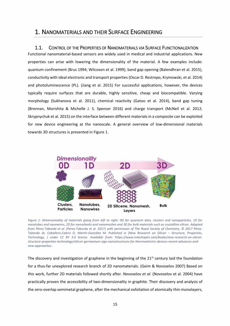
towards 3D structures is presented in Figure 1.
Figure 1: Dimensionality of materials going from left to right: 0D for quantum dots, clusters and nanoparticles, 1D for nanotubes and nanowires, 2D for nanosheets and nanomeshes and 3D for bulk materials such as crystalline silicon. Adapted from Pérez-Taborda et al. (Perez-Taborda et al. 2017) with permission of The Royal Society of Chemistry, © 2017 Pérez‐Taborda JA, Caballero-Calero O, Martín‐González M. Published in [New Research on Silicon – Structure, Properties, Technology, ] under CC BY 3.0 license. Available from: https://www.intechopen.com/books/new-research-on-silicon-structure-properties-technology/silicon-germanium-sige-nanostructures-for-thermoelectric-devices-recent-advances-and-new-approaches.
The discovery and investigation of graphene in the beginning of the 21st century laid the foundation
for a thus-far unexplored research branch of 2D nanomaterials. (Geim & Novoselov 2007) Based on
this work, further 2D materials followed shortly after. Novoselov et al. (Novoselov et al. 2004) have
practically proven the accessibility of two-dimensionality in graphite. Their discovery and analysis of
the zero-overlap semimetal graphene, after the mechanical exfoliation of atomically thin monolayers,
16
has evoked an explosive amount of work worldwide. Until now, the main purpose was not only finding
further analogues of graphene, but also on understanding its fundamental properties to finally pave
the way towards applied science. (Arivalagan et al. 2011) This prompted researchers in the fields of
materials science, physics and chemistry, which deal with the interface phenomena (for example
charge transfer, or molecular interaction), to start searching for new insights in the 2D nanomaterials
world. The applied physics and (electro)engineering fields also rapidly discovered potential in the use
of these materials for innovative technologies. 2D materials might help overcome the present
challenges (e.g., band gap control and ease of manufacturing) and fulfil the desired goals (e.g.,
reduction of power consumption and semiconductor scaling (Kim et al. 2003; Handy 2014)) in today’s
applications.
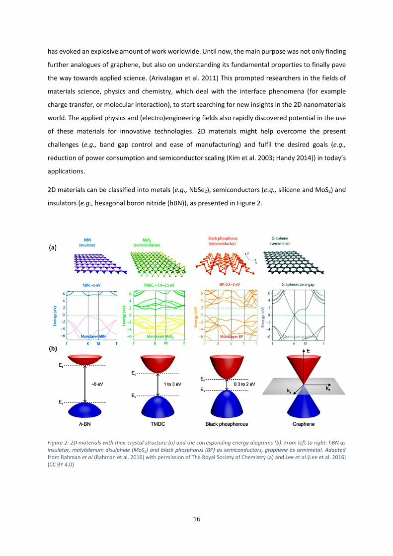
2D materials can be classified into metals (e.g., NbSe2), semiconductors (e.g., silicene and MoS2) and
insulators (e.g., hexagonal boron nitride (hBN)), as presented in Figure 2.
Figure 2: 2D materials with their crystal structure (a) and the corresponding energy diagrams (b). From left to right: hBN as insulator, molybdenum disulphide (MoS2) and black phosphorus (BP) as semiconductors, graphene as semimetal. Adapted from Rahman et al.(Rahman et al. 2016) with permission of The Royal Society of Chemistry (a) and Lee et al.(Lee et al. 2016) (CC BY 4.0)
17
Elemental analogues such as germanene and stanene have already been discovered, studied and
successfully presented (Balendhran et al. 2015), as well as heterostructures such as transition metal
dichalcogenides (TMDCs) with the formula MX2 (e.g., WTe2, MoS2, MoSe2) (Wilson, J. A.; Yoffe 1969;
Velusamy et al. 2015) which have attracted interest due to their outstanding electronic, optical,
mechanical and chemical properties. (Wilson, J. A.; Yoffe 1969; Yoffe 1993)
Silicon, as one of the group IV family members, has also 2D representatives: silicene as an analogue to
graphene (Vogt et al. 2012; Chiappe et al. 2012; Liu et al. 2013; Xu et al. 2012; Tao et al. 2015; Aufray
et al. 2010); silicane, which is a hydrogenated silicon monolayer (Hussain et al. 2013) and siloxene with
-OH and -H surface termination. (Dahn et al. 1993) Silicene has attracted attention already in 1994
(Takeda & Shiraishi 1994), when it was theoretically explored by Takeda and Shiraishi et al. This nearly
planar material with a honeycomb lattice configuration shows structural and electronic properties
which are comparable to those of graphene. (Zhao et al. 2016) Nevertheless, due to its
sp2-hybridization, it suffers from the same disadvantage as graphene: the difficulty of stable and
irreversible functionalization. This modification step would also allow a controlled opening of the band
gap without the destruction of material’s surface, which would allow the controlled opening of the
band gap. Both, covalent (Bekyarova et al. 2009; Elias et al. 2009) and non-covalent (Wang & Hersam
2011; Chen et al. 2007; Wang & Hersam 2009) functionalizations of planar graphene have been
investigated in detail for precise shift of its Fermi level (Lomeda et al. 2008) for the desired need in
applications.
Silicene is also governed by sp2-hybridization, which makes the treatment of this nanomaterial
difficult. Furthermore, in conflict with the outstanding features of 2D silicon (vide supra) and due to
its puckered and crinkled structure (Brumfiel 2013; Merali 2013), silicene is rather unstable in ambient
conditions and needs to be protected from UV light and oxygen. (G. Liu et al. 2014; Helbich, Lyuleeva,
Höhlein, et al. 2016; Helbich, Lyuleeva, Ludwig, et al. 2016) As soon as this material is exposed to air
and light, it starts to degrade, forming SiOx (x = 1,2), which is an insulating material. Nevertheless,
despite these difficulties, Akinwande et al. succeeded in 2015 in building a silicene based field-effect
transistor (FET), which was operating even at room-temperature. (Tao et al. 2015) For the first time,
it was experimentally proven that silicene exhibits the predicted ambipolar Dirac charge transport
(Scalise et al. 2014; Cahangirov et al. 2009; Liu et al. 2011) and a room-temperature mobility of about
100 cm2V-1s-1 attributed to acoustic phonon-limited transport (X. Li et al. 2013) and grain boundary
scattering. However, in general, most of the elemental analogues of graphene, such as germanene
(Cahangirov et al. 2009; Liu et al. 2011; Ni et al. 2012), phosphorene (Guo et al. 2016; H. Liu et al.
2014), and silicene need to be encapsulated with additional molecules or materials, which requires an
additional fabrication step.
18
Still, due to the allotropic affinity of 2D silicon (Feng et al. 2012) to bulk silicon and the latter’s more
facile synthesis, which can be carried out at low temperatures, it promises to be a good alternative to
current mainstream semiconductor technology.
1.1.1. Non-covalent Surface Modification
As already mentioned, before all these nanomaterials can be incorporated in various device
fabrication steps, it is necessary to gain a basic understanding of the interaction mechanism between
surfaces and their surrounding molecules. The physics and chemistry, present during the covalent
bond formation and non-covalent interaction steps, provide a variety of different ways for reversible
and also irreversible attachment of molecules to the surface of the nanomaterials, which will be
presented in the following. Either with the help of often relatively weak non-covalent interactions,
such as van der Waals bonds, ionic interactions, or hydrogen bond formations; or covalent bonds,
which are desired due to their stability, surfaces can be modified. The latter, covalent attachment, is
one of the chemically most stable ways of connection, which is based on strong chemical forces. It will
be discussed in the next chapter 1.1.2.
Non-covalent modification of the surface is a very facile method to control the properties of the
material. It is mainly based on physical forces, where electrons are not shared between participating
atoms. There are four principles of non-covalent forces: ionic, hydrophobic, van der Waals interactions
and hydrogen bonds. (Lodish et al. 2000) These bonds alone provide only relatively low binding
energies. The interaction energies range from 4 to 21 kJ/mol. Nevertheless, with multiple non-
covalent bonds good chemical stability can be achieved, without the need of chemical reactions to
occur. In ionic interactions, opposite charges can be formed on the involved atoms (Hünenberger &
McCammon 1999), which are based on their differences in electronegativity (EN).
Hydrophobic interactions occur as nonpolar bonds between molecules. (Privalov & Gill 1988) The
immiscibility of such a molecule in water leads to confined encapsulation, micelles (Kataoka et al.
2001) and highly ordered structures. The drive to avoid any polarity, like the one present in water
(H2O), leads to the self-organization of such molecules, which can be found in e.g., self-assembled
layers.
Van der Waals forces represent a very weak interaction between two atoms (or molecules), which
come to close proximity. (Dalgarno & Kingston 1959) They create an unspecific attraction (van der
Waals attraction), resulting from random fluctuations in the electrons distribution.
19
Hydrogen bonds are electromagnetic attractive forces between polar, protic molecules. They are a
result of a high EN difference between the hydrogen atom (hydrogen bond donor) and an atom such
as oxygen or fluorine (hydrogen bond acceptor) to which it is attached. (Lodish et al. 2000) Such a
hydrogen atom within a hydrogen bond can also jump between the molecules, which is for example
present in the Grotthuss mechanism and was also described by Walbran et al. as proton transport in
polarizable water, for example. (Walbran & Kornyshev 2001)
With respect to the structure of many monomers and polymers used in (opto)electronic applications,
such as polystyrene and poly(3-hexylthiophene) (P3HT), it is further important to mention π-π-
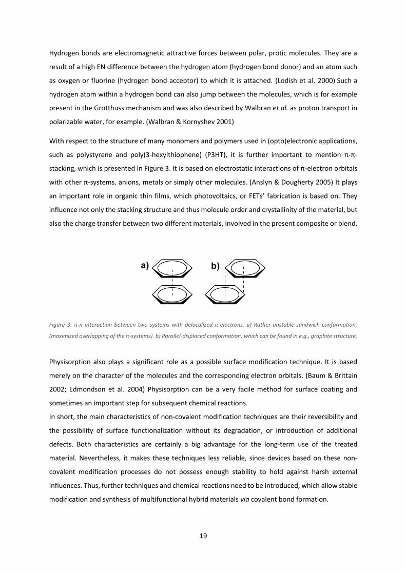
stacking, which is presented in Figure 3. It is based on electrostatic interactions of π-electron orbitals
with other π-systems, anions, metals or simply other molecules. (Anslyn & Dougherty 2005) It plays
an important role in organic thin films, which photovoltaics, or FETs’ fabrication is based on. They
influence not only the stacking structure and thus molecule order and crystallinity of the material, but
also the charge transfer between two different materials, involved in the present composite or blend.
Figure 3: π-π interaction between two systems with delocalized π-electrons. a) Rather unstable sandwich conformation,
(maximized overlapping of the π-systems). b) Parallel-displaced conformation, which can be found in e.g., graphite structure.
Physisorption also plays a significant role as a possible surface modification technique. It is based
merely on the character of the molecules and the corresponding electron orbitals. (Baum & Brittain
2002; Edmondson et al. 2004) Physisorption can be a very facile method for surface coating and
sometimes an important step for subsequent chemical reactions.
In short, the main characteristics of non-covalent modification techniques are their reversibility and
the possibility of surface functionalization without its degradation, or introduction of additional
defects. Both characteristics are certainly a big advantage for the long-term use of the treated
material. Nevertheless, it makes these techniques less reliable, since devices based on these non-
covalent modification processes do not possess enough stability to hold against harsh external
influences. Thus, further techniques and chemical reactions need to be introduced, which allow stable
modification and synthesis of multifunctional hybrid materials via covalent bond formation.
20
1.1.2. Covalent Surface Modification
The bond dissociation energy (BDE) between two carbon atoms is about 347 kJ/mol, which is only
surpassed by C-H (410 kJ/mol) and C-F bonds (490 kJ/mol). (Smith & March 2006) Therefore, any
molecular structure based on C-C bonds provides a suitable template for stable composites. (Blanksby
& Ellison 2003) Because of this, the functionalization of for example via chemical vapor deposition
(CVD) grown graphene as 2D carbon monolayer (Whitener 2014), or freestanding graphene
nanosheets (RamanathanT. et al. 2008), graphene nanotubes (R. Wang et al. 2010), carbon nanotubes
(CNTs) (Yan et al. 2007) and also aerographite (Mecklenburg et al. 2012) has been intensively studied
during the last decades. However, with the rise of further novel nanomaterials, additional bond
formations and synthesis techniques of various hybrid systems have emerged becoming more
significant. (Chandiramouli & Nagarajan 2016; Dasog et al. 2013)
The BDE of Si-Si bond is 222 kJ/mol (King 2006), which is lower than C-C bonds. The energy for Si-H
bonds (318 kJ/mol) (King 2006), is smaller than C-H bonds, promising an easier cleavage of the bond
and subsequent modification of the Si based material surface. This allows less harsh reaction
conditions at for example lower temperatures, which is desirable for industrial use. This enables
silicon, one of the most prominent elements in industry, to be successfully modified. (Walsh et al.
2005)
Bulk silicon has been modified over decades by several research groups. (Lu et al. 2009; Hu et al. 2001;
Islam et al. 2016) The main goal was the functionalization of the silicon surface for interface processes
and surface engineering. Buriak et al. have shown that Si(100) and Si(111) surfaces are important for
various electronic applications. (Buriak 2002) Additionally, both faces possess stability during
operation at atmospheric pressures and at high vacuum, while being exposed to different solvents. At
the same time, they have the already mentioned high reactivity at the surface, which is desirable for
the ease of chemical reactions. This makes them suitable for modification and functionalization
reactions with low energy requirements. (Buriak 2002)
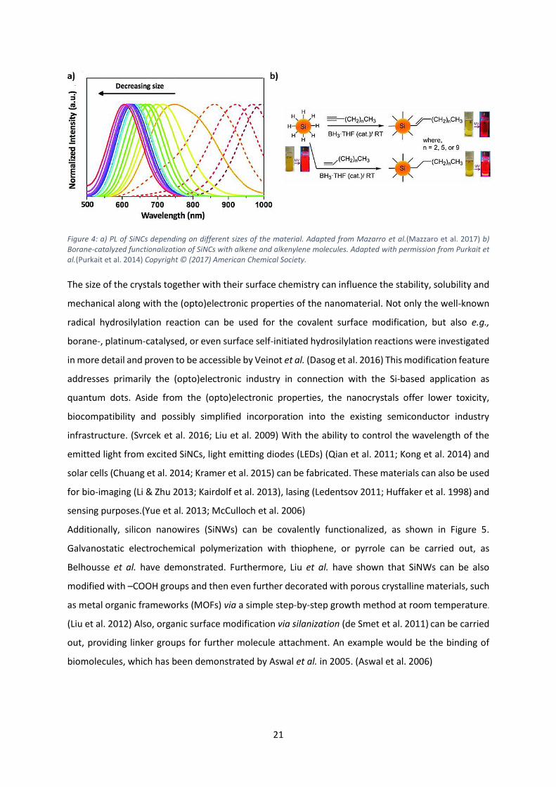
Silicon nanocrystals (SiNCs) surfaces are also highly reactive. Thus, going back to the nano-dimensions,
but keeping the silicon as our main element, SiNCs have been successfully functionalized with various
molecules and their properties controlled. Dasog et al. demonstrated a wide range of modification
methods for the nanocrystals’ surface (Dasog et al. 2016), which allow a precise engineering of their
luminescent properties (Figure 4).
21
Figure 4: a) PL of SiNCs depending on different sizes of the material. Adapted from Mazarro et al.(Mazzaro et al. 2017) b) Borane-catalyzed functionalization of SiNCs with alkene and alkenylene molecules. Adapted with permission from Purkait et al.(Purkait et al. 2014) Copyright © (2017) American Chemical Society.
The size of the crystals together with their surface chemistry can influence the stability, solubility and
mechanical along with the (opto)electronic properties of the nanomaterial. Not only the well-known
radical hydrosilylation reaction can be used for the covalent surface modification, but also e.g.,
borane-, platinum-catalysed, or even surface self-initiated hydrosilylation reactions were investigated
in more detail and proven to be accessible by Veinot et al. (Dasog et al. 2016) This modification feature
addresses primarily the (opto)electronic industry in connection with the Si-based application as
quantum dots. Aside from the (opto)electronic properties, the nanocrystals offer lower toxicity,
biocompatibility and possibly simplified incorporation into the existing semiconductor industry
infrastructure. (Svrcek et al. 2016; Liu et al. 2009) With the ability to control the wavelength of the
emitted light from excited SiNCs, light emitting diodes (LEDs) (Qian et al. 2011; Kong et al. 2014) and
solar cells (Chuang et al. 2014; Kramer et al. 2015) can be fabricated. These materials can also be used
for bio-imaging (Li & Zhu 2013; Kairdolf et al. 2013), lasing (Ledentsov 2011; Huffaker et al. 1998) and
sensing purposes.(Yue et al. 2013; McCulloch et al. 2006)
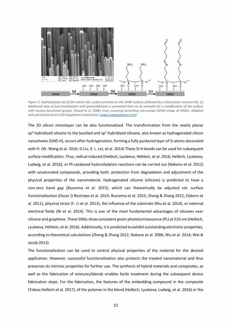
Additionally, silicon nanowires (SiNWs) can be covalently functionalized, as shown in Figure 5.
Galvanostatic electrochemical polymerization with thiophene, or pyrrole can be carried out, as
Belhousse et al. have demonstrated. Furthermore, Liu et al. have shown that SiNWs can be also
modified with –COOH groups and then even further decorated with porous crystalline materials, such
as metal organic frameworks (MOFs) via a simple step-by-step growth method at room temperature.
(Liu et al. 2012) Also, organic surface modification via silanization (de Smet et al. 2011) can be carried
out, providing linker groups for further molecule attachment. An example would be the binding of
biomolecules, which has been demonstrated by Aswal et al. in 2005. (Aswal et al. 2006)
22
Figure 5: Hydroxylation (a) of the native SiOx surface present on the SiNW surface, followed by a silanization reaction (b). (c) Additional step of functionalization with glutaraldehyde is presented here as an example for a modification of the surface with various functional groups. (Aswal et al. 2006) Inset: scanning tunnelling microscope (SEM) image of SiNWs. Adapted with permission from CVD Equipment Corporation (www.cvdequipment.com)
The 2D silicon monolayer can be also functionalized. The transformation from the nearly planar
sp2-hybridized silicene to the buckled and sp3-hybridized silicane, also known as hydrogenated silicon
nanosheets (SiNS-H), occurs after hydrogenation, forming a fully puckered layer of Si atoms decorated
with H. (W. Wang et al. 2016; G Liu, X. L. Lei, et al. 2014) These Si-H bonds can be used for subsequent
surface modification. Thus, radical-induced (Helbich, Lyuleeva, Höhlein, et al. 2016; Helbich, Lyuleeva,
Ludwig, et al. 2016), or Pt-catalysed hydrosilylation reactions can be carried out (Nakano et al. 2012)
with unsaturated compounds, providing both: protection from degradation and adjustment of the
physical properties of the nanomaterial. Hydrogenated silicene (silicane) is predicted to have a
non-zero band gap (Buscema et al. 2015), which can theoretically be adjusted via: surface
functionalization (Oscar D Restrepo et al. 2014; Buscema et al. 2015; Zheng & Zhang 2012; Osborn et
al. 2011), physical strain (F. Li et al. 2013), the influence of the substrate (Niu et al. 2014), or external
electrical fields (Ni et al. 2014). This is one of the most fundamental advantages of silicanes over
silicene and graphene. These SiNSs show consistent green photoluminescence (PL) at 510 nm (Helbich,
Lyuleeva, Höhlein, et al. 2016). Additionally, it is predicted to exhibit outstanding electronic properties,
according to theoretical calculations (Zheng & Zhang 2012; Nakano et al. 2006; Wu et al. 2014; Wei &
Jacob 2013)
The functionalization can be used to control physical properties of the material for the desired
application. However, successful functionalization also protects the treated nanomaterial and thus
preserves its intrinsic properties for further use. The synthesis of hybrid materials and composites, as
well as the fabrication of mixtures/blends enables facile treatment during the subsequent device
fabrication steps. For the fabrication, the features of the embedding compound in the composite
(Tobias Helbich et al. 2017), of the polymer in the blend (Helbich, Lyuleeva, Ludwig, et al. 2016) or the
23
molecule on the surface (Helbich, Lyuleeva, Höhlein, et al. 2016) can be used, which can be covalently,
or non-covalently bound. As a result, e.g., the melting temperature of the composite (due to the
polymer, such as SiNS-polymer@polymer), the solubility of the blend (e.g., SiNS-R/P3HT), or the
homogeneity of the hybrid materials in general and with it the interaction of the sheets within the
polymer can be achieved. This use of both materials properties is a valuable tool and a benefit for
subsequent improvement of the device performance.
Hydrophobic and hydrophilic SINSs can be dispersed and used for further treatment and fabrication
steps. Additionally, controlled dispersibility in various liquid environments ensures reproducibility
during already well-known and established fabrication techniques, such as spray- (Abdellah &
Abdelhalim 2013), spin- (Melzer et al. 2014), or dip-coating. (Harun et al. 2012) With these techniques,
ordered structures and thin films can be prepared using dissolved, or dispersed composites/blends.
(Xie et al. 2016) Inkjet printing is another powerful and easily accessible method, which enables access
to a variety of patterns. These patterning techniques are applicable for sensing areas of the device
and for electrodes printing. (Fiori et al. 2014; Torrisi et al. 2012)
Additionally, this fabrication technology can be applied to a number of various supporting substrates.
Various substrates can be chosen for the device preparation, since these methods allow not only the
treatment of rigid, but also uneven, flexible and deformable surfaces. This enables the fabrication of
“wearables”, such as on-skin electronics (Miyamoto et al. 2017; Yokota et al. 2016) and smart tattoos
(Kao et al. 2016) which have become the subject of intense investigation. The ability to print
conductive materials on skin, stretchable plastics, wires of cloths and even contact lenses requires
high accuracy. (Stoppa & Chiolerio 2014) The primary basis for this utilizes a well-dispersed
nanomaterial in a solvent, which can be easily and rapidly evaporated. However, it is important that
these nanomaterials are biocompatible. (Ray et al. 2009)
As a result, these advances in sample preparation have led to the fabrication of new transistors (Gao
et al. 2012; Oscar D. Restrepo, Mishra, et al. 2014), photodetectors (Koski & Cui 2013), photovoltaic
solar cells (Okamoto et al. 2011) and lithium-ion batteries. (Kumai, Shirai, et al. 2011; Kumai, Kadoura,
et al. 2011; Kumai & Nakano 2015)
24
1.2. THE RISE OF 2D SILICON NANOMATERIALS: SILICENE & SILICANE
1.2.1. Silicene – From Synthesis to Application
This work concentrates on silicon in its 2D form, which will be described and analyzed for
(opto)electronic device application. Freestanding silicon nanosheets (SiNSs) represent one of the 2D
form of silicon-based materials, while being only one atom layer thick. As already mentioned, 2D
silicon was first mentioned by Takeda and Shiraishi in 1994 (Takeda & Shiraishi 1994) and then got
forgotten for more than 10 years, until it was reinvestigated using theoretical studies by Guzmann-
Verri et al. (Guzmán-Verri & Lew Yan Voon 2007) As they were able to show with a tight-binding
Hamiltonian, silicene is expected to be a semi-metal. Once again, it is built of a sp2-hybridized nearly
planar monolayer of honeycomb structured silicon atoms, has a zero-band gap and additionally, the
presence of Dirac cones has been for the first time demonstrated in 2007. (Guzmán-Verri & Lew Yan
Voon 2007) Furthermore, it has an ambipolar Dirac charge transport, which was theoretically
predicted by Kim et al. in 2009. (Kim et al. 2009)
However, without an experimental evidence of this so-called “new cousin of graphene” (Le Lay et al.
2016), the fundamental studies around it reached an impasse. After the first synthesis of silicon
nanoribbons on a silver substrate Ag (110) using an ultrahigh vacuum deposition technique in 2009
(Kara et al. 2009), the successful synthesis of silicene on Ag (111) was shown. (Vogt et al. 2012; Lin et
al. 2012; Feng et al. 2012; Chiappe et al. 2012) Additionally, silicene could also be considered for
transparent and flexible electronics, as it is a monolayered material. Thus, the long-awaited first
experimental success was achieved by Tao et al., who proved the outstanding physical properties of
silicene, after building the first silicene based FET in 2015. (Tao et al. 2015)
Nevertheless, to realize stable reliable application, the drawbacks need to be overcome, such as the
already mentioned stability of the material. The Nobel laureate Roald Hoffmann has stated: “I don’t
often say something categorical, but I will say that a pristine free-standing single layer sheet of silicene
(or a Si nanotube) will not be made. Silicene exists and will be made only on a support of some sort,
metal or semiconductor”. (Hoffmann 2004) So far, his prediction has not been proven wrong.
25
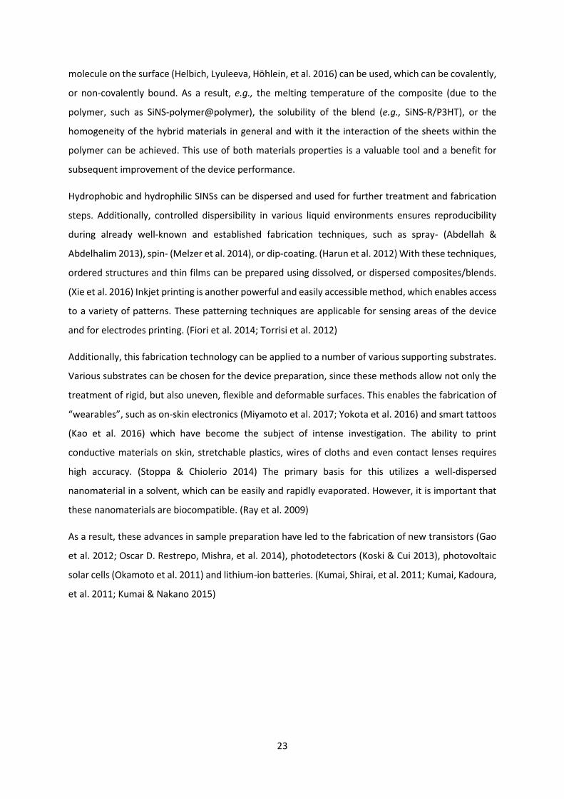
Figure 6: (a) Silicene plane image showing a honeycomb mesh of silicon atoms. Top-view (b) on a Si six-ring with lattice parameters and side-view (c) of a low-buckled silicon monolayer with a buckling height. Adapted from Peng et al. (Peng et al. 2013) with permission of The Royal Society of Chemistry.
The crystallographic thickness of silicene is 0.16 nm, as it was calculated from the atomic architecture.
The experimentally measured thickness by H. Nakano (Nakano 2014), using atomic force microscopy
(AFM) surface analysis technique, shows single layer thickness of about 0.4 nm. This difference to the
theoretically predicted thickness is explained with the oxygen encapsulation, which takes place
immediately after the material comes into contact with air.
Silicene was grown on rigid, mostly metallic substrates in UHV conditions. Hereby, only inert
substrates with a negligible chemical reactivity, such as Ag(111), can be used, which is probably the
most studied system, starting with reports in 2012. (Vogt et al. 2012; Grazianetti et al. 2016) The
influence of the substrate is important, as it turns out to be an effective method to manipulate and
thus shift the band gap of the as grown material. (Guo et al. 2015; Cahangirov et al. 2013; Guo et al.
2013) So far, aside from the already mentioned Ag support (Vogt et al. 2012; Lin et al. 2012), many
substrates have been investigated for the experimental growth of silicene, such as ZrB2 (Fleurence et
al. 2012), Ir (Meng et al. 2013) and MoS2 (Chiappe et al. 2014). In general, the influence of the
substrates is strong enough to destroy the Dirac nature of monolayered materials (Spencer 2016),
which needs to be prevented in the future and has been succesfully accomplished with the previously
mentioned fabrication of the silicene based FET. (Tao et al. 2015) In their study, the silicon monolayer
is covered by AlO2 thin film and delaminated from the surface it was grown on, to get rid of the
substrate’s destructive influence. While measurements could be carried out, the material was still not
stable enough for long-term operation of the device. This allows both, the advantages of the
semiconducting properties of the nanomaterial and the initiated charge transitions between the
valence and conductance bands with possible subsequent photon generations.
26
1.2.2. Silicane – Hydrogenated Silicon Monolayer as a Novel Representative of an sp3-Hybridized
Freestanding 2D Silicon
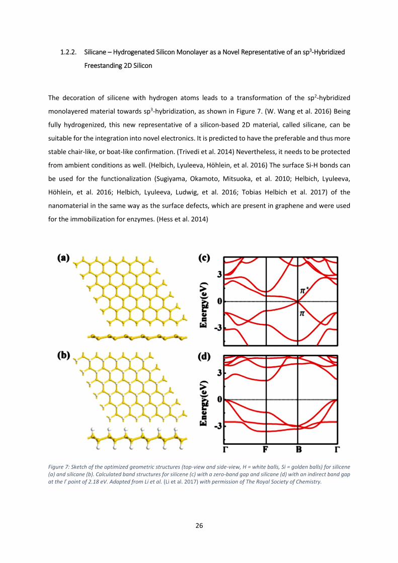
The decoration of silicene with hydrogen atoms leads to a transformation of the sp2-hybridized
monolayered material towards sp3-hybridization, as shown in Figure 7. (W. Wang et al. 2016) Being
fully hydrogenized, this new representative of a silicon-based 2D material, called silicane, can be
suitable for the integration into novel electronics. It is predicted to have the preferable and thus more
stable chair-like, or boat-like confirmation. (Trivedi et al. 2014) Nevertheless, it needs to be protected
from ambient conditions as well. (Helbich, Lyuleeva, Höhlein, et al. 2016) The surface Si-H bonds can
be used for the functionalization (Sugiyama, Okamoto, Mitsuoka, et al. 2010; Helbich, Lyuleeva,
Höhlein, et al. 2016; Helbich, Lyuleeva, Ludwig, et al. 2016; Tobias Helbich et al. 2017) of the
nanomaterial in the same way as the surface defects, which are present in graphene and were used
for the immobilization for enzymes. (Hess et al. 2014)
Figure 7: Sketch of the optimized geometric structures (top-view and side-view, H = white balls, Si = golden balls) for silicene (a) and silicane (b). Calculated band structures for siIicene (c) with a zero-band gap and silicane (d) with an indirect band gap at the Γ point of 2.18 eV. Adapted from Li et al. (Li et al. 2017) with permission of The Royal Society of Chemistry.
27
The structural and electronic properties of silicane were first examined by Voon et al. in 2010 using
the ab-initio density functional theory (DFT) computations. (Lew Yan Voon et al. 2010) It is predicted
to have a non-zero band gap (Buscema et al. 2015), which should be adjustable via surface
functionalization (Oscar D Restrepo et al. 2014; Buscema et al. 2015; Zheng & Zhang 2012; Osborn et
al. 2011; Syaputra et al. 2015), physical strain (F. Li et al. 2013), the influence of the substrate (Niu et
al. 2014; Zhang et al. 2014), and/or external electrical fields (Ni et al. 2014). As already stated, this is
one of the most fundamental advantages of silicanes over the planar graphene and silicene. (Mohan
et al. 2015) Furthermore, this nanomaterial shows green photoluminescence (PL) at 510 nm (Helbich,
Lyuleeva, Höhlein, et al. 2016) and should also exhibit promising electronic properties according to
theoretical calculations. (Zheng & Zhang 2012; Nakano et al. 2006; Wu et al. 2014; Wei & Jacob 2013)
Upon hydrogenation, the buckling constant of the monolayered silicon increases from 0.45 Å to
0.72 Å, where the theoretical predictions show that the chair-like configuration is more energetically
favored than the boat conformation. (Lew Yan Voon et al. 2010; Zhang et al. 2012) Upon
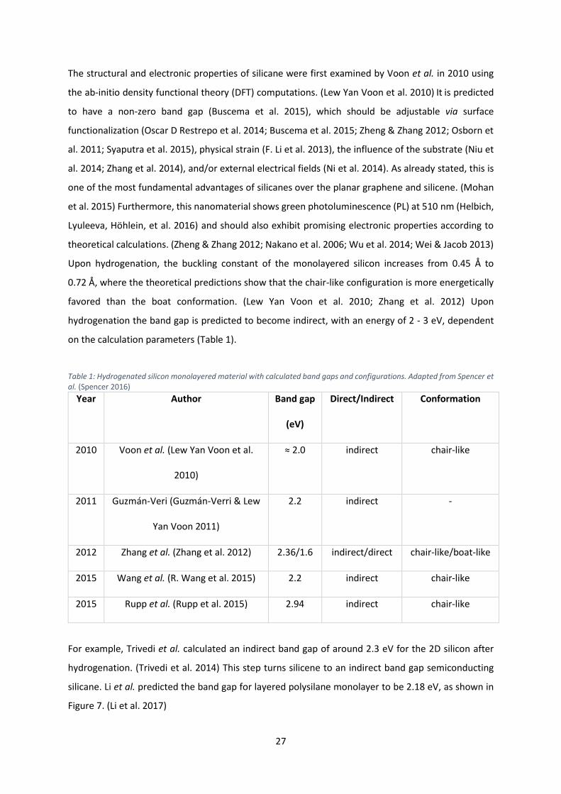
hydrogenation the band gap is predicted to become indirect, with an energy of 2 - 3 eV, dependent
on the calculation parameters (Table 1).
Table 1: Hydrogenated silicon monolayered material with calculated band gaps and configurations. Adapted from Spencer et al. (Spencer 2016)
Year Author Band gap
(eV)
Direct/Indirect Conformation
2010 Voon et al. (Lew Yan Voon et al.
2010)
≈ 2.0 indirect chair-like
2011 Guzmán-Veri (Guzmán-Verri & Lew
Yan Voon 2011)
2.2 indirect -
2012 Zhang et al. (Zhang et al. 2012) 2.36/1.6 indirect/direct chair-like/boat-like
2015 Wang et al. (R. Wang et al. 2015) 2.2 indirect chair-like
2015 Rupp et al. (Rupp et al. 2015) 2.94 indirect chair-like
For example, Trivedi et al. calculated an indirect band gap of around 2.3 eV for the 2D silicon after
hydrogenation. (Trivedi et al. 2014) This step turns silicene to an indirect band gap semiconducting
silicane. Li et al. predicted the band gap for layered polysilane monolayer to be 2.18 eV, as shown in
Figure 7. (Li et al. 2017)

28
At the same time, Houssa et al. have shown in their DFT based calculations the possibility for both:
boat- and chair-like configurations. Whereby, the chair configuration has an indirect band gap and the
boat configuration of the material possesses a direct band gap. (Houssa et al. 2011) Although the
indirect band gap is one of the main disadvantages of the material, it can still be used as an optically
active nanomaterial, if the band gap is controlled and shifted. Huang et al. have shown that with the
use of bilayer silicane, the band gap can be turned into a direct, or quasi-direct one with a promising
application in LED industry. (Huang et al. 2013)
29
2. METHODS AND FABRICATION TECHNIQUES
2.1. GENERAL INFORMATION
All reactants and reagents were purchased from Sigma-Aldrich, Alfa Aesar or Wacker and used without
further purification, if not stated otherwise. Toluene was dried prior to use with an MBraun solvent
purification system MB SPS-800 whereby argon 4.8 (99.998 %, Westfalen AG) was used as inert gas.
Acetone was dried over molecular sieve, degassed via 3 freeze-pump-thaw cycles and stored under
argon. For storage, the exfoliated SiNSs were placed in a glove box with argon 4.8 (99.998 %, Westfalen
AG). Air or water sensitive reactions were executed under standard Schlenk techniques. The SiNS-
substrate@polymer nanocomposites were compounded in a MicroCompounder (DACA Instruments).
For oxygen and argon plasma, Femto low-pressure plasma system (plasma cleaner) was used with
continuously adjustable radiofrequency generator (13.56 MHz; 0 - 300 W).
FTIR spectra were measured with a Bruker Vertex 70 FTIR using a Platinum ATR from Bruker. TGA
measurements were executed with a DSC 3+ Star system from Mettler Toledo with heating rates of
10 K/min and nitrogen flow rates of 10 mL/min. AFM measurements (contact mode, Asylum Research
MFP-3D AFM with an ARC controller) were performed after spin-coating (1500 rpm, 90 s) of the
polymer and the blends, or drop/dip-coating on Si/SiO2 substrates. SEM images were recorded with a
NVision 40 from Carl Zeiss (Germany) using an acceleration voltage of 1.0 kV beam energy.
2.2. SYNTHESIS AND FUNCTIONALIZATION OF SINSS
2.2.1. Synthesis of Silicane
In an argon atmosphere a mixture of calcium (Alfa Aesar, 99.5%) and silicon (Wacker, 99.99%) was
pressed to a pellet and melted in an arc furnace. The chemical exfoliation was performed as published
by Helbich et al. (Helbich, Lyuleeva, Höhlein, et al. 2016): HClconc. (100 mL) was cooled in a Schlenk flask
to -25 °C and CaSi2 (1.00 g) was added under Ar. The reaction was carried out for 7 d at -25 °C. The
resulting suspension was filtered under Schlenk conditions through a glass frit. The yellow residue was
washed with degassed acetone and dried under vacuum. The obtained (Si6H6)n were stored under Ar
atmosphere until further use.
2.2.2. Etching of Silicon Nanosheets (Helbich, Lyuleeva, Höhlein, et al. 2016)
In ethanol dispersed (Si6H6)n (0.090 g) were placed in an ultrasonic bath for 2 min. Water (2 mL) and
aqueous HFconc.(0.25 mL) were added and extracted with dichloromethane (3 × 5 mL) into PTFE
30
centrifuge tubes. Toluene (40 mL) was added to the dispersion, which was subsequently centrifuged
(9000 rpm, 4 min). The SiNSs on the bottom of the tube were re-dispersed in acetone (2 mL) and
centrifuged again. After washing with toluene (2 mL) and last centrifugation, the SiNSs were dispersed
in toluene (for ThAc) or the neat substrate (for PhAc, 1-dodecene, tBMA) for further reactions.
2.2.3. Functionalization of SiNSs in the Microwave-reactor System
Reaction of SiNSs with dodecene and phenylacetylene was achieved in Schlenk conditions via mixing
SiNSs with the substrate (2.5 mL) in a microwave (MW) tube. The used MW reactor was
a Discover-S from CEM and was controlled by the software Synergy 1.58. The degassed (three times
via freeze-pump-thaw) dispersion in a vessel was transferred into the MW reactor. After MW
irradiation (2 h, 180 °C, no further cooling) with a different MW powers of up to 300 W, the mixture
was transferred into a sealed PTFE centrifuge tube with Ar and centrifuged (9000 rpm, 4 min). The
functionalized SiNSs were washed (3 x degassed acetonitriledry (3 mL) and toluene (0.5 mL)) and
centrifuged (9000 rpm, 4 min) again. After the dispersion of the SiNS-substrate in Et2O, the product
was dried under reduced pressure. For the functionalization with phenylacetylene (PhAc), the solid
side product was dissolved in toluene and removed (vide infra). For the functionalization with
2-ethinyl-3-hexylthiophene (ThAc), the SiNSs were dispersed in toluene (2 mL) and the substrate
(0.5 mL). For the alkyne functionalization, the cleaning step was extended by three washing steps with
acetonitrile. SiNS-C12H25 (SiNS-Dodecene) was synthesized as yellow, SiNS-PhAc (SiNS-styrenyl) as
orange-yellow and SiNS-ThAc (SiNS-thiopheneacethylene) as brown-bronze nanomaterial.
2.2.4. Functionalization of SiNS for humidity sensors:
The dispersion of SiNS-H in degassed toluenedry (12 mL, corresponds to 88 mg (Si6H6)n) was mixed in a
Schlenk tube with the monomer tBMA (3.3 g, 3 wt% of exfoliated (Si6H6)n). The dispersion was degassed
(3x freeze-pump-thaw cycles) and AIBN (20 mg) added to the mixture. After stirring for 16 h at 70 °C,
the reaction mixture was diluted and centrifuged (9000 rpm, 4 min). The hybrid material was
re-dispersed (3x) in toluene (0.5 mL), centrifuged and isolated by freeze-drying from benzene. FTIR
spectroscopy measurements were taken after drop-deposition of the material on the target substrate.
2.2.5. Hydrolyzation reaction of tBMA functional groups for humidity sensor
After the functionalization with the tert-butyl group, the protecting group (tert-butyl) was removed
by acid induced hydrolyzation reaction. The functionalized SiNS-tBMA were dispersed in
dichloromethane (2 mL) and trifluoromethansulfonic acid (5 drops) were added. The reaction mixture
was stirred in the dark (20 min) and centrifuged after washing with toluene (5 mL). After removal of
the centrifugate, the SiNSs residue was dispersed in ethanol (5 mL). Then, toluene (20 mL) was added
and the suspension centrifuged again (9000 rpm, 4 min). The purified SiNSs were dispersed in ethanol
31
for further use. FTIR spectroscopy measurements were taken after drop-deposition of the material on
the target substrate.
2.2.6. AIBN-initiated radical-induced functionalization reaction of SiNS-substrate@polymer
A dispersion of SiNS-H (corresponding to 0.088 g exfoliated (Si6H6)n) in degassed toluenedry (or ethanol
for AA) (12 mL) were mixed with 3 wt% (with regard to compound before etching) of the exfoliated
(Si6H6)n substrate (3.30 g) in a Schlenk tube. AIBN (0.020 g) was added after degassing (3x freeze thaw
pump cycles) and the reaction mixture stirred at 70 °C for 16 h.
For the isolation of SiNS-substrate@polymer, the reaction mixture was centrifuged (2 min, 9000 rpm)
after precipitation in methanol (or toluene in the case of PAA). The solid was re-dispersed (2×),
precipitated, and isolated by freeze-drying from benzene (or water in the case of SiNS-PAA@PAA).
For the isolation of SiNS-substrate, the reaction mixture was diluted and centrifuged (2 min, 9000 rpm),
re-dispersed (3×) in the reaction solvent (0.5 mL), centrifuged, and freeze dried from benzene (or
water for SiNS-PAA). Table 2 summarizes the materials used in the reaction.
Table 2: Substrates, which were used for the radical induced reactions and the corresponding solvents.
substrate
M
(g·mol−1)
m
(g)
N
(mmol)
solvent for
reaction
solvent for
precipitation
solvent for freeze
drying
styrene 104.06
0.500
4.80
toluene methanol benzene
MMA 100.05 5.00
AA 72.02 6.94 ethanol toluene water
2.3. PHOTOLITHOGRAPHY AND METAL EVAPORATION FOR INTERDIGITAL (IDE) STRUCTURE
PATTERNING
The substrate ( Si++/SiO2 wafer, or Kapton with 75 µm thickness) was cleaned and pre-heated at 110 °C
for 2 min. The Photoresist (AZ5214E) was coated on the substrate surface via spin-coating deposition
technique (100 rpm, 2.8 s; 3000 rpm, 20 s; 1000 rpm, 20 s; 6000 rpm, 6 s). Pre-baking of the photoresist
was carried out at 110 °C for 60 s. The coated wafer/Kapton film with the photoresist was then
exposed through the mask with the desired integrated finger structure to an Hg-lamp for photoresist
32
exposure (1.7 s) of the uncovered parts. Reversal baking step of the covered surfaces was carried out
on a hotplate at 125 °C (2 min), followed by the flood exposure step with Hg-lamp (> 200 mJ/cm2, 1
min). The treated thin-film on the substrate was exposed to a developer solution (AZ400K : water, 1 :
4, 20-25 s) to remove the soluble parts of the photoresist. The resulting structure on substrate is
shown in Figure 8, first left image.
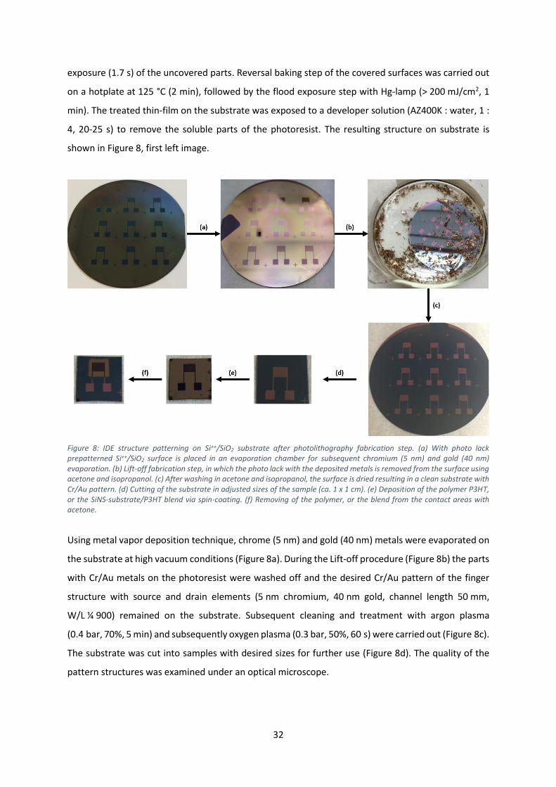
Figure 8: IDE structure patterning on Si++/SiO2 substrate after photolithography fabrication step. (a) With photo lack prepatterned Si++/SiO2 surface is placed in an evaporation chamber for subsequent chromium (5 nm) and gold (40 nm) evaporation. (b) Lift-off fabrication step, in which the photo lack with the deposited metals is removed from the surface using acetone and isopropanol. (c) After washing in acetone and isopropanol, the surface is dried resulting in a clean substrate with Cr/Au pattern. (d) Cutting of the substrate in adjusted sizes of the sample (ca. 1 x 1 cm). (e) Deposition of the polymer P3HT, or the SiNS-substrate/P3HT blend via spin-coating. (f) Removing of the polymer, or the blend from the contact areas with acetone.
Using metal vapor deposition technique, chrome (5 nm) and gold (40 nm) metals were evaporated on
the substrate at high vacuum conditions (Figure 8a). During the Lift-off procedure (Figure 8b) the parts
with Cr/Au metals on the photoresist were washed off and the desired Cr/Au pattern of the finger
structure with source and drain elements (5 nm chromium, 40 nm gold, channel length 50 mm,
W/L ¼ 900) remained on the substrate. Subsequent cleaning and treatment with argon plasma
(0.4 bar, 70%, 5 min) and subsequently oxygen plasma (0.3 bar, 50%, 60 s) were carried out (Figure 8c).
The substrate was cut into samples with desired sizes for further use (Figure 8d). The quality of the
pattern structures was examined under an optical microscope.

33
2.4. SGFET FABRICATION AND CHARACTERIZATION
2.4.1. SGFET fabrication:
P3HT was dissolved in a chosen solvent (1,2,-dichlorobenzene, Figure 9a) and stirred overnight at 60 °C
in a glovebox. The functionalized SiNSs (specific wt% of the P3HT-solution, Figure 9b) were dispersed
in the dissolved P3HT polymer.
Figure 9: (a) Image of the semiconducting polymer P3HT dissolved in 1,2-DCB. (b) SiNS-C12H25 powder after freeze-drying from benzene.
A drop of the prepared dispersions of P3HT and SiNS-substrate/P3HT blends was placed on the middle
of the pre-patterned and pre-cut Si++/SiO2 wafer or Kapton (polyimide, Figure 10 (a)) and spin coated
(1500 rpm, 90 s). Subsequently, it was annealed at 120 °C for 10 min (Figure 8e). The resulting polymer
and blend films (Figure 10 (b)) were approximately 50 to 70 nm thick.
Figure 10: (a) Flexible Kapton foil with the pre-patterned IDE structure and the drop-deposited functionalized SiNSs. (b) With SiNS-C12H25/P3HT coated SI++/SiO2 surface, the IDE structure with the thin film on top of it is visible with bar eyes.
(a) (b)
2 mm
34
2.4.2. Electrical Characterization
Electrical characterization of the fabricated devices was carried out using a Keithley source meter
(System 2636A).
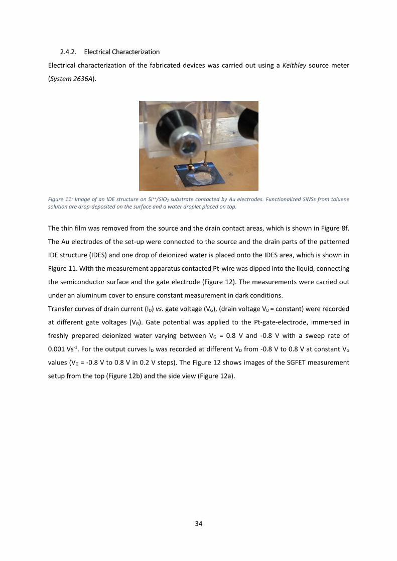
Figure 11: Image of an IDE structure on Si++/SiO2 substrate contacted by Au electrodes. Functionalized SiNSs from toluene solution are drop-deposited on the surface and a water droplet placed on top.
The thin film was removed from the source and the drain contact areas, which is shown in Figure 8f.
The Au electrodes of the set-up were connected to the source and the drain parts of the patterned
IDE structure (IDES) and one drop of deionized water is placed onto the IDES area, which is shown in
Figure 11. With the measurement apparatus contacted Pt-wire was dipped into the liquid, connecting
the semiconductor surface and the gate electrode (Figure 12). The measurements were carried out
under an aluminum cover to ensure constant measurement in dark conditions.
Transfer curves of drain current (ID) vs. gate voltage (VG), (drain voltage VD = constant) were recorded
at different gate voltages (VG). Gate potential was applied to the Pt-gate-electrode, immersed in
freshly prepared deionized water varying between VG = 0.8 V and -0.8 V with a sweep rate of
0.001 Vs-1. For the output curves ID was recorded at different VD from -0.8 V to 0.8 V at constant VG
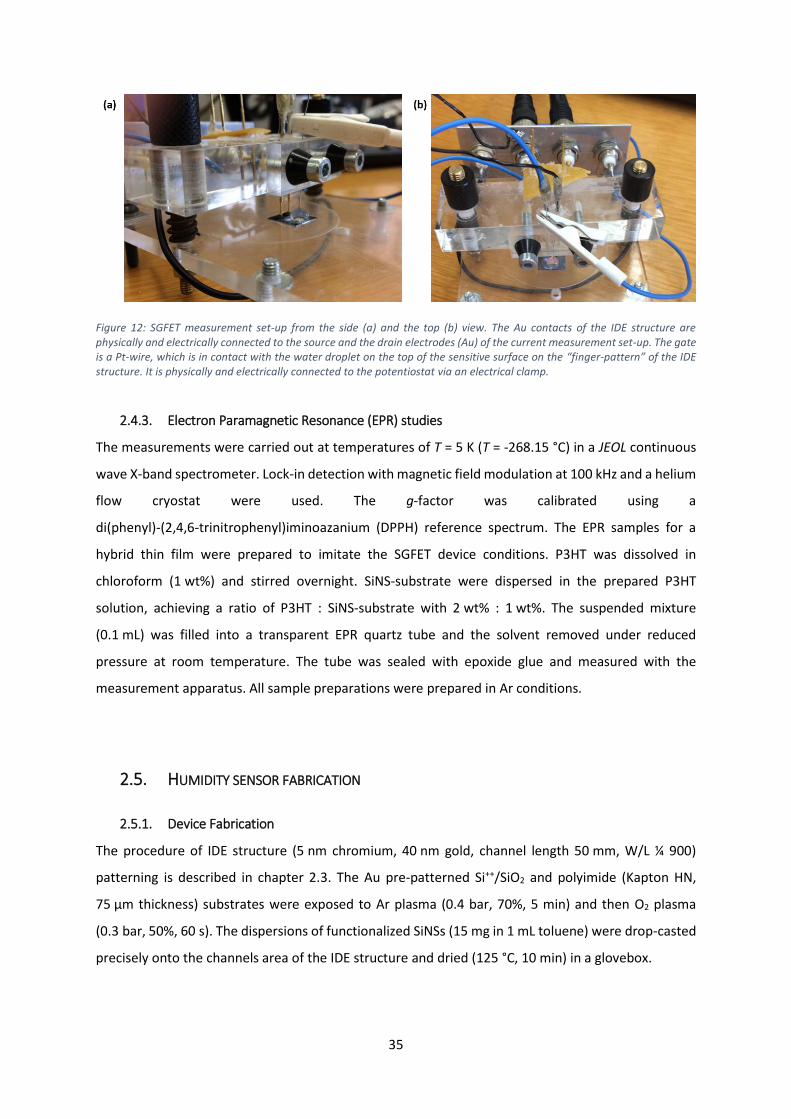
values (VG = -0.8 V to 0.8 V in 0.2 V steps). The Figure 12 shows images of the SGFET measurement
setup from the top (Figure 12b) and the side view (Figure 12a).
35
Figure 12: SGFET measurement set-up from the side (a) and the top (b) view. The Au contacts of the IDE structure are physically and electrically connected to the source and the drain electrodes (Au) of the current measurement set-up. The gate is a Pt-wire, which is in contact with the water droplet on the top of the sensitive surface on the “finger-pattern” of the IDE structure. It is physically and electrically connected to the potentiostat via an electrical clamp.
2.4.3. Electron Paramagnetic Resonance (EPR) studies
The measurements were carried out at temperatures of T = 5 K (T = -268.15 °C) in a JEOL continuous
wave X-band spectrometer. Lock-in detection with magnetic field modulation at 100 kHz and a helium
flow cryostat were used. The g-factor was calibrated using a
di(phenyl)-(2,4,6-trinitrophenyl)iminoazanium (DPPH) reference spectrum. The EPR samples for a
hybrid thin film were prepared to imitate the SGFET device conditions. P3HT was dissolved in
chloroform (1 wt%) and stirred overnight. SiNS-substrate were dispersed in the prepared P3HT
solution, achieving a ratio of P3HT : SiNS-substrate with 2 wt% : 1 wt%. The suspended mixture
(0.1 mL) was filled into a transparent EPR quartz tube and the solvent removed under reduced
pressure at room temperature. The tube was sealed with epoxide glue and measured with the
measurement apparatus. All sample preparations were prepared in Ar conditions.
2.5. HUMIDITY SENSOR FABRICATION
2.5.1. Device Fabrication
The procedure of IDE structure (5 nm chromium, 40 nm gold, channel length 50 mm, W/L ¼ 900)
patterning is described in chapter 2.3. The Au pre-patterned Si++/SiO2 and polyimide (Kapton HN,
75 µm thickness) substrates were exposed to Ar plasma (0.4 bar, 70%, 5 min) and then O2 plasma
(0.3 bar, 50%, 60 s). The dispersions of functionalized SiNSs (15 mg in 1 mL toluene) were drop-casted
precisely onto the channels area of the IDE structure and dried (125 °C, 10 min) in a glovebox.
36
2.5.2. Device Characterization
A SMA (SubMiniature version A) male connector was connected with Ag-paint to the electrodes ends
points. The automated (LabVIEW 2016) electrical measurements were carried out with control over
an impedance analyzer (Keysight E4990A) with an impedance probe kit (4294A1) for the sensor
readout. The excitation voltage applied in all measurements was direct-current voltage (VDC = 0) and
alternating current voltage (VAC = 500 mV) in the frequency range from 1 kHz to 10 MHz. A prior
calibration was carried out to compensate the parasitic elements. The sensor was placed in a climatic
chamber (VLC4006) with temperature and humidity control. The monitoring was performed over the
climatic chamber sensor system. For the RH sensing, the moisture content was ramped up in 10%
steps and held for 1 h to ensure a stable value in the whole chamber volume. Similar approach
accounts for the temperature sensing with 5 °C steps for 1 h.
2.6. PHOTONIC SENSOR FABRICATION
2.6.1. SiNS-substrate@polymer Sensor Analysis and Fabrication
For the photonic sensor fabrication, the dispersion of SiNS-tBMA (30 mg) in toluenedry (2 mL) was drop-
deposited onto pre-patterned Au/Cr contacts (40/5 nm) on Si++/SiO2 substrate in a glovebox. Prior to
that, the surface was cleaned with Ar plasma (0.3 mbar, 70% power, 1 min). The deposited material
was dried at 115 °C for 10 min.
The SiNS-substrate@polymer nanocomposites were compounded in a MicroCompounder (DACA
Instruments) at 100 rpm and 220 °C under N2 atmosphere. The composite was cut into small pieces,
placed and melted on top of the area of the surface with already deposited SiNS-tBMA material, while
heating at 125 °C. The SiNS-X@Polymer was pressed onto the surface. The device was allowed to cool
very slowly to room temperature immediately after deposition.
For AFM Analysis of the SiNS-tBMA hybrid material, spray-coating was performed with an air atomizing
nozzle from a commercially available air brush (Gabbert Triplex). The dispersed material was sprayed
onto the substrate, which was heated on a hotplate during the deposition. The deposited material
was then analyzed with AFM tapping mode technique.
2.6.2. Electrical Device Characterization
ID (A) vs. time t (ms) measurements were recorded at constant drain (transfer characteristics) and gate
(output characteristics) voltages (VG = 1 V, 1.2 V, …, 2 V) using a source meter (Keithley model 2636A).
37
Output curves (ISD vs. VD) were taken by sweeping VD = −5 V to 5 V. The device was illuminated with a
commercially available energy-saving lamp (9 W, 2500 K, 50 - 60 Hz, 60% light in 100 s).
2.7. MATERIAL PREPARATION FOR THE TIPL AND TRPL MEASUREMENTS
2.7.1. Measurements in solution
The material in solid state (SiNS-substrate powder, or SiNS-substrate@polymer composite) is
dispersed in toluenedry and transferred in a sealed quartz cuvette. The dispersion is reset via shaking
of the cuvette before each new measurement, except PL vs. time studies.
2.7.2. Measurements in solid state
The material (ca. 500 µm thickness) is drop-casted from toluene dispersion on a non-fluorescent glass
plate (1 mm thickness). The measurements of the composites are carried out after melting (125 °C)
the SiNS-substrate@polymer on a non-fluorescent glass substrate.
2.8. TIME-INTEGRATED PL (TIPL) AND TIME-RESOLVED PL (TRPL) MEASUREMENTS The measurements were carried out within the ATUMS collaboration at the University of Alberta in
Edmonton (Canada) together with the group of Prof. Frank Hegmann. SiNSs-substrate in the
corresponding solvent was transferred into a cuvette and measured at room temperature.
For the samples in solid state, the UV-fused quartz glass with drop-deposited material was placed on
the copper finger with a whole in the middle of an optical microscopy cryostat (Cryo Industries) and
measured in ambient conditions. Then it was measured in vacuum (p = 2.2 × 10⁻⁷ mbar). Then, the
cryostat with the sample was cooled by free-flowing liquid nitrogen (LN2) with the aid of a temperature
controller (Lakeshore 335) and the data recorded in 10 °C steps. Low temperature compatible Apeizon
grease was used to adhere the edges of the quartz glass onto the copper sample holder. An 800 nm
Ti:Sapphire ultrafast laser (Coherent RegA 900) with 65 fs pulse width and 250 kHz repetition rate was
used to optically excite the samples at 400 nm via second harmonic signal generation from a BBO
crystal. All measurements were carried out at an average of 435 ± 5 µW excitation power. The PL was
collected by an objective (20x Mitutoyi M Plan Apo) and filtered by a 435 nm long pass filter (Edmund
Optics). The TIPL was measured for 0.5 seconds by a CCD (Princeton Instruments Acton Spectrometer)
with a resolution of ± 1.28 nm at 200 µm slit. For the nanosecond timescale TRPL, a time-correlated
single photon counting (TCSPC) technique was employed, which consists of a single-photon avalanche
38
photodiode connected to a TCSPC module (PicoHarp 300, Picoquant). The instrument response,
determined from the convolution fit to Gaussian function, provides a time resolution of 35 ± 1 ps,
where g(t)=G x exp (‐4ln(2)·(t‐t0)2
w2 ) and f(t) are the Gaussian and inverse power law functions,
respectively. The convolution (f*g)(t)= ∫ f(t‐τ) g(τ) dτ provides the width of the Gaussian, w,
corresponding to the width of the instrument’s impulse response.
During the TRPL measurements, low probability of registering more than one photon per cycle must
be maintained. For that, number of counts that is less than 10% of the laser repetition rate (25 kHz) is
kept constant in order to maintain a relative statistical error of less than σ = 10%. (Prasankumar &
Taylor 2011) Counts per min of less than 10,000 were maintained. The samples were cooled for at
least 10 min before each TRPL measurement. The TRPL data were fitted from 0.1 ns to prevent
contribution of the instrument response, until the baseline which is the average of the dark counts.
For measurements of the µs lifetime component, a Si-avalanche photodetector (Thorlabs APD130A,
20 ns time resolution) and a fast oscilloscope (Tektronix DPO 2024B, 200 MHz) were used instead.
2.9. TRANSMITTANCE MEASUREMENTS The External Quantum Efficiency (EQE) is measured, using a xenon arc lamp (300 W, 77 Hz) chopped
at 77 Hz through an Oriel Cornerstone 260 ¼ m monochromator (Newport Corporation, Irvine, CA,
USA) and an Oriel Merlin digital lock-in amplifier (Newport Corporation, Irvine, CA, USA).
39
3. RESULTS AND DISCUSSION
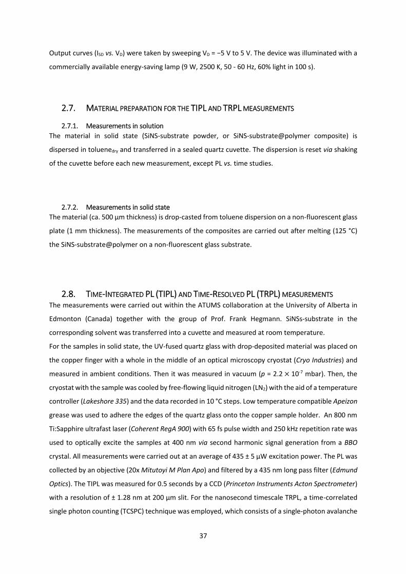
3.1. SYNTHESIS, FUNCTIONALIZATION AND CHARACTERIZATION
The synthesis of freestanding silicane (SiNSs) is mainly carried out via chemical exfoliation starting
from the Zintl-phase calcium disilicide (CaSi2). (Nakano et al. 2006) The product after the soft chemical
deintercalation of calcium atoms can be the layered polysilane (Si6H6) and siloxene (Si6H3(OH)3) (Dahn
et al. 1993), depending on the reaction conditions. Both materials have a backbone of puckered silicon
2D layers similar to the (111) planes of the bulk silicon. (P. Wang et al. 2016) The slightly buckled Si
layers are separated by Ca2+ planar monolayers (Figure 13a).
Figure 13: (a) Synthesis of 2D layered polysilane (silicane) from CaSi2 with HClconc. at -25°C. (b) X-ray powder diffraction pattern of freshly synthesized SiNSs showing (001), (100) and (110) peaks of Si. Adapted from Helbich et al.(Helbich, Lyuleeva, Ludwig, et al. 2016) with permission of John Wiley and Sons.
During the deintercalation of calcium cations from the layered structure with concentrated
hydrochloric acid at -25 to -35°C, the crystalline structure of CaSi2 collapses, which results in the
40
liberation of freestanding silicon nanosheets (SiNSs). As already mentioned, also full hydrogenation
(Sugiyama, Okamoto & Nakano 2010; Helbich, Lyuleeva, Höhlein, et al. 2016), or hydrogenation
rendered with hydroxylation (Dahn et al. 1993; Yamanaka et al. 1996) of the material takes place
during the process, depending on the temperature of this reaction step. The sketch of the reaction
and the power diffraction pattern of the freshly synthesized silicane (SiNS-H) is shown in Figure 13.
CaCl2 is formed as a by-product during the reaction and can be easily washed away during the work-up
procedure.
Right after the deintercalation of the Ca2+ ions, the SiNSs do not show any visible PL. However, after
the etching step of the nanomaterial with concentrated hydrofluoric acid, a green PL peaking at
510 nm could be observed. Figure 14 shows the emission (%) vs. wavelength (nm) spectrum of SiNS-H
sheets dispersed in toluene.
Figure 14: PL spectrum showing emission (%) vs. wavelength (nm) of the as prepared UV (λ = 365 nm) irradiated SiNS-H dispersed in toluene.
Using the sp3-character of silicane, the surface of the layered material can be modified, aiming for
multifunctional hybrid materials and composites. The radical hydrosilylation reaction is the
modification method of choice in this work. It can be initiated not only through temperature assisted
activation, but also with radical starters such as azobis(isobutyronitril) (AIBN) (Helbich, Lyuleeva,
Ludwig, et al. 2016), diazonium salts (e.g., 1,2-DDB) (Helbich, Lyuleeva, Höhlein, et al. 2016), lewis-acid
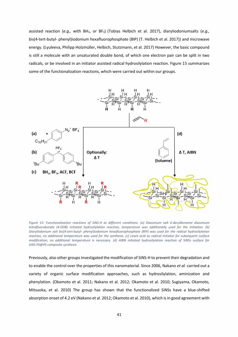
41
assisted reaction (e.g., with BH3, or BF3) (Tobias Helbich et al. 2017), diaryliodoniumsalts (e.g.,
bis(4-tert-butyl- phenyl)iodonium hexafluorophosphate (BIP) (T. Helbich et al. 2017)) and microwave
energy. (Lyuleeva, Philipp Holzmüller, Helbich, Stutzmann, et al. 2017) However, the basic compound
is still a molecule with an unsaturated double bond, of which one electron pair can be split in two
radicals, or be involved in an initiator assisted radical hydrosilylation reaction. Figure 15 summarizes
some of the functionalization reactions, which were carried out within our groups.
Figure 15: Functionalization reactions of SiNS-H at different conditions. (a) Diazonium salt 4-decylbenzene diazonium tetrafluoroborate (4-DDB) initiated hydrosilylation reaction; temperature was additionally used for the initiation. (b) Diaryliodonium salt bis(4-tert-butyl- phenyl)iodonium hexafluorophosphate (BIP) was used for the radical hydrosilylation reaction, no additional temperature was used for the synthesis. (c) Lewis acid as radical initiator for subsequent surface modification, no additional temperature is necessary. (d) AIBN initiated hydrosilylation reaction of SiNSs surface for SiNS-PS@PS composite synthesis.
Previously, also other groups investigated the modification of SiNS-H to prevent their degradation and
to enable the control over the properties of this nanomaterial. Since 2006, Nakano et al. carried out a
variety of organic surface modification approaches, such as hydrosilylation, aminization and
phenylation. (Okamoto et al. 2011; Nakano et al. 2012; Okamoto et al. 2010; Sugiyama, Okamoto,
Mitsuoka, et al. 2010) The group has shown that the functionalized SiNSs have a blue-shifted
absorption onset of 4.2 eV (Nakano et al. 2012; Okamoto et al. 2010), which is in good agreement with

42
our results presented in Figure 16. The non-functionalized SiNS-H show absorption (lowest
transmittance values) starting from 305 nm (4.01 eV) and the composite SINS-PS@PS even at lower
wavelengths, starting from 297 nm (4.17 eV).
Figure 16: (a) Transmission (%) vs. wavelength (nm) spectrum of etched SINS-H and SiNS-PS@PS composite. An absorption onset can be observed starting from 4.01 and 4.17 eV for SiNS-H and SiNS-PS@PS respectively. (b) AFM image of spin-deposited SiNS-C12H25 hybrid material from 1,2-dichlorobenzene (1,2-DCB) and the corresponding height profile z (nm) along the blue line in the AFM image.
Nonetheless, the type of the transition cannot be specified only from the plots, when comparing the
center wavelength energy Ecw from the PL spectra and with the plots estimated optical band edge Eg.
The onset of the absorption is within the PL spectra with no dramatic Stokes shift, which can be
observed with the Tauc’s plots with (αhν)2 for direct and (αhν)0.5 for indirect transition, calculated from
the PL spectra. The differences between the PL peak energies and estimated band gaps are around
0.03 eV, in the order of thermal energy at room temperature, which can also derived from the broad
PL peaks (ΔEPL = 0.330 – 0.375 eV, unlike PL from bulk crystalline semiconductor of around 0.047 eV
(1.8 kBT) at room temperature). (Lyuleeva, Mary A B Narreto, Helbich, Veinot, et al. 2017)
With these results, it is possible to consider fully hydrogenated and especially, due to the greater
stability, functionalized SiNSs for the use of this nanomaterial in optoelectronic applications. (Wei &
Jacob 2013; Hussain et al. 2014; G Liu, X. Lei, et al. 2014) Based on these considerations, our group
succeeded in the fabrication of a first prototyped photonic sensor, which can be used in ambient
conditions. The fabrication technique and the analysis will be discussed in Chapter 4.2.
43
3.2. PL AND TRPL STUDIES OF HYDROGENATED AND FUNCTIONALIZED SINSS.
As already mentioned, freshly synthesized and etched SiNSs exhibit green PL. The PL can be described
as relaxation of the electrons after their excitation with high energy light, during which photons are
emitted. The green PL of the functionalized SiNS is one of their remarkable properties, which origin is
still not completely understood. Most of the nanomaterials obey the phenomenon of quantum
confinement. (Delley & Steigmeier 1993; Delerue et al. 1993; Öğüt et al. 1997) It was also observed in
low-dimensional silicon, such as porous silicon (Canham 1990), silicon nanoparticles (Kabashin &
Meunier 2003), silicon nanocrystals (Takagi et al. 1990) and Si/SiO2 superlattices. (Vinciguerra et al.
2000) Nevertheless, not only quantum confinement, but also other effects such as interface states
(Wang et al. 2005; Luppi & Ossicini 2005), luminescent defects states (Kanemitsu 2002) and oxygen
vacancy states (Degoli & Ossicini 2000) at the Si/SiO2 interface were found to be the reason for the
emitted PL in e.g., SiNCs. However, the quantum confinement is still found by Derr et al. to be the
main reason for the PL in SiNCs. (Derr et al. 2009)
In this work, the PL of the differently functionalized SiNSs is analyzed and discussed. The chemical
treatment of the surface could influence its physical features, as it was shown in other various silicon-
based nanomaterials. (Spencer et al. 2013; Brennan, Morishita & Michelle J S Spencer 2016; Dasog et
al. 2014) With functional groups, it might be possible to push or pull the electrons towards and from
the surface respectively and thus shift the HOMO and LUMO edges of the gap. Also siloxane, being
functionalized not only with hydrogen atoms, but also hydroxy groups, was reported by Hengge et al.
in 1964 (Hengge & Grupe 1964) to have differences in the fluorescence dependent on the
functionalization. Nevertheless, SiNSs have a very broad (relatively high ΔEPL) green PL at around
510 nm, which does not shift in a controlled way: neither with different lateral sizes of the
nanomaterial, nor with various functional molecules covalently attached to the surface, which was
previously predicted by theoretical calculations. (Gao et al. 2012; Ding & Wang 2012) Freestanding 2D
SiNSs are consistently emitting green PL at 510 – 517 nm (around 2.40 - 2.45 eV, Figure 21b). This is
close to the value of e.g., the HF-treated layered polysilanes, reported by Nishimura et al., with the
PLmax at around 2.3 eV (540 nm). (Nishimura et al. 1996) Also the density functional theory (DFT)
calculations by Gang et al. confirm a band gap energy of about 2.4 eV. Thereby, the group studied the
influence of strain and electric field on the properties of the material. (Gang et al. 2013)
The broad PL spectral linewidth may be caused by the inhomogeneity of the surface, either coming
from the material itself, or from influences of the functional groups on the surface. Another reason
could be the broad variety of the lateral sizes of the sheets together with packed agglomerates in
dispersion. The lateral size can render from hundreds of nanometers up to several micrometers. Since

44
all particles can be excited and thus contribute to the emitted light, it may also cause broadening of
the PL. For example, Kim et al. studied 2D silicon-based material, which was grown on a substrate with
the CVD technique. The group has shown a clear PLmax dependence on the lateral size and thickness
of their nano-sized material. Although the nature of the by Kim and his co-workers presented sheets
is different, compared to the one of our layered material, it can provide a hint for understanding about
the dependence of the broadening of the PL linewidth on the size variety. (H. J. Kim et al. 2011)
Nevertheless, due to the difference in structure, it is very likely to have also a different behavior with
varying sizes, which will be confirmed in the following.
The stacking structure of the sheets and with it arising influences of the layers on each other should
also be considered as an impact on the PL. As discussed in our previous results (Helbich, Lyuleeva,
Höhlein, et al. 2016), SiNSs tend to easily agglomerate. These stacking structures form multi-layer
SiNSs systems, in which the single silicon monolayers may influence each other in terms of their
symmetry, lateral straightening and order. For example, Spencer et al. have demonstrated that the
stacked phenylated silicene can render its band gap with the distances between the sheets, going from
the infinite, over minimum to the compressed-like distances. (Spencer et al. 2013) Furthermore,
diluted dispersions of the functionalized sheets lead to a small blue shift of the PLmax (Lyuleeva, Tobias
Helbich, Rieger & Lugli 2017), which confirms its additional dependence on the agglomerates
formation. Agglomerates tend to form in more concentrated dispersions.
Being a potential additional reason for PL broadening, we could show that the tailing in the band gap
obeys the Urbach rule. As it will be described in more detail later in this chapter, it even turned out to
be the most important effect, observed with the PL broadening. Comparable to our results, also
siloxene show the Urbach-edge slope as the distribution of the size of the band gap, which was
described by Rosenbauer et al. in 1993. (Rosenbauer et al. 1993) But before we come to the
understanding of the origin of the PL, its behavior with time and during the irradiation will be analyzed.
To check the length of the emission time, PL intensity vs. time studies applying SiNS-C12H25
(SiNS-Dodecene) were carried out. The readily functionalized material (SiNS-C12H25 dispersed in
toluene) was chosen, due to the enhanced stability in air. Figure 17 shows PL intensity vs. wavelength
spectrum of the SiNS-C12H25 (dispersed in toluene). Fast decrease in the intensity is already observed
after 2 min of irradiation with the laser beam.
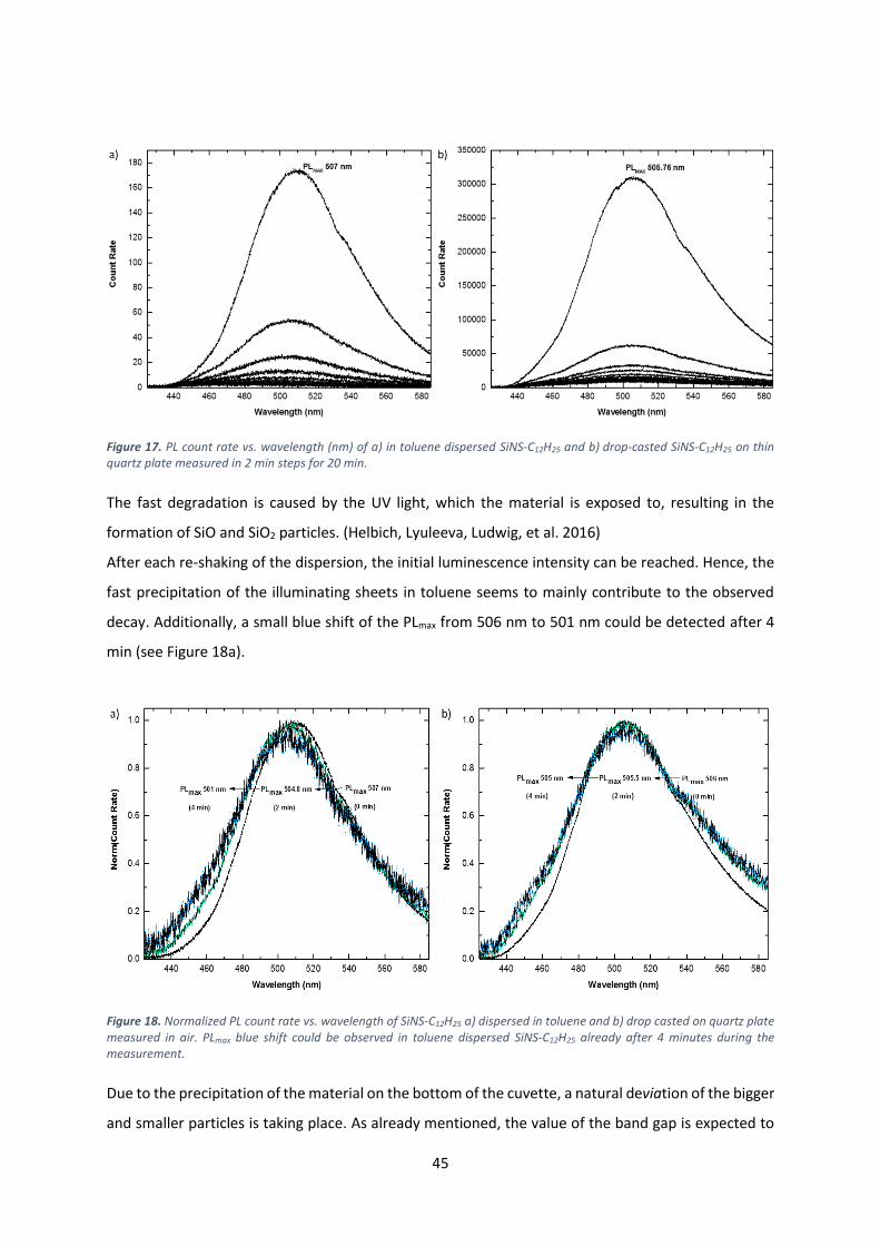
45
Figure 17. PL count rate vs. wavelength (nm) of a) in toluene dispersed SiNS-C12H25 and b) drop-casted SiNS-C12H25 on thin quartz plate measured in 2 min steps for 20 min.
The fast degradation is caused by the UV light, which the material is exposed to, resulting in the
formation of SiO and SiO2 particles. (Helbich, Lyuleeva, Ludwig, et al. 2016)
After each re-shaking of the dispersion, the initial luminescence intensity can be reached. Hence, the
fast precipitation of the illuminating sheets in toluene seems to mainly contribute to the observed
decay. Additionally, a small blue shift of the PLmax from 506 nm to 501 nm could be detected after 4
min (see Figure 18a).
Figure 18. Normalized PL count rate vs. wavelength of SiNS-C12H25 a) dispersed in toluene and b) drop casted on quartz plate measured in air. PLmax blue shift could be observed in toluene dispersed SiNS-C12H25 already after 4 minutes during the measurement.
Due to the precipitation of the material on the bottom of the cuvette, a natural deviation of the bigger
and smaller particles is taking place. As already mentioned, the value of the band gap is expected to
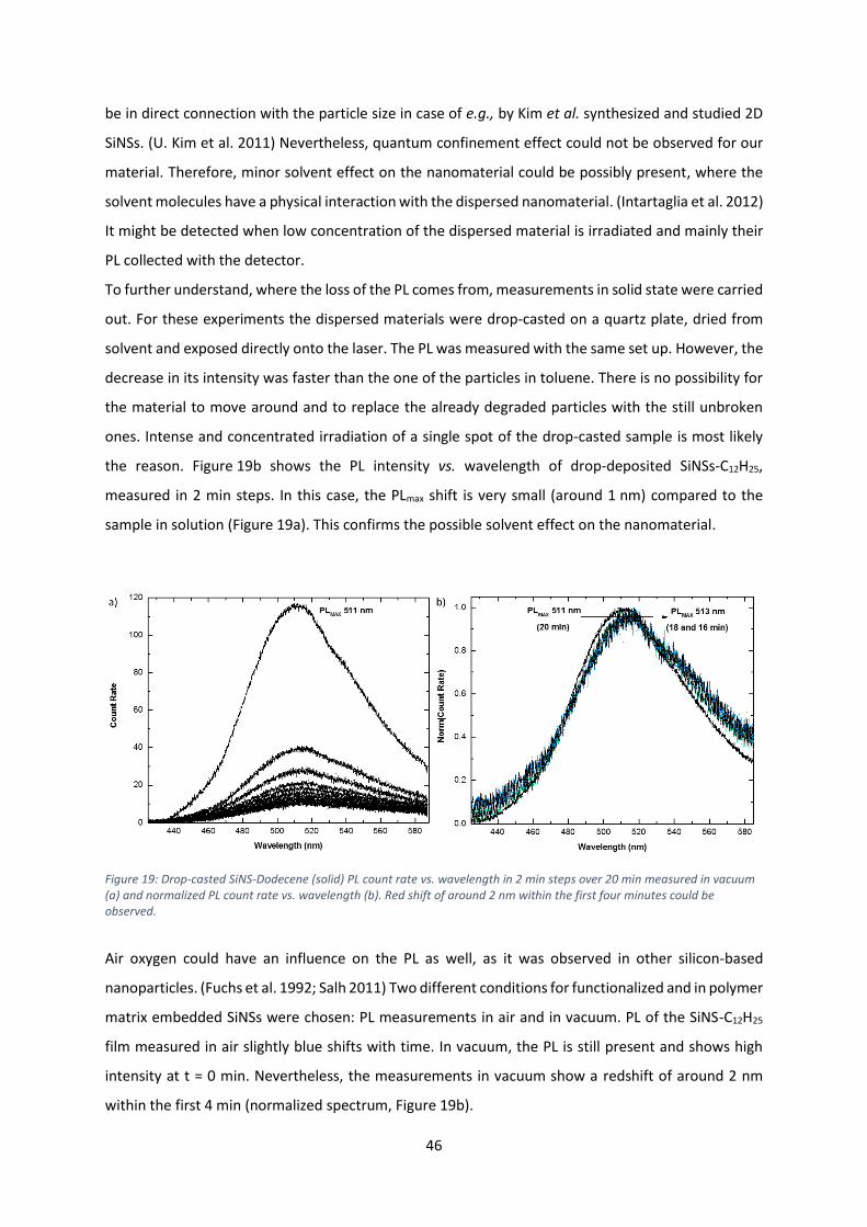
46
be in direct connection with the particle size in case of e.g., by Kim et al. synthesized and studied 2D
SiNSs. (U. Kim et al. 2011) Nevertheless, quantum confinement effect could not be observed for our
material. Therefore, minor solvent effect on the nanomaterial could be possibly present, where the
solvent molecules have a physical interaction with the dispersed nanomaterial. (Intartaglia et al. 2012)
It might be detected when low concentration of the dispersed material is irradiated and mainly their
PL collected with the detector.
To further understand, where the loss of the PL comes from, measurements in solid state were carried
out. For these experiments the dispersed materials were drop-casted on a quartz plate, dried from
solvent and exposed directly onto the laser. The PL was measured with the same set up. However, the
decrease in its intensity was faster than the one of the particles in toluene. There is no possibility for
the material to move around and to replace the already degraded particles with the still unbroken
ones. Intense and concentrated irradiation of a single spot of the drop-casted sample is most likely
the reason. Figure 19b shows the PL intensity vs. wavelength of drop-deposited SiNSs-C12H25,
measured in 2 min steps. In this case, the PLmax shift is very small (around 1 nm) compared to the
sample in solution (Figure 19a). This confirms the possible solvent effect on the nanomaterial.
Figure 19: Drop-casted SiNS-Dodecene (solid) PL count rate vs. wavelength in 2 min steps over 20 min measured in vacuum (a) and normalized PL count rate vs. wavelength (b). Red shift of around 2 nm within the first four minutes could be observed.
Air oxygen could have an influence on the PL as well, as it was observed in other silicon-based
nanoparticles. (Fuchs et al. 1992; Salh 2011) Two different conditions for functionalized and in polymer
matrix embedded SiNSs were chosen: PL measurements in air and in vacuum. PL of the SiNS-C12H25
film measured in air slightly blue shifts with time. In vacuum, the PL is still present and shows high
intensity at t = 0 min. Nevertheless, the measurements in vacuum show a redshift of around 2 nm
within the first 4 min (normalized spectrum, Figure 19b).
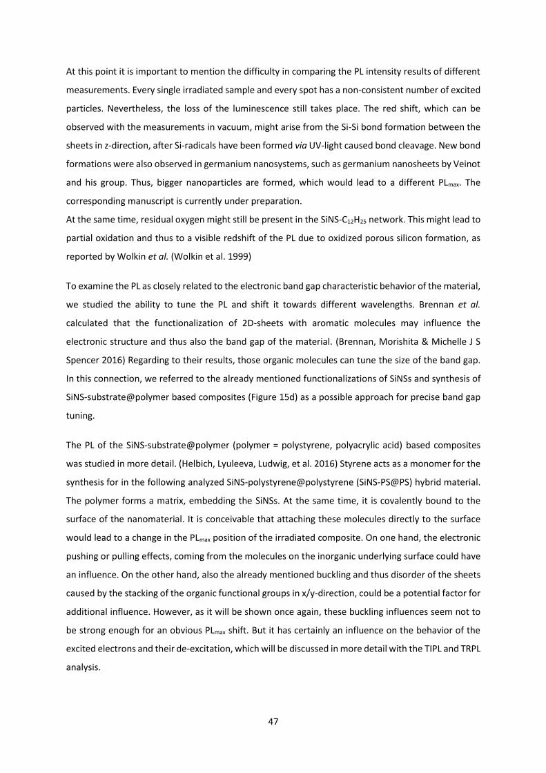
47
At this point it is important to mention the difficulty in comparing the PL intensity results of different
measurements. Every single irradiated sample and every spot has a non-consistent number of excited
particles. Nevertheless, the loss of the luminescence still takes place. The red shift, which can be
observed with the measurements in vacuum, might arise from the Si-Si bond formation between the
sheets in z-direction, after Si-radicals have been formed via UV-light caused bond cleavage. New bond
formations were also observed in germanium nanosystems, such as germanium nanosheets by Veinot
and his group. Thus, bigger nanoparticles are formed, which would lead to a different PLmax. The
corresponding manuscript is currently under preparation.
At the same time, residual oxygen might still be present in the SiNS-C12H25 network. This might lead to
partial oxidation and thus to a visible redshift of the PL due to oxidized porous silicon formation, as
reported by Wolkin et al. (Wolkin et al. 1999)
To examine the PL as closely related to the electronic band gap characteristic behavior of the material,
we studied the ability to tune the PL and shift it towards different wavelengths. Brennan et al.
calculated that the functionalization of 2D-sheets with aromatic molecules may influence the
electronic structure and thus also the band gap of the material. (Brennan, Morishita & Michelle J S
Spencer 2016) Regarding to their results, those organic molecules can tune the size of the band gap.
In this connection, we referred to the already mentioned functionalizations of SiNSs and synthesis of
SiNS-substrate@polymer based composites (Figure 15d) as a possible approach for precise band gap
tuning.
The PL of the SiNS-substrate@polymer (polymer = polystyrene, polyacrylic acid) based composites
was studied in more detail. (Helbich, Lyuleeva, Ludwig, et al. 2016) Styrene acts as a monomer for the
synthesis for in the following analyzed SiNS-polystyrene@polystyrene (SiNS-PS@PS) hybrid material.
The polymer forms a matrix, embedding the SiNSs. At the same time, it is covalently bound to the
surface of the nanomaterial. It is conceivable that attaching these molecules directly to the surface
would lead to a change in the PLmax position of the irradiated composite. On one hand, the electronic
pushing or pulling effects, coming from the molecules on the inorganic underlying surface could have
an influence. On the other hand, also the already mentioned buckling and thus disorder of the sheets
caused by the stacking of the organic functional groups in x/y-direction, could be a potential factor for
additional influence. However, as it will be shown once again, these buckling influences seem not to
be strong enough for an obvious PLmax shift. But it has certainly an influence on the behavior of the
excited electrons and their de-excitation, which will be discussed in more detail with the TIPL and TRPL
analysis.
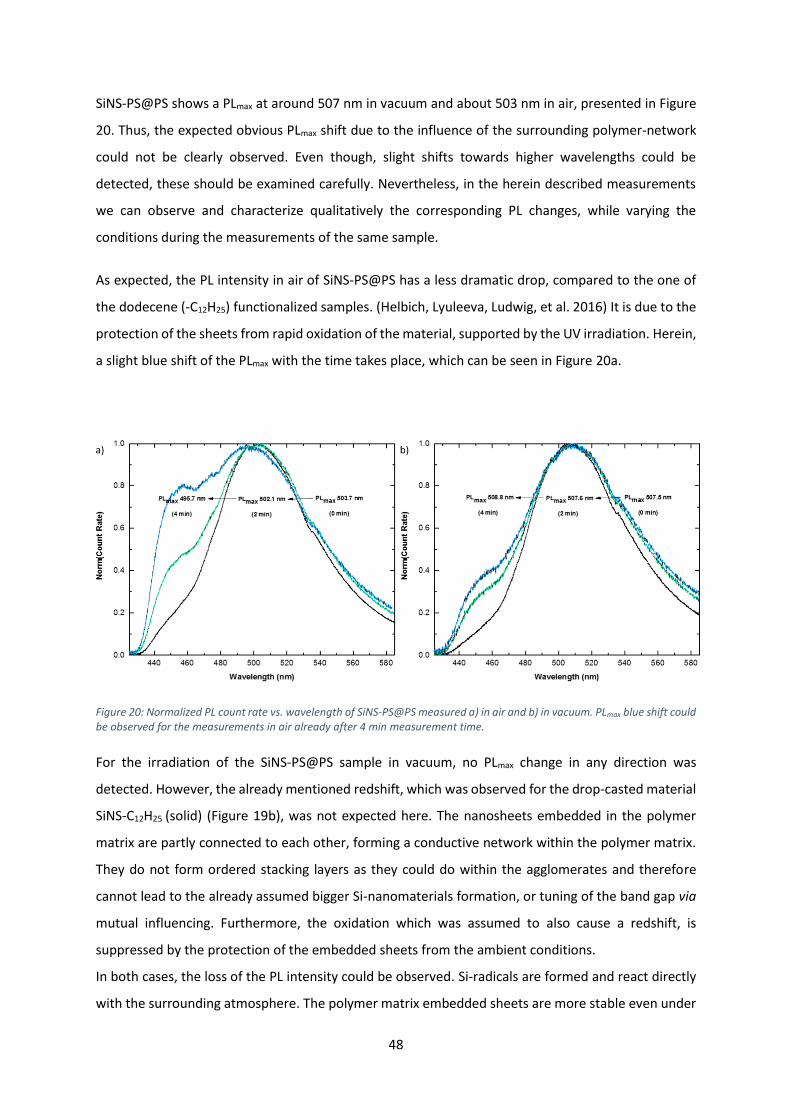
48
SiNS-PS@PS shows a PLmax at around 507 nm in vacuum and about 503 nm in air, presented in Figure
20. Thus, the expected obvious PLmax shift due to the influence of the surrounding polymer-network
could not be clearly observed. Even though, slight shifts towards higher wavelengths could be
detected, these should be examined carefully. Nevertheless, in the herein described measurements
we can observe and characterize qualitatively the corresponding PL changes, while varying the
conditions during the measurements of the same sample.
As expected, the PL intensity in air of SiNS-PS@PS has a less dramatic drop, compared to the one of
the dodecene (-C12H25) functionalized samples. (Helbich, Lyuleeva, Ludwig, et al. 2016) It is due to the
protection of the sheets from rapid oxidation of the material, supported by the UV irradiation. Herein,
a slight blue shift of the PLmax with the time takes place, which can be seen in Figure 20a.
Figure 20: Normalized PL count rate vs. wavelength of SiNS-PS@PS measured a) in air and b) in vacuum. PLmax blue shift could be observed for the measurements in air already after 4 min measurement time.
For the irradiation of the SiNS-PS@PS sample in vacuum, no PLmax change in any direction was
detected. However, the already mentioned redshift, which was observed for the drop-casted material
SiNS-C12H25 (solid) (Figure 19b), was not expected here. The nanosheets embedded in the polymer
matrix are partly connected to each other, forming a conductive network within the polymer matrix.
They do not form ordered stacking layers as they could do within the agglomerates and therefore
cannot lead to the already assumed bigger Si-nanomaterials formation, or tuning of the band gap via
mutual influencing. Furthermore, the oxidation which was assumed to also cause a redshift, is
suppressed by the protection of the embedded sheets from the ambient conditions.
In both cases, the loss of the PL intensity could be observed. Si-radicals are formed and react directly
with the surrounding atmosphere. The polymer matrix embedded sheets are more stable even under
49
direct irradiation, due to bigger possibility of the recombination reaction of two Si-radicals forming
again a Si-Si covalent bond.
These results confirm that the functional groups, which are directly bound to the SiNSs, have no
influence on the PLmax, which could be detected. Nevertheless, it is still possible to approach and to
understand the behavior of the electrons within the hybrid materials during their excitation and
relaxation processes, using for example TRPL measurement techniques. The detailed studies and
description can be additionally found in the manuscript by Lyuleeva et al. (Lyuleeva, Mary A B Narreto,
Helbich, Veinot, et al. 2017), which is currently under preparation.
This additional information about the PL can not only help to eliminate any distracting influences, but
also provide a possibility to eventually be able to tune the PL. It could be shifted to the desired range
via e.g., direct modification of the surface. The PL dynamics and behavior of other silicon-based
nanomaterials were studied by many groups in the last decade. (Nakano et al. 2005; Nakano et al.
2006; Okamoto et al. 2010; Okamoto et al. 2011; Okamoto et al. 2015; Ohshita et al. 2016) The
measurements can give information not only about the general composition, but also about the carrier
dynamics within the material and towards its interface to the surrounding system.
TRPL and TIPL spectroscopy are powerful techniques. In this connection, TRPL measurements were
carried out of the differently functionalized SiNS-substrate and SiNS-substrate@polymer composites.
The decay of the excited electrons could be detected and shows a nanosecond lifetime decay rate
(shown in Figure 21 (a)) for all functionalized SiNSs. The fit has the power law function and is universal
for every SiNSs based hybrid material studied in this work. The fit can be described with the
equation (1).
I(t)=I0+A
(bt+1)c (1)
A and b are constants, c is the power law exponent, t is time and I0 is the offset accounting for the dark
counts of the TRPL measurements. At longer times (t >> 1), I(t) ≈ t-c.
The value of the power law exponent c gives insight into the recombination processes of electrons
right after their excitation. Thus, for example c = 2 can be accounted to bio-molecular, or band-to-
band recombination processes. (Jonscher & De Polignac 1984; Pelant & Valenta 2012) 2 > c > 1 would
represent hopping mechanisms via multi-trapping of carriers. (Scher et al. 2008; Tiedje & Rose 1980)
1.5 > c > 0.95 would stand for the tunneling processes: e.g., electron traps, or random distribution of
recombination centers, whereby temperature has no effect on the system. (Huntley 2006)
50
Figure 21: a) TRPL spectrum (log-log plot) of SiNS-substrate and SiNS-substrate@polymer measured at room temperature. The solid lines represent the fit to Equation 1. b) PL of differently functionalized SiNSs measured at room temperature after excitation with ultraviolet laser (λ = 400 nm). c) Powel law exponent c vs. temperature T of differently functionalized SiNSs. The horizontal dashed line serves as guide to eye at c = 1. The green dashed line is the extrapolation of the c vs. T curve for SiNS-PAA@PAA. Adapted from Lyuleeva et al. (Lyuleeva, Mary A B Narreto, Helbich, Veinot, et al. 2017)
As already mentioned, universal fit of the decay spectra could be found, which confirms the PL of the
SiNSs coming from the band-tail recombination. The band-tail states in SiNSs are dominated by static
structural disorder of the nanomaterial. In this connection, the deviation of the power law exponent
c from the value c = 2 represents the grade of the disorder within the 2D structure. This disorder can
be caused by several aspects starting from the deintercalation of Ca2+ ions from the crystalline CaSi2
structure. Thus, already the liberation at low temperatures leading to free-standing sheets in solution
and the etching step can cause damages to the sheets and lead to defects, holes and disorder
formations. Additionally, the subsequent functionalization of the nanomaterial is carried out at
different conditions with a variety of functional groups. Every modification aspect, such as reactivity
of the unsaturated compound and of the initiator for the hydrosilylation reaction; the value and the
nature of initiating energy, applied during the reaction; additionally, the influence of the attached
1,8 2,0 2,2 2,4 2,6 2,8 3,00,0
0,2
0,4
0,6
0,8
1,0
No
rm. P
L In
ten
sity
Energy (eV)
SiNS-H
SiNS-C12H25(toluene)
SiNS-C12H25 (solid)
SiNS-PS@PS
SiNS-PAA@PAA
0,1 1 10 100
0,01
0,1
1
10
100
1.000
10.000
N
orm
. PL
Inte
nsi
ty
Time(ns)
SiNS-H(toluene)
SiNS-C12H25(toluene)
SiNS-C12H25(solid)
SiNS-PS@PS
SiNS-PAA@PAA
c = 1.44 0.02
c = 1.64 0.02
c = 0.93 0.02
c = 1.56 0.02
c = 0.96 0.02
50 100 150 200 250 3000,0
0,5
1,0
1,5
2,0
SiNS-H(toluene)
SiNS-C12H25(toluene)
SiNS-C12H25(solid)
SiNS-PS@PS
SiNS-PAA@PAA
Po
wer
law
exp
on
ent
c
Temperature (K)
(a) (b)
(c)
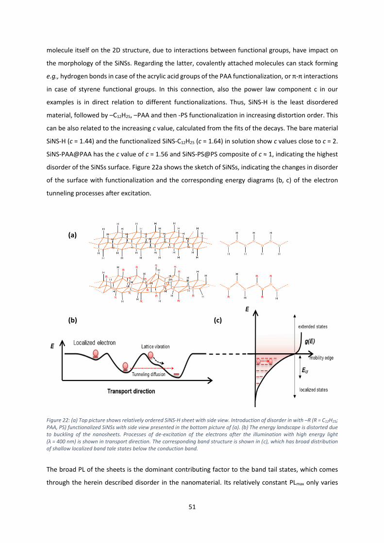
51
molecule itself on the 2D structure, due to interactions between functional groups, have impact on
the morphology of the SiNSs. Regarding the latter, covalently attached molecules can stack forming
e.g., hydrogen bonds in case of the acrylic acid groups of the PAA functionalization, or π-π interactions
in case of styrene functional groups. In this connection, also the power law component c in our
examples is in direct relation to different functionalizations. Thus, SiNS-H is the least disordered
material, followed by –C12H25, –PAA and then -PS functionalization in increasing distortion order. This
can be also related to the increasing c value, calculated from the fits of the decays. The bare material
SiNS-H (c = 1.44) and the functionalized SiNS-C12H25 (c = 1.64) in solution show c values close to c = 2.
SiNS-PAA@PAA has the c value of c = 1.56 and SiNS-PS@PS composite of c ≈ 1, indicating the highest
disorder of the SiNSs surface. Figure 22a shows the sketch of SiNSs, indicating the changes in disorder
of the surface with functionalization and the corresponding energy diagrams (b, c) of the electron
tunneling processes after excitation.
Figure 22: (a) Top picture shows relatively ordered SiNS-H sheet with side view. Introduction of disorder in with –R (R = C12H25; PAA, PS) functionalized SiNSs with side view presented in the bottom picture of (a). (b) The energy landscape is distorted due to buckling of the nanosheets. Processes of de-excitation of the electrons after the illumination with high energy light (λ = 400 nm) is shown in transport direction. The corresponding band structure is shown in (c), which has broad distribution of shallow localized band tale states below the conduction band.
The broad PL of the sheets is the dominant contributing factor to the band tail states, which comes
through the herein described disorder in the nanomaterial. Its relatively constant PLmax only varies
(a)
(b) (c)

52
from E = 2.40 eV to 2.47 eV (λ = 502 – 516 nm) regardless of the surface functionalization and is
characterized as band-like, due to the band gap opening. It is originating from the 2D Si back-bone of
the material and has broad exponential tails, attributed to the broad localized band tail states. At low
temperatures, TRPL represents tunneling charge transport and an improvement in carrier diffusion.
The rise of the PL intensity is the result.
In summary, the nature of the charge carrier transport can be well compared with the analogous
disordered semiconductors. Once again, this strengthens the ability of SiNSs to be used for
incorporation into the already established (opto)electronics in industry, which are so far based on
amorphous Si.
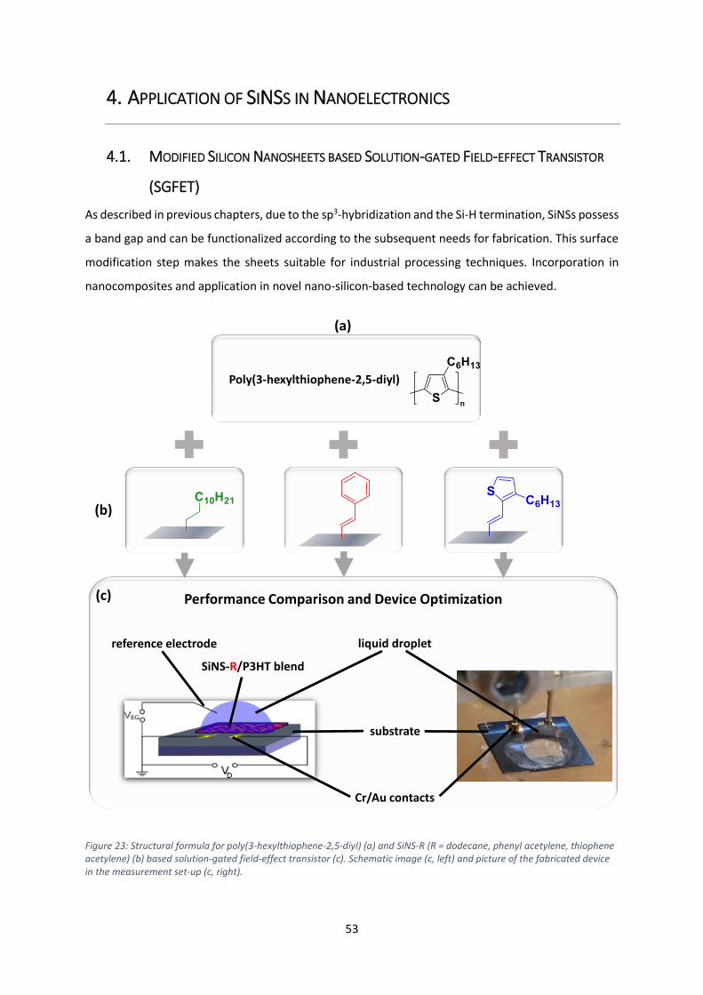
53
4. APPLICATION OF SINSS IN NANOELECTRONICS
4.1. MODIFIED SILICON NANOSHEETS BASED SOLUTION-GATED FIELD-EFFECT TRANSISTOR
(SGFET)
As described in previous chapters, due to the sp3-hybridization and the Si-H termination, SiNSs possess
a band gap and can be functionalized according to the subsequent needs for fabrication. This surface
modification step makes the sheets suitable for industrial processing techniques. Incorporation in
nanocomposites and application in novel nano-silicon-based technology can be achieved.
Figure 23: Structural formula for poly(3-hexylthiophene-2,5-diyl) (a) and SiNS-R (R = dodecane, phenyl acetylene, thiophene acetylene) (b) based solution-gated field-effect transistor (c). Schematic image (c, left) and picture of the fabricated device in the measurement set-up (c, right).
Poly(3-hexylthiophene-2,5-diyl)
(a)
(b)
Performance Comparison and Device Optimization
SiNS-R/P3HT blend
substrate
Cr/Au contacts
liquid dropletreference electrode
(c)
54
The results described in this chapter, can also be found in the corresponding submitted manuscript by
Lyuleeva et al. (Lyuleeva, Philipp Holzmüller, Helbich, Stutzmann, et al. 2017) This chapter presents
the modification of the silicane surface with specific functional groups. These organic molecules can
be covalently attached to the silicanes using a microwave-reactor system via reproducible radical-
induced hydrosilylation reaction. Subsequently, the synthesized hybrid materials are blended with the
semiconducting workhorse polymer poly(3-hexylthiophene) (P3HT), building the basis for the
solution-gated field-effect transistors (SGFETs) fabrication. To adjust the surface of the inorganic
sheets to the characteristics of the polymer for homogeneous blend formation, thiophene based
conjugated substrates are grafted on the SiNSs for improved electrical performance of the SGFETs.
4.1.1. State of the Art and Aim
Research on nanomaterials has provided an impetus for the sensing technologies on a chemical and
biomolecular level. (Kelley et al. 2014; Erickson et al. 2008; Turner 2013) In addition, FETs are a
promising tool for highly sensitive and widely applicable detection of e.g., substrates or molecules in
biological systems. (Huang et al. 2012; Liu & Guo 2012; Noor & Krull 2014) The general, mechanism of
the FET-based detection is the change in electrical conductivity of the sensitive film, induced by charge
carrier density variations or even charge transitions between the sensitive material and the
approaching molecules, which need to be detected. (Barreda et al. 2017) These occur directly on, or
near the functionalized channels of the transistor in the form of functional polarity change resulting
from external influences (Hess et al. 2014) or bond splitting/formation during chemical reactions.
(Kergoat et al. 2012; Whitener 2014) Both effects have a direct influence on the sensitivity of the
material and lead to a direct change in current, which can subsequently be detected. Additionally,
transistors provide a label free detection of surrounding targeted molecules and could be
implemented to form faster and lower-cost biomolecules detecting devices. (Leyden et al. 2010) Or,
referring to the proposed definition from the International Union of Pure and Applied Chemistry: “A
biosensor is a self-contained integrated device, which is capable of providing specific quantitative or
semi-quantitative analytical information using a biological recognition element (biochemical receptor)
which is in direct spatial contact with a transducer element”. (Ronkainen et al. 2010)
For successful applications in biological systems, the requirements such as accuracy and a high
sensitivity of the measurement need to be ensured. Furthermore, biological compatibility and work
ability of a sensor in aqueous solutions are another major aspects that must be considered when
selecting materials for use in biological sensors. In this context, the control of the materials’
properties, which are used in the sensing system, becomes once again high priority.
55
Nanomaterial-based FETs have been widely investigated. For example CNTs (Allen et al. 2007),
graphene, SiNWs (Barreda et al. 2017; Patolsky et al. 2006), TMDCs (Chow et al. 2017) and black
phosphorus (Li et al. 2014; Du et al. 2014; Yue et al. 2016) based FETs all use the capabilities that arise
when the dimensions are reduced to the nanoscale. These materials have the same goal: precisely
controlled detection and high sensitivity, based on preferably a biocompatible material, which can be
fabricated reproducibly and with low costs on even flexible substrates. However, regarding two-
dimensionality, silicon has the potential to provide all the required properties and conditions for
fabrication of a FET that is flexible, biocompatible, sensitive and controllable. Graphene, as the most
popular 2D material, provides a good foundation for consideration of 2D materials as an alternative
for post-silicon electronics. (Hess et al. 2011; Novoselov et al. 2004; Sui & Appenzeller 2009) It is highly
sensitive to its environment, allowing for the creation of a new label-free immuno-sensitive graphene
FET, which was demonstrated by Ohno et al. (Ohno et al. 2010) Nevertheless, the main issue in
graphene-based electronics arises - the intrinsic lack of a band gap. (Novoselov et al. 2004) Silicon is
an established industrial work-horse, put to use extensively in the electronics industry. Therefore,
having a 2D silicon-based FET would be a highly attractive solution for these limitations that arise in
bulk silicon. (Lu et al. 2012) However, as already mentioned, 2D silicon such as silicene and layered
polysilane, lack stability, due to the ability to easily undergo oxidation reactions that form a glass-like
α-SiOx phase (Dahn et al. 1993) under ambient conditions and influence of UV light. (Helbich, Lyuleeva,
Höhlein, et al. 2016; Helbich, Lyuleeva, Ludwig, et al. 2016) This requires encapsulation, using either
composite synthesis, or covalent functionalization, which was already described in chapter 1.2.
Additionally, the already mentioned ease of fabrication and assured sensing performance needs to be
established. Resulting from that, P3HT as a well-known semiconducting polymer (Liao & Yan 2013)
was considered for the use in combination with 2D SiNSs. One of the main advantages of the blend
formation is the ease of the subsequent thin film fabrication, which becomes a well-controlled and
reproducible fabrication step. Furthermore, blends also allow for non-destructive combination of both
materials’ properties, which eventually lead to the improvement in the performance of the device.
The implementation of a nanomaterial such as CNTs (Rubin et al. 2002) or graphene (Sun & Wang
2007) within the active area of the device was shown to lead to a significant improvement of its
sensitivity. The combination of functionalized SiNSs with P3HT was not only used to embed the
inorganic nanomaterial and thus increase its stability, but it also facilitated the fabrication and
improved the sensitivity of the desired FETs as well.
4.1.2. Results and Discussion
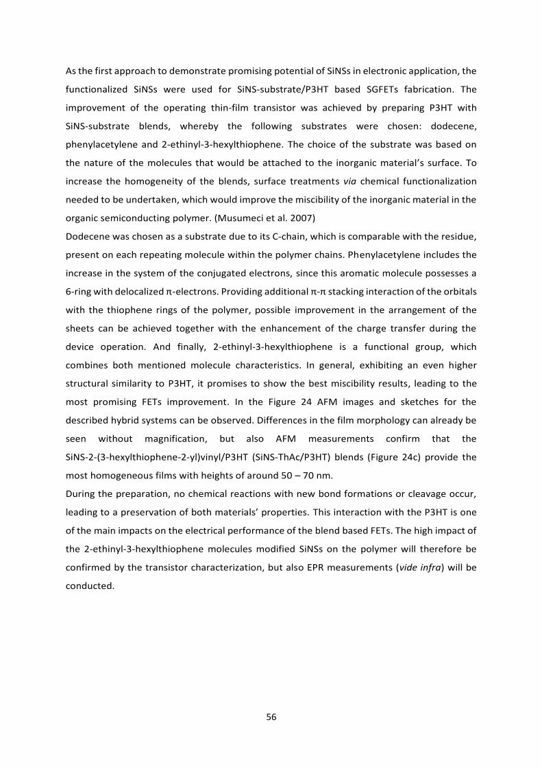
56
As the first approach to demonstrate promising potential of SiNSs in electronic application, the
functionalized SiNSs were used for SiNS-substrate/P3HT based SGFETs fabrication. The
improvement of the operating thin-film transistor was achieved by preparing P3HT with
SiNS-substrate blends, whereby the following substrates were chosen: dodecene,
phenylacetylene and 2-ethinyl-3-hexylthiophene. The choice of the substrate was based on
the nature of the molecules that would be attached to the inorganic material’s surface. To
increase the homogeneity of the blends, surface treatments via chemical functionalization
needed to be undertaken, which would improve the miscibility of the inorganic material in the
organic semiconducting polymer. (Musumeci et al. 2007)
Dodecene was chosen as a substrate due to its C-chain, which is comparable with the residue,
present on each repeating molecule within the polymer chains. Phenylacetylene includes the
increase in the system of the conjugated electrons, since this aromatic molecule possesses a
6-ring with delocalized π-electrons. Providing additional π-π stacking interaction of the orbitals
with the thiophene rings of the polymer, possible improvement in the arrangement of the
sheets can be achieved together with the enhancement of the charge transfer during the
device operation. And finally, 2-ethinyl-3-hexylthiophene is a functional group, which
combines both mentioned molecule characteristics. In general, exhibiting an even higher
structural similarity to P3HT, it promises to show the best miscibility results, leading to the
most promising FETs improvement. In the Figure 24 AFM images and sketches for the
described hybrid systems can be observed. Differences in the film morphology can already be
seen without magnification, but also AFM measurements confirm that the
SiNS-2-(3-hexylthiophene-2-yl)vinyl/P3HT (SiNS-ThAc/P3HT) blends (Figure 24c) provide the
most homogeneous films with heights of around 50 – 70 nm.
During the preparation, no chemical reactions with new bond formations or cleavage occur,
leading to a preservation of both materials’ properties. This interaction with the P3HT is one
of the main impacts on the electrical performance of the blend based FETs. The high impact of
the 2-ethinyl-3-hexylthiophene molecules modified SiNSs on the polymer will therefore be
confirmed by the transistor characterization, but also EPR measurements (vide infra) will be
conducted.
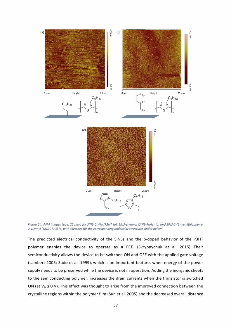
57
Figure 24: AFM images (size: 25 µm2) for SiNS-C12H25/P3HT (a), SiNS-styrenyl (SiNS-PhAc) (b) and SiNS-2-(3-hexylthiophene-2-yl)vinyl (SiNS-ThAc) (c) with sketches for the corresponding molecular structures under below.
The predicted electrical conductivity of the SiNSs and the p-doped behavior of the P3HT
polymer enables the device to operate as a FET. (Skrypnychuk et al. 2015) Their
semiconductivity allows the device to be switched ON and OFF with the applied gate voltage
(Lambert 2005; Sudo et al. 1999), which is an important feature, when energy of the power
supply needs to be preserved while the device is not in operation. Adding the inorganic sheets
to the semiconducting polymer, increases the drain currents when the transistor is switched
ON (at VG ≤ 0 V). This effect was thought to arise from the improved connection between the
crystalline regions within the polymer film (Sun et al. 2005) and the decreased overall distance
0 µm Height 25 µm
0 µm Height 25 µm 0 µm Height 25 µm
(a) (b)
(c)
-3.7
nm
4.9
nm
4.7
nm
-4.2
nm
5.4
nm
-4.9
nm
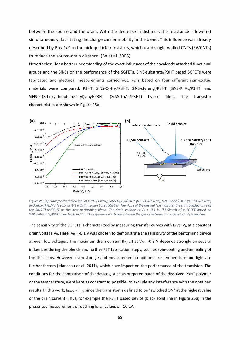
58
between the source and the drain. With the decrease in distance, the resistance is lowered
simultaneously, facilitating the charge carrier mobility in the blend. This influence was already
described by Bo et al. in the pickup stick transistors, which used single-walled CNTs (SWCNTs)
to reduce the source-drain distance. (Bo et al. 2005)
Nevertheless, for a better understanding of the exact influences of the covalently attached functional
groups and the SiNSs on the performance of the SGFETs, SiNS-substrate/P3HT based SGFETs were
fabricated and electrical measurements carried out. FETs based on four different spin-coated
materials were compared: P3HT, SiNS-C12H25/P3HT, SiNS-styrenyl/P3HT (SiNS-PhAc/P3HT) and
SiNS-2-(3-hexylthiophene-2-yl)vinyl/P3HT (SiNS-ThAc/P3HT) hybrid films. The transistor
characteristics are shown in Figure 25a.
Figure 25: (a) Transfer characteristics of P3HT (1 wt%), SiNS-C12H25/P3HT (0.5 wt%/1 wt%), SiNS-PhAc/P3HT (0.5 wt%/1 wt%) and SiNS-ThAc/P3HT (0.5 wt%/1 wt%) thin-film based SGFETs. The slope of the dashed line indicates the transconductance of the SiNS-ThAc/P3HT as the best performing blend. The drain voltage is VD = -0.1 V. (b) Sketch of a SGFET based on SiNS-substrate/P3HT blended thin film. The reference electrode is herein the gate electrode, through which VG is applied.
The sensitivity of the SGFETs is characterized by measuring transfer curves with ID vs. VG at a constant
drain voltage VD. Here, VD = -0.1 V was chosen to demonstrate the sensitivity of the performing device
at even low voltages. The maximum drain current (ID,max) at VG = -0.8 V depends strongly on several
influences during the blends and further FET fabrication steps, such as spin-coating and annealing of
the thin films. However, even storage and measurement conditions like temperature and light are
further factors (Manceau et al. 2011), which have impact on the performance of the transistor. The
conditions for the comparison of the devices, such as prepared batch of the dissolved P3HT polymer
or the temperature, were kept as constant as possible, to exclude any interference with the obtained
results. In this work, ID,max = ION, since the transistor is defined to be “switched ON” at the highest value
of the drain current. Thus, for example the P3HT based device (black solid line in Figure 25a) in the
presented measurement is reaching ID,max values of -10 µA.
-0,8 -0,6 -0,4 -0,2 0,0 0,2 0,4 0,6 0,8-4,5x10⁻⁵
-4,0x10⁻⁵
-3,5x10⁻⁵
-3,0x10⁻⁵
-2,5x10⁻⁵
-2,0x10⁻⁵
-1,5x10⁻⁵
-1,0x10⁻⁵
-5,0x10⁻⁶
0,0
Dra
in I D
in A
Gate VG in V
P3HT (1 wt%)
P3HT/Si-NS-C12H25 (1 wt%, 0.5 wt%)
P3HT/Si-NS-PhAc (1 wt%, 0.5 wt%)
P3HT/Si-NS-ThAc (1 wt%, 0.5 wt%)
slope = transconductance
substrate
SiNS-substrate/P3HT thin film
Cr/Au contacts
liquid dropletreference electrode(a) (b)
59
After adding the SiNS-substrate to the polymer, the resulting SGFETs show significantly increased drain
currents. As already discussed and expected, with the influence of the functionalization this increase
in current shows the following order, going from the least to the best performing blend: SiNS-C12H25
(ION = 17.5 µA) < SiNS-PhAc (ION = 22.5 µA) < SiNS-ThAc (ION = 40 µA). The dodecene functionalized
nanosheets could introduce disorder into the polymeric system, which is less likely present in the
blend with the ThAc functionalized sheets (for further analysis see Grazing-Incidence Wide-Angle X-
Ray Scattering (GIWAXS) Measurements in the appendix). In addition, the dodecene chains do not
form stacking structures with the aromatic rings of the P3HT polymer, which might be useful for the
charge transfer and thus increase the mobility in the film. (Urien et al. 2007; Brinkmann & Rannou
2007; Machui 2014) Another issue, arising with the SiNS-C12H25 blends, is the increased OFF current
(IOFF) at gate voltages of about VG ≥ 0.4 V. While the ON current is increased, the OFF current is also
significantly shifted towards higher values. This effect lowers the ON/OFF ratio of the device and thus
the sensitivity of its performance. Also, the SiNS-PhAc based blends show comparable shift of the IOFF,
resulting in the ON/OFF ratio of ION/IOFF = 17.4. The reason could be either the inhomogeneity of the
film, or the agglomerates of the sheets, which might form due to insufficient mixing with the polymer
and subsequent accumulation of the sheets on the bottom of the thin film. These stacking structures
can build occasional parts in the channel with lower resistances, allowing currents to flow even when
the transistor is turned OFF. As already mentioned, keeping the OFF current as low as possible when
the device is not in operation, is valuable when it comes to the extension of the lifetime of the power
supply and use in low-power applications.
Finally, the best performing blend is based on SiNS-ThAc mixed with P3HT. The OFF currents in this
device were kept in the range of bare P3HT, at the same time ION reaches nearly 4 times higher values.
(Figure 26a) The transconductance (gm) of the device is defined by the slope of the ID/VG curve and
reaches the value of 4.98 ∙ 10-5 A/V being automatically enhanced. This improvement is directly related
to the sensitivity of the device, since it shows how much current change can occur at a certain change
of the voltage. These measurements show that the ThAc functionalization evokes the best
characteristics of the herby presented p-type transistors. For that reason, also the output
characteristics were performed to complete the characterization of a transistor, showing for a p-
semiconductor typical shape of the curves, while negative voltages were applied (Figure 26b). These
results confirm the miscibility influence on the device performance and can pave the way towards
new and promising solutions, which can help to face related issues in surface engineering and charge
interaction control of the material.
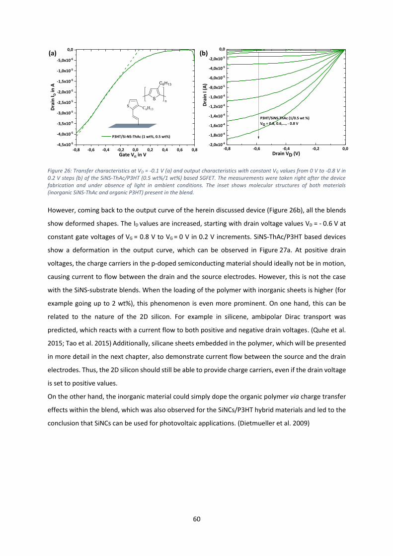
60
Figure 26: Transfer characteristics at VD = -0.1 V (a) and output characteristics with constant VG values from 0 V to -0.8 V in 0.2 V steps (b) of the SiNS-ThAc/P3HT (0.5 wt%/1 wt%) based SGFET. The measurements were taken right after the device fabrication and under absence of light in ambient conditions. The inset shows molecular structures of both materials (inorganic SiNS-ThAc and organic P3HT) present in the blend.
However, coming back to the output curve of the herein discussed device (Figure 26b), all the blends
show deformed shapes. The ID values are increased, starting with drain voltage values VD = - 0.6 V at
constant gate voltages of VG = 0.8 V to VG = 0 V in 0.2 V increments. SiNS-ThAc/P3HT based devices
show a deformation in the output curve, which can be observed in Figure 27a. At positive drain
voltages, the charge carriers in the p-doped semiconducting material should ideally not be in motion,
causing current to flow between the drain and the source electrodes. However, this is not the case
with the SiNS-substrate blends. When the loading of the polymer with inorganic sheets is higher (for
example going up to 2 wt%), this phenomenon is even more prominent. On one hand, this can be
related to the nature of the 2D silicon. For example in silicene, ambipolar Dirac transport was
predicted, which reacts with a current flow to both positive and negative drain voltages. (Quhe et al.
2015; Tao et al. 2015) Additionally, silicane sheets embedded in the polymer, which will be presented
in more detail in the next chapter, also demonstrate current flow between the source and the drain
electrodes. Thus, the 2D silicon should still be able to provide charge carriers, even if the drain voltage
is set to positive values.
On the other hand, the inorganic material could simply dope the organic polymer via charge transfer
effects within the blend, which was also observed for the SiNCs/P3HT hybrid materials and led to the
conclusion that SiNCs can be used for photovoltaic applications. (Dietmueller et al. 2009)
-0,8 -0,6 -0,4 -0,2 0,0 0,2 0,4 0,6 0,8-4,5x10⁻⁵
-4,0x10⁻⁵
-3,5x10⁻⁵
-3,0x10⁻⁵
-2,5x10⁻⁵
-2,0x10⁻⁵
-1,5x10⁻⁵
-1,0x10⁻⁵
-5,0x10⁻⁶
0,0D
rain
I D in
A
Gate VG in V
P3HT/Si-NS-ThAc (1 wt%, 0.5 wt%)
(a)
-0,8 -0,6 -0,4 -0,2 0,0-2,0x10⁻⁴
-1,8x10⁻⁴
-1,6x10⁻⁴
-1,4x10⁻⁴
-1,2x10⁻⁴
-1,0x10⁻⁴
-8,0x10⁻⁵
-6,0x10⁻⁵
-4,0x10⁻⁵
-2,0x10⁻⁵
0,0
Dra
in I
(A)
Drain VD (V)
P3HT/SiNS-ThAc (1/0.5 wt %)
VG = 0.8, 0.6,..., - 0.8 V
(b)
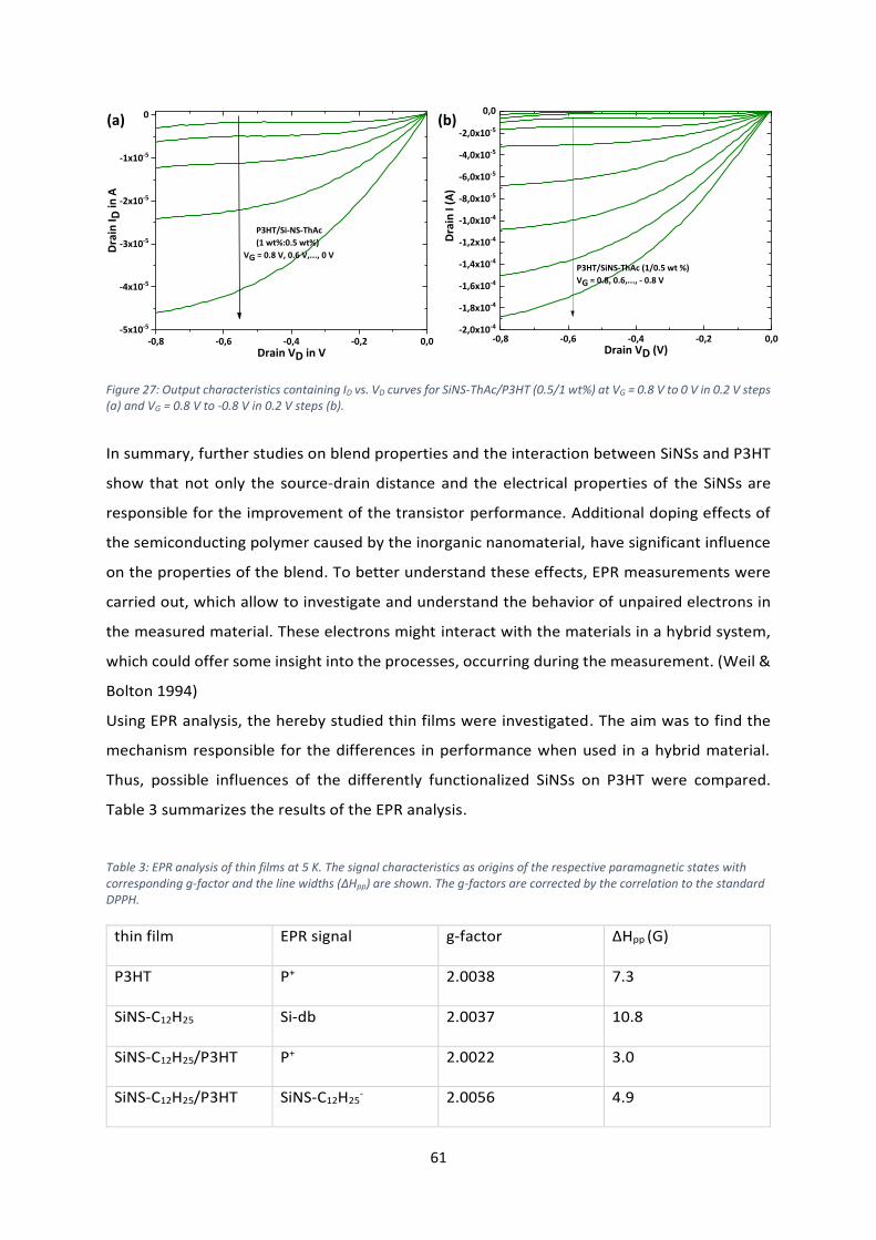
61
Figure 27: Output characteristics containing ID vs. VD curves for SiNS-ThAc/P3HT (0.5/1 wt%) at VG = 0.8 V to 0 V in 0.2 V steps (a) and VG = 0.8 V to -0.8 V in 0.2 V steps (b).
In summary, further studies on blend properties and the interaction between SiNSs and P3HT
show that not only the source-drain distance and the electrical properties of the SiNSs are
responsible for the improvement of the transistor performance. Additional doping effects of
the semiconducting polymer caused by the inorganic nanomaterial, have significant influence
on the properties of the blend. To better understand these effects, EPR measurements were
carried out, which allow to investigate and understand the behavior of unpaired electrons in
the measured material. These electrons might interact with the materials in a hybrid system,
which could offer some insight into the processes, occurring during the measurement. (Weil &
Bolton 1994)
Using EPR analysis, the hereby studied thin films were investigated. The aim was to find the
mechanism responsible for the differences in performance when used in a hybrid material.
Thus, possible influences of the differently functionalized SiNSs on P3HT were compared.
Table 3 summarizes the results of the EPR analysis.
Table 3: EPR analysis of thin films at 5 K. The signal characteristics as origins of the respective paramagnetic states with corresponding g-factor and the line widths (∆Hpp) are shown. The g-factors are corrected by the correlation to the standard DPPH.
thin film EPR signal g-factor ∆Hpp (G)
P3HT P+ 2.0038 7.3
SiNS-C12H25 Si-db 2.0037 10.8
SiNS-C12H25/P3HT P+ 2.0022 3.0
SiNS-C12H25/P3HT SiNS-C12H25- 2.0056 4.9
-0,8 -0,6 -0,4 -0,2 0,0-5x10⁻⁵
-4x10⁻⁵
-3x10⁻⁵
-2x10⁻⁵
-1x10⁻⁵
0
P3HT/Si-NS-ThAc
(1 wt%:0.5 wt%)
VG = 0.8 V, 0.6 V,..., 0 V
Dra
in I D
in A
Drain VD in V
(a)
-0,8 -0,6 -0,4 -0,2 0,0-2,0x10⁻⁴
-1,8x10⁻⁴
-1,6x10⁻⁴
-1,4x10⁻⁴
-1,2x10⁻⁴
-1,0x10⁻⁴
-8,0x10⁻⁵
-6,0x10⁻⁵
-4,0x10⁻⁵
-2,0x10⁻⁵
0,0
Dra
in I
(A)
Drain VD (V)
P3HT/SiNS-ThAc (1/0.5 wt %)
VG = 0.8, 0.6,..., - 0.8 V
(b)
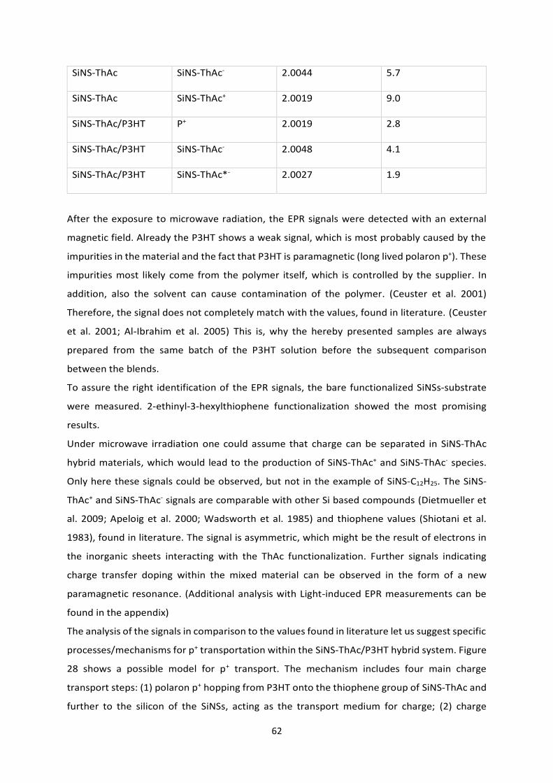
62
SiNS-ThAc SiNS-ThAc- 2.0044 5.7
SiNS-ThAc SiNS-ThAc+ 2.0019 9.0
SiNS-ThAc/P3HT P+ 2.0019 2.8
SiNS-ThAc/P3HT SiNS-ThAc- 2.0048 4.1
SiNS-ThAc/P3HT SiNS-ThAc*- 2.0027 1.9
After the exposure to microwave radiation, the EPR signals were detected with an external
magnetic field. Already the P3HT shows a weak signal, which is most probably caused by the
impurities in the material and the fact that P3HT is paramagnetic (long lived polaron p+). These
impurities most likely come from the polymer itself, which is controlled by the supplier. In
addition, also the solvent can cause contamination of the polymer. (Ceuster et al. 2001)
Therefore, the signal does not completely match with the values, found in literature. (Ceuster
et al. 2001; Al-Ibrahim et al. 2005) This is, why the hereby presented samples are always
prepared from the same batch of the P3HT solution before the subsequent comparison
between the blends.
To assure the right identification of the EPR signals, the bare functionalized SiNSs-substrate
were measured. 2-ethinyl-3-hexylthiophene functionalization showed the most promising
results.
Under microwave irradiation one could assume that charge can be separated in SiNS-ThAc
hybrid materials, which would lead to the production of SiNS-ThAc+ and SiNS-ThAc- species.
Only here these signals could be observed, but not in the example of SiNS-C12H25. The SiNS-
ThAc+ and SiNS-ThAc- signals are comparable with other Si based compounds (Dietmueller et
al. 2009; Apeloig et al. 2000; Wadsworth et al. 1985) and thiophene values (Shiotani et al.
1983), found in literature. The signal is asymmetric, which might be the result of electrons in
the inorganic sheets interacting with the ThAc functionalization. Further signals indicating
charge transfer doping within the mixed material can be observed in the form of a new
paramagnetic resonance. (Additional analysis with Light-induced EPR measurements can be
found in the appendix)
The analysis of the signals in comparison to the values found in literature let us suggest specific
processes/mechanisms for p+ transportation within the SiNS-ThAc/P3HT hybrid system. Figure
28 shows a possible model for p+ transport. The mechanism includes four main charge
transport steps: (1) polaron p+ hopping from P3HT onto the thiophene group of SiNS-ThAc and
further to the silicon of the SiNSs, acting as the transport medium for charge; (2) charge
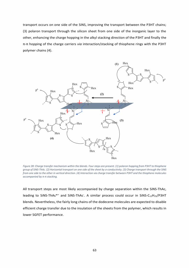
63
transport occurs on one side of the SiNS, improving the transport between the P3HT chains;
(3) polaron transport through the silicon sheet from one side of the inorganic layer to the
other, enhancing the charge hopping in the alkyl stacking direction of the P3HT and finally the
π-π hopping of the charge carriers via interaction/stacking of thiophene rings with the P3HT
polymer chains (4).
Figure 28: Charge transfer mechanism within the blends. Four steps are present. (1) polaron hopping from P3HT to thiophene group of SiNS-ThAc. (2) Horizontal transport on one side of the sheet by σ-conductivity. (3) Charge transport through the SINS from one side to the other in vertical direction. (4) Interaction via charge transfer between P3HT and the thiophene molecules accompanied by π-π stacking.
All transport steps are most likely accompanied by charge separation within the SiNS-ThAc,
leading to SiNS-ThAc*+ and SiNS-ThAc-. A similar process could occur in SiNS-C12H25/P3HT
blends. Nevertheless, the fairly long chains of the dodecene molecules are expected to disable
efficient charge transfer due to the insulation of the sheets from the polymer, which results in
lower SGFET performance.
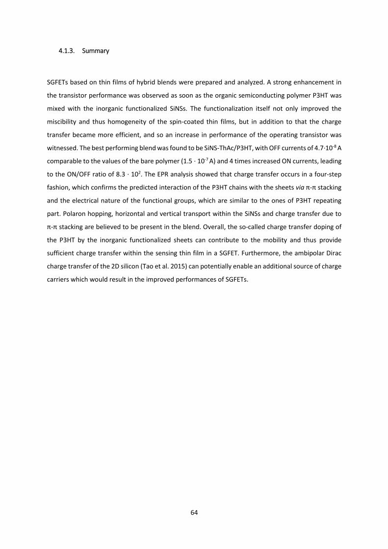
64
4.1.3. Summary
SGFETs based on thin films of hybrid blends were prepared and analyzed. A strong enhancement in
the transistor performance was observed as soon as the organic semiconducting polymer P3HT was
mixed with the inorganic functionalized SiNSs. The functionalization itself not only improved the
miscibility and thus homogeneity of the spin-coated thin films, but in addition to that the charge
transfer became more efficient, and so an increase in performance of the operating transistor was
witnessed. The best performing blend was found to be SiNS-ThAc/P3HT, with OFF currents of 4.7∙10-8 A
comparable to the values of the bare polymer (1.5 ∙ 10-7 A) and 4 times increased ON currents, leading
to the ON/OFF ratio of 8.3 ∙ 102. The EPR analysis showed that charge transfer occurs in a four-step
fashion, which confirms the predicted interaction of the P3HT chains with the sheets via π-π stacking
and the electrical nature of the functional groups, which are similar to the ones of P3HT repeating
part. Polaron hopping, horizontal and vertical transport within the SiNSs and charge transfer due to
π-π stacking are believed to be present in the blend. Overall, the so-called charge transfer doping of
the P3HT by the inorganic functionalized sheets can contribute to the mobility and thus provide
sufficient charge transfer within the sensing thin film in a SGFET. Furthermore, the ambipolar Dirac
charge transfer of the 2D silicon (Tao et al. 2015) can potentially enable an additional source of charge
carriers which would result in the improved performances of SGFETs.
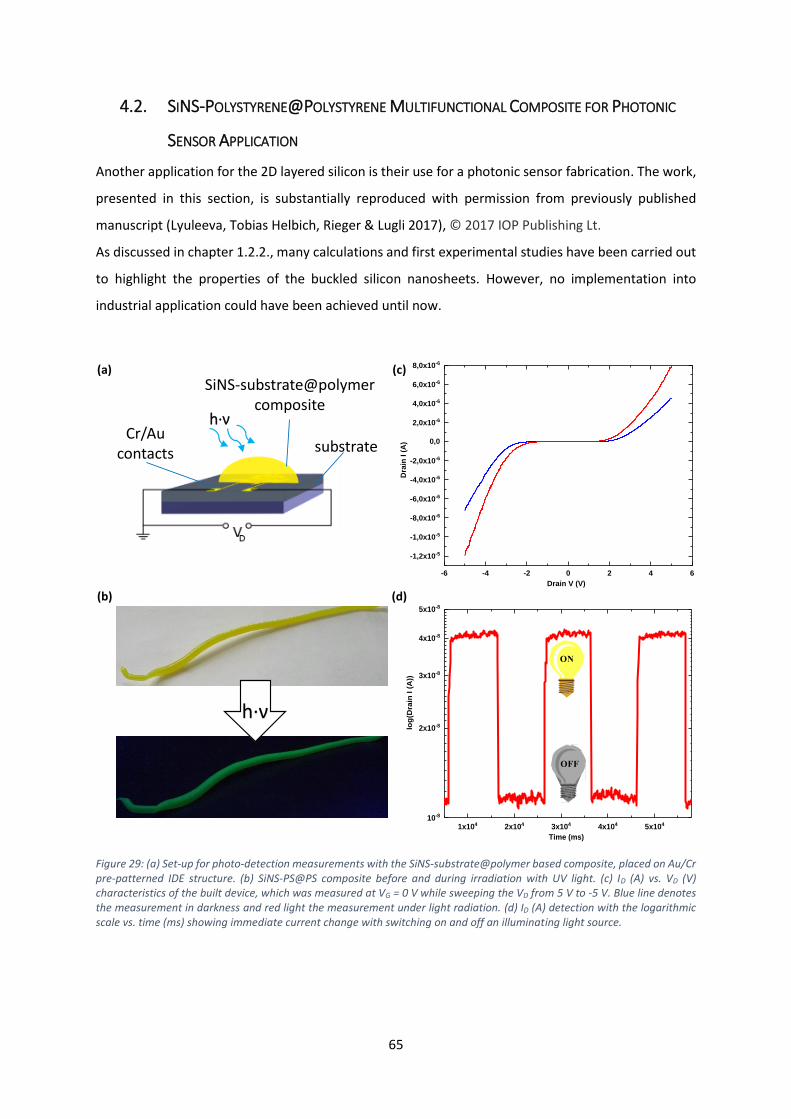
65
4.2. SINS-POLYSTYRENE@POLYSTYRENE MULTIFUNCTIONAL COMPOSITE FOR PHOTONIC
SENSOR APPLICATION
Another application for the 2D layered silicon is their use for a photonic sensor fabrication. The work,
presented in this section, is substantially reproduced with permission from previously published
manuscript (Lyuleeva, Tobias Helbich, Rieger & Lugli 2017), © 2017 IOP Publishing Lt.
As discussed in chapter 1.2.2., many calculations and first experimental studies have been carried out
to highlight the properties of the buckled silicon nanosheets. However, no implementation into
industrial application could have been achieved until now.
Figure 29: (a) Set-up for photo-detection measurements with the SiNS-substrate@polymer based composite, placed on Au/Cr pre-patterned IDE structure. (b) SiNS-PS@PS composite before and during irradiation with UV light. (c) ID (A) vs. VD (V) characteristics of the built device, which was measured at VG = 0 V while sweeping the VD from 5 V to -5 V. Blue line denotes the measurement in darkness and red light the measurement under light radiation. (d) ID (A) detection with the logarithmic scale vs. time (ms) showing immediate current change with switching on and off an illuminating light source.
h·ν
substrate
SiNS-substrate@polymercomposite
Cr/Au contacts
-6 -4 -2 0 2 4 6
-1,2x10⁻⁵
-1,0x10⁻⁵
-8,0x10⁻⁶
-6,0x10⁻⁶
-4,0x10⁻⁶
-2,0x10⁻⁶
0,0
2,0x10⁻⁶
4,0x10⁻⁶
6,0x10⁻⁶
8,0x10⁻⁶
Dra
in I (
A)
Drain V (V)
1x10⁴ 2x10⁴ 3x10⁴ 4x10⁴ 5x10410-8
2x10⁻⁸
3x10⁻⁸
4x10⁻⁸
5x10⁻⁸
log
(Dra
in I
(A
))
Time (ms)
(a)
(b)
(c)
(d)
h·ν
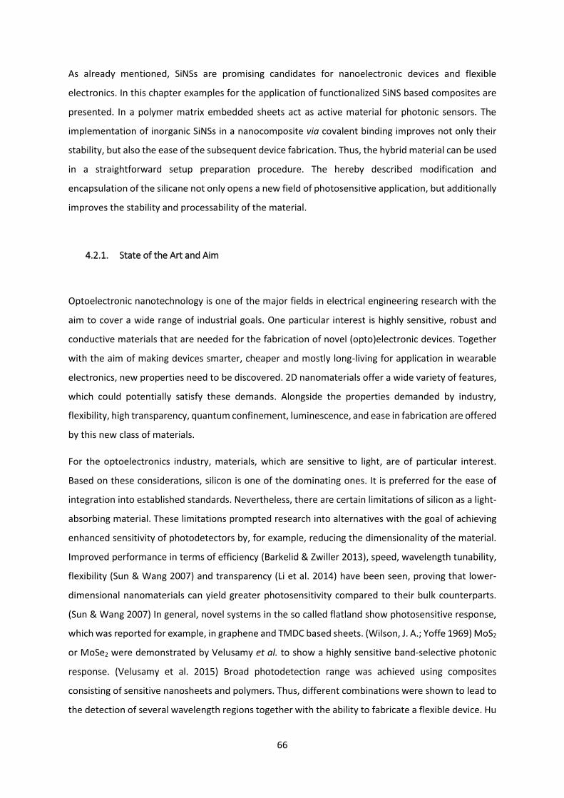
66
As already mentioned, SiNSs are promising candidates for nanoelectronic devices and flexible
electronics. In this chapter examples for the application of functionalized SiNS based composites are
presented. In a polymer matrix embedded sheets act as active material for photonic sensors. The
implementation of inorganic SiNSs in a nanocomposite via covalent binding improves not only their
stability, but also the ease of the subsequent device fabrication. Thus, the hybrid material can be used
in a straightforward setup preparation procedure. The hereby described modification and
encapsulation of the silicane not only opens a new field of photosensitive application, but additionally
improves the stability and processability of the material.
4.2.1. State of the Art and Aim
Optoelectronic nanotechnology is one of the major fields in electrical engineering research with the
aim to cover a wide range of industrial goals. One particular interest is highly sensitive, robust and
conductive materials that are needed for the fabrication of novel (opto)electronic devices. Together
with the aim of making devices smarter, cheaper and mostly long-living for application in wearable
electronics, new properties need to be discovered. 2D nanomaterials offer a wide variety of features,
which could potentially satisfy these demands. Alongside the properties demanded by industry,
flexibility, high transparency, quantum confinement, luminescence, and ease in fabrication are offered
by this new class of materials.
For the optoelectronics industry, materials, which are sensitive to light, are of particular interest.
Based on these considerations, silicon is one of the dominating ones. It is preferred for the ease of
integration into established standards. Nevertheless, there are certain limitations of silicon as a light-
absorbing material. These limitations prompted research into alternatives with the goal of achieving
enhanced sensitivity of photodetectors by, for example, reducing the dimensionality of the material.
Improved performance in terms of efficiency (Barkelid & Zwiller 2013), speed, wavelength tunability,
flexibility (Sun & Wang 2007) and transparency (Li et al. 2014) have been seen, proving that lower-
dimensional nanomaterials can yield greater photosensitivity compared to their bulk counterparts.
(Sun & Wang 2007) In general, novel systems in the so called flatland show photosensitive response,
which was reported for example, in graphene and TMDC based sheets. (Wilson, J. A.; Yoffe 1969) MoS2
or MoSe2 were demonstrated by Velusamy et al. to show a highly sensitive band-selective photonic
response. (Velusamy et al. 2015) Broad photodetection range was achieved using composites
consisting of sensitive nanosheets and polymers. Thus, different combinations were shown to lead to
the detection of several wavelength regions together with the ability to fabricate a flexible device. Hu

67
et al. succeeded in building a photonic sensor based on 2D materials, namely GaS nanosheets. (Hu et
al. 2013) Their device was placed on a rigid Si++/SiO2 substrate and can be used for the detection across
UV and visible regions. All together, these achievements encourage research in silicon-based science
to find a suitable approach for the fabrication of 2D silicon-based photonic sensors.
This is where 2D SiNSs have much to offer. Sugiyama et al. confirmed in 2010 that 2D silicon is suitable
for photonic sensor applications after detecting light-induced photocurrent using a three-electrode
photo-electrochemical cell. (Sugiyama, Okamoto, Mitsuoka, et al. 2010) After modification of the
nanomaterial, a current could be generated. For example, modifying the SiNSs with phenyl groups
produced wavelength-dependent currents which could be generated using wavelengths below 410
nm. (Sugiyama, Okamoto, Mitsuoka, et al. 2010) This indicates photo-excited current generation via a
band gap transition. (Koski & Cui 2013; Ohshita et al. 2016)
Nevertheless, despite these successful results, Sugiyama and co-workers demonstrated a lack of
stability of freestanding SiNSs, which are sensitive to external influences such as oxygen in air. Our
work also confirmed this instability. (Helbich, Lyuleeva, Höhlein, et al. 2016) Additionally, as already
mentioned, SiNSs possess a high surface-to-volume ratio and thus tend to agglomerate easily, which
requires additional modification to ensure dispersion in organic solvents. (Sugiyama, Okamoto,
Mitsuoka, et al. 2010) Therefore, the stabilization via surface modification plays a significant role and
as it will be demonstrated in the following section that covalently bound composites can be
synthesized, which preserve both materials properties. Thus, with this nanocomposite the processing
properties of the polymers with the (opto)electronic characteristics of the SiNSs were combined for
the fabrication of a light-sensitive device.
4.2.2. Results and Discussion
As already mentioned, the herein studied silicane sheets have a band gap of about 2.4 – 2.45 eV, which
leads to a green PL at around 510 nm of the material. (Tao et al. 2015; Nakano 2014; Niu et al. 2014)
The sheets can be illuminated with UV light, which forces the charge carriers to jump into excited
states and subsequently return to their original energy value by emitting photons. This causes
photoluminescence, which in the case of SiNSs is in the visible range. Additionally, to confirm once
again, the SiNSs have a height of about 5 nm, whereby stacking layers can be detected with the AFM
imaging. An AFM image of freshly exfoliated SiNSs is shown in Figure 30.
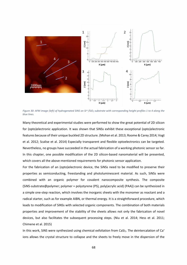
68
Figure 30: AFM image (left) of hydrogenated SINS on SI++/SiO2 substrate with corresponding height profiles 1 to 4 along the blue lines.
Many theoretical and experimental studies were performed to show the great potential of 2D silicon
for (opto)electronic application. It was shown that SiNSs exhibit these exceptional (opto)electronic
features because of their unique buckled 2D structure. (Mohan et al. 2013; Roome & Carey 2014; Vogt
et al. 2012; Scalise et al. 2014) Especially transparent and flexible optoelectronics can be targeted.
Nevertheless, no groups have succeeded in the actual fabrication of a working photonic sensor so far.
In this chapter, one possible modification of the 2D silicon-based nanomaterial will be presented,
which covers all the above-mentioned requirements for photonic sensor application.
For the fabrication of an (opto)electronic device, the SiNSs need to be modified to preserve their
properties as semiconducting, freestanding and photoluminescent material. As such, SiNSs were
combined with an organic polymer for covalent nanocomposite synthesis. The composite
(SiNS-substrate@polymer; polymer = polystyrene (PS), poly(acrylic acid) (PAA)) can be synthesized in
a simple one-step reaction, which involves the inorganic sheets with the monomer as reactant and a
radical starter, such as for example AIBN, or thermal energy. It is a straightforward procedure, which
leads to modification of SiNSs with selected organic components. The combination of both materials
properties and improvement of the stability of the sheets allows not only the fabrication of novel
devices, but also facilitates the subsequent processing steps. (Niu et al. 2014; Hess et al. 2011;
Chimene et al. 2015)
In this work, SiNS were synthesized using chemical exfoliation from CaSi2. The deintercalation of Ca+
ions allows the crystal structure to collapse and the sheets to freely move in the dispersion of the
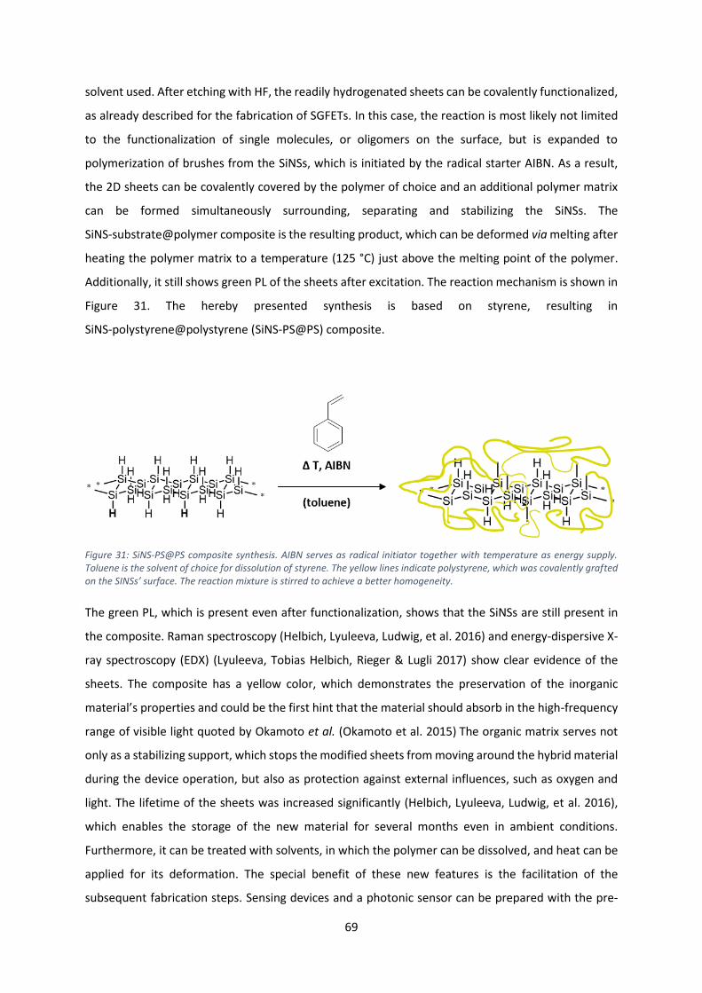
69
solvent used. After etching with HF, the readily hydrogenated sheets can be covalently functionalized,
as already described for the fabrication of SGFETs. In this case, the reaction is most likely not limited
to the functionalization of single molecules, or oligomers on the surface, but is expanded to
polymerization of brushes from the SiNSs, which is initiated by the radical starter AIBN. As a result,
the 2D sheets can be covalently covered by the polymer of choice and an additional polymer matrix
can be formed simultaneously surrounding, separating and stabilizing the SiNSs. The
SiNS-substrate@polymer composite is the resulting product, which can be deformed via melting after
heating the polymer matrix to a temperature (125 °C) just above the melting point of the polymer.
Additionally, it still shows green PL of the sheets after excitation. The reaction mechanism is shown in
Figure 31. The hereby presented synthesis is based on styrene, resulting in
SiNS-polystyrene@polystyrene (SiNS-PS@PS) composite.
Figure 31: SiNS-PS@PS composite synthesis. AIBN serves as radical initiator together with temperature as energy supply. Toluene is the solvent of choice for dissolution of styrene. The yellow lines indicate polystyrene, which was covalently grafted on the SINSs’ surface. The reaction mixture is stirred to achieve a better homogeneity.
The green PL, which is present even after functionalization, shows that the SiNSs are still present in
the composite. Raman spectroscopy (Helbich, Lyuleeva, Ludwig, et al. 2016) and energy-dispersive X-
ray spectroscopy (EDX) (Lyuleeva, Tobias Helbich, Rieger & Lugli 2017) show clear evidence of the
sheets. The composite has a yellow color, which demonstrates the preservation of the inorganic
material’s properties and could be the first hint that the material should absorb in the high-frequency
range of visible light quoted by Okamoto et al. (Okamoto et al. 2015) The organic matrix serves not
only as a stabilizing support, which stops the modified sheets from moving around the hybrid material
during the device operation, but also as protection against external influences, such as oxygen and
light. The lifetime of the sheets was increased significantly (Helbich, Lyuleeva, Ludwig, et al. 2016),
which enables the storage of the new material for several months even in ambient conditions.
Furthermore, it can be treated with solvents, in which the polymer can be dissolved, and heat can be
applied for its deformation. The special benefit of these new features is the facilitation of the
subsequent fabrication steps. Sensing devices and a photonic sensor can be prepared with the pre-
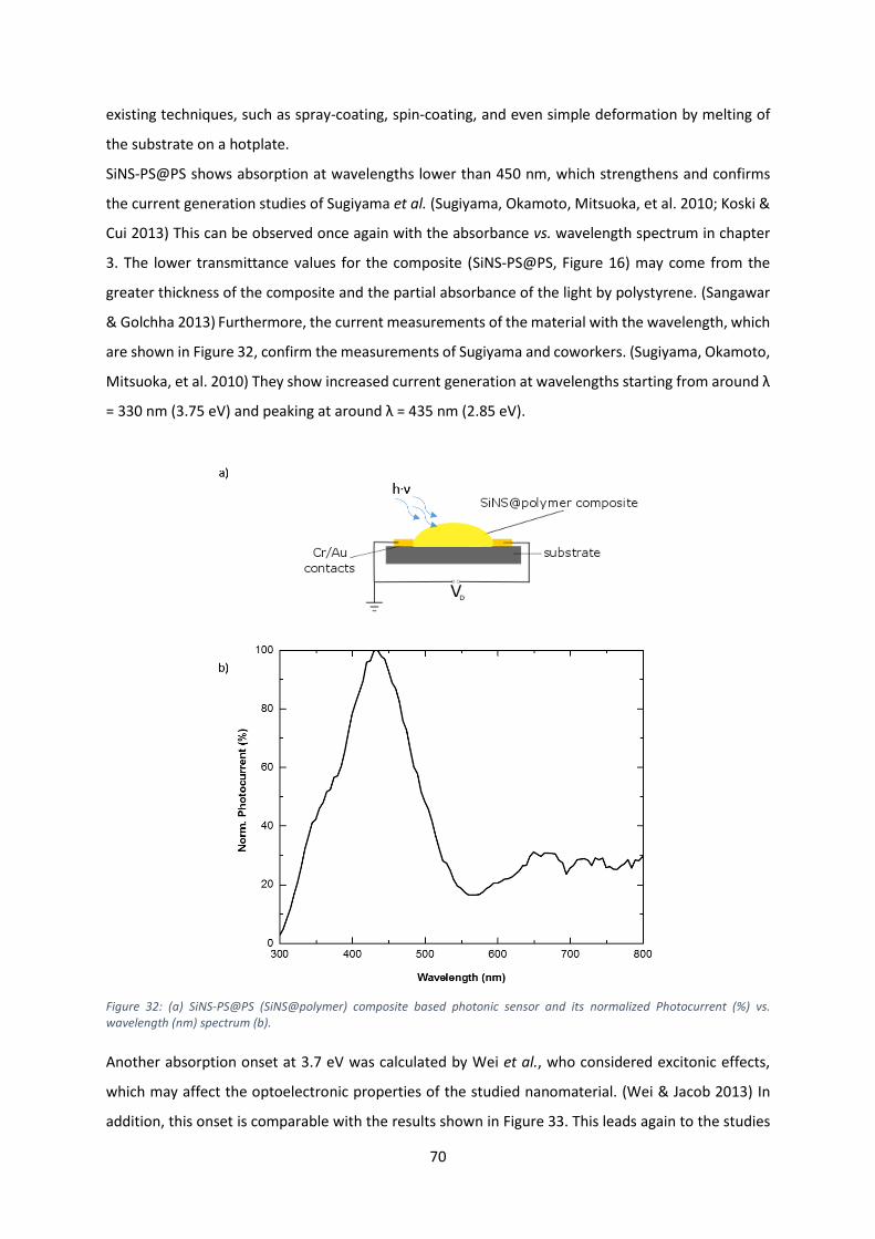
70
existing techniques, such as spray-coating, spin-coating, and even simple deformation by melting of
the substrate on a hotplate.
SiNS-PS@PS shows absorption at wavelengths lower than 450 nm, which strengthens and confirms
the current generation studies of Sugiyama et al. (Sugiyama, Okamoto, Mitsuoka, et al. 2010; Koski &
Cui 2013) This can be observed once again with the absorbance vs. wavelength spectrum in chapter
3. The lower transmittance values for the composite (SiNS-PS@PS, Figure 16) may come from the
greater thickness of the composite and the partial absorbance of the light by polystyrene. (Sangawar
& Golchha 2013) Furthermore, the current measurements of the material with the wavelength, which
are shown in Figure 32, confirm the measurements of Sugiyama and coworkers. (Sugiyama, Okamoto,
Mitsuoka, et al. 2010) They show increased current generation at wavelengths starting from around λ
= 330 nm (3.75 eV) and peaking at around λ = 435 nm (2.85 eV).
Figure 32: (a) SiNS-PS@PS (SiNS@polymer) composite based photonic sensor and its normalized Photocurrent (%) vs. wavelength (nm) spectrum (b).
Another absorption onset at 3.7 eV was calculated by Wei et al., who considered excitonic effects,
which may affect the optoelectronic properties of the studied nanomaterial. (Wei & Jacob 2013) In
addition, this onset is comparable with the results shown in Figure 33. This leads again to the studies
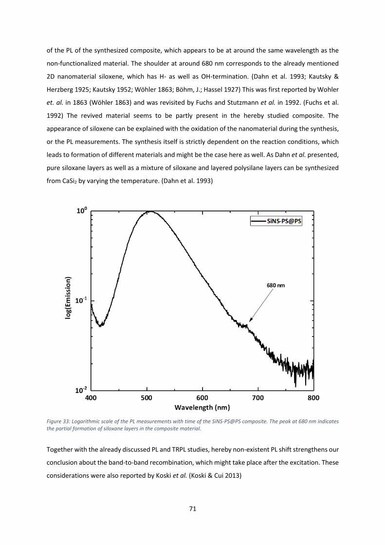
71
of the PL of the synthesized composite, which appears to be at around the same wavelength as the
non-functionalized material. The shoulder at around 680 nm corresponds to the already mentioned
2D nanomaterial siloxene, which has H- as well as OH-termination. (Dahn et al. 1993; Kautsky &
Herzberg 1925; Kautsky 1952; Wöhler 1863; Böhm, J.; Hassel 1927) This was first reported by Wohler
et. al. in 1863 (Wöhler 1863) and was revisited by Fuchs and Stutzmann et al. in 1992. (Fuchs et al.
1992) The revived material seems to be partly present in the hereby studied composite. The
appearance of siloxene can be explained with the oxidation of the nanomaterial during the synthesis,
or the PL measurements. The synthesis itself is strictly dependent on the reaction conditions, which
leads to formation of different materials and might be the case here as well. As Dahn et al. presented,
pure siloxane layers as well as a mixture of siloxane and layered polysilane layers can be synthesized
from CaSi2 by varying the temperature. (Dahn et al. 1993)
Figure 33: Logarithmic scale of the PL measurements with time of the SiNS-PS@PS composite. The peak at 680 nm indicates the partial formation of siloxane layers in the composite material.
Together with the already discussed PL and TRPL studies, hereby non-existent PL shift strengthens our
conclusion about the band-to-band recombination, which might take place after the excitation. These
considerations were also reported by Koski et al. (Koski & Cui 2013)
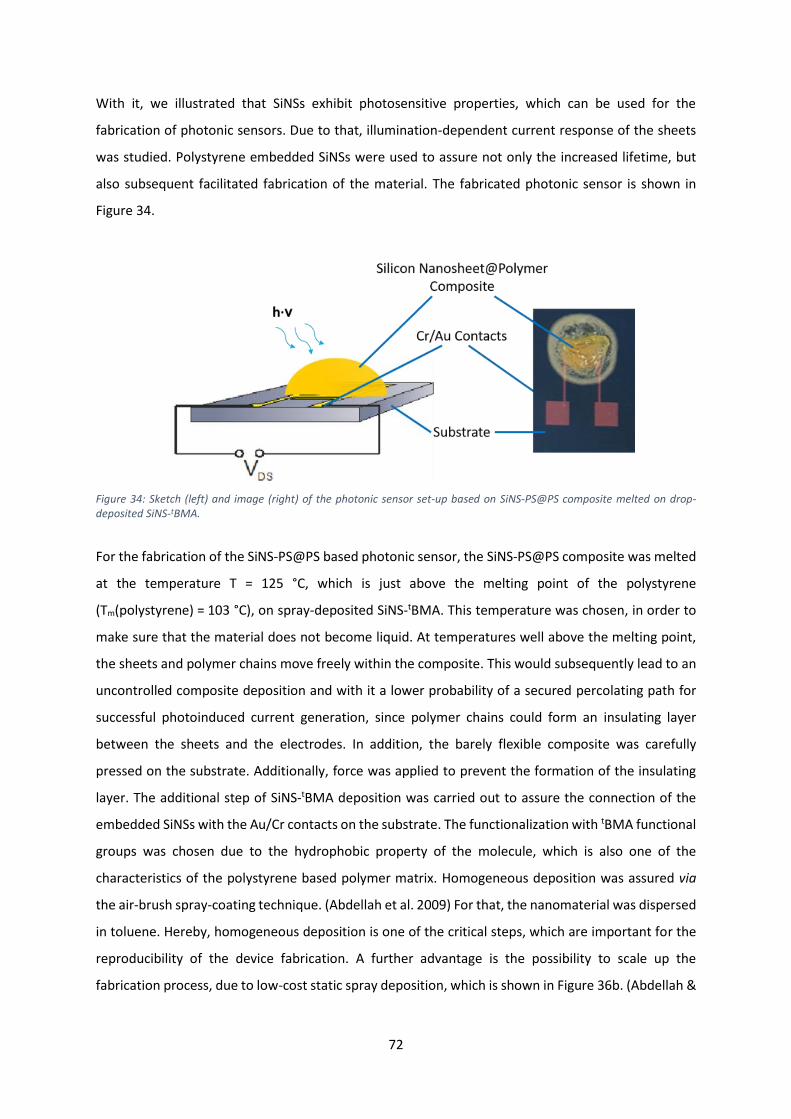
72
With it, we illustrated that SiNSs exhibit photosensitive properties, which can be used for the
fabrication of photonic sensors. Due to that, illumination-dependent current response of the sheets
was studied. Polystyrene embedded SiNSs were used to assure not only the increased lifetime, but
also subsequent facilitated fabrication of the material. The fabricated photonic sensor is shown in
Figure 34.
Figure 34: Sketch (left) and image (right) of the photonic sensor set-up based on SiNS-PS@PS composite melted on drop-deposited SiNS-tBMA.
For the fabrication of the SiNS-PS@PS based photonic sensor, the SiNS-PS@PS composite was melted
at the temperature T = 125 °C, which is just above the melting point of the polystyrene
(Tm(polystyrene) = 103 °C), on spray-deposited SiNS-tBMA. This temperature was chosen, in order to
make sure that the material does not become liquid. At temperatures well above the melting point,
the sheets and polymer chains move freely within the composite. This would subsequently lead to an
uncontrolled composite deposition and with it a lower probability of a secured percolating path for
successful photoinduced current generation, since polymer chains could form an insulating layer
between the sheets and the electrodes. In addition, the barely flexible composite was carefully
pressed on the substrate. Additionally, force was applied to prevent the formation of the insulating
layer. The additional step of SiNS-tBMA deposition was carried out to assure the connection of the
embedded SiNSs with the Au/Cr contacts on the substrate. The functionalization with tBMA functional
groups was chosen due to the hydrophobic property of the molecule, which is also one of the
characteristics of the polystyrene based polymer matrix. Homogeneous deposition was assured via
the air-brush spray-coating technique. (Abdellah et al. 2009) For that, the nanomaterial was dispersed
in toluene. Hereby, homogeneous deposition is one of the critical steps, which are important for the
reproducibility of the device fabrication. A further advantage is the possibility to scale up the
fabrication process, due to low-cost static spray deposition, which is shown in Figure 36b. (Abdellah &
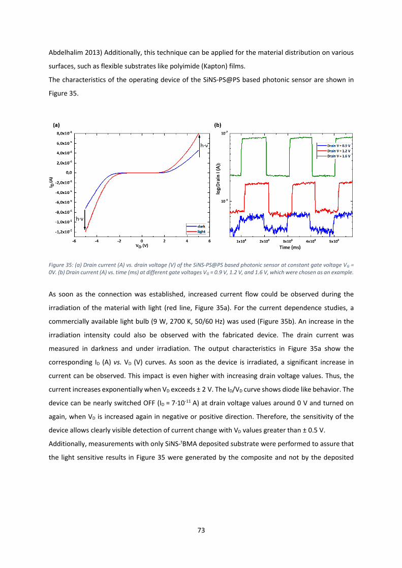
73
Abdelhalim 2013) Additionally, this technique can be applied for the material distribution on various
surfaces, such as flexible substrates like polyimide (Kapton) films.
The characteristics of the operating device of the SiNS-PS@PS based photonic sensor are shown in
Figure 35.
Figure 35: (a) Drain current (A) vs. drain voltage (V) of the SiNS-PS@PS based photonic sensor at constant gate voltage VG = 0V. (b) Drain current (A) vs. time (ms) at different gate voltages VG = 0.9 V, 1.2 V, and 1.6 V, which were chosen as an example.
As soon as the connection was established, increased current flow could be observed during the
irradiation of the material with light (red line, Figure 35a). For the current dependence studies, a
commercially available light bulb (9 W, 2700 K, 50/60 Hz) was used (Figure 35b). An increase in the
irradiation intensity could also be observed with the fabricated device. The drain current was
measured in darkness and under irradiation. The output characteristics in Figure 35a show the
corresponding ID (A) vs. VD (V) curves. As soon as the device is irradiated, a significant increase in
current can be observed. This impact is even higher with increasing drain voltage values. Thus, the
current increases exponentially when VD exceeds ± 2 V. The ID/VD curve shows diode like behavior. The
device can be nearly switched OFF (ID = 7∙10-11 A) at drain voltage values around 0 V and turned on
again, when VD is increased again in negative or positive direction. Therefore, the sensitivity of the
device allows clearly visible detection of current change with VD values greater than ± 0.5 V.
Additionally, measurements with only SiNS-tBMA deposited substrate were performed to assure that
the light sensitive results in Figure 35 were generated by the composite and not by the deposited
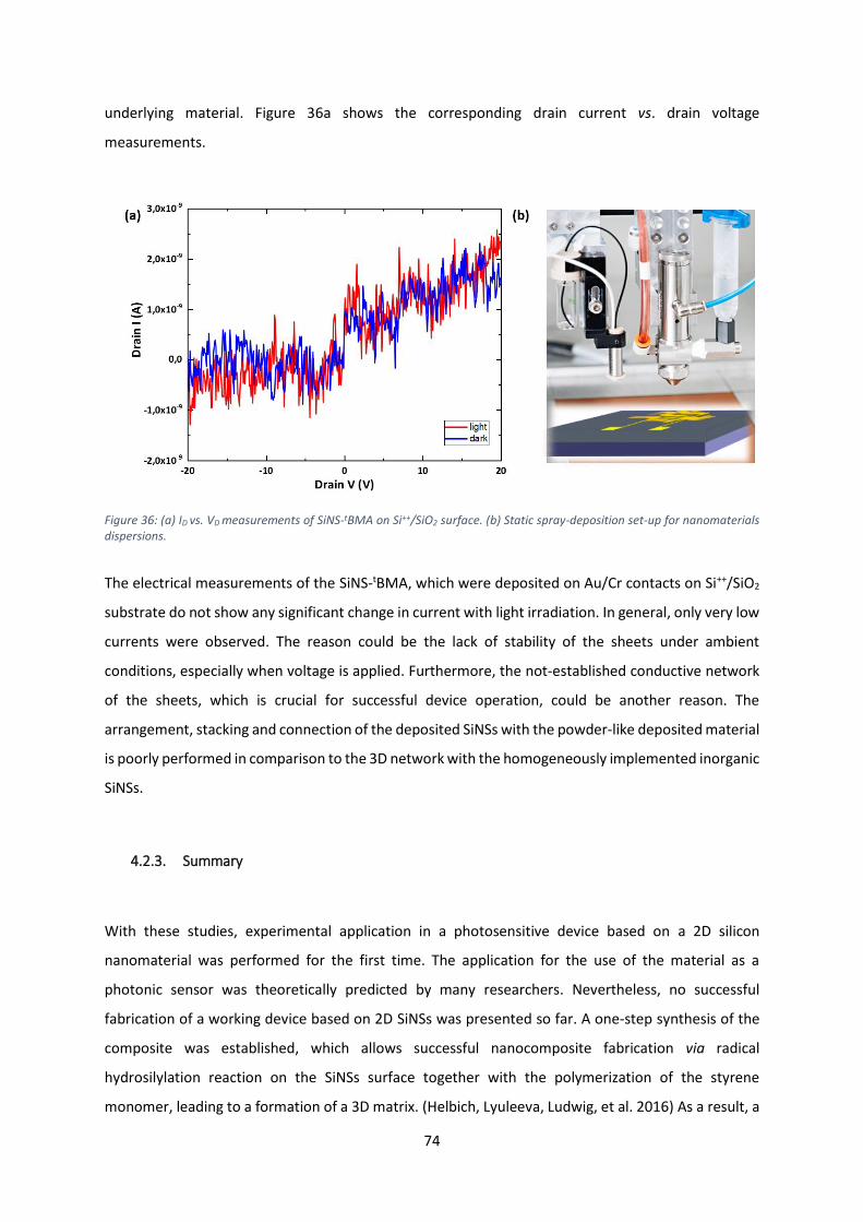
74
underlying material. Figure 36a shows the corresponding drain current vs. drain voltage
measurements.
Figure 36: (a) ID vs. VD measurements of SiNS-tBMA on Si++/SiO2 surface. (b) Static spray-deposition set-up for nanomaterials dispersions.
The electrical measurements of the SiNS-tBMA, which were deposited on Au/Cr contacts on Si++/SiO2
substrate do not show any significant change in current with light irradiation. In general, only very low
currents were observed. The reason could be the lack of stability of the sheets under ambient
conditions, especially when voltage is applied. Furthermore, the not-established conductive network
of the sheets, which is crucial for successful device operation, could be another reason. The
arrangement, stacking and connection of the deposited SiNSs with the powder-like deposited material
is poorly performed in comparison to the 3D network with the homogeneously implemented inorganic
SiNSs.
4.2.3. Summary
With these studies, experimental application in a photosensitive device based on a 2D silicon
nanomaterial was performed for the first time. The application for the use of the material as a
photonic sensor was theoretically predicted by many researchers. Nevertheless, no successful
fabrication of a working device based on 2D SiNSs was presented so far. A one-step synthesis of the
composite was established, which allows successful nanocomposite fabrication via radical
hydrosilylation reaction on the SiNSs surface together with the polymerization of the styrene
monomer, leading to a formation of a 3D matrix. (Helbich, Lyuleeva, Ludwig, et al. 2016) As a result, a

75
multifunctional composite was synthesized, which possesses both materials properties, allowing its
deformation with increased temperatures and showing light dependent conductivity.
These studies lay the foundation for further fabrication approaches of sensing 2D nanosilicon-based
devices. Additionally, the theoretical studies, which predicted outstanding properties of the layered
polysilane, are herewith reinforced and their already remarkable value of sensitivity and conductivity
increased.
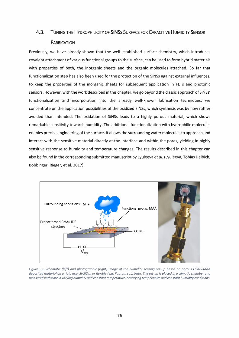
76
4.3. TUNING THE HYDROPHILICITY OF SINSS SURFACE FOR CAPACITIVE HUMIDITY SENSOR
FABRICATION
Previously, we have already shown that the well-established surface chemistry, which introduces
covalent attachment of various functional groups to the surface, can be used to form hybrid materials
with properties of both, the inorganic sheets and the organic molecules attached. So far that
functionalization step has also been used for the protection of the SiNSs against external influences,
to keep the properties of the inorganic sheets for subsequent application in FETs and photonic
sensors. However, with the work described in this chapter, we go beyond the classic approach of SiNSs’
functionalization and incorporation into the already well-known fabrication techniques: we
concentrate on the application possibilities of the oxidized SiNSs, which synthesis was by now rather
avoided than intended. The oxidation of SiNSs leads to a highly porous material, which shows
remarkable sensitivity towards humidity. The additional functionalization with hydrophilic molecules
enables precise engineering of the surface. It allows the surrounding water molecules to approach and
interact with the sensitive material directly at the interface and within the pores, yielding in highly
sensitive response to humidity and temperature changes. The results described in this chapter can
also be found in the corresponding submitted manuscript by Lyuleeva et al. (Lyuleeva, Tobias Helbich,
Bobbinger, Rieger, et al. 2017)
Figure 37: Schematic (left) and photographic (right) image of the humidity sensing set-up based on porous OSiNS-MAA deposited material on a rigid (e.g. Si/SiO2), or flexible (e.g. Kapton) substrate. The set-up is placed in a climatic chamber and measured with time in varying humidity and constant temperature, or varying temperature and constant humidity conditions.
77
4.3.1. State of the Art and Aim
Water is one of the most common molecules in the environment. Its ratio in atmosphere has a
significant impact on our everyday-life and therefore needs to be controlled, in order to prevent
unexpected results especially in industrial processing. (Traversa 1995) The manufacturer needs to rely
on the reproducibility of the product, just as the customer relies on the quality, stability and durability
of the purchased device. This reproducibility can be harmed by the amount of water vapor present
during the device fabrication in e.g., semiconductor industry. The food industry relies on the shelf life
of the product, which can only be guaranteed if the absence of water is assured. (Mathlouthi 2001)
That value may be monitored and strictly traced by humidity sensing devices. (Chen & Lu 2005) In
summary, water vapor control provokes a wide interest in materials science and electrical engineering.
Since the industry is constantly chasing after cheaper and smarter solutions, research must find new
ways to use the physics of not only natal materials, but also synthetically made ones. Furthermore,
experimental and fundamental research encompasses nanoscopic materials for the satisfaction of the
industrial needs. Once again, the class of 2D materials such as graphene (Novoselov et al. 2004), MoS2
(Mak et al. 2010), germanene and silicene (Chowdhury & Jana 2016) provide interesting possibilities
due to their already mentioned outstanding properties. Thus, for example, in direct-gap or indirect-
gap semiconductors (Yamanaka et al. 1996; Bianco et al. 2013; Jiang et al. 2014; Xu et al. 2013;
Dettlaff-Weglikowska et al. 1997), conductivity, or semiconductivity (Matthes et al. 2014) and further
features, coming with for example quantum confinement (Wilcoxon et al. 1999), while lowering the
size of the material, spark interest. Two important aspects for an innovative electronics industry,
which arises with smaller size and dimensionality, are transparency and flexibility of the considered
materials. On one hand it allows the fabrication of invisible electronics, which is desired from an
esthetical prospective and provides water level control without distracting the perception of the
average customer. On the other hand, it makes the fabrication of highly flexible and even stretchable
devices for atmospheric conditions possible, which is required for the comfort factor of the wearables,
manufactured from these low-dimensionality materials.
For the humidity control, the amount of water in gas needs to be determined. (Roger et al. 2016) The
ratio of the partial pressure of water in gas to the saturation vapor pressure of a gas at a given
temperature (Chen & Lu 2005), is one of the most commonly used values for high humidity ranges and
is referred to as relative humidity (RH). The following materials were reported to be suitable for
humidity sensitive measurements: ceramics, such as Al2O3 (Chakraborty et al. 1999), TiO2 (Morimoto
et al. 1969; McCafferty & Zettlemoyer 1971), SiO2 (Lin et al. 1993; D’apuzzo et al. 2000; Kong et al.
1997), spinel compounds, modified polyelectrolytes (Rauen et al. 1993; Sakai et al. 1996; M. S. Gong

78
et al. 2002; M.-S. Gong et al. 2002; Lee et al. 2013) and conductive polymers. (Macdiarmid 1987)
However, also 2D materials were used in recording ambient humidity. In the 2D world, graphene is a
trendsetter for the application of novel 2D structures and proved to be useful in form of graphene
oxide films. Its capacitance can be influenced by the surrounding water molecules, which was shown
by Borini et al. with their graphene oxide thin films. These were used for low cost transparent and
flexible sensor fabrication with response accuracies of up to 90%. (Borini et al. 2013)
Nevertheless, coming back to the mainly silicon-based sensors and electronics industry (Schulz 1999),
SiNSs have become very useful. The previously described goal in this work was focused on
encapsulation and protection of freestanding SiNSs (Helbich, Lyuleeva, Höhlein, et al. 2016; Helbich,
Lyuleeva, Ludwig, et al. 2016; T. Helbich et al. 2017) for semiconducting device fabrication purposes.
(Lyuleeva, Tobias Helbich, Rieger & Lugli 2017; Tobias Helbich et al. 2017; Lyuleeva, Philipp Holzmüller,
Helbich, Stutzmann, et al. 2017) Covalent hydrosilylation reactions for hybrid materials and
composites were carried out to embed the sheets chemically in a layer, or matrix of organic molecules.
However, for the detection of humidity and with it the fabrication of a capacitive humidity sensor,
dielectricity is desired over conductivity. The dielectric constant of the material can easily be tuned by
ad- or chemisorption of molecules on the surface. For that, the values of the dielectric constants of
the active layer and the approaching molecules, which need to be detected, need to be different. This
is true for the interaction of oxidized silicon (with a fairly low dielectric constant) and the surrounding
water molecules (which have a high dielectric constant). (Y. Wang et al. 2010) This effect may vary
with the value of relative permittivity, which can be used for detection purposes.
Additionally, as the example of porous silicon (p-Si) shows, high surface to volume ratio can be a good
basis for the fabrication of capacitive humidity sensors. (Y. Wang et al. 2010) The porosity is an
important aspect for a fast detection. (Sun et al. 1995) The interface physics and with it the interaction
of the molecules with the sensitive material plays a crucial role not only for the sensitivity of the
device, but also or the recovery of the material resulting in a fast response which is useful for sensor
applications. With facile adsorption-chemisorption and capillary processes of water at an interface,
fast humidity change response can be guaranteed. (Adamson & Gast 1997) All these factors can be
ensured with the use of oxidized silicon nanosheets (OSiNSs), which were fabricated for nanomaterial
based humidity sensing purposes. As already mentioned in chapter 1.2., 2D silicon has a very high
surface-to-volume ratio, since (owing to its low dimensionality) this material consists of only surface
molecules. (Helbich, Lyuleeva, Ludwig, et al. 2016) This property also leads to the agglomeration of
the sheets, which was prevented so far with chemical modification of the surface and subsequent
dispersion in different solvents. These stable dispersions can then be used in subsequent fabrication
steps. However, this property to easily agglomerate is beneficial for this case, since the agglomeration
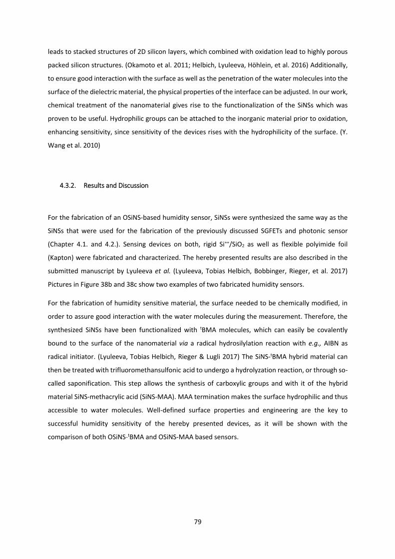
79
leads to stacked structures of 2D silicon layers, which combined with oxidation lead to highly porous
packed silicon structures. (Okamoto et al. 2011; Helbich, Lyuleeva, Höhlein, et al. 2016) Additionally,
to ensure good interaction with the surface as well as the penetration of the water molecules into the
surface of the dielectric material, the physical properties of the interface can be adjusted. In our work,
chemical treatment of the nanomaterial gives rise to the functionalization of the SiNSs which was
proven to be useful. Hydrophilic groups can be attached to the inorganic material prior to oxidation,
enhancing sensitivity, since sensitivity of the devices rises with the hydrophilicity of the surface. (Y.
Wang et al. 2010)
4.3.2. Results and Discussion
For the fabrication of an OSiNS-based humidity sensor, SiNSs were synthesized the same way as the
SiNSs that were used for the fabrication of the previously discussed SGFETs and photonic sensor
(Chapter 4.1. and 4.2.). Sensing devices on both, rigid Si++/SiO2 as well as flexible polyimide foil
(Kapton) were fabricated and characterized. The hereby presented results are also described in the
submitted manuscript by Lyuleeva et al. (Lyuleeva, Tobias Helbich, Bobbinger, Rieger, et al. 2017)
Pictures in Figure 38b and 38c show two examples of two fabricated humidity sensors.
For the fabrication of humidity sensitive material, the surface needed to be chemically modified, in
order to assure good interaction with the water molecules during the measurement. Therefore, the
synthesized SiNSs have been functionalized with tBMA molecules, which can easily be covalently
bound to the surface of the nanomaterial via a radical hydrosilylation reaction with e.g., AIBN as
radical initiator. (Lyuleeva, Tobias Helbich, Rieger & Lugli 2017) The SiNS-tBMA hybrid material can
then be treated with trifluoromethansulfonic acid to undergo a hydrolyzation reaction, or through so-
called saponification. This step allows the synthesis of carboxylic groups and with it of the hybrid
material SiNS-methacrylic acid (SiNS-MAA). MAA termination makes the surface hydrophilic and thus
accessible to water molecules. Well-defined surface properties and engineering are the key to
successful humidity sensitivity of the hereby presented devices, as it will be shown with the
comparison of both OSiNS-tBMA and OSiNS-MAA based sensors.
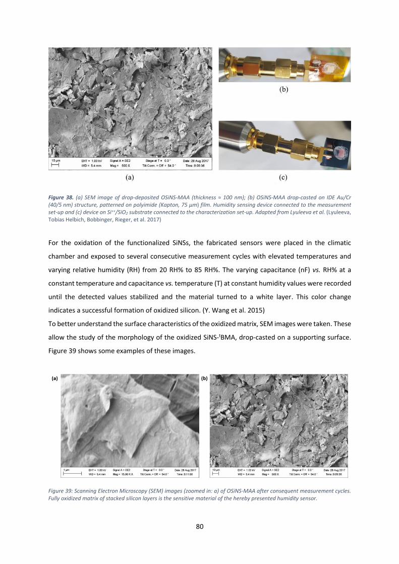
80
Figure 38. (a) SEM image of drop-deposited OSiNS-MAA (thickness ≈ 100 nm); (b) OSiNS-MAA drop-casted on IDE Au/Cr (40/5 nm) structure, patterned on polyimide (Kapton, 75 µm) film. Humidity sensing device connected to the measurement set-up and (c) device on Si++/SiO2 substrate connected to the characterization set-up. Adapted from Lyuleeva et al. (Lyuleeva, Tobias Helbich, Bobbinger, Rieger, et al. 2017)
For the oxidation of the functionalized SiNSs, the fabricated sensors were placed in the climatic
chamber and exposed to several consecutive measurement cycles with elevated temperatures and
varying relative humidity (RH) from 20 RH% to 85 RH%. The varying capacitance (nF) vs. RH% at a
constant temperature and capacitance vs. temperature (T) at constant humidity values were recorded
until the detected values stabilized and the material turned to a white layer. This color change
indicates a successful formation of oxidized silicon. (Y. Wang et al. 2015)
To better understand the surface characteristics of the oxidized matrix, SEM images were taken. These
allow the study of the morphology of the oxidized SiNS-tBMA, drop-casted on a supporting surface.
Figure 39 shows some examples of these images.
Figure 39: Scanning Electron Microscopy (SEM) images (zoomed in: a) of OSiNS-MAA after consequent measurement cycles. Fully oxidized matrix of stacked silicon layers is the sensitive material of the hereby presented humidity sensor.
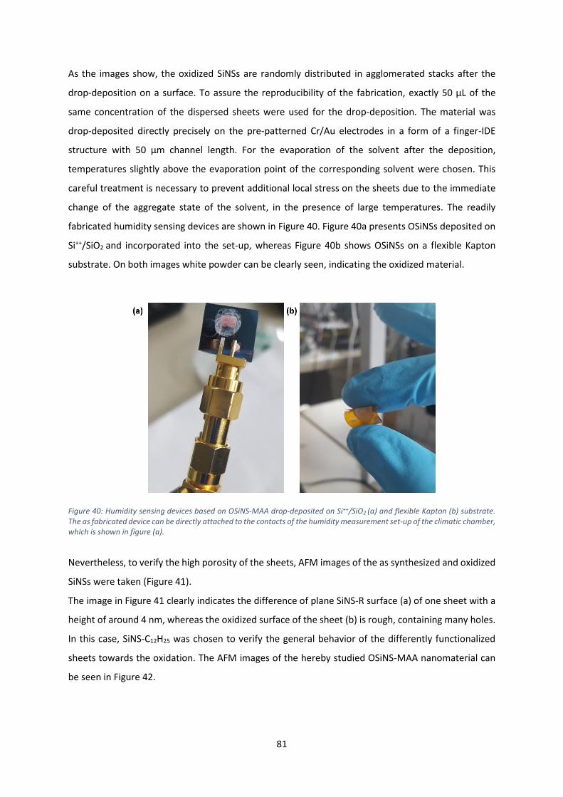
81
As the images show, the oxidized SiNSs are randomly distributed in agglomerated stacks after the
drop-deposition on a surface. To assure the reproducibility of the fabrication, exactly 50 μL of the
same concentration of the dispersed sheets were used for the drop-deposition. The material was
drop-deposited directly precisely on the pre-patterned Cr/Au electrodes in a form of a finger-IDE
structure with 50 μm channel length. For the evaporation of the solvent after the deposition,
temperatures slightly above the evaporation point of the corresponding solvent were chosen. This
careful treatment is necessary to prevent additional local stress on the sheets due to the immediate
change of the aggregate state of the solvent, in the presence of large temperatures. The readily
fabricated humidity sensing devices are shown in Figure 40. Figure 40a presents OSiNSs deposited on
Si++/SiO2 and incorporated into the set-up, whereas Figure 40b shows OSiNSs on a flexible Kapton
substrate. On both images white powder can be clearly seen, indicating the oxidized material.
Figure 40: Humidity sensing devices based on OSiNS-MAA drop-deposited on Si++/SiO2 (a) and flexible Kapton (b) substrate. The as fabricated device can be directly attached to the contacts of the humidity measurement set-up of the climatic chamber, which is shown in figure (a).
Nevertheless, to verify the high porosity of the sheets, AFM images of the as synthesized and oxidized
SiNSs were taken (Figure 41).
The image in Figure 41 clearly indicates the difference of plane SiNS-R surface (a) of one sheet with a
height of around 4 nm, whereas the oxidized surface of the sheet (b) is rough, containing many holes.
In this case, SiNS-C12H25 was chosen to verify the general behavior of the differently functionalized
sheets towards the oxidation. The AFM images of the hereby studied OSiNS-MAA nanomaterial can
be seen in Figure 42.
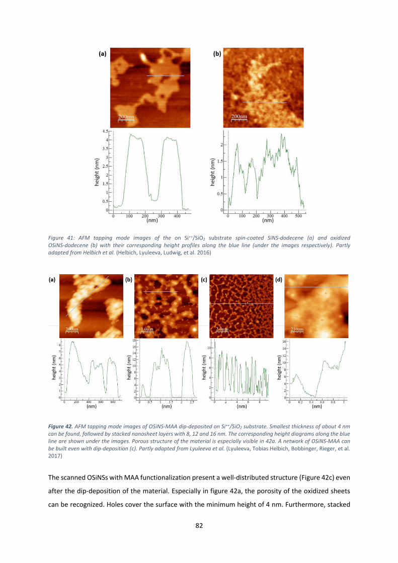
82
Figure 41: AFM tapping mode images of the on Si++/SiO2 substrate spin-coated SiNS-dodecene (a) and oxidized OSiNS-dodecene (b) with their corresponding height profiles along the blue line (under the images respectively). Partly adapted from Helbich et al. (Helbich, Lyuleeva, Ludwig, et al. 2016)
Figure 42. AFM tapping mode images of OSiNS-MAA dip-deposited on Si++/SiO2 substrate. Smallest thickness of about 4 nm can be found, followed by stacked nanosheet layers with 8, 12 and 16 nm. The corresponding height diagrams along the blue line are shown under the images. Porous structure of the material is especially visible in 42a. A network of OSiNS-MAA can be built even with dip-deposition (c). Partly adapted from Lyuleeva et al. (Lyuleeva, Tobias Helbich, Bobbinger, Rieger, et al. 2017)
The scanned OSiNSs with MAA functionalization present a well-distributed structure (Figure 42c) even
after the dip-deposition of the material. Especially in figure 42a, the porosity of the oxidized sheets
can be recognized. Holes cover the surface with the minimum height of 4 nm. Furthermore, stacked
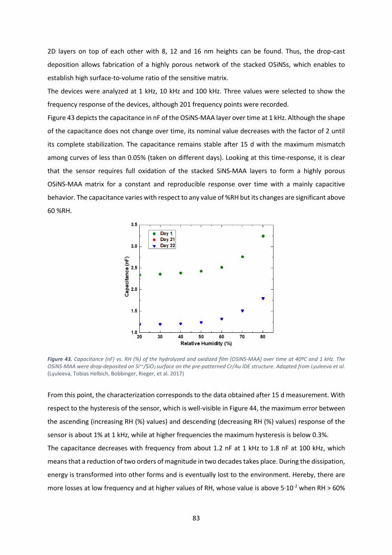
83
2D layers on top of each other with 8, 12 and 16 nm heights can be found. Thus, the drop-cast
deposition allows fabrication of a highly porous network of the stacked OSiNSs, which enables to
establish high surface-to-volume ratio of the sensitive matrix.
The devices were analyzed at 1 kHz, 10 kHz and 100 kHz. Three values were selected to show the
frequency response of the devices, although 201 frequency points were recorded.
Figure 43 depicts the capacitance in nF of the OSiNS-MAA layer over time at 1 kHz. Although the shape
of the capacitance does not change over time, its nominal value decreases with the factor of 2 until
its complete stabilization. The capacitance remains stable after 15 d with the maximum mismatch
among curves of less than 0.05% (taken on different days). Looking at this time-response, it is clear
that the sensor requires full oxidation of the stacked SiNS-MAA layers to form a highly porous
OSiNS-MAA matrix for a constant and reproducible response over time with a mainly capacitive
behavior. The capacitance varies with respect to any value of %RH but its changes are significant above
60 %RH.
Figure 43. Capacitance (nF) vs. RH (%) of the hydrolyzed and oxidized film (OSiNS-MAA) over time at 40ºC and 1 kHz. The OSiNS-MAA were drop-deposited on Si++/SiO2 surface on the pre-patterned Cr/Au IDE structure. Adapted from Lyuleeva et al. (Lyuleeva, Tobias Helbich, Bobbinger, Rieger, et al. 2017)
From this point, the characterization corresponds to the data obtained after 15 d measurement. With
respect to the hysteresis of the sensor, which is well-visible in Figure 44, the maximum error between
the ascending (increasing RH (%) values) and descending (decreasing RH (%) values) response of the
sensor is about 1% at 1 kHz, while at higher frequencies the maximum hysteresis is below 0.3%.
The capacitance decreases with frequency from about 1.2 nF at 1 kHz to 1.8 nF at 100 kHz, which
means that a reduction of two orders of magnitude in two decades takes place. During the dissipation,
energy is transformed into other forms and is eventually lost to the environment. Hereby, there are
more losses at low frequency and at higher values of RH, whose value is above 5·10-2 when RH > 60%
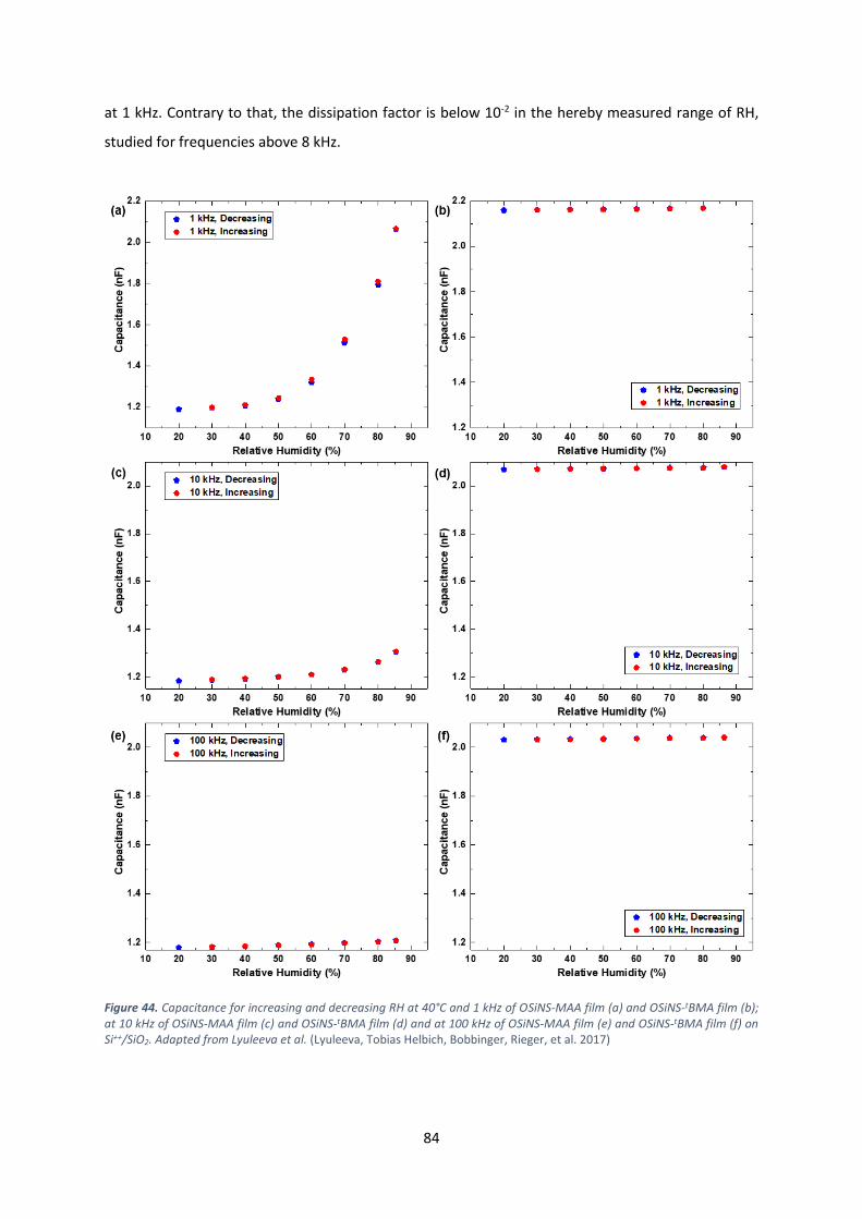
84
at 1 kHz. Contrary to that, the dissipation factor is below 10-2 in the hereby measured range of RH,
studied for frequencies above 8 kHz.
Figure 44. Capacitance for increasing and decreasing RH at 40°C and 1 kHz of OSiNS-MAA film (a) and OSiNS-tBMA film (b); at 10 kHz of OSiNS-MAA film (c) and OSiNS-tBMA film (d) and at 100 kHz of OSiNS-MAA film (e) and OSiNS-tBMA film (f) on Si++/SiO2. Adapted from Lyuleeva et al. (Lyuleeva, Tobias Helbich, Bobbinger, Rieger, et al. 2017)
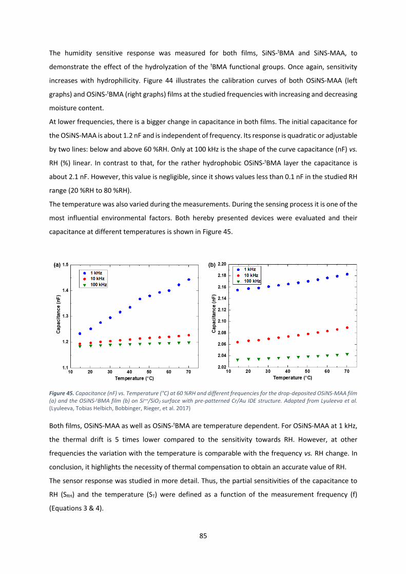
85
The humidity sensitive response was measured for both films, SiNS-tBMA and SiNS-MAA, to
demonstrate the effect of the hydrolyzation of the tBMA functional groups. Once again, sensitivity
increases with hydrophilicity. Figure 44 illustrates the calibration curves of both OSiNS-MAA (left
graphs) and OSiNS-tBMA (right graphs) films at the studied frequencies with increasing and decreasing
moisture content.
At lower frequencies, there is a bigger change in capacitance in both films. The initial capacitance for
the OSiNS-MAA is about 1.2 nF and is independent of frequency. Its response is quadratic or adjustable
by two lines: below and above 60 %RH. Only at 100 kHz is the shape of the curve capacitance (nF) vs.
RH (%) linear. In contrast to that, for the rather hydrophobic OSiNS-tBMA layer the capacitance is
about 2.1 nF. However, this value is negligible, since it shows values less than 0.1 nF in the studied RH
range (20 %RH to 80 %RH).
The temperature was also varied during the measurements. During the sensing process it is one of the
most influential environmental factors. Both hereby presented devices were evaluated and their
capacitance at different temperatures is shown in Figure 45.
Figure 45. Capacitance (nF) vs. Temperature (°C) at 60 %RH and different frequencies for the drop-deposited OSiNS-MAA film (a) and the OSiNS-tBMA film (b) on Si++/SiO2 surface with pre-patterned Cr/Au IDE structure. Adapted from Lyuleeva et al. (Lyuleeva, Tobias Helbich, Bobbinger, Rieger, et al. 2017)
Both films, OSiNS-MAA as well as OSiNS-tBMA are temperature dependent. For OSiNS-MAA at 1 kHz,
the thermal drift is 5 times lower compared to the sensitivity towards RH. However, at other
frequencies the variation with the temperature is comparable with the frequency vs. RH change. In
conclusion, it highlights the necessity of thermal compensation to obtain an accurate value of RH.
The sensor response was studied in more detail. Thus, the partial sensitivities of the capacitance to
RH (SRH) and the temperature (ST) were defined as a function of the measurement frequency (f)
(Equations 3 & 4).
86
𝑆𝑅𝐻(𝑓) ≡ 𝜕𝐶𝑇=𝑐𝑡𝑒 (𝑅𝐻)
𝜕 𝑅𝐻 (3)
𝑆𝑇(𝑓) ≡ 𝜕𝐶RH=𝑐𝑡𝑒 (𝑇)
𝜕 𝑇 (4)
All measurements show that the coefficient of correlation is higher than 0.98, indicating a good
linearity (Table 4). Sensitivity of the OSiNS-tBMA film towards RH is higher at 100 kHz, which is contrast
to the OSiNS-MAA film response. In the case of the thermal sensitivity, both devices show the same
trend over frequency.
Table 4: Summary of sensitivities to RH and temperature for both characterized drop-deposited and oxidized films: OSiNS-MAA and OSiNS-tBMA
Frequency (kHz) OSiNS-MAA film OSiNS-tBMA film
S RH
(pF/
%R
H)
1 1.60 for RH< 60%
28.40 for RH< 60%
0.10
10 0.70 for RH< 60%
3.60 for RH< 60%
0.10
100 0.50 0.20
S T (p
F/ºC
) 1 3.80 0.50
10 0.60 0.40
100 0.30 0.20
The hydroxylation of the tBMA functional groups on the surface of the SiNSs as a tool to gain
hydrophilicity, which is suitable for the goal sensitivity, can lead to a good response of the silicon-
based nanomaterial towards RH. The hereby studied MAA functionalized and oxidized SiNSs films
show a capacitance of 1.2 nF at 1 kHz in ambient conditions and a sensitivity of about 1.6 pF/%RH
below 60 %RH and 28.4 pF/%RH above this RH value. The response is not linear, but it exhibits good
reproducibility and small hysteresis (less than 0.2% in the whole RH range).
As expected, no change with RH could be detected with the rather hydrophobic OSiNS-tBMA layer. Its
response towards temperature is 5 times higher at 1 kHz than its variation with moisture content. By
comparing the response of common polymer humidity sensors with our device, one will realize that
these significant changes in capacitance are extremely high. In polymer based sensors the capacitance
increases by only a few units (Rivadeneyra et al. 2016; Trung et al. 2017). However, this thermal drift
87
can be easily compensated by adding a meandered metal line as resistive temperature sensor.
(Molina-Lopez et al. 2012; Kinkeldei et al. 2011)
Wang et al. demonstrated the characteristics of humidity sensing devices based on macroporous
silicon, which was modified with a metal oxide layer. (Y. Wang et al. 2010) This sensor has shown a
maximum hysteresis of 3.3 % at 200 kHz. Additionally, it presented good repeatability and long-term
stability. The capacitance of this sensor increased with RH increase with a behavior in frequency,
comparable with the hereby studied OSiNS-MAA films. Wang et al. demonstrated that substitution in
the porous space of air by adsorbed water molecules, which caused the variation in capacitance during
the exposure to RH. This process could also be found in the hereby studied system, explaining the
sensitivity of the highly porous layered OSiNS-MAA. With respect to the sensitivity, the sensor of Wang
et al. was twice as sensitive as our OSiNS-MAA based device. However, the OSiNS-MAA sensor is one
order of magnitude smaller than the sensor made by Wang et al. The importance of this finding is that
capacitance (and therefore sensitivity) is proportional to the area of a device. Thus, for an order of
magnitude reduction in size, one would expect an order of magnitude reduction in sensitivity, which
we are clearly showing isn't the case.
Finally, it is important to notice that the surface modification of our sensor can be further used for
subsequent (bio)molecules immobilization. These (bio)molecules could target the precise detection
of, for example, various surrounding substrates (Melzer et al. 2016; Caterino et al. 2015) or gas
molecules (Balasubramanian & Burghard 2005; Lim et al. 2010), depending on the functionality of the
attached enzyme, or molecular group respectively.
4.3.3. Summary
These results present an important surface modification technique as an approach, which can be
applied to achieve sensor array selectivity. The devices described in this work show how the
functionalization of SiNSs with hydrophilic functional groups can be used to improve the sensitivity of
OSiNSs based devices towards RH. These sensors and the hereby presented technique can be helpful
for novel technology, which is in search of cheap and reproducible methods, without sacrificing the
quality of the sensor systems. Furthermore, it enables manufacturing of devices that are sensitive to
specific molecules. The hereby presented work uses straightforward syntheses in materials’ chemistry,
which can be applied as a tool for new and promising fabrication solutions.
88
5. SUMMARY AND OUTLOOK
This dissertation presents cutting-edge research, combining Chemistry, Physics and Engineering,
which helps to improve and broaden the spectrum of novel approaches in nanotechnology. The results
presented in this work do not only build a fundamental bridge between the theoretical research and
the preparative studies, but also provide solid ground for a new mind-set for reaching the desired
goals in novel sensing and (opto)electronic technologies. The main goal is to provide guidance for
scientists who work in the currently vital area of 2D nanomaterials - especially on the interface
between the mentioned research fields - and with it help them benefit from the herein presented
results.
Freestanding 2D silicon was recently introduced to the nanomaterials community and became the
main material for our research. It is believed to exhibit not only new, but also outstanding
(opto)electronic properties. These properties were predicted and confirmed with a variety of
theoretical calculations, followed eventually by experimental confirmation.
In this work, chemical exfoliation was used for the synthesis of hydrogenated SiNSs, starting with the
deintercalation of calcium ions from the crystalline CaSi2 compound. As a result, slightly buckled free-
standing 2D silicon sheets ranging from hundreds of nanometers to micrometers in size were
obtained. These sheets have been used for further radical hydrosilylation steps to chemically
functionalize the surface of the nanomaterial. Being nearly planar, the small dimensions of SiNSs open
up new properties and possibilities. Some examples are the green PL at around 510 nm, whose exact
origin was studied with the help of TRPL and TIPL measurements. Understanding the origin of the band
gap, the ability to tune it with functional groups covalently attached to the surface and the application
of the semiconducting behavior of the SiNSs were the main subjects of this work.
To enable the use of these nanomaterials in ambient conditions and especially for facile and big scale
fabrication, they need to be stabilized. The 2D-sheets tend to agglomerate easily due to their high
surface-to-volume ratio. Furthermore, they can be destroyed by high energy light (UV light) and
reaction with oxygen. As a result, the formation of silicon oxide, or silicon dioxide takes place, forming
an insulator with a wide energy band gap. This makes SiNSs not suitable for electronic applications as
semiconductor material. The stabilization of SiNSs can be reached with the help of covalent surface
functionalization, which was carried out in close collaboration with the group of Prof. Rieger at the
chair of Macromolecular Chemistry (TU Munich). Organic groups such as dodecene, styrene or tert-
butyl methacrylate (tBMA) were successfully attached using diazonium salt initiators for the first, or
thermal/AIBN induced reactions for the last two examples. As the related work, described in the
89
dissertation of Dr. Helbich (TUM, Chair of Macromolecular Chemistry, 2017) presents, the lifetime of
these silicon monolayers can be increased dramatically. Additionally, their fabrication is facilitated
with different material deposition techniques, such as for example spray-deposition or spin-coating.
Furthermore, dispersed solutions can be used in the future for the fabrication of highly precise,
reproducible and ultra-low-cost conductive patterns via inkjet printing technique, which is currently
under further investigation in our group.
Physical strain on the SiNSs, the underlying substrate, external electrical fields and surface
functionalization are predicted to have an influence on the band gap of the 2D silicon. These external
influences may be able to manipulate the range of the band gap and need to be investigated in more
detail. They are believed to be useful for direct manipulation of the PL, leading to light emission of
different wavelengths.
The results presented herein, describe the attempt to shift the PL with the help of chemical surface
modification. Nevertheless, no promising results could be achieved so far. Interestingly, all these SiNSs
based composites, hybrid materials and bare freestanding sheets (SiNS-H) exhibit the consistent green
PL at around 510 nm. As already mentioned, this PL could neither be shifted with the various covalent
functionalizations on the surface, nor with the temperature. No one has studied and understood the
origin of this light emission of the SiNSs so far. Thus, for the first time time-resolved PL and time-
integrated PL studies have been carried out in combination with measurements at different
temperatures (from room temperature down to 5 K). As a result, our group could confirm that the PL
is band-like. Additionally, we observed a long exponential tail, also referred to as the Urbach tail, which
is due to the band-tail states. It arises from the ‘locked-in’ structural disorder in the sheets, present
due to the nature of the SiNSs after their chemical exfoliation. To liberate the sheets from their packed
structure in the crystalline CaSi2, harsh conditions, such as various solvents, ultra-sonication, freeze-
drying, chemical treatment with hydrochloric acid and hydrofluoric acid have been undertaken. Each
step causes damage to the 2D structure, which might result in additional disorder of the surface and
holes in the sheets. This disorder additionally ranges with the type of the molecules which were
covalently attached to the surface. This has exclusively an impact on the Urbach band-tail and could
be clearly observed with our measurements. Already these results do not only build a fundamental
bridge between the knowledge of the physics of the herein described material and the preparative
studies, but also provide solid ground for a so far not described behavior of the disorder dependent
band-tail states in 2D systems.
Based on the investigations described, new devices such as e.g., SiNSs based field-effect transistors,
photonic or humidity sensors can be fabricated. We showed that SiNSs-polymer based composites can
90
be formed via simultaneous radical functionalization of SiNSs and polymer matrix formation (polymer
= polystyrene, poly(acrylic acid)). As a result, a three-dimensional network is formed, which opens up
even more new possibilities for application due to the added features of the polymer. New
photosensitive devices can be built based on these composites. Especially in the case of polystyrene,
SiNS-PS@PS can be synthesized and melted on top of pre-patterned gold electrodes, forming an
optoelectronic sensor. Highly sensitive optical response can be detected using this device, while
exposing it to a light source with wavelengths under around 450 nm.
Another successful way to realize the SiNSs in the applied nanotechnology field was found to be the
improvement of the already well-known P3HT based solution-gated FETs. For the desired combination
with the up to now widely used organic semiconducting polymer P3HT, the surface of the SiNSs was
modified with various functional groups. The choice of these groups was concentrated on the precise
engineering of the nanomaterial’s surface, with the aim to establish best interaction with the polymer
chains. Thus, most homogeneous thin films could be fabricated for the desired SGFETs. At the same
time, its remarkable properties, such as the green PL, ambipolarity and semiconductivity were
preserved. Surface modification with thiophene acetylene functional molecules has proven to be the
best approach, due to the molecule’s chemical and physical similarity to the repeating units, which
are found within the P3HT. As a result, the herein mentioned combination of chemically modified
SiNSs with P3HT lead to the fabrication of an improved hybrid material based SGFET with ON currents
4 times higher than the ones of the solely P3HT based devices.
Up to now, protection of the SiNSs from external influences, such as oxygen and light for further
application as ambipolar semiconducting material was the main aim of the herein described research.
Nevertheless, with the next application we went beyond the classic approach of SiNSs’ synthesis,
functionalization and incorporation into the already well-known fabrication techniques: our group
concentrated on the application possibilities of the byproducts, namely the silicon (di)oxide, which
were by now rather avoided than intended. With the third application we demonstrate that the
oxidation of SiNSs leads to a highly porous material OSiNSs, which shows remarkable sensitivity
towards humidity. Additional functionalization with hydrophilic molecules enables precise
engineering of the surface. It allows the surrounding water molecules to approach and interact with
the sensitive material directly at the interface and also within the pores, yielding a highly sensitive
response to humidity and temperature changes. Herein, tBMA was used as the organic molecule for
modification of the surface. The tert-butylic ester group of the methacrylic acid, can be exposed to
hydroxylation. This reaction step leads to the formation of carboxylic groups on top of the surface and
thus results in a facile transformation of the properties of the hybrid material from hydrophobic to

91
hydrophilic. Due to the surrounding water molecules, which can now easily interact with the
hydrophilic hybrid material and influence its dielectric behavior, a change in the capacitance can be
detected. The material’s response to humidity (25 %RH to 95 %RH) and temperature were successfully
detected.
In conclusion, these results do not only build a fundamental bridge between theoretical research,
understanding of the basic physical and chemical behavior of the inorganic material and its fabrication
techniques, but also provide solid ground for a new mind-set for reaching the desired goals in
nanotechnology. This original work can be applied to further novel nanomaterials and facilitate their
treatment and subsequent application in novel devices. For example, SiNS can be combined with other
monolayered nanostructures such as phosphorene, germanene, graphene and further newly
synthesized 2D monolayers. The 2D research community is concentrating on the fabrication of self-
stacking heterostructures, relying on the basic physical forces such as van der Waals interactions
between the sheets. They promise to open new possibilities for application by widening the range of
the fundamental and so far unexplored properties.
92
6. REFERENCES
Abdellah, A. et al., 2009. Exploring spray technology for the fabrication of organic devices based on
poly(3-hexylthiophene). 2009 9th IEEE Conference on Nanotechnology (IEEE-NANO), 8, pp.831–
834.
Abdellah, A. & Abdelhalim, A., 2013. Flexible Carbon Nanotube Based Gas Sensors Fabricated by Large-
Scale Spray Deposition. IEEE Sensors Journal, 13(October), pp.4014–4021. Available at:
http://ieeexplore.ieee.org/iel7/7361/6583958/06527935.pdf?arnumber=6527935.
Adamson, A.W. & Gast, A.P., 1997. Physical Chemistry of Surfaces 6th ed., New York. Available at:
http://www.degruyter.com/doi/10.1524/zpch.1999.210.Part_1.134.
Al-Ibrahim, M. et al., 2005. The influence of the optoelectronic properties of poly(3-alkylthiophenes)
on the device parameters in flexible polymer solar cells. Organic Electronics: physics, materials,
applications, 6(2), pp.65–77.
Allen, B.L., Kichambare, P.D. & Star, A., 2007. Carbon nanotube field-effect-transistor-based
biosensors. Advanced Materials, 19(11), pp.1439–1451.
Anslyn, E. V. & Dougherty, D.A., 2005. Modern Physical Organic Chemistry. In Modern Physical Organic
Chemistry. University Science Books.
Apeloig, Y. et al., 2000. Polysilyl radicals: EPR study of the formation and decomposition of star
polysilanes. Applied Magnetic Resonance, 18(3), pp.425–434.
Arivalagan, K. et al., 2011. Nanomaterials and its potential applications. International Journal of
ChemTech Research, 3(2), pp.534–538.
Aswal, D.K. et al., 2006. Self assembled monolayers on silicon for molecular electronics. Analytica
Chimica Acta, 568(1–2), pp.84–108.
Aufray, B. et al., 2010. Graphene-like silicon nanoribbons on Ag(110): A possible formation of silicene.
Applied Physics Letters, 96(18), pp.1–4.
Balasubramanian, K. & Burghard, M., 2005. Chemically functionalized carbon nanotubes. Small, 1(2),
pp.180–192.
Balendhran, S. et al., 2015. Elemental analogues of graphene: Silicene, germanene, stanene, and
phosphorene. Small, 11(6).
Barkelid, M. & Zwiller, V., 2013. Photocurrent generation in semiconducting and metallic carbon
93
nanotubes. Nature Photonics, 8(January), pp.47–51. Available at:
http://dx.doi.org/10.1038/nphoton.2013.311%5Cnhttp://www.nature.com/doifinder/10.1038/
nphoton.2013.311.
Barreda, J.L. et al., 2017. Multiple Schottky Barrier-Limited Field-Effect Transistors on a Single Silicon
Nanowire with an Intrinsic Doping Gradient. ACS Applied Materials and Interfaces, 9(13),
pp.12046–12053.
Baum, M. & Brittain, W.J., 2002. Synthesis of Polymer Brushes on Silicate Substrates via Reversible
Addition Fragmentation Chain Transfer Technique. Society, pp.610–615.
Bekyarova, E. et al., 2009. Chemical Modification of Epitaxial Graphene:Spontaneous Grafting of Aryl
Groups. Journal of American Chemical Society, 131(2), pp.1336–1337.
Bianco, E. et al., 2013. Stability and Exfoliation of Germanane : A Germanium Graphane Analogue. ,
(5), pp.4414–4421.
Blanksby, S.J. & Ellison, G.B., 2003. Bond dissociation energies of organic molecules. Accounts of
Chemical Research, 36(4), pp.255–263.
Bo, X.Z. et al., 2005. Carbon nanotubes-semiconductor networks for organic electronics: The pickup
stick transistor. Applied Physics Letters, 86(18), pp.1–3.
Böhm, J.; Hassel, O., 1927. Die Kristallstruktur des Calciumsilicids CaSi,. Z. anorg. allg. Chem., 160,
p.152.
Borini, S. et al., 2013. Ultrafast Graphene Oxide Humidity Sensors. ACS Nano, 7(12), pp.11166–11173.
Brennan, M.D., Morishita, T. & Spencer, M.J.S., 2016. Tuning the band gap of silicene by
functionalisation with naphthyl and anthracyl groups. The Journal of Chemical Physics, 144(11),
p.114704. Available at:
http://scitation.aip.org/content/aip/journal/jcp/144/11/10.1063/1.4943880.
Brennan, M.D., Morishita, T. & Spencer, M.J.S., 2016. Tuning the band gap of silicene by
functionalisation with naphthyl and anthracyl groups. Journal of Chemical Physics, 144(11).
Available at: http://dx.doi.org/10.1063/1.4943880.
Brinkmann, M. & Rannou, P., 2007. Effect of molecular weight on the structure and morphology of
oriented thin films of regioregular poly(3-hexylthiophene) grown by directional epitaxial
solidification. Advanced Functional Materials, 17(1), pp.101–108.
Brumfiel, G., 2013. Sticky problem snares wonder material. Nature, 495, p.152.
94
Brus, L., 1994. Luminescence of Silicon Materials: Chains, Sheets, Nanocrystals, Nanowires,
Microcrystals, and Porous Silicon. The Journal of Physical Chemistry, 98(14), pp.3575–3581.
Buriak, J.M., 2002. Organometallic chemistry on silicon and germanium surfaces. Chemical Reviews,
102(5), pp.1271–1308.
Buscema, M. et al., 2015. Photocurrent generation with two-dimensional van der Waals
semiconductors. Chem. Soc. Rev., 44, pp.3691–3718. Available at:
http://xlink.rsc.org/?DOI=C5CS00106D.
Cahangirov, S. et al., 2013. Electronic structure of silicene on Ag(111): Strong hybridization effects.
Physical Review B, 88(3), p.35432.
Cahangirov, S. et al., 2009. Two- and one-dimensional honeycomb structures of silicon and
germanium. Physical Review Letters, 102(June), pp.1–4.
Canham, L.T., 1990. Silicon quantum wire array fabrication by electrochemical and chemical
dissolution of wafers. Applied Physics Letters, 57(10), pp.1046–1048.
Caterino, R. et al., 2015. Photocurrent generation in diamond electrodes modified with reaction
centers. ACS applied materials & interfaces, 7(15), pp.8099–107.
Ceuster, J. De et al., 2001. High-frequency (95 GHz) electron paramagnetic resonance study of the
photoinduced charge transfer in conjugated polymer-fullerene composites. Physical Review B,
64(19), p.195206. Available at: https://link.aps.org/doi/10.1103/PhysRevB.64.195206.
Chakraborty, S. et al., 1999. Moisture sensitive field effect transistors using
\mathrm{SiO_2/Si_3N_4/Al_2O_3} gate structure. Smart Materials and Structures, 8(2), pp.274–
277. Available at: http://iopscience.iop.org/0964-1726/8/2/014.
Chandiramouli, R. & Nagarajan, V., 2016. Adsorption studies of NH3 molecules on functionalized
germanene nanosheet - A DFT study. Chemical Physics Letters, 665, pp.22–30. Available at:
http://dx.doi.org/10.1016/j.cplett.2016.10.048.
Chen, W. et al., 2007. Surface Transfer p-Type Doping of Epitaxial Graphene Surface Transfer p-Type
Doping of Epitaxial Graphene. J. Am. Chem. Soc., 129(16), pp.10418–10422.
Chen, Z. & Lu, C., 2005. Humidity Sensors: A Review of Materials and Mechanisms. Sensor Letters, 3(4),
pp.274–295. Available at: http://www.ingentaselect.com/rpsv/cgi-
bin/cgi?ini=xref&body=linker&reqdoi=10.1166/sl.2005.045.
Chiappe, D. et al., 2012. Local electronic properties of corrugated silicene phases. Advanced Materials,
95
24(37), pp.5088–5093.
Chiappe, D. et al., 2014. Two-dimensional Si nanosheets with local hexagonal structure on a MoS 2
surface. Advanced Materials, 26(13), pp.2096–2101.
Chimene, D., Alge, D.L. & Gaharwar, A.K., 2015. Two-Dimensional Nanomaterials for Biomedical
Applications: Emerging Trends and Future Prospects. Advanced Materials, 27(45), pp.7261–
7284.
Chow, W.L. et al., 2017. High Mobility 2D Palladium Diselenide Field-Effect Transistors with Tunable
Ambipolar Characteristics. Advanced Materials, 29(21), pp.1–8.
Chowdhury, S. & Jana, D., 2016. A theoretical review on electronic, magnetic and optical properties of
silicene. Reports on Progress in Physics, 79(12), p.126501.
Chuang, C.M. et al., 2014. Through Band Alignment Engineering. Nat Mater., 13(8), pp.796–801.
D’apuzzo, M. et al., 2000. Sol-Gel Synthesis of Humidity-Sensitive P2O5-SiO2 Amorphous Films. Journal
of Sol-Gel Science and Technology, 17, pp.247–254.
Dahn, J.R. et al., 1993. Structure of siloxene and layered polysilane (Si6H6). Physical Review B, 48(24),
pp.17872–17877.
Dalgarno, A. & Kingston, A.E., 1959. Van der Waals Forces. Proc. Phys. Soc., 73, p.455.
Dasog, M. et al., 2013. Chemical insight into the origin of red and blue photoluminescence arising from
freestanding silicon nanocrystals. ACS Nano, 7(3), pp.2676–2685.
Dasog, M. et al., 2016. Silicon nanocrystals and silicon-polymer hybrids: Synthesis, surface
engineering, and applications. Angewandte Chemie - International Edition, 55(7), pp.2322–2339.
Dasog, M. et al., 2014. Size vs Surface: Tuning the Photoluminescence of Freestanding Silicon
Nanocrystals Across the Visible Spectrum via Surface Groups. ACS Nano, 8(9), pp.9636–9648.
Degoli, E. & Ossicini, S., 2000. The electronic and optical properties of Si/SiO2 superlattices: role of
confined and defect states. Surface Sc, 470, pp.32–42.
Delerue, C., Allan, G. & Lannoo, M., 1993. Theoretical aspects of the luminescence of porous silicon.
Physical Review B, 48(15), pp.11024–11036.
Delley, B. & Steigmeier, E.F., 1993. Quantum confinement in Si nanocrystals. Physical Review B, 47(3),
pp.1397–1400. Available at: http://link.aps.org/doi/10.1103/PhysRevB.47.1397.
Derr, J. et al., 2009. Quantum confinement regime in silicon nanocrystals. Physica E: Low-Dimensional
96
Systems and Nanostructures, 41(4), pp.668–670.
Dettlaff-Weglikowska, U. et al., 1997. Structure and optical properties of the planar silicon compounds
polysilane and Wohler siloxene. Physical Review B, 56(20), pp.13132–13140.
Dietmueller, R. et al., 2009. Light-induced charge transfer in hybrid composites of organic
semiconductors and silicon nanocrystals. Applied Physics Letters, 94(11).
Ding, Y. & Wang, Y., 2012. Electronic structures of silicene fluoride and hydride. Applied Physics Letters,
100(8), p.83102.
Du, Y. et al., 2014. Device perspective for black phosphorus field-effect transistors: Contact resistance,
ambipolar behavior, and scaling. ACS Nano, 8(10), pp.10035–10042.
Edmondson, S., Osborne, V.L. & Huck, W.T.S., 2004. Polymer brushes via surface-initiated
polymerizations. Chemical Society Reviews, 33(1), p.14. Available at:
http://xlink.rsc.org/?DOI=b210143m.
Elias, D.C. et al., 2009. Control of Graphene’s Properties by Reversible Hydrogenation: Evidence for
Graphane. Science, 323(January), pp.610–613.
Erickson, D. et al., 2008. Nanobiosensors: Optofluidic, electrical and mechanical approaches to
biomolecular detection at the nanoscale. Microfluidics and Nanofluidics, 4(1–2), pp.33–52.
Feng, B. et al., 2012. Evidence of silicene in honeycomb structures of silicon on Ag (111). Nano letters,
12(7), pp.3507–3511.
Fiori, G. et al., 2014. Electronics based on two-dimensional materials. Nature nanotechnology,
9(October), pp.768–779.
Fleurence, A. et al., 2012. Experimental evidence for epitaxial silicene on diboride thin films. Physical
Review Letters, 108(24), pp.1–5.
Fuchs, H.D. et al., 1992. Visible luminescence from porous silicon and siloxene. Physica Scripta, T45,
pp.309–313.
Gang, C., Peng-Fei, L. & Zi-Tao, L., 2013. Influence of strain and electric field on the properties of
silicane. Chinese Physics B, 22(4), p.46201. Available at: http://stacks.iop.org/1674-
1056/22/i=4/a=046201?key=crossref.3bacdff018b241cd7fd800c368c89f03.
Gao, N., Zheng, W.T. & Jiang, Q., 2012. Density functional theory calculations for two-dimensional
silicene with halogen functionalization. Physical Chemistry Chemical Physics, 14(1), p.257.
97
Available at: http://www.ncbi.nlm.nih.gov/pubmed/22083171.
Gatoo, M.A. et al., 2014. Physicochemical properties of nanomaterials: Implication in associated toxic
manifestations. BioMed Research International, p.498420.
Geim, A.K. & Novoselov, K.S., 2007. The rise of graphene. Nature materials, 6, pp.183–191.
Gong, M.-S., Joo, S.-W. & Choi, B.-K., 2002. Humidity-sensitive properties of a cross-linked
polyelectrolyte prepared from mutually reactive copolymers. Journal of Materials Chemistry,
12(4), pp.902–906. Available at: http://xlink.rsc.org/?DOI=b108647m.
Gong, M.S., Joo, S.W. & Choi, B.K., 2002. Humidity sensor using mutually reactive copolymers
containing quaternary ammonium salt and reactive function. Sensors and Actuators, B: Chemical,
86(1), pp.81–87.
Grazianetti, C., Cinquanta, E. & Molle, A., 2016. Two-dimensional silicon: the advent of silicene. 2D
Materials, 3(1), p.12001. Available at: http://www.scopus.com/inward/record.url?eid=2-s2.0-
84964452703&partnerID=tZOtx3y1.
Guo, Q. et al., 2016. Black phosphorus mid-infrared photodetectors with high gain. Nano Letters,
16(7), pp.4648–4655.
Guo, Z.-X. et al., 2013. Absence of Dirac Electrons in Silicene on Ag(111) Surfaces. Journal of the
Physical Society of Japan, 82(6), p.63714.
Guo, Z.X. et al., 2015. Structural evolution and optoelectronic applications of multilayer silicene.
Physical Review B - Condensed Matter and Materials Physics, 92(20), pp.1–13.
Guzmán-Verri, G.G. & Lew Yan Voon, L.C., 2011. Band structure of hydrogenated Si nanosheets and
nanotubes. Journal of physics. Condensed matter : an Institute of Physics journal, 23(14),
p.145502. Available at: http://www.ncbi.nlm.nih.gov/pubmed/21430307.
Guzmán-Verri, G.G. & Lew Yan Voon, L.C., 2007. Electronic structure of silicon-based nanostructures.
Physical Review B - Condensed Matter and Materials Physics, 76(7).
Handy, J., 2014. The Biggest Problem Facing Semiconductors. online. Available at:
https://www.forbes.com/sites/jimhandy/2014/04/30/the-biggest-problem-facing-
semiconductors/#53725cd35093.
Harun, N.I. et al., 2012. Resistive-type Humidity Sensor Based on CA-NH4BF4-PEG600 Thin Films.
Physics Procedia, 25, pp.221–226. Available at:
http://linkinghub.elsevier.com/retrieve/pii/S1875389212004919.
98
Helbich, T. et al., 2017. Diaryliodonium salts as hydrosilylation initiators for the surface
functionalization of silicon nanomaterials and their collaborative effect as ring opening
polymerization initiators. Nanoscale, 9(23).
Helbich, T. et al., 2017. Lewis Acid Induced Functionalization of Photoluminescent Two-Dimensional
Silicon Nanosheets for the Fabrication of Functional Hybrid Films. Advanced Functional
Materials, p.1606764.
Helbich, T., Lyuleeva, A., Ludwig, T., et al., 2016. One-Step Synthesis of Photoluminescent Covalent
Polymeric Nanocomposites from 2D Silicon Nanosheets. Advanced Functional Materials, 26(37),
pp.6711–6718.
Helbich, T., Lyuleeva, A., Höhlein, I.M.D., et al., 2016. Radical-Induced Hydrosilylation Reactions for
the Functionalization of Two-Dimensional Hydride Terminated Silicon Nanosheets. Chemistry - A
European Journal, 22(18), pp.6194–6198.
Hengge, E. & Grupe, H., 1964. Bestimmung der Substituentenorientierung am Siloxen durch
Brückenbildung. Farbe und Fluoreszenz ringformiger Si-Verbindungen, 4, pp.1783–1788.
Hess, L.H. et al., 2011. Graphene transistor arrays for recording action potentials from electrogenic
cells. Advanced materials, 23, pp.5045–9. Available at:
http://www.ncbi.nlm.nih.gov/pubmed/21953832 [Accessed November 14, 2014].
Hess, L.H. et al., 2014. Graphene Transistors with Multifunctional Polymer Brushes for Biosensing
Applications. ACS Appl. Mater. Interfaces, 6, pp.9705–9710.
Hoffmann, R.W., 2004. Stereoselective synthesis using diastereotopic groups. Synthesis, (13),
pp.2075–2090.
Houssa, M. et al., 2011. Electronic properties of hydrogenated silicene and germanene. Applied Physics
Letters, 98(22), pp.96–99.
Hu, M. et al., 2001. Structure and morphology of self-assembled layers on silicon oxide. Applied
Surface Science, 181, pp.307–316. Available at:
http://www.sciencedirect.com/science/article/pii/S0169433201003993.
Hu, P. et al., 2013. Highly responsive ultrathin GaS nanosheet photodetectors on rigid and flexible
substrates. Nano Letters, 13(4), pp.1649–1654.
Huang, B., Xiang, H.J. & Wei, S.-H., 2013. Chemical Functionalization of Silicene: Spontaneous
Structural Transition and Exotic Electronic Properties. Physical Review Letters, 111(14),
99
p.145502. Available at: http://link.aps.org/doi/10.1103/PhysRevLett.111.145502 [Accessed
November 28, 2014].
Huang, J., Su, J.-H. & Tian, H., 2012. The development of anthracene derivatives for organic light-
emitting diodes. Journal of Materials Chemistry, 22(22), p.10977. Available at:
http://xlink.rsc.org/?DOI=c2jm16855c.
Huffaker, D.L. et al., 1998. 1.3 μm room-temperature GaAs-based quantum-dot laser. Applied Physics
Letters, 73(18), pp.2564–2566. Available at: http://aip.scitation.org/doi/10.1063/1.122534.
Hünenberger, P.H. & McCammon, J.A., 1999. Ewald artifacts in computer simulations of ionic solvation
and ion–ion interaction: A continuum electrostatics study. The Journal of Chemical Physics,
110(4), pp.1856–1872. Available at: http://aip.scitation.org/doi/10.1063/1.477873.
Huntley, D.J., 2006. An explanation of the power-law decay of luminescence. Journal of Physics:
Condensed Matter, 18(4), pp.1359–1365. Available at: http://stacks.iop.org/0953-
8984/18/i=4/a=020?key=crossref.1373fed3399e6bc6f2950816c2bc7ec9.
Hussain, T. et al., 2014. Enhancement of energy storage capacity of Mg functionalized silicene and
silicane under external strain. Applied Physics Letters, 105(12).
Hussain, T. et al., 2013. Functionalization of hydrogenated silicene with alkali and alkaline earth metals
for efficient hydrogen storage. Phys. Chem. Chem. Phys. Phys. Chem. Chem. Phys, 15(15),
pp.18900–18905.
Intartaglia, R. et al., 2012. Influence of organic solvent on optical and structural properties of ultra-
small silicon dots synthesized by UV laser ablation in liquid. Physical Chemistry Chemical Physics,
14(44), p.15406. Available at: http://xlink.rsc.org/?DOI=c2cp42195j.
Islam, M.A. et al., 2016. Grafting Poly(3-hexylthiophene) from Silicon Nanocrystal Surfaces: Synthesis
and Properties of a Functional Hybrid Material with Direct Interfacial Contact. Angewandte
Chemie - International Edition, 55(26), pp.7393–7397.
Jiang, S. et al., 2015. Covalently-controlled properties by design in group IV graphane analogues.
Accounts of Chemical Research, 48(1), pp.144–151.
Jiang, S. et al., 2014. Improving the stability and optical properties of germanane via one-step covalent
methyl-termination. Nature Communications, 5, pp.1–6. Available at:
http://dx.doi.org/10.1038/ncomms4389.
Jonscher, A.K. & De Polignac, A., 1984. The time dependence of luminescence in solids. Journal of
100
Physics C: Solid State Physics, 17(35), pp.6493–6519.
Kabashin, A. V. & Meunier, M., 2003. Synthesis of colloidal nanoparticles during femtosecond laser
ablation of gold in water. Journal of Applied Physics, 94(12), pp.7941–7943.
Kairdolf, B.A. et al., 2013. Semiconductor Quantum Dots for Bioimaging and Biodiagnostic
Applications. Annual Review of Analytical Chemistry, 6(1), pp.143–162. Available at:
http://www.annualreviews.org/doi/10.1146/annurev-anchem-060908-155136.
Kanemitsu, Y., 2002. Efficient light emission from crystalline and amorphous silicon nanostructures. J.
Lumin., 100, pp.209–217.
Kao, H.-L. et al., 2016. DuoSkin: Rapidly Prototyping On-Skin User Interfaces Using Skin-Friendly
Materials. ACM, pp.16–23.
Kara, A. et al., 2009. Physics of silicene stripes. Journal of Superconductivity and Novel Magnetism,
22(3), pp.259–263.
Kataoka, K., Harada, A. & Nagasaki, Y., 2001. Block copolymer micelles for drug delivery: Design,
characterization and biological significance. Advanced Drug Delivery Reviews, 47(1), pp.113–131.
Kautsky, H., 1952. Probleme der Siliciumchemie - Zweidimensionale Kristallstrukturen. Zeitschrift fur
Naturforschung - Section B Journal of Chemical Sciences, 7(3), pp.174–183.
Kautsky, H. & Herzberg, G., 1925. Permutoid-Strukturen. Von. Z. anorg. u. allg. Chem., 147, pp.81–92.
Kelley, S.O. et al., 2014. Advancing the speed, sensitivity and accuracy of biomolecular detection using
multi-length-scale engineering. Nature Nanotechnology, 9(12), pp.969–980. Available at:
http://dx.doi.org/10.1038/nnano.2014.261.
Kergoat, L. et al., 2012. DNA detection with a water-gated organic field-effect transistor. Organic
Electronics, 13(1), pp.1–6. Available at:
http://linkinghub.elsevier.com/retrieve/pii/S1566119911003430 [Accessed November 28,
2014].
Kim, H.J. et al., 2011. Magnetic nanoparticle-based separation of metallic and semiconducting carbon
nanotubes. Nanotechnology, 22(4), p.45703.
Kim, N.S. et al., 2003. Leakage Current: Moore’s Law Meets Static Power. IEEE Computer Society,
pp.68–75.
Kim, S. et al., 2009. Realization of a high mobility dual-gated graphene field-effect transistor with
101
Al2O3 dielectric. Applied Physics Letters, 94(6), p.62107.
Kim, U. et al., 2011. Synthesis of Si nanosheets by a chemical vapor deposition process and their blue
emissions. ACS Nano, 5(3), pp.2176–2181.
King, B.R., 2006. Bond Energies. In Encyclopedia of Inorganic Chemistry. pp. 1–4. Available at:
http://doi.wiley.com/10.1002/0470862106.id098.
Kinkeldei, T. et al., 2011. A textile integrated sensor system for monitoring humidity and temperature.
Solid-State Sensors, June, pp.1156–1159.
Kong, L.B., Zhang, L.Y. & Yao, X., 1997. Preparation and properties of a humidity sensor based on LiCl-
doped porous silica. Journal of Materials Science Letters, 16(10), pp.824–826. Available at:
http://link.springer.com/article/10.1023/A:1018534626228.
Kong, Y.L. et al., 2014. 3D printed quantum dot light-emitting diodes. Nano Letters, 14(12), pp.7017–
7023.
Koski, K.J. & Cui, Y., 2013. The new skinny in two-dimensional nanomaterials. ACS Nano, 7(5), pp.3739–
3743.
Kramer, I.J. et al., 2015. Efficient spray-coated colloidal quantum dot solar cells. Advanced materials,
27(1), pp.116–121.
Kumai, Y., Shirai, S., et al., 2011. Properties and Mechanism of Layered Polysilane (Si 6 H 6 ) Anode.
IOP Conference Series: Materials Science and Engineering, 18(12), p.122005. Available at:
http://stacks.iop.org/1757-899X/18/i=12/a=122005.
Kumai, Y., Kadoura, H., et al., 2011. Si–C composite anode of layered polysilane (Si6H6) and sucrose
for lithium ion rechargeable batteries. Journal of Materials Chemistry, 21(32), p.11941.
Kumai, Y. & Nakano, H., 2015. Characteristics of layered polysilane and its application to lithium ion
battery anodes. Japanese Journal of Applied Physics, 54(3), p.35201.
Lambert, J.M., 2005. The Nature of Platinum in Silicones for Biomedical and Healthcare Use. Journal
of Biomedical Materials Research Part B: Applied Biomaterials, 83(2), pp.167–180.
Le Lay, G., Salomon, E. & Angot, T., 2016. Silicene: silicon conquers the 2D world. Europhysics News,
47(1), pp.17–21. Available at: http://www.europhysicsnews.org/10.1051/epn/2016101.
Ledentsov, N.N., 2011. Quantum dot laser. Semiconductor Science and Technology, 26(1), p.14001.
Available at: http://stacks.iop.org/0268-
102
1242/26/i=1/a=014001?key=crossref.a2bf994e4439d6835d3d6013518c5b95.
Lee, J. et al., 2016. Two-Dimensional Semiconductor Optoelectronics Based on van der Waals
Heterostructures. Nanomaterials, 6(12), p.193. Available at: http://www.mdpi.com/2079-
4991/6/11/193.
Lee, J., Cho, D. & Jeong, Y., 2013. A resistive-type sensor based on flexible multi-walled carbon
nanotubes and polyacrylic acid composite films. Solid-State Electronics, 87, pp.80–84. Available
at: http://dx.doi.org/10.1016/j.sse.2013.05.001.
Lew Yan Voon, L.C. et al., 2010. Hydrogen compounds of group-IV nanosheets. Applied Physics Letters,
97(16), pp.13–16.
Leyden, M.R. et al., 2010. Fabrication and characterization of carbon nanotube field-effect transistor
biosensors. SPIE Photonic Devices+ Applications, p.77790H.
Li, F. et al., 2013. Geometric and Electronic Structures as well as Thermodynamic Stability of Hexyl-
Modi fi ed Silicon Nanosheet. J. Phys. Chem. C, 117(25), pp.13283–13288. Available at:
http://dx.doi.org/10.1021/jp402875t.
Li, J. & Zhu, J.-J., 2013. Quantum dots for fluorescent biosensing and bio-imaging applications. The
Analyst, 138(9), p.2506. Available at: http://xlink.rsc.org/?DOI=c3an36705c.
Li, L. et al., 2014. Suppl.: Black phosphorus field-effect transistors. Nature nanotechnology, 9(5), pp.1–
17. Available at:
http://www.ncbi.nlm.nih.gov/pubmed/24584274%5Cnhttp://www.nature.com/doifinder/10.1
038/nnano.2014.35.
Li, X. et al., 2013. Intrinsic electrical transport properties of monolayer silicene and MoS2 from first
principles. Physical Review B - Condensed Matter and Materials Physics, 87(11), pp.1–9.
Li, X., Zeng, X.C. & Wu, X., 2017. Embedded silicene nanostructures in partly-dehydrogenated
polysilane. Phys. Chem. Chem. Phys. Available at: http://xlink.rsc.org/?DOI=C7CP01020F.
Liao, C. & Yan, F., 2013. Organic semiconductors in organic thin-film transistor-based chemical and
biological sensors. Polymer Reviews, 53(3), pp.352–406.
Lim, J.-H. et al., 2010. Electrical and gas sensing properties of polyaniline functionalized single-walled
carbon nanotubes. Nanotechnology, 21, p.75502.
Lin, C.L. et al., 2012. Structure of silicene grown on Ag(111). Applied Physics Express, 5(4), pp.5–8.

103
Lin, J., Heurich, M. & Obermeier, E., 1993. Manufacture and examination of various spin-on glass films
with respect to their humidity-sensitive properties. Sensors and Actuators: B. Chemical, 13(1–3),
pp.104–106.
Liu, C.-Y., Holman, Z.C. & Kortshagen, U.R., 2009. Hybrid Solar Cells from P3HT and Silicon
Nanocrystals. Nano Letters, 9(1), pp.449–452. Available at:
http://pubs.acs.org/doi/abs/10.1021/nl8034338.
Liu, C.C., Feng, W. & Yao, Y., 2011. Quantum spin Hall effect in silicene and two-dimensional
germanium. Physical Review Letters, 107(AUGUST), pp.1–4.
Liu, F. et al., 2013. D+id′ chiral superconductivity in bilayer silicene. Physical Review Letters, 111(6),
pp.1–5.
Liu, G., Lei, X.L., et al., 2014. Comparison of the stability of free-standing silicene and hydrogenated
silicene in oxygen: a first principles investigation. Journal of Physics: Condensed Matter, 26(35),
p.355007. Available at: http://stacks.iop.org/0953-
8984/26/i=35/a=355007?key=crossref.1d799c652431bf3090039d6720adcc9f.
Liu, G. et al., 2014. Is silicene stable in O2? —First-principles study of O2 dissociation and O2-
dissociation–induced oxygen atoms adsorption on free-standing silicene. EPL (Europhysics
Letters), 106, p.47001.
Liu, G., Lei, X. & Wu, M., 2014. Comparison of the stability of free-standing silicene and hydrogenated
silicene in oxygen: a first principles investigation. Journal of Physics: Condensed Matter, 26,
p.355007. Available at: http://iopscience.iop.org/0953-8984/26/35/355007.
Liu, H. et al., 2014. Phosphorene : An Unexplored 2D Semiconductor with a High Hole. American
Chemical Society, 8(4), pp.4033–4041.
Liu, N. et al., 2012. Functionalization of silicon nanowire surfaces with metal-organic frameworks.
Nano Research, 5(2), pp.109–116.
Liu, S. & Guo, X., 2012. Carbon nanomaterials field-effect-transistor-based biosensors. NPG Asia
Materials, 4(8), pp.e23-10. Available at: http://dx.doi.org/10.1038/am.2012.42.
Lodish, H. et al., 2000. Molecular Cell Biology, 4th Edition. In W. H. Freeman, ed. Molecular Cell Biology.
NCBI Bookshelf, pp. 12–13.
Lomeda, J.R. et al., 2008. Diazonium functionalization of surfactant-wrapped chemically converted
graphene sheets. Journal of the American Chemical Society, 130(48), pp.16201–16206.
104
Lu, N., Li, Z. & Yang, J., 2009. Electronic structure engineering via on-plane chemical functionalization:
A comparison study on two-dimensional polysilane and graphane. Journal of Physical Chemistry
C, 113(38), pp.16741–16746.
Lu, X. et al., 2012. Hydrogen induced silicon surface layer cleavage Hydrogen induced silicon surface
layer cleavage. , 1804(1997).
Luppi, M. & Ossicini, S., 2005. Ab initio study on oxidized silicon clusters and silicon nanocrystals
embedded in SiO2: Beyond the quantum confinement effect. Physical Review B, 71(3), p.35340.
Lyuleeva, A., Narreto, M.A.B., Helbich, T., Veinot, J.G.C., et al., 2017. Band-tail Photoluminescence
Dynamics of Functionalized Two-dimensional Silicon Nanosheets. manuscript in preparation.
Lyuleeva, A., Holzmüller, P., Helbich, T., Stutzmann, M., et al., 2017. Charge Transfer Doping in
Functionalized Silicon Nanosheets/P3HT Hybrid Material for the Application in Solution-Gated
Field-Effect Transistors. subitted to Adv. Funct. Mater.
Lyuleeva, A., Helbich, T., Bobbinger, M., Rieger, B., et al., 2017. Functionalized and Oxidized Silicon
Nanosheets ( OSiNSs ): Customized Design for Enhanced Sensitivity Towards Relative Humidity.
submitted to 2D Materials.
Lyuleeva, A., Helbich, T., Rieger, B. & Lugli, P., 2017. Polymer-silicon nanosheet composites: bridging
the way to optoelectronic applications. Journal of Physics D: Applied Physics, 50(13), p.135106.
Available at: http://stacks.iop.org/0022-
3727/50/i=13/a=135106?key=crossref.dcb1e4685c788ea2a701f1ac5a985ba8.
Lyuleeva, A., Helbich, T., Lugli, P., Becherer, M., et al., 2017. Silicon Nanosheets New Materials for
Future Applications. , pp.11–12.
Macdiarmid, A., 1987. Conducting polymers: What does the future hold? Synthetic Metals, 21(1–3),
pp.79–83. Available at: http://linkinghub.elsevier.com/retrieve/pii/0379677987900695.
Machui, F., 2014. Formulation of Semiconductor Solutions for Organic Photovoltaic Devices. Friedrich-
Alexander Universität Erlangen-Nürnberg.
Mak, K.F. et al., 2010. Atomically thin MoS2: A new direct-gap semiconductor. Physical Review Letters,
105(13), pp.2–5.
Manceau, M. et al., 2011. Light-induced degradation of the P3HT-based solar cells active layer. Solar
Energy Materials and Solar Cells, 95(5), pp.1315–1325.
Mathlouthi, M., 2001. Water content, water activity, water structure and the stability of foodstuffs.
105
Food Control, 12(7), pp.409–417.
Matthes, L., Pulci, O. & Bechstedt, F., 2014. Optical properties of two-dimensional honeycomb crystals
graphene, silicene, germanene, and tinene from first principles. New Journal of Physics, 16.
Mazzaro, R., Romano, F. & Ceroni, P., 2017. Long-lived luminescence of silicon nanocrystals: from
principles to applications. Physical chemistry chemical physics, p.Perspectives (invited),
Submitted.
McCafferty, E. & Zettlemoyer, A.C., 1971. Adsorption of water vapour on α-Fe2O3. Discussions of the
Faraday Society, 52, p.239.
McCulloch, I. et al., 2006. Liquid-crystalline semiconducting polymers with high charge-carrier
mobility. Nature materials, 5(April), pp.328–333.
McNeil, I.J. et al., 2012. Power-law kinetics in the photoluminescence of dye-sensitized nanoparticle
films: Implications for electron injection and charge transport. Journal of Physical Chemistry C,
116(30), pp.15888–15899.
Mecklenburg, M. et al., 2012. Aerographite: Ultra lightweight, flexible nanowall, carbon microtube
material with outstanding mechanical performance. Advanced Materials, 24, pp.3486–3490.
Melzer, K. et al., 2014. Characterization and simulation of electrolyte-gated organic field-effect
transistors. Faraday Discuss., 174, pp.399–411. Available at:
http://xlink.rsc.org/?DOI=C4FD00095A.
Melzer, K. et al., 2016. Enzyme assays using sensor arrays based on ion-selective carbon nanotube
field-effect transistors. Biosensors and Bioelectronics, 84, pp.7–14. Available at:
http://dx.doi.org/10.1016/j.bios.2016.04.077.
Meng, L. et al., 2013. Buckled silicene formation on Ir(111). Nano Letters, 13(2), pp.685–690.
Merali, Z., 2013. Exotic conductors from lab and nature. Nature, 146802(2005), p.146802.
Miyamoto, A. et al., 2017. Inflammation-free, gas-permeable, lightweight, stretchable on-skin
electronics with nanomeshes. Nature Nanotechnology, 12(September), pp.1–7. Available at:
http://www.nature.com/doifinder/10.1038/nnano.2017.125.
Mohan, B. et al., 2015. Shape and edge dependent electronic and magnetic properties of silicene
nano-flakes. , 140054(2015), p.140054. Available at:
http://scitation.aip.org/content/aip/proceeding/aipcp/10.1063/1.4918263.
106
Mohan, B., Kumar, A. & Ahluwalia, P.K., 2013. A first principle calculation of electronic and dielectric
properties of electrically gated low-buckled mono and bilayer silicene. Physica E: Low-
Dimensional Systems and Nanostructures, 53, pp.233–239. Available at:
http://dx.doi.org/10.1016/j.physe.2013.05.014.
Molina-Lopez, F. et al., 2012. All-additive Inkjet Printed Humidity and Temperature Sensors Fabricated
and Encapsulated at Foil Level. IMCS 2012 - The 14th International Meeting on Chemical Sensors,
pp.1122–1125. Available at: http://www.ama-science.org/home/details/1091.
Morimoto, T., Nagao, M. & Tokuda, F., 1969. Relation between the amounts of chemisorbed and
physisorbed water on metal oxides - The Journal of Physical Chemistry (ACS Publications). The
Journal of Physical Chemistry, 73(1), pp.243–248. Available at:
http://pubs.acs.org/doi/abs/10.1021/j100721a039.
Musumeci, A.W. et al., 2007. Structure and conductivity of multi-walled carbon nanotube/poly(3-
hexylthiophene) composite films. Polymer, 48(6), pp.1667–1678.
Nakano, H. et al., 2012. Preparation of alkyl-modified silicon nanosheets by hydrosilylation of layered
polysilane (Si 6H 6). Journal of the American Chemical Society, 134(12), pp.5452–5455.
Nakano, H. et al., 2006. Soft synthesis of single-crystal silicon monolayer sheets. Angewandte Chemie
- International Edition, 45(38), pp.6303–6306.
Nakano, H., 2014. Synthesis and modi fi cation of two-dimensional crystalline silicon nanosheets.
Jounal of the Ceramic Society of Japan, 122(9), pp.748–754.
Nakano, H., Ishii, M. & Nakamura, H., 2005. Preparation and structure of novel siloxene nanosheets.
Chemical communications (Cambridge, England), 2(23), pp.2945–2947.
Ni, Z. et al., 2014. Tunable band gap and doping type in silicene by surface adsorption: towards
tunneling transistors. Nanoscale, 6, pp.7609–18. Available at:
http://www.ncbi.nlm.nih.gov/pubmed/24896227.
Ni, Z. et al., 2012. Tunable bandgap in silicene and germanene. Nano Letters, 12(1), pp.113–118.
Nishimura, K. et al., 1996. Characterization of layered polysilane. Japanese Journal of Applied Physics,
Part 2: Letters, 35(3 A).
Niu, M., Cheng, D. & Cao, D., 2014. SiH/TiO2 and GeH/TiO2 heterojunctions: promising TiO2-based
photocatalysts under visible light. Scientific reports, 4, p.4810. Available at:
http://www.pubmedcentral.nih.gov/articlerender.fcgi?artid=4007092&tool=pmcentrez&rende
107
rtype=abstract.
Noor, M.O. & Krull, U.J., 2014. Silicon nanowires as field-effect transducers for biosensor
development: A review. Analytica Chimica Acta, 825, pp.1–25. Available at:
http://dx.doi.org/10.1016/j.aca.2014.03.016.
Novoselov, K.S. et al., 2004. Electric Field Effect in Atomically Thin Carbon Films. Science, 306(5696),
pp.666–669. Available at: http://arxiv.org/ftp/cond-mat/papers/0410/0410550.pdf.
Öğüt, S., Chelikowsky, J.R. & Louie, S.G., 1997. Quantum Confinement and Optical Gaps in Si
Nanocrystals. Physical Review Letters, 79(9), pp.1770–1773. Available at:
https://link.aps.org/doi/10.1103/PhysRevLett.79.1770.
Ohno, Y., Maehashi, K. & Matsumoto, K., 2010. Label-Free Biosensors Based on Aptamer-Modified
Graphene Field-Effect. , pp.18012–18013.
Ohshita, J. et al., 2016. Preparation and Photocurrent Generation of Silicon Nanosheets with Aromatic
Substituents on the Surface. The Journal of Physical Chemistry C, p.acs.jpcc.6b03014. Available
at: http://pubs.acs.org/doi/abs/10.1021/acs.jpcc.6b03014.
Okamoto, H. et al., 2010. Silicon nanosheets and their self-assembled regular stacking structure.
Journal of the American Chemical Society, 132(8), pp.2710–2718.
Okamoto, H. et al., 2015. Surface Modification of Layered Polysilane with n-Alkylamines, α,ω-
Diaminoalkanes, and ω-Aminocarboxylic Acids. Chemistry of Materials, 27, pp.1292–1298.
Okamoto, H., Sugiyama, Y. & Nakano, H., 2011. Synthesis and modification of silicon nanosheets and
other silicon nanomaterials. Chemi. Eur. J., 17(36), pp.9864–87. Available at:
http://www.ncbi.nlm.nih.gov/pubmed/21780200 [Accessed January 8, 2015].
Osborn, T.H. et al., 2011. Ab initio simulations of silicene hydrogenation. Chemical Physics Letters,
511(1–3), pp.101–105. Available at: http://dx.doi.org/10.1016/j.cplett.2011.06.009.
Patolsky, F., Zheng, G. & Lieber, C.M., 2006. Nanowire-based biosensors. Analytical Chemistry, 78(13),
pp.4260–4269.
Pelant, I. & Valenta, J., 2012. Phonons and their participation in optical phenomena. In Luminescence
Spectroscopy of Semiconductors. Oxford University Press: New York.
Peng, Q., Wen, X. & De, S., 2013. Mechanical stabilities of silicene. RSC Advances, 3(33), p.13772.
Available at: http://xlink.rsc.org/?DOI=c3ra41347k.
108
Perez-Taborda, J.A., Caballero-Calero, O. & Marisol, M.-G., 2017. Silicon ‐ Germanium ( SiGe )
Nanostructures for Thermoelectric Devices : Recent Advances and New Approaches to High
Thermoelectric Efficiency. In V. I. Talanin, ed. N e w R e s e a r c h o n S ic l i o n - S t r u c t u r e ,
P r o p e r t i e s , T e c h n o l o gy. pp. 183–206.
Prasankumar, R.P. & Taylor, A.J., 2011. Optical Techniques for Solid-State Materials CHaracterization,
CRC Press.
Privalov, P.L. & Gill, S.J., 1988. Stability of Protein Structure and Hydrophobic Interaction. Advances in
Protein Chemistry, 39(C), pp.191–234.
Purkait, T.K. et al., 2014. Borane-catalyzed room-temperature hydrosilylation of alkenes/alkynes on
silicon nanocrystal surfaces. Journal of the American Chemical Society, 136(52), pp.17914–
17917.
Qian, L. et al., 2011. Stable and efficient quantum-dot light-emitting diodes based on solution-
processed multilayer structures. Nature Photonics, 5(9), pp.543–548. Available at:
http://www.nature.com/doifinder/10.1038/nphoton.2011.171.
Quhe, R.-G., Wang, Y.-Y. & Lü, J., 2015. Silicene transistors— A review. Chinese Physics B, 24(8),
p.88105. Available at: http://stacks.iop.org/1674-
1056/24/i=8/a=088105?key=crossref.be7adc52f2c5f4738db4667deb5a94f9.
Rahman, M.Z. et al., 2016. 2D phosphorene as a water splitting photocatalyst: fundamentals to
applications. Energy Environ. Sci., 9(3), pp.709–728. Available at:
http://xlink.rsc.org/?DOI=C5EE03732H.
RamanathanT. et al., 2008. Functionalized graphene sheets for polymer nanocomposites. Nat Nano,
3(6), pp.327–331. Available at:
http://dx.doi.org/10.1038/nnano.2008.96%5Cnhttp://www.nature.com/nnano/journal/v3/n6/
full/nnano.2008.96.html%5Cnhttp://www.nature.com/nnano/journal/v3/n6/pdf/nnano.2008.9
6.pdf.
Rauen, K.L. et al., 1993. Humidity sensor based on conductivity measurements of a
poly(dimethyldiallylammonium chloride) polymer film. Sensors and Actuators: B. Chemical,
17(1), pp.61–68.
Ray, P.C., Yu, H. & Fu, P.P., 2009. Toxicity and Environmental Risks of Nanomaterials: Challenges and
Future Needs. J Environ Sci Health C Environ Carcinog Ecotoxicol Rev. 2009, 27(1), pp.1–35.
Restrepo, O.D., Krymowski, K.E., et al., 2014. A first principles method to simulate electron mobilities
109
in 2D materials. New Journal of Physics, 16.
Restrepo, O.D. et al., 2014. A first principles method to simulate electron mobilities in 2D materials.
New Journal of Physics, 16(10), p.105009. Available at: http://stacks.iop.org/1367-
2630/16/i=10/a=105009?key=crossref.b2837ae9fed79f462338cc90ae617941.
Restrepo, O.D., Mishra, R., et al., 2014. Tunable gaps and enhanced mobilities in strain-engineered
silicane. Journal of Applied Physics, 115(3).
Rivadeneyra, A. et al., 2016. Printed electrodes structures as capacitive humidity sensors: A
comparison. Sensors and Actuators, A: Physical, 244, pp.56–65. Available at:
http://dx.doi.org/10.1016/j.sna.2016.03.023.
Roger, K. et al., 2016. Controlling water evaporation through self-assembly. Proceedings of the
National Academy of Sciences, 113(37), pp.10275–10280. Available at:
http://www.pnas.org/lookup/doi/10.1073/pnas.1604134113.
Ronkainen, N.J., Halsall, H.B. & Heineman, W.R., 2010. Electrochemical biosensors. Chemical Society
Reviews, 39(5), p.1747. Available at: http://xlink.rsc.org/?DOI=b714449k.
Roome, N.J. & Carey, J.D., 2014. Beyond graphene: Stable elemental monolayers of silicene and
germanene. ACS Applied Materials and Interfaces, 6(10), pp.7743–7750.
Rosenbauer, M. et al., 1993. Preparation and properties of Siloxene films on silicon. In Optical
Properties of Low Dimensional Silicon Structures. Springer Netherlands, pp. 43–54. Available at:
https://link.springer.com/chapter/10.1007%2F978-94-011-2092-0_5.
Rubin, M., Schwier, T. & Gevorgyan, V., 2002. Highly efficient B(C6F5)3-catalyzed hydrosilylation of
olefins. Journal of Organic Chemistry, 67(6), pp.1936–1940.
Rupp, C.J. et al., 2015. The effect of impurities in ultra-thin hydrogenated silicene and germanene: a
first principles study. Phys. Chem. Chem. Phys., 17(34), pp.22210–22216. Available at:
http://xlink.rsc.org/?DOI=C5CP03489B.
Sakai, Y., Sadaoka, Y. & Matsuguchi, M., 1996. Humidity sensors based on polymer thin films. Sensors
and Actuators B: Chemical, 35(1–3), pp.85–90. Available at:
http://linkinghub.elsevier.com/retrieve/pii/S0925400596020199.
Salh, R., 2011. Defect related luminescence in silicon dioxide network: a review. In S. Basu, ed.
Crystalline Silicon: Properties and Uses. InTech, pp. 135–172. Available at:
http://www.intechopen.com/books/crystalline-silicon- properties-and-uses/silicon-
110
nanocluster-in-silicon-dioxide-cathodoluminescence-energy-dispersive-x-ray- analysis-infrared.
Sangawar, V.S. & Golchha, M.C., 2013. Evolution of the optical properties of Polystyrene thin films
filled with Zinc Oxide nanoparticles. , 4(6), pp.2700–2705.
Scalise, E. et al., 2014. Vibrational properties of epitaxial silicene layers on (1 1 1) Ag. Applied Surface
Science, 291, pp.113–117. Available at: http://dx.doi.org/10.1016/j.apsusc.2013.08.113.
Scher, H., Shlesinger, M.F. & John, T., 2008. Time-Scale Invariance in. , 26(1991).
Schulz, M., 1999. The end of the road for silicon? Nature, 399, pp.729–730. Available at:
http://www.nature.com/nature/journal/v399/n6738/full/399729a0.html.
Shiotani, M. et al., 1983. Electron Spin Resonance Studies on Radical Cations of Five-Membered
Heteroaromatics. Furan, Thiophene, Pyrrole, and Related Compounds. J. Phys. Chem., 87(23),
pp.1170–1174.
Skrypnychuk, V. et al., 2015. Enhanced Vertical Charge Transport in a Semiconducting P3HT Thin Film
on Single Layer Graphene. Advanced Functional Materials, 25(5), pp.664–670. Available at:
http://doi.wiley.com/10.1002/adfm.201403418.
de Smet, L.C.P.M. et al., 2011. World â€TM s largest Science , Technology & Medicine Open Access book
publisher c. In A. Hashim, ed. Nanowires - Implementations and Applications. pp. 267–288.
Smith, M.B. & March, J., 2006. March’s Advanced Organic Chemistry: Reactions, Mechanisms, and
Structure: Sixth Edition,
Spencer, M.J.S. et al., 2013. Interactions between stacked layers of phenyl-modified silicene. New
Journal of Physics, 15.
Spencer, M.J.S., 2016. Silicene Structure, Properties and Applications M. J. S. Spencer & T. Morishita,
eds., Springer Series in Materials Science 235.
Stoppa, M. & Chiolerio, A., 2014. Wearable electronics and smart textiles: A critical review. Sensors
(Switzerland), 14(7), pp.11957–11992.
Sudo, T. et al., 1999. Lewis acid catalyzed highly regio- and stereocontrolled trans- hydrosilylation of
alkynes and allenes. Journal of Organic Chemistry, 64(7), pp.2494–2499.
Sugiyama, Y., Okamoto, H., Mitsuoka, T., et al., 2010. Synthesis and optical properties of monolayer
organosilicon nanosheets. Journal of the American Chemical Society, 132(17), pp.5946–5947.
Sugiyama, Y., Okamoto, H. & Nakano, H., 2010. Synthesis of Siloxene Derivatives with Organic Groups.
111
Chemistry Letters, 39(9), pp.938–939. Available at:
http://www.journal.csj.jp/doi/10.1246/cl.2010.938.
Sui, Y. & Appenzeller, J., 2009. Screening and Interlayer Coupling in Multilayer Graphene Field-Effect
Transistors 2009. Nano Letters, 9(8), pp.2973–2977.
Sukhanova, T.E. et al., 2011. Morphology and electronic structure of platinum-containing polymer
nanosystems. Journal of Surface Investigation. X-ray, Synchrotron and Neutron Techniques, 5(3),
pp.440–446. Available at: http://link.springer.com/10.1134/S1027451011050156.
Sun, H.T. et al., 1995. Connectivity of pore networks in chemically sensitive materials. Sensors and
Actuators: B. Chemical, 25(1–3), pp.865–870.
Sun, Q.Y. et al., 2005. Covalently attached monolayers on crystalline hydrogen-terminated silicon:
Extremely mild attachment by visible light. Journal of the American Chemical Society, 127(8),
pp.2514–2523.
Sun, Y. & Wang, H.H., 2007. High-performance, flexible hydrogen sensors that use carbon nanotubes
decorated with palladium nanoparticles. Advanced Materials, 19(19), pp.2818–2823.
Svrcek, V. et al., 2016. Environmentally Friendly Processing Technology for Engineering Silicon
Nanocrystals in Water with Laser Pulses. Journal of Physical Chemistry C, 120(33), pp.18822–
18830.
Syaputra, M. et al., 2015. Study of hydrogenated silicene: The initialization model of hydrogenation
on planar, low buckled and high buckled structures of silicene. , 80006(2015), p.80006. Available
at: http://scitation.aip.org/content/aip/proceeding/aipcp/10.1063/1.4930737.
Takagi, H. et al., 1990. Quantum size effects on photoluminescence in ultratfne Si particles. Applied
Physics Letters, 56(April), pp.2379–2380.
Takeda, K. & Shiraishi, K., 1994. Theoretical possibility of stage corrugation in Si and Ge analogs of
graphite. Physical Review B, 50(November), pp.14916–14922.
Tao, L. et al., 2015. Silicene fi eld-effect transistors operating at room temperature. Nature
Nanotechnology, 10(February), pp.227–231. Available at:
http://dx.doi.org/10.1038/nnano.2014.325.
Tiedje, T. & Rose, A., 1980. A Physical Interpretation of Dispersive Transport in Disordered
Semiconductors. Solid State Communications, 37, pp.49–52.
Torrisi, F. et al., 2012. Inkjet-printed graphene electronics. ACS Nano, 6(4), pp.2992–3006.
112
Traversa, E., 1995. Ceramic sensors for humidity detection: the state-of-the-art and future
developments. Sensors and Actuators: B. Chemical, 23(2–3), pp.135–156.
Trivedi, S., Srivastava, A. & Kurchania, R., 2014. Silicene and germanene: A first principle study of
electronic structure and effect of hydrogenation-passivation. Journal of Computational and
Theoretical Nanoscience, 11(3).
Trung, T.Q. et al., 2017. Transparent, stretchable, and rapid-response humidity sensor for body-
attachable wearable electronics. Nano Research, 10(6), pp.2021–2033.
Turner, A.P.F., 2013. Biosensors: sense and sensibility. Chemical Society Reviews, 42(8), p.3184.
Available at: http://xlink.rsc.org/?DOI=c3cs35528d.
Urien, M. et al., 2007. Field-effect transistors based on poly(3-hexylthiophene): Effect of impurities.
Organic Electronics: physics, materials, applications, 8(6), pp.727–734.
Velusamy, D.B. et al., 2015. Flexible transition metal dichalcogenide nanosheets for band-selective
photodetection. Nature Communications, p.8063. Available at:
http://www.nature.com/doifinder/10.1038/ncomms9063.
Vinciguerra, V. et al., 2000. Quantum confinement and recombination dynamics in silicon nanocrystals
embedded in Si/SiO2 superlattices. Journal of Applied Physics, 87(11), pp.8165–8173. Available
at: http://aip.scitation.org/doi/10.1063/1.373513.
Vogt, P. et al., 2012. Silicene: Compelling Experimental Evidence for Graphenelike Two-Dimensional
Silicon. Physical Review Letters, 108(15), p.155501. Available at:
http://link.aps.org/doi/10.1103/PhysRevLett.108.155501 [Accessed July 10, 2014].
Wadsworth, C.L. et al., 1985. ESR Spectra for Anion Radicals of Alkylcyclotetrasilanes and -
cyclopentasilanes. Organometallics, 4(9), pp.1659–1664.
Walbran, S. & Kornyshev, A.A., 2001. Proton transport in polarizable water. Journal of Chemical
Physics, 114(22), pp.10039–10048.
Walsh, S.T. et al., 2005. The semiconductor silicon industry roadmap: Epochs driven by the dynamics
between disruptive technologies and core competencies. Technological Forecasting and Social
Change, 72(2), pp.213–236.
Wang, P. et al., 2016. Functionalization of Surfaces and Printed Films for Sensors and Optoelectronics
Project Abstract / Summary. Sensors and Actuators B, 230, pp.477–484. Available at:
http://dx.doi.org/10.1016/j.snb.2016.02.056.
113
Wang, Q.H. & Hersam, M.C., 2011. Nanofabrication of heteromolecular organic nanostructures on
epitaxial graphene via room temperature feedback-controlled lithography. Nano Letters, 11(2),
pp.589–593.
Wang, Q.H. & Hersam, M.C., 2009. Room-temperature molecular-resolution characterization of self-
assembled organic monolayers on epitaxial graphene. Nature Chemistry, 1(3), pp.206–211.
Available at: http://www.nature.com/doifinder/10.1038/nchem.212.
Wang, R. et al., 2015. Density functional theory study on organically surface-modified silicene. RSC
Adv., 5(43), pp.33831–33837. Available at: http://xlink.rsc.org/?DOI=C5RA05751E.
Wang, R. et al., 2010. Large-diameter graphene nanotubes synthesized using Ni nanowire templates.
Nano Letters, 10(12), pp.4844–4850.
Wang, W., Olovsson, W. & Uhrberg, R.I.G., 2016. Band structure of hydrogenated silicene on Ag(111):
Evidence for half-silicane. Physical Review B, 93, p.81406.
Wang, X.X. et al., 2005. Origin and evolution of photoluminescence from Si nanocrystals embedded in
a SiO2 matrix. Physical Review B - Condensed Matter and Materials Physics, 72(19), pp.1–6.
Wang, Y. et al., 2010. A capacitive humidity sensor based on ordered macroporous silicon with thin
film surface coating. Sensors and Actuators, B: Chemical, 149(1), pp.136–142.
Wang, Y. et al., 2015. Stabilization of elusive silicon oxides. Nature chemistry, 7(6), pp.509–13.
Available at: http://www.ncbi.nlm.nih.gov/pubmed/25991530.
Wei, W. & Jacob, T., 2013. Strong many-body effects in silicene-based structures. Physical Review B -
Condensed Matter and Materials Physics, 88(4), pp.1–7.
Weil, J.A. & Bolton, J.R., 1994. Electron Paramagnetic Resonance: Elementary Theory and Practical
Applications 2nd ed., New York: John Wiley & Sons.
Whitener, K.E., 2014. Reversible graphene functionalization for electronic applications: A review. ACS
Symposium Series, 1183, pp.41–54.
Wilcoxon, J.P., Samara, G.A. & Provencio, P.N., 1999. Optical and electronic properties of Si
nanoclusters synthesized in inverse micelles. Physical Review B, 60(4), pp.2704–2714. Available
at: https://link.aps.org/doi/10.1103/PhysRevB.60.2704.
Wilson, J. A.; Yoffe, A.D., 1969. The transition metal dichalcogenides discussion and interpretation of
the observed optical, electrical and structural properties. Advances in Physics, 18(73), pp.193–
335.
114
Wöhler, F., 1863. Über Verbindungen des Siliciums znit Sauer- stoff und Wasserstoff. ANNALEN DER
CHEMIE UND PHARMACIE, 127(3), pp.257–274.
Wolkin, M. et al., 1999. Electronic States and Luminescence in Porous Silicon Quantum Dots: The Role
of Oxygen. Physical Review Letters, 82(August 2015), pp.197–200.
Wu, Q. et al., 2014. Boundary and symmetry determined exciton distribution in two dimensional
silicon nanosheets. Journal of Physical Chemistry C, 118(35), pp.20070–20076.
Xie, T. et al., 2016. Ammonia gas sensors based on poly (3-hexylthiophene)-molybdenum disulfide film
transistors. Nanotechnology, 27(6), p.65502. Available at: http://stacks.iop.org/0957-
4484/27/i=6/a=065502?key=crossref.d608ada0bf37259d034e56c963b68fe7.
Xu, C. et al., 2012. Giant magnetoresistance in silicene nanoribbons. Nanoscale, 4(10), p.3111.
Available at: http://xlink.rsc.org/?DOI=c2nr00037g.
Xu, Y. et al., 2013. Large-gap quantum spin hall insulators in tin films. Physical Review Letters, 111(13),
p.136804(5).
Yamanaka, S., Matsu-ura, H. & Ishikawa, M., 1996. New deintercalation reaction of calcium from
calcium disilicide. Synthesis of layered polysilane. Materials Research Bulletin, 31(3), pp.307–
316.
Yan, Y.H. et al., 2007. Systematic studies of covalent functionalization of carbon nanotubes via argon
plasma-assisted UV grafting. Nanotechnology, 18(11), p.115712. Available at:
http://stacks.iop.org/0957-
4484/18/i=11/a=115712?key=crossref.c45ce694657cac7f6f12a729f951963d.
Yoffe, a. D., 1993. Advances in Physics Low-dimensional systems : Quantum size effects and electronic
properties of semiconductor microcrystallites ( zero- dimensional systems ) and some quasi-two-
dimensional systems. In Advances in Physics. pp. 173–262. Available at:
http://dx.doi.org/10.1080/00018739300101484.
Yokota, T. et al., 2016. Ultraflexible organic photonic skin. Science Advances, 2(4), pp.e1501856–
e1501856. Available at: http://advances.sciencemag.org/cgi/doi/10.1126/sciadv.1501856.
Yue, D. et al., 2016. Passivated ambipolar black phosphorus transistors. Nanoscale, 8(25), pp.12773–
12779. Available at: http://xlink.rsc.org/?DOI=C6NR02554D.
Yue, Z. et al., 2013. Quantum-dot-based photoelectrochemical sensors for chemical and biological
detection. ACS Applied Materials and Interfaces, 5(8), pp.2800–2814.
115
Zhang, P. et al., 2012. First-principles studies of the hydrogenation effects in silicene sheets. Physics
Letters, Section A: General, Atomic and Solid State Physics, 376(14), pp.1230–1233.
Zhang, R. et al., 2014. Silicane as an Inert Substrate of Silicene: A Promising Candidate for FET. The
Journal of Physical Chemistry C, 118(43), pp.25278–25283. Available at:
http://pubs.acs.org/doi/abs/10.1021/jp508253x.
Zhao, J. et al., 2016. Rise of silicene: A competitive 2D material. Progress in Materials Science, 83,
pp.24–151. Available at: http://dx.doi.org/10.1016/j.pmatsci.2016.04.001.
Zheng, F.-B. & Zhang, C.-W., 2012. The electronic and magnetic properties of functionalized silicene:
a first-principles study. Nanoscale research letters, 7(1), p.422. Available at:
http://www.pubmedcentral.nih.gov/articlerender.fcgi?artid=3460763&tool=pmcentrez&rende
rtype=abstract.
7. PUBLICATIONS
Lyuleeva, A.; Narreto, M.A.; Helbich, T.; Veinot, J.; Lugli, P.; Rieger, B.; Hegmann, F.:
Photoluminescence Dynamics of Functionalized Two-dimensional Silicon Nanosheets, manuscript in
preparation.
Lyuleeva, A.; Holzmüller, P.; Helbich, T.; Stutzmann, M; Brandt, S. M.; Becherer, M.; Lugli P.; Rieger,
B.: Charge Transfer Doping in Functionalized Silicon Nanosheets/P3HT hybrid Material with Effect on
the Application in Solution-Gated Field-Effect Transistors, manuscript submitted, 2018.
Lyuleeva, A.; Helbich, F.; Bobinger, M.; Rieger, B., Becherer, M.; Lugli, P.; Rivadeneyra, A.:
Functionalized and Oxidized Silicon Nanosheets: Customized Design for Enhanced Sensitivity towards
Relative Humidity, manuscript submitted, 2017.
Lyuleeva, A.; Rivadeneyra, A.; Helbich, F., Rieger, B., Lugli, P.; Becherer, M.: Modified 2D Silicon
Nanosheets in Electronics: From Synthesis to Application”, Graphene Week 2017, Athens, Greece,
September 25th – 29th 2017.
Lyuleeva, A.; Rivadeneyra, A.; Helbich, T., Narreto, M. A., Hegmann, F., Rieger, B., Lugli, P.: Silicane:
The New 2D Silicon Nanomaterial For Sensing and Electronics, Faculty of Engineering Graduate
Research Symposium, Edmonton, Canada, June27th – 28th 2017.
116
Lyuleeva, A.; Rivadeneyra, A.; Helbich, T., Narreto, M. A., Hegmann, F., Rieger, B., Lugli, P.: Fabrication
of Low-Cost Devices Based on Chemically Modified 2D Silicon Nanosheets, 9th International
Conference on Materials for Advanced Technologies, Singapore, Singapore, June 18th – 23th, 2017.
Lyuleeva, A.; Helbich, T.; Rieger, B.; Becherer, M; Lugli, P.: Modified Silicon Nanosheets and Their
Composites – Novel 2D Material for Photonic Sensor Applications, 4th Annual Alberta NANO Research
Symposium 2017, Calgary, Canada, May 4th – 5th.
Lyuleeva, A.; Helbich, T.; Holzmüller, P.; Narreto, M. A.; Hegmann, F.; Rieger, B.; Lugli P.: Surface
Modification of 2D Silicon Nanosheets for Enhanced (Opto)Electronic Device Fabrication, 100th
Canadian Chemistry Conference and Exhibition (CSC 2017), Toronto, Canada, Mai 28 – June 01, 2017.
Lyuleeva, A.; Helbich, T.; Rieger, B.; Lugli, P.: Polymer–Silicon Nanosheet Composites: Bridging the Way
to Optoelectronic Applications. J. Phys. D: Appl. Phys., 2017, 50, 135106.
Helbich, T.; Lyuleeva, A.; Marx, P.; Scherf, L. M.; Purkait, T. K.; Fässler, T. F.; Lugli, P.; Veinot, J. G. C.;
Rieger, B.: Lewis Acid Induced Functionalization of Photoluminescent Two-Dimensional Silicon
Nanosheets for the Fabrication of Functional Hybrid Films, Advanced Functional Materials, 2017,
p.1606764.
Helbich, T.; Lyuleeva, A.; Ludwig, T.; Scherf, L.M.; Fässler, T. F.; Lugli, P.; Rieger, B.: One-Step Synthesis
of Photoluminescent Covalent Polymeric Nanocomposites from 2D Silicon Nanosheets, Adv. Funct.
Mater., 2016, 26, 6711.
Helbich, T.; Lyuleeva, A.; Höhlein, I. M. D.; Marx, P.; Scherf, L. M.; Kehrle, J.; Fässler, T. F.; Lugli, P.;
Rieger, B.: Radical-induced Hydrosilylation Reactions for the Functionalization of Two-Dimensional
Hydride Terminated Silicon Nanosheets, Chem. Eur. J., 2016, online.
Lyuleeva, A.; Helbich, T.; Narreto, M. A.; Falco, A.; Hegmann, F.; Rieger, B.; Lugli, P.: 99th Canadian
Chemistry Conference and Exhibition, 05-09 June 2016, Halifax NS USA, 2016.
Lyuleeva, A.; Helbich, T.; Narreto, M.A.; Hegmann, F.; Rieger, B.; Lugli, P.: Graphene Flagship EU-US
Workshop on 2D Materials, Heterostructures and Devices 2016 Manchester, United Kingdom, 10-12
June, 2016.
Caterino, R.; Csiki, R.; Lyuleeva, A.; Pfisterer, J.; Wiesinger, M.; Janssens, S. D.; Haenen, K.; Cattani-
Scholz, A.; Stutzmann, M.; Garrido, J. A.: Photocurrent Generation in Diamond Electrodes Modified
With Reaction Centers, ACS Applied Materials & Interfaces, 2015, 7 (15), 8099-8107.
117
Hess, L.; Lyuleeva, A.; Blaschke, B. M.; Sachsenhauser, M.; Seifert, M.; Deubel, F.; Garrido, J. A.:
Graphene Transistors with Multi-functional Polymer Brushes for Biosensing Applications, ACS Applied
Materials & Interfaces, 2014, 6 (12), 9705-9710.
Lyuleeva, A.; Hess, L. H.; Blaschke B. M.; Sachsenhauser, M.; Seifert M.; Deubel, F.; Garrido, J. A.:
Functionalization of Graphene for Bioelectronic Applications, DPG Spring Conference, Dresden,
Germany, 2014.
Cover Pages:
Helbich, T.; Lyuleeva, A.; Ludwig, T.; Scherf, L.M.; Fässler, T. F.; Lugli, P.; Rieger, B.: Nanocomposites:
One-Step Synthesis of Photoluminescent Covalent Polymeric Nanocomposites from 2D Silicon
Nanosheets (Adv. Funct. Mater. 37/2016).
Helbich, T.; Lyuleeva, A.; Marx, P.; Scherf, L. M.; Purkait, T. K.; Fässler, T. F.; Lugli, P.; Veinot, J. G. C.;
Rieger, B.: Silicon Nanosheets: Lewis Acid Induced Functionalization of Photoluminescent 2D Silicon
Nanosheets for the Fabrication of Functional Hybrid Films (Adv. Funct. Mater. 21/2017)
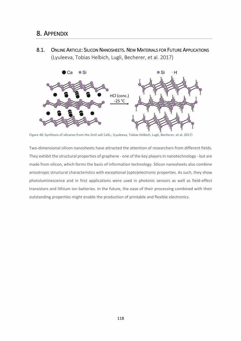
118
8. APPENDIX
8.1. ONLINE ARTICLE: SILICON NANOSHEETS. NEW MATERIALS FOR FUTURE APPLICATIONS
(Lyuleeva, Tobias Helbich, Lugli, Becherer, et al. 2017)
Figure 46: Synthesis of silicanes from the Zintl salt CaSi2. (Lyuleeva, Tobias Helbich, Lugli, Becherer, et al. 2017)
Two-dimensional silicon nanosheets have attracted the attention of researchers from different fields.
They exhibit the structural properties of graphene - one of the key players in nanotechnology - but are
made from silicon, which forms the basis of information technology. Silicon nanosheets also combine
anisotropic structural characteristics with exceptional (opto)electronic properties. As such, they show
photoluminescence and in first applications were used in photonic sensors as well as field-effect
transistors and lithium ion batteries. In the future, the ease of their processing combined with their
outstanding properties might enable the production of printable and flexible electronics.
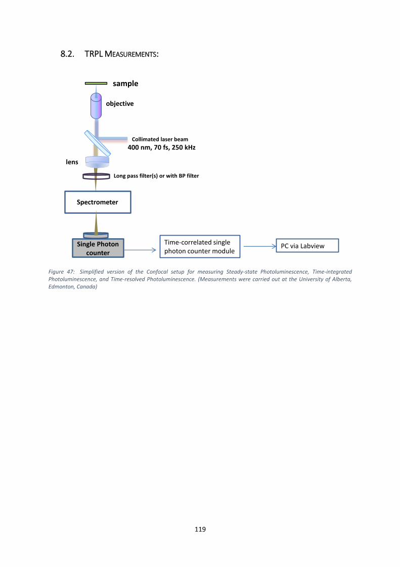
119
8.2. TRPL MEASUREMENTS:
Figure 47: Simplified version of the Confocal setup for measuring Steady-state Photoluminescence, Time-integrated Photoluminescence, and Time-resolved Photoluminescence. (Measurements were carried out at the University of Alberta, Edmonton, Canada)
Single Photon counter
Long pass filter(s) or with BP filter
Collimated laser beam
sample
Spectrometer
400 nm, 70 fs, 250 kHz
Time-correlated single photon counter module
PC via Labview
objective
lens
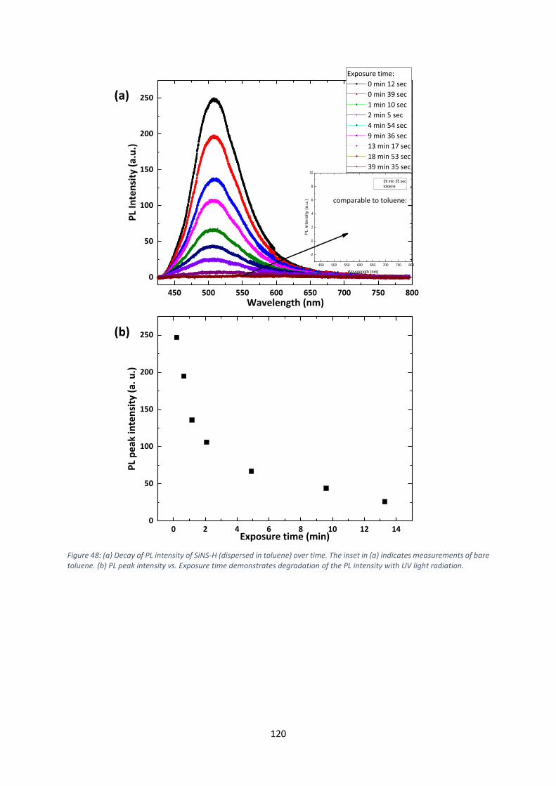
120
Figure 48: (a) Decay of PL intensity of SiNS-H (dispersed in toluene) over time. The inset in (a) indicates measurements of bare toluene. (b) PL peak intensity vs. Exposure time demonstrates degradation of the PL intensity with UV light radiation.
450 500 550 600 650 700 750 800
0
50
100
150
200
250
450 500 550 600 650 700 750 800
-2
0
2
4
6
8
10
39 min 35 sec
toloene
PL Inte
nsity (
a.u
.)
Wavelength (nm)
Exposure time:
0 min 12 sec
0 min 39 sec
1 min 10 sec
2 min 5 sec
4 min 54 sec
9 min 36 sec
13 min 17 sec
18 min 53 sec
39 min 35 sec
PL
Inte
nsi
ty (
a.u
.)
Wavelength (nm)
comparable to toluene:
0 2 4 6 8 10 12 140
50
100
150
200
250
PL
pe
ak in
ten
sity
(a.
u.)
Exposure time (min)
(a)
(b)
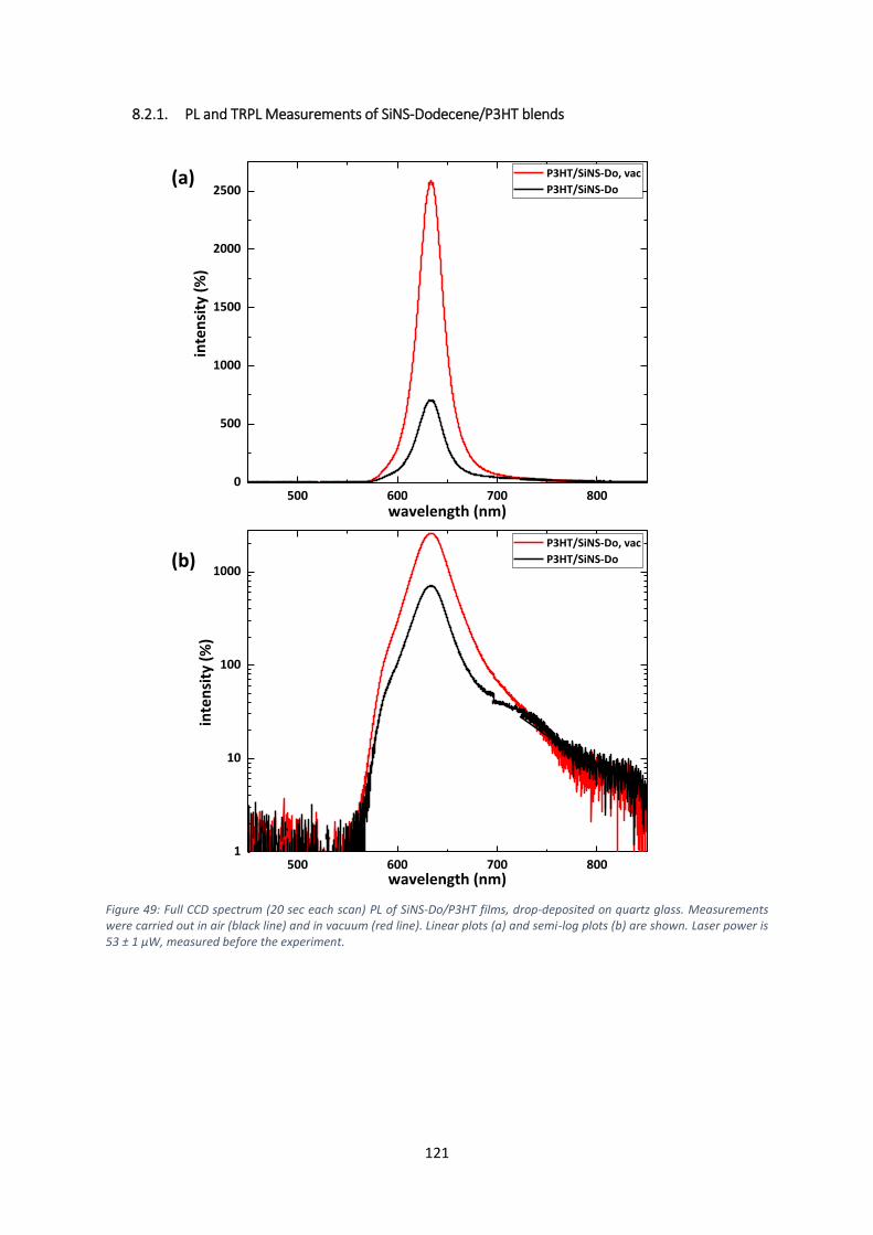
121
8.2.1. PL and TRPL Measurements of SiNS-Dodecene/P3HT blends
Figure 49: Full CCD spectrum (20 sec each scan) PL of SiNS-Do/P3HT films, drop-deposited on quartz glass. Measurements were carried out in air (black line) and in vacuum (red line). Linear plots (a) and semi-log plots (b) are shown. Laser power is 53 ± 1 µW, measured before the experiment.
500 600 700 8001
10
100
1000
inte
nsi
ty (
%)
wavelength (nm)
P3HT/SiNS-Do, vac
P3HT/SiNS-Do
500 600 700 8000
500
1000
1500
2000
2500in
ten
sity
(%
)
wavelength (nm)
P3HT/SiNS-Do, vac
P3HT/SiNS-Do(a)
(b)
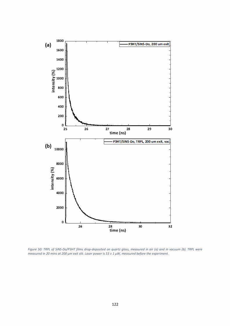
122
Figure 50: TRPL of SiNS-Do/P3HT films drop-deposited on quartz glass, measured in air (a) and in vacuum (b). TRPL were measured in 20 mins at 200 µm exit slit. Laser power is 53 ± 1 µW, measured before the experiment.
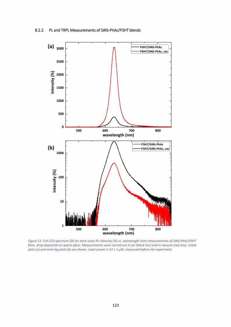
123
8.2.2. PL and TRPL Measurements of SiNS-PhAc/P3HT blends
Figure 51: Full CCD spectrum (20 sec each scan) PL intensity (%) vs. wavelength (nm) measurements of SiNS-PhAc/P3HT films, drop-deposited on quartz glass. Measurements were carried out in air (black line) and in vacuum (red line). Linear plots (a) and semi-log plots (b) are shown. Laser power is 53 ± 1 µW, measured before the experiment.
500 600 700 8000
500
1000
1500
2000
2500
3000in
ten
sity
(%
)
wavelength (nm)
P3HT/SiNS-PhAc
P3HT/SiNS-PhAc, vac
(a)
(b)
500 600 700 8001
10
100
1000
inte
nsi
ty (
%)
wavelength (nm)
P3HT/SiNS-PhAc
P3HT/SiNS-PhAc, vac
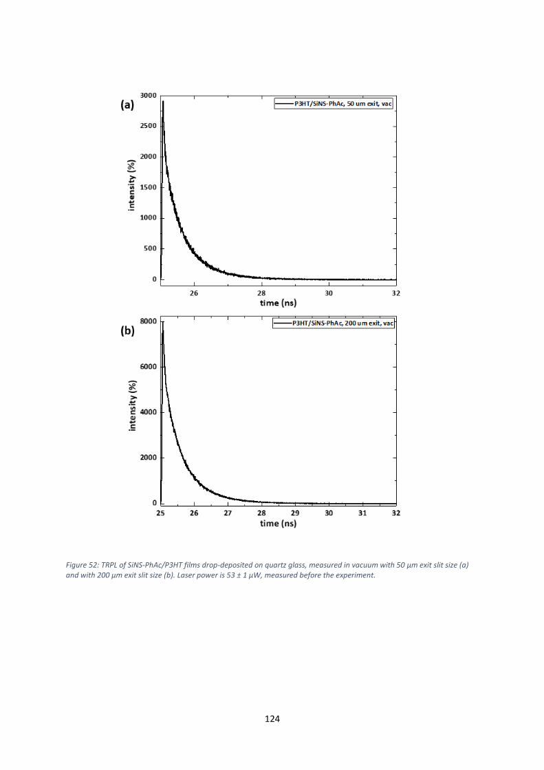
124
Figure 52: TRPL of SiNS-PhAc/P3HT films drop-deposited on quartz glass, measured in vacuum with 50 µm exit slit size (a) and with 200 µm exit slit size (b). Laser power is 53 ± 1 µW, measured before the experiment.
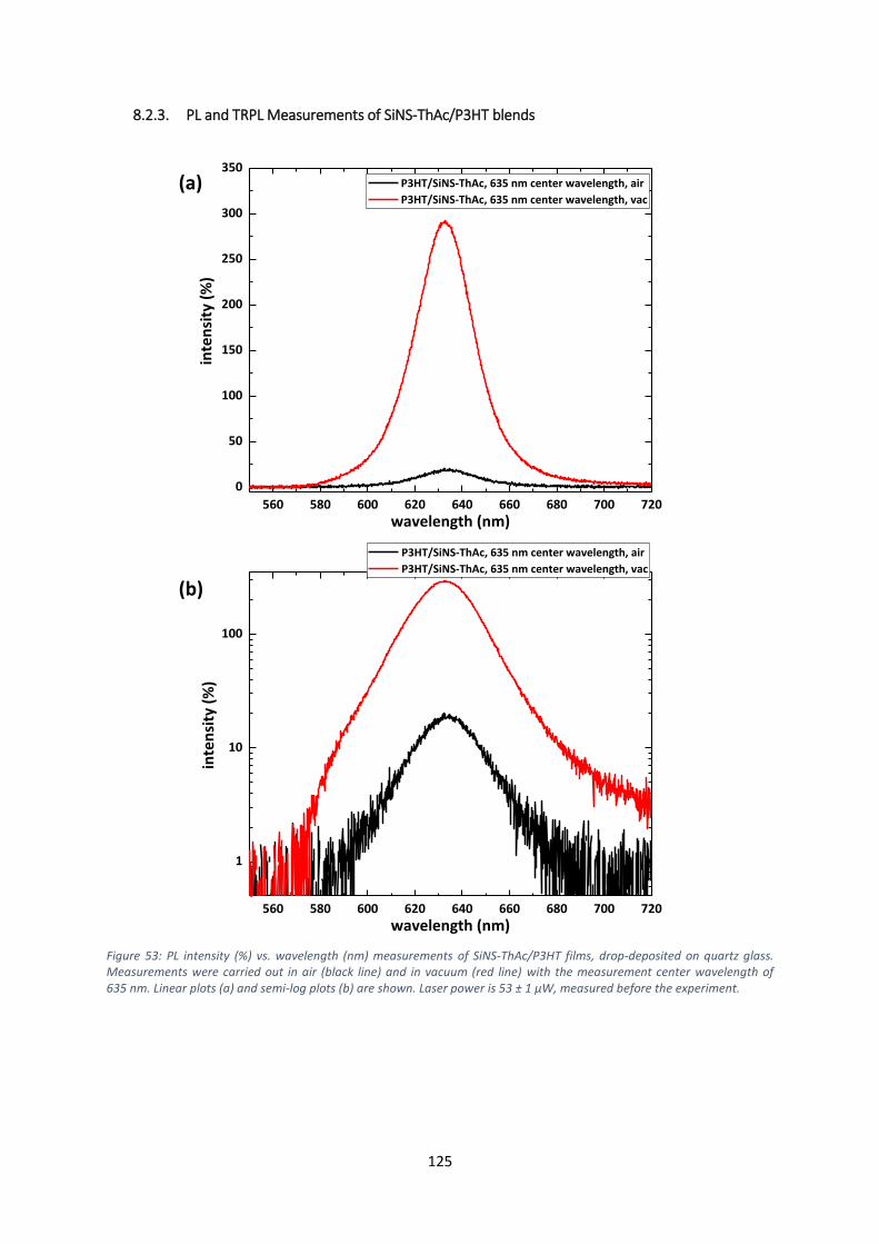
125
8.2.3. PL and TRPL Measurements of SiNS-ThAc/P3HT blends
Figure 53: PL intensity (%) vs. wavelength (nm) measurements of SiNS-ThAc/P3HT films, drop-deposited on quartz glass. Measurements were carried out in air (black line) and in vacuum (red line) with the measurement center wavelength of 635 nm. Linear plots (a) and semi-log plots (b) are shown. Laser power is 53 ± 1 µW, measured before the experiment.
560 580 600 620 640 660 680 700 720
0
50
100
150
200
250
300
350
inte
nsi
ty (
%)
wavelength (nm)
P3HT/SiNS-ThAc, 635 nm center wavelength, air
P3HT/SiNS-ThAc, 635 nm center wavelength, vac(a)
(b)
560 580 600 620 640 660 680 700 720
1
10
100
inte
nsi
ty (
%)
wavelength (nm)
P3HT/SiNS-ThAc, 635 nm center wavelength, air
P3HT/SiNS-ThAc, 635 nm center wavelength, vac
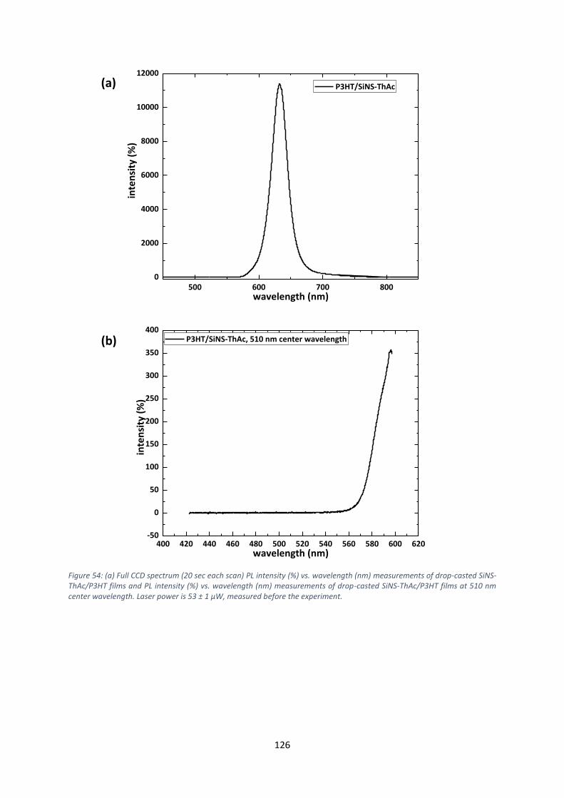
126
Figure 54: (a) Full CCD spectrum (20 sec each scan) PL intensity (%) vs. wavelength (nm) measurements of drop-casted SiNS-ThAc/P3HT films and PL intensity (%) vs. wavelength (nm) measurements of drop-casted SiNS-ThAc/P3HT films at 510 nm center wavelength. Laser power is 53 ± 1 µW, measured before the experiment.
400 420 440 460 480 500 520 540 560 580 600 620-50
0
50
100
150
200
250
300
350
400
inte
nsi
ty (
%)
wavelength (nm)
P3HT/SiNS-ThAc, 510 nm center wavelength
(a)
500 600 700 8000
2000
4000
6000
8000
10000
12000
inte
nsi
ty (
%)
wavelength (nm)
P3HT/SiNS-ThAc
(b)
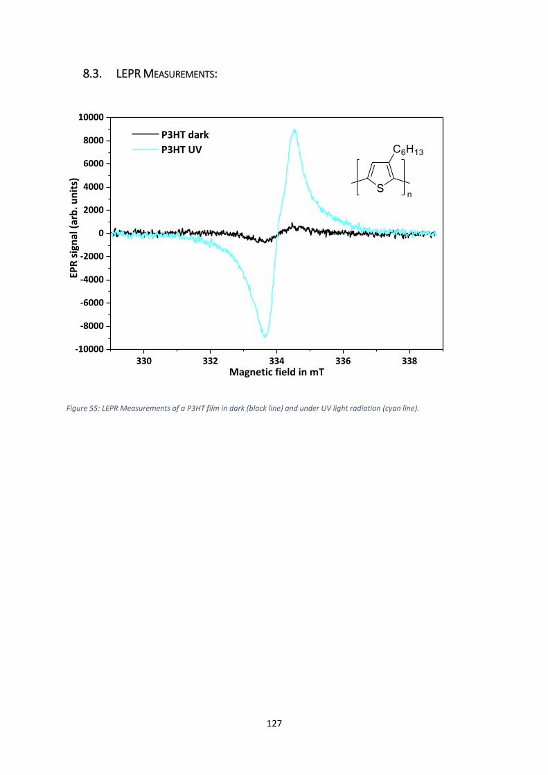
127
8.3. LEPR MEASUREMENTS:
Figure 55: LEPR Measurements of a P3HT film in dark (black line) and under UV light radiation (cyan line).
330 332 334 336 338-10000
-8000
-6000
-4000
-2000
0
2000
4000
6000
8000
10000
EPR
sig
nal
(ar
b. u
nit
s)
Magnetic field in mT
P3HT dark
P3HT UV
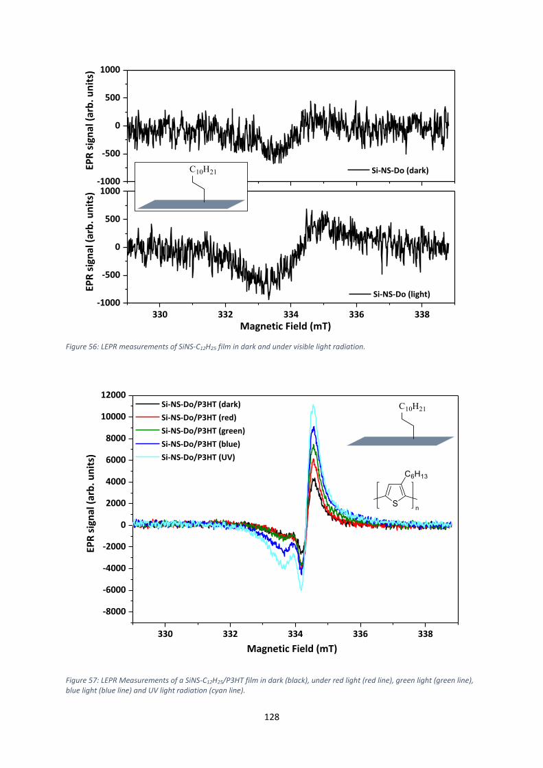
128
Figure 56: LEPR measurements of SiNS-C12H25 film in dark and under visible light radiation.
Figure 57: LEPR Measurements of a SiNS-C12H25/P3HT film in dark (black), under red light (red line), green light (green line), blue light (blue line) and UV light radiation (cyan line).
-1000
-500
0
500
1000
330 332 334 336 338-1000
-500
0
500
1000
EPR
sig
nal
(ar
b. u
nit
s)
Si-NS-Do (dark)
EPR
sig
nal
(ar
b. u
nit
s)
Magnetic Field (mT)
Si-NS-Do (light)
330 332 334 336 338
-8000
-6000
-4000
-2000
0
2000
4000
6000
8000
10000
12000
EPR
sig
nal
(ar
b. u
nit
s)
Magnetic Field (mT)
Si-NS-Do/P3HT (dark)
Si-NS-Do/P3HT (red)
Si-NS-Do/P3HT (green)
Si-NS-Do/P3HT (blue)
Si-NS-Do/P3HT (UV)
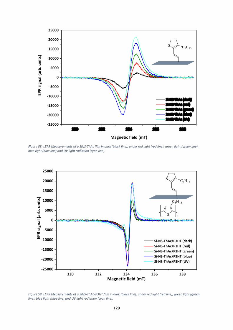
129
Figure 58: LEPR Measurements of a SiNS-ThAc film in dark (black line), under red light (red line), green light (green line), blue light (blue line) and UV light radiation (cyan line).
Figure 59: LEPR Measurements of a SiNS-ThAc/P3HT film in dark (black line), under red light (red line), green light (green line), blue light (blue line) and UV light radiation (cyan line).
330 332 334 336 338-25000
-20000
-15000
-10000
-5000
0
5000
10000
15000
20000
25000
Si-NS-ThAc (dark)
Si-NS-ThAc (red)
Si-NS-ThAc (green)
Si-NS-ThAc (blue)
Si-NS-ThAc (UV)
EPR
sig
nal
(ar
b. u
nit
s)
Magnetic field (mT)
330 332 334 336 338-25000
-20000
-15000
-10000
-5000
0
5000
10000
15000
20000
25000
EPR
sig
nal
(ar
b. u
nit
s)
Magnetic field (mT)
Si-NS-ThAc/P3HT (dark)
Si-NS-ThAc/P3HT (red)
Si-NS-ThAc/P3HT (green)
Si-NS-ThAc/P3HT (blue)
Si-NS-ThAc/P3HT (UV)
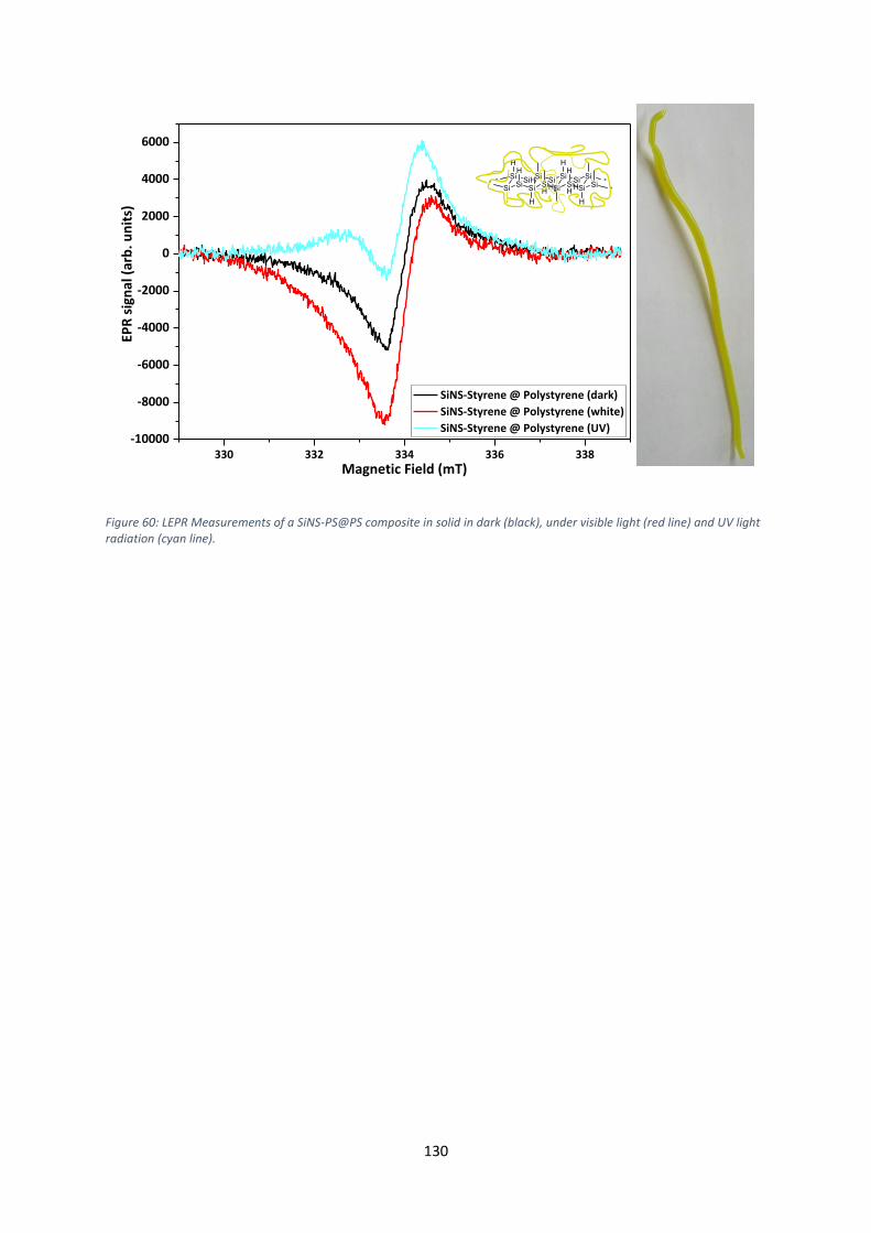
130
Figure 60: LEPR Measurements of a SiNS-PS@PS composite in solid in dark (black), under visible light (red line) and UV light radiation (cyan line).
330 332 334 336 338-10000
-8000
-6000
-4000
-2000
0
2000
4000
6000EP
R s
ign
al (
arb
. un
its)
Magnetic Field (mT)
SiNS-Styrene @ Polystyrene (dark)
SiNS-Styrene @ Polystyrene (white)
SiNS-Styrene @ Polystyrene (UV)
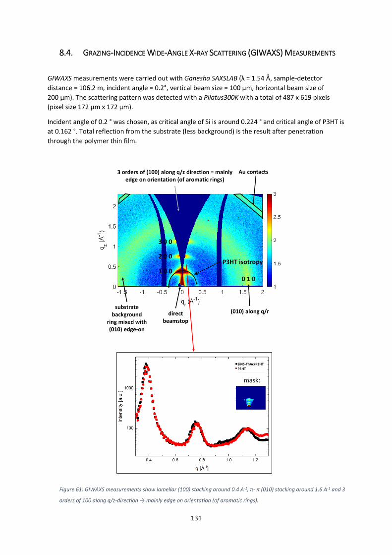
131
8.4. GRAZING-INCIDENCE WIDE-ANGLE X-RAY SCATTERING (GIWAXS) MEASUREMENTS
GIWAXS measurements were carried out with Ganesha SAXSLAB (λ = 1.54 Å, sample-detector
distance = 106.2 m, incident angle = 0.2°, vertical beam size = 100 µm, horizontal beam size of
200 µm). The scattering pattern was detected with a Pilatus300K with a total of 487 x 619 pixels
(pixel size 172 µm x 172 µm).
Incident angle of 0.2 ° was chosen, as critical angle of Si is around 0.224 ° and critical angle of P3HT is
at 0.162 °. Total reflection from the substrate (less background) is the result after penetration
through the polymer thin film.
Figure 61: GIWAXS measurements show lamellar (100) stacking around 0.4 A-1, π- π (010) stacking around 1.6 A-1 and 3
orders of 100 along q/z-direction → mainly edge on orientation (of aromatic rings).
Au contacts
directbeamstop
substratebackground
ring mixed with(010) edge-on
P3HT isotropy
0 1 0
(010) along q/r
3 orders of (100) along q/z direction = mainlyedge on orientation (of aromatic rings)
1 0 0
2 0 0
3 0 0
mask:
SiNS-ThAc/P3HTP3HT
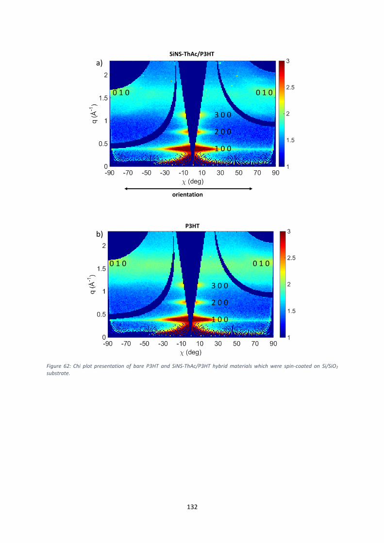
132
Figure 62: Chi plot presentation of bare P3HT and SiNS-ThAc/P3HT hybrid materials which were spin-coated on Si/SiO2 substrate.
SiNS-ThAc/P3HT
orientation
1 0 0
2 0 0
3 0 0
0 1 0 0 1 0
1 0 0
2 0 0
3 0 0
0 1 0 0 1 0
P3HT
a)
b)
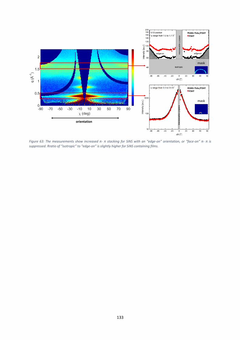
133
Figure 63: The measurements show increased π- π stacking for SiNS with an “edge-on” orientation, or “face-on” π- π is
suppressed. Rratio of “isotropic” to “edge-on” is slightly higher for SiNS containing films.
orientation
mask
mask
SiNS-ThAc/P3HTP3HT
SiNS-ThAc/P3HTP3HT
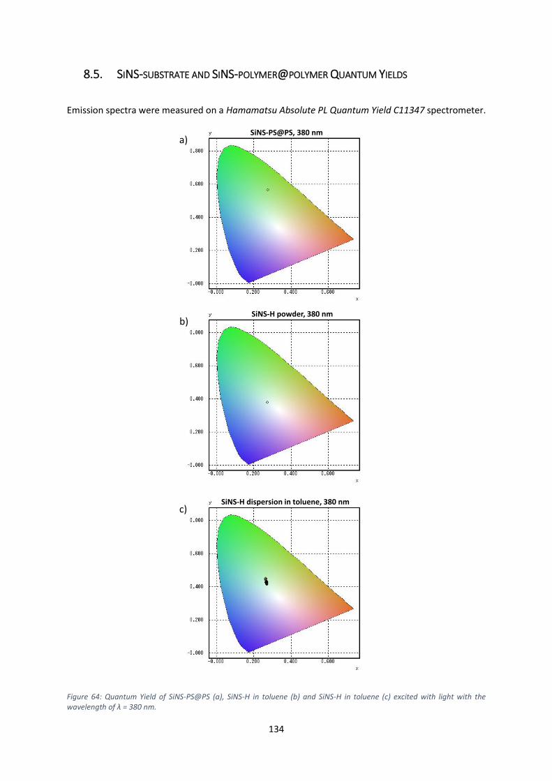
134
8.5. SINS-SUBSTRATE AND SINS-POLYMER@POLYMER QUANTUM YIELDS
Emission spectra were measured on a Hamamatsu Absolute PL Quantum Yield C11347 spectrometer.
Figure 64: Quantum Yield of SiNS-PS@PS (a), SiNS-H in toluene (b) and SiNS-H in toluene (c) excited with light with the wavelength of λ = 380 nm.
SiNS-PS@PS, 380 nma)
b)
c)
SiNS-H powder, 380 nm
SiNS-H dispersion in toluene, 380 nm

135
Table 5: Absolute Average Quantum Yield (%) of solution and solid samples.
SiNS-H (toluene)
SiNS-C12H25 (toluene)
SiNS-C12H25 (powder)
SiNS-PS@PS
0.98 2.10 0.91 2.33
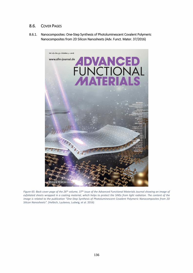
136
8.6. COVER PAGES
8.6.1. Nanocomposites: One-Step Synthesis of Photoluminescent Covalent Polymeric
Nanocomposites from 2D Silicon Nanosheets (Adv. Funct. Mater. 37/2016)
Figure 65: Back cover page of the 26th volume, 37th issue of the Advanced Functional Materials Journal showing an image of exfoliated sheets wrapped in a coating material, which helps to protect the SiNSs from light radiation. The content of the image is related to the publication “One-Step Synthesis of Photoluminescent Covalent Polymeric Nanocomposites from 2D Silicon Nanosheets”. (Helbich, Lyuleeva, Ludwig, et al. 2016)
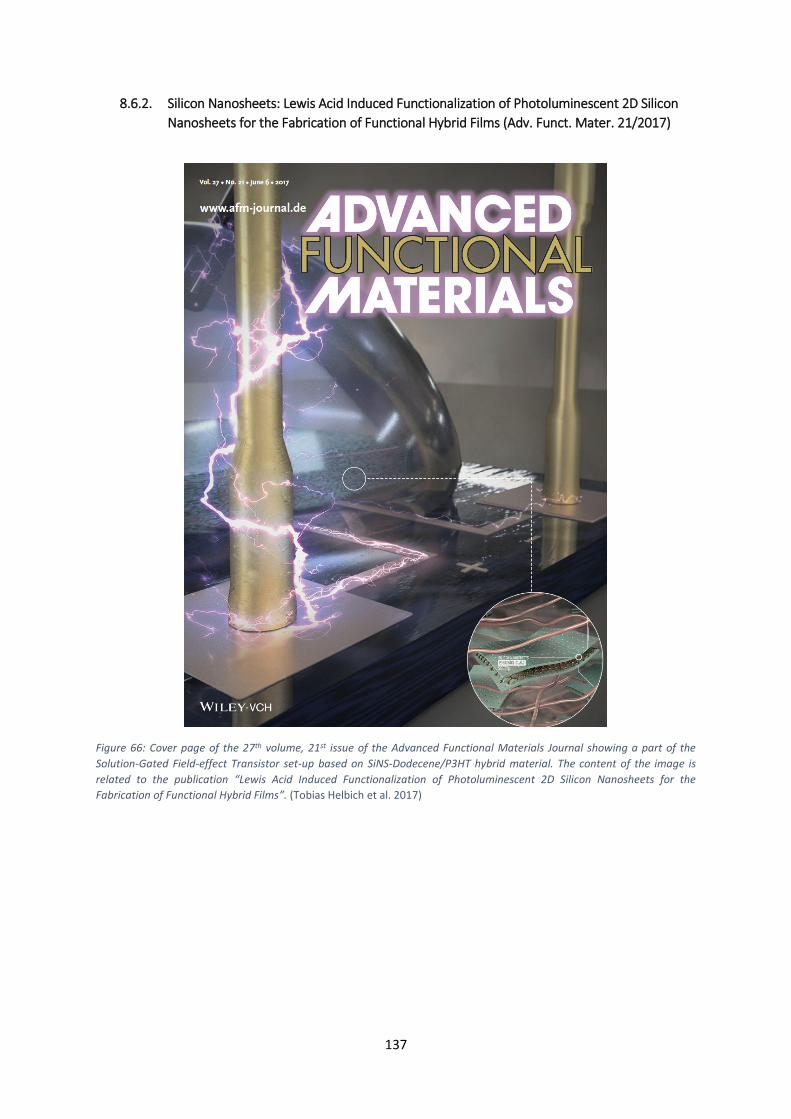
137
8.6.2. Silicon Nanosheets: Lewis Acid Induced Functionalization of Photoluminescent 2D Silicon
Nanosheets for the Fabrication of Functional Hybrid Films (Adv. Funct. Mater. 21/2017)
Figure 66: Cover page of the 27th volume, 21st issue of the Advanced Functional Materials Journal showing a part of the
Solution-Gated Field-effect Transistor set-up based on SiNS-Dodecene/P3HT hybrid material. The content of the image is
related to the publication “Lewis Acid Induced Functionalization of Photoluminescent 2D Silicon Nanosheets for the
Fabrication of Functional Hybrid Films”. (Tobias Helbich et al. 2017)

138
9. LICENSES FOR COPYRIGHT CONTENT
Agreement between: Samuel Wright; [email protected]
And: Lyuleeva, Alina
Date: 23 October 2017
Subject: RE: [Salesforce Web to Submission] General Contact Us Form
Dear Alina,
Yes, you can use the image. We would be very interested to receive an electronic copy of the thesis if
possible. Attached is a full resolution version of the image.
Thank you,
Best regards,
Samuel Wright, PhD
Application Engineer, 355 S. Technology Dr., Central Islip, NY 11722 Phone: (631) 981-7081 Fax: (631) 981-7095 www.cvdequipment.com enabling tomorrow’s technologies™ CVD Production R&D Processing Gas & Chemical Delivery

139
InTech's Publishing Ethics and Legal Affairs Department
Agreement between: Ivan Šuljić
And: Lyuleeva, Alina
Date: 24.10.2017
Dear Alina,
My name is Ivan Šuljić and I am writing you from InTech's Publishing Ethics and Legal Affairs
Department.
You may freely use the figure 5 in your publication as long as you cite the source chapter of the
original figure, and include the following notice in the figure caption:
© 2017 Pérez‐Taborda JA, Caballero-Calero O, Martín‐González M. Published in [short citation]
under CC BY 3.0 license. Available from: http://dx.doi.org/10.5772/67730.
Hopefully I managed to help you, but if you have any other questions feel free to contact me.
Kind regards,
Ivan Šuljić
Publishing Ethics and Legal Affairs
__________________________________ InTech - open science | open minds Email: [email protected] Website: www.intechopen.com Phone: +385 51 688 977 Fax: +385 51 686 166 Janeza Trdine 9 51000 Rijeka, Croatia The information contained in either this email and, if applicable, the attachment, are confidential and are intended only for the recipient. The contents of either the email or the attachment may not be disclosed publicly. If you are not the intended recipient(s), any use, disclosure, copying, or distribution is prohibited and may be unlawful. If you have received this communication in error, please notify us by e-mail at [email protected] then delete the e-mail and all attachments and any copies thereof. This communication is part of InTech's publishing activity and is not intended for unauthorized use or distribution.
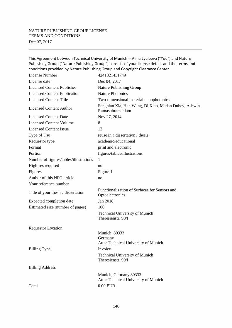
140
NATURE PUBLISHING GROUP LICENSE
TERMS AND CONDITIONS
Dec 07, 2017
This Agreement between Technical University of Munich -- Alina Lyuleeva ("You") and Nature Publishing Group ("Nature Publishing Group") consists of your license details and the terms and conditions provided by Nature Publishing Group and Copyright Clearance Center.
License Number 4241821431749
License date Dec 04, 2017
Licensed Content Publisher Nature Publishing Group
Licensed Content Publication Nature Photonics
Licensed Content Title Two-dimensional material nanophotonics
Licensed Content Author Fengnian Xia, Han Wang, Di Xiao, Madan Dubey, Ashwin
Ramasubramaniam
Licensed Content Date Nov 27, 2014
Licensed Content Volume 8
Licensed Content Issue 12
Type of Use reuse in a dissertation / thesis
Requestor type academic/educational
Format print and electronic
Portion figures/tables/illustrations
Number of figures/tables/illustrations 1
High-res required no
Figures Figure 1
Author of this NPG article no
Your reference number
Title of your thesis / dissertation Functionalization of Surfaces for Sensors and
Optoelectronics
Expected completion date Jan 2018
Estimated size (number of pages) 100
Requestor Location
Technical University of Munich
Theresienstr. 90/I
Munich, 80333
Germany
Attn: Technical University of Munich
Billing Type Invoice
Billing Address
Technical University of Munich
Theresienstr. 90/I
Munich, Germany 80333
Attn: Technical University of Munich
Total 0.00 EUR

141
JOHN WILEY AND SONS LICENSE
TERMS AND CONDITIONS
Dec 07, 2017
This Agreement between Technical University of Munich -- Alina Lyuleeva ("You") and John Wiley and Sons ("John Wiley and Sons") consists of your license details and the terms and conditions provided by John Wiley and Sons and Copyright Clearance Center.
License Number 4214860451517
License date Oct 23, 2017
Licensed Content Publisher John Wiley and Sons
Licensed Content Publication Advanced Functional Materials
Licensed Content Title
One-Step Synthesis of Photoluminescent
Covalent Polymeric Nanocomposites from
2D Silicon Nanosheets
Licensed Content Author
Tobias Helbich,Alina Lyuleeva,Theresa
Ludwig,Lavinia M. Scherf,Thomas F.
Fässler,Paolo Lugli,Bernhard Rieger
Licensed Content Date Jul 28, 2016
Licensed Content Pages 8
Type of use Dissertation/Thesis
Requestor type University/Academic
Format Print and electronic
Portion Figure/table
Number of figures/tables 5
Original Wiley figure/table number(s) Figure S2
Will you be translating? No
Title of your thesis / dissertation Functionalization of Surfaces for Sensors
and Optoelectronics
Expected completion date Jan 2018
Expected size (number of pages) 100
Requestor Location
Technical University of Munich
Theresienstr. 90/I
Munich, 80333
Germany
Attn: Technical University of Munich
Publisher Tax ID EU826007151
Billing Type Invoice
Billing Address
Technical University of Munich
Theresienstr. 90/I
Munich, Germany 80333
Attn: Technical University of Munich
Total 0.00 USD
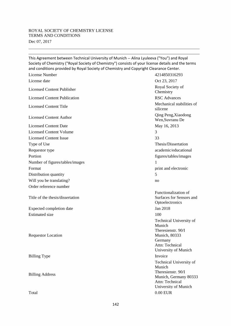
142
ROYAL SOCIETY OF CHEMISTRY LICENSE
TERMS AND CONDITIONS
Dec 07, 2017
This Agreement between Technical University of Munich -- Alina Lyuleeva ("You") and Royal Society of Chemistry ("Royal Society of Chemistry") consists of your license details and the terms and conditions provided by Royal Society of Chemistry and Copyright Clearance Center.
License Number 4214850316293
License date Oct 23, 2017
Licensed Content Publisher Royal Society of
Chemistry
Licensed Content Publication RSC Advances
Licensed Content Title Mechanical stabilities of
silicene
Licensed Content Author Qing Peng,Xiaodong
Wen,Suvranu De
Licensed Content Date May 16, 2013
Licensed Content Volume 3
Licensed Content Issue 33
Type of Use Thesis/Dissertation
Requestor type academic/educational
Portion figures/tables/images
Number of figures/tables/images 1
Format print and electronic
Distribution quantity 5
Will you be translating? no
Order reference number
Title of the thesis/dissertation
Functionalization of
Surfaces for Sensors and
Optoelectronics
Expected completion date Jan 2018
Estimated size 100
Requestor Location
Technical University of
Munich
Theresienstr. 90/I
Munich, 80333
Germany
Attn: Technical
University of Munich
Billing Type Invoice
Billing Address
Technical University of
Munich
Theresienstr. 90/I
Munich, Germany 80333
Attn: Technical
University of Munich
Total 0.00 EUR
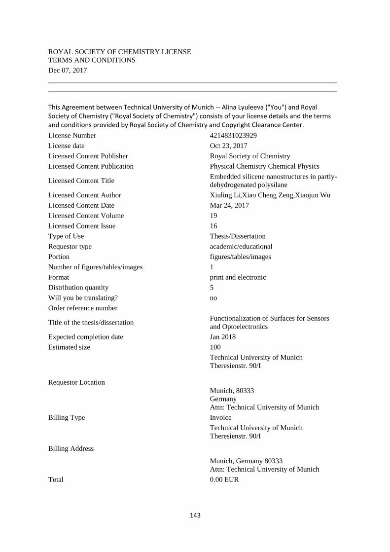
143
ROYAL SOCIETY OF CHEMISTRY LICENSE
TERMS AND CONDITIONS
Dec 07, 2017
This Agreement between Technical University of Munich -- Alina Lyuleeva ("You") and Royal Society of Chemistry ("Royal Society of Chemistry") consists of your license details and the terms and conditions provided by Royal Society of Chemistry and Copyright Clearance Center.
License Number 4214831023929
License date Oct 23, 2017
Licensed Content Publisher Royal Society of Chemistry
Licensed Content Publication Physical Chemistry Chemical Physics
Licensed Content Title Embedded silicene nanostructures in partly-
dehydrogenated polysilane
Licensed Content Author Xiuling Li,Xiao Cheng Zeng,Xiaojun Wu
Licensed Content Date Mar 24, 2017
Licensed Content Volume 19
Licensed Content Issue 16
Type of Use Thesis/Dissertation
Requestor type academic/educational
Portion figures/tables/images
Number of figures/tables/images 1
Format print and electronic
Distribution quantity 5
Will you be translating? no
Order reference number
Title of the thesis/dissertation Functionalization of Surfaces for Sensors
and Optoelectronics
Expected completion date Jan 2018
Estimated size 100
Requestor Location
Technical University of Munich
Theresienstr. 90/I
Munich, 80333
Germany
Attn: Technical University of Munich
Billing Type Invoice
Billing Address
Technical University of Munich
Theresienstr. 90/I
Munich, Germany 80333
Attn: Technical University of Munich
Total 0.00 EUR
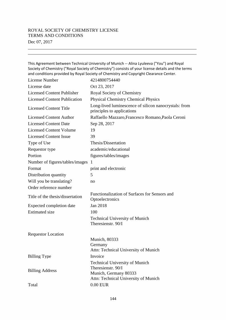
144
ROYAL SOCIETY OF CHEMISTRY LICENSE
TERMS AND CONDITIONS
Dec 07, 2017
This Agreement between Technical University of Munich -- Alina Lyuleeva ("You") and Royal Society of Chemistry ("Royal Society of Chemistry") consists of your license details and the terms and conditions provided by Royal Society of Chemistry and Copyright Clearance Center.
License Number 4214800754440
License date Oct 23, 2017
Licensed Content Publisher Royal Society of Chemistry
Licensed Content Publication Physical Chemistry Chemical Physics
Licensed Content Title Long-lived luminescence of silicon nanocrystals: from
principles to applications
Licensed Content Author Raffaello Mazzaro,Francesco Romano,Paola Ceroni
Licensed Content Date Sep 28, 2017
Licensed Content Volume 19
Licensed Content Issue 39
Type of Use Thesis/Dissertation
Requestor type academic/educational
Portion figures/tables/images
Number of figures/tables/images 1
Format print and electronic
Distribution quantity 5
Will you be translating? no
Order reference number
Title of the thesis/dissertation Functionalization of Surfaces for Sensors and
Optoelectronics
Expected completion date Jan 2018
Estimated size 100
Requestor Location
Technical University of Munich
Theresienstr. 90/I
Munich, 80333
Germany
Attn: Technical University of Munich
Billing Type Invoice
Billing Address
Technical University of Munich
Theresienstr. 90/I
Munich, Germany 80333
Attn: Technical University of Munich
Total 0.00 EUR
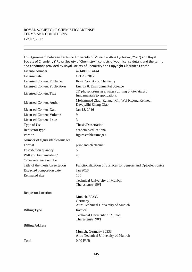
145
ROYAL SOCIETY OF CHEMISTRY LICENSE
TERMS AND CONDITIONS
Dec 07, 2017
This Agreement between Technical University of Munich -- Alina Lyuleeva ("You") and Royal Society of Chemistry ("Royal Society of Chemistry") consists of your license details and the terms and conditions provided by Royal Society of Chemistry and Copyright Clearance Center.
License Number 4214800514144
License date Oct 23, 2017
Licensed Content Publisher Royal Society of Chemistry
Licensed Content Publication Energy & Environmental Science
Licensed Content Title 2D phosphorene as a water splitting photocatalyst:
fundamentals to applications
Licensed Content Author Mohammad Ziaur Rahman,Chi Wai Kwong,Kenneth
Davey,Shi Zhang Qiao
Licensed Content Date Jan 18, 2016
Licensed Content Volume 9
Licensed Content Issue 3
Type of Use Thesis/Dissertation
Requestor type academic/educational
Portion figures/tables/images
Number of figures/tables/images 1
Format print and electronic
Distribution quantity 5
Will you be translating? no
Order reference number
Title of the thesis/dissertation Functionalization of Surfaces for Sensors and Optoelectronics
Expected completion date Jan 2018
Estimated size 100
Requestor Location
Technical University of Munich
Theresienstr. 90/I
Munich, 80333
Germany
Attn: Technical University of Munich
Billing Type Invoice
Billing Address
Technical University of Munich
Theresienstr. 90/I
Munich, Germany 80333
Attn: Technical University of Munich
Total 0.00 EUR
146
Confirmation Number: 11685753 Order Date: 12/07/2017 Journal of Physics D: Applied Physics
• Order detail ID: 70841986 • Order License Id: 4243570741971 • ISSN: 0022-3727 • Publication Type: Journal • Volume: • Issue: • Start page: • Publisher: IOP Publishing • Permission Status: Granted • Permission type: Republish or display content • Type of use: Thesis/Dissertation
Requestor type Author of requested content
Format Print, Electronic
Portion image/photo
Number of images/photos
requested 5
The requesting
person/organization Alina Lyuleeva
Title or numeric reference of the
portion(s) Article
Title of the article or chapter the
portion is from N/A
Editor of portion(s) N/A
Author of portion(s) Alina Lyuleeva
Volume of serial or monograph N/A
Page range of portion N/A
Publication date of portion Jan 2018
Rights for Main product and any product related to
main product
Duration of use Life of current edition
Creation of copies for the disabled no
With minor editing privileges yes
For distribution to Worldwide
In the following language(s) Original language of publication
With incidental promotional use no
Lifetime unit quantity of new
product Up to 499
Title Functionalization of Surfaces for Sensors
and Optoelectronics
Instructor name n/a
Institution name n/a
Expected presentation date Jan 2018
147
JOHN WILEY AND SONS LICENSE
TERMS AND CONDITIONS
Dec 19, 2017
This Agreement between Technical University of Munich -- Alina Lyuleeva ("You") and John Wiley and Sons ("John Wiley and Sons") consists of your license details and the terms and conditions provided by John Wiley and Sons and Copyright Clearance Center.
License Number 4252470548938
License date Dec 19, 2017
Licensed Content
Publisher John Wiley and Sons
Licensed Content
Publication Advanced Functional Materials
Licensed Content Title
Nanocomposites: One-Step Synthesis of Photoluminescent Covalent
Polymeric Nanocomposites from 2D Silicon Nanosheets (Adv. Funct.
Mater. 37/2016)
Licensed Content
Author
Tobias Helbich,Alina Lyuleeva,Theresa Ludwig,Lavinia M.
Scherf,Thomas F. Fässler,Paolo Lugli,Bernhard Rieger
Licensed Content Date Oct 4, 2016
Licensed Content Pages 1
Type of use Dissertation/Thesis
Requestor type Author of this Wiley article
Format Print and electronic
Portion Figure/table
Number of
figures/tables 1
Original Wiley
figure/table number(s) Back Cover
Will you be translating? No
Title of your thesis /
dissertation Functionalization of Surfaces for Sensors and Optoelectronics
Expected completion
date Jan 2018
Expected size (number
of pages) 100
Requestor Location
Technical University of Munich
Theresienstr. 90/I
Munich, 80333
Germany
Attn: Technical University of Munich
Publisher Tax ID EU826007151
Billing Type Invoice
Billing Address
Technical University of Munich
Theresienstr. 90/I
Munich, Germany 80333
Attn: Technical University of Munich
Total 0.00 EUR
148
JOHN WILEY AND SONS LICENSE
TERMS AND CONDITIONS
Dec 20, 2017
This Agreement between Technical University of Munich -- Alina Lyuleeva ("You") and John Wiley and Sons ("John Wiley and Sons") consists of your license details and the terms and conditions provided by John Wiley and Sons and Copyright Clearance Center.
License Number 4252980299360
License date Dec 20, 2017
Licensed Content
Publisher John Wiley and Sons
Licensed Content
Publication Advanced Functional Materials
Licensed Content Title
Silicon Nanosheets: Lewis Acid Induced Functionalization of Photoluminescent 2D
Silicon Nanosheets for the Fabrication of Functional Hybrid Films (Adv. Funct.
Mater. 21/2017)
Licensed Content
Author
Tobias Helbich,Alina Lyuleeva,Philipp Marx,Lavinia M. Scherf,Tapas K.
Purkait,Thomas F. Fässler,Paolo Lugli,Jonathan G. C. Veinot,Bernhard Rieger
Licensed Content Date Jun 5, 2017
Licensed Content Pages 1
Type of use Dissertation/Thesis
Requestor type Author of this Wiley article
Format Print and electronic
Portion Figure/table
Number of
figures/tables 1
Original Wiley
figure/table number(s) Front Cover
Will you be translating? No
Title of your thesis /
dissertation Functionalization of Surfaces for Sensors and Optoelectronics
Expected completion
date Jan 2018
Expected size (number
of pages) 100
Requestor Location
Technical University of Munich
Theresienstr. 90/I
Munich, 80333
Germany
Attn: Technical University of Munich
Publisher Tax ID EU826007151
Billing Type Invoice
Billing Address
Technical University of Munich
Theresienstr. 90/I
Munich, Germany 80333
Attn: Technical University of Munich
Total 0.00 EUR

149
– The End? –


![Sensors and Actuators B: Chemical - lasun-jlu.cn … · and biosystems with various functions [1,2,4–8]. Especially, the convenient functionalization with detecting probes [1,7],](https://img.pdfslide.net/doc/110x75/5ec44967c7c998789d2e9da5/sensors-and-actuators-b-chemical-lasun-jlucn-and-biosystems-with-various.jpg)