Embed Size (px)
Citation preview
Fundamental concepts ofFundamental concepts ofintegrated-circuit technologyintegrated-circuit technology
M. Rudan
University of Bologna

University of Bologna
Fundamental concepts of integrated-circuit technology M. Rudan
SILICON PLANAR TECHNOLOGY
10 in = 25.40 cm12 in = 30.48 cm
300 μm = 0.3 mm
Wafer
Chip

University of Bologna
Fundamental concepts of integrated-circuit technology M. Rudan
SILICON PLANAR TECHNOLOGY
300 μm = 0.3 mm
10 ÷ 20 μm
Bulk
Devices

University of Bologna
Fundamental concepts of integrated-circuit technology M. Rudan
N-TYPE DOPING (I)
10 ÷ 20 μm
Bulk
Adding suitably-chosen atoms increases the local concentration of free charge
n+

University of Bologna
Fundamental concepts of integrated-circuit technology M. Rudan
N-TYPE DOPING (II)
10 ÷ 20 μm
Bulk
Typically, the wafer is also lightly doped (from factory)
n+
n silicon (n- silicon)

University of Bologna
Fundamental concepts of integrated-circuit technology M. Rudan
N-TYPE DOPING (III)
The conductivity of pure (intrinsic) silicon (Si) is low: the material is a semiconductor. It is a IV-type material.
The addition of a small amount of V-type material, like phosphorus (P), arsenic (As), or antimony (Sb) increases the local concentration of free electrons.
The added materials are called dopants or impurities, of donor type.
The doped silicon is called extrinsic of n-type. It is not a chemical compound, e.g., of Si and P.

University of Bologna
Fundamental concepts of integrated-circuit technology M. Rudan
N-TYPE DOPING (IV)
The larger concentration of free electrons makes the local electrical conductivity to increase.
In an intrinsic semiconductor the electrical conductivity increases as temperature increases (opposite to conductors).
In a doped semiconductor the conductivity becomes independent of temperature at least in a range of temperatures.
The inclusion of dopants makes it possible to externally control the electrical conductivity.

University of Bologna
Fundamental concepts of integrated-circuit technology M. Rudan
P-TYPE DOPING (I)
The semiconductors allow for another type of doping, “dual” with respect to the n-type.
The addition of a small amount of III-type dopants, like boron (B), aluminum (Al), gallium (Ga), or Indium (In) increases the local concentration of free positive charges, called holes.
The doped silicon is called extrinsic of p-type. The dopants are of the acceptor type.
Holes are fictitious particles. The particles that actually carry the current are always electrons.
University of Bologna
Fundamental concepts of integrated-circuit technology M. Rudan
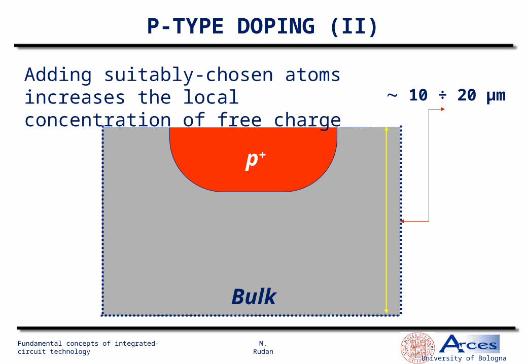
P-TYPE DOPING (II)
10 ÷ 20 μm
Bulk
Adding suitably-chosen atoms increases the local concentration of free charge
p+

University of Bologna
Fundamental concepts of integrated-circuit technology M. Rudan
P-TYPE DOPING (III)
The larger concentration of free holes makes the local electrical conductivity to increase.
Also in a p-type doped semiconductor the conductivity becomes independent of temperature at least in a range of temperatures.
The inclusion of n-type or p-type dopants makes it possible to externally control the electrical conductivity and also to obtain regions with a different type of dominant free charge.
University of Bologna
Fundamental concepts of integrated-circuit technology M. Rudan
N- AND P-TYPE DOPING
The electrons and holes are also collectively called carriers.
In an n-type region, the electrons are called majority carriers. A few holes are also present, that are called minority carriers.
In a p-type region, the holes are called majority carriers. A few electrons are also present, that are called minority carriers.
Under the influence of a given electric field, electrons and holes are accelerated in opposite directions.

University of Bologna
Fundamental concepts of integrated-circuit technology M. Rudan
P-TYPE DOPING (IV)
10 ÷ 20 μm
Bulk
p+
Typically, the wafer is also lightly doped (from factory)
p silicon (p- silicon)

University of Bologna
Fundamental concepts of integrated-circuit technology M. Rudan
P-N JUNCTION (I)
10 ÷ 20 μm
Bulk
p+
Two adjacent regions with opposite doping form a p-n junction.
n silicon (n- silicon)

University of Bologna
Fundamental concepts of integrated-circuit technology M. Rudan
P-N JUNCTION (II)
10 ÷ 20 μm
Bulk
n+
p silicon (p- silicon)
Two adjacent regions with opposite doping form a p-n junction.

University of Bologna
Fundamental concepts of integrated-circuit technology M. Rudan
P-SUBSTRATE MOS CAPACITOR
p silicon (bulk)
VG = 0
SiO2 (insulator)
Gate and bulk contactsVG > 0
Layer of electrons
Layer of missing electrons
The drawing is not in scale.

University of Bologna
Fundamental concepts of integrated-circuit technology M. Rudan
N-SUBSTRATE MOS CAPACITOR
n silicon (bulk)
VG = 0
SiO2 (insulator)
Gate and bulk contactsVG < 0
Layer of holes
Layer of electrons
The drawing is not in scale.

University of Bologna
Fundamental concepts of integrated-circuit technology M. Rudan
N-CHANNEL MOS TRANSISTOR (MOSFET)
p silicon (bulk)
VGB = 0
Gate and bulk contactsVGB > 0
Layer of electrons
Layer of missing electrons
The drawing is not in scale.
SiO2 (insulator)Source DrainConductive channel

University of Bologna
Fundamental concepts of integrated-circuit technology M. Rudan
P-CHANNEL MOS TRANSISTOR (MOSFET)
n silicon (bulk)
VGB = 0
Gate and bulk contactsVGB < 0
Layer of holes
Layer of electrons
The drawing is not in scale.
SiO2 (insulator)Source DrainConductive channel