Embed Size (px)
Citation preview
Fundamentals and Applications of Vacuum Microelectronics
Zhuowen SunEE 698A
Outline
• Introduction• Field emission basics• Spindt emitters and arrays• Beyond Spindt emitters • Field emission display• Summary
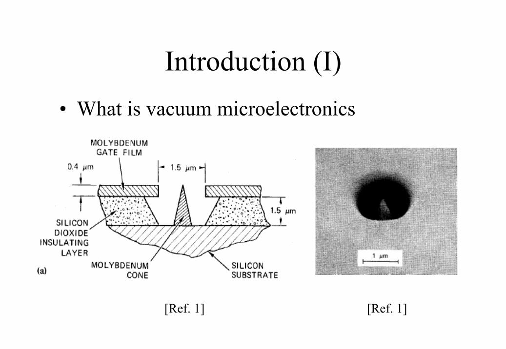
Introduction (I)• What is vacuum microelectronics
[Ref. 1] [Ref. 1]
Introduction (II)• Good
Power handling abilityBallistic and coherent transport Resistance to radiation-induced defects
• BadFabrication difficultiesPackaging issues
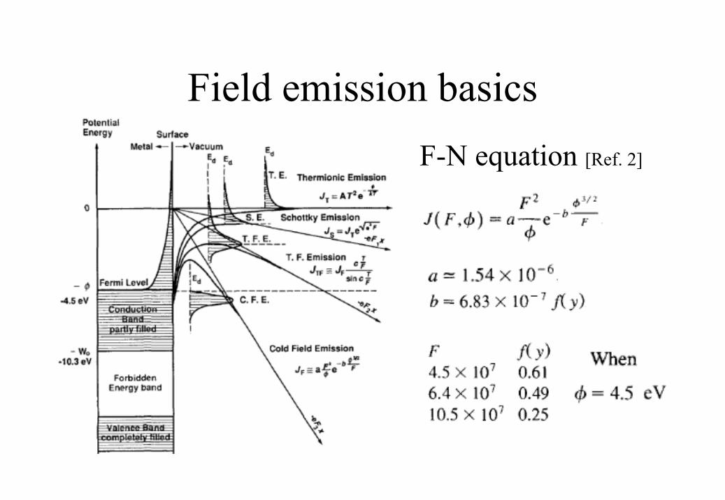
Field emission basicsF-N equation [Ref. 2]
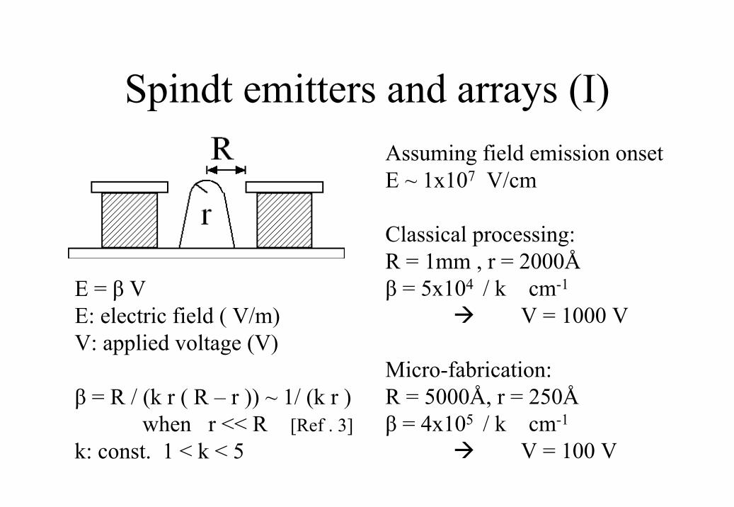
Spindt emitters and arrays (I)
E = β V E: electric field ( V/m) V: applied voltage (V)
β = R / (k r ( R – r )) ~ 1/ (k r ) when r << R [Ref . 3]
k: const. 1 < k < 5
Assuming field emission onsetE ~ 1x10⁷ V/cm
Classical processing:R = 1mm , r = 2000Åβ = 5x10⁴ / k cm-1
V = 1000 V
Micro-fabrication:R = 5000Å, r = 250Åβ = 4x10⁵ / k cm-1
V = 100 V
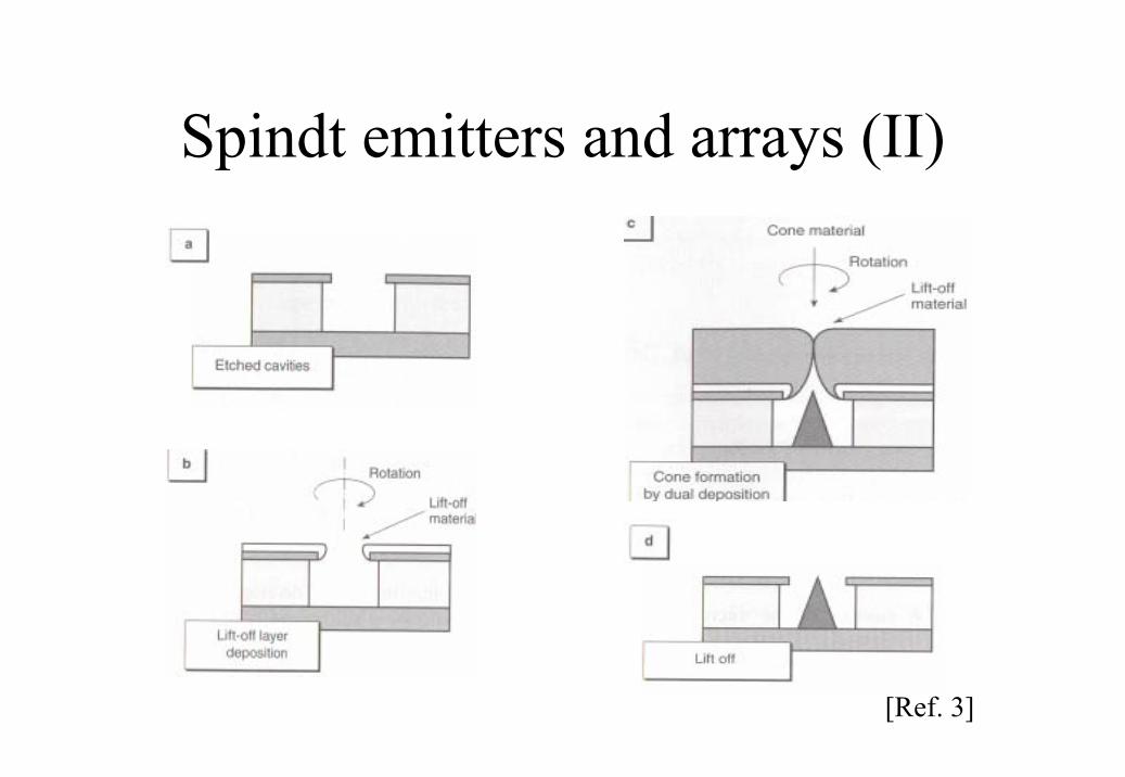
Spindt emitters and arrays (II)
[Ref. 3]
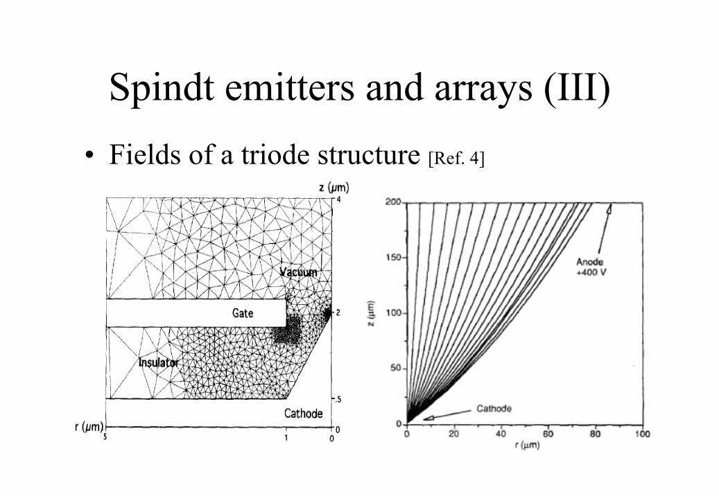
Spindt emitters and arrays (III)• Fields of a triode structure [Ref. 4]
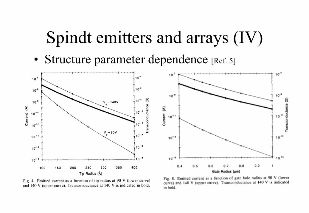
Spindt emitters and arrays (IV)• Structure parameter dependence [Ref. 5]
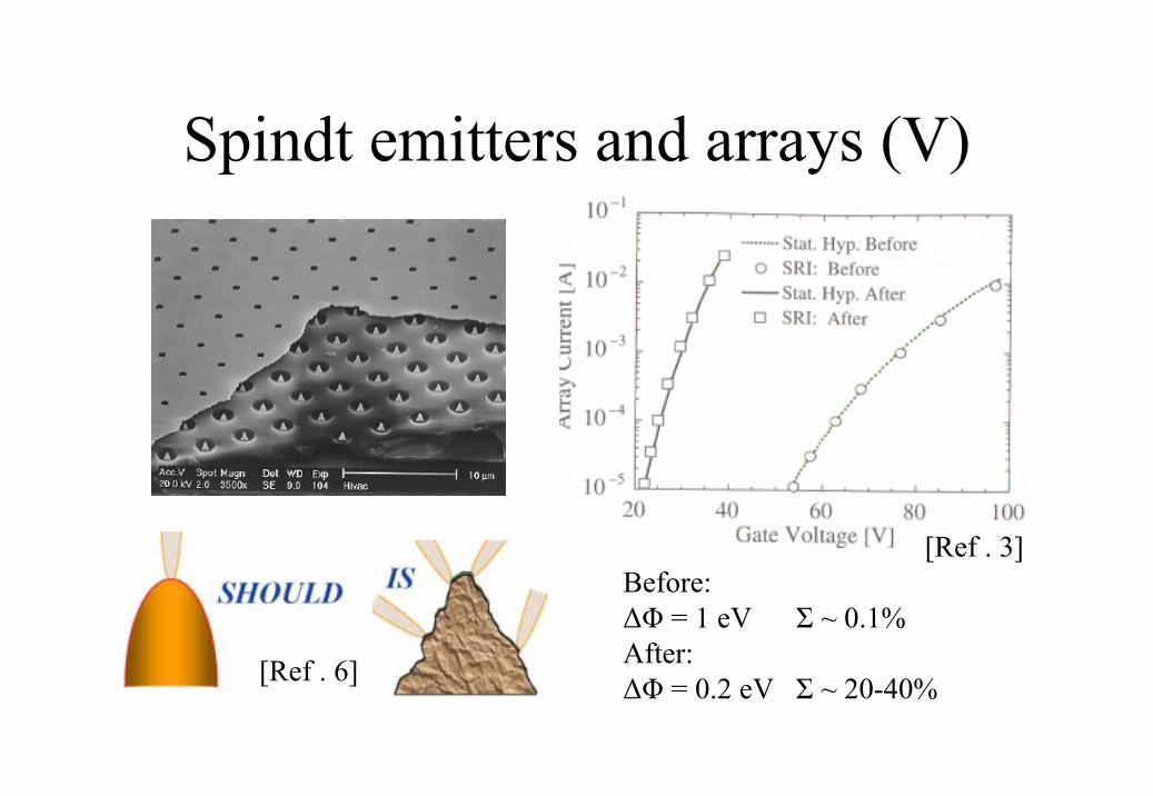
Spindt emitters and arrays (V)
Before:∆Φ = 1 eV Σ ~ 0.1%After:∆Φ = 0.2 eV Σ ~ 20-40%
[Ref . 3]
[Ref . 6]
Beyond Spindt emitters (I)
• Problems with simple Spindt emittersContaminationFocusingUniformity of array fabricationPower consumption
Beyond Spindt emitters (II)
• SolutionsMetal-Insulator-Metal (MIM) emittersSurface Conduction Emitters (SCE)Diamond-coated emittersCarbon nanotube emitters
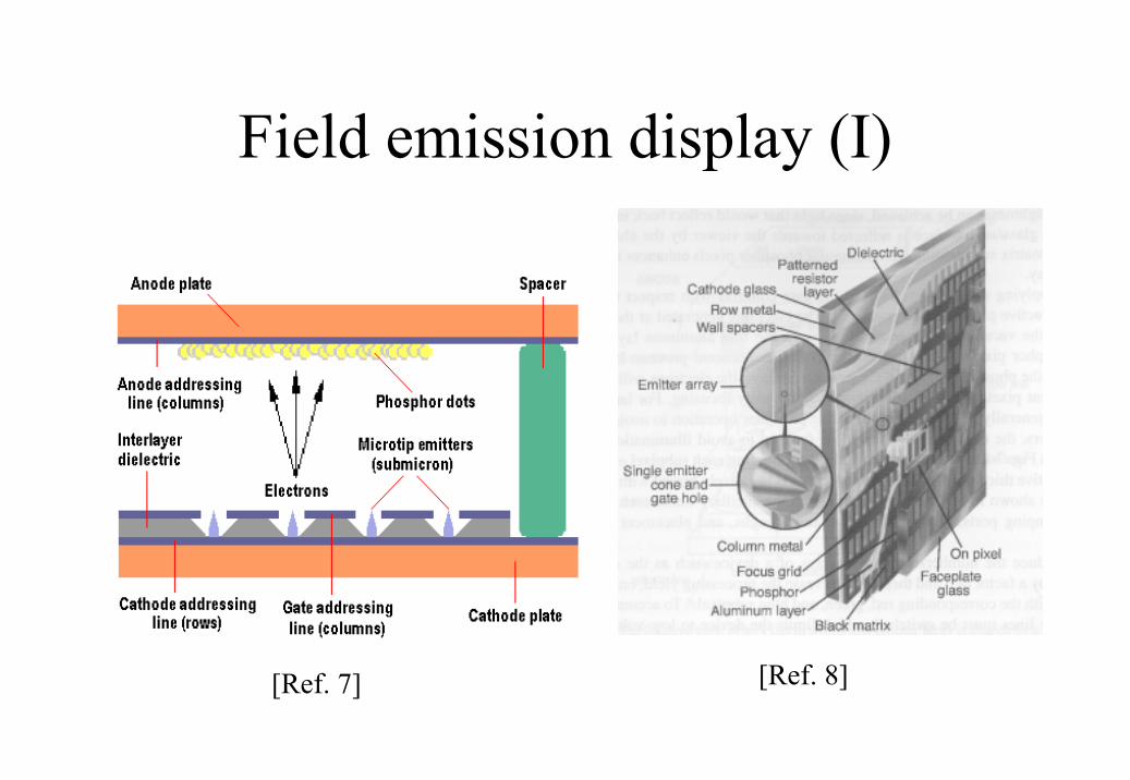
Field emission display (I)
[Ref. 7] [Ref. 8]
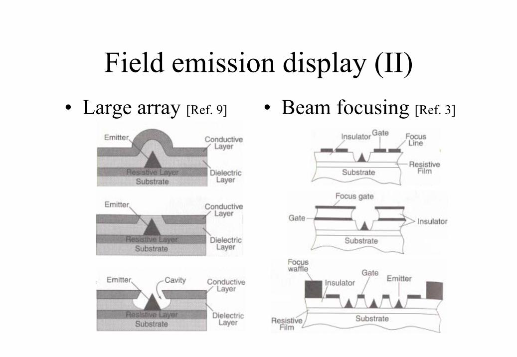
Field emission display (II)• Beam focusing [Ref. 3]• Large array [Ref. 9]
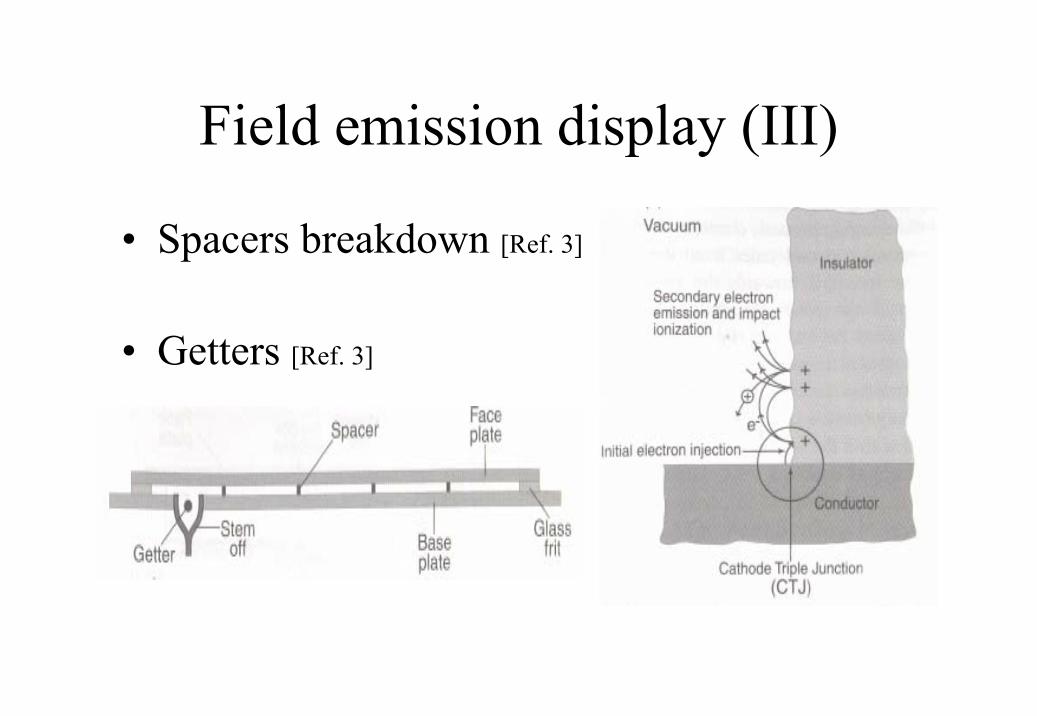
Field emission display (III)
• Spacers breakdown [Ref. 3]
• Getters [Ref. 3]
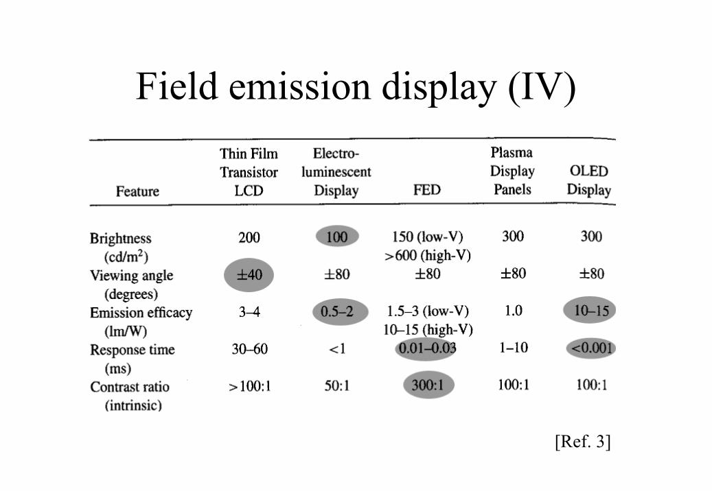
Field emission display (IV)
[Ref. 3]
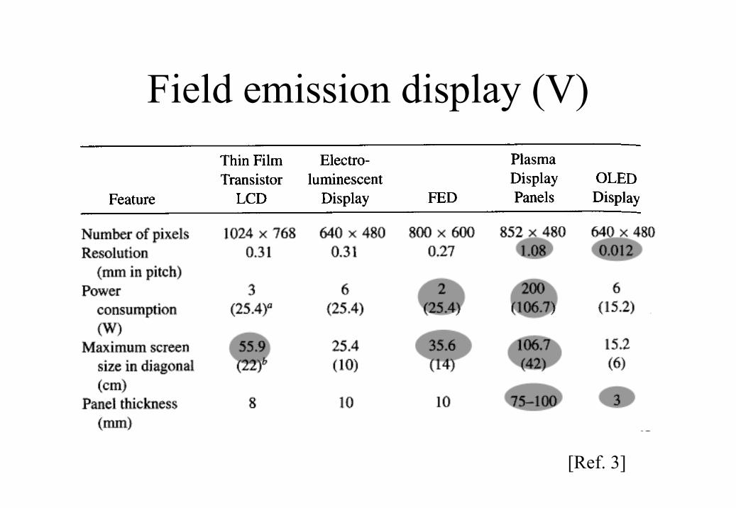
Field emission display (V)
[Ref. 3]
Summary
• An interesting device family• Special design/fabrication considerations• Complementary to conventional solid-state
devices• Important applications
References[1] C. A. Spindt et al., J. Appl. Phys., 47 (1976) 5284[2] F. Charbonnier, Appl. Surf. Sci., 94/95 (1996) 26[3] W. Zhu, Vacuum Microelectronics, John Wiley & Sons, 2001[4] W.Dawson et al., J. Vac. Sci. Tech. B, 11(2),(1993) 518 [5] E. G. Zaidman, Trans. Electron Dev., May 1993, 1009-1016[6] K. L. Jensen, Naval Res. Lab.: Cathode Workshop, 2001[7] http://www.pctechguide.com/07panels.htm[8] T. S. Fahlen, Proc. IVMC, 1999, p. 56[9] T. T. Doan et al., US patent 5229331, 1993