Embed Size (px)
Citation preview
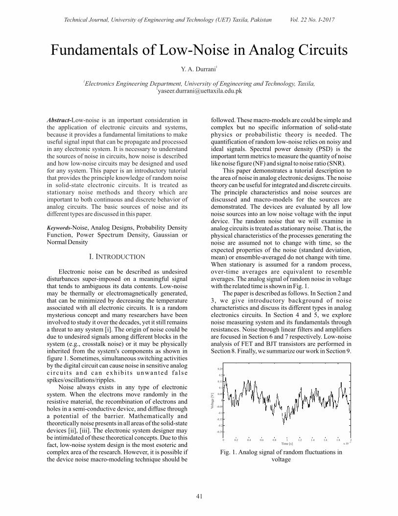
followed. These macro-models are could be simple and complex but no specific information of solid-state physics or probabilistic theory is needed. The quantification of random low-noise relies on noisy and ideal signals. Spectral power density (PSD) is the important term metrics to measure the quantity of noise like noise figure (NF) and signal to noise ratio (SNR). This paper demonstrates a tutorial description to the area of noise in analog electronic designs. The noise theory can be useful for integrated and discrete circuits. The principle characteristics and noise sources are discussed and macro-models for the sources are demonstrated. The devices are evaluated by all low noise sources into an low noise voltage with the input device. The random noise that we will examine in analog circuits is treated as stationary noise. That is, the physical characteristics of the processes generating the noise are assumed not to change with time, so the expected properties of the noise (standard deviation, mean) or ensemble-averaged do not change with time. When stationary is assumed for a random process, over-time averages are equivalent to resemble averages. The analog signal of random noise in voltage with the related time is shown in Fig. 1. The paper is described as follows. In Section 2 and 3, we give introductory background of noise characteristics and discuss its different types in analog electronics circuits. In Section 4 and 5, we explore noise measuring system and its fundamentals through resistances. Noise through linear filters and amplifiers are focused in Section 6 and 7 respectively. Low-noise analysis of FET and BJT transistors are performed in Section 8. Finally, we summarize our work in Section 9.
Fig. 1. Analog signal of random fluctuations in voltage
41
Abstract-Low-noise is an important consideration in the application of electronic circuits and systems, because it provides a fundamental limitations to make useful signal input that can be propagate and processed in any electronic system. It is necessary to understand the sources of noise in circuits, how noise is described and how low-noise circuits may be designed and used for any system. This paper is an introductory tutorial that provides the principle knowledge of random noise in solid-state electronic circuits. It is treated as stationary noise methods and theory which are important to both continuous and discrete behavior of analog circuits. The basic sources of noise and its different types are discussed in this paper.
Keywords-Noise, Analog Designs, Probability Density Function, Power Spectrum Density, Gaussian or Normal Density
I. INTRODUCTION
Electronic noise can be described as undesired disturbances super-imposed on a meaningful signal that tends to ambiguous its data contents. Low-noise may be thermally or electromagnetically generated, that can be minimized by decreasing the temperature associated with all electronic circuits. It is a random mysterious concept and many researchers have been involved to study it over the decades, yet it still remains a threat to any system [i]. The origin of noise could be due to undesired signals among different blocks in the system (e.g., crosstalk noise) or it may be physically inherited from the system's components as shown in figure 1. Sometimes, simultaneous switching activities by the digital circuit can cause noise in sensitive analog c i r c u i t s a n d c a n e x h i b i t s u n w a n t e d f a l s e spikes/oscillations/ripples. Noise always exists in any type of electronic system. When the electrons move randomly in the resistive material, the recombination of electrons and holes in a semi-conductive device, and diffuse through a potential of the barrier. Mathematically and theoretically noise presents in all areas of the solid-state devices [ii], [iii]. The electronic system designer may be intimidated of these theoretical concepts. Due to this fact, low-noise system design is the most esoteric and complex area of the research. However, it is possible if the device noise macro-modeling technique should be
Fundamentals of Low-Noise in Analog Circuits1Y. A. Durrani
1Electronics Engineering Department, University of Engineering and Technology, Taxila, [email protected]
Technical Journal, University of Engineering and Technology (UET) Taxila, Pakistan Vol. 22 No. I-2017
Vol
tage
[V
]
0.25
0.2
0.15
0.1
0.05
0
-0.05
-0.1
-0.15
-0.2
-0.25
Time [s]0 0.2 0.4 0.6 0.8 1 1.2 1.4 1.6 1.8 2
x 10-3
42
also,
(7)
PDFs are useful to describe the amplitude properties of the electrical signal noise. Gaussian or normal density can be included in (8) as:
(8)
The rectangular density in (9) and (10):
(9)
(10)
and using the Rayleigh density in (11):
(11)
The assumption is made that the electrical circuit noise can be parameterized by the Gaussian PDF. It is often a valid approximation for many mathematical benefits. For example, if noise of the Gaussian is the input to a valid linear transfer-function. Then it will be
observed at the output with different variance, than
for the input noise. Generally such case is not used for the noises to describe by other PDFs.
B. Power Spectral Density (PSD) The contents of the low-frequency waveform are the fundamental characteristic which distinguishes a waveform from one another. Generally, a waveform may be characterized either a non-zero (finite) average power with energy infinite signal or as a zero average power (finite energy). The frequency domain expression of a finite-energy waveform can be determined by the Fourier-transform method of the related time domain function. The spectral property of a stationary stochastic signal is determined by evaluating the Fourier-transform of the auto-correlation function. i.e. power spectral density [viii]. PSD is another important descriptor of the noise and normally can be used for the characterization of noise in the frequency domain, regardless of the PDF. We present an operational definition of the PSD that identifies the distribution of “power” in a noise source as compared to the frequency. Let a linear time invariant (LTI) system that is defined by it's impulse-response h(t) whose frequency-response is h(f). If x(t) is the input signal to any system S and if y(t) is the output signal. The system's output may be defined in (12):
(12)
The PSD of the output signal can be express in the form of:
II. CHARACTERIZATIONS OF NOISE
Some important theorems related to continuous and discrete time domain are discussed in this section. Let V(t) is a continuous time zero noise signal and the sequences V(kT) is a sampled of V(t) sampled at time T, 2T,...... The rms value of V(T) can be defined in (1) [iv]:
(1)
and the rms value of the sequence V(kT) is defined in (2):
(2)
where the operator E is the expected value operator.Theorem 1: Assume V(t) is a continuous time zero noise source and then V(kT) is a sample of V(t) at times T, 2T,...... the rms mean value of the continuous It can be defined as:
Theorem 2: Assume V(t) is a continuous time zero noise source and then V(kT) is a sample of V(t) at times T, 2T,...... then the standard deviation of the random
variable V(kT), denoted as satisfies the expression:
Note: There are some parts of the hypothesis of these two theorems that have not been stated such as stationary of the no correlation between samples signal spaced T and the distribution. Part of this theorem appears in [iv].Theorem 3: Assume V(t) is a continuous time zero
noise source with power spectral density N , then the n
noise in rms value can be defined as:
(3)
A. Probability Distribution Function Different statistical and probabilistic techniques were proposed for random low-noise waveforms [v], [vi]. In this paper, the probability density function (PDF) approach is adopted to describe noise [vii]. Let the amplitude statistics of a low-noise voltage waveform n(t) varies with the required time. The PDF
, is defined as: n(t) is the amplitude of the noise sampled at some instant of time t, then in (4):
(4)
The (5) and (6) are the know characteristics/properties of the PDF:
(5)
(6)
Technical Journal, University of Engineering and Technology (UET) Taxila, Pakistan Vol. 22 No. I-2017
43
electron, and is a bandwidth. Transit-time noise is generated when electrons
take time to travel from emitter to the collector and it is comparable to the time period of the amplified signal, that is at different frequencies above the VHF and the beyond, known as transit-time factor that takes place and the noise admittance increases for the transistor.
B. External noise It is generated externally or outside of the system. These are analyzed qualitatively. External noise can be classified such as: Industrial noise is mainly due to industrial noise
in high-voltage wires. These are normally caused by the dis-charge existence in different operations. Some other reasons are ignition of electric motors and switching gears, aircraft, auto-mobiles etc.
Atmospheric noise is a static noise due to some kind of the natural sources of disturbance like thunderstorm, lightning, and the disturbances according to the nature.
Extraterrestrial noise exists on the basis of their originating source. They are sub-classified as solar noise and cosmic noise.
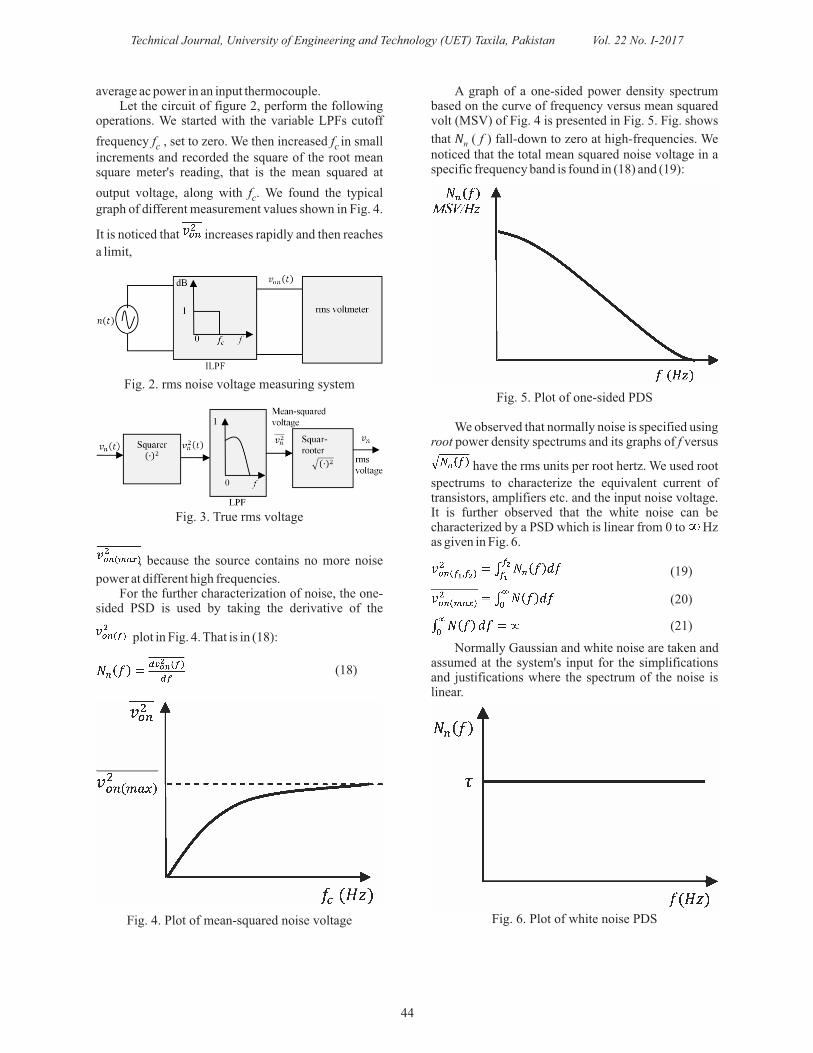
IV. NOISE MEASURING SYSTEM
Let the system of Fig. 2, a noise voltage source is connected to the ideal low pass filter (ILPF), the output is measured with the true rms voltmeter. The true rms voltmeter operation is shown by a system block
diagram in Fig. 2. The input is squared
given to the filter input, then the dc component in
is extracted by a low pass filter (LPF) with a time
constant. At the output of the LPF, , is the mean
squared voltage is square-rooted yielding, in the operation of inverse order of, the rms voltage value of
. A true rms voltmeter must be used for noise measurements due to its only type of ac voltmeter calibrated for random signals, and for all forms of the periodic, deterministic waveforms (triangle waves, sine waves etc.). The operation of true rms meter is performed with active analog circuit component as shown in Fig. 3. A vacuum thermocouple can be used
for true rms meter. In such case, the input v (t), causes on
a temperature rise in a small heater component with
This is directly proportional to P , average power h
consumption in R . . thermocouple is bonded to the h
heater, and it generates an emf, E proportional toO
square-root scale responds to E , giving an indicated O
rms value of v (t). The digital electronic feedback-on
type true rms meters is used to balance the dc power in a reference thermocouple with the input signal's
(13)
where N (f ) is N (f ) y xis the PSD of the output and is the PSD of input signal. As the theorem 3 says in this section, if is a V(t ) continuous time zero noise signal source with single-
side PSD then the rms value of the noise is given in N , v
(14):
(14)
III. NOISE CLASSIFICATION
There are several ways to describe noise and classified its types such as: internal noise and external noise.
A. Internal noise It is generated internally or within the system. It may be behaved qualitatively and may be minimized by the optimized design of the system. Internal noise may have different types:! Thermal noise, Johnson-Nyquist noise or
noise voltage V is generated when the thermal th
energy is due to the free electrons/holes to move in random motion in a resistive component [ix], [x].
(15)
-23 where is (1.38 x 10 ), the Boltzmann's constant
mean-squared voltage in a bandwidth
.normally
Burst noise is due to manufacturing defect and causes by the metallic extrinsic elements in the p-n junction [xi].
Contact noise or flicker noise I is due to contact con
between the two conducting elements when the conductivity to noise in the existence of the dc-current [ix]. Such noise is mathematically modeled by the noise-current-source is parallel with the element. The rms contact noise in the
frequency-band is in (16):
(16)
where I is a dc current, y 1, is a contact noise co-efficient, and x is the contact-noise exponent.
Shot noise is due to discrete arrival times of the electrons flow across the barrier or pn-junction
[ix]. The rms value of the shot-noise current I is sh
given by the Schottky's equation:
(17)
Here I is the dc current source, q is a charge of a
Technical Journal, University of Engineering and Technology (UET) Taxila, Pakistan Vol. 22 No. I-2017
44
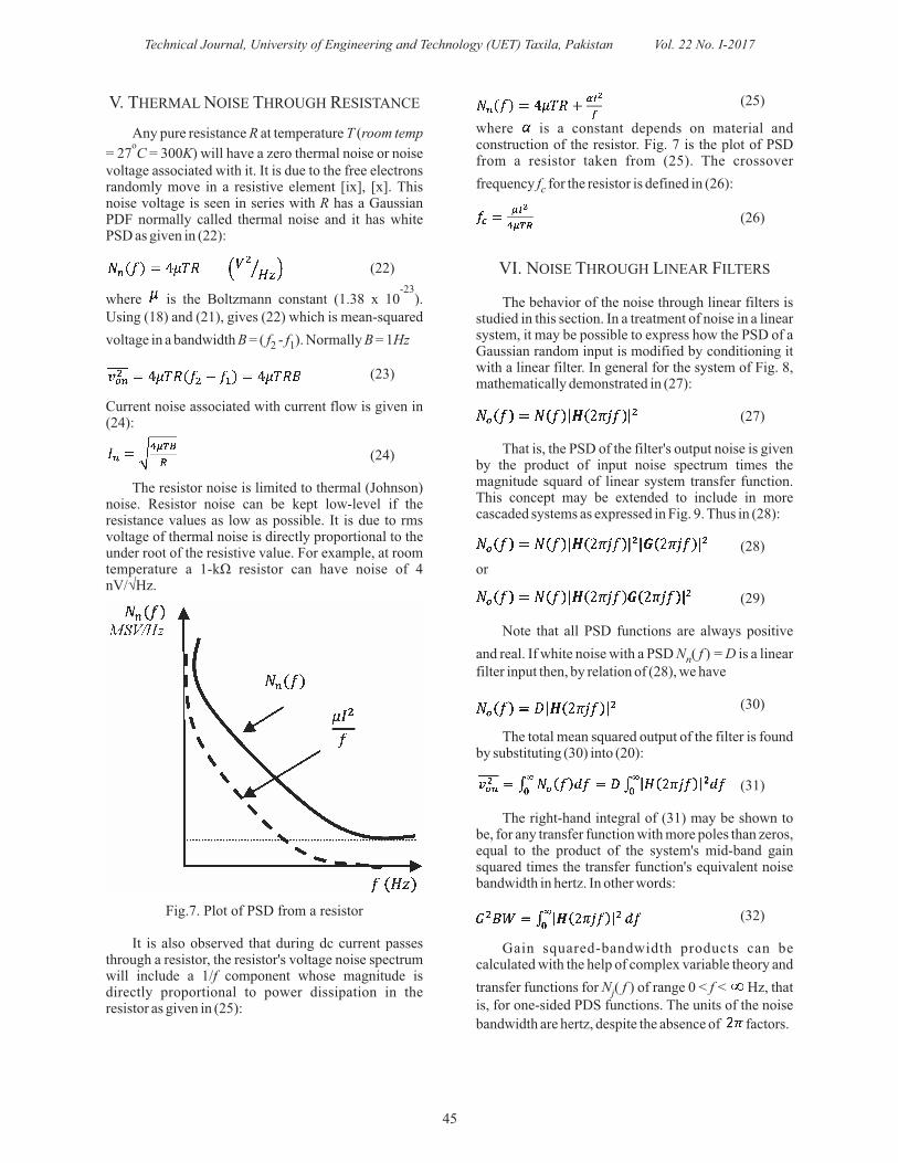
A graph of a one-sided power density spectrum based on the curve of frequency versus mean squared volt (MSV) of Fig. 4 is presented in Fig. 5. Fig. shows
that N ( f ) fall-down to zero at high-frequencies. We n
noticed that the total mean squared noise voltage in a specific frequency band is found in (18) and (19):
Fig. 5. Plot of one-sided PDS
We observed that normally noise is specified using root power density spectrums and its graphs of f versus
have the rms units per root hertz. We used root
spectrums to characterize the equivalent current of transistors, amplifiers etc. and the input noise voltage. It is further observed that the white noise can be characterized by a PSD which is linear from 0 to Hz as given in Fig. 6.
(19)
(20)
(21)
Normally Gaussian and white noise are taken and assumed at the system's input for the simplifications and justifications where the spectrum of the noise is linear.
Fig. 6. Plot of white noise PDS
average ac power in an input thermocouple. Let the circuit of figure 2, perform the following operations. We started with the variable LPFs cutoff
frequency f , set to zero. We then increased f in small c c increments and recorded the square of the root mean square meter's reading, that is the mean squared at
output voltage, along with f . We found the typical cgraph of different measurement values shown in Fig. 4.
It is noticed that increases rapidly and then reaches
a limit,
Fig. 2. rms noise voltage measuring system
Fig. 3. True rms voltage
, because the source contains no more noise
power at different high frequencies. For the further characterization of noise, the one-sided PSD is used by taking the derivative of the
plot in Fig. 4. That is in (18):
(18)
Fig. 4. Plot of mean-squared noise voltage
Technical Journal, University of Engineering and Technology (UET) Taxila, Pakistan Vol. 22 No. I-2017
45
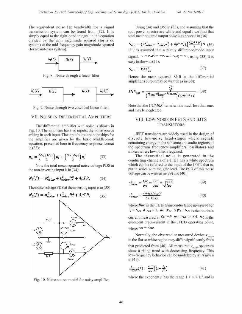
(25)
where is a constant depends on material and construction of the resistor. Fig. 7 is the plot of PSD from a resistor taken from (25). The crossover
frequency f for the resistor is defined in (26):c
(26)
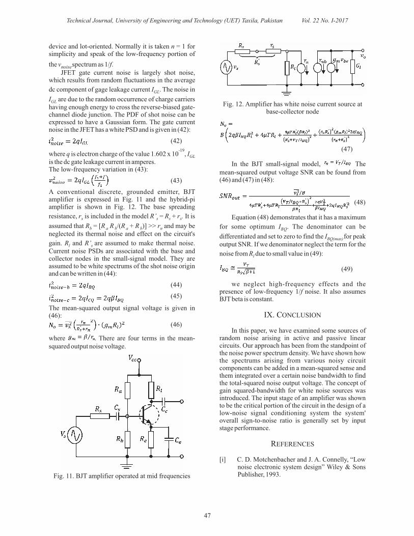
VI. NOISE THROUGH LINEAR FILTERS
The behavior of the noise through linear filters is studied in this section. In a treatment of noise in a linear system, it may be possible to express how the PSD of a Gaussian random input is modified by conditioning it with a linear filter. In general for the system of Fig. 8, mathematically demonstrated in (27):
(27) That is, the PSD of the filter's output noise is given by the product of input noise spectrum times the magnitude squard of linear system transfer function. This concept may be extended to include in more cascaded systems as expressed in Fig. 9. Thus in (28):
(28)
or
(29) Note that all PSD functions are always positive
and real. If white noise with a PSD N ( f ) = D is a linear nfilter input then, by relation of (28), we have
(30)
The total mean squared output of the filter is found by substituting (30) into (20):
(31)
The right-hand integral of (31) may be shown to be, for any transfer function with more poles than zeros, equal to the product of the system's mid-band gain squared times the transfer function's equivalent noise bandwidth in hertz. In other words:
(32)
Gain squared-bandwidth products can be calculated with the help of complex variable theory and
transfer functions for N ( f ) of range 0 < f < Hz, that jis, for one-sided PDS functions. The units of the noise
bandwidth are hertz, despite the absence of factors.
V. THERMAL NOISE THROUGH RESISTANCE
Any pure resistance R at temperature T (room temp o
= 27 C = 300K) will have a zero thermal noise or noise voltage associated with it. It is due to the free electrons randomly move in a resistive element [ix], [x]. This noise voltage is seen in series with R has a Gaussian PDF normally called thermal noise and it has white PSD as given in (22):
(22)
-23where is the Boltzmann constant (1.38 x 10 ). Using (18) and (21), gives (22) which is mean-squared
voltage in a bandwidth B = ( f - f ). Normally B = 1Hz2 1
(23)
Current noise associated with current flow is given in (24):
(24)
The resistor noise is limited to thermal (Johnson) noise. Resistor noise can be kept low-level if the resistance values as low as possible. It is due to rms voltage of thermal noise is directly proportional to the under root of the resistive value. For example, at room temperature a 1-kΩ resistor can have noise of 4 nV/√Hz.
Fig.7. Plot of PSD from a resistor
It is also observed that during dc current passes through a resistor, the resistor's voltage noise spectrum will include a 1/f component whose magnitude is directly proportional to power dissipation in the resistor as given in (25):
Technical Journal, University of Engineering and Technology (UET) Taxila, Pakistan Vol. 22 No. I-2017
46
Using (34) and (35) in (33), and assuming that the root power spectra are white and equal , we find that total mean squared output noise is expressed in (36):
(36)
If it is assumed that a purely difference-mode input
signal, , using (33) it is easy to show in (37):
(37)
Hence the mean squared SNR at the differential amplifier's output may be written as in (38):
(38)
2Note that the 1/CMRR term term is much less than one, and may be neglected.
VIII. LOW-NOISE IN FETS AND BJTS
TRANSISTORS
JFET transistors are widely used in the design of discrete low-noise head-stages where signals containing energy in the subsonic and audio regions of the spectrum frequency amplifiers, oscillators and mixers where low noise is required. The theoretical noise is generated in the conducting channels of a JFET has a white spectrum which can be referred to the input of the JFET, that is, put in series with the gate lead. The PSD of this noise voltage can be written in (39) and (40):
(39)
(40)
where is the FETs transconductance measured for
is the dc-drain
current measured at is the quiescent drain-current at the JFETs operating point,
where
Normally, the observed or measured device vnoise in the flat or white region may differ significantly from
that predicted from (40). All measured v spectrum noise show a rising trend with decreasing frequency. This low-frequency behavior can be modeled by a 1/f given in (41):
(41)
where the exponent n has the range 1 < n < 1.5 and is
The equivalent noise Hz bandwidth for a signal transmission system can be found from (32). It is simply equal to the right-hand integral in the equation divided by the gain magnitude squared (for a dc system) or the mid-frequency gain magnitude squared (for a band-pass system).
Fig. 8. Noise through a linear filter
Fig. 9. Noise through two cascaded linear filters
VII. NOISE IN DIFFERENTIAL AMPLIFIERS
The differential amplifier with noise is shown in Fig. 10. The amplifier has two inputs, the noise source arising in each input. The input/output relationships for the amplifier are given by the basic Middlebrook equation, presented here in frequency response format in (33):
(33)
Now the total mean squared noise voltage PDS at the non-inverting input is in (34):
(34)
The noise voltage PDS at the inverting input is in (35)
(35)
Fig. 10. Noise source model for noisy amplifier
Technical Journal, University of Engineering and Technology (UET) Taxila, Pakistan Vol. 22 No. I-2017
47
Fig. 12. Amplifier has white noise current source at base-collector node
(47)
In the BJT small-signal model, The mean-squared output voltage SNR can be found from (46) and (47) in (48):
(48)
Equation (48) demonstrates that it has a maximum
for some optimum I . The denominator can be BQ
differentiated and set to zero to find the I for peak BQ(max)
output SNR. If we denominator neglect the term for the
noise from R due to small value in (49):l
(49)
we neglect high-frequency effects and the presence of low-frequency 1/f noise. It also assumes BJT beta is constant.
IX. CONCLUSION
In this paper, we have examined some sources of random noise arising in active and passive linear circuits. Our approach has been from the standpoint of the noise power spectrum density. We have shown how the spectrums arising from various noisy circuit components can be added in a mean-squared sense and them integrated over a certain noise bandwidth to find the total-squared noise output voltage. The concept of gain squared-bandwidth for white noise sources was introduced. The input stage of an amplifier was shown to be the critical portion of the circuit in the design of a low-noise signal conditioning system the system' overall sign-to-noise ratio is generally set by input stage performance.
REFERENCES
[i] C. D. Motchenbacher and J. A. Connelly, “Low noise electronic system design” Wiley & Sons Publisher, 1993.
device and lot-oriented. Normally it is taken n = 1 for simplicity and speak of the low-frequency portion of
the v spectrum as 1/f.noise JFET gate current noise is largely shot noise, which results from random fluctuations in the average
dc component of gage leakage current I . The noise in GL
I are due to the random occurrence of charge carriers GL
having enough energy to cross the reverse-biased gate-channel diode junction. The PDF of shot noise can be expressed to have a Gaussian form. The gate current noise in the JFET has a white PSD and is given in (42):
(42)
-19where q is electron charge of the value 1.602 x 10 , IGL
is the dc gate leakage current in amperes.The low-frequency variation in (43):
(43)
A conventional discrete, grounded emitter, BJT amplifier is expressed in Fig. 11 and the hybrid-pi amplifier is shown in Fig. 12. The base spreading
resistance, r is included in the model R’ = R + r . It is x s s x
assumed that R = [R R /(R + R )] >> r and may be b a b a b n
neglected its thermal noise and effect on the circuit's
gain. R and R’ are assumed to make thermal noise. l s
Current noise PSDs are associated with the base and collector nodes in the small-signal model. They are assumed to be white spectrums of the shot noise origin and can be written in (44):
(44)
(45)
The mean-squared output signal voltage is given in (46):
(46)
where . There are four terms in the mean-squared output noise voltage.
Fig. 11. BJT amplifier operated at mid frequencies
Technical Journal, University of Engineering and Technology (UET) Taxila, Pakistan Vol. 22 No. I-2017
48
conference noise physics System 1/f Flucttuat, Vol. 780. pp. 3-12, 2005.
[viii] Y. A. Durrani and T. Riesgo, “Power macro-modelling technique and its application to SoC-based Design” International Journal of Numerical Modeling, Electronic Networks, Devices & Fields, vol. 29, no. 6, 2016.
[ix] P. R. Graay and R. G. Meyerr, “Analysis and design of analog integrated circuits,” Wiley& Sons Publisher, 1993.
[x] W. Yu, and B. H. Leung,“Noise Analysis for S a m p l i n g M i x e r s U s i n g S t o c h a s t i c DifferentialEquations,”IEEE Transactions on Circuits and Systems- II: Analog and Digital Signal Processing, Vol. 46(6), 1999.
[xi] V. Vasudevan, “A Time-domain technique for computation of noise-spectral densityin linear and nonlinear time-varying circuits,”IEEE Transaction on Circuits and SystemsI, vol. 51(2), 2004.
[ii] A. M. Abo and P. R. Gray, “A 1.5-V 10-bit 14.3-MS/s CMOS pipeline analog-to-digital converter,” IEEE Journal of Solid-State Circuits, vol. 34, pp. 599–606, May 1999.
[iii] R. Gregorian and C. Temas, “Analog MOS integrate circuits for signal processing”, JohnWiley &Sons Publisher,1986.
[iv] B. Razavi, “Design of analog CMOS integrated circuits”, McGraw-Hill publisher, Inc. 2001.
[v] H. Ott, “Noise reduction techniques in electronic systems”, 2nd Ed.,John Wiley& Sons Publisher,1988.
[vi] G. Al Sammane, M. Zaki, and S. Tahar, “A symbolic methodology for the verificationof analog and mixed signal designs”, IEEE Transaction on Design Automation and Test in Europe, pp. 249-254, 2007.
[vii] P. Papeer, M. J. Den, and O. Marinnov, “Noise in advance electronic devices & circuits,” in the Proceedings of A.I .P Interternational
Technical Journal, University of Engineering and Technology (UET) Taxila, Pakistan Vol. 22 No. I-2017


![[PPT] Noise and Matching in CMOS (Analog) Circuits](https://img.pdfslide.net/doc/110x75/55cf932b550346f57b9c555d/ppt-noise-and-matching-in-cmos-analog-circuits.jpg)