Embed Size (px)
Citation preview

Fundamentals of positron annihilation spectroscopy Fundamentals of positron annihilation spectroscopy p p pyp p pyand and its application in semiconductorsits application in semiconductors
Reinhard Krause-Rehberg
i i i i GMartin-Luther-University Halle-Wittenberg, Germany

Point defects determine properties of materialsPoint defects determine properties of materials
Galliumphosphide1 cm
• Point defects determine electronic and optical properties
• electric conductivity strongly• electric conductivity strongly influenced
without vacancies with 0 001% vacancieswithout vacancies with 0.001% vacanciestransparent opaque
1 vacancy in 100000 atoms
• Point defects are generated by irradiation (e.g. cosmic rays), by plastic deformation or by diffusion, …
• Metals in high radiation environment - formation of voids - embrittlement
• P i f i d h i d f b k• Properties of vacancies and other point defects must be known
• Analytical tools are needed to characterize point defects
• Positron Annihilation is a unique tool for nano-sized open-volume defectsq p

ContentContent
1. Positron production• isotope sources (22-Na, 64-Cu, 58-Co)• pair production (Bremsstrahlung from accelerators, reactor-based positron sources)
2. Methods of Positron Annihilation Spectroscopy• Positron lifetime spectroscopy• Angular correlation of annihilation radiation - ACAR• Doppler broadening spectroscopy• Age-momentum correlation (AMOC)
3. Possible setups• Sandwich geometry with isotope sources• Gamma-induced Positron Spectroscopy (GiPS at EPOS)• Positron beam setups (continuous and bunched beams, focused systems)
l d di d i f ili i4. Large-scale user-dedicated positron facilities5. Defect spectroscopy by Positrons
• Trapping model• Determination of trapping coefficient
6. Peculiarities of Positron Annihilation in semiconductors7. Defect studies in semiconductors – 11 Examples8. Conclusions9. Literature

1. Positron generation: isotope sources 1. Positron generation: isotope sources
Positrons are obtained for laboratory setups usually by the β+ decay of isotopes
22 64 8 68• Most popular isotopes: 22Na, 64Cu, 58Co and 68Ge
• 22Na has many advantages: long half life (2.6 a); short biological half life (3 d); relatively cheap; effective (>90% in β decay); easy to handle in water solution as 22NaCl or 22Na COeffective (>90% in β decay); easy to handle in water solution as NaCl or Na2CO3
• β+ decay: 22Na → 22Ne + β+ + νe + γ(1.27MeV)
• 1 27 MeV γ appears almost simultaneously with positron can be used as start event for lifetime• 1.27 MeV γ appears almost simultaneously with positron - can be used as start event for lifetime spectroscopy
Decay scheme of 22Na positron energy distribution4

1. Positron generation: pair production1. Positron generation: pair production
For high-flux positron facilities: Positrons are obtained by pair production
• pair production using bremsstrahlung of a decelerated beam of MeV-electrons of a LINAC onto a t t (EPOS i R d f G KEK i T k b J AIST i T k b J ANL itarget (EPOS in Rossendorf, Germany; KEK in Tsukuba, Japan; AIST in Tsukuba, Japan; ANL in Argonne, USA; …)
• Gamma background from fission reactions in a reactor can be used: Reactor Centre at Delft University, The Netherlands
• Gamma generation from nuclear reaction: 113Cd(n,γ)114Cd → three γ rays and pair production; continuous positron beam; ≈ 5x10⁸ e+/s (Research Reactor in Garching Germany)continuous positron beam; ≈ 5x10 e /s (Research Reactor in Garching, Germany)
5NEPOMUC Source in Garching
The electron to gamma to positron converter at EPOS (Rossendorf)

22Na2. Methods of Positron Annihilation Spectroscopy2. Methods of Positron Annihilation Spectroscopy
• positron wave-function can be localized in the attractive potential of
Na
a defect
• annihilation parameters change in the localized state
• e.g. positron lifetime increases in a vacancyvacancy
• lifetime is measured as time difference between appearance of 1.27 (start) and 0.51 MeV (stop) quanta
• defect identification and quantification possible

2. Methods of Positron Annihilation Spectroscopy: 2. Methods of Positron Annihilation Spectroscopy: Positron Lifetime SpectroscopyPositron Lifetime Spectroscopy -- PALSPALSPositron Lifetime Spectroscopy Positron Lifetime Spectroscopy PALSPALS
• positron lifetime is measured in a 22Na pos o e e s e su edlaboratory setup as the time difference between the 1.27 MeV and the annihilation 0 511 MeV gamma q anta0.511 MeV gamma quanta
• in a pulsed positron beam: time difference between 0.511 quantum and machine pulse q pfrom timing system (e.g. PLEPS system at NEPOMUC)
7

Isotope source: Maximum source strength
• in case of non-periodic sources (i t )(isotope sources):
• positron source activity must be adopted to maximum lifetime to be adopted to a u et e to bemeasured
• mean time between 2 positron must be
fetim
e
much larger than positron lifetime
• we performed MC simulations to d t i thi l ti
Lif
determine this correlation
• to have reasonable background in metals/semiconductors (t < 0.5 ns):
S. Thraenert, E.M. Hassan, R. Krause-Rehberg, NIM B248 (2006) 336.
metals/semiconductors (t 0.5 ns): source should be ≤ 25 µCi
• for porosimetry (e.g. pore diameter = 10 nm) source should have ≤ 5 µCi

The conventional Positron Lifetime Measurement
- Positron lifetime is measured as time difference between 1.27 MeV quantum (β+ decay) and 0 11 ( ihil i )0.511 MeV quanta (annihilation process)
- PM…photomultiplier; SCA…single channel analyzer (constant-fraction type); TAC…time to amplitude converter; MCA… multi channel analyzer
9

Digital lifetime measurement
• much simpler setuplik d l h l ill• like a dual-channel oscilloscope
• timing very accurate (10-6)• pulse-shape discrimination (suppress
“bad pulses”)bad pulses )• each detector for start & stop (double
statistics)
2 acqiris digitizer DP211 (1 GHz bandwidth / 4GS/s)
10

Screenshot of two digitized anode pulses
time difference = 2.65471 samples = 663.67 ps
11

Positron lifetime spectroscopy
106
As–grown Cz SiPlastically deformed Si
• positron lifetime spectra consist of exponential decay components
105
Plastically deformed Si • positron trapping in open-volume defects leads to long-lived components
• longer lifetime due to lower electron density
104
τ2 = 320 ps
nts
longer lifetime due to lower electron density
• analysis by non-linear fitting: lifetimes ti and intensities Ii
(divacancies)
10
τ = 218 ps
τ3 = 520 ps
Cou
(vacancy l t )
103τb = 218 ps clusters)
(bulk)
0 1 2 3 4 5
Time [ns]Time [ns]
Martin-Luther-Universität Halle12

Typical Lifetimes
Sources of PositronSources of Positron
Positron Positronium

2. Methods of Positron Annihilation Spectroscopy: 2. Methods of Positron Annihilation Spectroscopy: Angular Correlation of Annihilation RadiationAngular Correlation of Annihilation Radiation -- ACARACARAngular Correlation of Annihilation Radiation Angular Correlation of Annihilation Radiation ACARACAR
14

2-D Angular Correlation of Annihilation Radiation
15

2D-ACAR of defect-free GaAs
(Tanigawa et al , 1995) 3D Fermi surface can be reconstructed from measurements in(Tanigawa et al., 1995) 3D-Fermi surface can be reconstructed from measurements in several directions of a single crystal 16

2D-ACAR of Copper
Theory Experiment
g [1
00]
p zal
ong
Fermi surfaceFermi surface of copper
(Berko, 1979)py along [010]
17

2. Methods of Positron Annihilation Spectroscopy: 2. Methods of Positron Annihilation Spectroscopy: Doppler Broadening Spectroscopy Doppler Broadening Spectroscopy -- DBSDBSpp g p pypp g p py
18

Measurement of Doppler Broadening
- electron momentum in propagation direction of 511 keV γ-ray leads to Doppler broadening p p g γ y pp gof annihilation line
- can be detected by conventional energy-dispersive Ge detectors and standard electronics
19

Effect of Doppler Broadening
• width of 85Sr line corresponds to the energy resolution of Ge detector
• 511 keV annihilation line distinctly broader due to momentum of annihilating gelectrons
• defect-rich sample show more narrow curveso e ow cu ves
• Effect due to enhanced annihilation with valence electrons in open-volumeelectrons in open volume defects (e.g. in vacancies)
• they have smaller momenta: smaller Dopplermomenta: smaller Doppler shift
20

Line Shape Parameters
S parameter (shape):
S = AS/A0
W parameter (wing):
W = AW/A0
• W parameter mainly determined by yannihilations of core electrons (chemical information)
• however: almost in background
f l S W• very useful S-versus-W plot 21

S versus W plot
• Doppler results after ion implantation in Si obtained by a slow-positron beam• S and W values were normalized to the respective bulk values• the S-W-plot allows to identify the annihilation sitethe S W plot allows to identify the annihilation site
S. Eichler et al., Phys. Rev. B 56 (1997) 1393
22
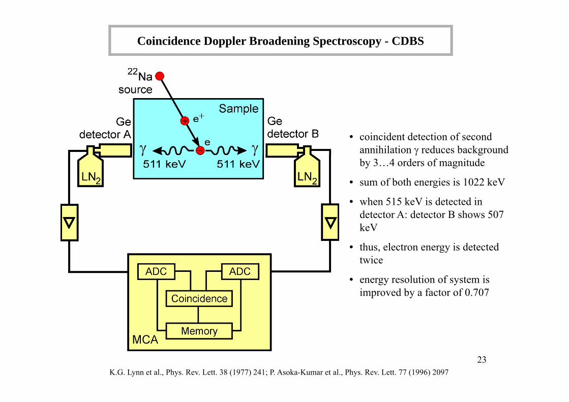
Coincidence Doppler Broadening Spectroscopy - CDBS
• coincident detection of second annihilation γ reduces background γ gby 3…4 orders of magnitude
• sum of both energies is 1022 keV
• when 515 keV is detected in• when 515 keV is detected in detector A: detector B shows 507 keV
• thus electron energy is detected• thus, electron energy is detected twice
• energy resolution of system is improved by a factor of 0 707improved by a factor of 0.707
23K.G. Lynn et al., Phys. Rev. Lett. 38 (1977) 241; P. Asoka-Kumar et al., Phys. Rev. Lett. 77 (1996) 2097

CBDS Spectra: the effect of coincident detection
100
10-1
ty
GaAs:Znsingle Ge detector DBS
10-3
10-2
e in
tens
it
Conicidence with NaI
10-4
10
Rel
ativ
Coincidence with second Ge detector
500 505 510 515 520 525
10-5Ge detector
γ-ray energy [keV]
Eγ1+Eγ2= 2 m0 c2 =1022 keV24

CDBS spectra in GaAs
• Chemical sensitivity due to electrons at high momentum (core electrons)• a single impurity atom aside a vacancy is detectable• examples: VGa-TeAs in GaAs:Te
J. Gebauer et al., Phys. Rev. B 60 (1999) 1464 25

2. Methods of Positron Annihilation Spectroscopy: 2. Methods of Positron Annihilation Spectroscopy: AgeAge--Momentum Correlation Momentum Correlation -- AMOCAMOC
• lifetime and Doppler shift are measured for the samepositron in triple coincidence
• electron momentum is plotted as function of positron age
• interesting application for g ppsoft matter research
• count rate extremely low (< 10 s-1)( )
• better to be performed at bunched intense lifetime beamsbeams
• example was measured in Dec08 in Rossendorf
26
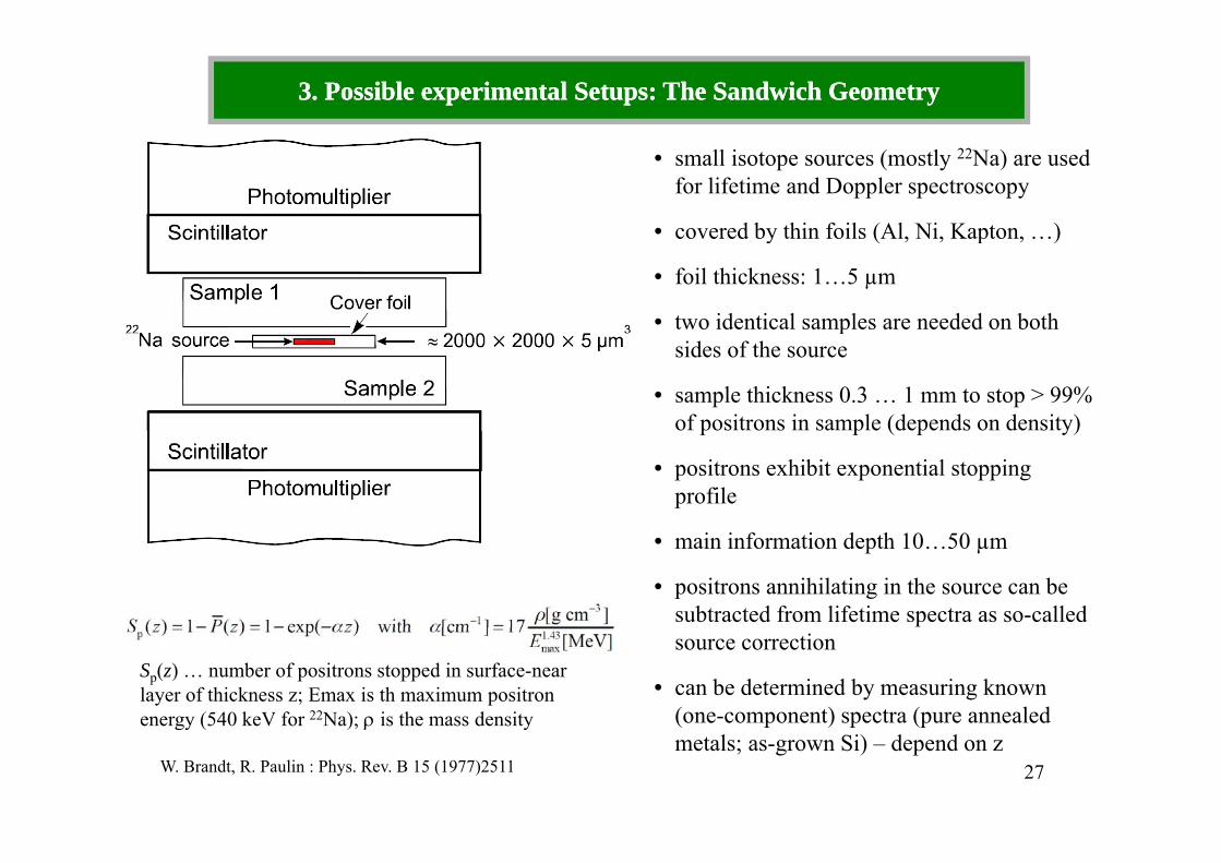
3. Possible experimental Setups: The Sandwich Geometry3. Possible experimental Setups: The Sandwich Geometry
• small isotope sources (mostly 22Na) are used for lifetime and Doppler spectroscopy
• covered by thin foils (Al Ni Kapton )covered by thin foils (Al, Ni, Kapton, …)
• foil thickness: 1…5 µm
• two identical samples are needed on both psides of the source
• sample thickness 0.3 … 1 mm to stop > 99% of positrons in sample (depends on density)p p ( p y)
• positrons exhibit exponential stopping profile
• main information depth 10…50 µm
• positrons annihilating in the source can be subtracted from lifetime spectra as so-called source correction
• can be determined by measuring known (one-component) spectra (pure annealed
Sp(z) … number of positrons stopped in surface-near layer of thickness z; Emax is th maximum positron energy (540 keV for 22Na); ρ is the mass density
27
( p ) p (pmetals; as-grown Si) – depend on z
energy (540 keV for Na); ρ is the mass density
W. Brandt, R. Paulin : Phys. Rev. B 15 (1977)2511

3. Possible Experimental Setups: Gamma3. Possible Experimental Setups: Gamma--induced Positron Spectroscopy induced Positron Spectroscopy -- GiPSGiPS
• positrons are generated inside the whole volume of sample by bremsstrahlung of MeV electron beam
• information from the whole sample (several cm thickness)
• ideal for non-destructive testing of large components or e.g. liquids; biological samples
• with usual Linacs (< 1kHz): many gammas in a few bunches; not suitable for lifetime spectroscopy
l t ti ti d P k/B k d ti f b t 1 1• very low statistics and poor Peak/Background ratio of about 1:1
• improvement: superconducting Linac with high repetition rate (26 MHz at ELBE)
28F.A. Selim et al., Intern. Centre for Diffract. Data 2003, Advances in X-ray analysis, Vol. 46

Gamma-induced Positron Spectroscopy (GiPS) at ELBE (in Rossendorf)
• ELBE provides a pulsed electron beam with extremely sharp bunches (5 ps bunch length; up to 40 MeV; 1 mA average current)
• among 5 experiments at ELBE: a bremsstrahlung gamma source existsamong 5 experiments at ELBE: a bremsstrahlung gamma source exists
• provides a collimated und pulsed gamma beam with high intensity
• time structure suitable for lifetime spectroscopyp py
29

Coincident Detector System of GiPS at ELBE
• detector system was modified to have 2 AMOC and 1 CDBS spectrometer at the same time
• count rate can be adapted by electron current of primary ELBE beam
• lifetime measurement as time difference of BaF2 detector signal and ELBE machine pulse
30AMOC: Age-Momentum CorrelationCDBS : Concidence Doppler-Broadening Spectroscopy

First GiPS spectra at ELBE
• lifetime spectrum is obtained in coincidence with Ge detector to reduce background
• good spectra quality obtained:• Count rate for one AMOC spectrum = 160 /s• Time resolution = 210 ps• BG / Peak = 1 7 x 10⁻⁵• BG / Peak = 1.7 x 10• AMOC and CDBS is measured at the same
time:
AMOC spectrum of Fe
31
CDBS spectrum of Fe

3. Possible Experimental Setups: Positron beams3. Possible Experimental Setups: Positron beamsVariable Energy Positron Annihilation Spectroscopy (VEPAS)Variable Energy Positron Annihilation Spectroscopy (VEPAS)
• often: only thin near-surface layers are of interest (surface modification; ion-implantation; epitaxy …)
i t β b d it• isotope β sources: broad positron emission spectrum up to 540 keV (22Na)
• deep implantation into solids
Mean (maximum) depth in:
• Si: 50µm (770µm)
• GaAs: 22µm (330µm)
• PbS: 15µm (220µm)
• “moderation” necessaryy
• provides monoenergetic positrons
• can be guided as slow-positron beam to the sample

Moderation of Positrons
moderation efficiency: ≈10-4 33

The Positron Beam System at Halle University
• typical continuous laboratory positron beam
• defect-depth profiles can be measured by variation of acceleration voltage
• ExB filter can be replaced by a bended tube for simplicity
• no lifetime spectroscopy possible
34

Implantation Profiles of monoenergetic Positrons
d h l i i f i f- depth resolution is function of implantation depth
- exact implantation profiles areexact implantation profiles are obtained by Monte-Carlo simulations
z = f (E,ρ) z0 = const. m = 2( kh 1961)(Makhov, 1961)
35
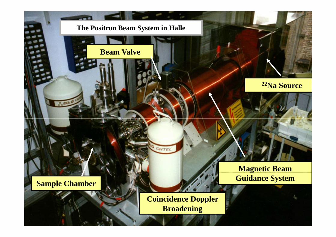
The Positron Beam System in Halle
Beam Valve
22Na Source
Magnetic Beam
Sample Chamber
Coincidence Doppler
gGuidance System
Coincidence Doppler Broadening

Positron Lifetime at a Beam System using Isotope Sources
• a continuous beam can be bunched• a continuous beam can be bunched
• positron lifetime spectroscopy possible
Martin-Luther-Universität Halle
• e.g. PLEPS system at Garching

4. Large4. Large--scale userscale user--dedicated Positron Facilitiesdedicated Positron Facilities
List not complete:
• NEPOMUC at FRM-II in Garching (Munich) / Germany
• reactor-based; 5 beamlines: Lifetime; CDBS; PAES; Microscope (planned – see below); 1 free port for user experiments
• 5 108 +/ hi h t l it fl f• 5x10⁸ e+/s – highest slow-positron flux so far
• Argonne Project APosS / USA
• Linac 15 5 MeV 0 1 mA 60 HzLinac, 15.5 MeV, 0.1 mA, 60 Hz
• First positrons detected – up to 3x10⁹ e+/s expected
• Helsinki Pulsed Positron Beam at HUT / Finland
• Slow-positron lifetime beam based on isotope source
• SOPHI Project in Saclay / France – Mini LINAC for Gravity Experiment with Anti-H
• Tabletop commercial accelerator: 6 MeV, 300 Hz, 0.2 mA; 10 kW
• Under construction (solid Ne moderator possible)
• Aim 108 e+/s38

• Positron Microbeam for Transmission Positron Microscope at KEK (Japanese Collaboration)• Positron Microbeam for Transmission Positron Microscope at KEK (Japanese Collaboration)
• 60 µm diameter after remoderation
• Amazing results for Ni transmission moderator (up to 20% efficiency)Amazing results for Ni transmission moderator (up to 20% efficiency)
• Positron Beam at IHEP Beijing / China
• Many promising activities: lifetime, AMOC, CDBSy p g , ,
• Isotope and LINAC-based bunched slow positron beams
• Positron Probe Micro Analyzer (PPMA) at AIST (Tsukuba) /Japan
• 100 µm beam (10µm expected); lifetime; 200…300 s/ pixel; 200ps FMHM expected
• Australian Positron beam Facility
• 2 beam lines: materials science & atomic/bio/molecular
• AMO beam line: Pulsed; rare gas moderator; 25 meV energy resolution expected
• Materials beam line under construction; aim: bunched 200ps FWHM; 107 e+/s
39

• EPOS: ELBE Positron Source @ Research Centre Dresden Rossendorf / Germany
o 40 MeV, 1 mA, 26 MHz repetition time in cw mode; lifetime, CDBS and AMOC with slow e+o 40 MeV, 1 mA, 26 MHz repetition time in cw mode; lifetime, CDBS and AMOC with slow e
o Retain original time structure for simplicity and best time resolution
o Gamma-induced Positron Spectroscopy for bulky samples
40

Scheme of the Munich Microscope
• d d i l i ll
Scheme of the Munich Microscope
• moderated positrons are electrostatically focused, choppered and bunched
• second moderator stage allows focus down to about 2 µmdown to about 2 µm
• positron penetration energy adjustable for depth information
• t d b 22N• operated by 22Na source• instrument shall be adopted to the
NEPOMUC source at FRM-II in the near futurenear future
41

Scanning Positron Microscope in Munich
42

Scanning Positron Microscope in Munich
defects near a crack in fatigued Cu
τ (ps)Semiconductor test structure
τ (ps)
Nature 412 (2001)764Phys. Rev. Lett. 87, 067402 43

Micro-hardness indentation in GaAs
• Comparison of scanning electron microscopy (SEM), cathodoluminescence (CL) and Munich Positron Scanning Microscope
• problem here at the moment: intensity
SEMCL
• microscope will be transferred to NEPOMUC source at Garching Research Reactor
SEMCLPositrons
Martin-Luther-Universität Halle(Krause-Rehberg et al., 2002)

5. Defect Spectroscopy using Positrons5. Defect Spectroscopy using Positrons
• Positrons are trapped by lattice defects
• trapping can be limited by
th diff i t th d f t− the diffusion to the defect
− or by the trapping process itself, i.e. by the energy release during transition into bound state
• trapping rate κ is proportional to defect density C
45

Localization of the positron wave-function: GaAs bulk vs. VGa
GaAs - bulk GaAs - V Gae+ probability
densityec
tion
0.05
001]
dire
As
0
[0 As
Ga
[110] direction [110] direction
τbulk= 230 ps τ = 260 ps
1/τ=λ~∫dr n n γ(n(r)) τ…lifetime
τbulk 230 ps τvacancy= 260 ps
1/τ=λ~∫dr nelectron npositron γ(n(r)) λ…annihilation rate

Trapping Model: Positron Trapping in a Single Defect Type
solution: decay spectrumy p
47

Complex Example: Positron Trapping in a Dislocation
the dislocation line (shallow trap) acts as a “funnel” for the trapping in deep trapspp g p p
b ... bulk
v ... vacancy
t ... deep trap
st shallow trapst ... shallow trap
48

Determination of absolute Defect Densities
• the trapping coefficient µ must be determined by an independent method
1011
10-8 10-7 10-6 10-5 10-4 10-3 10-2
V−
s−1]
• positron trapping may be strongly temperature dependent: µ = f (T)109
1010Sensitivity range
V
V2−V0 V+
ping
rate
[s
temperature-dependent: µ = f (T)
108
10
Trap
p
d f t i Si (1015 1)
V−
τd
lifet
ime
defect in Si300K µ (1015 s-1)
V- 1
V2 2V
V2− V0 V+
e po
sitro
n V2- 2
V0 0.5
V+ < 0 1
τb
Aver
age V+ < 0.1
dislocation 1 cm2s-1
l t10-8 10-7 10-6 10-5 10-4 10-3 10-2b
Vacancy concentration
vacancy cluster n ·µ1V
49

• Defects with open-volume
What defects can be studied in crystalline solids?
Defects with open volume- vacancies - vacancy clusters / voids- dislocations
360
380
400
ps]
Vacancy clusters
- grain boundaries (for grains < 1µm)- surface (outer and inner)
• Defects without open-volume 300
320
340
360
life
time
[p
- Precipitates- negatively charged defects /shallow
traps (e.g. ionized acceptors in semiconductors) 220
240
260
280theoretical calculation by
Saito, Oshiyama (1996) Hakala et al. (1997) Puska, Corbel (1988)Po
sitro
n
)
0 1 2 3 4 5 6 7 8 9 10200
Vacancy cluster sizePositron trapping in / at Precipitates
Martin-Luther-Universität Halle

6. Pecularities of Positron Annihilation in Semiconductors6. Pecularities of Positron Annihilation in Semiconductors
Positron trapping at vacancies … at shallow traps
• deep, localized states due to missing ion core, no detrapping
• lifetime > τb lk Doppler broadening decreases
• shallow, delocalized state
• thermal detrapping at 300 K lifetime > τbulk , Doppler broadening decreases
lifetime = τbulktrapping independent of temperature
trapping increases withdecreasing temperatureof temperature decreasing temperature
M.J. Puska, Phys. Rev. B 41, 9980 (1990)

Positron Trapping Potential
- Attractive potential mainly due to missing ion (repelling core is absent)
- in semiconductors: additional Coulomb tails (rather extended)
i i b i i i ( i ll d)- no positron trapping by positive vacancies (positrons are repelled)
- temperature dependence expected 52

Different sensitivity for differently charged vacancies
• defects in semiconductors can be charged
• large influence on trapping behavior especially at low temperatures
• trapping coefficient is function of T
• positive vacancies repel p ppositrons
M.J. Puska, R.M. Nieminen: Rev. Mod. Phys. 66 (1991) 841

Negative vacancies show temperature-dependent positron trappingpositron trapping
• temperature dependence of positron trapping is rather complex
• low temperature: κ~T-0.5 due to diffusion limitation in Rydberg stateslimitation in Rydberg states
• higher T: stronger temperature dependence due to thermal detrapping from Rydberg state
positron trapping in negatively charged Gavacancies in SI-GaAs
Le Berre et al., 1995

Fermi-level Dependence of Charge State
• charge state of defect depend on position of Fermi level
Fermi level
Mascher P., et al.: Phys. Rev. B 40 (1989) 11764
• in the above example: mono- and di-vacancies carry a single negative charge while the vacancy-phosphorus pair and the A center (vacancy-oxygen pair) remain neutral
• Fermi level can be shifted by
− temperature change
− doping (impurity in-diffusion)
− defect generation (e.g. by irradiation)
− light illumination (wavelength dependence)

Negative ions act as shallow positron traps
• at low T: negatively charged defects without open volume may trap positrons
“ h ll ” d t ll it bi di• “shallow” due to small positron binding energy
• annihilation parameters close to bulk parameters
• thermally stimulated detrapping δ can be described by:
κ ... trapping rate of shallow trapsρst ... density of shallow traps
Examples:
• negatively charged point defects without open volume
M. Manninen, R.M. Nieminen: Appl Phys A 26 (1981) 93
Est ... positron binding energy to shallow traps• ionized acceptors
• negatively charged antisite defects
• vacancy defects with very small open volume: the A center in Appl. Phys. A 26 (1981) 93y y pSi (Vac-O-complex)

Trapping model of shallow Positron Traps
• positron trapping model gets morepositron trapping model gets more complex
• however: trapping at shallow traps can usually be avoided at high y gtemperatures due to small positron binding energy
• shallow traps can only be seen in p ylifetime spectra when open-volume defects are present (e.g. vacancies)
• this is because positron defect lifetime is almost equal to bulk value
shallow trap vacancy

Effect of shallow positron traps in lifetime spectra
• temperature dependence is characterized by competing trapping by vacancies andcompeting trapping by vacancies and shallow traps
• in GaAs:Si we observe VGa-SiGa complexes at high temperatures g e pe u es
• and SiGa- donors at low T in addition
(shallow traps) at low temperatures
• when vacancies and shallow traps appear at• when vacancies and shallow traps appear at the same time, lifetime spectra decomposition becomes very difficult or rather impossible
trapping by vacanciesl d ( i )
competing trapping centres at low Tshallow positron traps (SiGa
-)
J. Gebauer et al. 1997
at elevated temperatures (VGa-SiGa)
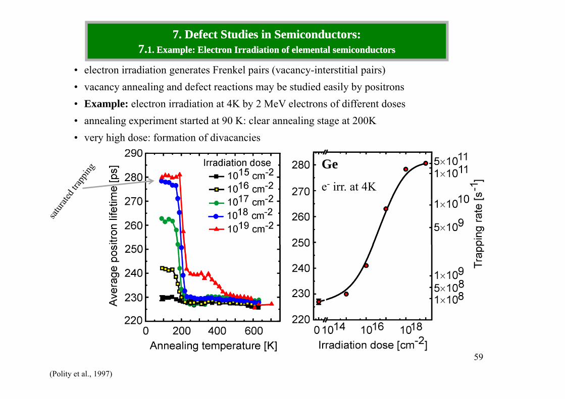
7. Defect Studies in Semiconductors: 7. Defect Studies in Semiconductors: 7.7.1. Example: Electron Irradiation of elemental semiconductors1. Example: Electron Irradiation of elemental semiconductors
• electron irradiation generates Frenkel pairs (vacancy-interstitial pairs)• vacancy annealing and defect reactions may be studied easily by positrons• Example: electron irradiation at 4K by 2 MeV electrons of different dosesp y• annealing experiment started at 90 K: clear annealing stage at 200K• very high dose: formation of divacancies
Ge
e- irr. at 4K
(Polity et al., 1997)
59

Electron irradiation of Si
• low-temperature electron irradiation was performed at 4K (Ee-= 2 MeV)
• annealing stage of monovacancies at about 170 K
• moving VSi partly form divacancies
• divacancies anneal at about 550…650 Kdivacancies anneal at about 550…650 K
Polit et al Ph s Re B 58 (1998) 10363Polity et al., Phys. Rev. B 58 (1998) 10363

7.2. GaAs: annealing under defined As-partial pressure
• two-zone-furnace: Control of sample temperature and As partial pressure allows to navigate freely in phase diagram (existencenavigate freely in phase diagram (existence area of compound)
Tsample: 1100° C TAs: determines As-partial pressure
H. Wenzl et al., J. Cryst. Growth 109, 191 (1991).

GaAs: Annealing under defined As pressure
GaAs:Si
1018
[T ] i -3
GaAs:Te
)
SiGa-VGa TeAs-VGaat
ion
(cm
-3)
1017
[Te] in cm-3
6x10¹⁸ 250
245
K (p
s)
tratio
n (c
m-3)
1017
cy c
once
ntra 10
17
2x10¹⁸
235
240
τ av a
t 55
0 K
ncy
conc
ent
0 01 0 1 1 10
Linear fit
Vac
anc
1016
9x10¹⁶
4x10¹⁷
231
τ
Vaca
n
0,01 0,1 1 10Arsenic pressure (bar) 0,1 1 10Arsenic pressure (bar)
Thermodynamic reaction:1/4 As4
gas ↔ AsAs + VGa
J. Gebauer et al.,Physica B 273-274, 705 (1999)
Fit: [VGa-Dopant] ~ pAsn
n = 1/4
1/4 As4 ↔ AsAs VGa
Mass action law:
[VG ] = KVG × pA1/4 n 1/4[VGa] KVG × pAs

Comparison of doped and undoped GaAs
Thermodynamic reaction:yAsAs ↔ VAs + 1/4As4
gas
Mass action law:
[VAs] = KVAs × pAs-1/4
Fit: [V-complex] ~ pAsnFit: [V complex] pAs
n = -1/4
undoped GaAs: As vacancy
Bondarenko et al., 2003

7.3. Vacancy clusters in semiconductors
• vacancy clusters were observed after neutron irradiation, ion implantation and plastic deformation
• due to large open volume (low electron density) -> positron lifetime increases distinctly
• example: high-temperature plastically deformed GGe
• lifetime: τvoid = 525 ps
• reason for void formation: jog dragging mechanism
• trapping rate of voids disappears during annealing experiment
Krause-Rehberg et al., 1993

Theoretical calculation of vacancy clusters in Si
• there are cluster configurations with a large energy gain
• M i N b “ ith 6 10 d 14• „Magic Numbers“ with 6, 10 und 14 vacancies
• positron lifetime increases distinctly with l t icluster size
• for n > 10 saturation effect, i.e. size cannot be determined any more
T.E.M. Staab et al., Physica B 273-274 (1999) 501-504

Theoretical calculation of vacancy clusters in GaAs
„Magic Number“ with 12 vacancies
T.E.M. Staab, Phys. Rev. Lett. 83 (1999) 5519-5522.
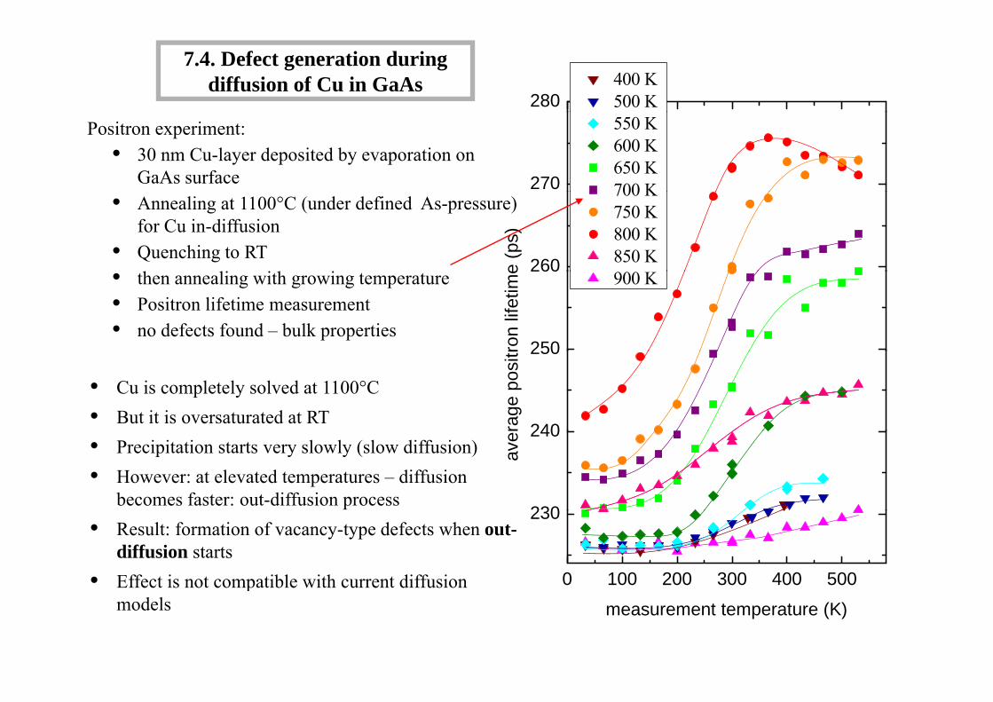
7.4. Defect generation during diffusion of Cu in GaAs
280400 K500 K
Positron experiment:• 30 nm Cu-layer deposited by evaporation on
GaAs surface 270
550 K600 K650 K700 K• Annealing at 1100°C (under defined As-pressure)
for Cu in-diffusion• Quenching to RT
h li i h i260
700 K750 K800 K850 Ke
(ps)
• then annealing with growing temperature• Positron lifetime measurement• no defects found – bulk properties
250
260900 K
ron
lifet
ime
• Cu is completely solved at 1100°C• But it is oversaturated at RT
240
250
rage
pos
itr
• Precipitation starts very slowly (slow diffusion)• However: at elevated temperatures – diffusion
becomes faster: out-diffusion process230
240
aver
• Result: formation of vacancy-type defects when out-diffusion starts
• Effect is not compatible with current diffusion 0 100 200 300 400 500
230
pmodels measurement temperature (K)
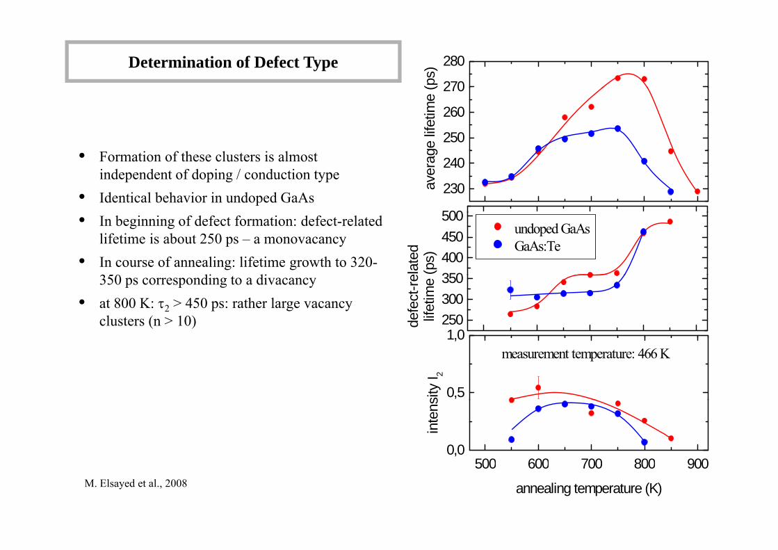
Determination of Defect Type270
280
(ps)
250
260
270
ge li
fetim
e (
• Formation of these clusters is almost independent of doping / conduction type
• Identical behavior in undoped GaAs 230
240
500
aver
ag
• In beginning of defect formation: defect-related lifetime is about 250 ps – a monovacancy
• In course of annealing: lifetime growth to 320-350 di di 350
400450500
undoped GaAsGaAs:Te
elat
ed(p
s)
350 ps corresponding to a divacancy• at 800 K: τ2 > 450 ps: rather large vacancy
clusters (n > 10)1 0
250300350
defe
ct-re
lifet
ime
0,5
1,0
sity
I 2
measurement temperature: 466 K
500 600 700 800 9000,0
inte
ns
500 600 700 800 900
annealing temperature (K)M. Elsayed et al., 2008

Coincidence-Doppler Spectroscopy at GaAs:Cu
• In high-momentum region (>10-2 m0c) annihilation with Core-electrons
2
4
Cuannihilation with Core-electrons dominate
• Electron momentum distribution of core electrons almost not changed
0
k G
aAs
Cu
gcompared to individual atoms
• Relatively easy to calculate• In example: the detected vacancies
1,00
atio
to b
ulk
In example: the detected vacancies have Cu atoms in closest vicinity
• Vacancies are obviously stabilized by Cu 0 75
Ra
0,75 VGa-SiGa SI-GaAs:Cu (annealed, at 500 K) SI-GaAs:Cu (as quenched, at 30 K)
0 10 20 30 pL (10-3 m0c)
V. Bondarenko, et al., Physica B 308-310 (2001)792-795
Martin-Luther-Universität Halle
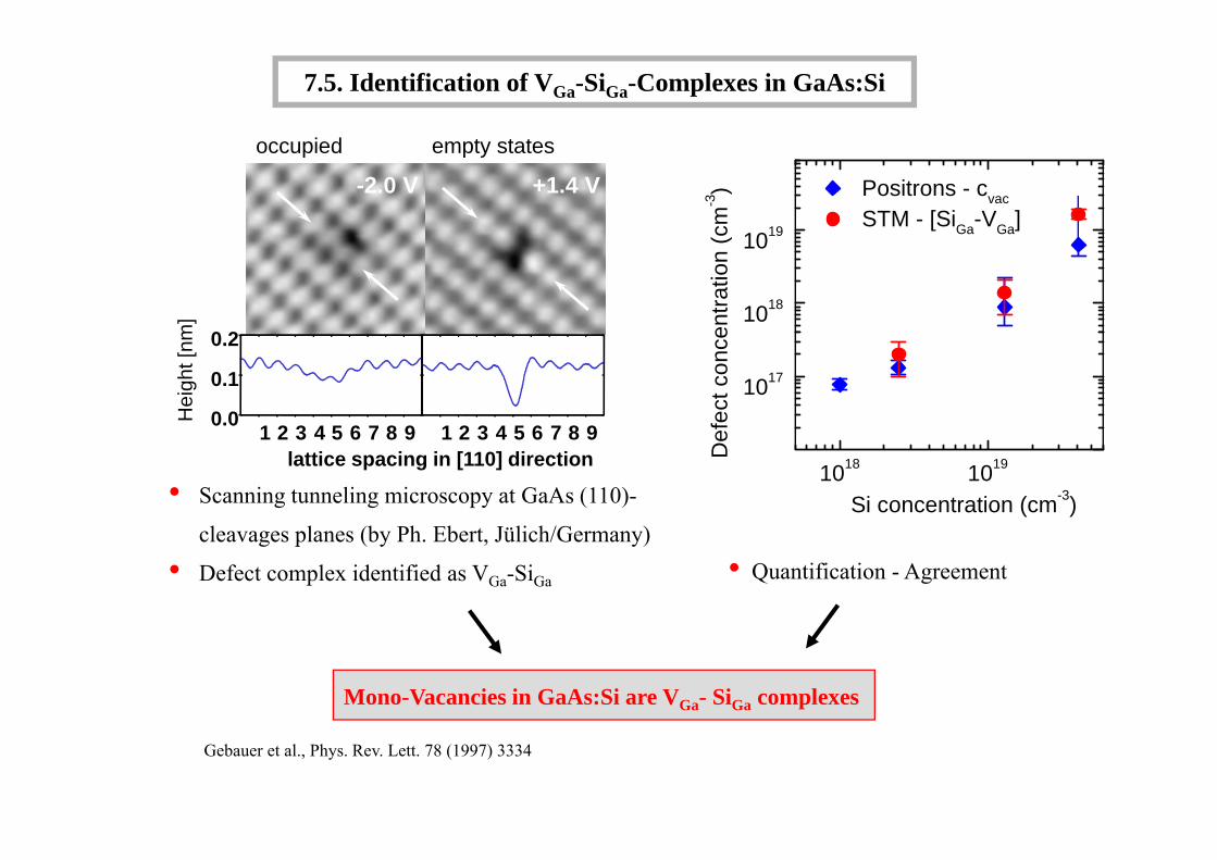
7.5. Identification of VGa-SiGa-Complexes in GaAs:Si
-2.0 V +1.4 Voccupied empty states
1019
Positrons - cvac STM - [SiGa-VGa] cm
-3)
0 2m] 1018
1019
entra
tion
(c
1 2 3 4 5 6 7 8 90.0
0.1
0.2
1 2 3 4 5 6 7 8 9
Hei
ght [
nm
1017
fect
con
ce
1 2 3 4 5 6 7 8 9 1 2 3 4 5 6 7 8 9lattice spacing in [110] direction
• Scanning tunneling microscopy at GaAs (110)-
l l (b Ph Eb Jüli h/G )
1018 1019
Si concentration (cm-3)
De
cleavages planes (by Ph. Ebert, Jülich/Germany)
• Defect complex identified as VGa-SiGa • Quantification - Agreement
Mono-Vacancies in GaAs:Si are VGa- SiGa complexes
Gebauer et al., Phys. Rev. Lett. 78 (1997) 3334

7.6. Defects in Si induced by Ion Implantation
• ion implantation is most important doping technique in planar technology
• main problem: generation of defects - positron beam measurements
(Eichler et al., 1997)
71

Defect density as function of deposited ion energy
RBS ltRBS results • Defect generation follows Chadderton‘s model of homogenous nucleation: L.T. Chadderton, Rad. Eff. 8 (1971) 1, ( )
• [defect] ~ dose0.5
• valid for RBS- and positron data
• only exception: Si self-implantation
• can be explained: extra Si atoms are interstitials and kill vacancies that are seen by positrons butand kill vacancies that are seen by positrons but not by RBS
positron results
(Eichler et al., 1997)72

7.7. Compensation mechanism of semi-isolating GaAs
• GaAs often needed as high-resistive wafer material• Dopant (impurity) level is about 1014 cm-3 - not low enough - but self-compensation was observed• self-compensation works only when [EL2] > [shallow acceptors] > [shallow donors]• (1) residual donors are compensated by shallow acceptors (carbon brought in by intension)• (2) remaining acceptors are compensated by deep donor – EL2-defect( ) g p p y p• (3) would need too high temperature, thus all carriers are compensated at “normal” temperatures• Required conditions can be fulfilled in pure semi-insulating GaAs by “doping” with C
73

Positron Study: The nature of the EL2 defect in GaAs
• one of mostly investigated defects
• exhibiting metastability at low T under light illuminationg
stable metastable(Dabrowski 1988, Chadi 1988)
• there were several structural models of EL2
• the above shown model was proven by positron annihilation
(Krause et al., 1990) 74

7.8. Defect engineering in II-VI compounds: Hg Vacancies in HgxCd1-xTe
• material for infrared detectors (has small band gap)• Hg diffuses very easily, high vapor pressure of Hg at relatively low temperatures• VHg is acceptor and dominates electrical and optical behaviorg• experimental finding: strong changes of [VHg] in THM-grown crystals
75R. Krause, et al., J. Cryst. Growth 101 (1990) 512

Control of VHg concentration
• Concentration of Hg vacancies can be controlled by annealing under defined vapor pressure of Hg
• all technological steps must be performed under Hg vapor pressure
76

7.9. Defects in high-energy self-implanted Si: The Rp/2 effect
• after high-energy (3.5 MeV) self-implantation of Si (5x1015 cm-2) and RTA annealing (900°C, 30s): two new gettering zones appear at Rp and Rp/2 (Rp = projected range of Si+)
• visible by SIMS profiling after intentional Cu contaminationy p g
TEM image by P. Werner, MPI Halle
• at Rp: gettering by interstitial-type dislocation loops (formed by excess
1017
on (c
m-3)
SIMS interstitials during RTA)
• no defects visible by TEM at Rp/2
• What type are these defects?
1016
once
ntra
ti
RR /2
What type are these defects?
0 1 2 3 41015Cu
co
Depth (μm)
RpRp/2
Depth (μm)
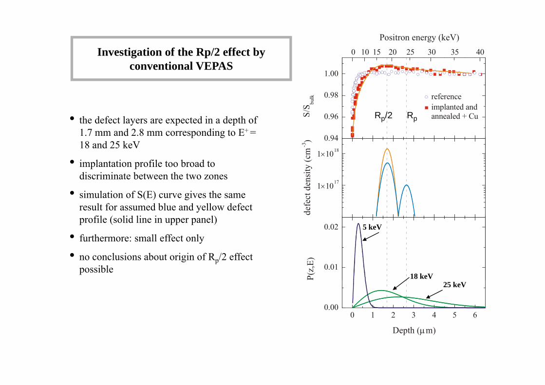
Investigation of the Rp/2 effect by Positron energy (keV)
40 35 30 25 20 15 10 0
conventional VEPAS
0.98
1.00
S bulk
reference i l t d d
• the defect layers are expected in a depth of 1.7 mm and 2.8 mm corresponding to E+ = 18 and 25 keV
0.94
0.96
18
S/S
m -3
)
implanted andannealed + CuRpRp/2
• implantation profile too broad to discriminate between the two zones
• i l ti f S(E) i th17
1 10 ×
1 10 ×
18
dens
ity (c
m
• simulation of S(E) curve gives the same result for assumed blue and yellow defect profile (solid line in upper panel)
• f th ll ff t l0.02
defe
ct
5 keV• furthermore: small effect only
• no conclusions about origin of Rp/2 effect possible 0.01
P(z,
E)
18 keV
0 1 2 3 4 5 6 0.00
P
25 keV
Depth ( μ m)

Enhanced depth resolution by using the Positron Microscope
positronmicrobeamE = 8 keV • sample is wedge-shaped
scan direction
defect depth
p g ppolished (0.5…2°)
• layer of polishing defects must be thin compared to e+
lateral resolution1 ... 2 mμ
α = 0.6°10 mμ
pimplantation depth
• best: chemo-mechanical polishingp g
s)po
sitro
nlif
etim
e (p
s
τbulk
τdefect
scan width0 1 mm

0,6
0,80 1 2 3 4 5 6
fraction of trapped positronsη
First defect depth profile using Positron Microscopy
0,4
defect-relatedlifetime
450
η
• 45 lifetime spectra: scan along wedge
• separation of 11 µm between two measurements d d h diff f (
divacancy-typedefect
microvoidslifetime
350
400
τ 2 (ps
)corresponds to depth difference of 155 nm (a = 0.81°)
• beam energy of 8 keV: mean penetration depth is b 400 i d h l i
360
380
R /2
Silicon self-implantation - 3.5 MeV, 5×1015 cm-2
- annealed 30s 900°C(ps)
about 400 nm; represents optimum depth resolution
• no further improvement possible due to positron diffusion: L+(Si @ 300K) » 230 nm
320
340
Rp/2
Rp
- Cu contaminated
e lif
etim
e (
• both regions well visible:
− vacancy clusters with increasing density down to 2 µm (Rp/2 region)
300
320
surface
aver
age
Cu SIMS-Profil
to 2 µm (Rp/2 region)
− in Rp region: lifetime τ2 = 330 ps; corresponds to open volume of a divacancy; must be stabilized or being part of interstitial-type
0 1 2 3 4 5 6260
280 surfacebulk silicon
d th ( )
• excellent agreement with gettered Cu profile
stabilized or being part of interstitial type dislocation loops
depth (µm)
Martin-Luther-Universität Halle
R. Krause-Rehberg et al., Appl. Phys. Lett. 77 (2000) 3932

7.10. Defects in GaAs introduced by wafer cutting
50 mμ• cutting of wafer with diamond-saw (by wire and blade saws)• after cutting: surface destroyed, defects several µm deep• defect profile reaches far into the interior of the wafer• Point defects can be studied e.g. by positron annihilation• careful etching and polishing necessary• Demand of technology: wafer roughness must be < 1 µm for a complete 6" wafer
81
Demand of technology: wafer roughness must be < 1 µm for a complete 6 wafer

Cutting defects in GaAs: polishing
Atomic force microscopy before/after polishing and etching
0.8
1.0
60
70
0 4
0.6
0.8
ght (
nm)
30
40
50
ght (
nm)
0 0
0.2
0.4
heig
0
10
20
30
heig
82
0 200 400 600 800 1000 1200 1400 16000.0
length (nm)0 500 1000 1500 2000 2500 3000 3500
0
length (nm)

Positron Study of Damage of Wafer Surface by a Diamond Saw
Damage depth as functionof saw speed9.0
9.5
m) of saw speed
7.5
8.0
8.5
e de
pth
(μm
6.0
6.5
7.0
dam
age
1 2 3 4 5 65.5
advance of the saw blade (arb. units)
• maximum positron energy 40 keV: mean implantation depth = 3.3 µmp p µ
• step-wise etching (about 2…3 µm per step) of surface by (H2O2-NH3)
• repeated positron beam measurementi f diff t fil
F. Börner et al., J. Appl. Phys. 84 (4), 2255-2262 (1998)
• superimpose of different profiles
Martin-Luther-Universität Halle

7.10. Smart-Cut process of GaN
Technological context: Hetero-epitaxial growth of WBG materials on foreign substrates leads unavoidably to the formation of growth-related defects such as dislocations, stacking faults and twins that occur to relax the strain which significantly limits the quality of the grown structures with undesirable impact on devices performance. with undesirable impact on devices performance.
What to do? Direct wafer bonding in combination with hydrogen ion-cutting is a promising stratagem to integrate bulk quality thin layers onto various host materials achieving a wide variety of heterostructures sometimes inconceivable by epitaxy. Having bulk properties, these new materials
i i f l t f b i ti f WBG b d d i h h h f hit are very promising for a low cost fabrication of WBG-based devices such as phosphorous-free white LED and high performance laser diodes.
H Implantation (high dose)(high dose)
R
Recyclable wafer
WBG
H rich zone
Host substrateNew
heterostructure
~550°CRpRp
Wafer-Bonding SplittingIon-Cut Process

SRIM Simulations
defect layer at about 350 nm
Implantation: energy 50 keV,
fl 2 6 1017 H/ 2fluence 2.6x10¹⁷ H/cm2

During implantation: nanobubbles 1-2 nm are formed

600°C
450°C 500°C

Understanding basic mechanisms of ion-cut process
• In order to draw a precise mechanistic picture of H-induced splitting of WBG materials a deep investigation thermal evolution of H-defect complexes is required
High magnification XTEM image showing id ( b bbl ) hi h
• Simulated defect concentration fits to position of platelets
V0
50 nm
nanovoids (or nanobubbles) which appear bright.
H
VGa
VN
400
200
pth
[nm
]
250 nm
H
800
600Dep
Splitting at 600 oC

Doppler Broadening Measurements
• Slow positron DOBS of implanted GaN sample: results show strong defect signal
• 50 keV protons and 2 6x10¹⁷ H/cm250 keV protons and 2.6x10 H/cm
nanovoids
6.5 %

Positron Lifetime Experiments at PLEPS @ FRM-II

3-component decomposition of lifetime spectra
Positronium Formation!
500 ps

8. Conclusions8. Conclusions
• Positrons Annihilation Spectroscopy is a unique tool for studying nanoscopic open-volume defects, such as vacancies, vacancy clusters, dislocations, nano-precipitates, nano-porosity, grain boundaries of nano-grains, acceptors (in semiconductors)
• high sensitivity starts at 5x1014 cm-3 (is about 10-7)• defect type and density may be determined• Coincidence Doppler Broadening – chemical information on surrounding of
defect• in semiconductors: sensitivity for charge state of defects• different methods allow investigation of thin layers (< 1 μm) up to cm thick
samples• positron micro-beams have about 2 μm lateral resolution• user-dedicated positron sources with high-intensity sources now available
92

9. Literature9. Literature
• R. Krause-Rehberg, H.S. Leipner „Positron Annihilation in Semiconductors“; Springer 1998
• P. Coleman „Positron Beams and their applications“; World
Scientific 2000Scientific 2000
• M. Charlton, J.W. Humbertson „Positron Physics“; Cambridge
University Press 2001
• New book project Positron Annihilation“:New book project „Positron Annihilation :
http://positron.physik.uni-halle.de/book_project
93