Embed Size (px)
Citation preview
19SV111
SHARP SERVICE MANUAL S99N919SV1 111
GAME TElEVISION SIGMA 9400 CHASSIS
Chassis No. 19M1
MODEL 19SV111 In the interests of user-safety (Required by safety regulations in some countries) the set should be restored to its original condition and only parts identical to those specified should be used.
c~~ -. tl L'QIV/IliU ~ Q '?, 0 c.. N 1 '2DZ. <!.E "Z "Z lf'l ot ~ u
Z. ~2DC.t.dl-~ e.l'2.1v\Qib ¢lPB'3 C..~ 5 A $ ~D,_},q ~r CONTENTS
Page • IMPORTANT SERVICE SAFETY PRECAUTION ..................................................... 2 • ELECTRICALSPECIFICATIONS ............................................................................ 3 • LOCATION OF USER'S CONTROLS .................................................................... _ 4 • REMOVAL OF CABINET .................................................................................... _ 6 • INSTALLATION AND SERVICE INSTRUCTIONS .................................................... 8 • TROUBLE SHOOTING TABLE .............. ... ......... ............................... ............ .......... 10 • CHASSIS LAYOUT .................................................. · ...... · .................. · ......... · ........... 16 • PRINTED WIRING BOARD ASSEMBLIES ............................................................... 17 • BLOCK DIAGRAM ··············'·························--···--···--············--····················--······ 21 • SOLID STATE DEVICE BASE DIAGRAM ............................................................... 26 • SCHEMATIC DIAGRAM AND WAVEFORMES . . . . . . . . . . . . . . . . . . . . . . . . . . .. . . . . . . . .. . . . . . . . . . . .. . . . . . . 28 • REPLACEMENT PA·RTS LIST ................................................................................ 35 ·• PACKING OF THE SET . . . . . . . . . . .. . . . ... . ... . ..... . . ... . . ... . . ... . . . .. . . .. . . .. . . ... . . . .. . . .. . . . . . . . . . . ... . . .. . 44
SHARP ELECTRONICS CORPORATION Service Headquarters: Sharp PI aza, Mahwah, New Jersey 07 430-2135 Phone; (20 1) 512-0055
'19SV111
IMPORTANT SERVICE SAFETY PRECAUTION • Service w_ork should be performed only by qualified service technicians who are
thoroughly familiar with all safety checks and servicing guidelines which follow:
WARNING 1. For continued safety, no modification of any
circuit should be attempted. 2. Disconnect AC power before servicing. 3. Semiconductor heat sinks are potential shock
hazards when the receiver is operating. 4. The chassis in this receiver has two ground
systems which are separated by insulation material. The non-isolated (hot) ground system is for the + B voltage regulator circuit and the horizontal output circuit. The isolated ground sy5tem is for the low + B DC voltages and the secondary circuit of the high voltage transformer. To prevent electrical shock use an isolation transformer between the I i ne cord and power receptacle, when servicing this chassis.
SERVICING OF HIGH VOLTAGE SYSTEM AND PICTURE TUBE When servicing the high voltage system, remove the static charge by connecting a 10k ohm resisto-r in series with an insulated wire (such as a test probe) between the picture tube ground and the anode lead. {AC cord should be disconnected from AC outlet.) 1. Note that the picture tube in this receiver
employs integral implosion protection. 2. Replace with tube of the same type number for
continued safety. 3. Do not I i ft picture tube by the neck. 4. Handle the picture tube only when wearing
shatterproof goggles and after discharging the high voltage anode completely.
X-RADIATION AND HIGH VOLTAGE LIMITS 1. All service personnel should be aware of the
procedures and instructions covering Xradiation. The only potential source of X-ray in current solid state TV receivers is the picture tube. However, the picture tube does not emit measurable X-Ray radiation if the high voltage is as specified in the "High Voltage Check" instructions.lt is only when high voltage is excessive that X·rad iation is capable of penetrating the picture tube shell which includes lead in glass material. The important precaution is to keep high voltage below the maximum level specified.
2
2. It is essential that servicemen have available at all times an accurate high voltage meter. The calibration of this meter should be checked periodically.
3. High voltage should always be kept at the rated value -no higher. Operation at higher voltages may cause a failure of the picture tube or high voltage circuitry and, under certain conditions, may produce radiation in excess of desirable levels.
4. When the high voltage regulator is operating properly there is no possibility of an Xradiation problem. Every time a color chassis is serviced, the brightness should be tested while monitoring high voltage with a meter to be certain that it does not exceed the specified value and is regulated correctly.
5. Do not use a picture tube other than that specified, and do not make unrecommended circuit modifications to the high voltage circuitry.
6. When trouble shooting and taking test measurements on a receiver with excessively high voltage,avoid being unnecessarily dose to the receiver. Do not operate the receiver longer than is necessary to locate the cause of excessive voltage.
FIRE AND SHOCK HAZARD CHECKS Before returning the receiver to the user, perform the following safety checks: 1. Inspect all lead dress to make certain that leads
are not pinched, and check that hardware is not lodged between the chassis and other metal parts in the receiver.
2. Inspect all protective devices such as non· metallic control knobs, insulating materials, cabinet backs, adjustment and compartment covers or shields, isolation resistor-capacity networks, mechanical insulators, etc.
3. To be sure that no shock hazard exists, check for current I eakage in the foil owing manner:
• PI ug the AC cord d i recti y into a 120 volt AC outlet, (Do not use an isolation transformer for this test).
• Using two clip leads, connect a 1.5k ohm, 10 watt resistor paralleled by a 0.1SuF capacitor in series with all exposed metal cabinet parts and a known earth ground, such as an electrical conduit or electrical ground connected to an earth ground.
19SV111
IMPORTANT SERVICE SAFETY PRECAUTION (Continued)
• Use an AC voltmeter having with 5000 ohm per volt, or higher, sensitivity to measure the AC voltage drop across the resistor.
• Make contact with the test probe on all exposed metal parts having a return path to the chassis (antenna, metal cabinet, screw heads, knobs and control shafts, escutcheon, etc.) and measure the AC voltage drop across the resistor. All checks must be repeated with the AC cord plug connection reversed (if necessary, a nonpolarized adapter plug may be used only for the purpose of completing these checks). Any current measured must not exceed 0.5 milliamps. Any measurements not within the limits outlined above are indicative of potential shock hazard and corrective action must be taken before returning the set to the customer.
SAFETY NOTICE Many electrical and mechanical parts in television receivers have special safety-related characteristics. These characteristics are often not evident from visual inspection, nor can protection afforded by them be necessarily increased by using rep I acement components rated for higher voltage, wattage, etc. Replacement parts which have these special
safety characteristics are ide nti fi ed in this manual; electrical components having such features are identified by ".&"and shaded areas in the Replacement Parts Lists and Schematic Diagrams. For continued protection, replacement parts must be identical to those used in the original circuit. The use of a substitute replacement parts which do not have the same safety characteristics as the factory recommended replacement parts shown in this service manual, may create shock, fire, X-radiation or other hazards.
!~ AC
VOLTMETER
TO EXPOSED METAL PARTS
CONNECT TO KNOWN EARTH GROUND
ELECTRICAL SPECIFICATIONS VHF ANTENNA INPUT IMPEDANCE ............................... ,. ..................... 75 ohm Unbalanced UHF ANTENNA INPUT IMPEDANCE ...................................................... 300 ohm Balanced CONVERGENCE .................................................................................. Magnetic FOCUS ................................................................................................. Hi-Bi-Potential Electrostatic AU 010 POWER OUTPUT RA Tl NG ........................................................ 1.2 W (at 10% distortion) INTERMEDIATE FREQUENCIES
Picture IF Carrier Frequency .......................................................... 45.75 MHz Sound IF carrier Frequency ............................................................ 41.25 MHz Color Sub-Carrier Frequency .......................................................... 42.17 MHz (Nominal)
PICTURE SIZE ...................................................................................... Approx. 185 sq. in. POWER IN PUT ..................................................................................... 120 V AC 60Hz POWER RATING .................................................................................. 95 W SPEAKER SIZE ..................................................................................... 4• PM, 0.52 oz. Mag. VOICE COIL IMPEDANCE ......... · .... · ................ · .............................. · · · ... 8 ohm at 400 Hz SWEEP DEFLECTION ........................................................................... Magnetic TUNING RANGES····--· .......................................................................... VHF-Channels 2 thru 13
UHF-Channels 14 thru 83 CATV Channels 1 thru 65,
Specifications are subject to change without prior notice. 95 thru 99 (EIA, Channel Plan)
3
19SV111
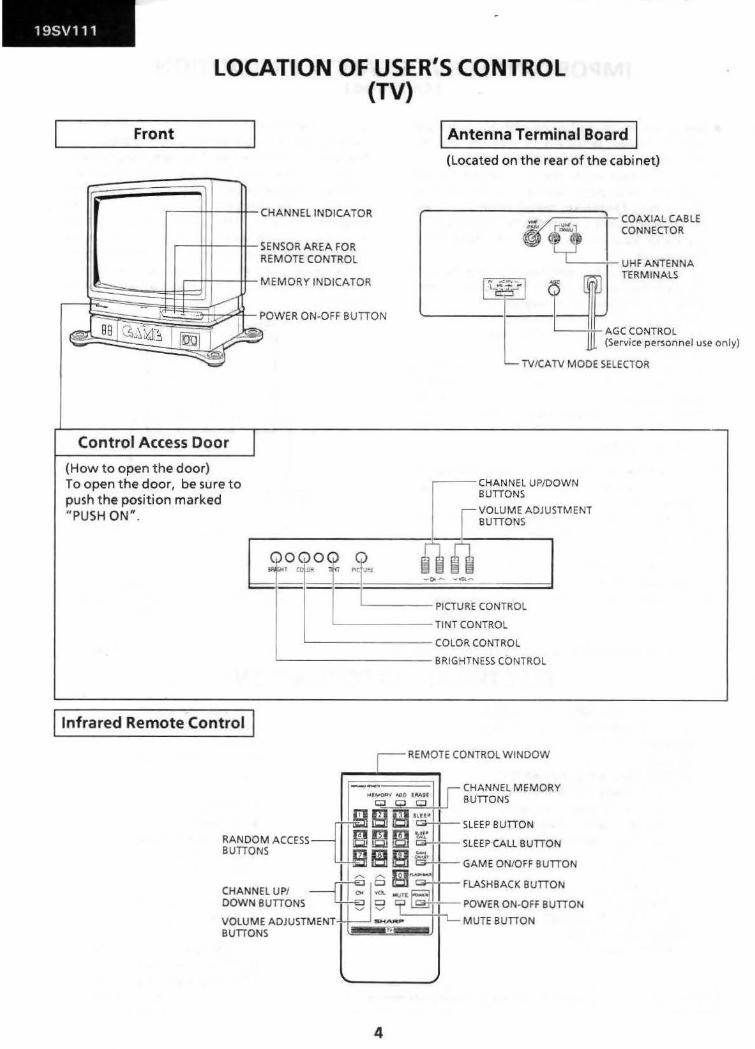
Front
LOCATION OF USER'S CONTROL (TV)
I Antenna Terminal Board I (Located on the rear of the cabinet)
r--__;l-l-11 11----#-CHANNEliNDICATOR
r----+T-11----H- SENSOR AREA FOR
REMOTE CONTROL
E,;~ COAXIAL CABLE
~ "~ I CONNECTOR
LC.._I_ UHF ANTENNA
b _lr--f++--+1- MEMORY INDICATOR
~1~~-;;~.SI ~~;. ~?""~_...........,;...-l~ lb. =POWER ON-OFF BUTION
~ ~ TERMINALS
'-----~-'L-f= bJ ~~~~~~~~~n•l ""only) ~ ee J C?..;~~ 1 ~I~ ~
Control Access Door
(How to open the door) To open t he door, be sure to push t he position marked "PUSH ON".
I
L TV/CATV MODE SELECTOR
,.----- CHANNEL UP/DOWN BUTTONS
[
VOLUME ADJUSTMENT BUTTONS
L~.o -~ . t o==_ o=.,._ ====:I
PICTURE CONTROL
'--------TINT CONTROL
'---------COLOR CONTROL
'-------------BRIGHTNESS CONTROL
! Infrared Remote Control I REMOTE CONTROL WINDOW
CHANNEL MEMORY 0 0 BUTTONS
-tmm .. u•l ' !CJ 1CJ c:::3--l+- SLEEP BUTTON
RANDOM ACCESS e e ilL SLEEP CALL BUTTON suTToNs m m §· II
II,.... ~ !CI ---I I GAME ON/OFF BUTTON
CHANNEL UP/ ~ :;_ ~ ~FLASHBACK BUTTON
DOWN BUTTONS ~ 9 Cfl ~I I L POW€RON-OFF BUTTON
VOLUME ADJUSTMENT ....,_ MUTE BUTTON BUTTONS "
4
GAME ON/OFF
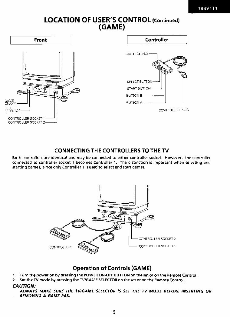
LOCATION OF USER'S CONTROL (Continued) (GAME)
Front I Controller
CONTROL PAD
START BUTTON
BUTTON B----'
BUTTON A------'
CONTROLLER PLUG
CONTROLLER SOCKET 1 CONTROLLER SOCKET 2
CONNECTING THE CONTROLLERS TO THE TV
19SV111
Both controllers are identical and may be connected to either controller socket. However, the controller connected to controller socket 1 becomes Controller 1, The distinction is important when selecting and starting games, since only Controller 1 is used to select and start games.
CONTROLLER SOCKET 2
CONTROLLERS CONTROLLER SOCKET 1
Operation of Controls (GAME) 1. Turn the power on by pressing the POWER 0 N·O F F BUTTON on the set or on the Remote Control. 2. Set the TV mode by pressing the TV/GAME SELECTOR on the set or on the Remote Control.
CAUTION: ALWAYS MAKE SURE THE TVIGAME SELECTOR IS SET THE TV MODE BEFORE INSERTING OR REMOVING A GAME PAK.
5
19SV111
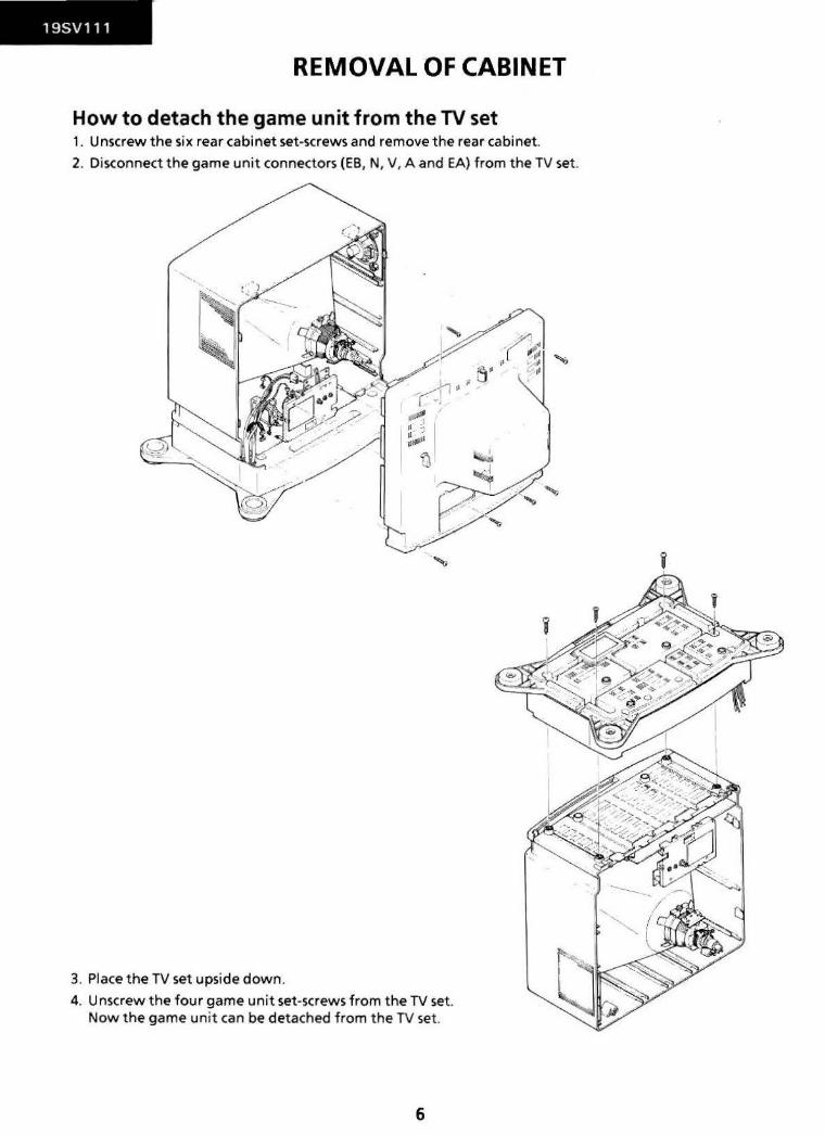
REMOVAl OF CABINET
How to detach the game unit from the TV set 1. Unscrew the six rear cabinet set-screws and remove the rear cabinet.
2. Disconnect the game unit connectors (EB, N, V, A and EA) from the TV set.
3. Place the TV set upside down.
4. Unscrew the four game unit set-screws from the TV set. Now the game unit can be detached from the TV set .
6
19SV111
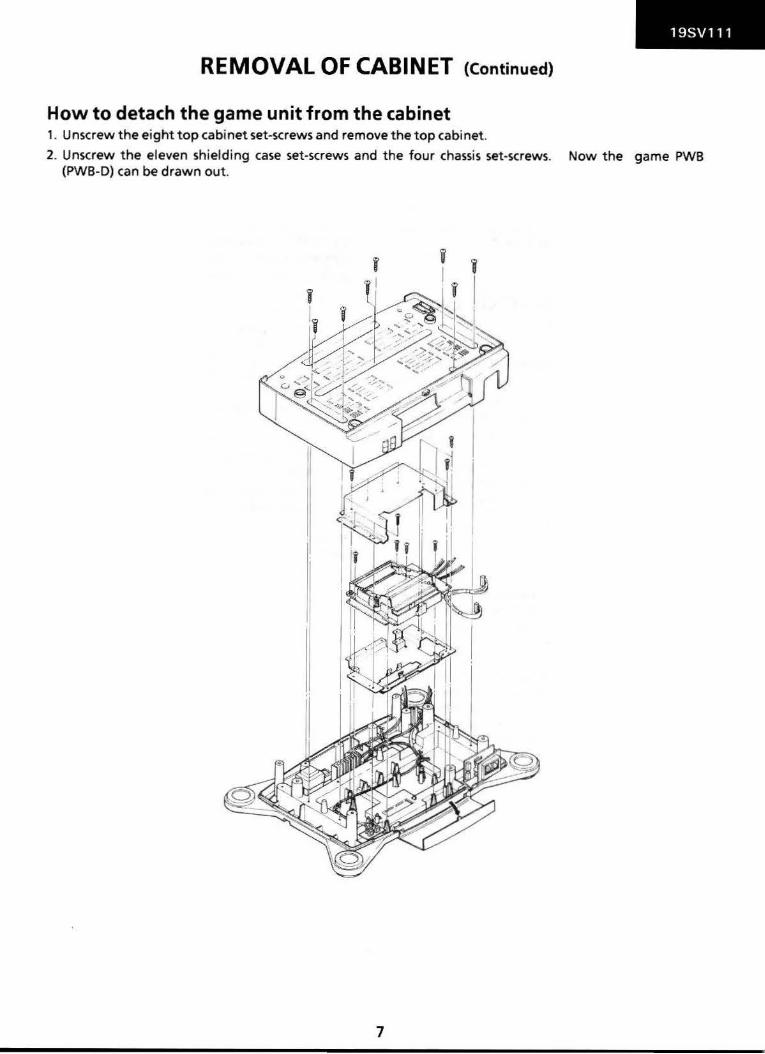
REMOVAL OF CABINET (continued)
How to detach the game unit from the cabinet 1. Unscrew the eight top cabinet set-screws and remove the top cabinet.
2. Unscrew the eleven shielding case set-screws and the four chassis set-screws. Now the game PWB (PWB-D) can be drawn out.
7
19SV11 'I
INSTALLATION AND SERVICE INSTRUCTIONS Note: (1) When performing any adjustments to resistor controls and transformers use
non-metallic screwdriver or TV alignment tools. (2) Before perfoming adjustment, TV set must be on at least 15 minutes.
CIRCUIT PROTECTION The receiver is protected by a 4.0A fuse (F701), mounted on PWB-A, wired into one side of the AC line input.
X-RADIATION PROTECTOR CIRCUIT TEST After service has been perlormed on the horizontal deflection system, high voltage system, or+ B system, the XRadiation protection circuit must be tested for proper operation as follows: 1. Apply 120V AC using a variac transformer for
accurate input voltage. 2. Allow for warm up and adjust all customer
controls for norma I picture and sound. 3. Check the voltage of test point TP601. (It's
voltage should be about 18V DC.) 4. Connect the pin (6) of IC501 to TP601 through
a short clip lead. In this case, the operation of horizontal oscillator is stopped.
5. To start operation, remove the above short clip lead and touch the TP602 to chassis ground (TP603) with a short clip lead. In this case remove short c I i p I ead as soon as the set operates again with a normal picture.
6. Connect TP651 to TP652 and see that the operation of horizontal oscillator then stops. Next, make sure that the set operates with a normal picture by the method of StepS.
7. If the operation of the horizontal osc. does not stop in steps 4 and 6, the circuit must be repaired before the set is returned to the customer.
8
HIGH VOLTAGE CHECK High voltage is not adjustable but niust be checked to verify that the receiver is operating within safe and efficient design limitations as specified checks should be as follows: 1. Connect an accurate high voltage meter to the
CRT anode. 2. Operate receiver for at least 15 minutes at
120V AC line voltage, with strong air signal or a proper I y tuned in test signa I.
3. Set SW851 on PWB-B to "OFF" (center) position. Note that I o.ss of I u m i nance wi 11 occur.
4. Rotate Screen control (on T652) to minimum (CCW) end of its rotation.
5. The reading sho.uld be approximately 26.5kV at zero beam.
If a correct reading cannot be obtained, check circuitry for malfunctioning components. Upon completion of voltage check, readjust screen control for proper operation and set SW851 to "ON" position.

19SV111
INSTALLATION AND SERVICE INSTRUCTIONS (Continued)
FIELD ADJUSTMENT
• RF-AGCADJUSTMENT 1. Select a local channel. 2. Turn RF-AGC control (R214) fully ciO<kwise.
As a result noise appears on picture, then slowly turn the RF-AGC control (R214) counterclockwise until noise disappears.
3. Check that no noise appears on other channels.
• SUB-BRIGHTNESS CONTROL 1. Select a local channel. 2. Turn Picture control (a part of R462) fully
clockwise and set Brightness control (a part of R462) at the center position.
3. Turn Sub-Brightness control (a part of R462) to obtain normal brightness of the picture.
• HORIZONTAL CENTERING 1. Select a local channel. 2. Adjust the Horizontal Centering Switch
(SW7 51 ) on PWB-C to best picture position.
• VERTICAL SIZE ADJUSTMENT 1. Select a local channel. 2. Turn fully counterclockwise the Brightness and
Picture controls to dim screen (in the state where the top and bottom of picture cam be recognized.}
3. Adjust Vertical Size control {a part of R462) for approximately 1/8 to 1/4 inch over-scan at top and bottom of picture screen.
• FOCUS ADJUSTMENT 1 . Select a I ocal channel. 2. Set Brightness and Picture controls at a normal
viewing level. 3. Adjust focus control (part of T652) for sharp
scanning lines and/or sharp picture.
9
NOTE 1: All field adj-Ustments mentioned can be performed without test equipment.
NOTE 2: As this model has "Built in AFT", AFT is always in "ON" position. If AFT should be "OFF", short between TP1003 and TP1004.
NOTE 3: After servicing the set check that the aging switch SW1801 is set at "OFF" position. This aging switch is to be used only for the factory inspection; at "ONH position, it won't allow the set to be turned off.
195V111
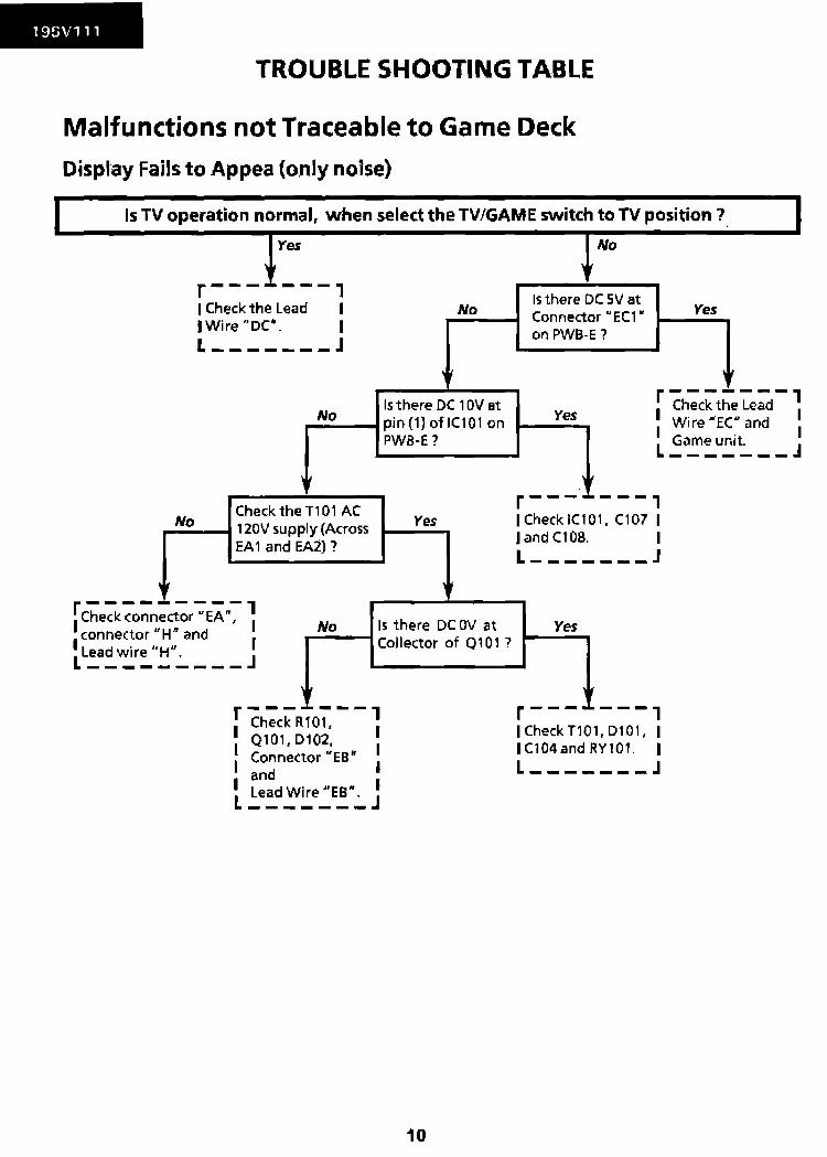
TROUBLE SHOOTING TABLE
Malfunctions not Traceable to Game Deck
Display Fails to Appe-a (o.nly noise)
I Is TV operation normal, when select the TV/GAME switch to TV position?
Yes \ ~
r---··---, 1 Check the Lead I No 1 Wire "oc•. 1
L-------J
Is there DC 1 OV at .... N_o_.....,. pin (1) of IC101 on
PWB-E?
Check the T1 01 AC r--No_---1 120V supply {Across
EA 1 and EA2)?
,~
r----··----,
Yes
No
' lr
Is there DC SV at Connector "EC1" on PWB-E?
Yes
'~ r-- -· ... -- -, I Check IC101, C107 I I and C108. I
L-------J
1 Check connector "EA", 1 I connector "Hn and I
Lead wire "H".
No Is there DC OV at ....----tcollector of Q101? ...,..._ .......
Yes
L--,._- ... _~'11111111111-J
' r Ch;ck Rto7.- -, Q101, D102, I
1 Connector "EB" 1 1 and 1 I Lead Wire "EB". I L-------J
10
r ..... ..-.~ .......... ___ , I Check T101, D101, I I C104 and RY101. I L _______ J
Yes
I

19SV111
TROUBLE SHOOTING TABLE (Continued)
Controller Doeswt Function.
Yes
Controller faulty.
Selection and starting not possible or selection mark continues moving.
Do symptoms change when controller cord bent?
No Yes It
r--· .. --, : Controller : I cord faulty. I L _____ J
Is controller plug- to- socket contact good?
'~ ~Ched.;,;r~l;, ;rd ~ soldenng cond1t1on, 1
:wire broken or 1 shorted. L ________ .J
Is problem corrected by replacing controller ?
Pause occurs during game or pause occurs when button A pressed during game.
Controller cord faulty.
r ___ j ____ , : Check some :
1 buttons. 1
L--------.J
Some buttons don't operate or some buttons remain ON.
Are button contacts OK?
No j Yes
' rche~ tl;e-PWBin7id""; ~ 1 the controller. 1 I (Checks and ford irty 1 Lo:_d:_m_:ged ~o~t~~· .J
11
No
Game Deck faulty.
Are controller socket pins and harnesses (PWB-G) OK?
Check continuity between controller socket (PWB-G) and Game Unit.
r--------, I I I Game Unit faulty. I I I L--------J
19SV111
TROUBLE SHOOTING TABLE (Continued)
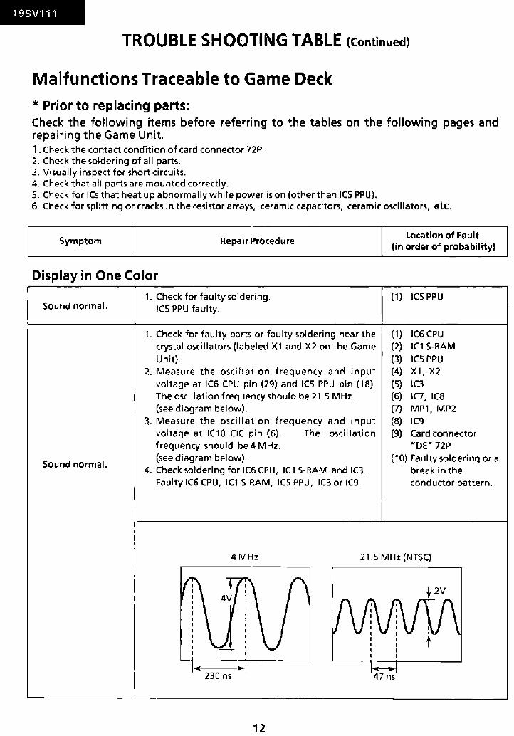
Malfunctions Traceable to Game Deck
* Prior to replacing parts: Check the following items before referring to the tables on the following pages and repairing the Game Unit. 1. Check the contact condition of card connector 72P. 2. Check the soldering of all parts. 3. Visually inspect for short circuits. 4. Check that all parts are mounted correctly. 5. Check for ICs that heat up abnormally while power is on (other than ICS PPU). 6. Check for splitting or cracks in the resistor arrays, ceramic capacitors, ceramic osci II ators, etc.
Symptom Repair Procedure
Display in One Color
Sound normal.
Sound normal.
1. Check for faulty soldering. ICS PPU faulty.
1 . Check for faulty parts or faulty soldering near the crystal oscillators (labeled X1 and X2 on the Game Unit).
2. Measure the osci!! ati on frequency and input voltage at IC6 CPU pin (29) and res PPU pin (18). The oscillation frequency should be 21.5 MHz. (see diagram below}.
3. Measure the oscir ration frequency and input voltage at rC10 CIC pin (6) . The oscillation frequency should be 4 M Hz. (see diagram below).
4. Check soldering for IC6 CPU, IC1 5-RAM and IC3. Faulty rc6 CPU, ret 5-RAM, res PPU, rc3 or IC9.
Location of Fault (in order of probability)
(1) ICS PPU
(1) IC6CPU (2) IC1 5-RAM (3) ICS PPU {4) X1, X2 (5) 1(3
(6) 1(7, 1(8 (7) MP1, MP2 (8) IC9 (9) Card connector
"DE" 72P ( 1 0) Faulty soldering or a
break in the conductor pattern.
4MHz 2 t .5 MHz (NTSC)
230 ns
12
19SV111
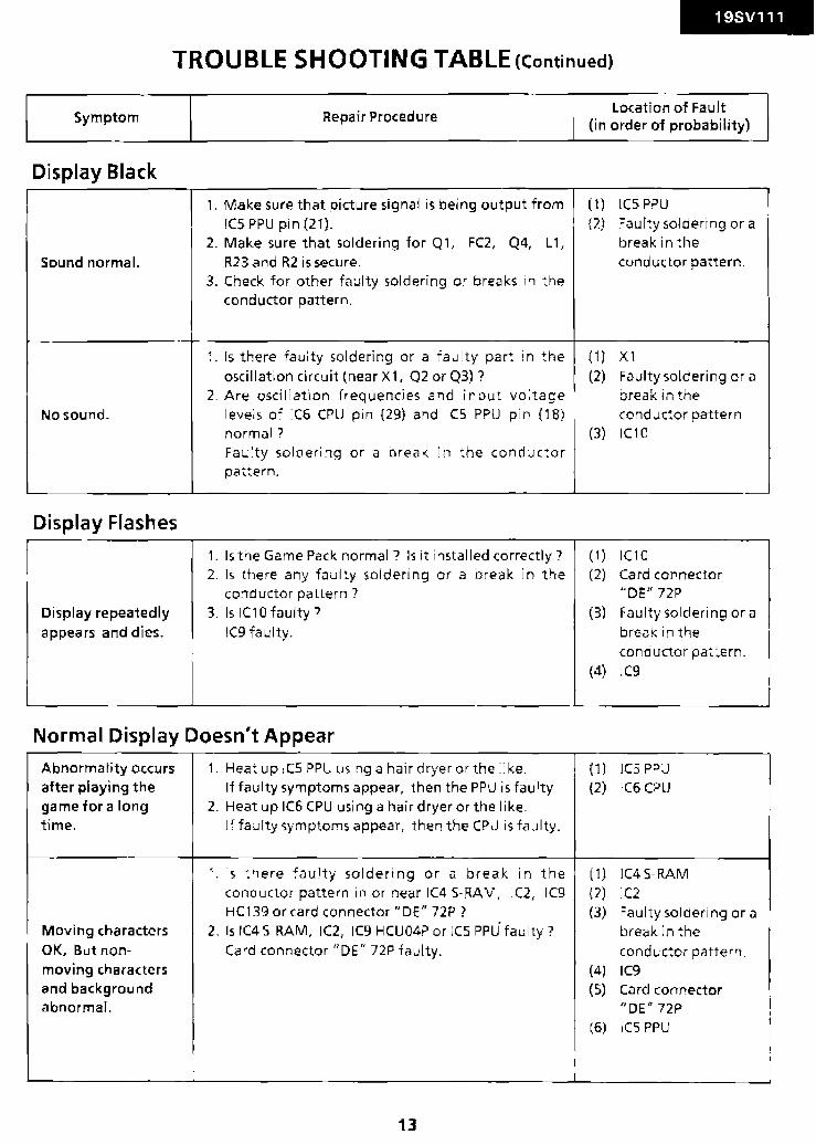
TROUBLE SHOOTING TABLE <continued)
Symptom
Display Black
Sound normal.
No sound.
Repair Procedure
1. Make sure that picture signal is being output from ICS PPU pin (21).
2. Make sure that soldering for Q 1, FC2, Q4, l1, R23 and R2 is secure.
3. Check for other faulty soldering or breaks in the conductor pattern.
1. Is there faulty soldering or a fa u I ty part in the
asci llation circuit (near X 1, 02 or 03) ? 2_ Are oscillation frequencies and input voltage
levels of ICG CPU pin (29) and ICS PPU pin ( 18)
normal? Faulty soldering or a break in the conductor pattern.
Location of Fault (in order of probability)
(1) ICSPPU (2) Faulty soldering or a
break in the conductor pattern.
(1) Xl
(2) Faulty soldering or a break in the conductor pattern.
(3) IC10
~----------------~------------------~------------------~------------------·--
Display Flashes
1. Is the Game Pack normal' Is it installed correctly? (1) 1(10 2. Is there any fau I ty soldering or a break in the (2) Card connector
conductor pattern I "DE" 72P Display repeatedly 3. Is 1(1 0 faulty., (3) Faulty soldering or a appears and dies. IC9 faulty. break in the
conductor pattern_ (4) 1(9
Normal Display Doesn't Appear
Abnormality occurs 1. Heat up ICS PPU using a hair dryer or the I ike_ ( 1) ICS PPU after playing the If faulty symptoms appear, then the PPU is faulty. (2) iC6 CPU game for a long 2_ Heat up ICG CPU using a hair dryer or the like_ time. If faulty symptoms appear, then the CPU is faulty.
1. Is there faulty soldering or a break in the ( 1) IC45-RAM conductor pattern in or near IC4 S·RAM, IC2, IC9 (2) IC2 HC 139 orca rd connector "DE" 72P ? (3) Faulty soldering or a
Moving characters 2. Is IC4 5-RAM, IC2, 1(9 HCU04P or lC5 PPU faulty? break in the OK, But non- Card connector "DE" 72P faulty. conductor pattern. moving characters (4) IC9 and background (5) Card connector abnormal. "DE" 72P
(6) IC5 PPU
13
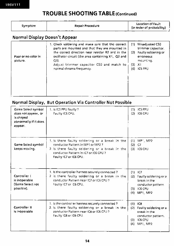
19SV111
TROUBLE SHOOTI~G TABLE<continued)
Symptom Repair Procedure Location of Fault
(in order of probability)
Normal Display Doesnlt Appear
1. Check soldering and make sure that the correct (1) Misadjusted CSO parts are mounted and that they are mounted in trimmer capacitor. the correct direction near resistor R2 and in the (2) Faulty soldering or
Poor or no color in asci llator circuit (the area containing X 1, Q2 and erroneous picture. Q3). mounting.
Adjust trim mer capacitor CSO and match to (3) X1 normal chroma frequency. (4) ICS PPU
Normal Display, But Operation Via Controller Not Possible
Game Select symbol 1. Is ICS PPU faulty? (1) ICS PPU does not appear, or Faulty IC6 CPU. (2) IC6 CPU is shaped abnormally if it does appear.
1. Is there faulty soldering or a break 1n the (1) MP1, MP2 Game Select symbol conductor Pattern in MP1 or MP2 ? (2) C7 keeps moving. 2. Is there faulty soldering or a break in the (3) IC6 CPU
conductor Pattern in IC7 or IC6 CPU ? Faulty IC7 or IC6 CPU.
1. Is the controller harness secu rei y connected ? (1) IC7 Controller I 2 Is there faulty soldering or a break 1n the (2) Faulty soldering or a is inoperable conductor Pattern near IC7 or IC6 CPU? break in the (Game Select not Faulty IC7 or IC6 CPU. conductor pattern. possible). (3) IC6CPU
(4) MP1, MP2
1. Is the controller harness secu rei y connected ? (1) 1(8 Controller II 2. Is there faulty soldering or a break in the (2) Faulty soldering or a is inoperable conductor Pattern near 1(8 or 1(6 CPU ? break in the
Faulty ICB or I C6 CPU. conductor pattern. (3) IC6CPU (4) MP1, MP2
14
19SV111
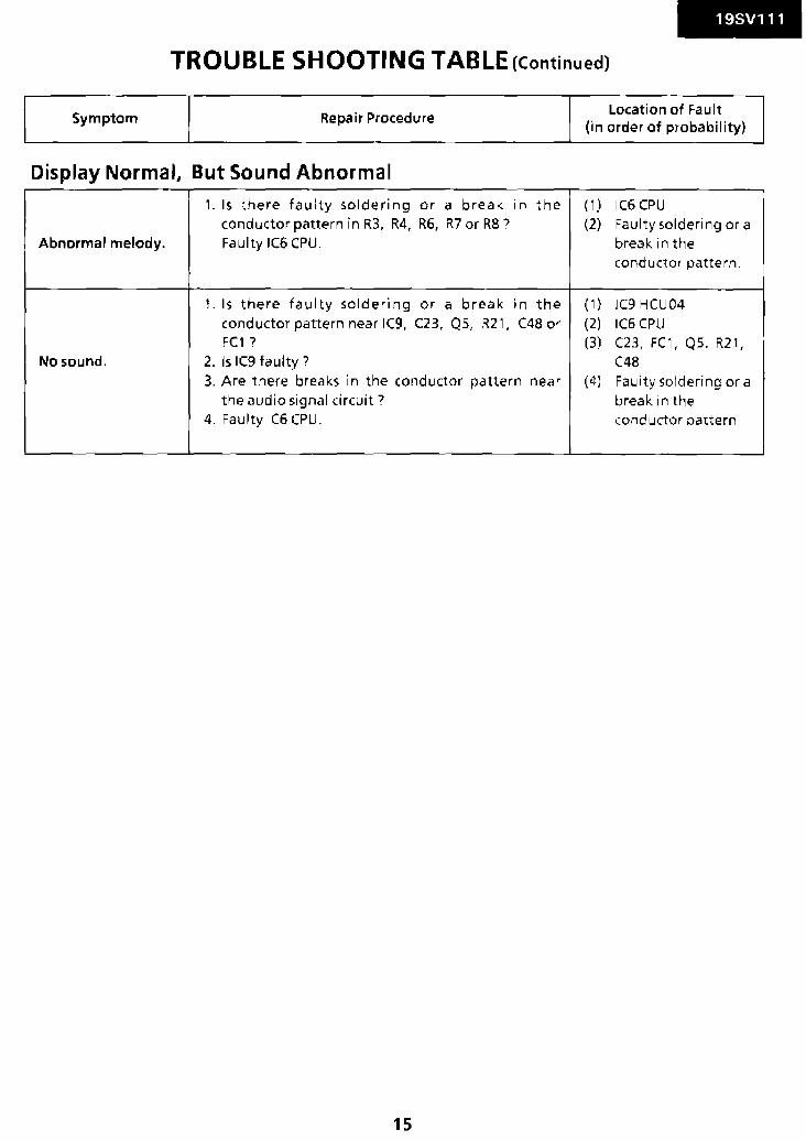
TROUBLE SHOOTING TABLE ccontinued)
Symptom Repair Procedure Location of Fault
(in order of probability)
Display Normal, But Sound Abnormal
1. Is there faulty soldering cr a break in the (1) IC6 CPU conductor pattern in R3, R4, R6, R7 or RS; (2) Faulty soldering or a
Abnormal melody. Faulty IC6 CPU. break in the conductor pattern.
1. Is there faulty soldering or a break in the (1) IC9 HCU04 conductor pattern near IC9, C23, QS, R21, (48 or (2) 1(6 CPU FC1? (3) C23, FC1, QS, R21,
No sound. 2. Is IC9 faulty ? C48 3. Are there breaks in the conductor pattern near (4) Faulty soldering or a
the audio signal circuit? break in the 4. Faulty I C6 CPU. conductor pattern.
15
""
w
_. I I ~
~ I
VI
0'1
J> 0> "
PWB- 9 F4784PE
cCJ~l.A~t • oe~l
~8
~
oe~ o • • 01~
0
PWB-A F507 1 PE
[
SWI IO I SW II02 SW IIOl
SW ti O"'
0'-\.9 0<-00WN
VOl. -uP VOI.-I>Ow>o
' l..J
I
I
SW 1 HJ6 P(IW[R
0 •501
• 1 o oeo o •
•o•~oz
lPZOo ·202
0 0
TPIOOJ-1 004
SW IIO) SW I 101
t5t5r.58 SW1t04 $ W1102
N
I RIC
0 1201 REI:EJV(Q • = 0 O.tll l .tll [I] IC J20 t
I Jc t t>o t ~ 0 I
)t i ~OI
c=J fC tfiOI
T
0
[8
CJ 0· At lOl
:-l(\IE~oJ8 070)
• IC)O o • 0 11103 OlOI
• • O•iOZ 6"~·[ ~ Ra o&
.rr
E - TV•'E~
SWt iOt .AGIPtG c:>
LW6 I S
1 o L•o· • ~107 0 I o• •J oO a
0 1)02 0 401 ..11 0412 •
•• ..c:J J8 • • 7 'LJ 07~ OIJD O • [
0130• Q o lOl 040l 0 c:::::J
I •eo o o?o• •1o2 ~ • R'r70• D 6 ~ ::: : ~·j~[JD
- B SW II OO TVIST01>41G111\C
o~·~ u Rr-4GC
~ ~
'70, TP601·60R
m
PWB- H F6537PE
B PWB- F F6531 PE
[•~ • ~ col 0 102
sw•o•• n 1 nn asw1o2 CHI~~ ~il£S£T
l J
PWB-E F6530PE
[] PWB-D F6529PE
,..
PWB-G F6532PE
~"U oeU
IC7 c:=::J
l:r EA~ TP I02
--[C
c=:J OA 02
• • OJ
c:::::::J I 1~ :
DE IC~ ~ I 8 o
ooO
EcO ICJ lC6
c--~ IC2c=:::J IC •O r.J
c::::::J t!J X2 ocO
• 04
e o~
C\ I
PWB-C F4783PE
065) n,c,5• IC7ll2 LJa u OG51
Je··c) 8~
~
0652 8 T852· 6!l l
~[9 o, I -
OL65<
n ~ l> V\ V\ -V\
~ 0 c .......
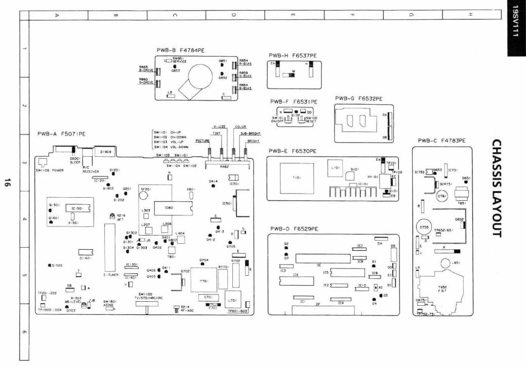
19SV111
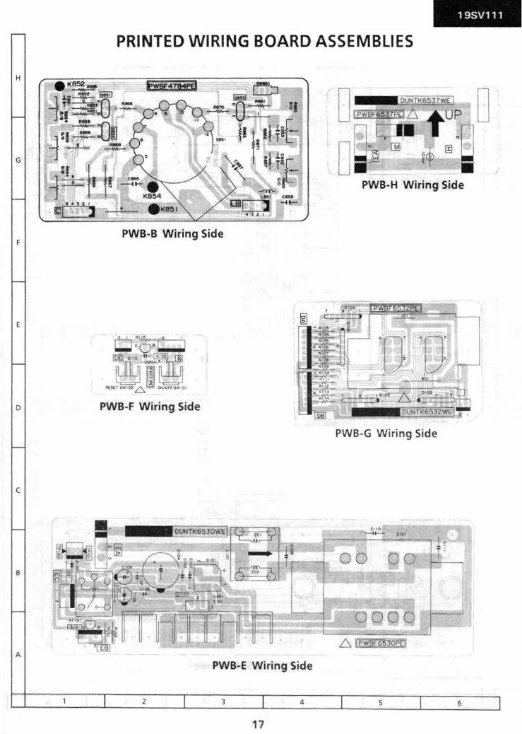
PRINTED WIRING BOARD ASSEMBLIES
H
G
PWB-H W iring Side
F PWB-B Wiring Side
E
D PWB-F Wiring Side
PWB-G Wiring Side
c
00 B
0000
A
PWB-E Wiring Side
2 3 4 5 6
17
19SV111
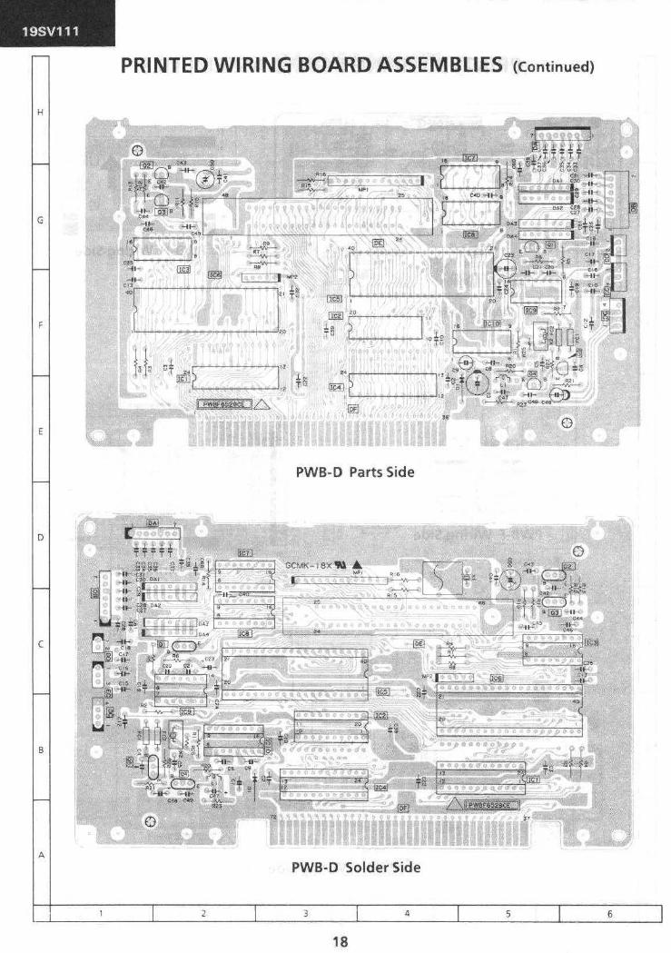
PRINTED WIRING BOA.RD ASSEMBLIES <continued>
H
G
F [1fiD ~~?-~-~
t e. .....:? __,..,..;.,...,.,.,...;.--__.
E
PWB-D Parts Side
D
c
B
A
PWB-D Solder Side
2 3 5 6
18
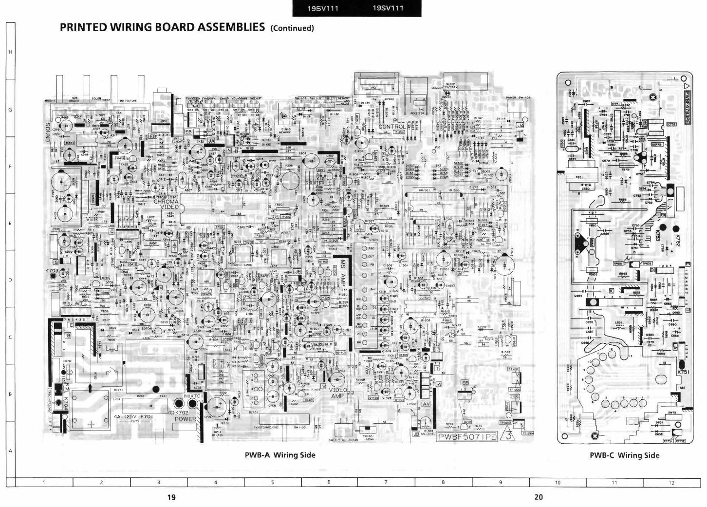
19SV111 19SV111
PRINTED WIRING BOAR.D ASSEMBLIES <continued)
H
-· 0 I>
G I F
E
D
c
B
I 1 A
PWB-A Wiring Side PWB-C Wiring Side
3 4 5 6 7 8 9 10 11 12
19 20
F
E
D
c
B
A
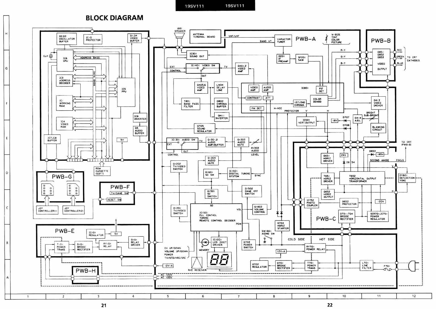
BLOCK DIAGRAM
0
IC3 ~t--LJ\, ~t--rv ~t--~ 1--.~>DORESS t------1
OE:COOER
IC I WORKI NG RAM
IC4 VIDEO R.AM
l i C7.JC8 I BUfFER
- -- PWB-G
_].,
.
--
"' ~ "'
IC!> ..___..__ PPU
r-r-- I v - t-
-LJ-.., !--rv'
f--t- IC9 ~ INVERTER
t--LA j_
0!> J ~
AUDIO BUfFER
:;v L I--
-~~SETTE l ISOI'TI
PWB-F l TV/GAME ~]
~RESET S',\1
H
EXT
CONTROL
19SV111 19SV111
J IC1401 VIOE:O sw
J .r
OUT
0405.6 VIDEO A'JJI' ~
I TV
L404 DELAY LINE
0401,2 VIDEO I-AIII'
BAND VT
AMP AMP
VARACTOR TUNER
10201 IF Pfl(AMP
PWB-A
SF201 SAW
1C801
{
V-SIZE TINT COLOR PICTuRE PWB-8
R-Y
G-Y )I .------t"Hir
9-Y ,I .-:-----i H ;t--
~
08!>1 08!>2 0853
-1 r--) GREEN TO CRT
REO )
~ CATHODES VI0£0 ,I BLUE
H}--
OUTPUT
T801 0802 .__ BANO PASS CHR~A FILTER BUFFER
t--n_ VI0£0 AuDIO
H CONTRAST I ATT - COLOR J IST/2NO LJ OEM()()
~~--t-----------t-r---------~,c~~jl
F- 04 13 VIOE:O ORJVER
EXT
I FM O£T I
y_IN~~+ER JH--------h 0705 SOUND REGIA..ATOR
ICIJOI AuDIO SW TV J 01301,2 rS>-----1~'--1 AUOlO
__( I AMP/SUfFER
_j OUT
01303 AUOIO MUTE
I ./ r/ .____, _ ___, R 1303
AuDIO
CONTROL LEVEL
0 1202 TV/VIDEO SWITCH
0 1201 TV/VIDEO SWITCH
I
01304 AUOIO .WTE
101601 so sw
1 I i
l o•!>OI 1
~ITCH] I so
!CI!'>OI PLL CONTROL T~ING
l
!CI601 OIGJlAL T~ING 1---:---' SYSTEN SYNC
01502 GA.ME Of'F SWITCH
H0180J ~ VOL 1-- VOLUME
CONTROL
R(MOTE CONTROL DECODER Pow t--
SW180•
H- VCC PROTECTOR v H
•
I
-
0707 18V 1---to...._..-,
0708 ....._
0414 A.B.L
-- _.1,
~--
BLA~ING CIRClliT
--~
lO CRT IPWB-81
SECOND ANOOE
06$ 1 HORIZ DRIVER FOCUS
06 54
~--~--~t-1-r~l----~~~ T6$1 T652 lOY60I
r---- HORIZ - HORIZONTAL OUTPUT ---- DEFLECTION --1 I DRIVER TRANSFORME:R YOI(E I
I! 06!2 Ll--_..._ _ _ --+--+---t---jH u I HOR12 OUTPUT
'----;J)--{.H IC7!>2 I .... I PHOTO t------j ~~~~ECTOR t-t-- "i
I 070<4 HOIUZ STARTER
.t-i rJ COUP\..ER
I I
I PWB-C I
07!11-75<4 BRIDGE RECTIFIER
-SCR701,IC751 POWER REGULATOR
PWB-E t
ICIOI REGULA TOR 5 V 1
0 703 ll ~l.-Ab~I-NG_Js_w __ _J ___ c_o_L_D __ S_ID-Ef::-:. j1
::-__ H_O_Tl-S-I_D __ E--i-,---------i 0 10 1 C\ IIC120 1
I 1 Lr RELAY H H J-- \ ·~ J lLEO IOIGIT
POWER It- RY70 I J-SWITCH POWER R£L A'I'
12V- A t-----l__,.. __ _j i rr= ;;~:: := f:!'i::,. H :;:~: J. """ ;"::;.;ro::,_ ,::;;,,J~le:ER!., ~ TV/STO/HRC/IRC
i L------------------1 1~ =' ·-' ~~ATM :r~~IER 1 ~~:: I J PWB-H J [_________________________ --.,-r,..--------:::_0::~~:------------------------------------=-------• I
L70 1
J LINE l F101 I ~------~t-t-------~l~F~IL~T~E~RJ-----C-)~ ~ ' r ~\.y--1
(
l I l--------------~-----------~---------------------------- 1~---~~~-~~:~Q_~·~--------_-_-_-__ -_-_-_-_-__ -_-_-_-_-__ -_-_-_-_-_-__ -_-_-_-__ -_-_-_-_-__ -_-_-_-_-__ -_-_-_-_-__ -_-_-_-__ -_-_-_-_-__ -_-_-_-_-__ -_-_-_-__ -_-_-_-_-__ -_-_-_-_-__ _J __________________________ _ ------------•
2 3 4 5 6 7 8 9 10 1 1 12
21 22
19SV111
BlOCK DIAGRAM (continued)
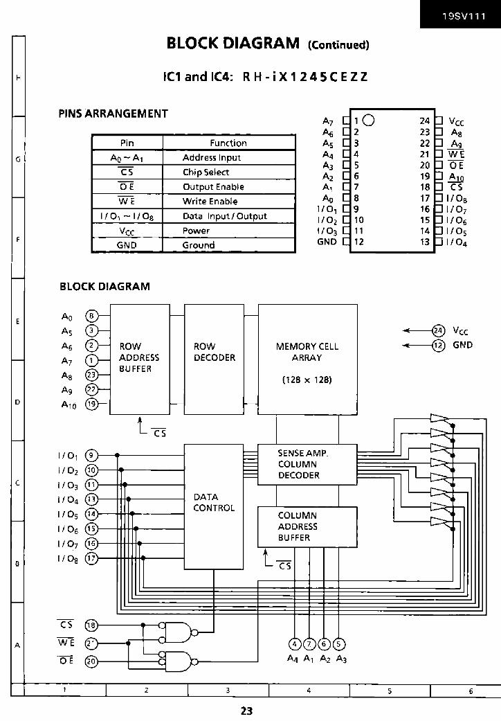
H IC 1 and IC4: R H - i X 1 2 4 5 C E Z Z
PIN_S ARRANGEMENT Az tO 24 Vee A() 2 23 A a
Pin Function As 3 22 Ag
G Ao-A, Address Input
cs Chip Select
A4 4 21 WE A3 5 20 OE A2 6 19 bo
OE Output Enable A, 7 18 cs WE Write Enable Ao 8 17 1/0s
1/01 -l/Oa Data l nput I 0 utput 11 o, 9 16 l/Oz l/02 10 15 l/06
Vee Power 1/03 11 14 l/Os F
GND Ground GND 12 13 l/04
BLOCK DIAGRAM
E Ao
As cv- ~ ~
®--- -+-------@ Vee
A6 ®---- ROW ROW MEMORY CELL ~ GND
Az
As
Ag D A,(j
0- ADDRESS DECODER ARRAY
®-- BUFFER (128 X 128)
CfP-®--- - -
lcs .........
L...-"" 110,
1/02 c 1/03
9 ~ SENSE AMP_ ...... ~ COLUMN
10 ~ """"'~ ~ DECODER
11 ---.....
1/04
1/05
[ /06
13 DATA ~ CONTROL -
~ 14 COLUMN
15 ADDRESS
l/Oz
B r /Oa
16 BUFFER
17 lcs
A
18 }>---J 21 4 7 6 5
20 ~ A4 A, A2 A3
2 3 4 5 6
23
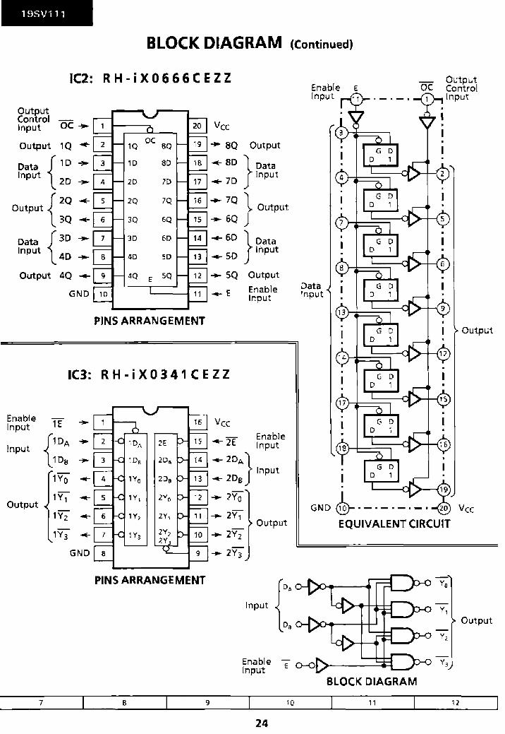
19SV111
BLOCK DIAGRAM (Continued)
IC2: RH-iX0666CEZZ oc Output Enable E Control Input Input
Output Control oc .... Vee Input
Output 1Q +- SQ Output
Data { 10 Input . 20
-so }Data ~ 70 Input
rQ -7Q} Output Output 3Q .... 6Q
Data {3D -+ 60 } Data Input 40 -+50
Input
Output 4Q ~ SQ Output
Enable Data GND Input Input
PINS ARRANGEMENT Output
IC3: R H - i X 0 3 4 1 C E Z Z
Enable 1f ..... Vee Input
fDA .-2f Enable Input Input
1Da .-2DA} 1Yo
Input -+ 2Ds
Output 1~ +- 2Yo
GND ®- ·-·- ·- ·-• 1Y2 +-2Y1
Vee
Output EQUIVALENT CIRCUIT 1Y3 +- 2Y2
PINS ARRANGEMENT Yo
r Input Y,
Da Output
y2
Enable y3 Input
BLOCK DIAGRAM
7 8 9 10 ,, 12
24
19SV111
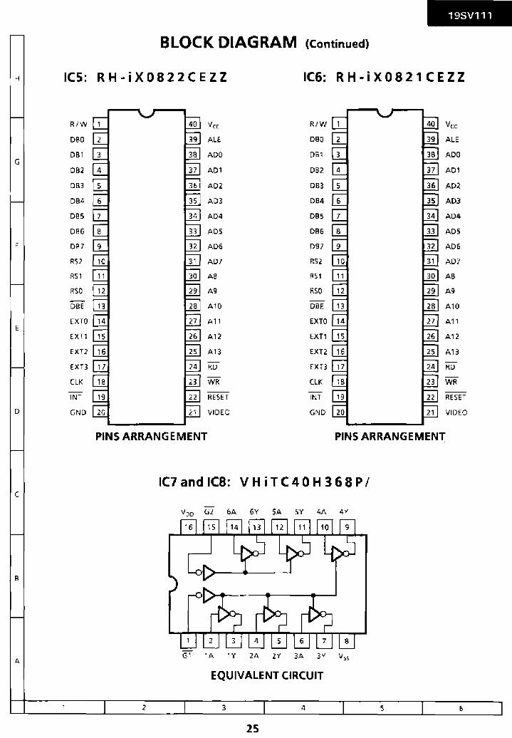
BLOCK DIAGRAM (continued)
H ICS: RH~iX0822CEZZ IC6: R H - i X 0 8 2 1 C E Z Z
Vee Vee
DBO ALE DBO ALE
DB1 ADO DB1 ADO G
D82 AD1 D82 AD1
DB3 AD2 DB3 AD2
DB4 AD3 DB4 AD3
DBS AD4 DBS AD4
DB6 ADS DB6 ADS
f DB7 AD6 DB7 AD6
R52 AD7 R52 AD7
RS1 AB RS1 AB
RSO A9 RSO A9
DBE A10 DBE A10
EXTQ A11 EXTO A11 E
EXT1 A12 EXT1 A12
EXT2 A13 EXT2 A13
EXT3 RD EXT3 RD
CLK WR CLK WR
INT RESET INT RESET
D GND VIDEO GND VIDEO
PINS ARRANGEMENT PINS ARRANGEMEN-r
IC7 and ICB: V H iT C 4 0 H 3 6 8 PI (
VoD G2 6A 6Y SA 5Y 4A 4Y
B
A G1 lA lY 2A 2Y 3A 3Y V 1 ~
EQUIVALENT CIRCUIT
2 3 4 5 6
25
19SV111
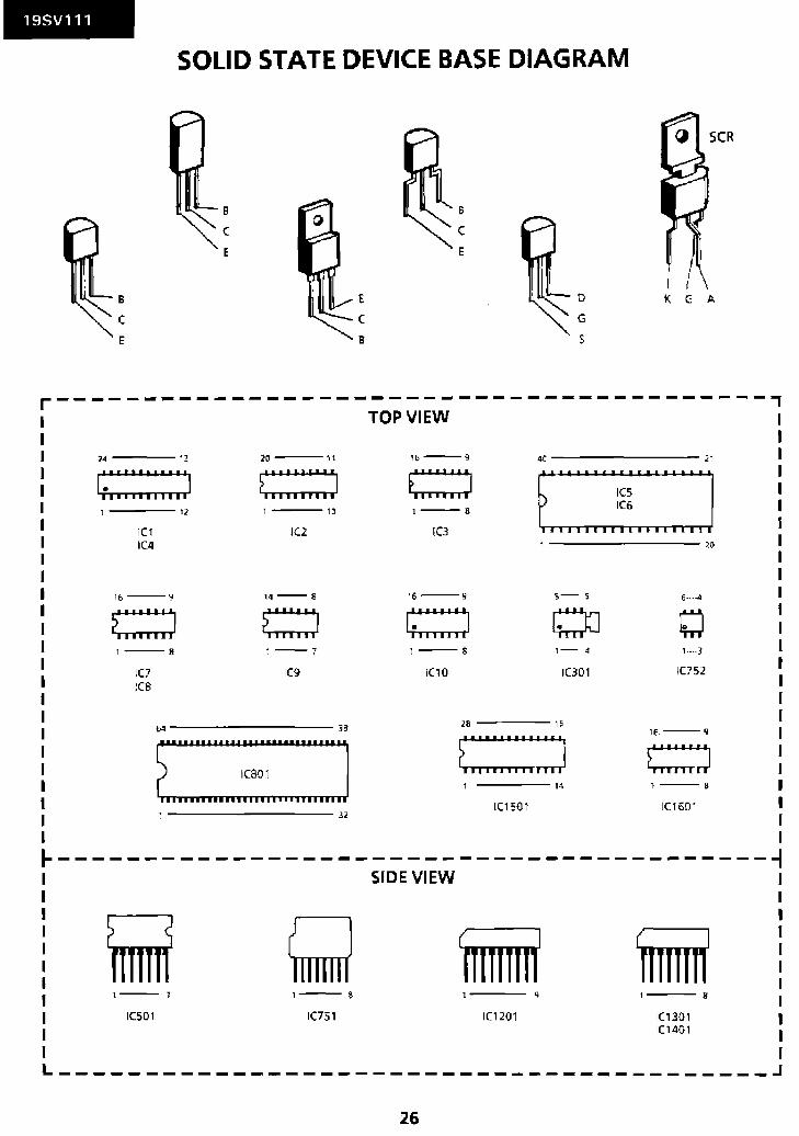
SOLID STATE DEVICE BASE DIAGRAM
B B
c c E E
B E 0 K G A
c c G
E B s
r-----~~--~----~--~----~---------~-----~~-,
~~:::::::::::1 1 1]
1(1 1(4
10 11
c::::::: :I I 10
IC2
16-9 14-8
>::::::::1 a 1-s 1-7
IC7 IC9 1(8
---J·
TOP VIEW
16-9
c::::::1 1-6
ICJ ---~o
16-9 s- s 6----.o1
~~:::::::t 0 0 1-s 1-4 1---3
1(10 IC301 IC752
28 IS
c::::::::::J 16--9
}: ::::: ::I 1 14 1-8
1(1501 1(1601
~-----------------------------------------~ SIDE VIEW I
I I
mmrr: I
1-7 1-8 -g s I ICS01 1(751 1(1201 1C1301 1
1c14o1 I
I L--~-------~-~~-~~---------~~---~--------~~
26

19SV11 1
Memo
27
19SV111
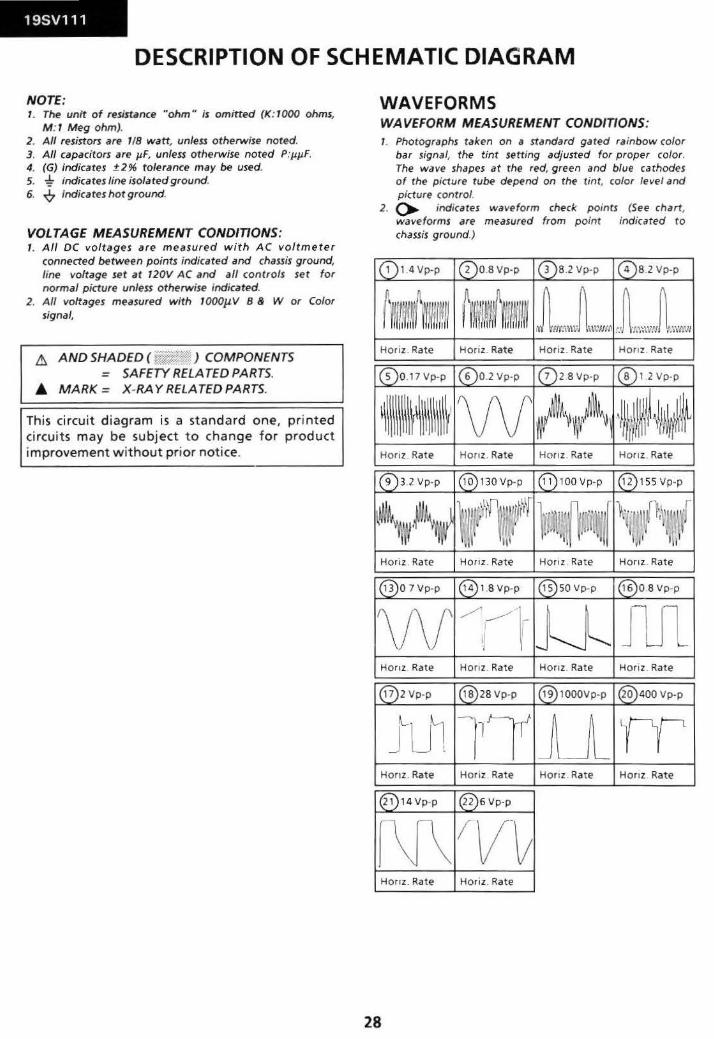
DESCRIPTION OF SCHEMATIC DIAGRAM
NOTE: 7. The unit of resistance .. ohm .. is omitted (K: 1000 ohms,
M: 1 Meg ohm). 2. All resistors are 1/8 watt, unless otherwise noted. 3. All capacitors are pF, unless otherwise noted P:ppF. 4. (G) indicates 1:2% tolerance may be used. 5. .:;. indicates line isolated ground. 6. -Qo indicates hot ground.
VOLTA GE MEA SUREMENT CONDITIONS: 1. All DC voltages are measured with AC voltmeter
connected between points indicated and chassis ground, line voltage set at 120V AC and all controls set for normal picture unless otherwise indicated.
2. All voltages measured with 1000p.V 8 & W or Color signal,
& AND SHADED ( [~~i\\f} ) COMPONENTS = SAFETY RELATED PARTS. .. MARK = X-RAY RELATED PARTS.
This ci rcuit diagram is a standard one, printed ci rcuits may be subject to change for product improvement without prior notice.
WAVEFORMS WAVEFORM MEASUREMENT CONDITIONS: 1. Photographs taken on a standard gated rainbow color
bar signal, the tint setting adjusted for proper color. The wave shapes at the red, green and blue cathodes of the picture tube depend on the tint, color level and picture control.
2. (> indicates waveform check points (See chart, waveforms are measured from point indicated to chassis ground.)
(1) 1.4 Vp-p (2)0.8 Vp-p (3)8.2 Vp· p I ( 4)8.2 Vp-p
{rlltftl!lfmmr!ll tl~~~mllffl JL,t. ,n,,,,.h""" Horiz . Rate Horiz. Rate Horiz. Rate Honz. Rat e
(0o.17 Vp-p (Do.2 vp-p (D2.8 Vp-p 1®1 .2 Vp-p
~~~I Ill\~ \Ill Iii\~ w !~¥~1 ·!!/ill~~·~~~ Horiz. Rate Honz. Rate HOriZ. Rate Horiz. Rate
(9)3.2 Vp-p ~VBovp-p Q0100Vp-p Q~155 Vp-p
~~~~ ~t'fl ;l/f I HI )~~~~~ \l(·~~~~r fi• ,)
Horiz. Rate HOriZ. Rate Horiz. Rate Honz. Rate
@o 7Vp-p @1.8Vp-p '@sovp-p @o.8vp-p
w / ( /lr . I ll M
Honz. Rate Honz. Rate Horiz. Rate Horiz. Rate
@2 Vp-p @28 Vp-p 1@1000Vp-p @400 Vp-p
JLUl l 1lf j_l rr Honz. Rate Horiz. Rat e Horiz. Rate Horiz. Rate
@14Vp-p I Q2)6Vp-p
N\ ~vv Honz. Rate Horiz. Rate
28

H
G
F
E
D
c
B
A
MAIN-2 CIRCUIT
TO
j· .... j· .... ..... · ...... ·-!· ·-rL.
100 ooo ooo 100 •00 ' 00 sea
o•~• I)J ,roo.. turo. 11W
~~~ros = ~ = ~tn ~~«
I CJI~ I~ ,.,,,.
curoo•~ \It·
·".E.> ..... _ ... rr4:: XWOOI!o!.IC 0~...- ~~
l
C: •lO~··
=f· ,.,,,, '·""
~ ··., a sS•• ,,.
~ ..... rT
or!lez UC945Af0 l Z5( t 81~1 G..u.€ OH Sw
.. .., ...
l
•uw a .. oa • H 06 »o no uo
o•lo• l~~·~AlPI 25CI I I$'0AI •1..010 WVT(
(~ . 'fY ! .....
0 l leot T
( l ofO) _ ,, .... v. ua~U•
19SV111 19SV111
This circuit diagram is a standard one, printed circuits may be subject to change for product improvement w ithout prior notice.
,...!10)'
""'
IIIU 104 ... •oHO t1 H S I Q \1. Jftfl • ~ 0~
IH O lhoO$ · i!%0 ....
lhUI .....
'f":f ':f "ff''ft ~ 1:, l ~·It ~~=~~
PWB-A OM11(!.0'11W(V7'1
(2/2)
... ~ """ ..... ..... .. .. 1 rr L f f t i~f l ~ 1 r r f ~·r.:::· • :::::=;.;::;::;:.~::.==,. ....... ==+-.
• •• 0 1 ... "' 11\orf COif t<lU' 7
--- -- - - J ' · ·- -· ... - -- _ ..
Mil Pl. "" ... FM"T cd~l !iiXZ )!
··-t
... .,. ·""'
..... [...... tAI4roJCC
..... "" ._, .. .., . -........ '«,~ [~~
( • • (U
,_ -
--~ ------ ----1
-----·-r -1 ~
~o---------~.~.1 :
-
. .
L--------------------------+--+-----------------------------~------r--i-+--------------------~---------------------< •tv~}---------------~4-+-+---------~"~'~~·~ '""""'
L----------~¥·~
I L-------------------~---------------------------------< • ov)-----------------------~"~M~ ~----~--------------------------------------------------~t+------------------------------------------------------------~r------t--~----------------------------------,1~· · >------------------------------------------U"~~··~
II I I
2
._,,,, ...
3
29
4 5 6 7 8 9 10 11 12
30
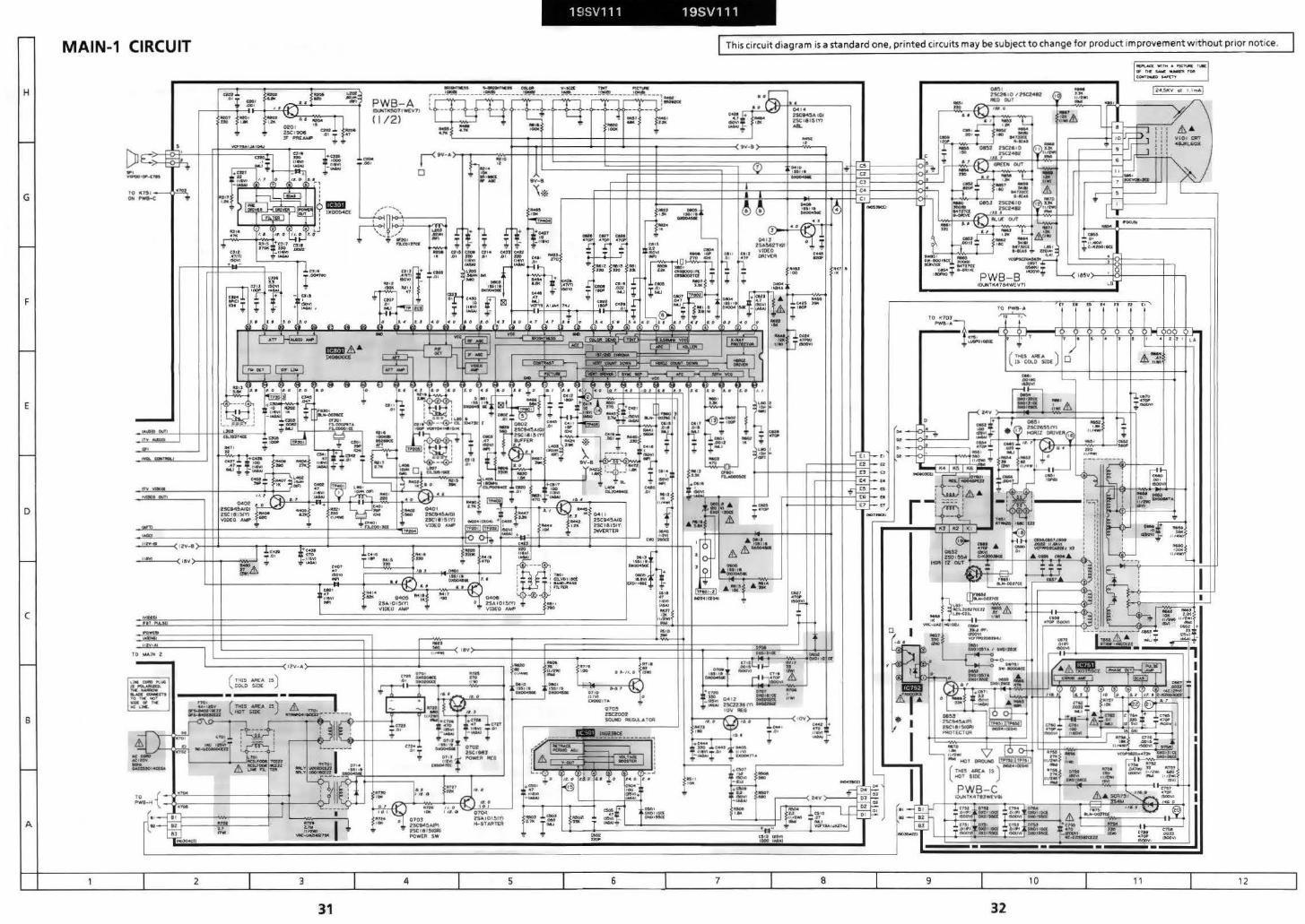
MAIN-1 CIRCUIT
H
G
F
E
D
c
B
A
2 3 4 5
31
H lSV111 19SV111
This circuit diagram is a standard one, .printed circuits may be subject to change for product improvement without prior notice.
6 7 8 9 10
32
IIIIP'\.Atl(wrtlol .t. ~ rc fl' M &MC.......,. ,.CIA CGWT...C $AICTT
12
H
G
E
D
c
B
A
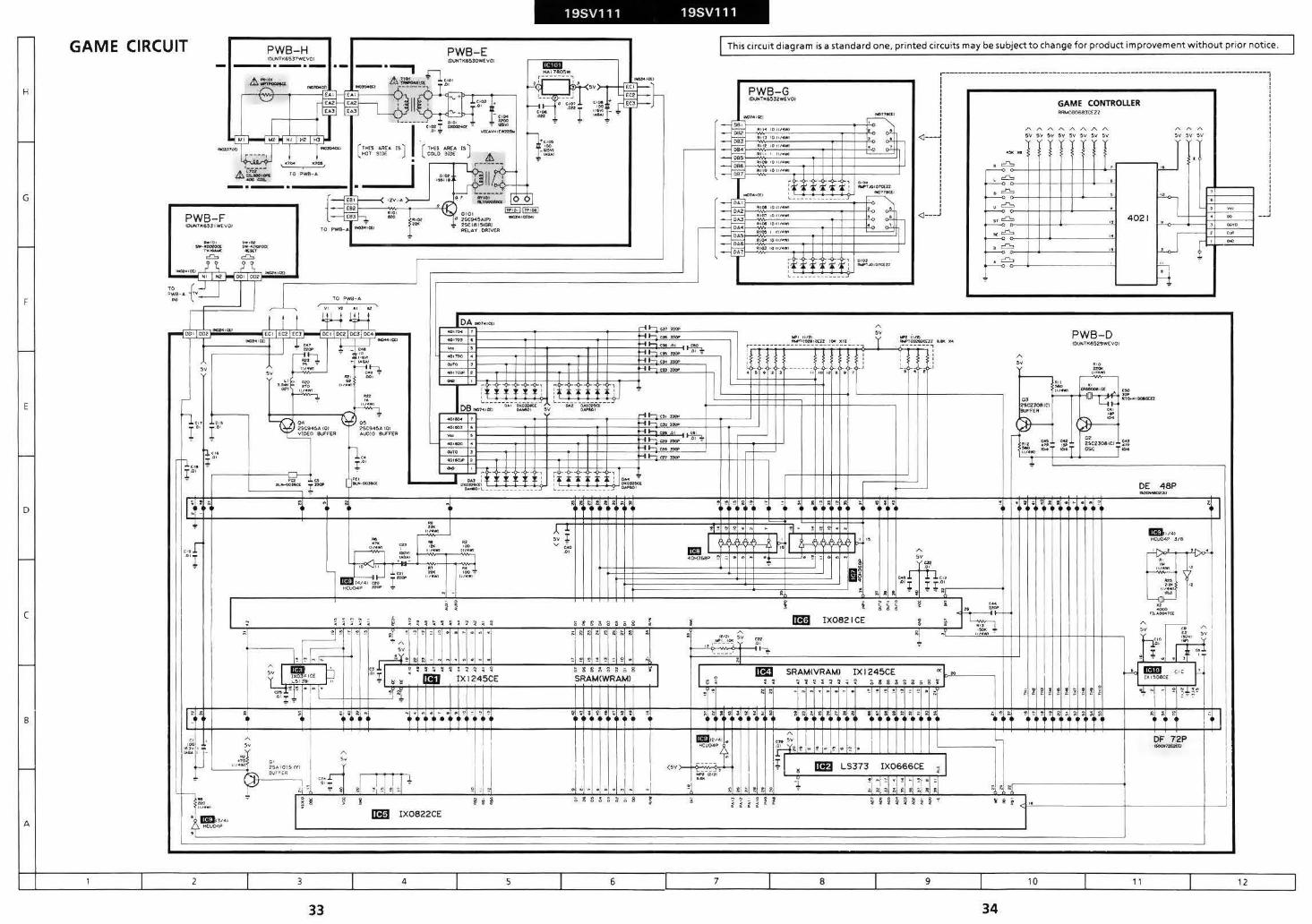
GAME CIRCUIT
h,, r
2
., ~~~ r··
.. "" 1114W'I
PWB-H
3
PWB-E
TO PwO--A
... . . ~ - - -,. T
miiJ IX0822CE
4 5
33
19SV111 19SV111
This circuit diagram is a standard one. printed circuits may be subject to change for product improvement without prior notice.
~gg~ssos
~1 ~ ~ ~ ti ! ~ ~
J! .. ... ~ . ~ssz.aacs
SRAM(WRAMl
.1. .. .. ~ J
6
~ I
(Sv >--k;.,i-:"':"';,.~:>;,.o.....;
-l { ..
7
W 1 +tlb
.----------------------------------------------------------------, f ! II !
GAME CONTROLLER 1
i ~!em ! i l
<-~ ~· ~ ~ ~? ~ 1 H. ~ ;. ~ I
, m; : : ~ .
-'l iJFI.} ~COZS2C'E'Tl .... Xof.
PWB-0
4021 .. _., ""'=----t ""' --t "" - ..j
,--------- -~~C!'..'~!l- !~-~·! -- - , . ·- ~---- , ~'-29wC\tQJ
i IImJ IX0821CE
SRAM(VRAMJ IX1245CE
-1 •
8
I
' I 1 I 1 I
5 .)-; !
"'' .. d
9
w !! ii
10
34
..• -,, .... .,
DE
11
48P
01" 72P <JocH?~
!
12
19SV111
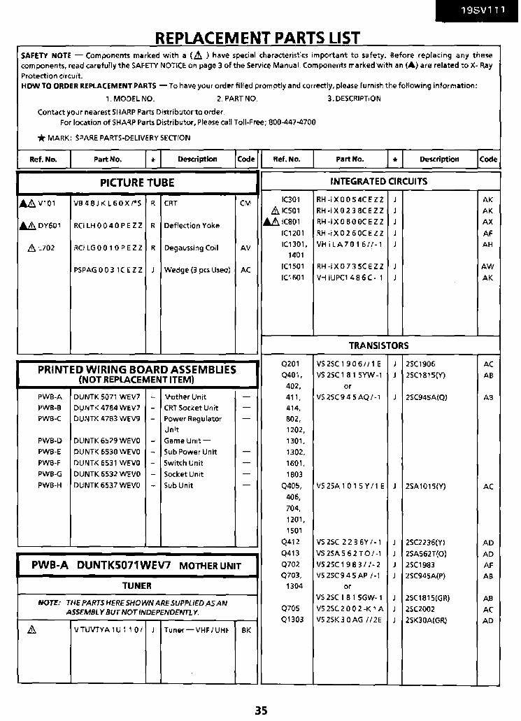
REPLACEMENT PARTS LIST SAFETY NOTE - Components marked with a <.& ) nave special characteristics important to safety. Before replacing any these components, read carefully the SAFETY NOTICE on page 3 of the Service ManuaL Components marked with an (A) are related to X- Ray
Protection circuit. HOW TO ORDER REPLACEMENT PARTS -To have your order filled promptly and correctly, please furnish the following information:
1. MODEL NO. 2. PART NO. 3. DESCRIPTION
Contact your nearest SHARP Parts Distributor to order_
For location of SHARP Parts Distributor, Please call Toll-Free; 800-447-4700
*MARK: SPARE PARTS-DELIVERY SECTION
Ref. No. Part No. * Description Code 'I Ref. No. Part No. * Description Code
PICTURE TUBE INTEGRATED CIRCUITS
A& ViOl VB48JKL60X!*S R CRT CM 1(301 RH -i X 0 0 5 4C E Z Z J AK
6_1C501 RH -i X 0 2 3 8C E Z Z J AK
~DY601 RCi LH 0 0 4 0 P E Z Z R Deflection Yoke £A!C801 RH -iXO 800( E ZZ J AX
1(1201 RH -i X 0 2 6 OC E Z Z J AF
/1).. L702 RCi LG 0 0 1 0 P E Z Z R Degaussing Coil AV 1(1301' VH i l A 7 0 1 611- 1 J AH
1401
PSPAG 0 0 3 1C E Z Z J Wedge (3 pes Used) AC IC1501 RH -i X 0 7 3 SC E Z Z J AW
IC1601 VH iUPC1 4 8 6 C • 1 J AK
TRANSISTORS
Q201 VS 2SC 1 9 0 6/11 E 25(1906 PRINTED WIRING BOARD ASSEMBLIES
J A(
(NOT REPLACEMENT ITEM) Q401, VS 2SC 1 8 1 SYW -1 J 2SC181 5(Y) AB
402, or
PWB-A DUNTK 5071 WEV7 - Mother Unit - 411' VS 2SC 9 4 S AQ 1-1 J 2SC945A(Q) AS PWB-8 DUNTK 4784 WEV7 - CRT Socket Unit - 414,
PWB-C DUNTK 4763 WEV9 - Power Regulato-r - 802,
Unit 1202,
PWB-D DUNTK 6529 WEVO - Game Unit- 1301,
PWB·E DUNTK 6530WEVO - Sub Power Unit - 1302,
PWB-F OUNTK 6531 WEVO - Switch Unit - 1601' PWB-G DUNTK 6532 WEVO - Socket Unit - 1803
PWB-H DU NTK 653 7 WEVO - Sub Unit - Q405, VS 2 SA 1 0 1 5 Y 11 E J 2SA 1015{Y) AC
406,
704,
1201'
1501
Q412 VS 2SC 2 2 3 6Y 1- 1 J 2SC2236(Y) AD
Q413 VS 2SA 56 2 T0/-1 J 2SA562T(O) AD
PWB-A DUNTK5071 WEV7 MOTHER UNIT 0702 VS 2SC 1 9 6 3 I I· 2 J 2SC1963 AF Q703, VS 2SC 9 4 5 AP /-1 J 2SC945A(P) AB
TUNER 1304 or
NOTE: TNE PARTS HERE SHOWN ARE SUPPLIED AS AN VS 2SC 1 8 1 5GW- 1 J 2SC1815(GR) AB
ASSEMBLY BUT NOT INDEPENDENTLY. Q705 VS 2SC 2 0 0 2 -K 1 A J 25(2002 AC Q1303 VS2SK30AG 112E J 2SK30A(GR) AD
A VTUVTYA1U110/ J Tuner-VHF I UHF BK
35
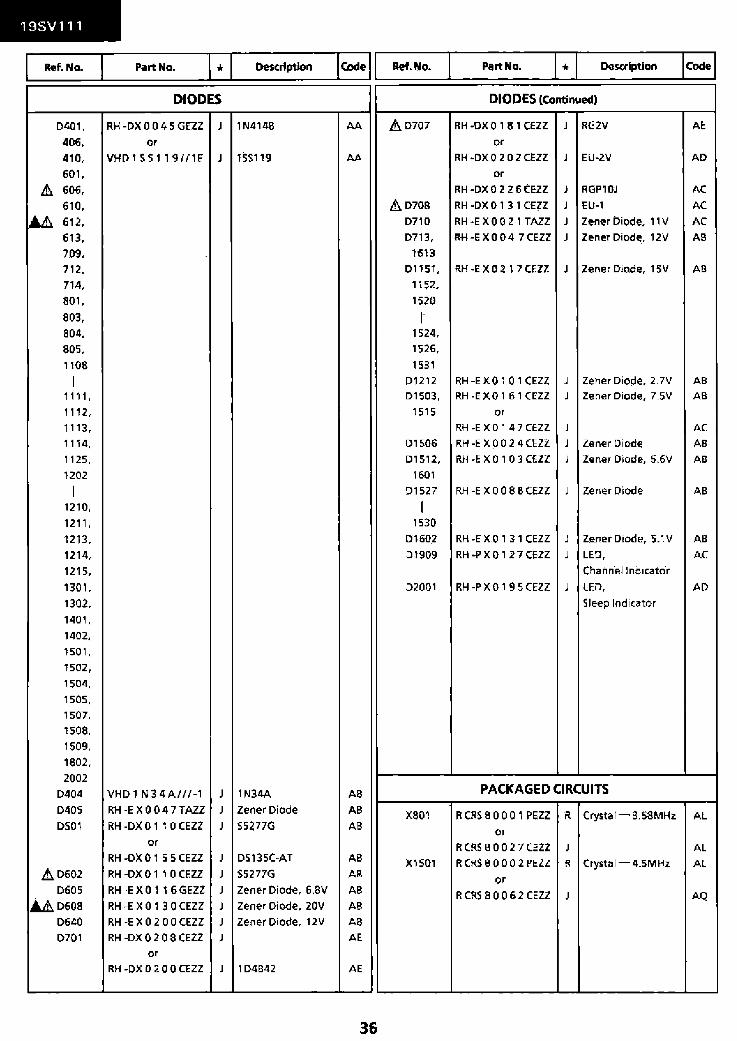
19SV111
Ref. No. Part No. Description I Code II Ref. No. Part No. Description
DIODES DIODES (Continued)
0401, RH -OX 0 0 4 5 GEZZ J 1 N4148 AA blD707 RH -DXO 1 6 1 CEZZ J RGZV AE
406, or or
410, VHD1SS1 19/f1E J 1SS1 19 AA RH -DXO 2 0 2 CEZZ J EU-lV AD
601, or
Al 606, RH -OX 0 2 2 6 (EZZ J AGP10J AC
610, ,1\0708 RH -DXO 1 31 CEZZ J EU-1 AC
A6 612, 0710 RH -E XOO 2 1 TAZ.Z J Zener Oiode. 1 1 v AC
613, 0713, RH-E X004 7 CEll J Zener Diode, 12V AB
709, 1613
712, 01151. RH -E X 0 2 1 7 CEZZ J Zener Diode. 15V AB
714, 1152,
801. 1520.
803, 1-804. 1524,
805, 1526,
1108 1531
I 01212 RH -E X 0 1 0 1 (EZZ J Zener Diode. 2.7V AB
1 1 1 1' 01503, RH -E X 0 1 6 1 (EZZ J ze ner Diode. 7 .5V AB
1 112, 1515 or
1113, RH -E X 0 1 4 7 CEZZ J AC
1114, 01506 RH -EX 0 0 2 4 CEZZ J Zener Diode AS
1125, 01512. Rf.l -E X 0 1 0 3 CEZZ J Zener Diode, 5.6V AB
1202 1601
I 01527 RH -EX 0 0 8 6 CEZZ J Zener Diode AB
1210. I 1211' 1530
1213, Dl60.2 RH -E XO 1 3 1 CEZZ J Zener Diode, 5.1V AB
1214, 01909 RH -P X 0 1 2 7 CEll J LED, AC
1215, Channel indicator
1301, 02001 RH -P X 0 1 9 5 CEZZ J LED, AD
1302, Sleep Indicator
1401.
1402,
1501.
1502,
1504,
1505,
1507,
1508,
1509,
1802,
2002
0404 VHD 1 N 3 4A//f-1 J 1N34A AB PACKAGED CIRCUITS
D405 RH -EX 004 7 TAZZ J Zener Diode AB X801 R CAS 8 0 0 01 PEZZ R Crystal- 3. SSM Hz AL 0501 RH -OX 0 1 1 0 CEZZ J 55277G AB or
or R CRS B 0 0 2 7 CEZZ J AL RH -DX 0 1 5 SCEZZ J D5135C-AT AB X1501 R CAS 80 0 0 2 PEZZ R Crysta I - 4-SM H:l AL
/lD602 RH -OX 0 1 1 0 CEZZ J S5277G AB or
0605 RH -E X 0 1 1 6 GEZZ J ZenerDiode, 6.8V AB R CAS 8 0 0 6.2 CEZZ J AQ ~0608 RH -E X 0 1 3 0 CEZZ J Zener Diode, 20V AB
0640 RH -EX 0 2 0 0 CEZZ J Zener Diode, 12 v AB
0701 RH -DXO 2 0 8CEZZ J AE
or
RH -OX 0 2 0 OCEZZ J 104842 AE
36

19SV111
Ref. No. Part No. Description I Code Jl Ref. No. Part No. lleKription
COILS CAPACITORS
L202, VP .- R F R-8 2 K 0000 j 0.82].!H AS (209, VCEAGA 1 CW33 7M j 330 16V AC
203 317, Electrolytic
L205 VP -MKR 5 6 MOOQO J 0.56].!H AB 319,
L206 RC i L i 04 7 3 CEZZ J PIF Detector AD 432,
L207 RCili0510CEZZ J AFT AF 444,
L303 RC i L i 0 3 7 4 CEZZ J Sound Detector AD 1204,
L40 1, VP -X F 1 0 0 K 0000 J 10JJH AB 1308,
601, 1616
1201' C335. VCEAGA 1 CW 1 OBM J 1000 16V AD
1501, Electrolytic
1502. (407, VCE 9AA 10N4 76M J 47 16V {N.P) AC
1601 801 Electrolytic
L402 VP -X F 1 5 0 K 0000 J 15JJH AB (418, VCE 9AA 1 HW1 OSM J 1 50V (N.P) AB
L403 VP- 0 F 1 2 1 K 0000 J 1 20].!H AC 614 Electrolytic
L404 R C i L Z 0 4 9 4 CEZZ J Delay Line AH (423, VCEAGA 1CW227M J 220 16V AC
L405 R C i L P 0 0 9 4 CEZZ J 18{)MHz Filter AB 1609 Electrolytic
L406, VP-MK 1 OOKOOOO J 10']lH AB (424, vee SPA 2Hl470 K J 47p soov AA 602 1601 Ceramic
,11L701 R C i L F 0 0 8 7 CEZZ J Line Filter AL (438, VCEAGA 1 CN477M J 470 16V AC
or 442 Electrolytic
R C i L F 0 0 8 8 CEZZ J AK (504 VCEAGA 1 VW1 07M J 100 35V AC
L1503 VP- X F 1 0 1 K 0000 J 100]lH AB Electrolytic
I (505 VCEAGA 1 VW4 76M J 47 35V AB
1508 Electrolytic
(512 VCEAGA 1EW108M J 1000 25V AD
Electrolytic
FILTERS (627, VCK YPA 2H-B 4 71 K J 470p soov AA
719 Ceramic SF201 R F i l C 0 1 3 7 CEZZ J Surface Acoustic AH ,11C701 RC- QZ 0 2 0 DCEZZ J 0.1 AC125V AE
We~veFilter UL Spec
CF301 RFiLC0029TAZZ J Sound Take-Off AD C712 VCK YPA 2HB 152 K J 0.0015 soov AA or
Ceramic R F i l C 0 0 0 1 CEZZ J AE C720 VCEAGA1 EW337M J 330 2SV AC
CF401 RF i L C 0 (} 1 3 CEZZ J 4.5MHz Trap AE Electrolytic
CF601 R F i LA 0 0 0 5 CEZZ J 503kHz AF C726 VCEAGA 1 VW477M J 470 35V AD
Electrolytic
TRANSFORMERS (803 VCE9 AA 1 HW47 4M J 0.47 50V (N.P) AC
Electrolytic .&_ T701 R TRN P 0 4 1 6 CEZZ J Power Transformer AV C815 VCE9 AA 1 HW22 SM J 2.2 50V (N.P) AB
T801 R C i l V 0 1 1 8 CEZZ J Band Pass Filter AD Electrolytic
C817, VCEAGA 1 CWl 07M J 100 16V AB
1319, E I ectrol.yt ic
CONTROLS 1803
(1502 VCEAGA 1 AW33 7M J :no 10V AB R214 RVR- B 5 1 9 8 CEZZ J 10k(B) RF-AGC AC
Electrolytic R216 RVR - B 5 2 6 9 CEZZ ) 100k{8}AFT AB
R462 RVR - B 5 2 9 2 CEZZ J 1 Ok{B) Brightness/ AK
10k(B} Sub-BrightJ
10k(B) Color/
1k{8) Vert. Size/
10k{B) Tint/
1 Ok{B) Picture
R1303 RVR - B 5 2 6 5 CEZZ J 1 Ok(B) Audro Level AB
37
19SV111
Ref. No. Part No. Description I Code II Ref. No. Part No. Description
RESISTOkS PWB-B DUNTK4784WI!!V7 CRT SOCK_ET UNIT
,& R448 VRS -VV 3AB 1 2 3 J J 12k 1W AA TRANSISTORS Oxide Film
/A R480 VRS -VV 3 LB 2 7 0 J J 27 3W AB Q851, VS2SC 2 4 8 2 I I - 1 J 25(2482 AD
Oxide Film 852, or
.6,&. R_614 VRD-RA 2 BB9 3 J J 39k 1/BW Carbon AA 853 VS2SC2610/-1E J 2SC21510 AD
A&_R615 VRD-RA 2 BE 1 2 3 J J 121r. 1/BW Carbon AA
.6.& R616 VRD-RA 2 BE 56 2 J J 5.6k 1/SW Carbon AA
A&_ R622 .VRD-RA2BE1 53J J 15k 1/8W Carbon AA
.&, R702 VRW-KV3NC 2 R 7 K J 2-7 7W Cement AC COIL
_.& R706 VRN-VV 3 AB_1 RO J J 1 lW AA L851 VP - L K 2 2 1 K 0000 J 220j.lH AC Metal Coating
AR717 VRS -VV 3 LB 3 3 0 J J 33 3W AB
OKide Film
R718 VRS -VV 3LB 8 2 0 J J 82 3W AB CONTROLS Oxide Film
R725 VRS -VV 3 AB 2 7 1 J J 270 1W AA R854 RVR·B 4 7 3 2 CEZZ J 5k{B) Red Bias, AC
Oxide Film 859, Green Bia,s,
_&, R729 VRC-UAZHG 2 7 5 K J 2.7M 112W Solid AA 864 Blue Bias
A R1607 VRS -VV 308 27 3 J J 27k 2W AA R860, RVR- B 4 7 2 7 CEZZ J 300(8) Green Drive, AC
Oxide Film 865 Blue Drive
_&.R1615 VR$-VV3DB 151 J J 150 2W AA Oxide Film
RR1501 RM PTC 0 1 2 8 CEZZ J 22k:x7 AB CAPACITORS Resistor Array
RR1502, RM PTC 0 1 3 5 CEZZ J 22kx4 AB cess RC-K ZOO 1 6CEZZ J 0.01 1.4kV Ceramic AC
1503 Resistor Array C857 VCQ PSC 2 GA 563K J 0.056 400V AB
Polypro Film
SWITCHES AND RELAY RESISTORS
SW1100 QSW -5 0 0 6 2 CEZZ J TV I STD I HRC I IRC AG A RB67, VRS- VU 3AB 123 J J 12k.1W Oxide Film AA
SW1101, QSW -K 0 0 1 4 CEZZ J Channel Up, AC .&.. 869,
1102, Channel Dowen, 6 871
1103. Volume Up,
1104 Volume Dowon
SW1106 QSW-KO 0 2 OCEZZ J Power AD SW1801 QSW -8 0 0 0 6 CEZZ J Aging AC SWITCH
.&_ RY701 RR l YU 0 0 2 0 CEZZ J Power Relay AK SW851 QS.W -B 0 0 1 S CEZZ J Service {Cut-off} AC or
RR L YU 0 0 1 8 CEZZ J Al
MISCELLANEOUS PARTS MISCELLANEOUS PART
.&_ F701 QFS • B 4 0 2 3 CEZZ J Fuse -4A 12 5V AC AC 5851 Q$0CV 0 9 1 3CEZZ J Socket-CRT AK
or
QFS-84021 GEZZ J AD
QFSHD1002CEZZ J Fuse Holder AA
-F701 (2 used)
FB301, R B LN • 0 0 3 6CEZZ J Ferrite Bead AB
603
RRMCU 0 1 7 7 CEZZ J Remote Control AN
or Receiver
RRMCU 0 1 5 3 CEZZ J AR
38
19SV111 I
Ref No . Part No. 1•1 Description jcode jj Ref. No. Part No. I• I Desuiptlon
PWB-C DUNTK4783WEV9 POWER REG. UNIT CAPACITORS
C653 VCEAG.A.1 EW 107M J 100 25V AD INTEGRA TED CIRCUITS
Electrolytic
.&&,1C751 AH- i X 0 3 59 CEZZ J AL ~C656, VCF PPD 3CA 222 J J 0 .00221.6kV AD
.&..!h_IC752 AH -F XO 0 03 CEZZ J AK ~ 657, Metalized Potyster
A& 65S
C659, VCK YPA2HB 471 K J 470p soov AA
757, Ceramic
759, TRANSISTORS 760,
VS2SC2655Y/-1 J 2SC2655 AE 765 0651
C660 VCK YPA 2HB 1 02 K J 0.001 500V AA .6.0652 VS 2SD 1 5 5 4 //1 E J 2SD1554 AL
Ceramic Q653 VS 2SC94 5 AP /-1 J 25C945A(P} AS
C661 VCQ PSB 2 JA 102 K J 0.001 630V AB or
Polypro Film VS 2SC 1 8 1 5 GW-1 j 2SC181 5(GR) AB
C664 VCF PPD 2 DB 394 J J 0.39 200V AE
Metalized Polyster
.t:b, C667 RC- KZOO 3 OCEZZ J 0.0033AC1 25V AD
Ceramic
DIODES ~C66S VCEAAA2EW 106M J 10 250V AD
Electrolytic .&_ D651, RH -DX 0 1 0 5 TAZZ J TVR1J AD liC669 RC • K Z 0 0 3 B CEZZ J 470p 2k.V AS .&. 652 or Ceramic
RH -DX 0 1 3 2 CEZZ J EU-1A AC C670 VCK YPU 2HS 471 K J 470p SOOV AA ,AD653 RH -OXOO 8 6 TAZZ J RH1S AC Ceramic .&. D654 RH -OX 0 1 3 2 CEZZ J EU·1A AC C672, VCK YPS 2HE 103 P J 0.01 soov AS
or 751 Ceramic RH -OX 0 1 2 6 CEZZ J TVR1G(TP) AC I
or 754 RH -OX 0 1 3 1 CEZZ J EU-1 AC .!hC755 RC • E Z 0 0 8 2 CEZZ j 470 200V AQ
0655 RH -DX 0 1 2 6 CEZZ J TVRlG(TP) AC Electrolytic .&.0751 RH -DX 0 1 1 0 CEZZ J S5277G AS (756 VCQ PS82DA473 K J 0.047 200V AB
1 or Polypro Film .&. 0754 RH -OX 0 1 5 SCEZZ J DS135C-AT AB (758 VCK YPA 2HB 332 K J 0.0033500V AB .&.0755 RH -E X 0 1 0 6 CEZZ J Zener Diode, 82V AS Ceramic &. 0756 RH -DXO 1 3 1 CEZZ J EU-1 AC ,&C761 VCEAAH2CW 107M J 100 160V AE
or Electrolytic RH -DX 0 1 2 6 CEZZ J TVR1G(TP} AC ~C763 VCQYSH 1 HM 103 K J 0.01 sov AA
.A.&, SCR751 VHS 354M I ILB1 E J Silicon Controlled AK Mylar Rectifier (764 VCEAGA 1 EW 337M J 330 25V AC
Electrolytic
C776 VCK YPA 2HB 152 K J 0.0015500V AA
Ceramic
COIL
L651 R C i L Z 0 5 2 7 CEZZ J Linearity Coi I AF
TRANSFORMERS
A_ T651 RTRN Z 0 1 6 8 CEZZ J Hori:rontal Driver AH
A,A T652 R TAN F 1 4 B 2 CEZZ J Horizontal Output BD
39
19SV111
Ref. No. Part No. Description I code II Ref. No. Part No. Description
RESISTORS TRANSISTORS
R654 VRS - W 3 LB 3 9 0 J J 39 3W AB Q1 VS 2SA 1 0 1 S Y /-1 J 2.SA101S(Y) AC
OxideFiim Q2, VS 2SC2 3 OS C/-1 J 2SC2308 AB
JS::.. R655 VRN- VV 3ABR 3-3 J J 0.33 1W AA 3 Metal Coating 04. VS 25(94 5 AQ 1-1 J 2SC945A(Q) AB
,& R656, VRN - W 3AB 1 R 0 J J 1 lW AA 5
ih 661 Metel Coating
&_ R657 VRS - VV 3DB 3 3 1 J J 330 2W AA Oxide Film
,£. R658 VRS - SV 2HC 1 0 0 J J 10 1/2W AA
FR Oxide Film
6. R662 VRS-SV2HC103J J 10k 112W AA DIODES
FROxide Film DA1. RH -DX 0 3 2 6 CEZZ J Diode Array AK
Jh R664 VRN- VV 3ABR 4 7 J J 0.47 1W AA 3 Met<~ I Coating DA2, RH -OX 03 2 5 CEZZ J Diode Array AK
,&& R665 VRD- RA 2BE 6 8 3 J J 68k 11SW AA 4 Carbon
&£ R666 VRD- RA 2BE 4 7 3 J J 47k 1/BW AA
Carbon
.&, R754 VRS - VV 3 LB 3 3 1 J J 330 3W AB
Oxide Film
,& R759 VRS- SV 2 HC 1 51 J J 150 1/.2W AA PACKAGED CIRCUIT FROxide Film
X1 RCRS B 0 0 8 1 CEZZ J Crystal AH
X2 R F i LA 0 0 4 7 CEZZ J AG
MPl RMPTC 0 2 8 1 CEZZ J Resistor Array AE
MP2 RMPTC 0 2 8 2 CEZZ J Resistor Array AC
SWITCH
SW751 QSW- B 0 0 0 6 CEZZ J Horiz. Centering AC
MISCELLANEOUS PARTS COIL
FB651, R 8 L N- 0 0 3 7 CEZZ J Ferrite Bead AB L1 VP- X F 3 R 3 K 0000 J 3.3lJH AB
652,
751
CAPACITORS
(1 VCEAGAOJW 107M J 100 6.3V AA
PWB-D DUNTK6529WEVO GAME UNIT (9 VCE 9AA 1 HW 225M
Electrolytic
J 2.2 SOV (N.P) AS
INTEGRA TED CIRCUITS cso RTO-H 1 008CEZZ J
Electrolytic
Trimmer, 30p AC
IC1, RH - i X 1 2 4 5 CEZZ J AP 4
1(2 RH- i x o 6 6 6 crzz J AL
IC3 RH - i X 0 3 4 1 CEll J AF
ICS RH - i X 0 8 2 2 CEZZ J AZ.
IC6 RH- i X 0 8 2 1 CEZZ J AY
IC7, VH iTC 40 H 3 6 8 P I J AK MISCELLANEOUS PARTS
8 FC1, RBLN- 0 0 3 6 CEZZ J Ferrite Bead AB IC9 VH iTCHCU 0 4 P -1 J AE 2 IC10 RH- i X 1 50 B CEZZ J AL
40
19SV111
Ref. No. Part No. I * I Description [code [[ Ref. No. Part No. [ * I Description
PWB-E DUNTK6530WEVO SUB POWER UNIT PWB-F DUNTK6531 WEVO SWITCH UNIT
INTEGRA TED CIRCUIT SWITCHES
IC101 VH i HA 17805 W- 1 J AD SW101, QSW -K 0 0 2 0 CEZZ J TV/GAME, AD 102 RESET
TRANSISTOR
Q101 VS2SC 9 4 5 A P I -1 J 2SC94SA(P) AB
or
V525C 1 81 5 GW-1 J 25C1815{GR) AB
PWB-G DUNTK6532WEVO SOCKET UNIT
DIODES DIODES
0101 RH -DX 0 3 2 4 CEZZ J AC D103, R MPT J 0 1 0 7 CEZZ J Zener Diode Array AE 0102 VHD155119//-1 J 155119 AB 104
SOCKET
CAPACITORS QSOCN 0 7 7 8 CEZZ J Socket AF
C104 VCE AVH 1 EN 228M J 2200 2SV AE (GCJme Controller)
Electrolytic
C10S VCEAGA 1EW107M J 100 25V AD
Electrolytic PWB-H DUNTK6537WEVO SUB UNIT C108 VCE AGA 1 CW1 07M J 100 16V AB
Electrolytic
,&_PR101 RMPTP 0 0 2 6 CEZZ J Positive Coefficient AF
Thermistor
TRANSFORMER
,1lT101 RTRNP 0 4 8 1 CEZZ J Power AX
RELAY
,& RY101 MISCELLANEOUS PARTS
RRL YU 0 0 2 2 CEZZ J PowerReray AH
VSP 0 010 P- E 78S J Speaker- 8 ohm AU
.&.. Q ACC D30 14 CESA J AC Line Cord AH
Q TAN Z 0326 CEZZ J Antenna Terminal AS
Board
R RMCG 0684 CESA J lnfrCJred Remote BX
Control Unit
R RMCG 0683 CESA J Game Controller AX {2 pes)
41
19SV111
Ref. No. Part No. Description I code II Ref. No. Part No. Description
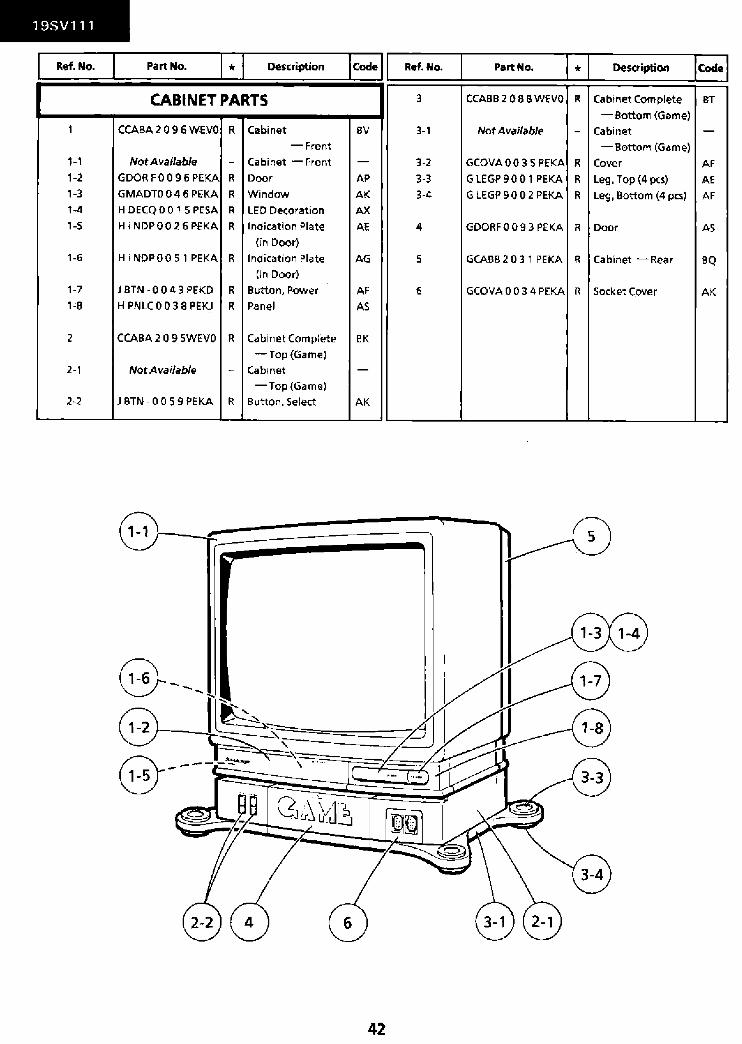
CABINET PARTS 3 CCABB 2 0 8 B WEVO R Cabinet Complete BT
-Bottom {Game) 1 CCABA 2 0 9 6 WEVO R Cabinet BV 3-1 Not Available - Cabinet -
-Front -Bottom (Game)
1-1 Not Available - Cabinet -Front - 3-2 GCOVAOO 3 5 PEKA R Cov-er AF 1-2 GDOR FO 0 96 PEKA R Door AP 3-3 G LEGP 9 0 0 1 PEKA R Leg. Top {4 pes) AE 1-3 GMADTO 0 4 6 PEKA R Window AK 3-4 G LEGP 900 2 PEKA R Leg, Bottom (4 pes) AF 1-4 H DECQ 0 0 1 5 PESA R LED Decoration AX
1-S Hi NDPOO 2 6 PEKA R Indication Plate A"E 4 GDORF 0 0 9 3 PEKA R Door AS On Door)
1-6 Hi NDPOO 51 PEKA R Indication f>late AG 5 GCABB 2 0 3 1 PEKA R Cabinet -Rear BQ (In Door)
1-7 j BTN - 0 0 4 3 PEKD R Button, Power AF 6 GCOVA 0 0 3 4 PEKA R Socket Cover AK ,,a H PNLCOO 3 8 PEKj R Panel AS
2 CCABA 2 0 9 5WEVO R Cabinet Complete BK
-Top(Game)
2-1 Not Available - Cabinet --Top{Game)
2-2 j BTN- 0 0 59 PEKA R Button, Select AK
42

19SV111
Ref. No. Part No. Description
RRMCG0683CE SA GAME CONTROLLER
1 9SJ56-6106·C J Controller Cabinet. AL
Top (WI Controller
Overlay)
2 95156-7578-C J Controller Cab1net, AE
Bottom
3 95J56-7579-A J Control Pad AC
Actuator
4 95J56-0899-B J AlB Button AA
Actuator
5 95156-7598-C J Controller Cable AX
(W/7P Plug)
6 95J56-0900-A J AJB Button Contact AD
7 95J56-8233-C J Control Pad .O..E
Contact
8 95156-8235-A J Select/Start Contact AC
9 9 5 J 5 6-W326-A J Screw, 2x8 AA
43
19SV111
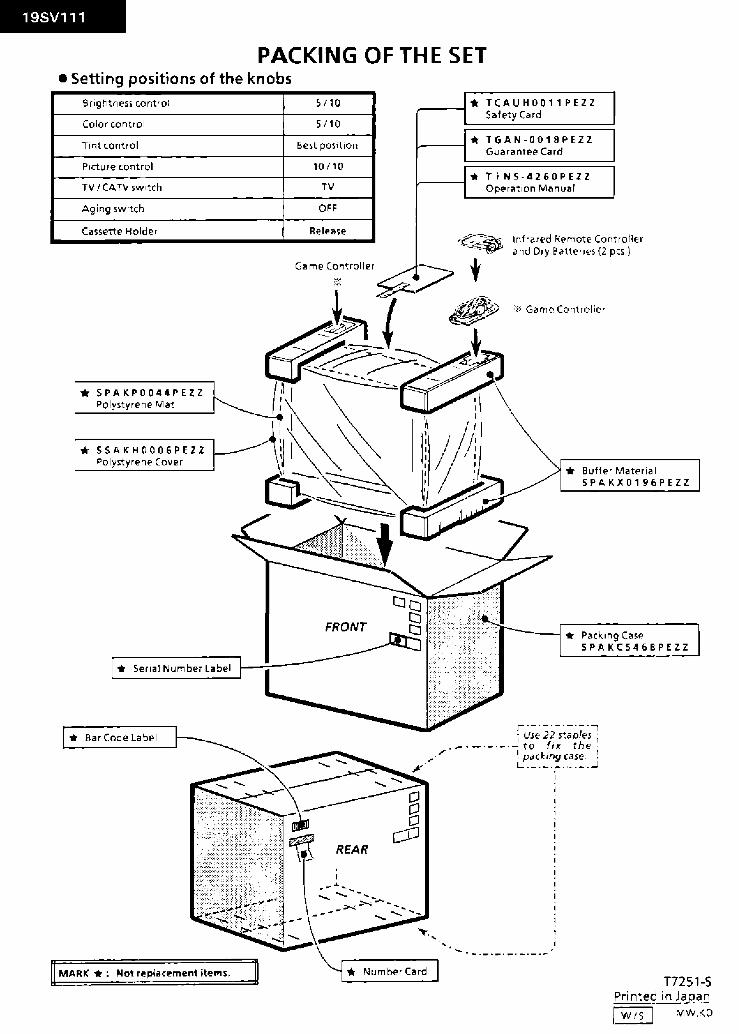
PACKING OF THE SET • Setting positions of the knobs
Brightness control
Color control
Tint control
Poctu1e cont1ol
TV I CATV swotch
Aging switch
Cassette Holder
* SPAKP0044PEZZ Polystyrene Ma~
* SSAKH0006PElZ Polystyrene Cover
* Serial Number Label
* Bar Code Label
II MARK *: Not replacement items. II
s 110
5/10
Best position
10/10
TV
OFF
Relea~e
Game Controller
REAR
......... -...... ........ ........ .... ...
.-----1* TCAUH0011PEZZ Salety Card
1.----1* TGAN-001BPEZZ Guarantee Card
~---1* T i NS-4Z60PEZZ Operation Manual
,.~ ":._~
t
--~-·-·-/"
Infrared Remote Controller and Dry Batter1es (2 pes.)
:'il Game Controller
* Butler M<~teri<ll SPAKX0196PEZZ
* Packmg Cas!' SPAKC546BPEZZ
r ·-· -·- ·-·- ·--, ; Use 22 staples ;
-to fix the · ~ packing case. ! L ·-·-·-· ·-·- . ..I
;;....::~ .......... -_..-"""_ ........................ ...
..... ..... _. ________ ,...
Number Card T7251-S
Printed in Japan ~ MW.KD