Embed Size (px)
Citation preview
Results in Physics 6 (2016) 879–883
Contents lists available at ScienceDirect
Results in Physics
journal homepage: www.journals .e lsevier .com/resul ts - in-physics
Gate dielectric strength dependent performance of CNT MOSFET andCNT TFET: A tight binding study
http://dx.doi.org/10.1016/j.rinp.2016.11.0022211-3797/� 2016 The Authors. Published by Elsevier B.V.This is an open access article under the CC BY-NC-ND license (http://creativecommons.org/licenses/by-nc-nd/4.0/).
⇑ Corresponding author.E-mail address: [email protected] (Md. Shamim Sarker).
Md. Shamim Sarker ⇑, Muhammad Mainul Islam, Md. Nur Kutubul Alam, Md. Rafiqul IslamDepartment of Electrical and Electronic Engineering, Khulna University of Engineering & Technology, Khulna 9203, Bangladesh
a r t i c l e i n f o a b s t r a c t
Article history:Received 8 September 2016Received in revised form 23 October 2016Accepted 1 November 2016Available online 4 November 2016
Keywords:CNT TFETSubthreshold slopBarrier width, Conduction band (C.B) andValance band (V.B)Oxide dielectric strengthTight binding approach
This paper presents a comparative study between CNT MOSFET and CNT TFET taking into account of dif-ferent dielectric strength of gate oxide materials. Here we have studied the transfer characteristics, on/offcurrent (ION/IOFF) ratio and subthreshold slope of the device using Non Equilibrium Greens Function(NEGF) formalism in tight binding frameworks. The results are obtained by solving the NEGF andPoisson’s equation self-consistently in NanoTCADViDES environment and found that the ON state perfor-mance of CNT MOSFET and CNT TFET have significant dependency on the dielectric strength of the gateoxide materials. The figure of merits of the devices also demonstrates that the CNT TFET is promising forhigh-speed and low-power logic applications.
� 2016 The Authors. Published by Elsevier B.V. This is an open access article under the CC BY-NC-NDlicense (http://creativecommons.org/licenses/by-nc-nd/4.0/).
Introduction
Silicon oriented CMOS technology are very much popular insemiconductor industries due to their extraordinary matured pro-cess technology and low cost. However, when the existing CMOStechnology enters into nanometer regime (below 100 nm) thistechnology hits a plateau [1]. This is because in this scaling limit,the semiconductor industry faces some serious problem regardingthe fabrication process and some adverse size effect includingshort channel effects, parasitic capacitance, and leakage currentsetc., and these effects become more severe when gate length isscaled continuously [2,3]. In recent years, extensive researcheshave been carrying out to explore new materials and as well asnew technology to replace the existing CMOS technology and sup-press its drawbacks. Tunneling field effect transistor (TFET), whichworks on the basis of band to band tunneling are drawing massattention due to their lower subthreshold slop and low off stateleakage current [4–10]. Since the basis of operation of TFET is bandto band tunneling, TFET is more immune to short channel effectsthan its MOSFET counterpart [11–13]. However, in spite of severaladvantages of TFET over conventional MOSFET, TFET suffers from aserious problem to overcome, which is its low ON state current dueto presence of tunneling barrier. Existing Si-based TFET devicesprovides very low ON current [14], it is therefore very much impor-
tant to search proper material system for TFET. Carbon nanotubehas a potential to be the appropriate channel material to replaceSi in this new technology due to its unique quasi one dimensionalproperty such as high electron mobility and high Fermi velocity[15]. Since the tunneling transistor is a new type of device, it isof utmost important to explore the performance of this device withdifferent parameters.
It is to be noted here that the conventional scaling rule of MOS-FET (which is constant electric field) is not blindly followed to scaledown the TFET. In a previous study Bhuwalka, et al. [16] haveexplained about the rule of scaling down of Si TFET and concludedthat constant field scaling rule is not applicable for TFET, thoughthey have some works where the channel length and oxide thick-ness are decreased simultaneously [11,16], following the Den-nard’s scaling rule [17]. However, when studying TFET, it is moreconvenient to vary one parameter at a time, in order to get com-plete understanding of the effect of each change and isolate theeffect.
In this article we report the gate-oxide dielectric strengthdependent performance comparison for CNTMOSFET and CNTTFETconsidering double gate structure. We have shown that the effectof different high-k dielectrics is not similar in these two cases.The physics behind their dissimilar behavior is also explained withtheir respective band diagram and electric field. The currentvoltage (I-V) characteristics are obtained by solving the NEGFand Poisson’s equation self-consistently in NanoTCADViDESenvironment. Other performances of the device like ION/IOFF ratio
880 Md. Shamim Sarker et al. / Results in Physics 6 (2016) 879–883
and subthreshold slope are studied from the transfer characteris-tics in conjunction with band diagram.
This article is organized as follows: device structure and simu-lation methods are explained under section II, while section IIIdemonstrate the details results and discussion, and section IV con-tains the summery.
Simulation details
Device structure
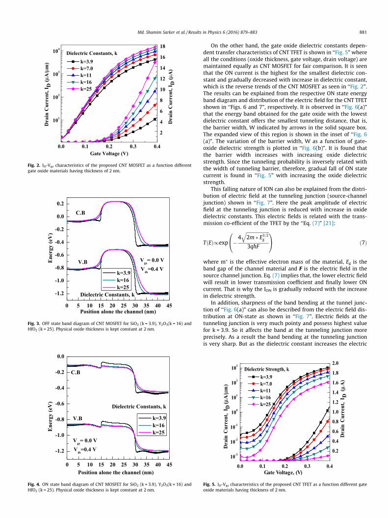
The double gate device structure used in our simulation isshown in ‘‘Fig. 1”. We have used CNT in the channel of the deviceswith chirality of (13,0), having a length of 15 nm. CNT in this chi-rality has a band gap of 0.75 eV. Source and drain are the extensionof the channel doped with n-type dopant for the MOSFET. For theTFET source is doped with p-type while the drain is doped with n-type dopant. The doping density of the source and drain reservoirsis taken f ¼ 5� 10�3. On the top and bottom of the channel weused gate insulator that is extended over the source, and drain aswell. For suppressing the ambipolar conduction in TFET, weapplied a small body bias in the bottom gate and it is also appliedfor MOSFET for fair comparison between them.
Simulation approach
The transfer characteristics of CNT MOSFET and TFET are deter-mined by solving Schrodinger equation using NEGF formalism,which are solved self consistently with 3-D Poison’s equation.The 3D Poison’s equation is given by [18,19]
r½eð~rÞr/ð~rÞ� ¼ �q½pð~rÞ � nð~rÞ þ NþDð~rÞ � Nþ
A ð~rÞ þ qfix� ð1Þ
where /ð~rÞ is the electrostatic potential, eð~rÞ is the dielectric con-stant, Nþ
D and NþA are the concentration of ionized donors and accep-
tors, respectively, and qfix is the fixed charge. Remaining terms arethe electron and hole concentration, nð~rÞ and pð~rÞ, respectively.These are evaluated by solving the Schrodinger equation using openboundary condition considering the tight binding Hamiltonian withan atomistic (pz)basis.
The greens function can be expressed as [12,13]
GðEÞ ¼ ½EI � H � RS � RD��1 ð2Þ
where ‘E’ is the energy, ‘I’ the identity matrix, ‘H’ is the Hamiltonianof the GNR written in tight binding approach and RS and RD are theself-energies of source and drain contacts, respectively. Here trans-port is assumed completely ballistic and charge is considered aspoint charge.
Assuming that the chemical potential of the reservoirs arealigned at equilibrium with the Fermi level of the GNR, and given
Source reservoirs
CNT Channel
Drain reservoirs
Dielectric
Bottom Gate
Dielectric
Top gate15 nm 15 nm
15 nm
Fig. 1. Proposed CNT MOSFET/CNT TFETstructure.
that there is no confined states. The electron and hole concentra-tions in the channel are
nð~rÞ ¼ 2Z þ1
Ei
dE½jwSðE;~rÞj2f ðE� EFSÞ þ jwDðE;~rÞj2f ðE� EFDÞ� ð3Þ
and
pð~rÞ ¼ 2Z Ei
1dEf½jwSðE;~rÞj2½1� f ðE� EFSÞ� þ jwDðE;~rÞj2½1� f ðE� EFDÞ�g
ð4ÞHere ‘~r’ is the coordinate of carbon site, ‘f ’ is the Fermi-Dirac
occupation factor, and jwSj2ðorjwDj2Þ is the probability that statesinjected by the source (or drain) reach the carbon site (~r) andEFSðorEFDÞ is the Fermi level of the source (or drain)
The current is computed by
I ¼ 2qh
Z þ1
�1dETðEÞ½f ðE� EFSÞ � f ðE� EFDÞ� ð5Þ
where ‘q’ is the electron charge, ‘h’ is the planks constant and ‘T(E)’is the transmission coefficient that is given as-
T ¼ �Tr
XS
�Xþs
!GXD
�XþD
!Gþ
" #ð6Þ
Here Tr is the trace operator. The simulation is carried out attemperature 300 K.
Result and discussion
The dielectric materials used in our study are listed in ‘‘Table 1”along with their dielectric constants:
As the attempt to compare the performance between the CNTMOSFET and CNT TFET, we first present the oxide dielectricstrength dependent transfer characteristics of the CNT MOSFETshown in ‘‘Fig. 2”, where the thickness of the gate insulator isassumed as 2 nm. The results are evaluated varying the gate biasVgs from 0 to 0.4 V, while keeping the drain bias Vds fixed at0.4 V. The curves is plotted in logarithmic and as well as linearscale to understand the difference between ION and IOFF clearly.
From ‘‘Fig. 2” it is seen that the ON current is the lowest for thesmallest dielectric strength and gradually increases with increasein dielectric strength although the variation of OFF current is neg-ligible. These results can be explained from the respective ON stateand OFF state band diagram shown in ‘‘Figs. 3 and 4”. It is seen in‘‘Fig. 3” that the magnitude of barrier height for both low-K andhigh-K gate dielectric are almost similar. That means the channelis equally resistive for electron to flow for both cases. As a resultthe variation of OFF state current is almost negligible. While inON state, ‘‘Fig. 4” shows that high-K gate oxide paves the lowerenergy path for electron. As a result ON state current for high-Kgate oxide become higher than the low-K gate oxide and theseobservation is consistent with the results reported by other groupsas well [20].
Table 1Lists of dielectric materials with their dielectric strengths.
Dielectric material Dielectric strength
Silicon dioxide (SiO2) 3.9Silicon nitride (Si3N4) 7.0Hafnium silicate (HfSiO4) 11Yttrium Oxide (Y2O3) 16Hafmium oxide (HfO2) 25
0.0 0.1 0.2 0.3 0.4
101
102
103
104
Dra
in C
urre
nt,I
D(
Aµ)
Dielectric Constants, kD
rain
Cur
rent
,ID
(A
/mµ
µ)
Gate Voltage (V)
k=3.9 k=7.0 k=11 k=16 k=25
2
4
6
8
10
12
14
16
18
Fig. 2. ID-Vgs characteristics of the proposed CNT MOSFET as a function differentgate oxide materials having thickness of 2 nm.
0 5 10 15 20 25 30 35 40 45
-1.2
-1.0
-0.8
-0.6
-0.4
-0.2
0.0
0.2
Dielectric Constants, k
C.B
V.B Vgs
= 0.0 VV
ds=0.4 V
Ene
rgy
(eV
)
Position alone the channel (nm)
k=3.9 k=16 k=25
Fig. 3. OFF state band diagram of CNT MOSFET for SiO2 (k = 3.9), Y2O3(k = 16) andHfO2 (k = 25). Physical oxide thickness is kept constant at 2 nm.
0 5 10 15 20 25 30 35 40 45
-1.2
-1.0
-0.8
-0.6
-0.4
-0.2
0.0
Position alone the channel (nm)
Ene
rgy
(eV
)
C.B
V.B
Dielectric Constants, k
k=3.9 k=16 k=25
Vgs
= 0.0 VV
ds=0.4 V
Fig. 4. ON state band diagram of CNT MOSFET for SiO2 (k = 3.9), Y2O3(k = 16) andHfO2 (k = 25). Physical oxide thickness is kept constant at 2 nm.
Md. Shamim Sarker et al. / Results in Physics 6 (2016) 879–883 881
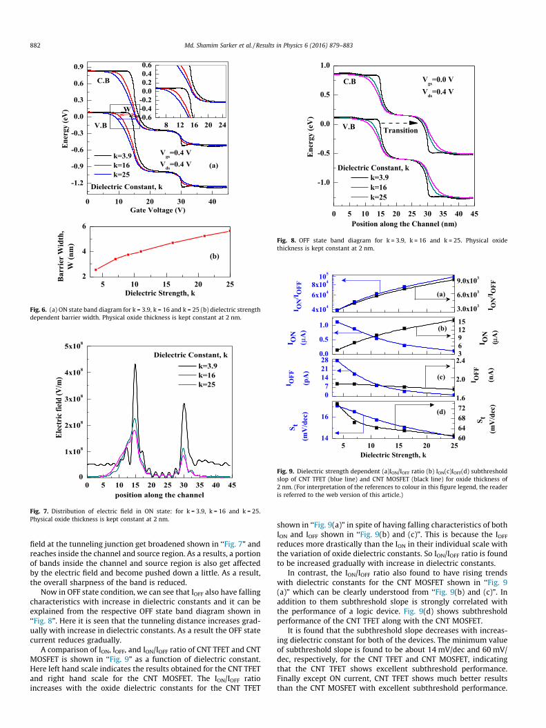
On the other hand, the gate oxide dielectric constants depen-dent transfer characteristics of CNT TFET is shown in ‘‘Fig. 5” whereall the conditions (oxide thickness, gate voltage, drain voltage) aremaintained equally as CNT MOSFET for fair comparison. It is seenthat the ON current is the highest for the smallest dielectric con-stant and gradually decreased with increase in dielectric constant,which is the reverse trends of the CNT MOSFET as seen in ‘‘Fig. 2”.The results can be explained from the respective ON state energyband diagram and distribution of the electric field for the CNT TFETshown in ‘‘Figs. 6 and 7”, respectively. It is observed in ‘‘Fig. 6(a)”that the energy band obtained for the gate oxide with the lowestdielectric constant offers the smallest tunneling distance, that is,the barrier width, W indicated by arrows in the solid square box.The expanded view of this region is shown in the inset of ‘‘Fig. 6(a)”. The variation of the barrier width, W as a function of gate-oxide dielectric strength is plotted in ‘‘Fig. 6(b)”. It is found thatthe barrier width increases with increasing oxide dielectricstrength. Since the tunneling probability is inversely related withthe width of tunneling barrier, therefore, gradual fall of ON statecurrent is found in ‘‘Fig. 5” with increasing the oxide dielectricstrength.
This falling nature of ION can also be explained from the distri-bution of electric field at the tunneling junction (source-channeljunction) shown in ‘‘Fig. 7”. Here the peak amplitude of electricfield at the tunneling junction is reduced with increase in oxidedielectric constants. This electric fields is related with the trans-mission co-efficient of the TFET by the ‘‘Eq. (7)” [21]:
TðEÞ1exp �4
ffiffiffiffiffiffiffiffiffiffiffiffiffiffiffiffiffiffiffiffi2m � E3=2
g
q3q�hF
0@
1A ð7Þ
where m⁄ is the effective electron mass of the material, Eg is theband gap of the channel material and F is the electric field in thesource channel junction. Eq. (7) implies that, the lower electric fieldwill result in lower transmission coefficient and finally lower ONcurrent. That is why the ION is gradually reduced with the increasein dielectric strength.
In addition, sharpness of the band bending at the tunnel junc-tion of ‘‘Fig. 6(a)” can also be described from the electric field dis-tribution at ON-state as shown in ‘‘Fig. 7”. Electric fields at thetunneling junction is very much pointy and possess highest valuefor k = 3.9. So it affects the band at the tunneling junction moreprecisely. As a result the band bending at the tunneling junctionis very sharp. But as the dielectric constant increases the electric
0.0 0.1 0.2 0.3 0.4
10-3
10-2
10-1
100
101
102
103
Dra
inC
urre
nt,
I D(
A)
Dielectric Strength, k
Dra
inC
urre
nt,
I D(
A/
m µ
µ
µ)
Gate Voltage, (V)
k=3.9k=7.0k=11k=16k=25
0.2
0.4
0.6
0.8
1.0
1.2
1.4
1.6
1.8
2.0
Fig. 5. ID-Vgs characteristics of the proposed CNT TFET as a function different gateoxide materials having thickness of 2 nm.
0 10 20 30 40
-1.2
-0.9
-0.6
-0.3
0.0
0.3
0.6
0.9
8 12 16 20 24-0.6-0.4-0.20.00.20.40.6
Vgs
=0.4 VV
ds=0.4 V (a)
W
C.B
V.B
Dielectric Constant, k
Ener
gy (e
V)
Gate Voltage (V)
k=3.9 k=16 k=25
5 10 15 20 252
4
6
(b)
Bar
rier
Wid
th,
W(n
m)
Dielectric Strength, k
Fig. 6. (a) ON state band diagram for k = 3.9, k = 16 and k = 25 (b) dielectric strengthdependent barrier width. Physical oxide thickness is kept constant at 2 nm.
0 5 10 15 20 25 30 35 40 450
1x10⁸
2x10⁸
3x10⁸
4x10⁸
5x10⁸
Dielectric Constant, k
Elec
tric
field
(V/m
)
position along the channel
k=3.9 k=16 k=25
Fig. 7. Distribution of electric field in ON state: for k = 3.9, k = 16 and k = 25.Physical oxide thickness is kept constant at 2 nm.
0 5 10 15 20 25 30 35 40 45
-1.0
-0.5
0.0
0.5
1.0
Vgs
=0.0 VV
ds=0.4 V
V.B
C.B
Dielectric Constant, k
Transition
Ene
rgy
(eV
)
Position along the Channel (nm)
k=3.9 k=16 k=25
Fig. 8. OFF state band diagram for k = 3.9, k = 16 and k = 25. Physical oxidethickness is kept constant at 2 nm.
0.0
0.5
1.0
07
142128
4x10⁴
6x1048x104
105
5 10 15 20 2514
16
(b)
(c)
(d)
(a)
I ON
(Aµ
)
I OFF
(nA
)S t
(mV
/dec
)
S t(m
V/d
ec)
I ON
/IO
FF
I ON
/IO
FFI O
FF
(pA
)
I ON
(Aµ
)
Dielectric Strength, k
3691215
1.6
2.0
2.4
3.0x10³
6.0x10³
9.0x10³
60646872
Fig. 9. Dielectric strength dependent (a)ION/IOFF ratio (b) ION(c)IOFF(d) subthresholdslop of CNT TFET (blue line) and CNT MOSFET (black line) for oxide thickness of2 nm. (For interpretation of the references to colour in this figure legend, the readeris referred to the web version of this article.)
882 Md. Shamim Sarker et al. / Results in Physics 6 (2016) 879–883
field at the tunneling junction get broadened shown in ‘‘Fig. 7” andreaches inside the channel and source region. As a results, a portionof bands inside the channel and source region is also get affectedby the electric field and become pushed down a little. As a result,the overall sharpness of the band is reduced.
Now in OFF state condition, we can see that IOFF also have fallingcharacteristics with increase in dielectric constants and it can beexplained from the respective OFF state band diagram shown in‘‘Fig. 8”. Here it is seen that the tunneling distance increases grad-ually with increase in dielectric constants. As a result the OFF statecurrent reduces gradually.
A comparison of ION, IOFF, and ION/IOFF ratio of CNT TFET and CNTMOSFET is shown in ‘‘Fig. 9” as a function of dielectric constant.Here left hand scale indicates the results obtained for the CNT TFETand right hand scale for the CNT MOSFET. The ION/IOFF ratioincreases with the oxide dielectric constants for the CNT TFET
shown in ‘‘Fig. 9(a)” in spite of having falling characteristics of bothION and IOFF shown in ‘‘Fig. 9(b) and (c)”. This is because the IOFFreduces more drastically than the ION in their individual scale withthe variation of oxide dielectric constants. So ION/IOFF ratio is foundto be increased gradually with increase in dielectric constants.
In contrast, the ION/IOFF ratio also found to have rising trendswith dielectric constants for the CNT MOSFET shown in ‘‘Fig. 9(a)” which can be clearly understood from ‘‘Fig. 9(b) and (c)”. Inaddition to them subthreshold slope is strongly correlated withthe performance of a logic device. Fig. 9(d) shows subthresholdperformance of the CNT TFET along with the CNT MOSFET.
It is found that the subthreshold slope decreases with increas-ing dielectric constant for both of the devices. The minimum valueof subthreshold slope is found to be about 14 mV/dec and 60 mV/dec, respectively, for the CNT TFET and CNT MOSFET, indicatingthat the CNT TFET shows excellent subthreshold performance.Finally except ON current, CNT TFET shows much better resultsthan the CNT MOSFET with excellent subthreshold performance.

Md. Shamim Sarker et al. / Results in Physics 6 (2016) 879–883 883
But this low ON current also has an advantage in switching andlow power application.
Conclusion
Oxide dielectric strength dependent performance is studied fordouble gate CNT MOSFET and CNT TFET. The ON current perfor-mance of CNT MOSFET improves with increase in oxide dielectricconstants, but in case of TFET this performance deteriorates. TheOFF state current decreases with increasing dielectric constantfor the CNT TFET, although it is almost constants for the CNT MOS-FET. The ION/IOFF ratio and the subthreshold performance of bothdevices improve with increase in dielectric constants. Our studydemonstrates that except ON current, TFET has much better per-formance than MOSFET in other performance parameters andseems to be a potential candidate for high-speed and low-powerswitching devices.
Appendix A. Supplementary data
Supplementary data associated with this article can be found, inthe online version, at http://dx.doi.org/10.1016/j.rinp.2016.11.002.
References
[1] Assad F, Ren Z, Vasileska D, Datta S, Lundstrom M. On the performance limitsfor Si MOSFETs: a theoretical study. IEEE Trans Electron Devices 2000;47(1):232–40.
[2] Nur Kutubul Alam Md, Shaffatul Islam Muhammad, Golam Kibria Md, RafiqulIslam Md. Anomalous staircase CV characteristics of InGaSb-on-Insulator FET.IEEE Trans Electron Devices 2014;61(11):3910–3.
[3] Celler GK, Cristoloveanu S. Frontiers of silicon-on-insulator. J Appl Phys2003;93(9):4955–78.
[4] Seabaugh AC, Zhang Q. Low voltage tunnel transistor for beyond CMOS logic.Proc IEEE 2010;98(12):2095–110.
[5] Ionescu AM, Riel H. Tunnel field effect transistor as energy efficient electronicswitches. Nature 2011;479(7373):329–37.
[6] Ionescu AM, de Michielis L, Dagtekin N, Slavator G, Cao J, Rashu A, Bartsch S.Ultra low power: emerging device and their benefits for integrated circuits.IEDM Tech Dig 2011. 16.1.1–16.1.4.
[7] Bhuwalka KK, Sedlmair S, Ludsteck AK, Tolksdorf C, Schulze J, Eisele I. Verticaltunnel field effect transistor. IEEE Trans Electron Devices 2004;51(2):279–81.
[8] Choi WY, G park B, Lee JD, Liu TJK. Tunneling field effect transistor (TFETs) withsubthreshold swing (SS) less than 60 mV/dec. IEEE Electron Device Lett.2007;28(8):743–5.
[9] Boucart K, Ionescu AM. Double gate tunnel FET with high K dielectric. IEEETrans Electron Devices 2007;54(7):1725–33.
[10] Ghosh B, Akram MW. Junctionless tunnel field effect transistor. IEEE ElectronDevice Lett 2013;34(5):584–6.
[11] Bhuwalka KK, Schulze J, Eisele I. Scaling the vertical tunnel field effecttransistor with tunnel bandgap modulation and gate work functionengineering. IEEE Trans Electron Devices 2005;52(5):909–17.
[12] Nirschl Th, Henzler St, Fischer J, Fulde M, Sterkal M. Scaling properties oftunnel field effect transistor: device and circuits. Solid State Electron 2006;50(5):44–51.
[13] Saurabh S, Kumar MJ. Impact of strain on drain current and threshold voltageof nanoscale double gate tunnel FET. JJAP 2009;48(6):. Pt. 1064503.
[14] Jagadesh Kumar M, Sindhu Janardhanan. Doping-less tunneling field effecttransistor: design and investigation. IEEE Trans Electron Devices 2013;60(10):3285–90.
[15] Jagadesh M. Kumar, Sindhu Janardhanan., Investigation of light doping andhetero gate dielectric carbon nanotube tunneling FET for improved device andcircuit level performance Semiconductor. Sci Technol 2016;31(035002).
[16] Bhuwalka KK, Born M, Sedlmair S, Schulze J, Eisele I. Scaling parameters forTunnel FET. In: Conference on Ultimate Integration if Si. p. 135–8.
[17] ITRS Roadmap, 2009, available online at <http://www.itrs.net>.[18] Fiori G, Iannaccone G. Simulation of graphene nanoribbon field-effect
transistors. IEEE Electron Device Lett Aug. 2007;28(8):760–2.[19] Fiori Gianluca, Iannaccone Giuseppe, Klimeck Gerhard. A three dimensional
simulation study of the performance of Carbon nanotube Field Effect transistorwith doped reservoir and realistic geometry. IEEE Trans Electron Devices2006;53(8):1782–8.
[20] Ziauddin Ahmed Sheikh, Sumaiya Shawkat Mashiyat, Iramul HoqueChowdhury Md, Mohammad Mominuzzaman Sharif. Current-voltagecharacteristics of ballistic schottky barrier GNRFET and CNTFET: effect ofrelative dielectric constant. In: Proceedings of the 10th IEEE InternationalConference on Nano/Micro Engineered and Molecular Systems (IEEE-NEMS2015)Xi’an, China, April 7–11. p. 384–7.
[21] Boucart Katherine. Simulation of Double-Gate Silicon Tunnel FET’s with High-kGate Dielectric. PhD dissertation, École polytechnique fédérale de Lausanne(EPFL); 2010 (Page 26, Equation: 2.11).