Embed Size (px)
Citation preview

8/15/2019 gbtx Manual
http://slidepdf.com/reader/full/gbtx-manual 1/200
GBTX Manual 1
V 0.10 DRAFT
GBT PROJECTGBTX MANUAL
V0.10DRAFT
11/08/2015
GBT project homepage: http://cern.ch/proj-gbt
Technical contact: [email protected]
8/15/2019 gbtx Manual
http://slidepdf.com/reader/full/gbtx-manual 2/200
GBTX Manual 2
V 0.10 DRAFT
Edited by: P. Moreira, J. Christiansen, K. Wyllie
Document HistoryVersion 0.10
Value of REFCLKSELECT corrected to be 1’b1 in page 68Version 0.9
Details added on configuring the EC channel ePort (Chapter 8).PS (TTC) PLL-enable configuration bits clarified in Section 12.3.
Version 0.8Details added on watchdog operation in SEU environment (Sections 10.4,
10.7)Version 0.7
Clarified internal pull-ups/downs on I2C-address and JTAG inputs.
Section 10.1 added ‘Recommendations for powering sequence’Version 0.6:Section 13.4 added
Version 0.5:Section 3.7 added
Version 0.3:Sections 9.4 and 9.5 and chapters 11 and 12 expanded
Version 0.1 DRAFT: first draft.
GBTX specifications reviewing procedureA GBTX specification is defined and discussed within the internal “GBTXspecifications group”. The proposals are then discussed within the “optical linkspecifications group” with LHC experiment representatives (The electronicscoordinators plus possible specific “clients”).The GBTX specification are now frozen and the chip has entered the productionstage.
GBTX specificationsPaulo Moreira
GBTX specifications groupJorgen ChristiansenAlessandro MarchioroPaulo MoreiraJan TroskaFrancois Vasey
Optical link specifications groupJorgen ChristiansenPhilippe Farthouat (ATLAS)Magnus Hansen (CMS)
Alessandro MarchioroPaulo Moreira
8/15/2019 gbtx Manual
http://slidepdf.com/reader/full/gbtx-manual 3/200
GBTX Manual 3
V 0.10 DRAFT
Jan TroskaFrancois VaseyKen Wyllie (LHCb)
GBTX design teamSandro BonaciniRui Oliveira FranciscoPing GuiKostas KloukinasAlessandro MarchioroPaulo MoreiraFilip TavernierKen Wyllie
GBT-FPGA development teamSophie BaronSebastian FegerPedro LeitaoManoel Marin
GBTX test teamSophie BaronSebastian FegerTullio GrassiPedro LeitãoDavid PorretJosé da Silva
8/15/2019 gbtx Manual
http://slidepdf.com/reader/full/gbtx-manual 4/200
GBTX Manual 4
V 0.10 DRAFT
Note:This is a working document and is therefore neither final nor complete. It is madeavailable to potential GBT link users to provide early information and to allow them
to provide feedback to the GBT design and development teams.
8/15/2019 gbtx Manual
http://slidepdf.com/reader/full/gbtx-manual 5/200
GBTX Manual 5
V 0.10 DRAFT
Table Of contents
1. INTRODUCTION .................................................................... 9
1.1 Radiation environment ................................................... 10
1.2 GBTX Architecture ......................................................... 10
1.3 Transceiver modes ........................................................ 11 1.3.1 Simplex transmitter .......................................................... 11 1.3.2 Simplex receiver .............................................................. 12 1.3.3 Transceiver ..................................................................... 12 1.4 Setting up the GBTX – Important note ............................. 13
2. LINK FRAME AND ENCODING .............................................. 14
2.1 Error correction ............................................................. 14
2.2 GBT frame format ......................................................... 15 2.2.1 Header field (H) ............................................................... 16 2.2.2 Slow Control field (SC) ...................................................... 16
2.2.3 Data field (Data) .............................................................. 17 2.2.4 Forward Error Correction field (FEC) ................................... 17 2.3 Scrambling ................................................................... 17
2.4 8B/10B frame mode ...................................................... 17
2.5 Wide frame mode .......................................................... 18
2.6 Frame detection ............................................................ 19 2.6.1 Frame-lock acquisition (down link) ..................................... 19 2.6.2 Frame-tracking ................................................................ 19
3. E-LINKS .............................................................................. 21
3.1 E-Link groups ............................................................... 22 3.1.1 GBT Mode ....................................................................... 22 3.1.2 Wide Bus Mode ................................................................ 24 3.1.3 8B/10B Mode ................................................................... 25 3.2 E-link clocks ................................................................. 27
3.3 E-link Lanes .................................................................. 27
3.4 E-link Port adaptor ........................................................ 28
3.5 Phase alignment ............................................................ 28 3.5.1 Downlink phase alignment ................................................. 28 3.5.2 Up-Link phase alignment ................................................... 29 3.6 DC balancing and data/clock encoding ............................. 31
3.7 Programming the E-Links ............................................... 32 3.7.1 Programming the E-Link clocks .......................................... 32
4. LATENCY AND PHASE STABILITY ........................................ 35
5. GBTX REGISTER ACCESS ..................................................... 36 5.1 IC control and monitoring channel ................................... 36 5.2 I2C slave interface ........................................................ 39 5.2.1 GBTX I2C Address ............................................................ 39
6. GBLD REGISTER ACCESS THROUGH THE GBTX .................... 40 6.1 GBLD write sequence ..................................................... 41
6.2 GBLD read sequence ...................................................... 41 7. DATA PATH ......................................................................... 43
8/15/2019 gbtx Manual
http://slidepdf.com/reader/full/gbtx-manual 6/200
GBTX Manual 6
V 0.10 DRAFT
7.1 Transmitter (TX) logic .................................................... 43 7.1.1 TXdataSelect ................................................................... 43 7.1.2 Scrambler ....................................................................... 44 7.1.3 FEC Encoder/Interleaver ................................................... 44 7.1.4 TXdataSynch ................................................................... 44
7.1.5 TXSwitches ...................................................................... 44 7.2 Receiver (RX) logic ........................................................ 45 7.2.1 RXdataSynch ................................................................... 46 7.2.2 Frame Swapper ................................................................ 46 7.2.3 FEC Decoder/De-Interleaver .............................................. 46 7.2.4 De-scrambler ................................................................... 46 7.2.5 RXdataSelect ................................................................... 46 7.2.6 RXSwitches ..................................................................... 47 7.3 Summary of configuration inputs ..................................... 48
8. SLOW CONTROL CHANNEL (EC) .......................................... 49
9. ASIC OPERATION CONTROL ............................................... 50 9.1 Transceiver modes ........................................................ 50 9.2 TX control .................................................................... 51 9.3 RX control .................................................................... 52 9.3.1 Clock and Data Recovery ................................................... 52 9.3.2 CDR Circuit Architecture and Operation ............................... 53 9.3.3 Frame Aligner .................................................................. 57 9.3.4 Monitoring the Status of the GBTX Receiver ......................... 61 9.3.5 Resetting the GBTX receiver .............................................. 62 9.4 VCXO based PLL (xPLL) .................................................. 63 9.4.1 XPLL operation ................................................................. 64 9.4.2 Monitoring the XPLL operation ........................................... 64 9.4.3 Setting the XPLL operation modes ...................................... 65 9.5 ePorts Phase-Locked Loop (ePLL) .................................... 69 9.5.1 e-PLL Operation ............................................................... 70 9.5.1 160 and 320 MHz internal clock phases ............................... 71 9.5.2 ePLL control state machine ................................................ 72
10. GBTX START-UP AND WATCHDOG ...................................... 73
10.1 Recommendations for powering sequence of the GBTX ...... 73
10.2 Power-up state FSM ....................................................... 74
10.3 Pausing the FSM............................................................ 77
10.4 Watchdog operation ....................................................... 78
10.5 AutoReset feature (GBTX version 2 only) .......................... 78
10.6 TimeOut feature (GBTX version 2 only) ............................ 78
10.7 Notes on using the watchdog in an SEU environment ......... 78
10.8 Disabling the power-up sequence .................................... 79
10.9 Summary of Configuration inputs .................................... 79
11. CLOCK MANAGER ................................................................ 80
11.1 Clock manager operation ................................................ 80
11.2 ASIC reference clock selection and the XPLL ..................... 81
11.3 Monitoring clock tree ..................................................... 82
8/15/2019 gbtx Manual
http://slidepdf.com/reader/full/gbtx-manual 7/200
GBTX Manual 7
V 0.10 DRAFT
11.4 ePLLRx and ePLLTx reference clocks ................................ 82 11.4.1 Selecting the reference clock frequency .............................. 84 11.5 Phase-Shifter reference clock .......................................... 84
11.6 Rx (CDR) reference clock ............................................... 84
11.1 Tx (SER) reference clock ................................................ 85
11.2 Receiver (Rx) clocks ...................................................... 86
11.3 Transmitter (Tx) clocks .................................................. 88
11.4 Rx and Tx phase trimming .............................................. 90 11.4.1 40 and 80 MHz internal clock phases .................................. 90 11.4.2 160 and 320 MHz internal clock phases ............................... 91 11.5 Clock root sampler ........................................................ 91
12. PHASE/FREQUENCY PROGRAMMABLE CLOCKS ................... 94 12.1 Phase-shifter operation .................................................. 94 12.2 Programing the phase-shifter .......................................... 94
12.2.1 Programing the phase-shifter channels’ frequency ................ 94 12.2.2 Programming the phase-shifter channels’ phase ................... 95 12.3 Phase-Shifter PLL and DLL settings .................................. 96
12.4 Resetting the phase-shifter PLL and DLLs ......................... 96
12.5 Phase-shifter outputs ..................................................... 97
12.6 Phase-shifter test features .............................................. 98 12.6.1 PLL test signals ................................................................ 98 12.6.2 DLL test signals ............................................................... 98 12.7 Phase-shifter performance ............................................ 100
13. E-LINK DRIVERS AND RECEIVERS .................................... 102
13.1 ePort line receiver ....................................................... 102 13.2 ePort line driver .......................................................... 102 13.3 ePort Line driver receiver ............................................. 103 13.4 Using ePorts in multi-drop configuration ......................... 104 13.4.1 Generic .......................................................................... 104 13.4.2 Single clock or data driver with multiple receivers ............... 104 13.4.3 Multiple driver systems .................................................... 105
14. REED-SOLOMON ENCODING, DATA SCRAMBLING AND SEUPROTECTION ............................................................................. 107
15. E-FUSES ............................................................................ 108
15.1 E-fuse addressing ........................................................ 108
15.2 E-fuse programming .................................................... 108
16. TESTABILITY .................................................................... 110
16.1 Data transmission testing ............................................. 110
16.2 Loopback tests ............................................................ 110
16.3 ePort loopbacks and bypass .......................................... 111 16.3.1 Loop E ........................................................................... 111 16.3.2 Loop F ........................................................................... 112 16.3.3 Bypass ePortRx ............................................................... 112 16.3.4 Bypass ePortTx ............................................................... 112 16.4 Test input/outputs ....................................................... 113
8/15/2019 gbtx Manual
http://slidepdf.com/reader/full/gbtx-manual 8/200
GBTX Manual 8
V 0.10 DRAFT
16.4.1 Test Output .................................................................... 113 16.4.2 Test Clock Output ............................................................ 115 16.5 SLVS test circuit .......................................................... 116
16.6 Summary of configuration inputs ................................... 117
16.7 Boundary scan ............................................................ 118
16.8 Evaluation/production testing ....................................... 118 16.8.1 TMR testing .................................................................... 118
17. GBTX REGISTERS .............................................................. 119 17.1 GBTX register access ................................................... 119 17.2 GBTX writeable registers .............................................. 119 17.3 GBTX read-only registers ............................................. 176
18. GBTX SIGNALS AND PINS ................................................. 187
19. PACKAGE .......................................................................... 195
20. SC – CHANNEL PROTOCOL ENCODING/DECODING ........... 196
21. GBT PROJECT RELATED DOCUMENTS ................................ 199
22. REFERENCES ..................................................................... 200
8/15/2019 gbtx Manual
http://slidepdf.com/reader/full/gbtx-manual 9/200
GBTX Manual 9
V 0.10 DRAFT
1. INTRODUCTION
The GBTX is a radiation tolerant chip that can be used to implement multipurposehigh speed (3.2-4.48 Gb/s user bandwidth) bidirectional optical links for high-energy physics experiments.Logically the link provides three “distinct” data paths for Timing and Trigger Control(TTC), Data Acquisition (DAQ) and Slow Control (SC) information. In practice, thethree logical paths do not need to be physically separated and are merged on asingle optical link as indicated in Figure 1. The aim of such architecture is to allowa single bidirectional link to be used simultaneously for data readout, trigger data,timing control distribution, and experiment slow control and monitoring. This linkestablishes a point-to-point, optical, bidirectional (two fibres), constant latencyconnection that can function with very high reliability in the harsh radiationenvironment typical of high energy physics experiments at LHC.
Figure 1: Link architecture with the GBT chip set and the Versatile Link opto-components.
The development of the proposed link is conceptually divided into two distinct butcomplementary parts: the GBT link chips and the Versatile link opto components.The versatile link selects and qualifies appropriate fibres and opto-electroniccomponents for use in radiation. The GBT develops and qualifies the requiredradiation hard ASICs.The link is implemented by a combination of custom developed and Commercial-Off-The-Shelf (COTS) components. In the counting room the receiver andtransmitters are implemented using COTS components and FPGA’s. Embedded inthe experiments, the receivers and transmitters are implemented by the GBTchipset and the Versatile Link optoelectronic components. This architecture clearlydistinguishes between the counting room and front-end electronics because of thevery different radiation environments. The on-detector front-end electronics worksin a hostile radiation environment requiring custom made components. Thecounting room components operate in a radiation free environment and can beimplemented by COTS components. The use of COTS components in the countinghouse allows this part of the link to take full advantage of the latest commercialtechnologies and components (e.g. FPGA’s with many link interfaces [4] , [5] , [6] ,[7] ) enabling efficient data concentration and data processing from many front-endsources to be implemented in very compact and cost efficient trigger and DAQinterface systems.The GBTX ASIC is part of the GBT chipset composed of the following chips: a Trans-Impedance Amplifier for the optical receiver (GBTIA) [1] , a Laser Driver (GBLD)[2] , a Slow Control Adapter ASIC (GBT-SCA) [3] and the GBTX link ASIC thatimplements all the needed functions of the data and timing transceiver.
On-DetectorCustom Electronics & Packaging
Radiation Hard
Off-DetectorCommercial Off-The-Shelf (COTS)
Custom Protocol
GBTX
On-DetectorCustom Electronics & Packaging
Radiation Hard
Off-DetectorCommercial Off-The-Shelf (COTS)
Custom Protocol
GBTX
8/15/2019 gbtx Manual
http://slidepdf.com/reader/full/gbtx-manual 10/200
GBTX Manual 10
V 0.10 DRAFT
The GBTX is a highly flexible link interface chip with a large number ofprogrammable options to enable its efficient use in a large variety of front-endapplications:
• Can be configured to be a bidirectional transceiver, a unidirectionaltransmitter or a unidirectional receiver.
•
Different front-end interface modes and options.• Extensive features for precise timing control.• Extensive Control and monitoring features.• Very high level of error correction from SEU’s and transmission errors.
1.1 Radiation environment
Due to the very high beam luminosity planned for the LHC machine upgrade, theradiation levels for the innermost layers of vertex detectors in the LHC experimentsmay exceed 100 Mrad, 10 16 n/cm 2 and 10 ? High-energy hadrons/cm 2 over the~10 year lifetime of the experiments. These extremely high levels of radiation posesignificant challenges for the electronics and optoelectronics components installedin the detectors, due to total dose, Non Ionizing Energy Loss (NIEL) and Single-Event Upsets (SEU). Total dose and NIEL effects are mitigated in the GBT chipsetusing an extensively radiation qualified commercial 130 nm CMOS technologyfollowing special layout techniques. SEU are a major impairment to error free datatransmission in HEP applications. The GBTX uses a particular robust line coding anderror correction scheme, capable of correction single bit and bursts errors causedby SEU’s and transmission errors. In its standard mode of operation ~30% of theoptical link bandwidth is assigned to the transmission of a Forward Error Correction(FEC) code. The GBT chips also use dedicated design methodologies to resolveSEUs in internal logic and registers.
1.2 GBTX Architecture
The general architecture of the GBTX ASIC and its main external connections aredisplayed in Figure 2. In its generic configuration the GBTX connects to the GBLDlaser driver ASIC and to the GBTIA trans-impedance amplifier ASIC.The Clock and Data Recovery (CDR) circuit receives high speed serial data from theGBTIA. It recovers and generates an appropriate high speed clock to correctlysample the incoming data stream. The serial data is then de-serialized (that isconverted in parallel form) and then DECoded, with appropriate error corrections,and finally DeSCRambled (DSCR). This will sometimes be referred to as the
‘downlink’.In the transmitter part the data to be transmitted is SCRambled (SCR), to obtainDC balance, and then encoded with a Forward Error Correction (FEC) code beforebeing serialized and sent to the GBLD laser driver. This will sometimes be referredto as the ‘uplink’. The configuration of the GBLD can be performed via a simplified
“I2C-Light” connection from the GBTX.A clock manager circuit takes care of generating and manage the different highspeed and low speed clocks needed in the different parts of the GBTX. Aprogrammable Phase Shifter is available to generate 8 external user clocks withprogrammable frequency and phase. An external clock or an on-package crystaloscillator is used during start-up as a locking aid for the CDR circuit and as a clockreference for the ASIC watchdog circuit.General control and monitoring logic takes care of controlling the different parts ofthe chip according to the operation mode selected and the ASIC configurationinformation. Initial configuration information is taken from the on chip e-Fuses thatcan then be modified via the optical link itself or via an I2C slave interface. A JTAGinterface is available for boundary scan.
8/15/2019 gbtx Manual
http://slidepdf.com/reader/full/gbtx-manual 11/200
GBTX Manual 11
V 0.10 DRAFT
Figure 2 GBTX architecture and interfaces.
Connections to the front-end modules or ASICs are made through sets of localElectrical Links (E-Links). Depending on the data rate and transmission media used,E-Links allow connections that can extend up to a few meters. E-Links use Low-Voltage Differential Signalling, with signal amplitudes that are programmable to
suit different requirements in terms of transmission distances, bit rate and powerconsumption (see chapter 13 for further details). The E-Links are driven by a seriesof ePorts on the GBTX and are associated with E-link ports in the front-endmodules. The number of active E-Links and their data rate are programmable (seechapter 3 for further details). Parallel front-end interfaces with different bit widthsare valid sub-sets of the flexible E-Links.
1.3 Transceiver modes
The GBTX supports both bidirectional and unidirectional data transmission. Thisimposes particular constraints on how the link can be configured and initialized atstart-up. In all cases the GBTX will be capable of establishing a working link
connection by “itself”. To assure that this can be accomplished the basic transceivermodes are selected via dedicated configuration pins that must be hardwired in theuser application according to the use of the GBTX. Further default configuration ofthe GBTX is loaded from its internal E-Fuse Bank (see chapter 15) at power-up.The final configuration can, after basic link initialization, be modified either throughthe GBT link itself (if the ASIC is configured as a bidirectional link) or through theI2C configuration interface. In all modes the GBTX needs a local clock reference(from the on-package quartz crystal (XTAL) or from an external reference) tocorrectly initialize itself and the optical link.
1.3.1 Simplex transmitter
In this mode the GBTX works as a simple link transmitter receiving the data to be
transmitted from the front-end modules through the E-links. The system and linkclock reference must be driven to the GBTX from an external clock source and thefront-end modules must transmit data to the GBTX synchronously with this clock
FEModule
FEModule
P h a s e– A l i g n e r s +
S e r / D e s f o r E –
P o r t s
FEModule –
–
–
GBT – SCA E –
Phase - Shifter
–
–
–
–
C D
R
D E C
/ D S C R
S E R
S C R / E N C
I2C Master I2C Slave
Control Logic Configuration
Clock[7:0]
C L K
M a n a g e r
CLK
External clock reference
clocks control data
One 80 Mb/s port
I2C Port
I2C (light)
JTAG
JTAG Port
80, 160 and 320 Mb/s ports
GBTIA
GBLD
GBTX E-Link
clock data-up
data-down
8/15/2019 gbtx Manual
http://slidepdf.com/reader/full/gbtx-manual 12/200
GBTX Manual 12
V 0.10 DRAFT
reference. This can be achieved by either clocking the front-ends by one of theGBTX programmable phase clock outputs or by the E-link clock (derived from theGBTX system clock). Detailed configuration of the GBTX must be done via the I2Cconfiguration interface. The link receiver part is fully powered down and E-link linesnot used can be powered down via the configuration to minimize powerconsumption.When operating as a simplex transmitter the E-Link ports operate as receivers only.In this case the E-Link clocks are derived from the transmitter section of the GBTX.
Figure 3 GBTX simplex transmitter
1.3.2 Simplex receiver
In this mode the GBTX works as a simple link receiver, receiving data and the clockreference from the counting room through the optical fibre channel. The receiveddata and clock are fed to the front-end modules through the E-links. Detailedconfiguration of the GBTX must be done at the start-up from the E-Fuses and canlater be modified via the I2C configuration interface. The link transmitter part isfully powered down and E-link lines not used can be powered down via theconfiguration to minimize power consumption.In the simplex receiver mode, the E-Link ports operate as transmitters only. In thiscase the link clocks are derived from the receiver section of the GBTX.
Figure 4 GBTX simplex receiver.
1.3.3 Transceiver
In this mode the GBTX works as a full link transceiver with bidirectional datacommunication with the front-ends and the counting room. The GBTX delivers theglobal system clock reference, coming from the counting room, to all front-ends.In this mode the detailed configuration (and monitoring) can be performed via theIC field (see paragraph 2.2.2.1) of the optical link itself or via the I2C configurationinterface.In this mode, the ePorts operate as transceivers with the ePort receivers feedingdata to the serializer and the ePort transmitters receiving data from the CDR circuit.In this case the ePort clocks are derived from the receiver section of the GBTX.
8/15/2019 gbtx Manual
http://slidepdf.com/reader/full/gbtx-manual 13/200
GBTX Manual 13
V 0.10 DRAFT
Figure 5 GBTX bidirectional transceiver.
1.4 Setting up the GBTX – Important note
As is discussed through the text the GBT configuration is setup through a set ofpins and a relatively large number of registers (see chapter 17 for a completelist of the GBTX registers). To achieve robustness against Single Event Upsets(SEU) many of the GBTX circuits use Triple Modular Redundancy (TMR). Thisapplies also to a large fraction of the configuration registers. As such, pleasenote that for correct operation of the TMR logic the three instances of the sameregister (“registerNameA”, “registerNameB” and “registerNameC”) must beprogrammed with the same data.
8/15/2019 gbtx Manual
http://slidepdf.com/reader/full/gbtx-manual 14/200
GBTX Manual 14
V 0.10 DRAFT
2. LINK FRAME AND ENCODING
The optical link will simultaneously carry readout data, trigger data, timinginformation, trigger and control signals and experiment-control data that must betransferred with very high reliability.Single Event Upset (SEU) rates will be a major impairment to error free datatransmission at high data rates in harsh radiation environments. The GBT adopts arobust line coding and correction scheme that can correct bursts of bit errors causedby SEU’s.
2.1 Error correction
A typical approach to overcome SEU’s in logic circuits is to use triple-modularredundancy [8] or Hamming encoding [9] to obtain some degree of error correctioncapability. In addition to errors generated in the internal logic of the ASIC, particlesin HEP experiments can deposit sufficient energy in the photodiode receiver therebycorrupting data bits and generate phase errors. The use of triple-redundancytechniques would impose a significant speed penalty on the SERializer andDESerializer (SERDES) circuits not compatible with the required data rate. Theapproach chosen in the GBT link is to transmit data with a Forward Error Correctioncode (FEC), generated before serialization and decoded/corrected after de-serialization. Any transmission errors or single event upsets occurring in theSerializer (SER), GBLD, PIN-diode, GBTIA, Clock and Data Recovery (CDR) and De-serializer (DES) will be corrected in the decoding operation. The forward errorcorrection coding has been particular chosen to provide a high level of errorprotection that can also deal with bursts of errors ([10] , [11] ). A double interleavedReed-Solomon two-errors correcting code was chosen. The code is built byinterleaving two Reed-Solomon RS(15,11) [12] encoded words with 4-bit symbols,each capable of correcting a double symbol error. This in practice means that asequence of up to 16 consecutive incorrectly-received bits can be corrected. Forthe data payload offered by the GBTX (88-bits) an extra FEC field of 32 bits isrequired in the frame, resulting in a code efficiency of 70%. This must be consideredvery efficient for a code that obtains this high level of immunity to single bit andlong bursts of errors. The chosen FEC in combination with a data scrambler alsoprovides the required DC-balancing of the serial data stream ( [13] , [14] ). Astandard 8B/10B line code, providing no error correction functionality, has incomparison a coding “efficiency” of 80%.The GBTX implements three different frame formats for data transmission. Thedefault (and highly recommended) “GBT frame format” uses the forward errorcorrection scheme as described above. An alternative frame format is available forapplications where the absolute maximum data rate is required on the uplink andwhere error correction is not needed in this direction (the sensitive optical receiverin this case is located outside radiation areas). A frame format with 8B/10Bencoding is also available for the uplink as requested by particular users.
8/15/2019 gbtx Manual
http://slidepdf.com/reader/full/gbtx-manual 15/200
GBTX Manual 15
V 0.10 DRAFT
2.2 GBT frame format
Figure 6 GBT frame structure
The 120-bit “GBT frame format”, sketched in Figure 6, is transmitted during a singleLHC bunch crossing interval (25 ns), resulting in a line rate of 4.8 Gb/s. Four bitsare used for the frame Header (H) and 32 are used for Forward Error Correction(FEC). This leaves a total of 84 bits for data transmission corresponding to a userbandwidth of 3.36 Gb/s. Of the 84-bits, 4 are always reserved for Slow Controlinformation (Internal Control (IC) and External Control (EC) fields), leaving 80-bitsfor user Data (D) transmission. The ‘D’ and EC fields use is not pre-assigned andcan be used indistinguishably for Data Acquisition (DAQ), Timing Trigger & Control(TTC) and Experiment Control (EC) applications.DC-balance of the data being transmitted over the optical fibre is ensured byscrambling the data contained in the SC and D fields. For forward error correctionthe scrambled data and the header are Reed-Solomon encoded before serialization.The 4-bit frame header is chosen to be DC balanced. The line encoding/decodingprocess is represented in Figure 7.
Figure 7 GBT encoding/decoding block diagram.
As shown in the figure above, 84-bits (80 bits data, 2 bits IC and 2 bits EC) arefirst processed by the scrambler, the header is then added (4 bits), the Reed-
8/15/2019 gbtx Manual
http://slidepdf.com/reader/full/gbtx-manual 16/200
GBTX Manual 16
V 0.10 DRAFT
Solomon (RS) encoding and interleaving takes place and finally the data isserialized. While the scrambler maintains the word size, the RS encoder adds the32-bit Forward Error Correction (FEC) field adding up to a total frame length of 120bits. This leads to an overall line code efficiency of 84/120 = 70%. At the receiverend the inverse operations are repeated in the reverse order. The fact that RSencoding and decoding are the first and the last operations to be done respectivelyat the transmitter and receiver (before transmission and after reception) ensuresthat transmission errors do not get multiplied by the scrambler operation([13] , [14 ]).
2.2.1 Header field (H)
A 4-bit header field is transmitted at the beginning of each frame. The header fieldis required to synchronize the data stream at the frame level. Repeated recognitionof a valid header indicates correct frame-locking. Repeated non-valid headerrecognition indicates that frame synchronization has been lost and that a framesynchronization cycle has to be initiated. To avoid transmission errors due to falseidentification of the header, the header is also protected by the forward errorcorrection. To enable straight and reliable header recognition it is transmittedunscrambled and valid header codes are chosen to be DC-balanced as shown inTable 1.
Header Code
Idle 0110
Data 0101
Table 1 Header codes.
The use of Idle versus Data frames is fully transparent in the GBTX. The GBTX doesnot use this idle/data information for its internal function (neither for its initial link
synchronization). It can be freely used at the system level (e.g. for systemsynchronization). The header type of a received frame is indicated by a data-validoutput (rxDataValid) signal, which is high if the header is ‘data’ (0101). In atransmitted frame, the type of header is selected by a data-valid input signal(txDataValid).
2.2.2 Slow Control field (SC)
A 4-bit slow control field is dedicated to the execution of routine and controloperations that do not necessarily require precise timing. Two bits are reserved forthe Internal Control (IC) of the GBTX itself while the other two implement a fixedbandwidth port for an external slow control (EC) port (e.g. for the GBT-SCA chip).The SC field is fully protected by the forward error correction.
2.2.2.1 Internal Control field (IC)
The 2-bit IC control field is used to control and monitor the GBTX operation. Itimplements an 80 Mb/s communication link with the GBTX ASIC. Its use is strictlyreserved for the GBTX control.
2.2.2.2 External Control field (EC)
The 2-bit External Control (EC) field has an associated bandwidth of 80 Mb/s andit is part of the slow control channel. Although intended to implement a slow controlchannel (e.g. for the GBT-SCA), its use is not restricted to this application and canbe used for generic data transmission applications.
As indicated in Figure 6 the EC field interfaces with frontend electronics through adedicated ePort that operates at 80 Mb/s (see chapter 3 for more information).
8/15/2019 gbtx Manual
http://slidepdf.com/reader/full/gbtx-manual 17/200
GBTX Manual 17
V 0.10 DRAFT
2.2.3 Data field (Data)
The 80bit data field is used for generic transmission of data, having an associatedbandwidth of 3.2 Gb/s. The data field is fully available to the user via the flexibleE-links and is fully protected by the FEC. Data transmitted has fixed latency in bothdirections enabling its efficient use for trigger information and timing control.
Figure 6 shows how the data field of the GBT frame is associated with the 5 ePortbi-directional (input/output) groups (see chapter 3 for more information).
2.2.4 Forward Error Correction field (FEC)
The 32-bit FEC field is used to protect all the other fields in the frame againsttransmission errors due to link noise and single event upsets. The forward errorcorrection algorithm used is a 2 times interleaved Reed-Salomon RS(15,11) codewith 4-bit symbols as described in paragraph 2.1. The code is built by interleavingtwo Reed-Solomon [12] encoded words with 4-bit symbols, each capable ofcorrecting a double symbol error. This in practice means that a sequence of up to16 consecutive corrupted bits can be corrected. This correction technique requiresa FEC field of 32 bits in the frame of 120-bits.In the 130 nm CMOS technology used for the GBTX both the encoding and decodingoperations can be done within a single machine clock cycle ([25 ns) thus having aminimal impact on the transmission latency.A detailed account on the Reed-Salomon coding is given in chapter 0.
2.3 Scrambling
DC-balancing of the transmitted data is achieved by using a self-synchronizingscrambler that “randomizes” the data pattern and guarantees a proper distributionof 0’s and 1’s in the data stream [13] , [14] . The scrambling function is implementedbefore the Reed-Solomon encoding (and the de-scrambling after the decoding).For details on the GBT scrambling principle please refer to chapter 0.
2.4 8B/10B frame mode
Figure 8 8B/10B transmitter frame format
An 8B/10B encoding option is available to readout data from the front-end modulesto the counting room. This mode is therefore only available in the transmitter partof the GBTX. The 8B/10B frame format is shown in Figure 8. No error correction
and only very limited error detection capability is possible with this format. As the8B/10B coding is DC balanced no data scrambling is used in this mode. The 120-bit link frame consists of 12 8B/10B words of which the first is always a comma
8/15/2019 gbtx Manual
http://slidepdf.com/reader/full/gbtx-manual 18/200
GBTX Manual 18
V 0.10 DRAFT
character required for the receiver synchronization. The effective number of userbits in this mode are 11 x 8 = 88 giving a coding “efficiency” of 88/120 = 73%which is only marginally “better” than the standard GBT frame, at the cost of noerror correction and limited error detection capability. The main justification to usethis mode is to reduce resources needed in the counting room FPGA’s to implementthe normal GBT forward error correction.
The 80 LSB bits of the 88 bits uplink data are available on the E-link as the normaluser dataFieldIn[79:0]. The additional 8 bits dataFieldIn[87:80] are made availableon pins normally used for E-link group 5 outputs, implying that in this mode feweroutput data bits will be available on the E-links. As Figure 8 shows, in this mode5 ½ groups are used as inputs and 4 ½ groups are used as outputs. This results ina maximum (at 80 Mb/s) of 44 input E-Links and 36 output E-links.
2.5 Wide frame mode
Figure 9 Wide frame format on uplink.
A “wide frame” mode format with only scrambling is available for the transmitterdirection. It provides an alternative for data transmission where the forward errorcorrection functionality is traded off for bandwidth. That is, in the wide frame modethe FEC field is not present (see Figure 9) and the space taken by the FEC code inthe GBT frame is used to transmit data. As a consequence, the data field increasesto 112 bits resulting in a total user bandwidth of 4.48 Gb/s, representing an
increase of (112-80)/80 = 40% of available bandwidth when compared with theGBT frame format. However this is done at the cost of having no SEU errorprotection on the transmitted data. Frame bits D[111:80] are scrambled separatelyto maintain DC balance of transmitted data (see chapter 3 for more information ondata scrambling).When the wide frame format is used in transceiver mode the down link maintainsits use of the standard GBT frame format, with extensive error detection andcorrection. The same applies for the 8B/10B mode.Both for the down and uplinks the IC and EC fields are maintained, enabling slowcontrol functions to be used. However in the case of the uplink no error detectionor correction is implemented.The 80 LSB bits of the 112-bit user data are taken from the E-Links from the normal
data inputs dIn[79:0]. The additional 32 bits dIn[111:80] are made available onpins normally used as outputs in groups 3 and 4, implying that in this mode when
8/15/2019 gbtx Manual
http://slidepdf.com/reader/full/gbtx-manual 19/200
GBTX Manual 19
V 0.10 DRAFT
operating the E-Links at 80 Mb/s fewer output data bits will be available on thedownlink E-links (See chapter 3 for further details).
2.6 Frame detection
A frame header is used to delimit the frame boundaries (frame synchronization)and to indicate the type of frame being received. In the presence of transmissionerrors, due to noise or single event upsets, a robust algorithm must be used by thereceiver in order to maintain reliable communication between the GBTX andcounting-room receiver. To assure robust frame synchronization two operationmodes are used: frame-lock acquisition and frame-tracking. During frame lock thereceiver should acquire quickly frame lock in as short time as possible to minimizethe dead time in case of a loss of lock during normal operation (although theprocess is intrinsically relatively slow). However, during the tracking phase thereceiver must avoid restarting a locking cycle unless multiple frame errors areobserved in a relatively short period (please see section 2.6 for information on theGBTX frame locking and tracking mechanism).Since in the wide bus and 8B/10B modes the uplink header is not FEC protected itis possible that the frame type (idle/data) is badly interpreted. It is thus notrecommended to rely on the header type information in this mode. That is, theheader should only be used for frame synchronization.
2.6.1 Frame-lock acquisition (down link)
At power on or after a loss of synchronization (frame or bit synchronization) theGBTX receiver will start a frame-lock acquisition cycle to find the frame boundariesand acquire frame synchronization.The frame-lock acquisition mode operates as follows: For each received frame thefour bits in the header position are checked for header validity (both data and idleframe headers are considered valid). If N HF consecutive frames contain a valid
header the frame is considered locked. Otherwise, the frame is shifted by one bitand the valid header checking procedure is repeated. After frame-lock is achieved,the receiver switches to the frame-tracking mode.Although the header is FEC protected, the frame-locking state machine only usesthe header bits information. In what concerns the frame header, the FECinformation is only used (after the frame lock has been achieved) to protect thedata-frame/idle-frame information contained in the header.
2.6.2 Frame-tracking
The aim of the frame-tracking mode is to maintain frame synchronization even inthe presence of headers corrupted by noise or single event upsets. The phasetracking mode must thus be tolerant to a low rate of detection of invalid headers.
Provided that frame synchronization is maintained, a corrupted header will notintroduce a transmission error since the header field is protected by forward errorcorrection and the robust frame locking and frame-tracking algorithm describedbelow.The frame-tracking mode operates as follows: After a successful frame-lockacquisition cycle has been executed the receiver enters the frame-tracking mode.In this mode the receiver strives to maintain frame synchronization. It checks thevalidity of the headers and counts the number of invalid headers received inconsecutive frames after the first invalid header has been detected. If the numberof invalid headers received in consecutive frames is bigger than N MIH then thereceiver re-enters the frame-lock acquisition mode.Since Errors due to single event upsets on the header bits will occur sparsely, it isnecessary to avoid that the receiver will enter the frame-lock acquisition modeunnecessarily by accumulation of bit errors on the header bits due to sporadic SEUs
8/15/2019 gbtx Manual
http://slidepdf.com/reader/full/gbtx-manual 20/200
GBTX Manual 20
V 0.10 DRAFT
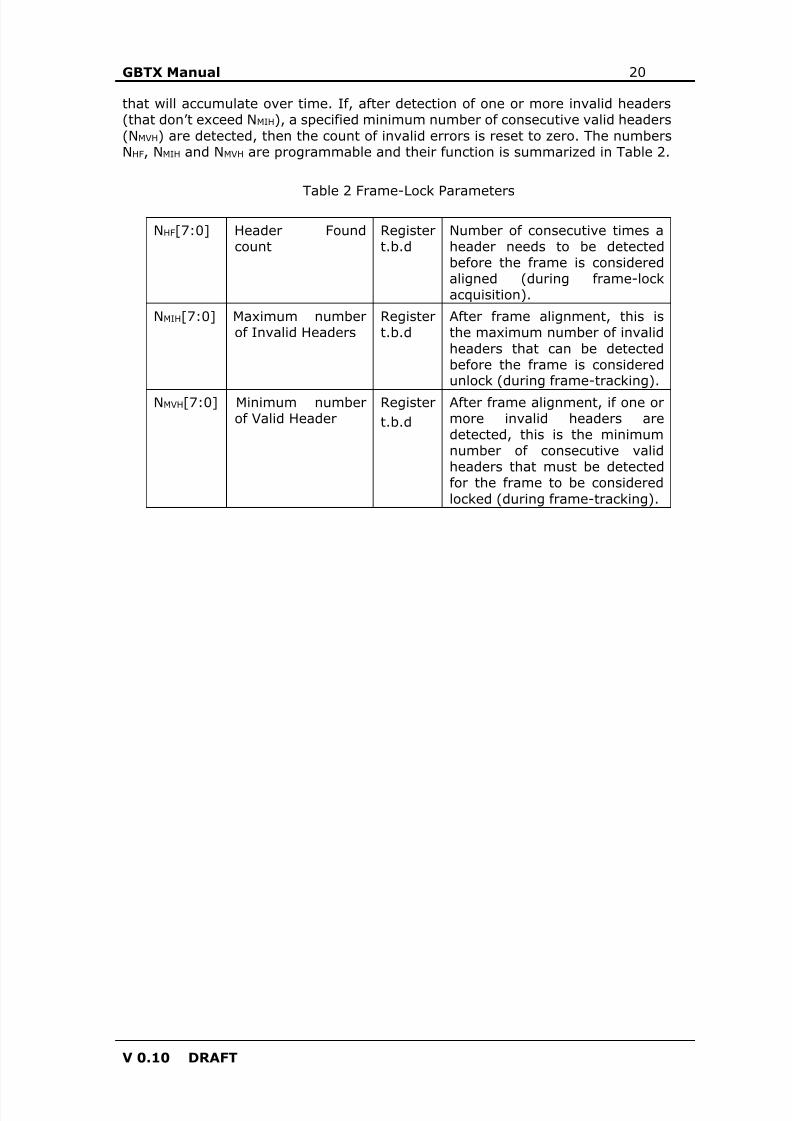
that will accumulate over time. If, after detection of one or more invalid headers(that don’t exceed N MIH), a specified minimum number of consecutive valid headers(N MVH) are detected, then the count of invalid errors is reset to zero. The numbersNHF, N MIH and N MVH are programmable and their function is summarized in Table 2.
Table 2 Frame-Lock Parameters
NHF[7:0] Header Foundcount
Registert.b.d
Number of consecutive times aheader needs to be detectedbefore the frame is consideredaligned (during frame-lockacquisition).
NMIH[7:0] Maximum numberof Invalid Headers
Registert.b.d
After frame alignment, this isthe maximum number of invalidheaders that can be detectedbefore the frame is consideredunlock (during frame-tracking).
NMVH[7:0] Minimum numberof Valid Header
Registert.b.d
After frame alignment, if one ormore invalid headers aredetected, this is the minimumnumber of consecutive validheaders that must be detectedfor the frame to be consideredlocked (during frame-tracking).
8/15/2019 gbtx Manual
http://slidepdf.com/reader/full/gbtx-manual 21/200
GBTX Manual 21
V 0.10 DRAFT
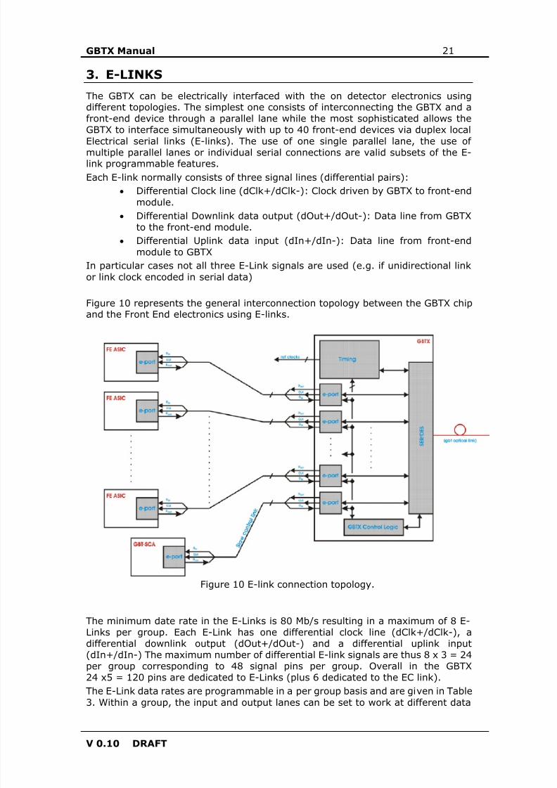
3. E-LINKS
The GBTX can be electrically interfaced with the on detector electronics usingdifferent topologies. The simplest one consists of interconnecting the GBTX and afront-end device through a parallel lane while the most sophisticated allows theGBTX to interface simultaneously with up to 40 front-end devices via duplex localElectrical serial links (E-links). The use of one single parallel lane, the use ofmultiple parallel lanes or individual serial connections are valid subsets of the E-link programmable features.Each E-link normally consists of three signal lines (differential pairs):
• Differential Clock line (dClk+/dClk-): Clock driven by GBTX to front-endmodule.
• Differential Downlink data output (dOut+/dOut-): Data line from GBTXto the front-end module.
• Differential Uplink data input (dIn+/dIn-): Data line from front-endmodule to GBTX
In particular cases not all three E-Link signals are used (e.g. if unidirectional linkor link clock encoded in serial data)
Figure 10 represents the general interconnection topology between the GBTX chipand the Front End electronics using E-links.
Figure 10 E-link connection topology.
The minimum date rate in the E-Links is 80 Mb/s resulting in a maximum of 8 E-Links per group. Each E-Link has one differential clock line (dClk+/dClk-), adifferential downlink output (dOut+/dOut-) and a differential uplink input(dIn+/dIn-) The maximum number of differential E-link signals are thus 8 x 3 = 24per group corresponding to 48 signal pins per group. Overall in the GBTX24 x5 = 120 pins are dedicated to E-Links (plus 6 dedicated to the EC link).
The E-Link data rates are programmable in a per group basis and are given in Table3. Within a group, the input and output lanes can be set to work at different data
8/15/2019 gbtx Manual
http://slidepdf.com/reader/full/gbtx-manual 22/200
GBTX Manual 22
V 0.10 DRAFT
rates and an unused group can be turned off to reduce the power consumption inthe corresponding internal logic.The bit shift in/out order for the E-Link data inputs and outputs is MSB first.
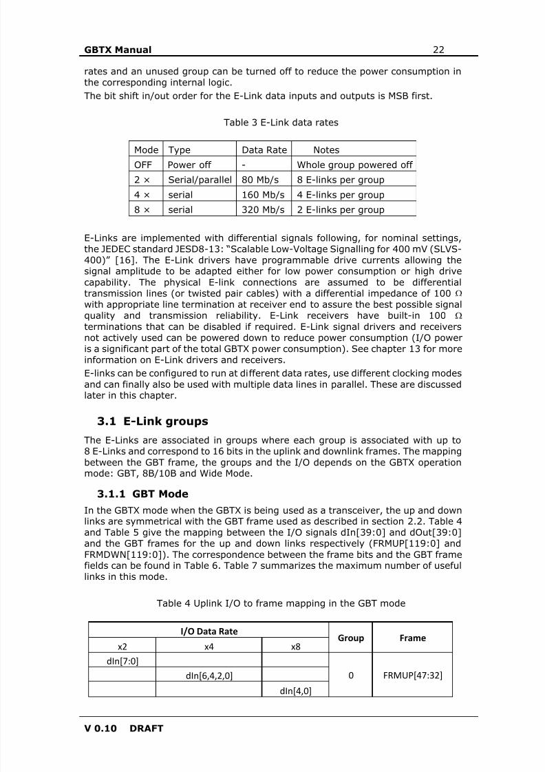
Table 3 E-Link data rates
Mode Type Data Rate NotesOFF Power off - Whole group powered off2 × Serial/parallel 80 Mb/s 8 E-links per group4 × serial 160 Mb/s 4 E-links per group8 × serial 320 Mb/s 2 E-links per group
E-Links are implemented with differential signals following, for nominal settings,the JEDEC standard JESD8-13: “Scalable Low-Voltage Signalling for 400 mV (SLVS-400)” [16] . The E-Link drivers have programmable drive currents allowing thesignal amplitude to be adapted either for low power consumption or high drivecapability. The physical E-link connections are assumed to be differentialtransmission lines (or twisted pair cables) with a differential impedance of 100 Ω with appropriate line termination at receiver end to assure the best possible signalquality and transmission reliability. E-Link receivers have built-in 100 Ω terminations that can be disabled if required. E-Link signal drivers and receiversnot actively used can be powered down to reduce power consumption (I/O poweris a significant part of the total GBTX power consumption). See chapter 13 for moreinformation on E-Link drivers and receivers.E-links can be configured to run at different data rates, use different clocking modesand can finally also be used with multiple data lines in parallel. These are discussedlater in this chapter.
3.1 E-Link groups
The E-Links are associated in groups where each group is associated with up to8 E-Links and correspond to 16 bits in the uplink and downlink frames. The mappingbetween the GBT frame, the groups and the I/O depends on the GBTX operationmode: GBT, 8B/10B and Wide Mode.
3.1.1 GBT Mode
In the GBTX mode when the GBTX is being used as a transceiver, the up and downlinks are symmetrical with the GBT frame used as described in section 2.2. Table 4and Table 5 give the mapping between the I/O signals dIn[39:0] and dOut[39:0]and the GBT frames for the up and down links respectively (FRMUP[119:0] andFRMDWN[119:0]). The correspondence between the frame bits and the GBT framefields can be found in Table 6. Table 7 summarizes the maximum number of usefullinks in this mode.
Table 4 Uplink I/O to frame mapping in the GBT mode
I/O Data RateGroup Frame
x2 x4 x8
dIn[7:0]
0 FRMUP[47:32]dIn[6,4,2,0]dIn[4,0]
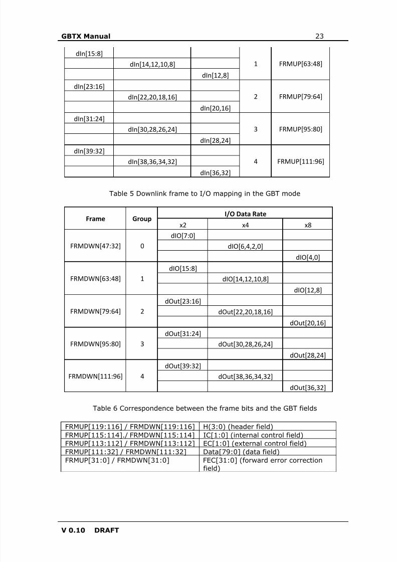
8/15/2019 gbtx Manual
http://slidepdf.com/reader/full/gbtx-manual 23/200
GBTX Manual 23
V 0.10 DRAFT
dIn[15:8]1 FRMUP[63:48]dIn[14,12,10,8]
dIn[12,8]
dIn[23:16]
2 FRMUP[79:64]dIn[22,20,18,16]dIn[20,16]
dIn[31:24]3 FRMUP[95:80]dIn[30,28,26,24]
dIn[28,24]
dIn[39:32]4 FRMUP[111:96]dIn[38,36,34,32]
dIn[36,32]
Table 5 Downlink frame to I/O mapping in the GBT mode
Frame GroupI/O Data Rate
x2 x4 x8
FRMDWN[47:32] 0dIO[7:0]
dIO[6,4,2,0]
dIO[4,0]
FRMDWN[63:48] 1dIO[15:8]
dIO[14,12,10,8]
dIO[12,8]
FRMDWN[79:64] 2dOut[23:16]
dOut[22,20,18,16]
dOut[20,16]
FRMDWN[95:80] 3dOut[31:24]
dOut[30,28,26,24]
dOut[28,24]
FRMDWN[111:96] 4dOut[39:32]
dOut[38,36,34,32]
dOut[36,32]
Table 6 Correspondence between the frame bits and the GBT fields
FRMUP[119:116] / FRMDWN[119:116] H(3:0) (header field)FRMUP[115:114]./ FRMDWN[115:114] IC[1:0] (internal control field)FRMUP[113:112] / FRMDWN[113:112] EC[1:0] (external control field)FRMUP[111:32] / FRMDWN[111:32] Data[79:0] (data field)FRMUP[31:0] / FRMDWN[31:0] FEC[31:0] (forward error correction
field)
8/15/2019 gbtx Manual
http://slidepdf.com/reader/full/gbtx-manual 24/200
GBTX Manual 24
V 0.10 DRAFT
Table 7 Maximum number of Up/Down links in the GBT mode
E-Link Data Rate 80 Mb/s 160 Mb/s 320 Mb/sMax # of up-links 40 20 10
Max # of down-links 40 20 10
3.1.2 Wide Bus Mode
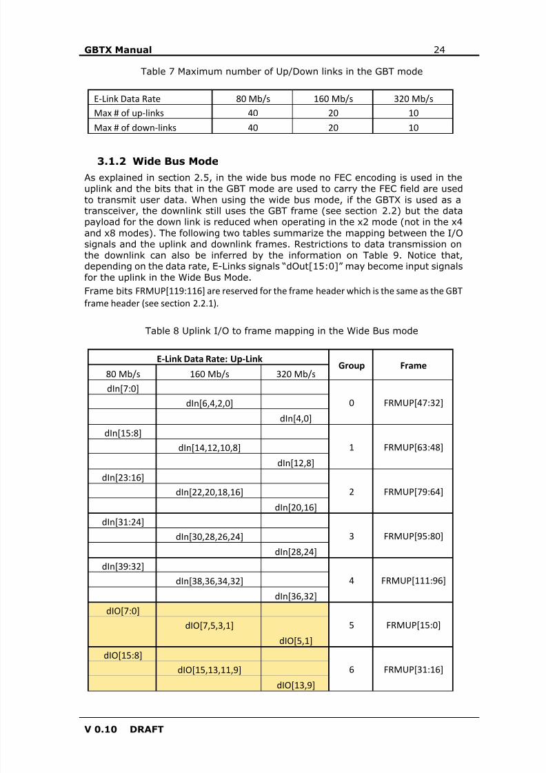
As explained in section 2.5, in the wide bus mode no FEC encoding is used in theuplink and the bits that in the GBT mode are used to carry the FEC field are usedto transmit user data. When using the wide bus mode, if the GBTX is used as atransceiver, the downlink still uses the GBT frame (see section 2.2) but the datapayload for the down link is reduced when operating in the x2 mode (not in the x4and x8 modes). The following two tables summarize the mapping between the I/Osignals and the uplink and downlink frames. Restrictions to data transmission onthe downlink can also be inferred by the information on Table 9. Notice that,
depending on the data rate, E-Links signals “dOut[15:0]” may become input signalsfor the uplink in the Wide Bus Mode.Frame bits FRMUP[119:116] are reserved for the frame header which is the same as the GBTframe header (see section 2.2.1) .
Table 8 Uplink I/O to frame mapping in the Wide Bus mode
E-Link Data Rate: Up-LinkGroup Frame
80 Mb/s 160 Mb/s 320 Mb/s
dIn[7:0]
0 FRMUP[47:32]dIn[6,4,2,0]dIn[4,0]
dIn[15:8]1 FRMUP[63:48]dIn[14,12,10,8]
dIn[12,8]
dIn[23:16]2 FRMUP[79:64]dIn[22,20,18,16]
dIn[20,16]
dIn[31:24]3 FRMUP[95:80]dIn[30,28,26,24]
dIn[28,24]
dIn[39:32]4 FRMUP[111:96]dIn[38,36,34,32]
dIn[36,32]
dIO[7:0]5 FRMUP[15:0]dIO[7,5,3,1]
dIO[5,1]
dIO[15:8]6 FRMUP[31:16]dIO[15,13,11,9]
dIO[13,9]
8/15/2019 gbtx Manual
http://slidepdf.com/reader/full/gbtx-manual 25/200
GBTX Manual 25
V 0.10 DRAFT
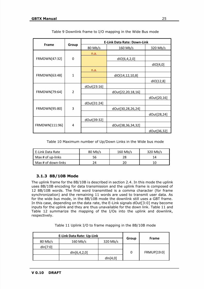
Table 9 Downlink frame to I/O mapping in the Wide Bus mode
Frame GroupE-Link Data Rate: Down-Link
80 Mb/s 160 Mb/s 320 Mb/s
FRMDWN[47:32] 0n.a.
dIO[6,4,2,0]
dIO[4,0]
FRMDWN[63:48] 1n.a.
dIO[14,12,10,8]
dIO[12,8]
FRMDWN[79:64] 2dOut[23:16]
dOut[22,20,18,16]
dOut[20,16]
FRMDWN[95:80] 3dOut[31:24]
dOut[30,28,26,24]
dOut[28,24]
FRMDWN[111:96] 4dOut[39:32]
dOut[38,36,34,32]
dOut[36,32]
Table 10 Maximum number of Up/Down Links in the Wide bus mode
E-Link Data Rate 80 Mb/s 160 Mb/s 320 Mb/sMax # of up-links 56 28 14
Max # of down-links 24 20 10
3.1.3 8B/10B Mode
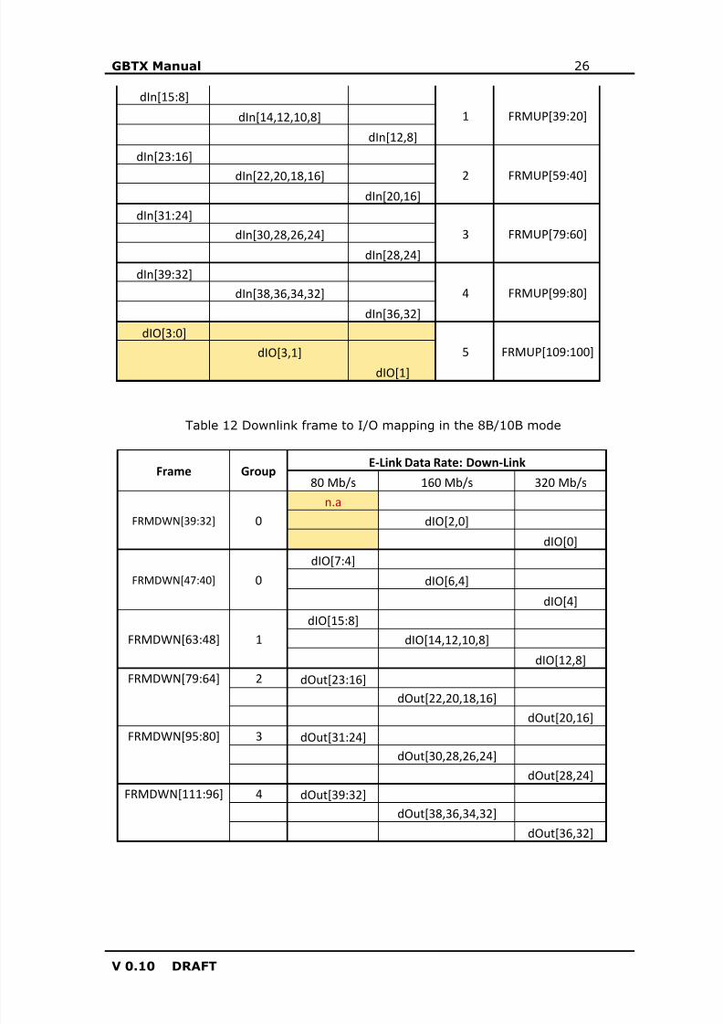
The uplink frame for the 8B/10B is described in section 2.4. In this mode the uplinkuses 8B/10B encoding for data transmission and the uplink frame is composed of12 8B/10B words. The first word transmitted is a comma character (for framesynchronization) and the remaining 11 words are used to transmit user data. Asfor the wide bus mode, in the 8B/10B mode the downlink still uses a GBT frame.In this case, depending on the data rate, the E-Link signals dOut[3:0] may becomeinputs for the uplink and they are thus unavailable for the down link. Table 11 andTable 12 summarize the mapping of the I/Os into the uplink and downlink,respectively.
Table 11 Uplink I/O to frame mapping in the 8B/10B mode
E-Link Data Rate: Up-LinkGroup Frame
80 Mb/s 160 Mb/s 320 Mb/s
dIn[7:0]
0 FRMUP[19:0]dIn[6,4,2,0]dIn[4,0]
8/15/2019 gbtx Manual
http://slidepdf.com/reader/full/gbtx-manual 26/200
GBTX Manual 26
V 0.10 DRAFT
dIn[15:8]
1 FRMUP[39:20]dIn[14,12,10,8]
dIn[12,8]
dIn[23:16]
2 FRMUP[59:40]dIn[22,20,18,16]dIn[20,16]
dIn[31:24]3 FRMUP[79:60]dIn[30,28,26,24]
dIn[28,24]
dIn[39:32]4 FRMUP[99:80]dIn[38,36,34,32]
dIn[36,32]
dIO[3:0]5 FRMUP[109:100]
dIO[3,1]dIO[1]
Table 12 Downlink frame to I/O mapping in the 8B/10B mode
Frame GroupE-Link Data Rate: Down-Link
80 Mb/s 160 Mb/s 320 Mb/s
FRMDWN[39:32] 0n.a
dIO[2,0]
dIO[0]
FRMDWN[47:40] 0
dIO[7:4]
dIO[6,4]
dIO[4]
FRMDWN[63:48] 1dIO[15:8]
dIO[14,12,10,8]
dIO[12,8]FRMDWN[79:64] 2 dOut[23:16]
dOut[22,20,18,16]
dOut[20,16]FRMDWN[95:80] 3 dOut[31:24]
dOut[30,28,26,24]
dOut[28,24]FRMDWN[111:96] 4 dOut[39:32]
dOut[38,36,34,32]
dOut[36,32]
8/15/2019 gbtx Manual
http://slidepdf.com/reader/full/gbtx-manual 27/200
GBTX Manual 27
V 0.10 DRAFT
Table 13 Maximum number of Up/Down Links in the 8B/10B mode
E-Link Data Rate 80 Mb/s 160 Mb/s 320 Mb/sMax # of up-links 44 22 11
Max # of down-links 36 20 10
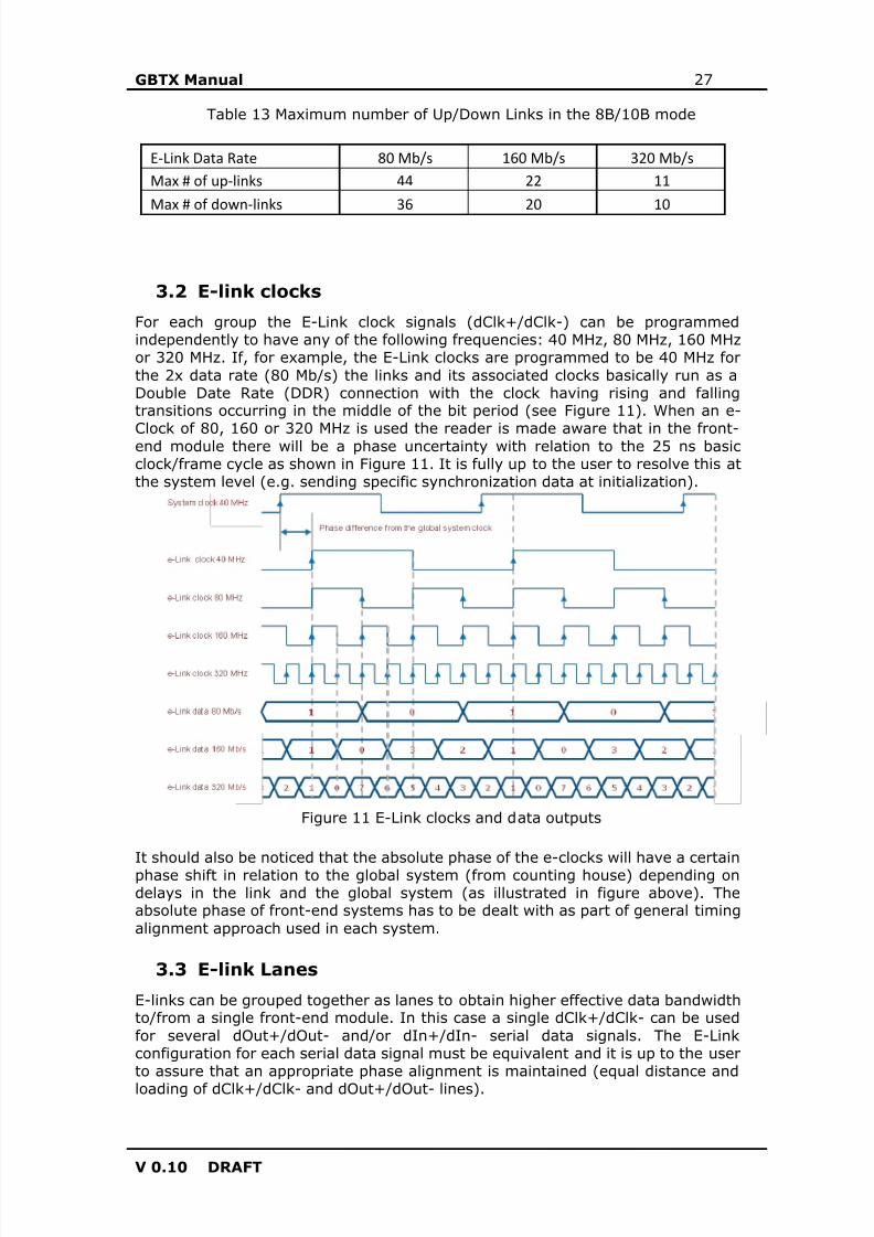
3.2 E-link clocks
For each group the E-Link clock signals (dClk+/dClk-) can be programmedindependently to have any of the following frequencies: 40 MHz, 80 MHz, 160 MHzor 320 MHz. If, for example, the E-Link clocks are programmed to be 40 MHz forthe 2x data rate (80 Mb/s) the links and its associated clocks basically run as aDouble Date Rate (DDR) connection with the clock having rising and fallingtransitions occurring in the middle of the bit period (see Figure 11) . When an e-
Clock of 80, 160 or 320 MHz is used the reader is made aware that in the front-end module there will be a phase uncertainty with relation to the 25 ns basicclock/frame cycle as shown in Figure 11. It is fully up to the user to resolve this atthe system level (e.g. sending specific synchronization data at initialization).
Figure 11 E-Link clocks and data outputs
It should also be noticed that the absolute phase of the e-clocks will have a certainphase shift in relation to the global system (from counting house) depending ondelays in the link and the global system (as illustrated in figure above). Theabsolute phase of front-end systems has to be dealt with as part of general timingalignment approach used in each system.
3.3 E-link Lanes
E-links can be grouped together as lanes to obtain higher effective data bandwidthto/from a single front-end module. In this case a single dClk+/dClk- can be usedfor several dOut+/dOut- and/or dIn+/dIn- serial data signals. The E-Linkconfiguration for each serial data signal must be equivalent and it is up to the userto assure that an appropriate phase alignment is maintained (equal distance andloading of dClk+/dClk- and dOut+/dOut- lines).
8/15/2019 gbtx Manual
http://slidepdf.com/reader/full/gbtx-manual 28/200
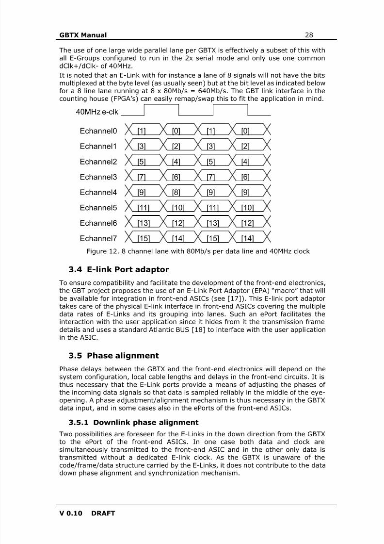
GBTX Manual 28
V 0.10 DRAFT
The use of one large wide parallel lane per GBTX is effectively a subset of this withall E-Groups configured to run in the 2x serial mode and only use one commondClk+/dClk- of 40MHz.It is noted that an E-Link with for instance a lane of 8 signals will not have the bitsmultiplexed at the byte level (as usually seen) but at the bit level as indicated belowfor a 8 line lane running at 8 x 80Mb/s = 640Mb/s. The GBT link interface in thecounting house (FPGA’s) can easily remap/swap this to fit the application in mind.
Figure 12. 8 channel lane with 80Mb/s per data line and 40MHz clock
3.4 E-link Port adaptor
To ensure compatibility and facilitate the development of the front-end electronics,the GBT project proposes the use of an E-Link Port Adaptor (EPA) “macro” that willbe available for integration in front-end ASICs (see [17] ). This E-link port adaptortakes care of the physical E-link interface in front-end ASICs covering the multipledata rates of E-Links and its grouping into lanes. Such an ePort facilitates theinteraction with the user application since it hides from it the transmission framedetails and uses a standard Atlantic BUS [18] to interface with the user applicationin the ASIC.
3.5 Phase alignment
Phase delays between the GBTX and the front-end electronics will depend on thesystem configuration, local cable lengths and delays in the front-end circuits. It isthus necessary that the E-Link ports provide a means of adjusting the phases ofthe incoming data signals so that data is sampled reliably in the middle of the eye-opening. A phase adjustment/alignment mechanism is thus necessary in the GBTXdata input, and in some cases also in the ePorts of the front-end ASICs.
3.5.1 Downlink phase alignment
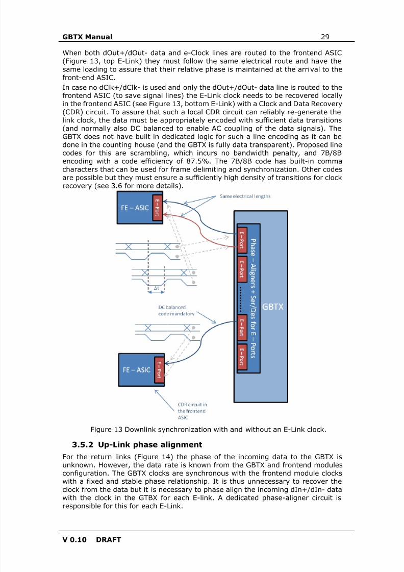
Two possibilities are foreseen for the E-Links in the down direction from the GBTXto the ePort of the front-end ASICs. In one case both data and clock aresimultaneously transmitted to the front-end ASIC and in the other only data istransmitted without a dedicated E-link clock. As the GBTX is unaware of thecode/frame/data structure carried by the E-Links, it does not contribute to the datadown phase alignment and synchronization mechanism.
[1] [0] [1] [0]
[3] [2] [3] [2]
[5] [4] [5] [4]
[7] [6] [7] [6]
[9] [8] [9] [9]
[11] [10] [11] [10]
[13] [12] [13] [12]
[15] [14] [15] [14]
Echannel0
40MHz e-clk
Echannel1
Echannel2
Echannel3
Echannel4
Echannel5
Echannel6
Echannel7
8/15/2019 gbtx Manual
http://slidepdf.com/reader/full/gbtx-manual 29/200
GBTX Manual 29
V 0.10 DRAFT
When both dOut+/dOut- data and e-Clock lines are routed to the frontend ASIC(Figure 13, top E-Link) they must follow the same electrical route and have thesame loading to assure that their relative phase is maintained at the arrival to thefront-end ASIC.In case no dClk+/dClk- is used and only the dOut+/dOut- data line is routed to thefrontend ASIC (to save signal lines) the E-Link clock needs to be recovered locallyin the frontend ASIC (see Figure 13, bottom E-Link) with a Clock and Data Recovery(CDR) circuit. To assure that such a local CDR circuit can reliably re-generate thelink clock, the data must be appropriately encoded with sufficient data transitions(and normally also DC balanced to enable AC coupling of the data signals). TheGBTX does not have built in dedicated logic for such a line encoding as it can bedone in the counting house (and the GBTX is fully data transparent). Proposed linecodes for this are scrambling, which incurs no bandwidth penalty, and 7B/8Bencoding with a code efficiency of 87.5%. The 7B/8B code has built-in commacharacters that can be used for frame delimiting and synchronization. Other codesare possible but they must ensure a sufficiently high density of transitions for clockrecovery (see 3.6 for more details).
Figure 13 Downlink synchronization with and without an E-Link clock.
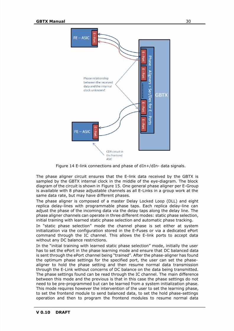
3.5.2 Up-Link phase alignment
For the return links (Figure 14) the phase of the incoming data to the GBTX isunknown. However, the data rate is known from the GBTX and frontend modulesconfiguration. The GBTX clocks are synchronous with the frontend module clockswith a fixed and stable phase relationship. It is thus unnecessary to recover theclock from the data but it is necessary to phase align the incoming dIn+/dIn- data
with the clock in the GTBX for each E-link. A dedicated phase-aligner circuit isresponsible for this for each E-Link.
8/15/2019 gbtx Manual
http://slidepdf.com/reader/full/gbtx-manual 30/200
GBTX Manual 30
V 0.10 DRAFT
Figure 14 E-link connections and phase of dIn+/dIn- data signals.
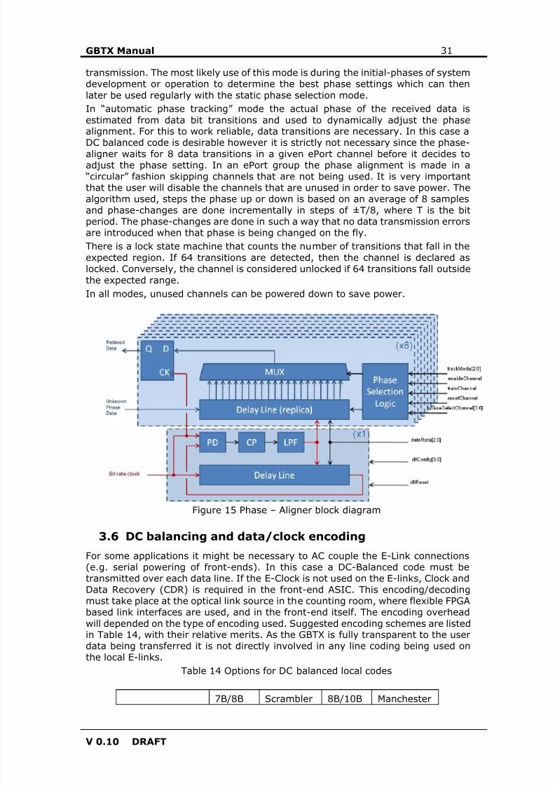
The phase aligner circuit ensures that the E-link data received by the GBTX issampled by the GBTX internal clock in the middle of the eye-diagram. The blockdiagram of the circuit is shown in Figure 15. One general phase aligner per E-Groupis available with 8 phase adjustable channels as all E-Links in a group work at thesame data rate, but may have different phases.The phase aligner is composed of a master Delay Locked Loop (DLL) and eightreplica delay-lines with programmable phase taps. Each replica delay-line canadjust the phase of the incoming data via the delay taps along the delay line. Thephase aligner channels can operate in three different modes: static phase selection,initial training with learned static phase selection and automatic phase tracking.In “static phase selection” mode the channel phase is set either at system
initialization via the configuration stored in the E-Fuses or via a dedicated ePortcommand through the IC channel. This allows the E-link ports to accept datawithout any DC balance restrictions.In the “initial training with learned static phase selection” mode, initially the userhas to set the ePort in the phase learning mode and ensure that DC balanced datais sent through the ePort channel being “trained”. After the phase-aligner has foundthe optimum phase settings for the specified port, the user can set the phase-aligner to hold the phase setting and then resume normal data transmissionthrough the E-Link without concerns of DC balance on the data being transmitted.The phase settings found can be read through the IC channel. The main differencebetween this mode and the previous is that in this case the phase settings do notneed to be pre-programmed but can be learned from a system initialization phase.
This mode requires however the intervention of the user to set the learning phase,to set the frontend module to send balanced data, to set the hold phase-settingsoperation and then to program the frontend modules to resume normal data
8/15/2019 gbtx Manual
http://slidepdf.com/reader/full/gbtx-manual 31/200
GBTX Manual 31
V 0.10 DRAFT
transmission. The most likely use of this mode is during the initial-phases of systemdevelopment or operation to determine the best phase settings which can thenlater be used regularly with the static phase selection mode.In “automatic phase tracking” mode the actual phase of the received data isestimated from data bit transitions and used to dynamically adjust the phasealignment. For this to work reliable, data transitions are necessary. In this case aDC balanced code is desirable however it is strictly not necessary since the phase-aligner waits for 8 data transitions in a given ePort channel before it decides toadjust the phase setting. In an ePort group the phase alignment is made in a
“circular” fashion skipping channels that are not being used. It is very importantthat the user will disable the channels that are unused in order to save power. Thealgorithm used, steps the phase up or down is based on an average of 8 samplesand phase-changes are done incrementally in steps of ±T/8, where T is the bitperiod. The phase-changes are done in such a way that no data transmission errorsare introduced when that phase is being changed on the fly.There is a lock state machine that counts the number of transitions that fall in theexpected region. If 64 transitions are detected, then the channel is declared aslocked. Conversely, the channel is considered unlocked if 64 transitions fall outsidethe expected range.In all modes, unused channels can be powered down to save power.
Figure 15 Phase – Aligner block diagram
3.6 DC balancing and data/clock encoding
For some applications it might be necessary to AC couple the E-Link connections(e.g. serial powering of front-ends). In this case a DC-Balanced code must betransmitted over each data line. If the E-Clock is not used on the E-links, Clock andData Recovery (CDR) is required in the front-end ASIC. This encoding/decodingmust take place at the optical link source in the counting room, where flexible FPGAbased link interfaces are used, and in the front-end itself. The encoding overheadwill depended on the type of encoding used. Suggested encoding schemes are listedin Table 14, with their relative merits. As the GBTX is fully transparent to the userdata being transferred it is not directly involved in any line coding being used onthe local E-links.
Table 14 Options for DC balanced local codes
7B/8B Scrambler 8B/10B Manchester
8/15/2019 gbtx Manual
http://slidepdf.com/reader/full/gbtx-manual 32/200
GBTX Manual 32
V 0.10 DRAFT
“Odd” word size Yes No Yes NoUser bandwidth 87.5% 100% 80% 50%Frame synch.
“built in”Yes No Yes No
3.7 Programming the E-Links
Programing the E-Links involves the following operations:Clock ports:
• Set the clock bus frequency for each group;• Enable individual clock ports on each group;• Set the clock drivers strength per group.
Data output ports:• Set the data rate for each group;
o For 160 and 320 Mb/s the E-PLL RX needs to be enabled and
configured (see section 9.5) .• Enable individual data ports on each group.• Set the data drivers strength per group;
Data input ports:• Set the phase-aligner mode (common to all the groups);• Set the DLL parameters for each group.• Set the data rate for each group;
o For 160 and 320 Mb/s the E-PLL TX needs to be enabled andconfigured (see section 9.5) .
• Enable individual data ports on each group.• Depending on the mode: select the phase for each active channel or
execute a train/hold sequence for each active channel or set theautomatic phase align mode.
Note that the input and output data rates can be programmed independentlyfrom each other and the clock frequencies independently form theinput/output data rates.
3.7.1 Programming the E-Link clocks
All the clocks in a group have the same frequency; however the groupfrequency can be set independently of the data rate programed for the datainputs and outputs of that group.
The registers that program the clock bus frequency and enable/disable theclock ports are triplicated and consequently each Triple Modular Redundancy(TMR) register must contain the same data; the user must ensure that thisis the case.Table 15 to Table 17 innumerate the registers used to set the clock busfrequencies and the corresponding clock settings.
Table 15 E-Link clock frequency programing registers
Register Register Name Function (see Table 16)
254 [3:2] outEportCtr0[3:2] clockBusFrequencyA0[3:2]257 [3:2] outEportCtr3[3:2] clockBusFrequencyA1[3:2]
8/15/2019 gbtx Manual
http://slidepdf.com/reader/full/gbtx-manual 33/200
GBTX Manual 33
V 0.10 DRAFT
260 [3:2] outEportCtr6[3:2] clockBusFrequencyA2[3:2]263 [3:2] outEportCtr9[3:2] clockBusFrequencyA3[3:2]266 [3:2] outEportCtr12[3:2] clockBusFrequencyA4[3:2]332 [3:2] outEportCtr20[3:2] clockBusFrequencyB0[3:2]
335 [3:2] outEportCtr23[3:2] clockBusFrequencyB1[3:2]338 [3:2] outEportCtr26[3:2] clockBusFrequencyB2[3:2]341 [3:2] outEportCtr29[3:2] clockBusFrequencyB3[3:2]344 [3:2] outEportCtr32[3:2] clockBusFrequencyB4[3:2]347 [3:2] outEportCtr35[3:2] clockBusFrequencyC0[3:2]350 [3:2] outEportCtr38[3:2] clockBusFrequencyC1[3:2]353 [3:2] outEportCtr41[3:2] clockBusFrequencyC2[3:2]356 [3:2] outEportCtr44[3:2] clockBusFrequencyC3[3:2]359 [3:2] outEportCtr47[3:2] clockBusFrequencyC4[3:2]
Table 16 E-Link clock frequency settings
clockBusFrequencyYX[3:2]with Y = A, B and C
X = 0, 1, 2, 3 and 4
Clock frequency in MHz
2’b00 402’b01 802’b10 160
2’b11 320
Table 17 EC port clock settings
Register 257[6:4] = outEportCtr3[3:2] =clockBusFrequencyEcC, clockBusFrequencyEcB,clockBusFrequencyEcA
Clockfrequency inMHz
3’b000 403’b111 80Other combinations not allowed
Individual clock lines are enabled/disabled according to the data in Table18. A zero in the corresponding channel bit will disable the channel while aone will enable it. Unused channels should be disabled to save power. Thebit correspondence is bit 0 to channel 0, bit 1 to channel 1, etc.
Table 18 Clock port enable registers
Register Register Name Function
255 [7:0] outEportCtr1[7:0] clockPortEnableGroupA0[7:0]258 [7:0] outEportCtr4[7:0] clockPortEnableGroupA1[7:0]
8/15/2019 gbtx Manual
http://slidepdf.com/reader/full/gbtx-manual 34/200
GBTX Manual 34
V 0.10 DRAFT
261 [7:0] outEportCtr7[7:0] clockPortEnableGroupA2[7:0]264 [7:0] outEportCtr10[7:0] clockPortEnableGroupA3[7:0]267 [7:0] outEportCtr13[7:0] clockPortEnableGroupA4[7:0]333 [7:0] outEportCtr21[7:0] clockPortEnableGroupB0[7:0]
336 [7:0] outEportCtr24[7:0] clockPortEnableGroupB1[7:0]339 [7:0] outEportCtr27[7:0] clockPortEnableGroupB2[7:0]342 [7:0] outEportCtr30[7:0] clockPortEnableGroupB3[7:0]345 [7:0] outEportCtr33[7:0] clockPortEnableGroupB4[7:0]348 [7:0] outEportCtr36[7:0] clockPortEnableGroupC0[7:0]351 [7:0] outEportCtr39[7:0] clockPortEnableGroupC1[7:0]354 [7:0] outEportCtr42[7:0] clockPortEnableGroupC2[7:0]357 [7:0] outEportCtr45[7:0] clockPortEnableGroupC3[7:0]360 [7:0] outEportCtr48[7:0] clockPortEnableGroupC4[7:0]
8/15/2019 gbtx Manual
http://slidepdf.com/reader/full/gbtx-manual 35/200
GBTX Manual 35
V 0.10 DRAFT
4. LATENCY AND PHASE STABILITY
The GTBX guarantees constant latency over time and from one power-up/initialization to the next. Constant latency enables the GBTX to be used in clocksynchronous trigger systems and for precise TTC distribution to the many front-end destinations. It is brought to the attention of the reader that this is for theGBTX itself but does not necessarily apply to the link interface made in FPGA’s forthe off detector part of the link (see separate GBT documentation for this part inchapter 20) .There will inevitable be some phase variation of a complete link because oftemperature/voltage variations in different parts of the link system. At presenttime, the sensitivity of the GBTX phase with temperature and voltage is still beingevaluated.More information on this topic will be added in this chapter...
Latency from simulations:The ePorts depend on exactly how the phases of the clocks are.
But I think we can get the worst cases (in units of 25ns):TX = 5 (if 8b10b is used)RX = 4.5
8/15/2019 gbtx Manual
http://slidepdf.com/reader/full/gbtx-manual 36/200
GBTX Manual 36
V 0.10 DRAFT
5. GBTX REGISTER ACCESS
As discussed in section 2.2.2 four bits of the GBT frame are reserved for slowcontrol applications. Two of these bits (IC[1:0]) are reserved for control andmonitoring of the GBTX operation. The other two (EC[1:0]) are made availableexternally to allow the implementation of a slow control link to another chip,however their actual use is not restricted to that type of applications. The GBTXcan also be controlled and monitored via an I2C interface as an alternative tothe IC channel. The selection of IC or I2C is made using the pin configSelect.More details are given below and in Section 17. When I2C mode is selected, the user should ensure that the bits IC[1:0] in thedownlink GBTX frame are set to 2’b11.
5.1 IC control and monitoring channel
Data field bits IC[1:0] are reserved for control and monitoring of the GBTXoperation. These 2 bits implement an 80 Mb/s serial channel that is used toread and write the GBTX internal registers. This channel is used at start-up toconfigure the GBTX and during normal operation to program and monitor theoperation of the GBTX.Programming of the GBTX through this channel can be done when the GBTX isoperated in Transceiver mode. The registers in the GBLD can also be accessedby this route via a simplified I2C port between the GBTX and the GBLD (seechapter 6) . The two bits IC[1:0] of the SC field in the received GBT framecontain the configuration data. These are de-multiplexed to form 8-bit wordswhich follow a frame-based protocol. The protocol for data sent to the GBTX fora write-read operation is shown in Table 19 and for a read-only operation inTable 20. When a write-read or read-only frame is received by the GBTX and theaddresses matches the ASIC I2C address (see section 5.2.1) , the GBTX willacknowledge receipt of the data by sending a similar frame back on the uplink.GBTXs that are not addressed will not return any data. A broadcast address(7’b0000000) can be used to write the same data to a number of GBTXs. Inthis case, the GBTX will not send the acknowledge frame back on the uplink.Note that the GBTX will not carry out any subsequent operations until the readsequence is complete. Also note that this operation is not possible if the GBTXis in simplex receiver mode.
Table 19 IC channel frame structure sent to GBTX for a write-read sequence
A Frame delimiter 8’b 01111110 Not in parity check
B GBTX i2c address (7 bits) + R/W bit = 0 Not in parity checkC Command (8 bits) In parity checkD Number of data words n[7:0] In parity check
Number of data words n[15:8] In parity checkE Memory address [7:0] In parity check
Memory address [15:8] In parity checkF 1st data (8 bits) In parity check
………… In parity checknth data (8 bits) In parity check
G Parity word (8 bits) In parity checkA Frame delimiter 8’b 01111110 Not in parity check
8/15/2019 gbtx Manual
http://slidepdf.com/reader/full/gbtx-manual 37/200
GBTX Manual 37
V 0.10 DRAFT
Table 20 IC channel frame structure sent to GBTX in a read-only sequence
A Frame delimiter 8’b 01111110 Not in parity checkB GBTX i2c address (7 bits) + R/W bit = 1 Not in parity checkC Command (8 bits) In parity check
D Number of data words n[7:0] In parity checkNumber of data words n[15:8] In parity checkE Memory address [7:0] In parity check
Memory address [15:8] In parity checkG Parity word (8 bits) In parity checkA Frame delimiter 8’b 01111110 Not in parity check
As shown in tables Table 19 and Table 20 the write-read and write-onlyoperations follow the following structure:
A) The beginning and end of the frame are marked with the delimiter word (8’b01111110). To ensure that a payload word is not misinterpreted as thedelimiter, bit stuffing is used so that any sequence of five consecutive 1s inthe payload is always followed by a 0. This bit-stuffing must be carried outby the corresponding transmitter and the de-stuffing by the receiver.
B) An address word is then transmitted and contains the 7-bit address of thatparticular GBTX and a Read/Write (R/W) bit. Notice that the IC channeladdress is the same as the I2C (see section 5.2.1) . If the address does notmatch, then the subsequent actions are not carried out and the GBTX willnot send the acknowledge frame back on the uplink. If the R/W bit is 1, thenthe configuration registers are not modified but their contents are read backin the transmitted GBT frame. If the R/W bit is 0, then the registers areover-written with the values transmitted within this frame. The new valuesare read back in the transmitted GBT frame.
C) A Command word is then transmitted. In version 1 and 2 of the GBTX, thedata in this word is ignored.
D) This is followed by two bytes to indicate the number of data words (n) inthe packet, maximum 65k.
E) Then the internal address (2 bytes) of the first register to be accessed istransmitted.
F) The n data words then follow. This scheme allows access to a single registeror a block of registers in consecutive memory addresses. In the frame for aread-only sequence, no data bytes are transmitted to the GBTX.
G) Finally, a parity word is transmitted where each bit is the final parity of thatbit through all bytes of the frame, except the frame delimiters and the firstbyte “GBTX i2c address + R/W”. The user should calculate a running parityand transmit it as this final word. The GBTX constructs the same parity sumfrom the received data and compares it to the last word of the data packet.The result of this comparison is stored in a status register and can beaccessed by the user (logic 1 if the parity check was OK).
Return FrameThe structure of the frame returned by the GBTX is the same as in Table 19, with the exception of the Command word. Here, the word consists of seven 0sconcatenated with an LSB which is the status bit of the previous parity check(logic 1 if the parity check was OK). Independently of the result of the paritycheck, if this is a write-read operation, the data payload is always written tothe respective registers and the data bytes in the returned frame are the new

8/15/2019 gbtx Manual
http://slidepdf.com/reader/full/gbtx-manual 38/200
GBTX Manual 38
V 0.10 DRAFT
values that have just been written into the registers. The parity word returnedis calculated based on these values.The last parity bit check result can be read from bit zero of registers 371, 372and 373, that is:
Register 371[0] = scStatusA[0] = parity bit ARegister 372[0] = scStatusB[0] = parity bit BRegister 373[0] = scStatusC[0] = parity bit C
Note that the result of parity check for a read-only command is not stored inthe status register so that the status bit always reflects the result of the paritycheck for the last write-read command.
8/15/2019 gbtx Manual
http://slidepdf.com/reader/full/gbtx-manual 39/200
GBTX Manual 39
V 0.10 DRAFT
5.2 I2C slave interface
The I2C slave port allows the writing and reading of the GBT configuration registers.This can be used when the GBTX is operated in any of its modes. The GBTX isequipped with a standard I2C slave interface, and is accessed by an I2C master,for example the GBT-SCA, transmitting data with the correct address.This configuration mode supports access to one individual register or a block ofregisters in consecutive addresses. To access registers, the I2C master must issuethe correct slave-address, write the register address and then write/read theregister data. The steps in the protocol are as follows:
Write to Register
1. Master transmits START command2. Master transmits the 7-bit GBTX address followed by the 8 th bit (R/W_) set
to zero.3. Master transmits bits [7:0] of the register address.4. Master transmits bits [15:8] of the register address.5. Master transmits 8-bit register data word (can be repeated).6. Master transmits STOP command.
After step 5, the register address is automatically incremented. This feature allowsa block of consecutive registers to be written to in one sequence. The address insteps 3/4 is the first register of the block and step 5 is repeated with the correctregister data introduced each time.
Read from Register
1. Master transmits START command2. Master transmits 7-bit GBTX address followed by the 8 th bit (R/W_) set to
zero.3. Master transmits bits [7:0] of the register address.4. Master transmits bits [15:8] of the register address.5. Master transmits repeated START command6. Master transmits 7-bit GBTX address followed by the 8 th bit (R/W_) set to
one.7. Slave transmits 8-bit register data word (can be repeated).8. Master transmits STOP command.
After step 7, the register address is automatically incremented. This feature allowsa block of configuration registers to be read in one sequence starting with theregister addressed by steps 3/4.
5.2.1 GBTX I2C Address
The GBTX I2C and IC-channel addresses are identical and are set by four pinsnamed “I2CADDRESS[3:0]” as follows:
GBTX I2C Address = 000, I2CADDRESS[3:0]
The four pins have internal pull-up/pull-down resistors to set a default I2C-address.Bit[0] is pulled-up to VddIO and bits[3:1] are pulled-down to GND, thus giving adefault address of 0000001. The internal resistors are 4.7 kohm. To change theaddress, the user should connect external resistors to overcome the internal pull-up/downs as required.
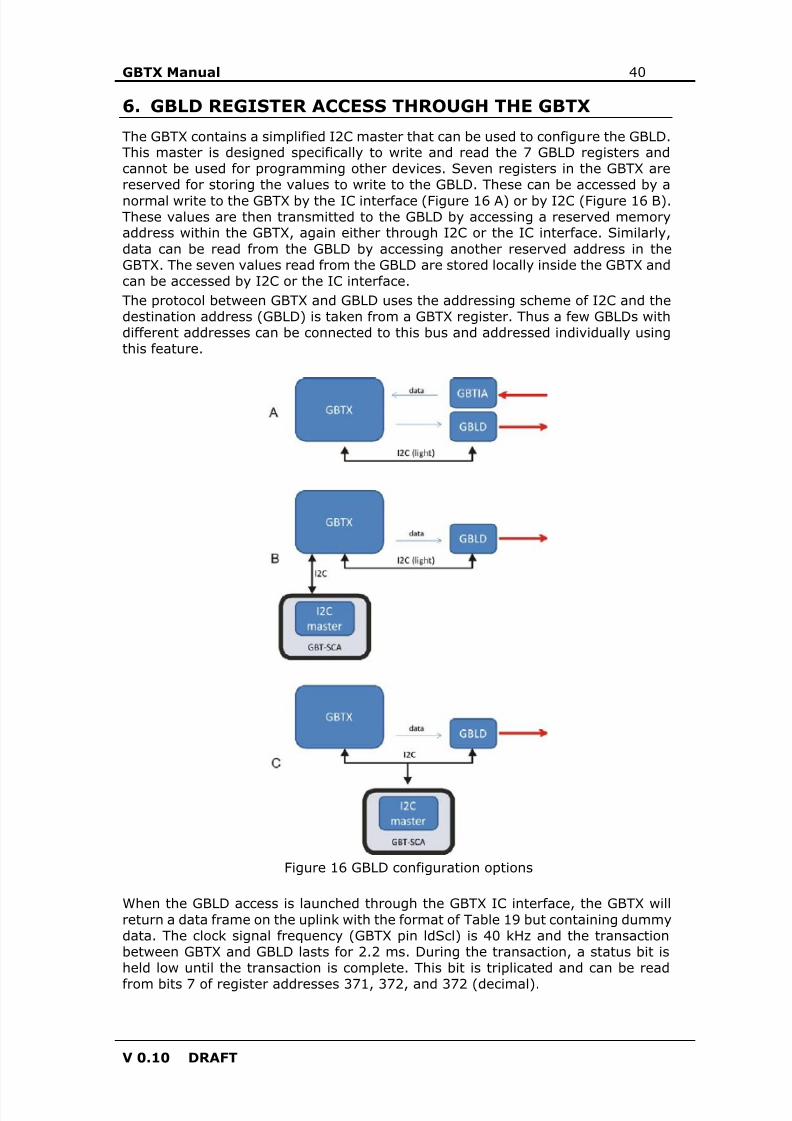
8/15/2019 gbtx Manual
http://slidepdf.com/reader/full/gbtx-manual 40/200
GBTX Manual 40
V 0.10 DRAFT
6. GBLD REGISTER ACCESS THROUGH THE GBTX
The GBTX contains a simplified I2C master that can be used to configure the GBLD.This master is designed specifically to write and read the 7 GBLD registers andcannot be used for programming other devices. Seven registers in the GBTX arereserved for storing the values to write to the GBLD. These can be accessed by anormal write to the GBTX by the IC interface (Figure 16 A) or by I2C (Figure 16 B).These values are then transmitted to the GBLD by accessing a reserved memoryaddress within the GBTX, again either through I2C or the IC interface. Similarly,data can be read from the GBLD by accessing another reserved address in theGBTX. The seven values read from the GBLD are stored locally inside the GBTX andcan be accessed by I2C or the IC interface.The protocol between GBTX and GBLD uses the addressing scheme of I2C and thedestination address (GBLD) is taken from a GBTX register. Thus a few GBLDs withdifferent addresses can be connected to this bus and addressed individually usingthis feature.
Figure 16 GBLD configuration options
When the GBLD access is launched through the GBTX IC interface, the GBTX willreturn a data frame on the uplink with the format of Table 19 but containing dummydata. The clock signal frequency (GBTX pin ldScl) is 40 kHz and the transactionbetween GBTX and GBLD lasts for 2.2 ms. During the transaction, a status bit isheld low until the transaction is complete. This bit is triplicated and can be readfrom bits 7 of register addresses 371, 372, and 372 (decimal).
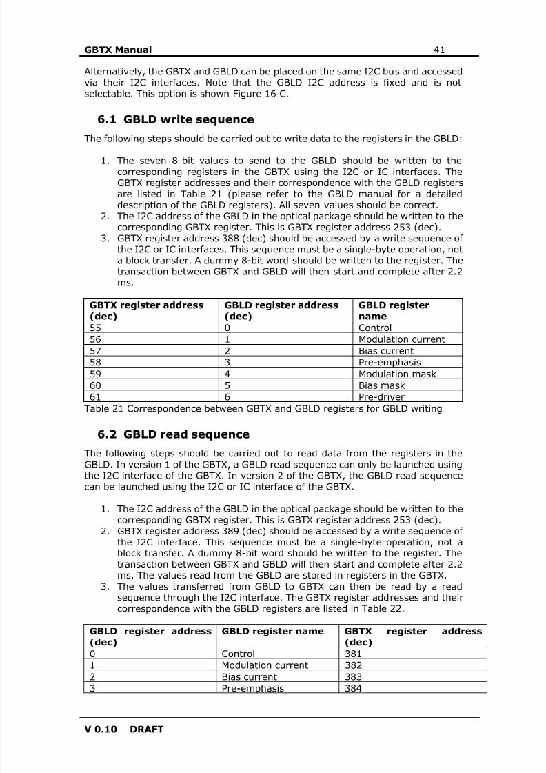
8/15/2019 gbtx Manual
http://slidepdf.com/reader/full/gbtx-manual 41/200
GBTX Manual 41
V 0.10 DRAFT
Alternatively, the GBTX and GBLD can be placed on the same I2C bus and accessedvia their I2C interfaces. Note that the GBLD I2C address is fixed and is notselectable. This option is shown Figure 16 C.
6.1 GBLD write sequence
The following steps should be carried out to write data to the registers in the GBLD:
1. The seven 8-bit values to send to the GBLD should be written to thecorresponding registers in the GBTX using the I2C or IC interfaces. TheGBTX register addresses and their correspondence with the GBLD registersare listed in Table 21 (please refer to the GBLD manual for a detaileddescription of the GBLD registers). All seven values should be correct.
2. The I2C address of the GBLD in the optical package should be written to thecorresponding GBTX register. This is GBTX register address 253 (dec).
3. GBTX register address 388 (dec) should be accessed by a write sequence ofthe I2C or IC interfaces. This sequence must be a single-byte operation, nota block transfer. A dummy 8-bit word should be written to the register. Thetransaction between GBTX and GBLD will then start and complete after 2.2ms.
GBTX register address(dec)
GBLD register address(dec)
GBLD registername
55 0 Control56 1 Modulation current57 2 Bias current58 3 Pre-emphasis59 4 Modulation mask60 5 Bias mask61 6 Pre-driver
Table 21 Correspondence between GBTX and GBLD registers for GBLD writing
6.2 GBLD read sequence
The following steps should be carried out to read data from the registers in theGBLD. In version 1 of the GBTX, a GBLD read sequence can only be launched usingthe I2C interface of the GBTX. In version 2 of the GBTX, the GBLD read sequencecan be launched using the I2C or IC interface of the GBTX.
1. The I2C address of the GBLD in the optical package should be written to thecorresponding GBTX register. This is GBTX register address 253 (dec).
2. GBTX register address 389 (dec) should be accessed by a write sequence of
the I2C interface. This sequence must be a single-byte operation, not ablock transfer. A dummy 8-bit word should be written to the register. Thetransaction between GBTX and GBLD will then start and complete after 2.2ms. The values read from the GBLD are stored in registers in the GBTX.
3. The values transferred from GBLD to GBTX can then be read by a readsequence through the I2C interface. The GBTX register addresses and theircorrespondence with the GBLD registers are listed in Table 22.
GBLD register address(dec)
GBLD register name GBTX register address(dec)
0 Control 3811 Modulation current 382
2 Bias current 3833 Pre-emphasis 384
8/15/2019 gbtx Manual
http://slidepdf.com/reader/full/gbtx-manual 42/200
GBTX Manual 42
V 0.10 DRAFT
4 Modulation mask 3855 Bias mask 3866 Pre-driver 387
Table 22: Correspondence between GBLD and GBTX registers for GBLD reading
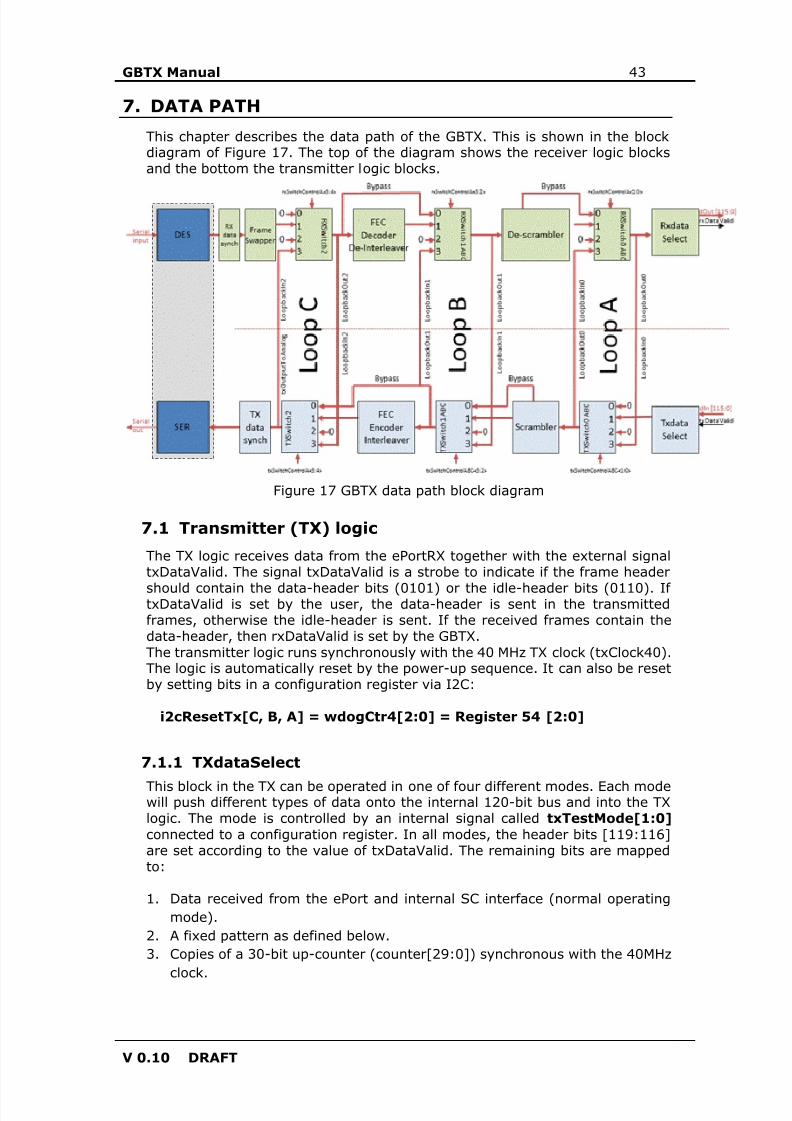
8/15/2019 gbtx Manual
http://slidepdf.com/reader/full/gbtx-manual 43/200
GBTX Manual 43
V 0.10 DRAFT
7. DATA PATH
This chapter describes the data path of the GBTX. This is shown in the blockdiagram of Figure 17. The top of the diagram shows the receiver logic blocksand the bottom the transmitter logic blocks.
Figure 17 GBTX data path block diagram
7.1 Transmitter (TX) logic
The TX logic receives data from the ePortRX together with the external signaltxDataValid. The signal txDataValid is a strobe to indicate if the frame header
should contain the data-header bits (0101) or the idle-header bits (0110). IftxDataValid is set by the user, the data-header is sent in the transmittedframes, otherwise the idle-header is sent. If the received frames contain thedata-header, then rxDataValid is set by the GBTX.The transmitter logic runs synchronously with the 40 MHz TX clock (txClock40).The logic is automatically reset by the power-up sequence. It can also be resetby setting bits in a configuration register via I2C:
i2cResetTx[C, B, A] = wdogCtr4[2:0] = Register 54 [2:0]
7.1.1 TXdataSelect
This block in the TX can be operated in one of four different modes. Each modewill push different types of data onto the internal 120-bit bus and into the TXlogic. The mode is controlled by an internal signal called txTestMode[1:0] connected to a configuration register. In all modes, the header bits [119:116]are set according to the value of txDataValid. The remaining bits are mappedto:
1. Data received from the ePort and internal SC interface (normal operatingmode).
2. A fixed pattern as defined below.3. Copies of a 30-bit up-counter (counter[29:0]) synchronous with the 40MHz
clock.
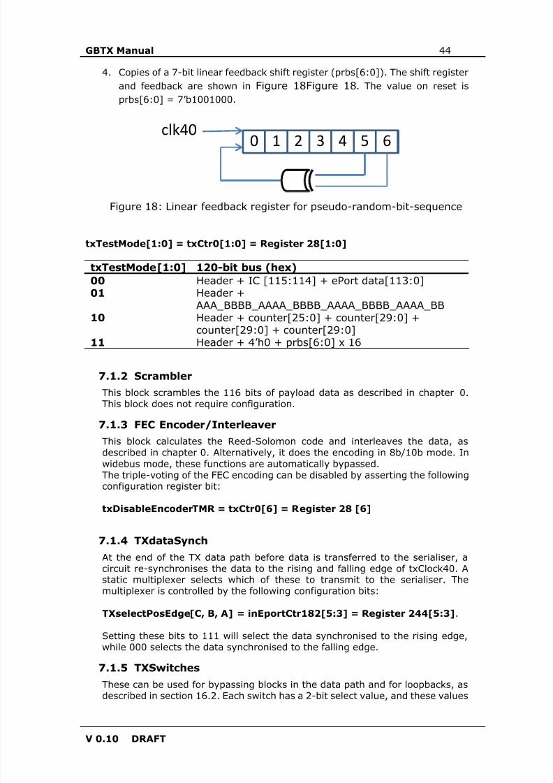
8/15/2019 gbtx Manual
http://slidepdf.com/reader/full/gbtx-manual 44/200
GBTX Manual 44
V 0.10 DRAFT
4. Copies of a 7-bit linear feedback shift register (prbs[6:0]). The shift registerand feedback are shown in Figure 18Figure 18 . The value on reset isprbs[6:0] = 7’b1001000.
Figure 18: Linear feedback register for pseudo-random-bit-sequence
txTestMode[1:0] = txCtr0[1:0] = Register 28[1:0]
txTestMode[1:0] 120-bit bus (hex)00 Header + IC [115:114] + ePort data[113:0]01 Header +
AAA_BBBB_AAAA_BBBB_AAAA_BBBB_AAAA_BB10 Header + counter[25:0] + counter[29:0] +
counter[29:0] + counter[29:0]11 Header + 4’h0 + prbs[6:0] x 16
7.1.2 Scrambler
This block scrambles the 116 bits of payload data as described in chapter 0. This block does not require configuration.
7.1.3 FEC Encoder/Interleaver
This block calculates the Reed-Solomon code and interleaves the data, asdescribed in chapter 0. Alternatively, it does the encoding in 8b/10b mode. Inwidebus mode, these functions are automatically bypassed.The triple-voting of the FEC encoding can be disabled by asserting the followingconfiguration register bit:
txDisableEncoderTMR = txCtr0[6] = Register 28 [6]
7.1.4 TXdataSynch
At the end of the TX data path before data is transferred to the serialiser, acircuit re-synchronises the data to the rising and falling edge of txClock40. Astatic multiplexer selects which of these to transmit to the serialiser. Themultiplexer is controlled by the following configuration bits:
TXselectPosEdge[C, B, A] = inEportCtr182[5:3] = Register 244[5:3] .
Setting these bits to 111 will select the data synchronised to the rising edge,while 000 selects the data synchronised to the falling edge.
7.1.5 TXSwitches
These can be used for bypassing blocks in the data path and for loopbacks, asdescribed in section 16.2. Each switch has a 2-bit select value, and these values
clk40
0 1 2 3 4 5 6
8/15/2019 gbtx Manual
http://slidepdf.com/reader/full/gbtx-manual 45/200
GBTX Manual 45
V 0.10 DRAFT
are stored in the following configuration registers. The different selectable pathsand their corresponding bits in the registers are shown in Figure 17 and aregiven in Table 23, Table 24 and Table 25.
txSwitchesControlA[7:0] = txCtr1[7:0] = Register 29 [7:0]txSwitchesControlB[7:0] = txCtr2[7:0] = Register 30 [7:0]txSwitchesControlC[7:0] = txCtr3[7:0] = Register 31 [7:0]
Table 23 TX switch 0 mapping
TX Switch 0txSwitchesControlA/B/C[1:0]=Register 29/30/31 [1:0]
Switch input
2’b00 120’h0000000000000000000000000000002’b01 Header + IC [115:114] + Eport data[113:0]2’b10 120’h000000000000000000000000000000
2’b11 RX Switch 0 output
Table 24 TX switch 1 mapping
TX Switch 1txSwitchesControlA/B/C[3:2]=Register 29/30/31 [3:2]
Switch input
2’b00 TX Switch 0 output followed by one stagepipeline delay (txClock40)
2’b01 Scrambler output
2’b10 120’h0000000000000000000000000000002’b11 RX Switch 1 output
Table 25 TX switch 2 mapping
TX Switch 2txSwitchesControlA/B/C[5:4]=Register 29/30/31 [5:4]
Switch input
2’b00 TX Switch 1 output2’b01 FEC encoder interleaver output2’b10 120’h0000000000000000000000000000002’b11 RX Switch 2 output
7.2 Receiver (RX) logic
The RX logic receives data from the deserialiser. If the received frame containsthe data-header (0101), then rxDataValid is set high by the GBTX. If the framecontains the idle-header (0110), then rxDataValid is low.The receiver core logic runs synchronously with the 40 MHz RX clock(rxClock40).The logic is automatically reset by the power-up sequence. It can also be resetby setting bits in a configuration register via I2C:
i2cResetRx[C, B, A] = wdogCtr0[5:3] = Register 50 [5:3]
8/15/2019 gbtx Manual
http://slidepdf.com/reader/full/gbtx-manual 46/200
8/15/2019 gbtx Manual
http://slidepdf.com/reader/full/gbtx-manual 47/200
GBTX Manual 47
V 0.10 DRAFT
11 = x 8 0111111101111111 = 16’h7F7F
A 16-bit error-counter is also included in this block. It will compare the datareceived from the RX logic (bits [115:32] of the frame) and compares themwith the fixed pattern:[115:32] = AAA_BBBB_AAAA_BBBB_AAAA_BB
The counter is enabled by the internal signals enableBERT_ABC connected to aconfiguration register:
enableBERT[C, B, A] = rxCtr14[4:2] = Register 49[4:2]
The counter is zeroed by turning on the enable bits. The 16-bit counter valuecan be read via the I2C or IC interfaces by reading registers 369 (counter[7:0])and 370 (counter[15:8]). Notice that the counter will roll over to zero if a wrongword is detected when the counter had already reached the end count.
7.2.6 RXSwitches
These can be used for bypassing blocks in the data path and for loopbacks, asdescribed in section 16.2. Each switch has a 2-bit select value, and these valuesare stored in the following configuration registers. The different selectable pathsand their corresponding bits in the registers are shown in Figure 17 and aregiven in Table 26, Table 27 and Table 28.
rxSwitchesControlA[7:0] = rxCtr11[7:0] = Register 46 [7:0]rxSwitchesControlB[7:0] = rxCtr12[7:0] = Register 47 [7:0]rxSwitchesControlC[7:0] = rxCtr13[7:0] = Register 48 [7:0]
Table 26 RX switch 0 mapping
RX Switch 0rxSwitchesControlA/B/C[1:0]=Register 46/47/48 [1:0]
Switch input
2’b00 RX switch 1 output followed by one stagepipeline delay (rxClock40)
2’b01 De-scrambler output2’b10 120’h0000000000000000000000000000002’b11 TX switch 1 output
Table 27 RX switch 1 mapping
RX Switch 1rxSwitchesControlA/B/C[3:2]=Register 46/47/48 [3:2]
Switch input
2’b00 RX switch 2 output2’b01 FEC decoder and de-interleaver output2’b10 120’h0000000000000000000000000000002’b11 TX switch 1 output
Table 28 RX switch 2 mapping
RX Switch 2
8/15/2019 gbtx Manual
http://slidepdf.com/reader/full/gbtx-manual 48/200
GBTX Manual 48
V 0.10 DRAFT
rxSwitchesControlA/B/C[5:4]=Register 46/47/48 [5:4]
Switch input
2’b00 120’h0000000000000000000000000000002’b01 Frame swapper output2’b10 120’h0000000000000000000000000000002’b11 TX switch 2 output
7.3 Summary of configuration inputs
The registers listed in Table 29 are used to configure the GBTX data path.
Table 29 Data path configuration registers
Register address Register name Bits
28 txCtr0 [1:0]
28 txCtr0 [6]244 inEportCtr182 [5:3]244 inEportCtr182 [2:0]49 rxCtr14 [1]49 rxCtr14 [7:5]49 rxCtr14 [4:2]29 txCtr1 [7:0]30 txCtr2 [7:0]31 txCtr3 [7:0]
46 rxCtr11 [7:0]47 rxCtr12 [7:0]48 rxCtr13 [7:0]54 wdogCtr4 [2:0]50 wdogCtr0 [5:3]
8/15/2019 gbtx Manual
http://slidepdf.com/reader/full/gbtx-manual 49/200
GBTX Manual 49
V 0.10 DRAFT
8. SLOW CONTROL CHANNEL (EC)
The two bit EC field of the GBT frame is available to implement a bidirectionalserial channel with a bandwidth of 80 Mb/s (if bidirectional link). This operatesan E-Link in the 2 x mode with an e-Clock of 40/80 MHz. The slow control pathis primarily intended to communicate with a GBT-SCA chip but can be used forother purposes. Conversely, the GBT-SCA can operate with any other ePortprovided that that port is operated as an E-Link in the 2 × mode.Note that for communication with the GBT-SCA, the e-Clock must be 40 MHz toallow dual-data-rate communication with the 80 Mb/s serial stream.
The following settings should be used to configure the E-link for communicatingwith the GBT-SCA.
EC DLL configuration A[3:0] = inEportCtr169[3:0] = Register 231[3:0]EC DLL configuration B[3:0] = inEportCtr169[7:4] = Register 231[7:4]EC DLL configuration C[3:0] = inEportCtr170[3:0] = Register 232[3:0]EC DLL reset ABC = inEportCtr170[6:4] = Register 232[6:4]EC DLL coarse-lock-detection ABC = inEportCtr171[6:4] = Register 233[6:4]
EC enable ABC = inEportCtr186[2:0] = Register 248[2:0]Phase aligner track mode A[1:0] = inEportCtr0[1:0] = Register 62[1:0]Phase aligner track mode B[1:0] = inEportCtr0[3:2] = Register 62[3:2]Phase aligner track mode C[1:0] = inEportCtr0[5:4] = Register 62[5:4]
EC channel reset ABC = inEportCtr189[2:0] = Register 251[2:0]EC channel train ABC = inEportCtr183[2:0] = Register 245[2:0]
EC sample phase select A[3:0] = inEportCtr171[3:0] = Register 233[3:0]EC sample phase select B[3:0] = inEportCtr175[3:0] = Register 237[3:0]EC sample phase select C[3:0] = inEportCtr179[3:0] = Register 241[3:0]
EC data rate mode ABC = outEportCtr0[6:4] = Register 254[5:4]Set to 3’b111 to select 80 Mb/s for the GBT-SCA
EC clock frequency ABC = outEportCtr3[6:4] = Register 257[6:4]Set to 3’b000 to select 40 MHz for the GBT-SCA
EC enable receiver termination = ckCtr4[5] = Register 273[5]EC driver current control [3:0] = ckCtr4[3:0] = Register 273[3:0]
8/15/2019 gbtx Manual
http://slidepdf.com/reader/full/gbtx-manual 50/200
GBTX Manual 50
V 0.10 DRAFT
9. ASIC OPERATION CONTROL
This chapter describes the control logic of the GBTX. In general, this carries out theinitialisation of a number of sub-blocks and subsequently monitors their status.Most of these status signals are feedback to the power-up state machine and thewatchdog (see chapter 10 for power-up and watchdog operation). The GBTconfiguration is loaded at power-on, or after a GBTX reset, from a bank ofelectrically programmable fuses (see chapter 15 for further details on e-Fuses).The fuses allow the GBTX to be optimized for specific applications already at thepower-up stage. The e-Fuse configuration data is programmed after productiontesting of the ASICs targeting specific user requirements . The settings of the e-Fuses are copied into the GBTX configuration registers (see chapter 16 for acomplete list of the GBTX registers) after which the GBTX will start its internalinitialization procedure according to the selected link mode (receiver, transmitteror transceiver).After appropriate initialization, the GBTX configuration can be modified via theoptical link itself, that is the IC channel (if used in transceiver mode), or via theI2C configuration interface. Monitoring of the GBT/link and read-back ofconfiguration data can also be performed via these two control interfaces.All configuration registers in the GBTX are clock gated (for low power consumption)and fully protected against SEU’s with triple redundant registers with auto errorrecovery.
9.1 Transceiver modes
External mode signals MODE [3:0] (see chapter 18 for pin numbers) define themost basic operation modes (see 1.3) and configuration of the GBT according tothe table below.
Table 30 Transceiver mode configuration signals
Encoding/Bus mode Transceiver mode MODE [3:0]
FEC Simplex TX 0000
FEC Simplex RX 0001
FEC Transceiver 0010
FEC Test 0011
WideBus Simplex TX 0100
WideBus Simplex RX 0101
WideBus Transceiver 0110
8/15/2019 gbtx Manual
http://slidepdf.com/reader/full/gbtx-manual 51/200
GBTX Manual 51
V 0.10 DRAFT
WideBus Test 0111
8b/10b Simplex TX 1000
8b/10b Simplex RX 1001
8b/10b Transceiver 1010
8b/10b Test 1011
(reserved) (reserved) 1100
(reserved) (reserved) 1101
(reserved) (reserved) 1110
(reserved) (reserved) 1111
9.2 TX control
This is a state-machine which initialises and monitors the status of the serialiser.It monitors the locked status of the serialiser PLL, and if this is stable for longerthan a specified time (see txPllLockTime in Table 31) then it signals the power-up state-machine/watchdog that the serialiser is locked and operational. It willsignal that the serialiser has lost lock either immediately or only if lock is lostfor longer than a specified time if soft-loss-of-lock is enabled (seetxLossOfLockTime in Table 31) . Soft-loss-of-lock is enabled by writing a 1’b1 inbit 6 of register 33:
Register 33[6] = txCtr5[6] = txEnableSoftLossOfLock
When lock is lost, the TX Loss of Lock Counter will increment. The contents ofthe counter can be read through I2C or SC-IC. The counter is only reset by thepower-on-reset or external reset. The loss of lock count can be read fromregister 376:
Register 376[7:0] = txLossOfLockCount[7:0]
The output of the control block can be forced into the “locked” state via I2C orSC-IC by writing into bit 4 of register 32:
Register 32[4] = txForceLockState
The block is automatically reset at power-up and by the external reset. It canalso be reset by writing into configuration register 33 via I2C.
Register 33[2:0] = txCtr5[2:0] = i2cTxReset[C, B, A]
8/15/2019 gbtx Manual
http://slidepdf.com/reader/full/gbtx-manual 52/200
GBTX Manual 52
V 0.10 DRAFT
A reset through the I2C requires bits i2cTxReset[C, B, A] to be set and thencleared.
The TX control configurable parameters are listed in Table 31.
Table 31 TX control parameters
Parameter Register Bits FunctiontxPllLockTime 32 = txCtr4 [3:0] Sets number of cycles that serialiser PLL must stay
locked before TXcontrol asserts locked state.Number of cycles = 2 ^ txPllLockTime.Maximum value = 9 (dec).
txLossOfLockTime 32 = txCtr4 [7:5] Sets number of cycles for which serialiser PLLshould be unlock before TXcontrol de-assertslocked state.Only active if soft-loss-of-lock is enabled.Number of cycles = 2 ^ txLossOfLockTime.Maximum value = 4 (dec).
txEnableSoftLossOfLock 33 = txCtr5 [6] Enables the soft-loss-lock.txForceLockState 32 = txCtr4 [4] Forces TX control to assert the locked state.i2cTxReset[C, B, A] 33 = txCtr5 [2:0] Resets TX control
9.3 RX control
The RX Control State Machine (RXCSM) controls the operation of the receiversection of the GBTX. The receiver is divided in two main circuits: the Clock andData Recovery (CDR) circuit and the Frame Aligner (FA) circuit. The CDRfunction is further subdivided into Frequency Locking (FL) and Phase Locking (PL) functions. The block diagrams of the CDR and FA circuits are representedin Figure 19 and Figure 20 respectively.
9.3.1 Clock and Data RecoveryFor the 4.8 Gb/s serial data stream to be correctly received by the GBTX boththe frequency and phase of the de-serializer clock (CDR clock) need to matchprecisely the carrier frequency and phase of the incoming data. In the case ofthe GBTX an Half-Rate (HR) CDR architecture is used which results (in the CDRcircuit) in a 180 degree phase ambiguity that is resolved later in the receivingchain with the help of the frame aligner circuit (see Frame Aligner) .CDR is achieved in the GBTX by a two stage process. In the first phase thefrequency of the CDR PLL is pulled close to 2.4 GHz (“half data rate” clock)either by an auxiliary PLL, locked to a reference 40 MHz clock, or by a
“calibration” DAC under the control of a frequency calibration state machine. Inthe second phase, after completion of frequency calibration, the CDR loop isenabled and the CDR PLL locks to the frequency and phase of the incoming datastream (see 9.3.2) .The locking procedure is fully controlled by the RX Control State Machine(RXCSM) without user intervention. However, it is also possible to fully controlthe lock procedure through the I2C interface. This option is however strictlyreserved for test purposes only.
9.3.1.1 Lock mode selection
The different locking modes mentioned above, are selected by the pinsRXLOCKMODE [1:0] according to Table 32 (see chapter 18 for pin numbers).
8/15/2019 gbtx Manual
http://slidepdf.com/reader/full/gbtx-manual 53/200
GBTX Manual 53
V 0.10 DRAFT
Table 32 Receiver lock mode configuration signals
RXLOCKMODE [1:0] Receiver lock mode2’b00 I2C frequency calibration2’b01 Automatic DAC frequency calibration
2’b10 Automatic Reference PLL frequencycalibration2’b11 (reserved)
9.3.2 CDR Circuit Architecture and Operation
The architecture of the CDR circuit is shown in Figure 20 . There it can be seenthat the CDR PLL receives a coarse tuning voltage that centres the CDR PLLVCO frequency around 2.4 GHz. This voltage is provided either from thereference PLL or from the DAC. A few switches are responsible for the sourceselection:
1. The DAC switch allows the DAC to drive the coarse tuning voltage and isenabled / disabled by the signals rxDacEnable[C, B, A] . When these
switches are enabled the DAC controls the coarse tuning voltage.Whenever the REF PLL is used to control the coarse voltage theseswitches must be disabled.
2. The coarse voltage can be driven by the reference PLL when either theLow-Pass Filter (LPF) is enabled rxFilterEnable[C, B, A] = 3’b111 or whenthe filter is bypassed rxFilterBipass[C, B, A] = 3’b111 . Whenever theDAC is used to control the coarse voltage both switches must be open.
The CDR switches are automatically controlled by the Lock Control StateMachine (LCSM). However, for testing purposes, these switches can becontrolled through the I2C interface. This requires the user to set the mode pinsto RXLOCKMODE[1:0] = 2’b00 or the signals i2cRxControlOverride[C, B, A] =3’b111 before the contents of registers 42 to 45 can have any effect on theGBTX operation (see Table 42 to Table 46 for details). This last option is givenonly for ASIC test purposes; the user is strongly discouraged from trying tocontrol the CDR function through the I2C interface.
Figure 19 Clock and Data Recovery circuit block diagram
8/15/2019 gbtx Manual
http://slidepdf.com/reader/full/gbtx-manual 54/200
GBTX Manual 54
V 0.10 DRAFT
9.3.2.1 Rx Frequency Centring
Depending on the lock mode ( RXLOCKMODE [1:0] ) the lock control state machinewill select either the REF PLL or the DAC for frequency centring. In both cases untilthe frequency centring process is concluded, the fine and coarse control voltagesof the CDR VCO are shorted together and the CDR loop has no control over the
VCO frequency. This is done by asserting signal rxForceVfEqVc[C, B, A] = 3’b111and setting the phase and frequency detectors charge pumps currents to zero. Allthis is made under the supervision of the LCSM without user intervention. However,for testing purposes, this can be controlled through the I2C interface by the signalsi2cRxForceVfEqVc[C, B, A] .When the I2C control is enabled ( i2cRxControlOverride[C, B, A] = 3’b111 orRXLOCKMODE [1:0] = 2’b00) the DAC can also be controlled through the I2Cinterface through the signals rxDacGain and i2cRxDac [8:0] . The former signal setsthe DAC range (high/low) and the latter is the DAC count to be digital-to-analogueconverted (see Table 35, Table 38 and Table 43) . When enabled, the DAC drivesthe coarse tuning voltage and thus controls the CDR VCO centre frequency.Notice that the signal rxDacGain is a configuration setting signal. It is always activein lock modes 2’b00 and 2’b01 (provided the DAC is enabled) independently of thestate of signal i2cRxControlOverride[C, B, A] .
Frequency centring is complete when the REF PLL has acquired lock(RXLOCKMODE [1:0] = 2’b10) or the lock control state machine has concluded abinary search process to calibrate the CDR VCO frequency ( RXLOCKMODE [1:0] =2’b01). In the automatic DAC frequency calibration mode, the LCSM uses two 11-bit counters to compare the frequency of the CDR VCO (divided by 60) to thefrequency of the reference clock. During a binary search cycle the two counters aresimultaneously reset and then allowed to count up till one of them reaches the “endcount”. One of the counters runs with the reference clock (40 MHz) and is calledreferenceFast and the other, vcoFast , runs with the RX clock rxClock40 . Whichevercounter reaches the end count first gives an indication to the state machine if theCDR VCO clock frequency is high or low in relation to the reference clock. Whenrunning the locking process under the I2C control, there are a few registers thatcan be used to control the referenceFast and vcoFast counters and to verify thestatus of the frequency comparison, these are:
1. Signal i2cStartRace[C, B, A] = Register 42 [2:0] used to enable and clearthe race counters: referenceFast and vcoFast . Setting this bits to “3’b000”clears the race counters and setting them to “3’b111” enables the counters(see Table 41) .
2. Signal vcoFast = Register 377 [1] reports the result of the frequency racecounters (see Table 47) . When bit Register 377 [1] is read, if the returnedvalue is “1’b0” this indicates that the reference frequency is higher than theVCO frequency, if it is “1’b1” it means that the VCO frequency is higher thanthe reference frequency. Notice that there is no flag indicating that a
“frequency race” is complete. Because of this, when controlling the “race”counters through I2C, enough time must be allowed between enabling the
“race’ counters and reading the status bit Register 377 [1] . The minimumwaiting time is 110 ms.
9.3.2.2 Rx Phase Locking
When the frequency centring process is concluded, the CDR loop enters a phase-frequency locking procedure. This is enabled by setting rxForceVfEqVc[C, B, A] =3’b000 and by enabling the CDR charge-pump currents. The CDR loop will be thenpulled in frequency and phase until it locks to the incoming data. As mentionedbefore phase locking with an half rate CDR architecture has an intrinsic 180 degreephase ambiguity of the recovered clock. The control signalrxSelectDataInPhase[C, B, A] is used to resolve that ambiguity and guarantee that
8/15/2019 gbtx Manual
http://slidepdf.com/reader/full/gbtx-manual 55/200
GBTX Manual 55
V 0.10 DRAFT
the GBTX clock and data can be recovered with no phase ambiguity and thus theASIC will always display constant latency. The signals rxSelectDataInPhase[C, B, A] are under the control of the RX Control State Machine (RXCSM) as explained laterwhen the frame aligner will be discussed (section 9.3.3) .When I2C control is enabled these signals can be controlled by signali2cRxSelectDataInPhase[C, B, A] = Register 36[5:3] (see Table 39) .The loop parameters of the CDR and Reference PLL are controlled by the contentsof registers 34, 35 and 41 as indicated in Table 36, Table 37 and Table 40. Theseregisters are always active independently of the lock mode. However, duringfrequency centring the charge-pump currents of the CDR loop are overwritten (setto zero) by the lock control state machine.
Table 33 Reference PLL filter resistor selection
rxSelectR[1:0] = Register 34 [1:0] Reference PLL filter resistor2’b00 500 Ω 2’b01 700 Ω
2’b10 1000 Ω 2’b11 2000 Ω
Table 34 CDR PLL filter resistor selection
rxSelectR[3:2] = Register 34 [3:2] CDR PLL filter resistor2’b00 500 Ω 2’b01 700 Ω 2’b10 1000 Ω 2’b11 2000 Ω
Table 35 Signal rxDacGain[C, B, A]
rxDacGain[C, B, A] = Register 34 [6:4] DAC voltage range3’b000 570 mV to 640 mV3’b111 590 mV to 710 mVOther combinations are invalid n.a.
Table 36 CDR frequency detector charge pump current selection
i2cRxSelectI2[3:0] = Register 35 [3:0] CDR frequency detectorcharge pump current [ A]
4’bxxxx I = 0.375 × i2cRxSelectI2[3:0]
Table 37 CDR phase detector charge pump current selection
i2cRxSelectI2[7:4] = Register 35 [7:4] CDR phase detector chargepump current [ A]
4’bxxxx I = 0.375 × i2cRxSelectI2[7:4]
Table 38 Signal i2cRxControlOverride[C, B, A] function
i2cRxControlOverride[C, B, A] =Register 36 [2:0]
I2C control
3’b000 Disabled3’b111 Enabled
8/15/2019 gbtx Manual
http://slidepdf.com/reader/full/gbtx-manual 56/200
GBTX Manual 56
V 0.10 DRAFT
Other combinations are invalid n.a.
Table 39 Signal i2cRxSelectDataInPhase (valid only ifi2cRxControlOverride[C, B, A] = 3’b111 or RXLOCKMODE [1:0] = 2’b00)
i2cRxSelectDataInPhase[C, B, A] =Register 36 [5:3] CDR data phase selection
3’b000 Select data in anti-phase3’b111 Select In phase dataOther combinations are invalid n.a.
Table 40 Reference PLL charge-pump current selection
i2cRxSelectI1[7:4] = Register 41 [7:4] Reference PLL charge pumpcurrent [ A]
4’bxxxx I = 6.67 × i2cRxSelectI1[7:4]
Table 41 Signal i2cStartRace[C, B, A] (valid only ifi2cRxControlOverride[C, B, A] = 3’b111 or RXLOCKMODE [1:0] = 2’b00)
i2cStartRace[C, B, A] =Register 42 [2:0]
Race counters action
3’b000 Clear “race” counters3’b111 Enable “race” countersOther combinations are invalid n.a.
Table 42 Signal i2cRxDacEnable[C, B, A] function (valid only ifi2cRxControlOverride[C, B, A] = 3’b111 or RXLOCKMODE [1:0] = 2’b00)
i2cRxDacEnable[C, B, A] =Register 42 [5:3]
DAC state
3’b000 disabled3’b111 EnabledOther combinations are invalid n.a.
Table 43 Signal i2cRxDac [8:0] (valid only if i2cRxControlOverride[C, B, A] =3’b111 or RXLOCKMODE [1:0] = 2’b00)
i2cRxDac [8:0] = Register 44 [0],
Register 43 [7:0]
DAC output voltage
If rxDacGain = 1’b0 570 mV to 640 mVIf rxDacGain = 1’b1 590 mV to 710 mV
Table 44 Signal i2cRxFilterBypass[C, B, A] function (valid only ifi2cRxControlOverride[C, B, A] = 3’b111 or RXLOCKMODE [1:0] = 2’b00)
i2cRxFilterBypass[C, B, A] =Register 44 [3:1]
Low-Pass Filter bypass
3’b000 Disabled3’b111 EnabledOther combinations are invalid n.a.
8/15/2019 gbtx Manual
http://slidepdf.com/reader/full/gbtx-manual 57/200
GBTX Manual 57
V 0.10 DRAFT
Table 45 Signal i2cRxFilterEnable[C, B, A] function (valid only ifi2cRxControlOverride[C, B, A] = 3’b111 or RXLOCKMODE [1:0] = 2’b00)
i2cRxFilterEnable[C, B, A] =Register 45 [2:0]
Low-Pass Filter
3’b000 Disabled3’b111 EnabledOther combinations are invalid n.a.
Table 46 Signal i2cRxForceVfEqVc[C, B, A] function (valid only ifi2cRxControlOverride[C, B, A] = 3’b111 or RXLOCKMODE [1:0] = 2’b00)
i2cRxForceVfEqVc[C, B, A] =Register 45 [5:3]
V fine
3’b000 Under the CDR loop control3’b111 Shorted to V coarse Other combinations are invalid n.a.
Table 47 Race status bit “vcoFast”
vcoFast = Register 377 [1] Race status1’b0 VCO frequency low1’b1 VCO frequency high
9.3.3 Frame Aligner
The CDR circuit (see 9.3.2) recovers the clock and the serial data at half-rate,that is, the recovered clock frequency is 2.4 GHz ( clock2400MHz ) and two data
serial streams at 2.4 Gb/s ( dataPh0 and dataPh180 ) are recovered from theoriginal 4.8 Gb/s data stream. The CDR circuit is followed by the Frame Aligner (FA) circuit (see Figure 20 for a block diagram) whose function is to resolve the180 degree phase ambiguity of the recovered clock and to further de-serializethe two 2.4 Gb/s data streams recovered by the CDR circuit and assemble theminto a single 120-bit word (frame).
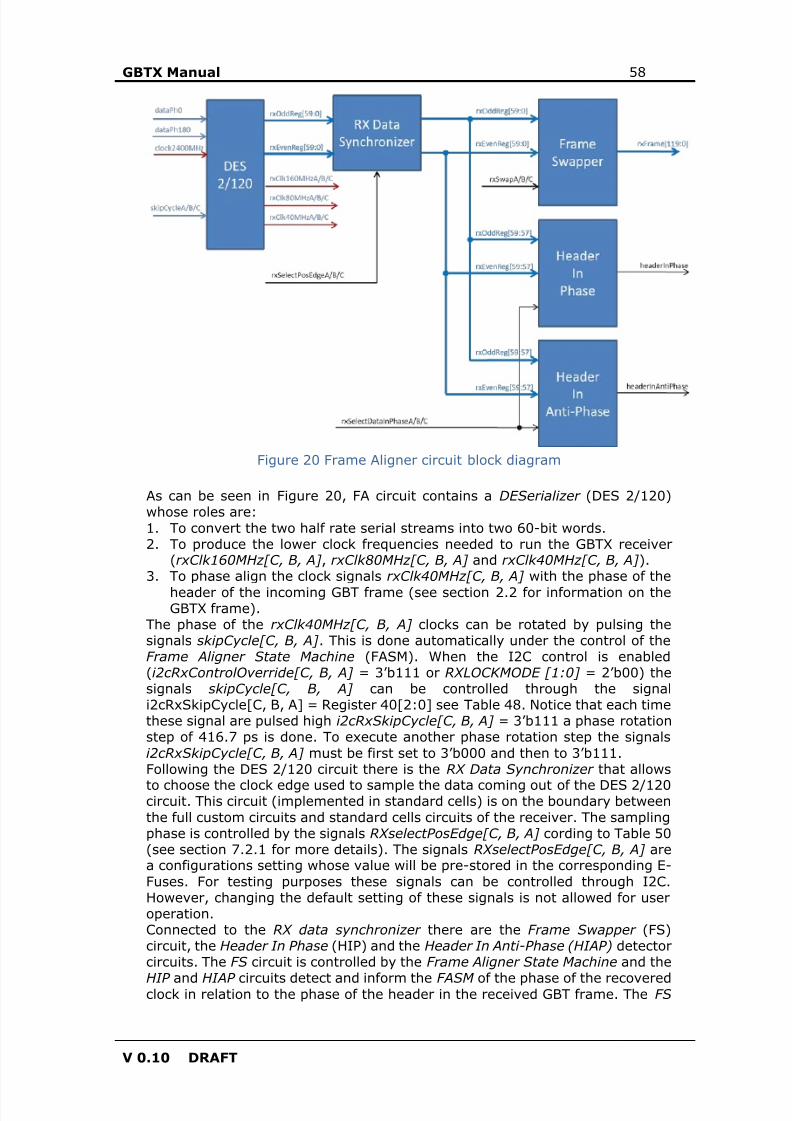
8/15/2019 gbtx Manual
http://slidepdf.com/reader/full/gbtx-manual 58/200
GBTX Manual 58
V 0.10 DRAFT
Figure 20 Frame Aligner circuit block diagram
As can be seen in Figure 20, FA circuit contains a DESerializer (DES 2/120)whose roles are:1. To convert the two half rate serial streams into two 60-bit words.2. To produce the lower clock frequencies needed to run the GBTX receiver
( rxClk160MHz[C, B, A] , rxClk80MHz[C, B, A] and rxClk40MHz[C, B, A] ).3. To phase align the clock signals rxClk40MHz[C, B, A] with the phase of the
header of the incoming GBT frame (see section 2.2 for information on theGBTX frame).
The phase of the rxClk40MHz[C, B, A] clocks can be rotated by pulsing thesignals skipCycle[C, B, A] . This is done automatically under the control of theFrame Aligner State Machine (FASM). When the I2C control is enabled( i2cRxControlOverride[C, B, A] = 3’b111 or RXLOCKMODE [1:0] = 2’b00) thesignals skipCycle[C, B, A] can be controlled through the signali2cRxSkipCycle[C, B, A] = Register 40[2:0] see Table 48. Notice that each timethese signal are pulsed high i2cRxSkipCycle[C, B, A] = 3’b111 a phase rotationstep of 416.7 ps is done. To execute another phase rotation step the signalsi2cRxSkipCycle[C, B, A] must be first set to 3’b000 and then to 3’b111.Following the DES 2/120 circuit there is the RX Data Synchronizer that allows
to choose the clock edge used to sample the data coming out of the DES 2/120circuit. This circuit (implemented in standard cells) is on the boundary betweenthe full custom circuits and standard cells circuits of the receiver. The samplingphase is controlled by the signals RXselectPosEdge[C, B, A] cording to Table 50(see section 7.2.1 for more details). The signals RXselectPosEdge[C, B, A] area configurations setting whose value will be pre-stored in the corresponding E-Fuses. For testing purposes these signals can be controlled through I2C.However, changing the default setting of these signals is not allowed for useroperation.Connected to the RX data synchronizer there are the Frame Swapper (FS)circuit, the Header In Phase (HIP) and the Header In Anti-Phase (HIAP) detectorcircuits. The FS circuit is controlled by the Frame Aligner State Machine and the
HIP and HIAP circuits detect and inform the FASM of the phase of the recoveredclock in relation to the phase of the header in the received GBT frame. The FS
8/15/2019 gbtx Manual
http://slidepdf.com/reader/full/gbtx-manual 59/200
GBTX Manual 59
V 0.10 DRAFT
circuit is controlled by the signals rxSwap[C, B, A] that are under the control ofthe FASM . When the I2C control is enabled ( i2cRxControlOverride[C, B, A] =3’b111 or RXLOCKMODE [1:0] = 2’b00) these signals are controlled throughthe I2C interface according to Table 49
Table 48 Signal i2cRxSkipCycle[C, B, A] (valid only ifi2cRxControlOverride[C, B, A] = 3’b111 or RXLOCKMODE [1:0] = 2’b00)
i2cRxSkipCycle[C, B, A] =Register 40 [2:0]
40 MHz RX clock
3’b000 Standby for the next phase shift3’b111 Single step 416.7ps phase shiftOther combinations are invalid n.a.
Table 49 Signal i2cRxSwap[C, B, A] (valid only ifi2cRxControlOverride[C, B, A] = 3’b111 or RXLOCKMODE [1:0] = 2’b00)
i2cRxSwap[C, B, A] =Register 40 [5:3]
Frame assembly
3’b000 rxOddReg[59:0] mapped intoodd bits of rxFrame[119:0] andrxEvenReg[59:0] mapped intoeven bits of rxFrame[119:0]
3’b111 rxOddReg[59:0] mapped intoeven bits of rxFrame[119:0]andrxEvenReg[59:0] mapped intoodd bits of rxFrame[119:0]
Other combinations are invalid n.a.
Table 50 RXselectPosEdge[C, B, A]
RXselectPosEdge[C, B, A] =Register 244 [2:0]
Data sampling
3’b000 On the falling edge3’b111 On the rising edgeOther combinations are invalid n.a.
9.3.3.1 Frame Aligner State Machine
The Frame Aligner State Machine ( FASM ) controls the locking process of GBTXreceiver. Its state flow diagram is represented in Figure 21 and Figure 22. Thestates can be generically divided into search states and tracking states. Thesearch states are entered at beginning of operation or when the FASM can’tidentify valid headers in the received frames. The tracking states keep track offrames with valid headers and, based on the locking phase, control the frameswapper for correct assembly of the frame. The FASM also controls the CDRclock phase to guarantee that the receiver displays constant latency every timethe CDR circuit locks to the incoming serial data. The tracking states implementa “robust” algorithm to avoid that either transmission errors or single eventupsets will unduly lead the FASM to enter the search states.
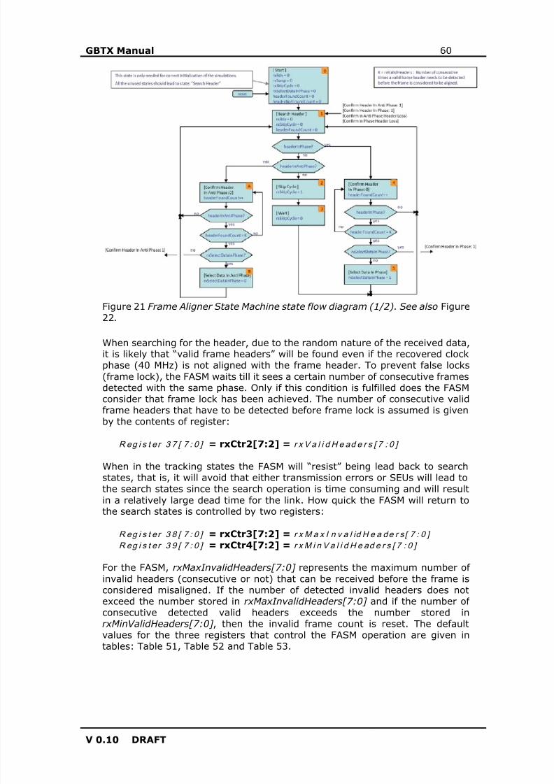
8/15/2019 gbtx Manual
http://slidepdf.com/reader/full/gbtx-manual 60/200
GBTX Manual 60
V 0.10 DRAFT
Figure 21 Frame Aligner State Machine state flow diagram (1/2). See also Figure22 .
When searching for the header, due to the random nature of the received data,it is likely that “valid frame headers” will be found even if the recovered clockphase (40 MHz) is not aligned with the frame header. To prevent false locks(frame lock), the FASM waits till it sees a certain number of consecutive framesdetected with the same phase. Only if this condition is fulfilled does the FASMconsider that frame lock has been achieved. The number of consecutive valid
frame headers that have to be detected before frame lock is assumed is givenby the contents of register:
R eg i s t e r 3 7 [ 7 : 0 ] = rxCtr2[7:2] = r x Va l i d H e ad e r s [ 7 : 0 ]
When in the tracking states the FASM will “resist” being lead back to searchstates, that is, it will avoid that either transmission errors or SEUs will lead tothe search states since the search operation is time consuming and will resultin a relatively large dead time for the link. How quick the FASM will return tothe search states is controlled by two registers:
R eg i s t e r 3 8 [ 7 : 0 ] = rxCtr3[7:2] = r x M a x I n v a l id H e a d e r s [ 7 : 0 ]
R eg i s t e r 3 9 [ 7 : 0 ] = rxCtr4[7:2] = r x M i n Va l i d H e ad e r s [ 7 : 0 ] For the FASM, rxMaxInvalidHeaders[7:0] represents the maximum number ofinvalid headers (consecutive or not) that can be received before the frame isconsidered misaligned. If the number of detected invalid headers does notexceed the number stored in rxMaxInvalidHeaders[7:0] and if the number ofconsecutive detected valid headers exceeds the number stored inrxMinValidHeaders[7:0] , then the invalid frame count is reset. The defaultvalues for the three registers that control the FASM operation are given intables: Table 51, Table 52 and Table 53.
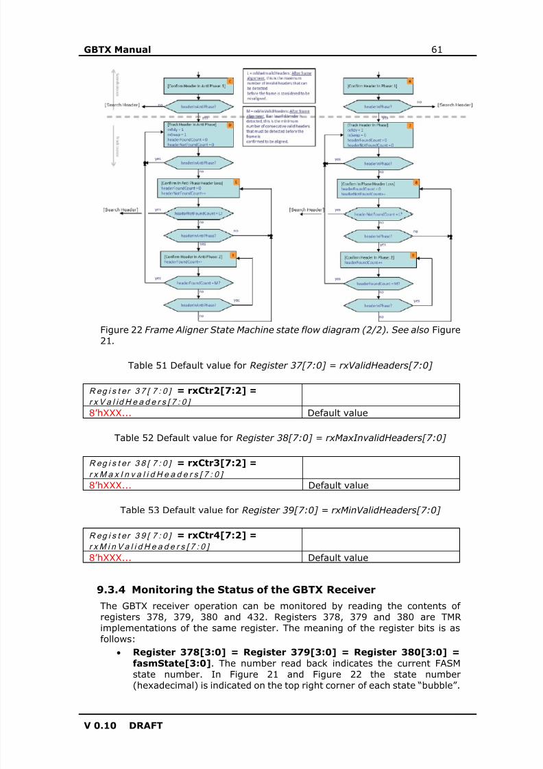
8/15/2019 gbtx Manual
http://slidepdf.com/reader/full/gbtx-manual 61/200
GBTX Manual 61
V 0.10 DRAFT
Figure 22 Frame Aligner State Machine state flow diagram (2/2). See also Figure21 .
Table 51 Default value for Register 37[7:0] = rxValidHeaders[7:0]
R eg i s t e r 3 7 [ 7 : 0 ] = rxCtr2[7:2] =
r x Va l id H e a d e r s [ 7 : 0 ] 8’hXXX... Default value
Table 52 Default value for Register 38[7:0] = rxMaxInvalidHeaders[7:0]
R eg i s t e r 3 8 [ 7 : 0 ] = rxCtr3[7:2] =r x M a x I n v a l i d H e a d e r s [ 7 : 0 ] 8’hXXX... Default value
Table 53 Default value for Register 39[7:0] = rxMinValidHeaders[7:0]
R eg i s t e r 3 9 [ 7 : 0 ] = rxCtr4[7:2] =r x M i n Va l i d H e a d e r s [ 7 : 0 ] 8’hXXX... Default value
9.3.4 Monitoring the Status of the GBTX Receiver
The GBTX receiver operation can be monitored by reading the contents ofregisters 378, 379, 380 and 432. Registers 378, 379 and 380 are TMRimplementations of the same register. The meaning of the register bits is asfollows:
• Register 378[3:0] = Register 379[3:0] = Register 380[3:0] =fasmState[3:0] . The number read back indicates the current FASMstate number. In Figure 21 and Figure 22 the state number(hexadecimal) is indicated on the top right corner of each state “bubble”.
8/15/2019 gbtx Manual
http://slidepdf.com/reader/full/gbtx-manual 62/200
GBTX Manual 62
V 0.10 DRAFT
• Register 378[4] = Register 379[4] = Register 380[4] =rxSkipCycle
• Register 378[5] = Register 379[5] = Register 380[5] =rxSelectDataInPhase
• Register 378[6] = Register 379[6] = Register 380[6] = rxSwap
• Register 378[7] = Register 379[7] = Register 380[7] =rxReady
9.3.5 Resetting the GBTX receiver
The GBTX receiver is reset at power-up or when the external reset is asserted.These are the two “standard” ways of resetting the receiver; the reset sequencefollows the steps indicated section 10.1. For testing purposes it is also possibleto reset the GBTX receiver under I2C control as detailed next.
9.3.5.1 Resetting the GBTX receiver through the I2C
The following registers can be used to reset the receiver through the I2Cinterface:
• Register 41[2:0] = rxCtr6[2:0] = i2cRxControlReset[C, B, A]• Register 50[5:3] = wdogCtr0[5:3] = i2cResetRx[C, B, A]• Register 53[1:0] = wdogCtr3[1:0] = i2cRxResetA[1:0]• Register 53[3:2] = wdogCtr3[3:2] = i2cRxResetB[1:0]• Register 53[5:4] = wdogCtr3[5:4] = i2cRxResetC[1:0]
Registers 41 and 50 ( i2cRxControlReset[C, B, A] and i2cResetRx[C, B, A] ) havevirtually the same effect on the RX Control State Machine (RXCSM) howeverregister 50 additionally controls the reset of the RX data path (see section 7.2) .A reset action always requires a set and clear operation of a specific bit or groupof bits in these registers. That is, when set to “1” the corresponding reset signalor signals will be maintained active until the bit or bits are cleared.The reset signals originating on register 41 propagate directly to the RX controlstate machine while the ones originating in registers 50 and 53 propagatethrough the watchdog. The actions of the registers above depend on the stateof the signals i2cRxControlOverride[C, B, A] and the state of the Lock ControlState Machine (LCSM).The signals i2cRxControlReset[C, B, A] always reset the LCSM and FASM statemachines. The LCSM produces the CDR output reset signals rxResetA/B/C[1:0] (see Figure 19) based on the Lock Mode and the contents of Register 53.
9.3.5.1.1 i2cRxControlOverrideA/B/C = 1 (I2C takes control):
In this case, the reset signals of the CDR PLL and REF PLL rxResetA/B/C[1:0]
are directly controlled by the signals i2cRxResetA/B/C[1:0]:CDR PLL reset signal: rxResetA/B/C[1] = i2cRxResetA/B/C[1] ;REF PLL reset signal: rxResetA/B/C[0] = i2cRxResetA/B/C[0] .
The signals i2cRxControlReset[C, B, A] have no control on the CDR PLL and REFPLL reset signals but they still reset the LCSM and FASM state machines.
9.3.5.1.2 i2cRxControlOverrideA/B/C = 0 (RXCSM takescontrol)
The signals i2cRxControlResetA/B/C reset the LCSM and the FASM statemachines and the CDR and REF PLLs according to the Lock Mode .
I2C frequency calibration (RXLOCKMODE[1:0] = 2’b00):CDR PLL reset signal: rxResetA/B/C[1] = i2cRxResetA/B/C[1] ;
8/15/2019 gbtx Manual
http://slidepdf.com/reader/full/gbtx-manual 63/200
GBTX Manual 63
V 0.10 DRAFT
REF PLL reset signal: rxResetA/B/C[0] = i2cRxResetA/B/C[0] .
Automatic DAC frequency calibration (RXLOCKMODE[1:0] = 2’b01):In this case the signals i2cRxResetA/B/C [1:0] have no influence on the circuitoperation:
The CDR PLL is always active, that is, it is never reset: rxResetA/B/C [1] =1’b0 always.The REF PLL is always disabled, that is, it is always reset: rxResetA/B/C [0]= 1’b1 always.
Automatic Reference PLL frequency calibration (RXLOCKMODE[1:0] =2’b10):
During RESET:The signals i2cRxResetA/B/C [1:0] have no influence;The CDR PLL is reset: rxResetA/B/C [1] = 1’b1;The REF PLL is reset: rxResetA/B/C [0] = 1’b1.
During frequency centring:The signals i2cRxResetA/B/C [1:0] have no influence;The CDR PLL is “passive”, that is, it is under the control of the REFPLL and tracks the REF PLL: rxResetA/B/C [1] = 1’b0;The REF PLL is active: rxResetA/B/C [0] = 1’b0.
During lock acquisition and lock:The signals i2cRxResetA/B/C [1:0] have no influence;The CDR PLL active: rxResetA/B/C [1] = 1’b0;The REF PLL active: rxResetA/B/C [1] = 1’b0.
9.4 VCXO based PLL (xPLL)The xPLL is an on chip Phase-Locked Loop (PLL) based on a Voltage ControlledQuartz Crystal Oscillator (VCXO). The main function of the xPLL is to provide areference clock to the GBTX receiver, transmitter, start-up and watchdog logic.This clock can be generated by the xPLL by setting the xPLL in the Quartz CrystalOscillator (XOSC) or the PLL mode.When running the xPLL in the PLL mode an external 40.0789 MHz referenceclock needs to be provided to the chip. This mode is advised when a referenceclock is available in the system but its jitter characteristics are poor. In thatcase, the xPLL will lock to the reference clock and will produce a low jitterreference clock compatible with the requirements of the GBTX receiver and
transmitter. If no system clock is available then the xPLL needs to be set inXOSC mode. In this mode the xPLL will generate the GBTX reference clock signalacting as a simple Quartz Crystal Oscillator (no external clock referencerequired). It is however important to note that in this case the clock providedby the VCXO is not synchronous with the system clock. In case a highperformance reference clock is available in the system it is also possible to useit directly in the GBTX by disabling altogether the xPLL operation. This is doneby setting the external signal REFCLKSELECT (see chapter 18 for pin number)according to the data in Table 54 and by selecting the ASIC reference clockaccording to Table 66. Selection of the xPLL mode (PLL or XOSC) is done with bit 7 of registers 313,314 and 315 as indicated in Table 55.
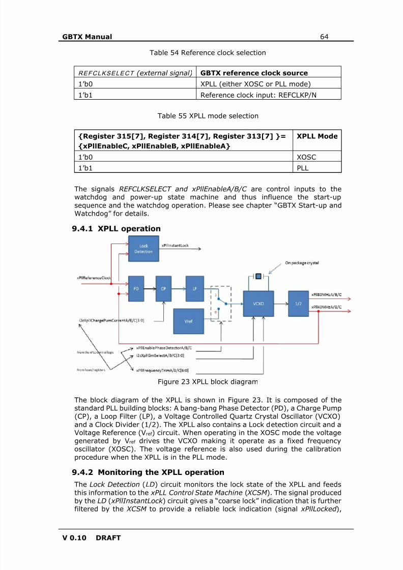
8/15/2019 gbtx Manual
http://slidepdf.com/reader/full/gbtx-manual 64/200
GBTX Manual 64
V 0.10 DRAFT
Table 54 Reference clock selection
REFCLKSELEC T (external signal) GBTX reference clock source
1’b0 XPLL (either XOSC or PLL mode)1’b1 Reference clock input: REFCLKP/N
Table 55 XPLL mode selection
Register 315[7], Register 314[7], Register 313[7] =xPllEnableC, xPllEnableB, xPllEnableA
XPLL Mode
1’b0 XOSC1’b1 PLL
The signals REFCLKSELECT and xPllEnableA/B/C are control inputs to the
watchdog and power-up state machine and thus influence the start-upsequence and the watchdog operation. Please see chapter “GBTX Start-up andWatchdog” for details.
9.4.1 XPLL operation
Figure 23 XPLL block diagram
The block diagram of the XPLL is shown in Figure 23. It is composed of thestandard PLL building blocks: A bang-bang Phase Detector (PD), a Charge Pump(CP), a Loop Filter (LP), a Voltage Controlled Quartz Crystal Oscillator (VCXO)and a Clock Divider (1/2). The XPLL also contains a Lock detection circuit and aVoltage Reference (V ref ) circuit. When operating in the XOSC mode the voltagegenerated by V ref drives the VCXO making it operate as a fixed frequencyoscillator (XOSC). The voltage reference is also used during the calibrationprocedure when the XPLL is in the PLL mode.
9.4.2 Monitoring the XPLL operation
The Lock Detection ( LD) circuit monitors the lock state of the XPLL and feedsthis information to the xPLL Control State Machine ( XCSM ). The signal producedby the LD ( xPllInstantLock ) circuit gives a “coarse lock” indication that is furtherfiltered by the XCSM to provide a reliable lock indication (signal xPllLocked ),
8/15/2019 gbtx Manual
http://slidepdf.com/reader/full/gbtx-manual 65/200
GBTX Manual 65
V 0.10 DRAFT
eliminating locking glitches (during the lock process) and possible glitches(during normal operation) due to single event upsets. The lock state of the XPLLcan be monitored by reading registers bits 4 and 7 of registers 427 and 428respectively:
• Register 428[7] = xPllInstantLock (“raw” xPLL lock indication)
•
Register 427[4] = xPllLocked (xPLL lock flag – processed by the XCSM )
9.4.2.1 Test Output
For testing purposes the signals xPllInstantLock and xPllLocked can be alsomonitored through the test output port “ TESTOUTPUT ” (see chapter 18 for pinnumber) according to Table 56) .
Table 56 Setting the TESTOUT port to monitor xPllInstantLock and xPllLocked
Register 280[7:0] = testOutputSelect[7:0] T E S T O U T P U T
8’d24 xPllInstantLock 8’d29 xPllLocked See section 16.3 for a complete list of signals available through theTESTOUTPUT port.
9.4.3 Setting the XPLL operation modes
As described above the xPLL can be bypassed, act as a crystal oscillator or asa PLL. How to set the different modes is described in the following sections.
9.4.3.1 Bypassing the XPLL
Bypassing the xPLL means that an external clock is directly used as thereference clock for the receiver and transmitter sections of the GBTX. Theexternal clock is also used as the master clock for the start-up and watchdoglogic. To bypass the xPLL, the GBTX must be setup as follows:
• Provide a 40.0786 MHz clock to the differential clock reference inputREFCLKP / REFCLKN. This input accepts LVS and SLVS levels and it isinternally terminated to 100 Ω (differential).
• Set the GBTX input REFCLKSELECT = 1’b1 (see Table 54) . This is a CMOSinput with 1’b1 = 1.5V
• Set clock manager register 281 as:o Register 281[1:0] = cmReferenceClockSelectB[1:0] = 2’b00o Register 281[3:2] = cmReferenceClockSelectB[1:0] = 2’b00o Register 281[5:4] = cmReferenceClockSelectC[1:0] = 2’b00
• Set the following xPLL registers as:o Register 235[3:0] = xPllChargePumpCurrentA[3:0] = 4’b0000o Register 235[7:4] = xPllChargePumpCurrentB[3:0] = 4’b0000o Register 236[3:0] = xPllChargePumpCurrentC[3:0] = 4’b0000o Register 313[6:0] = xPllFrequencyTrimA[6:0] = 7’bxxxxxxxo Register 313[7] = xPllEnableA = 1’b0o Register 314[6:0] = xPllFrequencyTrimB[6:0] = 7’bxxxxxxxo Register 314[7] = xPllEnableB = 1’b0o Register 315[6:0] = xPllFrequencyTrimC[6:0] = 7’bxxxxxxxo Register 315[7] = xPllEnableC = 1’b0
8/15/2019 gbtx Manual
http://slidepdf.com/reader/full/gbtx-manual 66/200
GBTX Manual 66
V 0.10 DRAFT
o Register 316[3:0] = xPllGmSelectA[3:0] = 4’b0000o Register 316[7:4] = xPllGmSelectB[3:0] = 4’b0000o Register 317[3:0] = xPllGmSelectC[3:0] = 4’b0000o Register 317[4] = xPllEnablePhaseDetectorA = 1’bxo Register 317[5] = xPllEnablePhaseDetectorB = 1’bxo Register 317[6] = xPllEnablePhaseDetectorC = 1’bxo Register 318[0] = xPllControlOverrideA = 1’b0o Register 318[1] = xPllControlOverrideB = 1’b0o Register 318[2] = xPllControlOverrideC = 1’b0o Register 318[3] = xPllEnableAutoRestartA = 1’bxo Register 318[4] = xPllEnableAutoRestartB = 1’bxo Register 318[5] = xPllEnableAutoRestartC = 1’bx
Please see 10.1 for details on the start-up sequence under these conditions.Note that in this mode the contents of registers 313[6:0], 314[6:0], 315[6:0],317[6:4] and 318[5:3] are ignored. Registers 235, 236[7:4], 316 and 317[3:0]although not influencing the behaviour of the chip in this mode should be setas indicated to reduce the power consumption.
9.4.3.2 Quartz Crystal Oscillator (XOSC) Mode
In the XOSC mode the GBTX generates the reference clock internally and anexternal reference clock is thus not required. The internal clock is used as areference for the receiver and transmitter and as the master clock for thewatchdog and start-up state machines. There are two methods of setting upthe XOSC mode. The first is slightly simpler to setup but doesn’t allow trimmingof the oscillator frequency (set to its lower oscillation frequency). The secondrequires a few more registers to be controlled but allows the user to trim theoscillator frequency.
9.4.3.2.1 Setting up the XOSC mode, method 1:
• Set the GBTX input REFCLKSELECT = 1’b0 (see Table 54) . This is a CMOSinput with 1’b0 = 0.0V
• Set the following registers as:o Register 235[3:0] = xPllChargePumpCurrentA[3:0] = 4’b0000o Register 235[7:4] = xPllChargePumpCurrentB[3:0] = 4’b0000o Register 236[3:0] = xPllChargePumpCurrentC[3:0] = 4’b0000o Register 313[6:0] = xPllFrequencyTrimA[6:0] = 7’b1011101
(default value)o Register 313[7] = xPllEnableA = 1’b0o Register 314[6:0] = xPllFrequencyTrimB[6:0] = 7’b1011101
(default value)o Register 314[7] = xPllEnableB = 1’b0o Register 315[6:0] = xPllFrequencyTrimC[6:0] = 7’b1011101
(default value)o Register 315[7] = xPllEnableC = 1’b0o Register 316[3:0] = xPllGmSelectA[3:0] = 4’b1010o Register 316[7:4] = xPllGmSelectB[3:0] = 4’b1010o Register 317[3:0] = xPllGmSelectC[3:0] = 4’b1010o Register 317[4] = xPllEnablePhaseDetectorA = 1’bxo Register 317[5] = xPllEnablePhaseDetectorB = 1’bxo Register 317[6] = xPllEnablePhaseDetectorC = 1’bx
8/15/2019 gbtx Manual
http://slidepdf.com/reader/full/gbtx-manual 67/200
8/15/2019 gbtx Manual
http://slidepdf.com/reader/full/gbtx-manual 68/200
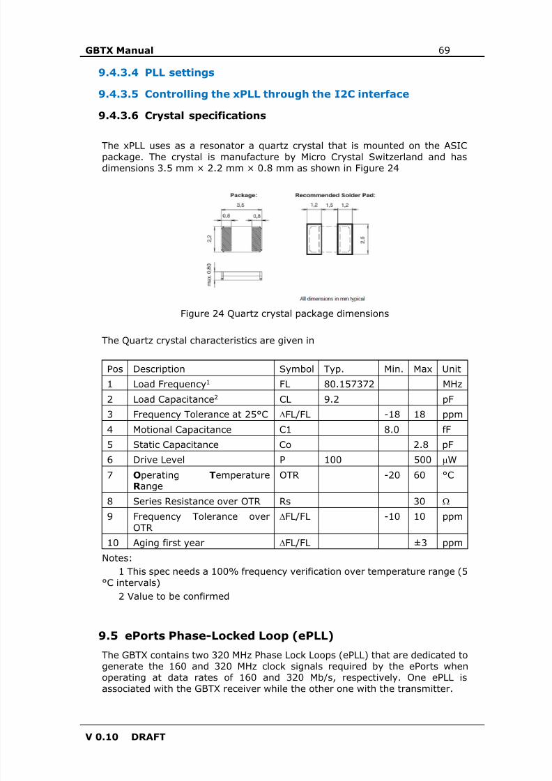
8/15/2019 gbtx Manual
http://slidepdf.com/reader/full/gbtx-manual 69/200
GBTX Manual 69
V 0.10 DRAFT
9.4.3.4 PLL settings
9.4.3.5 Controlling the xPLL through the I2C interface
9.4.3.6 Crystal specifications
The xPLL uses as a resonator a quartz crystal that is mounted on the ASICpackage. The crystal is manufacture by Micro Crystal Switzerland and hasdimensions 3.5 mm × 2.2 mm × 0.8 mm as shown in Figure 24
Figure 24 Quartz crystal package dimensions
The Quartz crystal characteristics are given in
Pos Description Symbol Typ. Min. Max Unit1 Load Frequency 1 FL 80.157372 MHz2 Load Capacitance 2 CL 9.2 pF
3 Frequency Tolerance at 25°C ∆FL/FL -18 18 ppm4 Motional Capacitance C1 8.0 fF5 Static Capacitance Co 2.8 pF6 Drive Level P 100 500 µW
7 O perating TemperatureR ange
OTR -20 60 °C
8 Series Resistance over OTR Rs 30 Ω
9 Frequency Tolerance overOTR
∆FL/FL -10 10 ppm
10 Aging first year ∆FL/FL ±3 ppmNotes:1 This spec needs a 100% frequency verification over temperature range (5
°C intervals)2 Value to be confirmed
9.5 ePorts Phase-Locked Loop (ePLL)
The GBTX contains two 320 MHz Phase Lock Loops (ePLL) that are dedicated togenerate the 160 and 320 MHz clock signals required by the ePorts whenoperating at data rates of 160 and 320 Mb/s, respectively. One ePLL isassociated with the GBTX receiver while the other one with the transmitter.
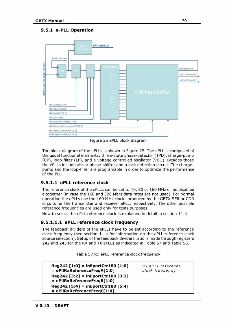
8/15/2019 gbtx Manual
http://slidepdf.com/reader/full/gbtx-manual 70/200
GBTX Manual 70
V 0.10 DRAFT
9.5.1 e-PLL Operation
Figure 25 ePLL block diagram
The block diagram of the ePLLs is shown in Figure 25. The ePLL is composed ofthe usual functional elements: three-state phase-detector (TPD), charge-pump(CP), loop-filter (LF), and a voltage controlled oscillator (VCO). Besides thosethe ePLLs include also a phase-shifter and a lock detection circuit. The charge-
pump and the loop-filter are programable in order to optimize the performanceof the PLL.
9.5.1.1 ePLL reference clock
The reference clock of the ePLLs can be set to 40, 80 or 160 MHz or be disabledaltogether (in case the 160 and 320 Mb/s data rates are not used). For normaloperation the ePLLs use the 160 MHz clocks produced by the GBTX SER or CDRcircuits for the transmitter and receiver ePLL, respectively. The other possiblereference frequencies are used only for tests purposes.How to select the ePLL reference clock is explained in detail in section 11.4
9.5.1.1.1 ePLL reference clock frequency
The feedback dividers of the ePLLs have to be set according to the referenceclock frequency (see section 11.4 for information on the ePLL reference clocksource selection). Setup of the feedback dividers ratio is made through registers242 and 243 for the RX and TX ePLLs as indicated in Table 57 and Table 58.
Table 57 Rx ePLL reference clock frequency
Reg242 [1:0] = inEportCtr180 [1:0]= ePllRxReferenceFreqA[1:0]Reg242 [3:2] = inEportCtr180 [3:2]= ePllRxReferenceFreqB[1:0]Reg242 [5:4] = inEportCtr180 [5:4]= ePllRxReferenceFreqC[1:0]
R x e P L L r e f e r e n c ec l o ck f r e q u e n c y
8/15/2019 gbtx Manual
http://slidepdf.com/reader/full/gbtx-manual 71/200
GBTX Manual 71
V 0.10 DRAFT
ePllRxReferenceFreq C/B/A[1:0] = 00 0
ePllRxReferenceFreq C/B/A[1:0] = 01 40 MHz
ePllRxReferenceFreq C/B/A[1:0] = 10 80 MHz
ePllRxReferenceFreq C/B/A[1:0] = 11 160 MHz
Table 58 Tx ePLL reference clock frequency
Reg243 [1:0] = inEportCtr181 [1:0]= ePllTxReferenceFreqA[1:0]Reg243 [3:2] = inEportCtr181 [3:2]= ePllTxReferenceFreqB[1:0]Reg243 [5:4] = inEportCtr181 [5:4]= ePllTxReferenceFreqC[1:0]
T x e P L L r e f e r e n c ec l o ck f r e q u e n c y
ePllTxReferenceFreq C/B/A[1:0] = 00 0
ePllTxReferenceFreq C/B/A[1:0] = 01 40 MHz
ePllTxReferenceFreq C/B/A[1:0] = 10 80 MHz
ePllTxReferenceFreq C/B/A[1:0] = 11 160 MHz
9.5.1 160 and 320 MHz internal clock phases
The 160 and 320 MHz (internal) clock phases are adjusted in the transmitterand receiver ePLLs. This is made to ensure the correctness of the internaltiming. The correct values for all internal clock phases will be pre-programed in the e-Fuse bank and the users are not allowed to modifythem at the risk of malfunctioning of the device.The phases of the 160 and 320 MHz clocks can be phase shifted up to 360
degrees in steps of 195.31 ps according to the phase control words given in thefour tables below. To obtain the phase of the clock signal in question multiplythe binary number written in the control register by 195.31 ps. Notice that foreach clock signal the triplicated numbers (A/B/C) must all be written with thesame value.
Table 59 Tx 320 MHz clock phase control registers
Register Name Signal
291 [3:0] ckCtr22 [3:0] ePllTxPhase320MHzA[3:0]291 [7:4] ckCtr22 [7:4] ePllTxPhase320MHzB[3:0]
292 [3:0] ckCtr23 [3:0] ePllTxPhase320MHzC[3:0]
Table 60 Tx 160 MHz clock phase control registers
Register Name Signal
296 [4:0] ckCtr27 [4:0] ePllTxPhase160MHzA[4:0]297 [4:0] ckCtr28 [4:0] ePllTxPhase160MHzB[4:0]298 [4:0] ckCtr29 [4:0] ePllTxPhase160MHzC[4:0]
8/15/2019 gbtx Manual
http://slidepdf.com/reader/full/gbtx-manual 72/200
GBTX Manual 72
V 0.10 DRAFT
Table 61 Rx 320 MHz clock phase control registers
Register Name Signal
302 [3:0] ckCtr33 [3:0] ePllRxPhase320MHzA[3:0]302 [7:4] ckCtr33 [7:4] ePllRxPhase320MHzB[3:0]292 [7:4] ckCtr23 [7:4] ePllRxPhase320MHzC[3:0]
Table 62 Rx 160 MHz clock phase control registers
Register Name Signal
307 [4:0] ckCtr38 [4:0] ePllRxPhase160MHzA[4:0]308 [4:0] ckCtr39 [4:0] ePllRxPhase160MHzB[4:0]309 [4:0] ckCtr40 [4:0] ePllRxPhase160MHzC[4:0]
9.5.1.1 Controlling the loop dynamics
The PLL dynamic behaviour can be programed by controlling the value of thecharge-pump
9.5.2 ePLL control state machine
This is a state-machine which monitors the status of the ePLL. There is oneblock for ePLL-RX and one for ePLL-TX. The locked status will be asserted onlywhen the ePLL stays locked for more than 800 consecutive cycles of thereference clock. The locked status will be de-asserted only when the ePLL stays
unlocked for more than 32 consecutive cycles of the reference clock.The state machine is automatically reset at power-up and by the external reset.It can also be reset by setting bits in a configuration register via I2C as shownin Table 63. These are the same resets used for the ePLLs themselves.
Table 63 ePLL reset control
Parameter Register Bits FunctionePllTxReset[C, B, A] 303 = ckCtr34 [2:0] Resets ePLL-TX controlePllRxReset[C, B, A] 303 = ckCtr34 [6:4] Resets ePLL-RX control
The block contains a loss-of-lock counter that can be read through I2c or SC-IC. It will increment when the state-machine de-asserts the locked status. Thiscounter is not resettable.
8/15/2019 gbtx Manual
http://slidepdf.com/reader/full/gbtx-manual 73/200
GBTX Manual 73
V 0.10 DRAFT
10. GBTX START-UP AND WATCHDOG
When the GBTX is powered or the external reset is asserted, the chip will runan automatic configuration sequence. This is controlled by a finite-statemachine (FSM), which issues resets to various blocks and monitors the state ofthe blocks until the complete chip is ready for operation. According to the choiceof mode, the FSM will ignore unused blocks. When the GBTX is ready foroperation, the FSM will assert the txRdy and rxRdy outputs.The FSM is synchronous with the reference clock of the GBTX, selected by theexternal signal REFCLKSELECT .When the user chooses to configure the GBTX from its fuse values (see Chapter15) , the sampling of the fuse values is controlled by the FSM.Watchdog monitoring can also be used in the GBTX. This will automatically reseta particular block if it malfunctions.To allow debugging, the automatic changing of states can be disabled and theFSM stepped through its various states under control of the I2C interface.
10.1 Recommendations for powering sequence of theGBTX
The start-up of the GBTX relies on the power being stable when the sequencestarts. This depends on the ramp-up time of the power supply, for example aDC-DC convertor or linear regulator. If the power is not stable when thesequence starts, this can cause incorrect sampling of the fuse values and hencethe wrong configuration of the chip. The following steps should be taken toprotect against this problem:
1. If a fail-safe mechanism of providing a reset to the GBTX is available, thisshould be used by connecting it to the RESETB input.
2. If the GBTX has no external clock and uses the XPLL to generate itsreference clock (XOSC mode, as described in Chapter 9.4 withREFCLKSELECT=0), then the FSM will pass through a 300 us wait-state. Insome cases, these 300 us will be sufficient for the power supply to stabilisebefore the fuse sampling starts. As an extra measure, the user shouldimplement the passive circuit described below.
3. In all scenarios, the user should implement a passive resistor-capacitornetwork connected to the RESETB input of the GBTX. The resistor should beconnected between RESETB and VDDIO, and the capacitor between RESETBand GND. The values of R and C depend on the ramp-up time of the supply.As an example, for the FEAST-MP DC-DC convertor typically used to powerthe GBTX, values of R = 5 k Ω and C = 100nF are found to be ideal.
4. If the FEAST-MP DC-DC convertor is used, the ‘power-good’ output of thisdevice can be used as a power-on-reset signal to the GBTX directlyconnected to its RESETB input. The ‘power-good’ output of the FEAST-MP isan open-drain configuration that requires a pull-up resistor to the outputvoltage of the convertor. This has been tested with one FEAST-MP poweringone GBTX, but has not been tested with multiple GBTXs powered from thesame FEAST-MP. The user should verify in their system that this ‘power-good’ signal does not introduce spurious glitches that would reset the GBTX.
8/15/2019 gbtx Manual
http://slidepdf.com/reader/full/gbtx-manual 74/200
GBTX Manual 74
V 0.10 DRAFT
The ‘power-good’ signal can be used together with a passive resistor-capacitor network as described above.
5. If the GBTX is operated with an external clock (REFCLKSELECT=1), the usershould enable this clock only after the power is switched on and has
stabilised.
6. The timeOut function should be enabled.
10.2 Power-up state FSM
The FSM is shown in Figure 26. The states are colour-coded according to thesub-blocks they control or monitor. The functions of each state are explained inTable 64.
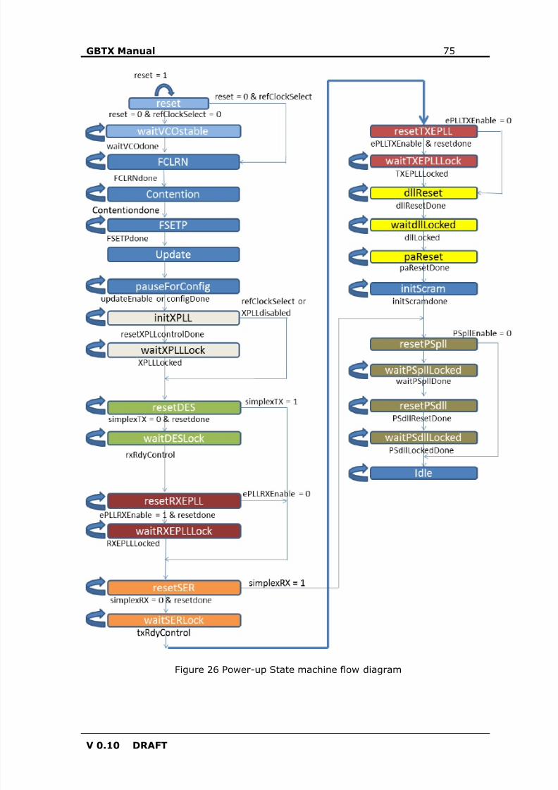
8/15/2019 gbtx Manual
http://slidepdf.com/reader/full/gbtx-manual 75/200
GBTX Manual 75
V 0.10 DRAFT
Figure 26 Power-up State machine flow diagram
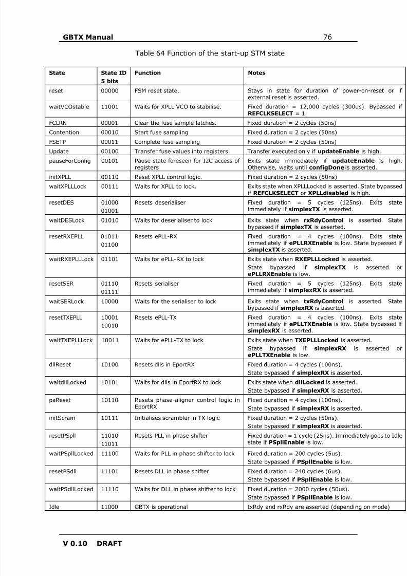
8/15/2019 gbtx Manual
http://slidepdf.com/reader/full/gbtx-manual 76/200
GBTX Manual 76
V 0.10 DRAFT
Table 64 Function of the start-up STM state
State State ID5 bits
Function Notes
reset 00000 FSM reset state. Stays in state for duration of power-on-reset or ifexternal reset is asserted.
waitVCOstable 11001 Waits for XPLL VCO to stabilise. Fixed duration = 12,000 cycles (300us). Bypassed ifREFCLKSELECT = 1.
FCLRN 00001 Clear the fuse sample latches. Fixed duration = 2 cycles (50ns)
Contention 00010 Start fuse sampling Fixed duration = 2 cycles (50ns)
FSETP 00011 Complete fuse sampling Fixed duration = 2 cycles (50ns)
Update 00100 Transfer fuse values into registers Transfer executed only if updateEnable is high.
pauseForConfig 00101 Pause state foreseen for I2C access ofregisters
Exits state immediately if updateEnable is high.Otherwise, waits until configDone is asserted.
initXPLL 00110 Reset XPLL control logic. Fixed duration = 2 cycles (50ns)
waitXPLLLock 00111 Waits for XPLL to lock. Exits state when XPLLLocked is asserted. State bypassedif REFCLKSELECT or XPLLdisabled is high.
resetDES 0100001001
Resets deserialiser Fixed duration = 5 cycles (125ns). Exits stateimmediately if simplexTX is asserted.
waitDESLock 01010 Waits for deserialiser to lock Exits state when rxRdyControl is asserted. Statebypassed if simplexTX is asserted.
resetRXEPLL 0101101100
Resets ePLL-RX Fixed duration = 4 cycles (100ns). Exits stateimmediately if ePLLRXEnable is low. State bypassed ifsimplexTX is asserted.
waitRXEPLLLock 01101 Waits for ePLL-RX to lock Exits state when RXEPLLLocked is asserted.State bypassed if simplexTX is asserted orePLLRXEnable is low.
resetSER 0111001111
Resets serialiser Fixed duration = 5 cycles (125ns). Exits stateimmediately if simplexRX is asserted.
waitSERLock 10000 Waits for the serialiser to lock Exits state when txRdyControl is asserted. Statebypassed if simplexRX is asserted.
resetTXEPLL 1000110010
Resets ePLL-TX Fixed duration = 4 cycles (100ns). Exits stateimmediately if ePLLTXEnable is low. State bypassed ifsimplexRX is asserted.
waitTXEPLLLock 10011 Waits for ePLL-TX to lock Exits state when TXEPLLLocked is asserted.State bypassed if simplexRX is asserted orePLLTXEnable is low.
dllReset 10100 Resets dlls in EportRX Fixed duration = 4 cycles (100ns).State bypassed if simplexRX is asserted.
waitdllLocked 10101 Waits for dlls in EportRX to lock Exits state when dllLocked is asserted.State bypassed if simplexRX is asserted.
paReset 10110 Resets phase-aligner control logic inEportRX
Fixed duration = 4 cycles (100ns).State bypassed if simplexRX is asserted.
initScram 10111 Initialises scrambler in TX logic Fixed duration = 2 cycles (50ns).State bypassed if simplexRX is asserted.
resetPSpll 1101011011
Resets PLL in phase shifter Fixed duration = 1 cycle (25ns). Immediately goes to Idlestate if PSpllEnable is low.
waitPSpllLocked 11100 Waits for PLL in phase shifter to lock Fixed duration = 200 cycles (5us).State bypassed if PSpllEnable is low.
resetPSdll 11101 Resets DLL in phase shifter Fixed duration = 240 cycles (6us).State bypassed if PSpllEnable is low.
waitPSdllLocked 11110 Waits for DLL in phase shifter to lock Fixed duration = 2000 cycles (50us).State bypassed if PSpllEnable is low.
Idle 11000 GBTX is operational txRdy and rxRdy are asserted (depending on mode)
8/15/2019 gbtx Manual
http://slidepdf.com/reader/full/gbtx-manual 77/200
GBTX Manual 77
V 0.10 DRAFT
Signal Userselectable?
Function and Source Register to address
REFCLKSELECT Yes Selects reference clock for GBTX (0=XPLL,1=external clock)
-
updateEnable Yes Enables automatic transfer of fuse values toregisters. updateEnable is high if the fuses
configFuse[2:0] have been burned (value =111).
Efuse 366; bits[2:0]
configDone Yes Signals that the user has finished an I2C accessand the FSM should continue. configDone isasserted by writing 8’hAA into the register.
Register 365; bits [7:0]
XPLLLocked No Indicates that the XPLL is locked. Generated bythe XPLL control block.
-
XPLLdisabled Yes Indicates that the XPLL is not used as a PLL andis running in VCO mode.Asserted if xpllEnable[C, B, A]=0.
Register 313; bit[7]Register 314; bit[7]Register 315; bit[7]
simplexTX Yes Indicates that the GBTX is in simplex transmittermode.Asserted if the external mode bits[1:0] = 00.
-
rxRdyControl No Indicates that the serialiser is operational.Generated by the RX control block.
-
ePLLRXEnable Yes Indicates that the ePLL-RX is in use. Asserted ifany of the phases of the ePLL-RX are enabled.
Register 304; bits[7:0]Register 305; bits[7:0]Register 306; bits[7:0]
RXEPLLLocked No Indicates that the ePLL-RX is operational.Generated by the ePLL-RX control block.
-
simplexRX Yes Indicates that the GBTX is in simplex receivermode.Asserted if the external mode bits[1:0] = 01.
-
txRdyControl No Indicates that the deserialiser is operational.Generated by the TX control block.
-
ePLLTXEnable Yes Indicates that the ePLL-TX is in use. Asserted ifany of the phases of the ePLL-RX are enabled.
Register 293; bits[7:0]Register 294; bits[7:0]Register 295; bits[7:0]
TXEPLLLocked No Indicates that the ePLL-TX is operational.Generated by the ePLL-TX control block.
-
dllLocked No Asserted if the dlls in all enabled EportRX groupsare locked
-
PSpllEnable Yes Indicates that the phase-shifter pll is in use.Asserted if PSpllEnable[C, B, A]=1
Register 52; bits[2:0]
10.3 Pausing the FSM
The pauseForConfig state is foreseen for initial testing of the GBTX when optimalregisters settings are not yet known and the Efuses have not been burned. IfupdateEnable is not asserted, the FSM will wait in this state until configDone isasserted. While in this state, the user can use the I2C interface to write valuesto the registers, and when this is finished the configDone bits should be set bywriting to the register described in Table 118. The FSM then will then continuethe rest of the sequence.Note that the configDone bits are reset to zero at power-on or when the externalreset is asserted.
8/15/2019 gbtx Manual
http://slidepdf.com/reader/full/gbtx-manual 78/200
GBTX Manual 78
V 0.10 DRAFT
10.4 Watchdog operation
When enabled, this will monitor the state of each sub-block. If any sub-blockstops operating correctly (for example a PLL loses lock), the watchdog will forcethe FSM to return to the reset state of that sub-block and the sequence willcontinue from that point until normal operating conditions are achieved.For example, if the FSM is in the Idle state and the ePLL-TX loses lock(TXEPLLLocked goes low), the FSM will jump back to the resetTXEPLL state andre-start the sequence from there.The intended use of the watchdog is to allow the chip to automatically recoverfrom a functional interruption (such as a fibre disconnect) without the need ofpower-cycling or resetting. It does however have an impact on the number ofdata errors caused by a single-event-upset, as discussed below.
The watchdog is enabled by asserting the following bits:Register 50 (wdogCtr0); bits[2:0] = 111.
10.5 AutoReset feature (GBTX version 2 only)The user can turn on the autoReset feature to ensure that the FSM is correctlyinitialised before executing the full start-up procedure.The autoReset feature is enabled by asserting the external signalautoReset/SLVS-Test-Inject.
10.6 TimeOut feature (GBTX version 2 only)
Some of the states of the FSM wait for a particular circuit to lock. In some cases,this locking may not occur (for example, if the downlink optical fibre isunplugged when the GBTX is powered-on then the deserialiser will not lock). To
resolve problems like this, the ‘wait-states’ have time-outs (set at 2 seconds).If this time is exceeded the FSM moves back to the reset state and re-startsthe full start-up procedure. In the example, the FSM will continue this time-outloop until the fibre is plugged in and the deserialiser can lock.The timeOut is applied to the following states:waitXPLLLock, waitDESLock, waitRXEPLLLock, waitSERLock, waitTXEPLLLock,waitdllLocked.
The timeOut is enabled by asserting the following bits:Register 52 (wdogCtr2); bits[5:3] = 111.
When the GBTX is already operating (FSM is in the idle state) and a problemoccurs that lasts a long time (for example, the downlink fibre is unplugged) thecombination of the watchdog and timeOut features will ensure that the GBTXautomatically recovers when the problem is resolved (the reconnection of thefibre).
10.7 Notes on using the watchdog in an SEU environment
The GBTX has been extensively tested with heavy ions provoking single-eventupsets in the chip. In particular, the sensitivity of the serialiser/deserialisercircuits to SEUs and the resulting data errors have been measured (see [19] formore details). With the watchdog disabled, it has been observed that the chip
always recovers to its functional state after an SEU. A certain number of bit andframe errors occur while the chip is recovering. With the watchdog enabled, the
8/15/2019 gbtx Manual
http://slidepdf.com/reader/full/gbtx-manual 79/200
GBTX Manual 79
V 0.10 DRAFT
chip again recovers back to its functional state but the recovery process islonger and hence more bit and frame errors are observed.The user should therefore carefully assess the advantages and disadvantagesof enabling the watchdog if they will operate in a significant radiationenvironment.
10.8 Disabling the power-up sequence
The FSM can be halted at any time by asserting the stateOverride externalsignal. The state is then selected by the value written to a configurationregister:Register 51 (wdogCtr1); bits[4:0].The 5-bit state identifiers are listed in Table 64.
10.9 Summary of Configuration inputs
The registers listed in Table 65 are used to configure the power-up state
machine. Table 65 Power-up configuration registers
Register address Register name Bits
Efuse 366 bits[2:0]Register 365 configDone bits [7:0]Register 313 ckCtr44 bit[7]Register 314 ckCtr45 bit[7]Register 315 ckCtr46 bit[7]Register 304 ckCtr35 bits[7:0]Register 305 ckCtr36 bits[7:0]Register 306 ckCtr37 bits[7:0]Register 293 ckCtr24 bits[7:0]Register 294 ckCtr25 bits[7:0]Register 295 ckCtr26 bits[7:0]Register 52 wdogCtr2 bits[2:0]Register 50 wdogCtr0 bits[2:0]Register 51 wdogCtr1 bits[4:0]
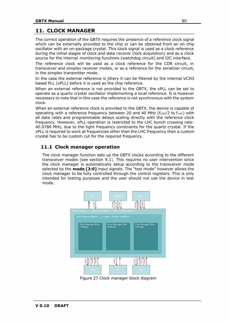
8/15/2019 gbtx Manual
http://slidepdf.com/reader/full/gbtx-manual 80/200
GBTX Manual 80
V 0.10 DRAFT
11. CLOCK MANAGER
The correct operation of the GBTX requires the presence of a reference clock signalwhich can be externally provided to the chip or can be obtained from an on chiposcillator with an on-package crystal. This clock signal is used as a clock referenceduring the initial stages of clock and data recover (lock acquisition) and as a clocksource for the internal monitoring functions (watchdog circuit) and I2C interface.The reference clock will be used as a clock reference for the CDR circuit, intransceiver and simplex receiver modes, or as a reference for the serializer circuit,in the simplex transmitter mode.In the case the external reference is jittery it can be filtered by the internal VCXObased PLL (xPLL) before it is used as the chip reference.When an external reference is not provided to the GBTX, the xPLL can be set tooperate as a quartz crystal oscillator implementing a local reference. It is howevernecessary to note that in this case the reference is not synchronous with the systemclock.When an external reference clock is provided to the GBTX, the device is capable of
operating with a reference frequency between 20 and 40 MHz (f LHC /2 to f LHC) withall data rates and programmable delays scaling directly with the reference clockfrequency. However, xPLL operation is restricted to the LHC bunch crossing rate:40.0786 MHz, due to the tight frequency constraints for the quartz crystal. If thexPLL is required to work at frequencies other than the LHC frequency then a customcrystal has to be custom cut for the required frequency.
11.1 Clock manager operation
The clock manager function sets up the GBTX clocks according to the differenttransceiver modes (see section 9.1) . This requires no user intervention sincethe clock manager is automatically setup according to the transceiver mode
selected by the mode [3:0] input signals. The “test mode” however allows theclock manager to be fully controlled through the control registers. This is onlyintended for testing purposes and the user should not use the device in testmode.
Figure 27 Clock manager block diagram
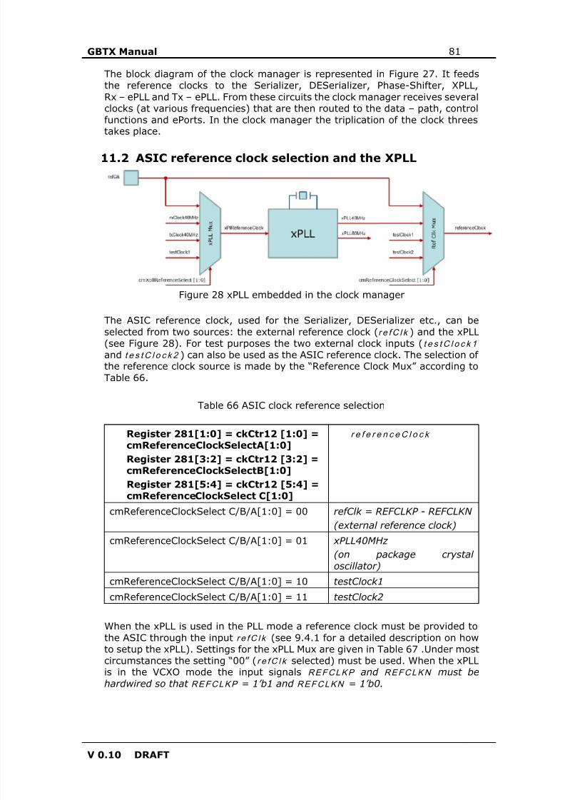
8/15/2019 gbtx Manual
http://slidepdf.com/reader/full/gbtx-manual 81/200
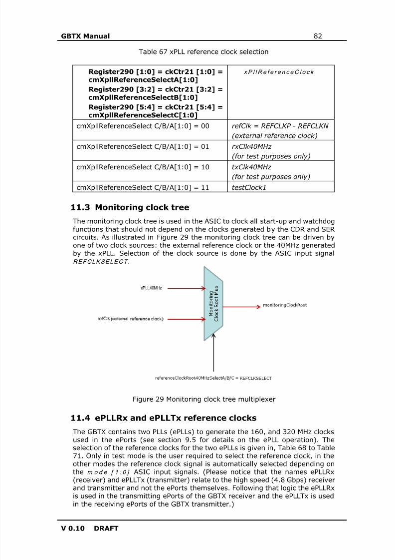
8/15/2019 gbtx Manual
http://slidepdf.com/reader/full/gbtx-manual 82/200
GBTX Manual 82
V 0.10 DRAFT
Table 67 xPLL reference clock selection
Register290 [1:0] = ckCtr21 [1:0] =cmXpllReferenceSelectA[1:0]Register290 [3:2] = ckCtr21 [3:2] =
cmXpllReferenceSelectB[1:0]Register290 [5:4] = ckCtr21 [5:4] =cmXpllReferenceSelectC[1:0]
x P l l R e f e r e n c e C l o c k
cmXpllReferenceSelect C/B/A[1:0] = 00 refClk = REFCLKP - REFCLKN(external reference clock)
cmXpllReferenceSelect C/B/A[1:0] = 01 rxClk40MHz(for test purposes only)
cmXpllReferenceSelect C/B/A[1:0] = 10 txClk40MHz(for test purposes only)
cmXpllReferenceSelect C/B/A[1:0] = 11 testClock1
11.3 Monitoring clock tree
The monitoring clock tree is used in the ASIC to clock all start-up and watchdogfunctions that should not depend on the clocks generated by the CDR and SERcircuits. As illustrated in Figure 29 the monitoring clock tree can be driven byone of two clock sources: the external reference clock or the 40MHz generatedby the xPLL. Selection of the clock source is done by the ASIC input signalREFCLK S ELECT.
Figure 29 Monitoring clock tree multiplexer
11.4 ePLLRx and ePLLTx reference clocks
The GBTX contains two PLLs (ePLLs) to generate the 160, and 320 MHz clocksused in the ePorts (see section 9.5 for details on the ePLL operation). Theselection of the reference clocks for the two ePLLs is given in, Table 68 to Table71. Only in test mode is the user required to select the reference clock, in theother modes the reference clock signal is automatically selected depending onthe m o d e [ 1 : 0 ] ASIC input signals. (Please notice that the names ePLLRx(receiver) and ePLLTx (transmitter) relate to the high speed (4.8 Gbps) receiver
and transmitter and not the ePorts themselves. Following that logic the ePLLRxis used in the transmitting ePorts of the GBTX receiver and the ePLLTx is usedin the receiving ePorts of the GBTX transmitter.)
8/15/2019 gbtx Manual
http://slidepdf.com/reader/full/gbtx-manual 83/200
GBTX Manual 83
V 0.10 DRAFT
Table 68 Receiver ePLL (ePLLRx) reference clock multiplexer
Mode [1:0] e P l l R x M u x ( r e f e r e n c ec lo c k m u l t i p l ex e r )
00 (simplex Tx) 001 (simplex Rx) rxClk160MHz10 (transceiver) rxClk160MHz
11 (test mode) ePllRxTestMux
Table 69 Receiver ePLL (ePLLRx) reference clock test multiplexer
Register0 [1:0] = ckCtr0 [1:0] =cmEpllRxReferenceSelectA[1:0]Register0 [3:2] = ckCtr0 [3:2] =cmEpllRxReferenceSelectB[1:0]Register0 [5:4] = ckCtr0 [5:4] =cmEpllRxReferenceSelectC[1:0]
e P l l R x T e s t M u x( r e f e r e n c e c lo c k t e s tm u l t i p l ex e r )
cmEpllRxReferenceSelect C/B/A[1:0] = 00 rxClk40MHzcmEpllRxReferenceSelect C/B/A[1:0] = 01 rxClk80MHzcmEpllRxReferenceSelect C/B/A[1:0] = 10 rxClk160MHz
cmEpllRxReferenceSelect C/B/A[1:0] = 11 testClock1
Table 70 Transmitter ePLL (ePLLRx) reference clock multiplexer
Mode [1:0] e P l l T x M u x ( r e f e r e n c ec lo c k m u l t i p l ex e r )
00 (simplex Tx) txClk160MHz01 (simplex Rx) 010 (transceiver) txClk160MHz
11 (test mode) ePllTxTestMux
Table 71 Transmitter ePLL (ePLLTx) reference clock test multiplexer
Register1 [1:0] = ckCtr1 [1:0] =cmEpllTxReferenceSelectA[1:0]Register1 [3:2] = ckCtr1 [3:2] =cmEpllTxReferenceSelectB[1:0]Register1 [5:4] = ckCtr1 [5:4] =cmEpllTxReferenceSelectC[1:0]
e P l l T x T e s t M u x( r e f e r e n c e c lo c k t e s tm u l t i p l ex e r )
cmEpllTxReferenceSelect C/B/A[1:0] = 00 txClk40MHzcmEpllTxReferenceSelect C/B/A[1:0] = 01 txClk80MHzcmEpllTxReferenceSelect C/B/A[1:0] = 10 txClk160MHz
cmEpllTxReferenceSelect C/B/A[1:0] = 11 testClock2
8/15/2019 gbtx Manual
http://slidepdf.com/reader/full/gbtx-manual 84/200
GBTX Manual 84
V 0.10 DRAFT
11.4.1 Selecting the reference clock frequency
The feedback dividers of the ePLLs must be programed so that the division ratiois set according to the reference frequency, for details section 9.5.1.1.1
11.5 Phase-Shifter reference clock
The phase-shifter reference clock is selected according to Table 72 and Table 73. The mode [1:0] ASIC input signals determine which clock is given as a referenceclock to the phase-shifter (see Table 72) . When in test mode the phase-shifter testmux has to be further setup (see Table 61) to select the phase-shifter referenceclock.
Table 72 Phase-Shifter reference clock multiplexer
Mode [1:0] p s M u x ( r e f e r en c e c lo c km u l t i p l ex e r )
00 (simplex Tx) txClk40MHz
01 (simplex Rx) rxClk40MHz10 (transceiver) rxClk40MHz
11 (test mode) psTestMux
Table 73 Phase-Shifter reference clock test multiplexer
Register282 [1:0] = ckCtr13 [1:0] =cmPsReferenceSelectA[1:0]Register282 [3:2] = ckCtr13 [3:2] =cmPsReferenceSelectB[1:0]
Register282 [5:4] = ckCtr13 [5:4] =cmPsReferenceSelectC[1:0]
p s Te s t M u x ( r e f e r e n c ec lo c k t e s t m u l t i p l ex e r )
cmPsReferenceSelect C/B/A[1:0] = 00 referenceClock(external or xPLL)
cmPsReferenceSelect C/B/A[1:0] = 01 txClk40MHz
cmPsReferenceSelect C/B/A[1:0] = 10 rxClk40MHz
cmPsReferenceSelect C/B/A[1:0] = 11 testClock1
11.6 Rx (CDR) reference clock
The high speed receiver (CDR) reference clock is automatically set by themode [1:0] ASIC input signals. However, when in test mode the user has thefreedom to choose the receiver reference clock source by setting the testmultiplexer. This is detailed in Table 74 and Table 75.
Table 74 Rx (CDR) reference clock multiplexer
Mode [1:0] r x R e f e r e n c e C l o c k( r e f e r e n c e cl o c km u l t i p l ex e r )
00 (simplex Tx) 0
01 (simplex Rx) referenceClock
8/15/2019 gbtx Manual
http://slidepdf.com/reader/full/gbtx-manual 85/200
GBTX Manual 85
V 0.10 DRAFT
10 (transceiver) referenceClock
11 (test mode) rxReferenceTestMux
Table 75 Rx (CDR) reference clock test multiplexer
Register2 [1:0] = ckCtr2 [1:0] =cmRxReferenceTestMuxSelectA[1:0]Register2 [3:2] = ckCtr2 [3:2] =cmRxReferenceTestMuxSelectB[1:0]Register2 [5:4] = ckCtr2 [5:4] =cmRxReferenceTestMuxSelectC[1:0]
r x R e f e r e n c e T e s t M u x( r e f e r e n c e cl o c kt e s t m u l t i p l ex e r )
cmRxReferenceTestMuxSelect C/B/A[1:0] = 00 referenceClock
cmRxReferenceTestMuxSelect C/B/A[1:0] = 01 txClk40MHz
cmRxReferenceTestMuxSelect C/B/A[1:0] = 10 testClock1
cmRxReferenceTestMuxSelect C/B/A[1:0] = 11 testClock2
11.1 Tx (SER) reference clock
The high speed transmitter (SER) reference clock is automatically set by themode [1:0] ASIC input signals. However, when in test mode the user has thefreedom to choose the transmitter reference clock source by setting the testmultiplexer. This is detailed in Table 76 and Table 77.
Table 76 Tx (SER) reference clock multiplexer
Mode [1:0] t x R e f e r e n c e C l o c k( r e f e r e n c e cl o c km u l t i p l ex e r )
00 (simplex Tx) referenceClock
01 (simplex Rx) 0
10 (transceiver) rxClk40MHz
11 (test mode) txReferenceTestMux
Table 77 Tx (SER) reference clock test multiplexer
Register3 [1:0] = ckCtr3 [1:0] =cmTxReferenceTestMuxSelectA[1:0]Register3 [3:2] = ckCtr3 [3:2] =cmTxReferenceTestMuxSelectB[1:0]Register3 [5:4] = ckCtr3 [5:4] =cmTxReferenceTestMuxSelectC[1:0]
t x R e f e r e n c e T e s t M u x( r e f e r e n c e c l o c k t e s tm u l t i p l ex e r )
cmTxReferenceTestMuxSelect C/B/A[1:0] =00
referenceClock
cmTxReferenceTestMuxSelect C/B/A[1:0] =01
rxClk40MHz
cmTxReferenceTestMuxSelect C/B/A[1:0] =
10
xPLL40MHz
8/15/2019 gbtx Manual
http://slidepdf.com/reader/full/gbtx-manual 86/200
GBTX Manual 86
V 0.10 DRAFT
cmTxReferenceTestMuxSelect C/B/A[1:0] =11
testClock1
11.2 Receiver (Rx) clocks
The GBTX receiver clocks are setup according to what is given in Table 78 toTable 85. All the receiver clocks are set automatically according to themode [1:0] ASIC input signals. Only the test mode allows the user choose theclock settings.
Table 78 Rx 40 MHz clock mux
Mode [1:0] r x M u x 4 0 M H z
00 (simplex Tx) 0
01 (simplex Rx) rxClk40MHz
10 (transceiver) rxClk40MHz
11 (test mode) rxTestMux40MHz
Table 79 Rx 40 MHz test clock mux
Register279 [1:0] = ckCtr10 [1:0] =cmRxTestMuxSelect40C[1:0]Register278 [1:0] = ckCtr9 [1:0] =cmRxTestMuxSelect40B[1:0]Register277 [1:0] = ckCtr8 [1:0] =cmRxTestMuxSelect40A[1:0]
r x T e s t M u x 4 0 M H z
cmRxTestMuxSelect40 C/B/A[1:0] = 00 rxClk40MHz
cmRxTestMuxSelect40 C/B/A[1:0] = 01 txClk40MHz
cmRxTestMuxSelect40 C/B/A[1:0] = 10 testClock1
cmRxTestMuxSelect40 C/B/A[1:0] = 11 testClock2
Table 80 Rx 80 MHz clock mux
Mode [1:0] r x M u x 8 0 M H z
00 (simplex Tx) 0
01 (simplex Rx) rxClk80MHz
10 (transceiver) rxClk80MHz
11 (test mode) rxTestMux80MHz
Table 81 Rx 80 MHz test clock mux
Register279 [3:2] = ckCtr10 [3:2] =
cmRxTestMuxSelect80C[1:0]
r x T e s t M u x 8 0 M H z
8/15/2019 gbtx Manual
http://slidepdf.com/reader/full/gbtx-manual 87/200
GBTX Manual 87
V 0.10 DRAFT
Register278 [3:2] = ckCtr9 [3:2] =cmRxTestMuxSelect80B[1:0]Register277 [3:2] = ckCtr8 [3:2] =cmRxTestMuxSelect80A[1:0]
cmRxTestMuxSelect80 C/B/A[1:0] = 00 rxClk80MHz
cmRxTestMuxSelect80 C/B/A[1:0] = 01 txClk80MHzcmRxTestMuxSelect80 C/B/A[1:0] = 10 testClock1
cmRxTestMuxSelect80 C/B/A[1:0] = 11 testClock2
Table 82 Rx 160 MHz clock mux
Mode [1:0] r x M u x 1 6 0 M H z
00 (simplex Tx) 0
01 (simplex Rx) ePllRx160MHx
10 (transceiver) ePllRx160MHz
11 (test mode) rxTestMux160MHz
Table 83 Rx 160 MHz test clock mux
Register279 [5:4] = ckCtr10 [5:4] =cmRxTestMuxSelect160C[1:0]Register278 [5:4] = ckCtr9 [5:4] =cmRxTestMuxSelect160B[1:0]Register277 [5:4] = ckCtr8 [5:4] =cmRxTestMuxSelect160A[1:0]
r x T e s t M u x 1 6 0 M H z
cmRxTestMuxSelect160 C/B/A[1:0] = 00 ePllRx160MHz
cmRxTestMuxSelect160 C/B/A[1:0] = 01 ePllTx160MHz
cmRxTestMuxSelect160 C/B/A[1:0] = 10 rxClk160MHz
cmRxTestMuxSelect160 C/B/A[1:0] = 11 testClock2
Table 84 Rx 320 MHz clock mux
Mode [1:0] r x M u x 3 2 0 M H z00 (simplex Tx) 0
01 (simplex Rx) ePllRx320MHz
10 (transceiver) ePllRx320MHz
11 (test mode) rxTestMux320MHz
Table 85 Rx 320 MHz test clock mux
Register279 [7:6] = ckCtr10 [7:6] =cmRxTestMuxSelect320C[1:0]
Register278 [7:6] = ckCtr9 [7:6] =cmRxTestMuxSelect320B[1:0]
r x T e s t M u x 3 2 0 M H z
8/15/2019 gbtx Manual
http://slidepdf.com/reader/full/gbtx-manual 88/200
GBTX Manual 88
V 0.10 DRAFT
Register277 [7:6] = ckCtr8 [7:6] =cmRxTestMuxSelect320A[1:0]
cmRxTestMuxSelect320 C/B/A[1:0] = 00 ePllRx320MHz
cmRxTestMuxSelect320 C/B/A[1:0] = 01 ePllTx320MHz
cmRxTestMuxSelect320 C/B/A[1:0] = 10 testClock1
cmRxTestMuxSelect320 C/B/A[1:0] = 11 testClock2
11.3 Transmitter (Tx) clocks
The GBTX transmitter clocks are setup according to what is given in Table 86to Table 93. All the transmitter clocks are set automatically according to themode [1:0] ASIC input signals. Only the test mode allows the user choose theclock settings.
Table 86 Tx 40 MHz clock mux
Mode [1:0] t x M u x 4 0 M H z
00 (simplex Tx) txClk40MHz
01 (simplex Rx) 0
10 (transceiver) txClk40MHz
11 (test mode) txTestMux40MHz
Table 87 Tx 40 MHz test clock mux
Register289 [1:0] = ckCtr20 [1:0] =cmTxTestMuxSelect40C[1:0]Register288 [1:0] = ckCtr19 [1:0] =cmTxTestMuxSelect40B[1:0]Register287 [1:0] = ckCtr18 [1:0] =cmTxTestMuxSelect40A[1:0]
t x T e s t M u x 4 0 M H z
cmTxTestMuxSelect40 C/B/A[1:0] = 00 rxClk40MHz
cmTxTestMuxSelect40 C/B/A[1:0] = 01 txClk40MHz
cmTxTestMuxSelect40 C/B/A[1:0] = 10 testClock1
cmTxTestMuxSelect40 C/B/A[1:0] = 11 testClock2
Table 88 Tx 80 MHz clock mux
Mode [1:0] t x M u x 8 0 M H z
00 (simplex Tx) txClk80MHz
01 (simplex Rx) 0
10 (transceiver) txClk80MHz
11 (test mode) txTestMux80MHz
8/15/2019 gbtx Manual
http://slidepdf.com/reader/full/gbtx-manual 89/200
GBTX Manual 89
V 0.10 DRAFT
Table 89 Tx 80 MHz test clock mux
Register289 [3:2] = ckCtr20 [3:2] =
cmTxTestMuxSelect80C[1:0]Register288 [3:2] = ckCtr19 [3:2] =cmTxTestMuxSelect80B[1:0]Register287 [3:2] = ckCtr18 [3:2] =cmTxTestMuxSelect80A[1:0]
t x T e s t M u x 8 0 M H z
cmTxTestMuxSelect80 C/B/A[1:0] = 00 rxClk80MHz
cmTxTestMuxSelect80 C/B/A[1:0] = 01 txClk80MHz
cmTxTestMuxSelect80 C/B/A[1:0] = 10 testClock1
cmTxTestMuxSelect80 C/B/A[1:0] = 11 testClock2
Table 90 Tx 160 MHz clock mux
Mode [1:0] t x M u x 1 6 0 M H z
00 (simplex Tx) ePllTx160MHz
01 (simplex Rx) 0
10 (transceiver) ePllTx160MHz
11 (test mode) txTestMux160MHz
Table 91 Tx 160 MHz test clock mux
Register289 [5:4] = ckCtr20 [5:4] =cmTxTestMuxSelect160C[1:0]Register288 [5:4] = ckCtr19 [5:4] =cmTxTestMuxSelect160B[1:0]Register287 [5:4] = ckCtr18 [5:4] =cmTxTestMuxSelect160A[1:0]
t x T e s t M u x 1 6 0 M H z
cmTxTestMuxSelect160 C/B/A[1:0] = 00 ePllRx160MHz
cmTxTestMuxSelect160 C/B/A[1:0] = 01 ePllTx160MHz
cmTxTestMuxSelect160 C/B/A[1:0] = 10 txClk160MHz
cmTxTestMuxSelect160 C/B/A[1:0] = 11 testClock1
Table 92 Tx 320 MHz clock mux
Mode [1:0] t x M u x 3 2 0 M H z
00 (simplex Tx) ePllTx320MHz
01 (simplex Rx) 0
10 (transceiver) ePllTx320MHz
11 (test mode) txTestMux320MHz
8/15/2019 gbtx Manual
http://slidepdf.com/reader/full/gbtx-manual 90/200
8/15/2019 gbtx Manual
http://slidepdf.com/reader/full/gbtx-manual 91/200
8/15/2019 gbtx Manual
http://slidepdf.com/reader/full/gbtx-manual 92/200
GBTX Manual 92
V 0.10 DRAFT
steps). It is possible to use the device by fixing the phase of the sampled clocksand sweep the phase of the sampling clock. However in this case the resolution willbe limited to the phase resolution of the sampling clock (±150 ps) in all cases.The sampled values can be observed through the testClockOut . Please see section16.4.2 for details on how to use and program the testClockOut signal.
Table 98 Clock root sampler output multiplexer
Register319[4:0]
Sampling clock Sampled clock Sample signal
0 n. a. n. a. n.a.
1 rxClockRoot40MHzA rxClockRoot80MHzA sampleRx4080A
2 rxClockRoot40MHzA rxClockRoot160MHzA sampleRx40160A
3 rxClockRoot40MHzA rxClockRoot320MHzA sampleRx40320A
4 rxClockRoot40MHzA rxClockRoot40MHzB sampleRx4040AB
5 rxClockRoot40MHzA rxClockRoot40MHzC sampleRx4040AC6 rxClockRoot40MHzB rxClockRoot80MHzB sampleRx4080B
7 rxClockRoot40MHzB rxClockRoot160MHzB sampleRx40160B
8 rxClockRoot40MHzB rxClockRoot320MHzB sampleRx40320B
9 rxClockRoot40MHzB rxClockRoot40MHzA sampleRx4040BA
10 rxClockRoot40MHzB rxClockRoot40MHzC sampleRx4040BC
11 rxClockRoot40MHzC rxClockRoot80MHzC sampleRx4080C
12 rxClockRoot40MHzC rxClockRoot160MHzC sampleRx40160C
13 rxClockRoot40MHzC rxClockRoot320MHzC sampleRx40320C
14 rxClockRoot40MHzC rxClockRoot40MHzA sampleRx4040CA15 rxClockRoot40MHzC rxClockRoot40MHzB sampleRx4040CB
16 txClockRoot40MHzA txClockRoot80MHzA sampleTx4080A
17 txClockRoot40MHzA txClockRoot160MHzA sampleTx40160A
18 txClockRoot40MHzA txClockRoot320MHzA sampleTx40320A
19 txClockRoot40MHzA txClockRoot40MHzB sampleTx4040AB
20 txClockRoot40MHzA txClockRoot40MHzC sampleTx4040AC
21 txClockRoot40MHzB txClockRoot80MHzB sampleTx4080B
22 txClockRoot40MHzB txClockRoot160MHzB sampleTx40160B
23 txClockRoot40MHzB txClockRoot320MHzB sampleTx40320B24 txClockRoot40MHzB txClockRoot40MHzA sampleTx4040BA
25 txClockRoot40MHzB txClockRoot40MHzC sampleTx4040BC
26 txClockRoot40MHzC txClockRoot80MHzC sampleTx4080C
27 txClockRoot40MHzC txClockRoot160MHzC sampleTx40160C
28 txClockRoot40MHzC txClockRoot320MHzC sampleTx40320C
29 txClockRoot40MHzC txClockRoot40MHzA sampleTx4040CA
30 txClockRoot40MHzC txClockRoot40MHzB sampleTx4040CB
31 n. a. n. a. 0

8/15/2019 gbtx Manual
http://slidepdf.com/reader/full/gbtx-manual 93/200
GBTX Manual 93
V 0.10 DRAFT
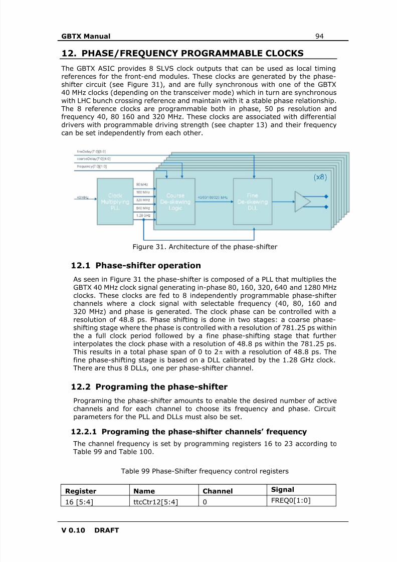
8/15/2019 gbtx Manual
http://slidepdf.com/reader/full/gbtx-manual 94/200
GBTX Manual 94
V 0.10 DRAFT
12. PHASE/FREQUENCY PROGRAMMABLE CLOCKS
The GBTX ASIC provides 8 SLVS clock outputs that can be used as local timingreferences for the front-end modules. These clocks are generated by the phase-shifter circuit (see Figure 31) , and are fully synchronous with one of the GBTX40 MHz clocks (depending on the transceiver mode) which in turn are synchronouswith LHC bunch crossing reference and maintain with it a stable phase relationship.The 8 reference clocks are programmable both in phase, 50 ps resolution andfrequency 40, 80 160 and 320 MHz. These clocks are associated with differentialdrivers with programmable driving strength (see chapter 13) and their frequencycan be set independently from each other.
Figure 31. Architecture of the phase-shifter
12.1 Phase-shifter operation
As seen in Figure 31 the phase-shifter is composed of a PLL that multiplies theGBTX 40 MHz clock signal generating in-phase 80, 160, 320, 640 and 1280 MHz
clocks. These clocks are fed to 8 independently programmable phase-shifterchannels where a clock signal with selectable frequency (40, 80, 160 and320 MHz) and phase is generated. The clock phase can be controlled with aresolution of 48.8 ps. Phase shifting is done in two stages: a coarse phase-shifting stage where the phase is controlled with a resolution of 781.25 ps withinthe a full clock period followed by a fine phase-shifting stage that furtherinterpolates the clock phase with a resolution of 48.8 ps within the 781.25 ps.This results in a total phase span of 0 to 2 π with a resolution of 48.8 ps. Thefine phase-shifting stage is based on a DLL calibrated by the 1.28 GHz clock.There are thus 8 DLLs, one per phase-shifter channel.
12.2 Programing the phase-shifter
Programing the phase-shifter amounts to enable the desired number of activechannels and for each channel to choose its frequency and phase. Circuitparameters for the PLL and DLLs must also be set.
12.2.1 Programing the phase-shifter channels’ frequency
The channel frequency is set by programming registers 16 to 23 according toTable 99 and Table 100.
Table 99 Phase-Shifter frequency control registers
Register Name Channel Signal16 [5:4] ttcCtr12[5:4] 0 FREQ0[1:0]
8/15/2019 gbtx Manual
http://slidepdf.com/reader/full/gbtx-manual 95/200
GBTX Manual 95
V 0.10 DRAFT
17 [5:4] ttcCtr13[5:4] 1 FREQ1[1:0]
18 [5:4] ttcCtr14[5:4] 2 FREQ2[1:0]
19 [5:4] ttcCtr15[5:4] 3 FREQ3[1:0]
20 [5:4] ttcCtr16[5:4] 4 FREQ4[1:0]
21 [5:4] ttcCtr17[5:4] 5 FREQ5[1:0]22 [5:4] ttcCtr18[5:4] 6 FREQ6[1:0]
23 [5:4] ttcCtr19[5:4] 7 FREQ7[1:0]
Table 100 Phase-Shifter frequency control settings
FREQX[1:0] with X = 0, 1, 2, 3, 4, 5, 6 & 7 Frequency in MHz
00 4001 8010 16011 320
12.2.2 Programming the phase-shifter channels’ phase
Programing a phase-shifter channel delay involves setting two parameters: thecoarse delay parameters CDLX[4:0] (with X = 0, 1, 2, 3, 4, 5, 6 & 7) and thefine delay parameters FDLX[3:0] (with X = 0, 1, 2, 3, 4, 5, 6 & 7). The channelphase-shift (or delay) is given by:
Channel Delay = CDLX[4:0] × 781.25 ps+ FDLX[3:0] × 48.8 ps
A list of the coarse and fine delay registers can be found in tables Table 101and Table 102 respectively.
Table 101 Coarse delay registers
Register Name Channel Signal
8 [4:0] ttcCtr4[4:0] 0 CDL0[4:0]
9 [4:0] ttcCtr5[4:0] 1 CDL1[4:0]
10 [4:0] ttcCtr6[4:0] 2 CDL2[4:0]
11 [4:0] ttcCtr7[4:0] 3 CDL3[4:0]
12 [4:0] ttcCtr8[4:0] 4 CDL4[4:0]13 [4:0] ttcCtr9[4:0] 5 CDL5[4:0]
14 [4:0] ttcCtr10[4:0] 6 CDL6[4:0]
15 [4:0] ttcCtr11[4:0] 7 CDL7[4:0]
Table 102 Fine delay registers
Register Name Channel Signal
4 [3:0] ttcCtr0[3:0] 0 FDL0[3:0]
4 [7:4] ttcCtr0[7:4] 1 FDL1[3:0]5 [3:0] ttcCtr1[3:0] 2 FDL2[3:0]
8/15/2019 gbtx Manual
http://slidepdf.com/reader/full/gbtx-manual 96/200
GBTX Manual 96
V 0.10 DRAFT
5 [7:4] ttcCtr1[7:4] 3 FDL3[3:0]
6 [3:0] ttcCtr2[3:0] 4 FDL4[3:0]
6 [7:4] ttcCtr2[7:4] 5 FDL5[3:0]
7 [3:0] ttcCtr3[3:0] 6 FDL6[3:0]
7 [7:4] ttcCtr3[7:4] 7 FDL7[3:0]
12.3 Phase-Shifter PLL and DLL settings
For correct operation of the phase-shifter, the PLL and DLL parameters need toset at start-up. Table 103 and Table 104 indicate the recommended settings.Notice that the PLL is common to all channels while each channel has its ownDLL.
Table 103 PLL loop-filter control registers
Register Name Signal RecommendedSetting
26 [3:0] ttcCtr22[3:0] PLLcp[3:0] 4’b111126 [6:4] ttcCtr22[6:4] PLLres[6:4] 3’b11152 [2:0] wdogCtr2[2:0] PLL enable 3’b111
Table 104 DLLs charge-pump control registers
Register Name Channel Signal RecommendedSetting
16 [3:0] ttcCtr12[3:0] 0 iSel0[3:0] 4’b010017 [3:0] ttcCtr13[3:0] 1 iSel1[3:0] 4’b010018 [3:0] ttcCtr14[3:0] 2 iSel2[3:0] 4’b010019 [3:0] ttcCtr15[3:0] 3 iSel3[3:0] 4’b010020 [3:0] ttcCtr16[3:0] 4 iSel4[3:0] 4’b010021 [3:0] ttcCtr17[3:0] 5 iSel5[3:0] 4’b010022 [3:0] ttcCtr18[3:0] 6 iSel6[3:0] 4’b010023 [3:0] ttcCtr19[3:0] 7 iSel7[3:0] 4’b0100
12.4 Resetting the phase-shifter PLL and DLLs
The phase-shifter PLL and DLLs reset signals are cycled at start-up by theinitialization state machine (see chapter 10) . However these circuits can bereset by user intervention. The order to reset them is PLL first followed by theDLLs. The reset signals are active low so to reset these circuits the user shouldwrite a “0” and then a “1” to the corresponding register. After a PLL reset theuser needs to wait 5 µs for the PLL to lock and them can issue DLLs resets (theDLLs will take approximately 50 µs to lock).
8/15/2019 gbtx Manual
http://slidepdf.com/reader/full/gbtx-manual 97/200
GBTX Manual 97
V 0.10 DRAFT
Table 105 Phase-Shifter reset registers
Register Name Channel Signal RecommendedSetting
24 [0] ttcCtr20[0] 0 resetBar0 1’b124 [1] ttcCtr20[1] 1 resetBar1 1’b124 [2] ttcCtr20[2] 2 resetBar2 1’b124 [3] ttcCtr20[3] 3 resetBar3 1’b124 [4] ttcCtr20[4] 4 resetBar4 1’b124 [5] ttcCtr20[5] 5 resetBar5 1’b124 [6] ttcCtr20[6] 6 resetBar6 1’b124 [7] ttcCtr20[7] 7 resetBar7 1’b125 [0] ttcCtr21[0] n.a. resetPLLBar 1’b1
12.5 Phase-shifter outputs
The phase-shifter has 8 outputs (see Table 106 ) ports with independentlyprogrammable strength (see Table 107 and chapter 13)
Table 106 Phase-shifter output signals
Channel Number Pin Name Pin number
0 CLOCKDES0NCLOCKDES0P
H1G1
1 CLOCKDES1NCLOCKDES1P J4H42 CLOCKDES2N
CLOCKDES2PK5K4
3 CLOCKDES3NCLOCKDES3P
L5L4
4 CLOCKDES4NCLOCKDES4P
M5M4
5 CLOCKDES5NCLOCKDES5P
N2N1
6 CLOCKDES6NCLOCKDES6P
M7M6
7 CLOCKDES7NCLOCKDES7P
P2P1
Table 107 Phase-shifter outputs control registers
Register Name Channel Signal Setting forSLVS levels
269 [3:0] ttcCtr23[3:0] 0 cset0[3:0] 2’b1001269 [7:4] ttcCtr23[7:4] 1 cset1[3:0] 2’b1001
270 [3:0] ttcCtr24[3:0] 2 cset2[3:0] 2’b1001270 [7:4] ttcCtr24[7:4] 3 cset3[3:0] 2’b1001
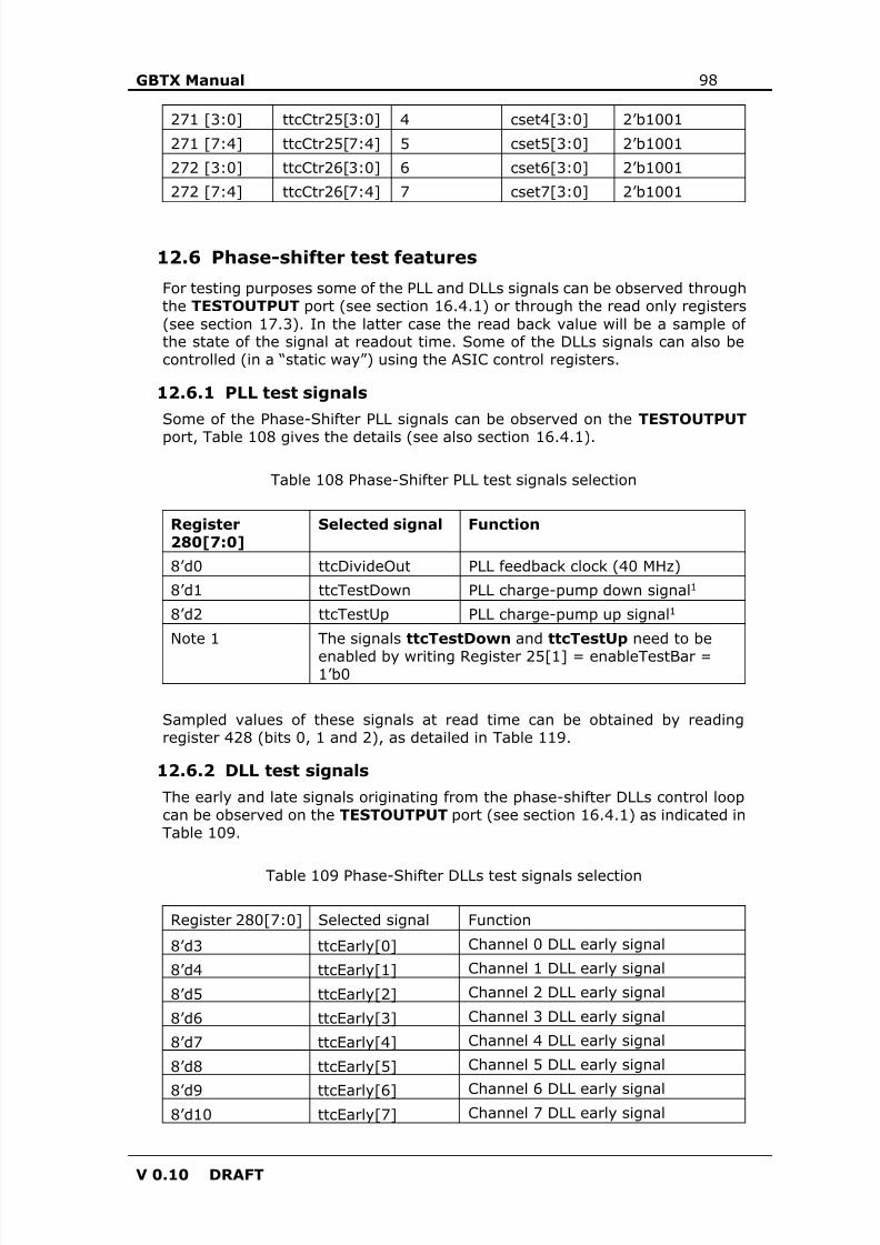
8/15/2019 gbtx Manual
http://slidepdf.com/reader/full/gbtx-manual 98/200
GBTX Manual 98
V 0.10 DRAFT
271 [3:0] ttcCtr25[3:0] 4 cset4[3:0] 2’b1001271 [7:4] ttcCtr25[7:4] 5 cset5[3:0] 2’b1001272 [3:0] ttcCtr26[3:0] 6 cset6[3:0] 2’b1001272 [7:4] ttcCtr26[7:4] 7 cset7[3:0] 2’b1001
12.6 Phase-shifter test features
For testing purposes some of the PLL and DLLs signals can be observed throughthe TESTOUTPUT port (see section 16.4.1) or through the read only registers(see section 17.3) . In the latter case the read back value will be a sample ofthe state of the signal at readout time. Some of the DLLs signals can also becontrolled (in a “static way”) using the ASIC control registers.
12.6.1 PLL test signals
Some of the Phase-Shifter PLL signals can be observed on the TESTOUTPUT port, Table 108 gives the details (see also section 16.4.1) .
Table 108 Phase-Shifter PLL test signals selection
Register280[7:0]
Selected signal Function
8’d0 ttcDivideOut PLL feedback clock (40 MHz)8’d1 ttcTestDown PLL charge-pump down signal 1 8’d2 ttcTestUp PLL charge-pump up signal 1 Note 1 The signals ttcTestDown and ttcTestUp need to be
enabled by writing Register 25[1] = enableTestBar =1’b0
Sampled values of these signals at read time can be obtained by readingregister 428 (bits 0, 1 and 2), as detailed in Table 119.
12.6.2 DLL test signals
The early and late signals originating from the phase-shifter DLLs control loopcan be observed on the TESTOUTPUT port (see section 16.4.1) as indicated inTable 109.
Table 109 Phase-Shifter DLLs test signals selection
Register 280[7:0] Selected signal Function
8’d3 ttcEarly[0] Channel 0 DLL early signal
8’d4 ttcEarly[1] Channel 1 DLL early signal
8’d5 ttcEarly[2] Channel 2 DLL early signal
8’d6 ttcEarly[3] Channel 3 DLL early signal
8’d7 ttcEarly[4] Channel 4 DLL early signal
8’d8 ttcEarly[5] Channel 5 DLL early signal
8’d9 ttcEarly[6] Channel 6 DLL early signal8’d10 ttcEarly[7] Channel 7 DLL early signal
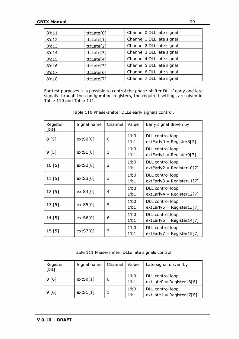
8/15/2019 gbtx Manual
http://slidepdf.com/reader/full/gbtx-manual 99/200
GBTX Manual 99
V 0.10 DRAFT
8’d11 ttcLate[0] Channel 0 DLL late signal
8’d12 ttcLate[1] Channel 1 DLL late signal
8’d13 ttcLate[2] Channel 2 DLL late signal
8’d14 ttcLate[3] Channel 3 DLL late signal
8’d15 ttcLate[4] Channel 4 DLL late signal8’d16 ttcLate[5] Channel 5 DLL late signal
8’d17 ttcLate[6] Channel 6 DLL late signal
8’d18 ttcLate[7] Channel 7 DLL late signal
For test purposes it is possible to control the phase-shifter DLLs’ early and latesignals through the configuration registers, the required settings are given inTable 110 and Table 111.
Table 110 Phase-shifter DLLs early signals control.
Register[bit]
Signal name Channel Value Early signal driven by
8 [5] extS0[0] 01’b01’b1
DLL control loopextEarly0 = Register8[7]
9 [5] extS1[0] 11’b01’b1
DLL control loopextEarly1 = Register9[7]
10 [5] extS2[0] 21’b01’b1
DLL control loopextEarly2 = Register10[7]
11 [5] extS3[0] 31’b01’b1
DLL control loopextEarly3 = Register11[7]
12 [5] extS4[0] 41’b01’b1
DLL control loopextEarly4 = Register12[7]
13 [5] extS5[0] 51’b01’b1
DLL control loopextEarly5 = Register13[7]
14 [5] extS6[0] 61’b01’b1
DLL control loopextEarly6 = Register14[7]
15 [5] extS7[0] 71’b01’b1
DLL control loopextEarly7 = Register15[7]
Table 111 Phase-shifter DLLs late signals control.
Register[bit]
Signal name Channel Value Late signal driven by
8 [6] extS0[1] 01’b01’b1
DLL control loopextLate0 = Register16[6]
9 [6] extS1[1] 11’b01’b1
DLL control loopextLate1 = Register17[6]
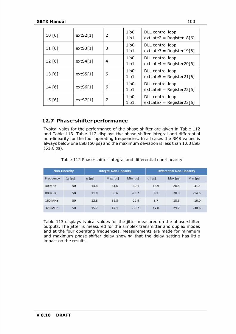
8/15/2019 gbtx Manual
http://slidepdf.com/reader/full/gbtx-manual 100/200
GBTX Manual 100
V 0.10 DRAFT
10 [6] extS2[1] 21’b01’b1
DLL control loopextLate2 = Register18[6]
11 [6] extS3[1] 31’b01’b1
DLL control loopextLate3 = Register19[6]
12 [6] extS4[1] 4 1’b01’b1
DLL control loopextLate4 = Register20[6]
13 [6] extS5[1] 51’b01’b1
DLL control loopextLate5 = Register21[6]
14 [6] extS6[1] 61’b01’b1
DLL control loopextLate6 = Register22[6]
15 [6] extS7[1] 71’b01’b1
DLL control loopextLate7 = Register23[6]
12.7 Phase-shifter performance
Typical vales for the performance of the phase-shifter are given in Table 112and Table 113. Table 112 displays the phase-shifter integral and differentialnon-linearity for the four operating frequencies. In all cases the RMS values isalways below one LSB (50 ps) and the maximum deviation is less than 1.03 LSB(51.6 ps).
Table 112 Phase-shifter integral and differential non-linearity
Table 113 displays typical values for the jitter measured on the phase-shifteroutputs. The jitter is measured for the simplex transmitter and duplex modesand at the four operating frequencies. Measurements are made for minimumand maximum phase-shifter delay showing that the delay setting has littleimpact on the results.
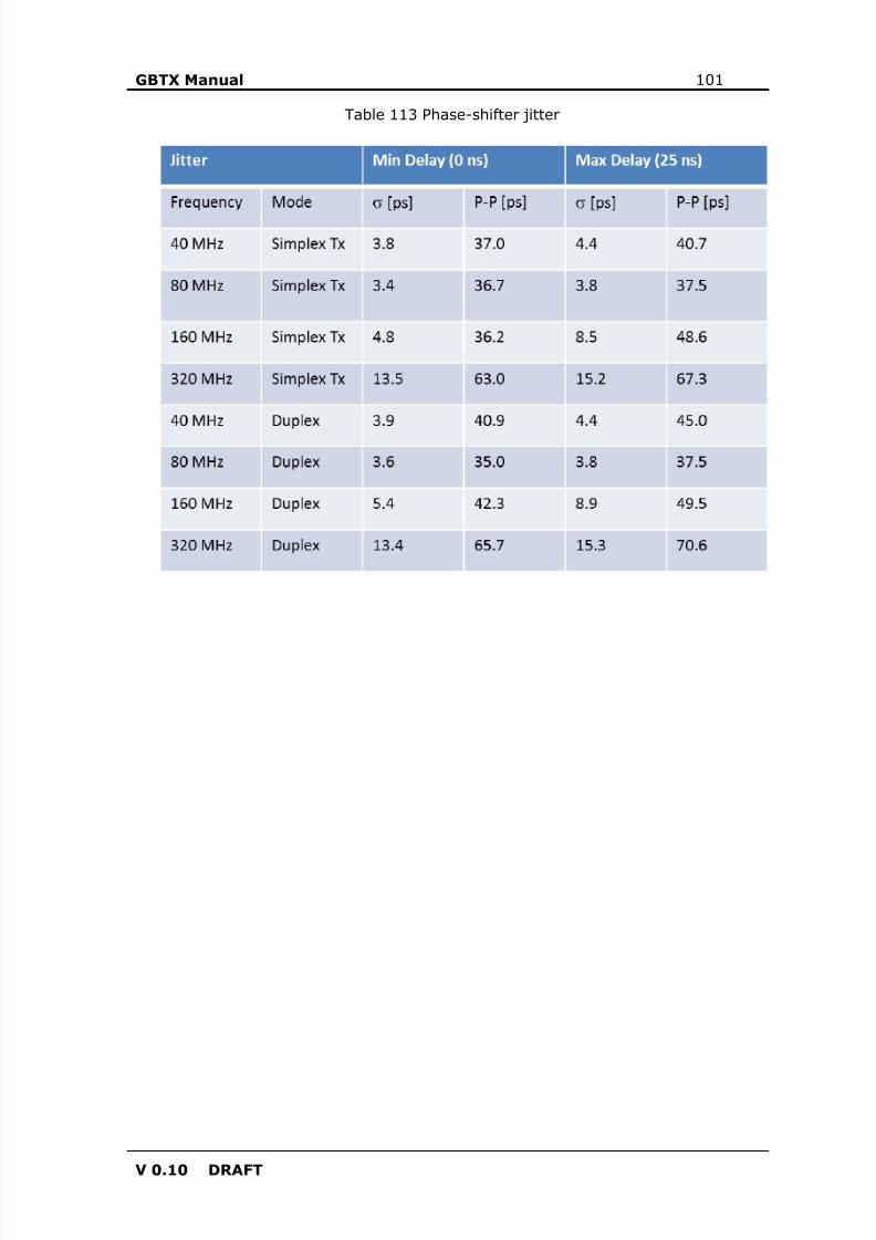
8/15/2019 gbtx Manual
http://slidepdf.com/reader/full/gbtx-manual 101/200
GBTX Manual 101
V 0.10 DRAFT
Table 113 Phase-shifter jitter
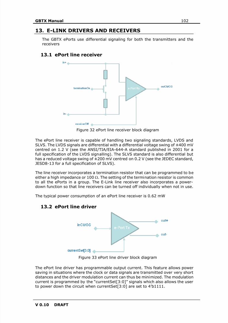
8/15/2019 gbtx Manual
http://slidepdf.com/reader/full/gbtx-manual 102/200
GBTX Manual 102
V 0.10 DRAFT
13. E-LINK DRIVERS AND RECEIVERS
The GBTX ePorts use differential signaling for both the transmitters and thereceivers
13.1
ePort line receiver
Figure 32 ePort line receiver block diagram
The ePort line receiver is capable of handling two signaling standards, LVDS andSLVS. The LVDS signals are differential with a differential voltage swing of ±400 mVcentred on 1.2 V (see the ANSI/TIA/EIA-644-A standard published in 2001 for afull specification of the LVDS signalling). The SLVS standard is also differential buthas a reduced voltage swing of ±200 mV centred on 0.2 V (see the JEDEC standard,JESD8-13 for a full specification of SLVS).
The line receiver incorporates a termination resistor that can be programmed to beeither a high impedance or 100 Ω . The setting of the termination resistor is commonto all the ePorts in a group. The E-Link line receiver also incorporates a power-down function so that line receivers can be turned off individually when not in use.
The typical power consumption of an ePort line receiver is 0.62 mW
13.2 ePort line driver
Figure 33 ePort line driver block diagram
The ePort line driver has programmable output current. This feature allows powersaving in situations where the clock or data signals are transmitted over very shortdistances and the driver modulation current can thus be minimized. The modulation
current is programmed by the “currentSet[3:0]” signals which also allows the userto power down the circuit when currentSet[3:0] are set to 4’b1111.
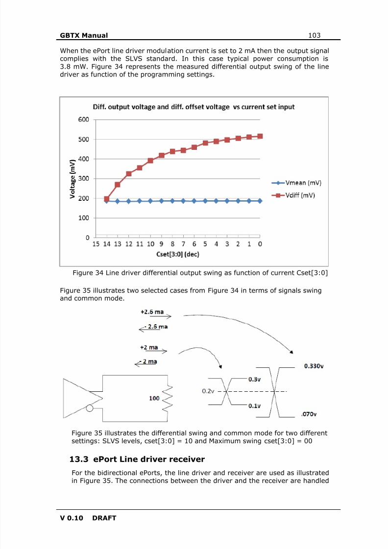
8/15/2019 gbtx Manual
http://slidepdf.com/reader/full/gbtx-manual 103/200
GBTX Manual 103
V 0.10 DRAFT
When the ePort line driver modulation current is set to 2 mA then the output signalcomplies with the SLVS standard. In this case typical power consumption is3.8 mW. Figure 34 represents the measured differential output swing of the linedriver as function of the programming settings.
Figure 34 Line driver differential output swing as function of current Cset[3:0]
Figure 35 illustrates two selected cases from Figure 34 in terms of signals swingand common mode.
Figure 35 illustrates the differential swing and common mode for two differentsettings: SLVS levels, cset[3:0] = 10 and Maximum swing cset[3:0] = 00
13.3 ePort Line driver receiver
For the bidirectional ePorts, the line driver and receiver are used as illustrated
in Figure 35. The connections between the driver and the receiver are handled
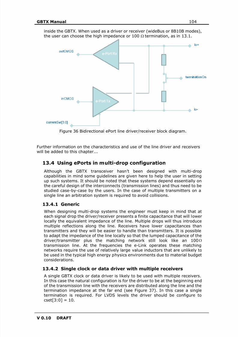
8/15/2019 gbtx Manual
http://slidepdf.com/reader/full/gbtx-manual 104/200
GBTX Manual 104
V 0.10 DRAFT
inside the GBTX. When used as a driver or receiver (wideBus or 8B10B modes),the user can choose the high impedance or 100 Ω termination, as in 13.1.
Figure 36 Bidirectional ePort line driver/receiver block diagram.
Further information on the characteristics and use of the line driver and receiverswill be added to this chapter...
13.4 Using ePorts in multi-drop configuration
Although the GBTX transceiver hasn’t been designed with multi-drop
capabilities in mind some guidelines are given here to help the user in settingup such systems. It should be noted that these systems depend essentially onthe careful design of the interconnects (transmission lines) and thus need to bestudied case-by-case by the users. In the case of multiple transmitters on asingle line an arbitration system is required to avoid collisions.
13.4.1 Generic
When designing multi-drop systems the engineer must keep in mind that ateach signal drop the driver/receiver presents a finite capacitance that will lowerlocally the equivalent impedance of the line. Multiple drops will thus introducemultiple reflections along the line. Receivers have lower capacitances thantransmitters and they will be easier to handle than transmitters. It is possible
to adapt the impedance of the line locally so that the lumped capacitance of thedriver/transmitter plus the matching network still look like an 100 Ω transmission line. At the frequencies the e-Link operates these matchingnetworks require the use of relatively large value inductors that are unlikely tobe used in the typical high energy physics environments due to material budgetconsiderations.
13.4.2 Single clock or data driver with multiple receivers
A single GBTX clock or data driver is likely to be used with multiple receivers.In this case the natural configuration is for the driver to be at the beginning endof the transmission line with the receivers are distributed along the line and thetermination impedance at the far end (see Figure 37) . In this case a single
termination is required. For LVDS levels the driver should be configure tocset[3:0] = 10.
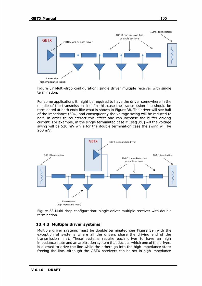
8/15/2019 gbtx Manual
http://slidepdf.com/reader/full/gbtx-manual 105/200
GBTX Manual 105
V 0.10 DRAFT
Figure 37 Multi-drop configuration: single driver multiple receiver with singletermination.
For some applications it might be required to have the driver somewhere in themiddle of the transmission line. In this case the transmission line should beterminated at both ends like what is shown in Figure 38. The driver will see halfof the impedance (50 Ω) and consequently the voltage swing will be reduced tohalf. In order to counteract this effect one can increase the buffer drivingcurrent. For example, in the single terminated case if Cset[3:0] =0 the voltageswing will be 520 mV while for the double termination case the swing will be260 mV.
Figure 38 Multi-drop configuration: single driver multiple receiver with doubletermination.
13.4.3 Multiple driver systems
Multiple driver systems must be double terminated see Figure 39 (with theexception of systems where all the drivers share the driving end of thetransmission line). These systems require each driver to have an highimpedance state and an arbitration system that decides which one of the driversis allowed to drive the line while the others go into the high impedance statefreeing the line. Although the GBTX receivers can be set in high impedance
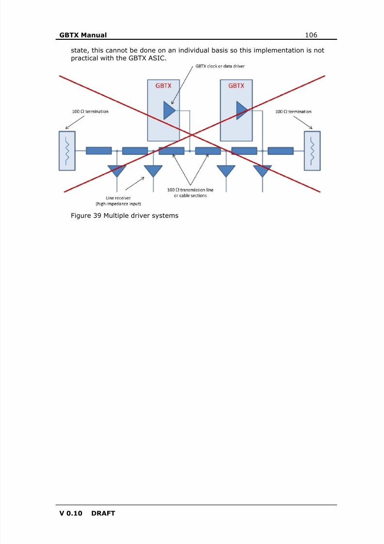
8/15/2019 gbtx Manual
http://slidepdf.com/reader/full/gbtx-manual 106/200
GBTX Manual 106
V 0.10 DRAFT
state, this cannot be done on an individual basis so this implementation is notpractical with the GBTX ASIC.
Figure 39 Multiple driver systems

8/15/2019 gbtx Manual
http://slidepdf.com/reader/full/gbtx-manual 107/200
GBTX Manual 107
V 0.10 DRAFT
14. REED-SOLOMON ENCODING, DATA SCRAMBLINGAND SEU PROTECTION
Detailed information will be added to this chapter on the Forward, scramblingalgorithms and on the detailed schemes used in the GBTX to protect against
SEU data transmission corruption...
8/15/2019 gbtx Manual
http://slidepdf.com/reader/full/gbtx-manual 108/200
GBTX Manual 108
V 0.10 DRAFT
15. E-FUSES
The GBTX is equipped with a number of E-fuses. Each of the bits of the 366write-able configuration registers has a corresponding E-fuse. The optimalconfiguration parameters of the GBTX can then be written into the fuse array.The transfer from fuses to configuration registers is done during the automaticpower-up sequence. This then allows the GBTX to self-configure into anoperational state after power-up.Each E-fuse connects to a node whose logical state can be sampled and storedin the corresponding register bit. By default, an un-programmed E-fuse will pullthis node down to logic 0. If the E-fuse is programmed, the node will be pulledup to logic 1.The sampling of the fuse values is handled automatically by the power-up statemachine. This can be optionally disabled and is described in chapter 10.
15.1 E-fuse addressing
The E-fuses are grouped into 8 fuses to correspond to the 8 bits of eachconfiguration register. Each group of fuses has a 16-bit address which is thesame as the address of the corresponding register as listed in Table 118. All ofthe 8 fuses in one group are programmed together.There are three special 8-bit fuses listed in Table 114 that are not connected toconfiguration registers. They can be programmed with the same procedure asthe others, and their values can be read via I2C or SC-IC using their fuseaddresses. One is called configFuse, and is used in the power-up sequencedescribed in chapter 10, and the other two are test fuses to allow testing of thefuse programming procedure. Their values are not used in any of the GBTXblocks.
Table 114 Special fuses
Fuseaddress(dec)
Fuse Address[15:8]
Fuse Address[7:0]
configFuse 366 00000001 01101110TestFuse1 367 00000001 01101111TestFuse2 368 00000001 01110000
15.2 E-fuse programming
Each 8-bit fuse is programmed using the I2C interface by first writing the 16-bit address (the same as the corresponding configuration register), loading the8-bit data pattern and then burning the fuses. The sequence is:1. Use I2C to load bits[7:0] of the fuse address into the following register:
fuseBlowAddressLSB[7:0] = Register 238[7:0] .2. Use I2C to load bits[15:8] of the fuse address into the following register:
fuseBlowAddressMSB[7:0] = Register 239[7:0] .3. Use I2C to load the 8-bit pattern to be programmed into the fuses into the
following register. Logic 1 will burn the fuse, logic 0 will not burn the fuse.fuseBlowData[7:0] = Register 240[7:0] .
4. Switch on EfusePower = 3.3V.5. Pulse EfuseProgramPulse for 200us.
After programming is complete, EfusePower should be connected to VDD.

8/15/2019 gbtx Manual
http://slidepdf.com/reader/full/gbtx-manual 109/200
GBTX Manual 109
V 0.10 DRAFT
8/15/2019 gbtx Manual
http://slidepdf.com/reader/full/gbtx-manual 110/200
GBTX Manual 110
V 0.10 DRAFT
16. TESTABILITY
Built in link test features are essential for evaluation, production and in systemtesting. Moreover, they allow standardized link tests procedures at the systemlevel. The GBTX offers a variety of link test features.
16.1 Data transmission testing
The GBTX transmitter can be programmed to transmit the following:• A fixed pattern: 80’hAABB BBAA AABB BBAA AABB;• A repeating and incrementing 16-bit count;• A pseudo random bit sequence with 2 7-1 run length.
The GBTX receiver can be set to count errors on the received data. In that case,the receiver expects to receive the fixed pattern: 80’hAABB BBAA AABB BBAAAABB and each word received is checked for reception errors. The receiver cancount up to 2 16 -1 errors which can be read from the status registers. The errorcount is not allowed to overflow and it is cleared each time the error count
feature is enabled.It should be noticed that, due the presence of the scrambler, when a fixedpattern is used to test the data transmission in fact a pseudo random sequenceis actually transmitted over the GBT frame. However, since the scrambler canbe bypassed it is also possible to send the “raw” fixed pattern imbedded in theGBT frame. Since the fixed pattern transmitted is DC balanced the receiver willhave no problem locking to the incoming data stream.Full details to be added later to the chapter...
16.2 Loopback tests
When the GBTX operates as a full link transceiver it is able to implementextensive loopback tests. These tests can be subdivided in receiver loopbacktests and transmitter loopback tests as shown in Figure 36. The former type ismainly for “in system testing”, while the latter is mainly for evaluation andproduction testing of the GBTX itself.Receiver loopbacks:
RLC: Testing of the SER and DES; RLB: Testing of the receiver chain from the de-serializer input up to the
decoder and the transmitter chain from the encoder up to the serializeroutput;
RLA: Testing of the receiver chain from the de-serializer input up to thede-scrambler output and testing of the transmitter chain from the
scrambler input up to serializer output.Transmitter loopback:
TLA: Testing of the transmitter and receiver I/O interface. TLB: Testing of the transmitter chain from the ePorts up to the scrambler
output and the receiver chain from the de-scrambler input to the ePorts. TLC: Testing of the transmitter chain from the ePorts up to the encoder
output and the receiver chain from the decoder input to the ePorts.
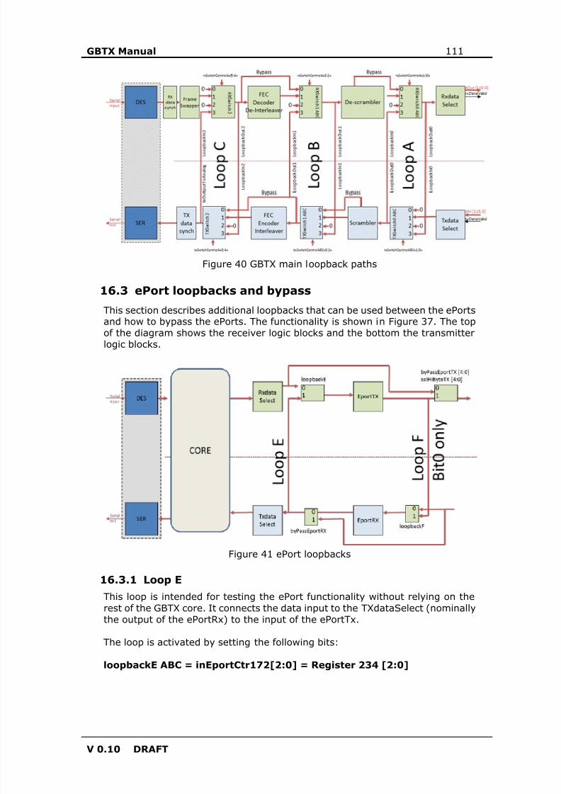
8/15/2019 gbtx Manual
http://slidepdf.com/reader/full/gbtx-manual 111/200
GBTX Manual 111
V 0.10 DRAFT
Figure 40 GBTX main loopback paths
16.3 ePort loopbacks and bypass
This section describes additional loopbacks that can be used between the ePortsand how to bypass the ePorts. The functionality is shown in Figure 37. The topof the diagram shows the receiver logic blocks and the bottom the transmitterlogic blocks.
Figure 41 ePort loopbacks
16.3.1 Loop E
This loop is intended for testing the ePort functionality without relying on therest of the GBTX core. It connects the data input to the TXdataSelect (nominallythe output of the ePortRx) to the input of the ePortTx.
The loop is activated by setting the following bits:
loopbackE ABC = inEportCtr172[2:0] = Register 234 [2:0]
8/15/2019 gbtx Manual
http://slidepdf.com/reader/full/gbtx-manual 112/200
GBTX Manual 112
V 0.10 DRAFT
16.3.2 Loop F
This loop is intended for testing the serialiser/deserialiser functions of theePorts. It allows the connection of ePortTx[0] to ePortRx[0]. Note that thisaffects only channel 0 of the ePorts.
The loop is activated by setting the following bits:
loopbackF ABC = inEportCtr172[5:3] = Register 234[5:3]
16.3.3 Bypass ePortRx
This allows a full bypass of the ePortRx block. The input data word receivedfrom the SLVS receivers (dataIn[39:0]) is connected directly to input of theGBTX core. In FEC mode, the GBTX core expects 80 bits of data, so dIn[39:0]is duplicated. When running in wideBus mode (112 bits of data), the extra databits (dInWideBusMode[15:0]) are also duplicated.The input data frames to the GBTX core (TXdata) are shown in the table below.
Table 115 Frame transmitted by the GBTX when the ePortRx circuit isbypassed
Mode Data frame FEC TXdata[79:0] = dIn[39:0], dIn[39:0]wideBus TXdata[111:0] = dIn[39:0], dIn[39:0], dInWideBusMode[15:0], dInWideBusMode[15:0]
Note that if the ePortRx bypass feature is to be used, then the ePortRx must beconfigured in 80 Mbit-mode. This ensures that all the SLVS receivers areenabled (in 160 or 320 Mbit modes, some receivers are automatically disabled).
The ePortRX bypass is activated by setting the following bits:
bypassEportRX ABC = inEportCtr190[2:0] = Register 252 [2:0]
16.3.4 Bypass ePortTx
This allows bypassing the ePortTx and connects the output signals from theGBTX core directly to the SLVS transmitters. This can be done for eachindividual ePort group. For a group, the eight SLVS transmitters are connectedto one byte of the sixteen bits allocated to that group, as described below.
Note that if the ePortTx bypass feature is to be used, then the ePortTx must be
configured in 80 Mbit-mode. This ensures that all the SLVS transmitters areenabled (in 160 or 320 Mbit modes, some transmitters are automaticallydisabled).
The ePortTx bypass per group [4:0] is activated by setting the following bits:
bypassEportTX0 ABC = inEportCtr184[2:0] = Register 246 [2:0]bypassEportTX1 ABC = inEportCtr184[5:3] = Register 246 [5:3]bypassEportTX2 ABC = inEportCtr185[0], inEportCtr184[7:6]
= Register 247 [0], Register 246 [7:6]bypassEportTX3 ABC = inEportCtr185[3:1] = Register 247 [3:1]bypassEportTX4 ABC = inEportCtr185[6:4] = Register 247 [6:4]
8/15/2019 gbtx Manual
http://slidepdf.com/reader/full/gbtx-manual 113/200
8/15/2019 gbtx Manual
http://slidepdf.com/reader/full/gbtx-manual 114/200
GBTX Manual 114
V 0.10 DRAFT
Register280value
Register280value
Register280value
0 ttcDivideOut 49 channelLockedGroup1[0] 98 powerUpFSMState[0]1 ttcTestDown 50 channelLockedGroup1[1] 99 powerUpFSMState[1]2 ttcTestUp 51 channelLockedGroup1[2] 100 powerUpFSMState[2]3 ttcEarly[0] 52 channelLockedGroup1[3] 101 powerUpFSMState[3]4 ttcEarly[1] 53 channelLockedGroup1[4] 102 powerUpFSMState[4]5 ttcEarly[2] 54 channelLockedGroup1[5] 103 EportDataTXA[32]6 ttcEarly[3] 55 channelLockedGroup1[6] 104 EportDataTXA[33]7 ttcEarly[4] 56 channelLockedGroup1[7] 105 EportDataTXA[34]8 ttcEarly[5] 57 channelLockedGroup2[0] 106 EportDataTXA[35]9 ttcEarly[6] 58 channelLockedGroup2[1] 107 EportDataTXA[36]
10 ttcEarly[7] 59 channelLockedGroup2[2] 108 EportDataTXA[37]11 ttcLate[0] 60 channelLockedGroup2[3] 109 EportDataTXA[38]12 ttcLate[1] 61 channelLockedGroup2[4] 110 EportDataTXA[39]
13 ttcLate[2] 62 channelLockedGroup2[5] 111 EportDataTXA[48]14 ttcLate[3] 63 channelLockedGroup2[6] 112 EportDataTXA[49]15 ttcLate[4] 64 channelLockedGroup2[7] 113 EportDataTXA[50]16 ttcLate[5] 65 channelLockedGroup3[0] 114 EportDataTXA[51]17 ttcLate[6] 66 channelLockedGroup3[1] 115 EportDataTXA[52]18 ttcLate[7] 67 channelLockedGroup3[2] 116 EportDataTXA[53]19 txTestUp 68 channelLockedGroup3[3] 117 EportDataTXA[54]20 txTestDown 69 channelLockedGroup3[4] 118 EportDataTXA[55]21 SLVSinTest 70 channelLockedGroup3[5] 119 EportDataTXA[64]22 ePLLRXInstantLock 71 channelLockedGroup3[6] 120 EportDataTXA[65]23 ePLLTXInstantLock 72 channelLockedGroup3[7] 121 EportDataTXA[66]24 xPllInstantLock 73 channelLockedGroup4[0] 122 EportDataTXA[67]
25 txInstantLockGated 74 channelLockedGroup4[1] 123 EportDataTXA[68]26 rxInstantLockRefGated 75 channelLockedGroup4[2] 124 EportDataTXA[69]27 RXEPLLLocked 76 channelLockedGroup4[3] 125 EportDataTXA[70]28 TXEPLLLocked 77 channelLockedGroup4[4] 126 EportDataTXA[71]29 XPLLLocked 78 channelLockedGroup4[5] 127 EportDataTXA[80]30 txReady_control 79 channelLockedGroup4[6] 128 EportDataTXA[81]31 rxReady_control 80 channelLockedGroup4[7] 129 EportDataTXA[82]32 dllLockedGroup[0] 81 channelLockedGroup5[0] 130 EportDataTXA[83]33 dllLockedGroup[1] 82 channelLockedGroup5[1] 131 EportDataTXA[84]34 dllLockedGroup[2] 83 channelLockedGroup5[2] 132 EportDataTXA[85]35 dllLockedGroup[3] 84 channelLockedGroup5[3] 133 EportDataTXA[86]36 dllLockedGroup[4] 85 channelLockedGroup5[4] 134 EportDataTXA[87]37 dllLockedGroup[5] 86 channelLockedGroup5[5] 135 EportDataTXA[96]38 dllLockedGroup[6]: 87 channelLockedGroup5[6] 136 EportDataTXA[97]39 1'b0 88 channelLockedGroup5[7] 137 EportDataTXA[98]40 dllLockedEc 89 channelLockedGroup6[0] 138 EportDataTXA[99]41 channelLockedGroup0[0] 90 channelLockedGroup6[1] 139 EportDataTXA[100]42 channelLockedGroup0[1] 91 channelLockedGroup6[2] 140 EportDataTXA[101]43 channelLockedGroup0[2] 92 channelLockedGroup6[3] 141 EportDataTXA[102]44 channelLockedGroup0[3] 93 channelLockedGroup6[4] 142 EportDataTXA[103]45 channelLockedGroup0[4] 94 channelLockedGroup6[5] 143 headerInPhase46 channelLockedGroup0[5] 95 channelLockedGroup6[6] 144 headerInAntiPhase47 channelLockedGroup0[6] 96 channelLockedGroup6[7] 145 rxSkipCycle48 channelLockedGroup0[7] 97 channelLockedEc 146 rxSelectDataInPhase
8/15/2019 gbtx Manual
http://slidepdf.com/reader/full/gbtx-manual 115/200
GBTX Manual 115
V 0.10 DRAFT
16.4.2 Test Clock Output
The output pad testClockOut can be connected to one of a number ofdifferent signals from the clock manager. These are selected by the followingconfiguration register:
cmTestMuxSelect[4:0] = ckCtr50[4:0] = Register 319[4:0]
The signals are listed below, together with the corresponding value of register319[4:0], in decimal.
Register 319 [4:0] Selected signal0 iCmTestOut :1 sampleRx4080A :2 sampleRx40160A3 sampleRx40320A4 sampleRx4040AB5 sampleRx4040AC
6 sampleRx4080B :7 sampleRx40160B8 sampleRx40320B9 sampleRx4040BA10 sampleRx4040BC11 sampleRx4080C12 sampleRx40160C13 sampleRx40320C14 sampleRx4040CA15 sampleRx4040CB16 sampleTx4080A17 sampleTx40160A18 sampleTx40320A19 sampleTx4040AB20 sampleTx4040AC21 sampleTx4080B22 sampleTx40160B23 sampleTx40320B24 sampleTx4040BA25 sampleTx4040BC26 sampleTx4080C27 sampleTx40160C28 sampleTx40320C29 sampleTx4040CA30 sampleTx4040CB
The signal selected by register 319[7:0] = 0 (iCmTestOut) can be connectedto one of another selection of signals. The signal can be selected with theflowing configuration register:
cmTestOutSelect[6:0] = ckCtr14[6:0] = Register 283[6:0].
The signals are listed in the table below according to the setting of register283, in decimal.

8/15/2019 gbtx Manual
http://slidepdf.com/reader/full/gbtx-manual 116/200
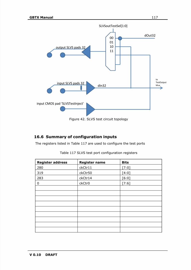
8/15/2019 gbtx Manual
http://slidepdf.com/reader/full/gbtx-manual 117/200
8/15/2019 gbtx Manual
http://slidepdf.com/reader/full/gbtx-manual 118/200
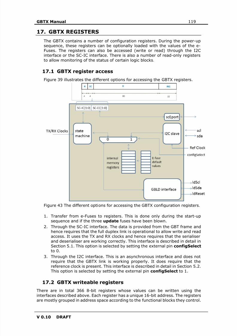
8/15/2019 gbtx Manual
http://slidepdf.com/reader/full/gbtx-manual 119/200
GBTX Manual 119
V 0.10 DRAFT
17. GBTX REGISTERS
The GBTX contains a number of configuration registers. During the power-upsequence, these registers can be optionally loaded with the values of the e-Fuses. The registers can also be accessed (write or read) through the I2Cinterface or the SC-IC interface. There is also a number of read-only registersto allow monitoring of the status of certain logic blocks.
17.1 GBTX register access
Figure 39 illustrates the different options for accessing the GBTX registers.
Figure 43 The different options for accessing the GBTX configuration registers.
1. Transfer from e-Fuses to registers. This is done only during the start-upsequence and if the three update fuses have been blown.
2. Through the SC-IC interface. The data is provided from the GBT frame andhence requires that the full duplex link is operational to allow write and readaccess. It uses the TX and RX clocks and hence requires that the serialiserand deserialiser are working correctly. This interface is described in detail inSection 5.1. This option is selected by setting the external pin configSelect to 0.
3. Through the I2C interface. This is an asynchronous interface and does notrequire that the GBTX link is working properly. It does require that thereference clock is present. This interface is described in detail in Section 5.2. This option is selected by setting the external pin configSelect to 1.
17.2 GBTX writeable registers
There are in total 366 8-bit registers whose values can be written using theinterfaces described above. Each register has a unique 16-bit address. The registersare mostly grouped in address space according to the functional blocks they control.
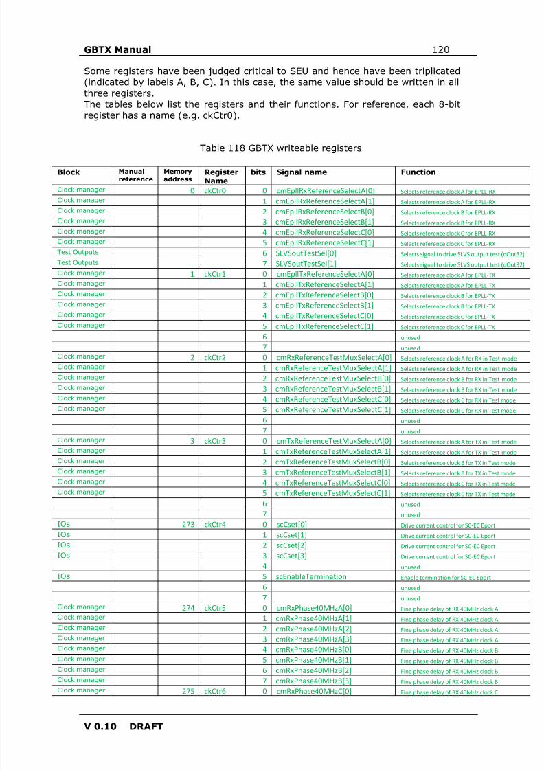
8/15/2019 gbtx Manual
http://slidepdf.com/reader/full/gbtx-manual 120/200
GBTX Manual 120
V 0.10 DRAFT
Some registers have been judged critical to SEU and hence have been triplicated(indicated by labels A, B, C). In this case, the same value should be written in allthree registers.The tables below list the registers and their functions. For reference, each 8-bitregister has a name (e.g. ckCtr0).
Table 118 GBTX writeable registers
Block Manualreference
Memoryaddress
RegisterName
bits Signal name Function
Clock manager 0 ckCtr0 0 cmEpllRxReferenceSelectA[0] Selects reference clock A for EPLL-RXClock manager 1 cmEpllRxReferenceSelectA[1] Selects reference clock A for EPLL-RXClock manager 2 cmEpllRxReferenceSelectB[0] Selects reference clock B for EPLL-RXClock manager 3 cmEpllRxReferenceSelectB[1] Selects reference clock B for EPLL-RXClock manager 4 cmEpllRxReferenceSelectC[0] Selects reference clock C for EPLL-RXClock manager 5 cmEpllRxReferenceSelectC[1] Selects reference clock C for EPLL-RXTest Outputs 6 SLVSoutTestSel[0] Selects signal to drive SLVS output test (dOut32)Test Outputs 7 SLVSoutTestSel[1] Selects signal to drive SLVS output test (dOut32)Clock manager 1 ckCtr1 0 cmEpllTxReferenceSelectA[0] Selects reference clock A for EPLL-TXClock manager 1 cmEpllTxReferenceSelectA[1] Selects reference clock A for EPLL-TXClock manager 2 cmEpllTxReferenceSelectB[0] Selects reference clock B for EPLL-TXClock manager 3 cmEpllTxReferenceSelectB[1] Selects reference clock B for EPLL-TXClock manager 4 cmEpllTxReferenceSelectC[0] Selects reference clock C for EPLL-TXClock manager 5 cmEpllTxReferenceSelectC[1] Selects reference clock C for EPLL-TX
6 unused
7 unusedClock manager 2 ckCtr2 0 cmRxReferenceTestMuxSelectA[0] Selects reference clock A for RX in Test modeClock manager 1 cmRxReferenceTestMuxSelectA[1] Selects reference clock A for RX in Test modeClock manager 2 cmRxReferenceTestMuxSelectB[0] Selects reference clock B for RX in Test modeClock manager 3 cmRxReferenceTestMuxSelectB[1] Selects reference clock B for RX in Test modeClock manager 4 cmRxReferenceTestMuxSelectC[0] Selects reference clock C for RX in Test modeClock manager 5 cmRxReferenceTestMuxSelectC[1] Selects reference clock C for RX in Test mode
6 unused
7 unusedClock manager 3 ckCtr3 0 cmTxReferenceTestMuxSelectA[0] Selects reference clock A for TX in Test modeClock manager 1 cmTxReferenceTestMuxSelectA[1] Selects reference clock A for TX in Test modeClock manager 2 cmTxReferenceTestMuxSelectB[0] Selects reference clock B for TX in Test modeClock manager 3 cmTxReferenceTestMuxSelectB[1] Selects reference clock B for TX in Test modeClock manager 4 cmTxReferenceTestMuxSelectC[0] Selects reference clock C for TX in Test modeClock manager 5 cmTxReferenceTestMuxSelectC[1] Selects reference clock C for TX in Test mode
6 unused
7 unused
IOs 273 ckCtr4 0 scCset[0] Drive current control for SC-EC Eport
IOs 1 scCset[1] Drive current control for SC-EC Eport
IOs 2 scCset[2] Drive current control for SC-EC Eport
IOs 3 scCset[3] Drive current control for SC-EC Eport
4 unused
IOs 5 scEnableTermination Enable termination for SC-EC Eport
6 unused
7 unusedClock manager 274 ckCtr5 0 cmRxPhase40MHzA[0] Fine phase delay of RX 40MHz clock AClock manager 1 cmRxPhase40MHzA[1] Fine phase delay of RX 40MHz clock AClock manager 2 cmRxPhase40MHzA[2] Fine phase delay of RX 40MHz clock AClock manager 3 cmRxPhase40MHzA[3] Fine phase delay of RX 40MHz clock AClock manager 4 cmRxPhase40MHzB[0] Fine phase delay of RX 40MHz clock BClock manager 5 cmRxPhase40MHzB[1] Fine phase delay of RX 40MHz clock BClock manager 6 cmRxPhase40MHzB[2] Fine phase delay of RX 40MHz clock BClock manager 7 cmRxPhase40MHzB[3] Fine phase delay of RX 40MHz clock BClock manager 275 ckCtr6 0 cmRxPhase40MHzC[0] Fine phase delay of RX 40MHz clock C
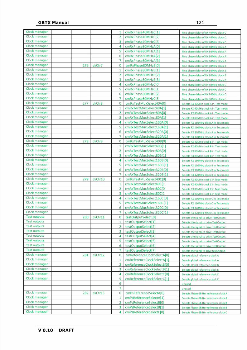
8/15/2019 gbtx Manual
http://slidepdf.com/reader/full/gbtx-manual 121/200
GBTX Manual 121
V 0.10 DRAFT
Clock manager 1 cmRxPhase40MHzC[1] Fine phase delay of RX 40MHz clock CClock manager 2 cmRxPhase40MHzC[2] Fine phase delay of RX 40MHz clock CClock manager 3 cmRxPhase40MHzC[3] Fine phase delay of RX 40MHz clock CClock manager 4 cmRxPhase80MHzA[0] Fine phase delay of RX 80MHz clock AClock manager 5 cmRxPhase80MHzA[1] Fine phase delay of RX 80MHz clock AClock manager 6 cmRxPhase80MHzA[2] Fine phase delay of RX 80MHz clock A
Clock manager 7 cmRxPhase80MHzA[3] Fine phase delay of RX 80MHz clock AClock manager 276 ckCtr7 0 cmRxPhase80MHzB[0] Fine phase delay of RX 80MHz clock BClock manager 1 cmRxPhase80MHzB[1] Fine phase delay of RX 80MHz clock BClock manager 2 cmRxPhase80MHzB[2] Fine phase delay of RX 80MHz clock BClock manager 3 cmRxPhase80MHzB[3] Fine phase delay of RX 80MHz clock BClock manager 4 cmRxPhase80MHzC[0] Fine phase delay of RX 80MHz clock CClock manager 5 cmRxPhase80MHzC[1] Fine phase delay of RX 80MHz clock CClock manager 6 cmRxPhase80MHzC[2] Fine phase delay of RX 80MHz clock CClock manager 7 cmRxPhase80MHzC[3] Fine phase delay of RX 80MHz clock CClock manager 277 ckCtr8 0 cmRxTestMuxSelect40A[0] Selects RX 40MHz clock A in Test modeClock manager 1 cmRxTestMuxSelect40A[1] Selects RX 40MHz clock A in Test modeClock manager 2 cmRxTestMuxSelect80A[0] Selects RX 80MHz clock A in Test modeClock manager 3 cmRxTestMuxSelect80A[1] Selects RX 80MHz clock A in Test mode
Clock manager 4 cmRxTestMuxSelect160A[0] Selects RX 160MHz clock A in Test modeClock manager 5 cmRxTestMuxSelect160A[1] Selects RX 160MHz clock A in Test modeClock manager 6 cmRxTestMuxSelect320A[0] Selects RX 320MHz clock A in Test modeClock manager 7 cmRxTestMuxSelect320A[1] Selects RX 320MHz clock A in Test modeClock manager 278 ckCtr9 0 cmRxTestMuxSelect40B[0] Selects RX 40MHz clock B in Test modeClock manager 1 cmRxTestMuxSelect40B[1] Selects RX 40MHz clock B in Test modeClock manager 2 cmRxTestMuxSelect80B[0] Selects RX 80MHz clock B in Test modeClock manager 3 cmRxTestMuxSelect80B[1] Selects RX 80MHz clock B in Test modeClock manager 4 cmRxTestMuxSelect160B[0] Selects RX 160MHz clock B in Test modeClock manager 5 cmRxTestMuxSelect160B[1] Selects RX 160MHz clock B in Test modeClock manager 6 cmRxTestMuxSelect320B[0] Selects RX 320MHz clock B in Test modeClock manager 7 cmRxTestMuxSelect320B[1] Selects RX 320MHz clock B in Test modeClock manager 279 ckCtr10 0 cmRxTestMuxSelect40C[0] Selects RX 40MHz clock C in Test mode
Clock manager 1 cmRxTestMuxSelect40C[1] Selects RX 40MHz clock C in Test modeClock manager 2 cmRxTestMuxSelect80C[0] Selects RX 80MHz clock C in Test modeClock manager 3 cmRxTestMuxSelect80C[1] Selects RX 80MHz clock C in Test modeClock manager 4 cmRxTestMuxSelect160C[0] Selects RX 160MHz clock C in Test modeClock manager 5 cmRxTestMuxSelect160C[1] Selects RX 160MHz clock C in Test modeClock manager 6 cmRxTestMuxSelect320C[0] Selects RX 320MHz clock C in Test modeClock manager 7 cmRxTestMuxSelect320C[1] Selects RX 320MHz clock C in Test modeTest outputs 280 ckCtr11 0 testOutputSelect[0] Selects the signal to drive TestOutputTest outputs 1 testOutputSelect[1] Selects the signal to drive TestOutputTest outputs 2 testOutputSelect[2] Selects the signal to drive TestOutputTest outputs 3 testOutputSelect[3] Selects the signal to drive TestOutputTest outputs 4 testOutputSelect[4] Selects the signal to drive TestOutputTest outputs 5 testOutputSelect[5] Selects the signal to drive TestOutput
Test outputs 6 testOutputSelect[6] Selects the signal to drive TestOutputTest outputs 7 testOutputSelect[7] Selects the signal to drive testOutputClock manager 281 ckCtr12 0 cmReferenceClockSelectA[0] Selects global reference clock AClock manager 1 cmReferenceClockSelectA[1] Selects global reference clock AClock manager 2 cmReferenceClockSelectB[0] Selects global reference clock BClock manager 3 cmReferenceClockSelectB[1] Selects global reference clock BClock manager 4 cmReferenceClockSelectC[0] Selects global reference clock CClock manager 5 cmReferenceClockSelectC[1] Selects global reference clock C
6 unused
7 unusedClock manager 282 ckCtr13 0 cmPsReferenceSelectA[0] Selects Phase-Shifter reference clock AClock manager 1 cmPsReferenceSelectA[1] Selects Phase-Shifter reference clock AClock manager 2 cmPsReferenceSelectB[0] Selects Phase-Shifter reference clock B
Clock manager 3 cmPsReferenceSelectB[1] Selects Phase-Shifter reference clock BClock manager 4 cmPsReferenceSelectC[0] Selects Phase-Shifter reference clock C
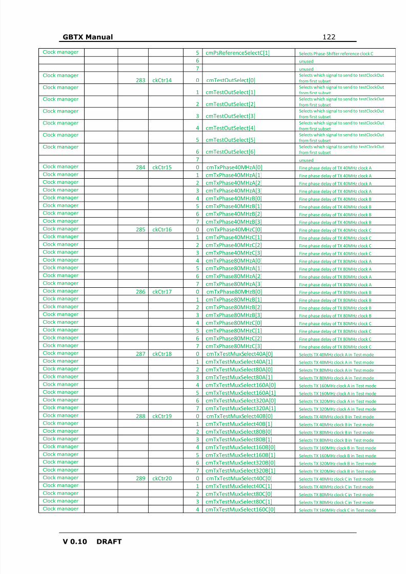
8/15/2019 gbtx Manual
http://slidepdf.com/reader/full/gbtx-manual 122/200
GBTX Manual 122
V 0.10 DRAFT
Clock manager 5 cmPsReferenceSelectC[1] Selects Phase-Shifter reference clock C
6 unused
7 unusedClock manager
283 ckCtr14 0 cmTestOutSelect[0]Selects which signal to send to testClockOutfrom first subset
Clock manager 1 cmTestOutSelect[1]
Selects which signal to send to testClockOutfrom first subset
Clock manager 2 cmTestOutSelect[2] Selects which signal to send to testClockOutfrom first subsetClock manager
3 cmTestOutSelect[3]Selects which signal to send to testClockOutfrom first subset
Clock manager 4 cmTestOutSelect[4]
Selects which signal to send to testClockOutfrom first subset
Clock manager 5 cmTestOutSelect[5]
Selects which signal to send to testClockOutfrom first subset
Clock manager 6 cmTestOutSelect[6]
Selects which signal to send to testClockOutfrom first subset
7 unusedClock manager 284 ckCtr15 0 cmTxPhase40MHzA[0] Fine phase delay of TX 40MHz clock AClock manager 1 cmTxPhase40MHzA[1] Fine phase delay of TX 40MHz clock AClock manager 2 cmTxPhase40MHzA[2] Fine phase delay of TX 40MHz clock AClock manager 3 cmTxPhase40MHzA[3] Fine phase delay of TX 40MHz clock AClock manager
4 cmTxPhase40MHzB[0] Fine phase delay of TX 40MHz clock BClock manager 5 cmTxPhase40MHzB[1] Fine phase delay of TX 40MHz clock BClock manager 6 cmTxPhase40MHzB[2] Fine phase delay of TX 40MHz clock BClock manager 7 cmTxPhase40MHzB[3] Fine phase delay of TX 40MHz clock BClock manager 285 ckCtr16 0 cmTxPhase40MHzC[0] Fine phase delay of TX 40MHz clock CClock manager 1 cmTxPhase40MHzC[1] Fine phase delay of TX 40MHz clock CClock manager 2 cmTxPhase40MHzC[2] Fine phase delay of TX 40MHz clock CClock manager 3 cmTxPhase40MHzC[3] Fine phase delay of TX 40MHz clock CClock manager 4 cmTxPhase80MHzA[0] Fine phase delay of TX 80MHz clock AClock manager 5 cmTxPhase80MHzA[1] Fine phase delay of TX 80MHz clock AClock manager 6 cmTxPhase80MHzA[2] Fine phase delay of TX 80MHz clock AClock manager 7 cmTxPhase80MHzA[3] Fine phase delay of TX 80MHz clock AClock manager 286 ckCtr17 0 cmTxPhase80MHzB[0] Fine phase delay of TX 80MHz clock BClock manager
1 cmTxPhase80MHzB[1] Fine phase delay of TX 80MHz clock BClock manager 2 cmTxPhase80MHzB[2] Fine phase delay of TX 80MHz clock BClock manager 3 cmTxPhase80MHzB[3] Fine phase delay of TX 80MHz clock BClock manager 4 cmTxPhase80MHzC[0] Fine phase delay of TX 80MHz clock CClock manager 5 cmTxPhase80MHzC[1] Fine phase delay of TX 80MHz clock CClock manager 6 cmTxPhase80MHzC[2] Fine phase delay of TX 80MHz clock CClock manager 7 cmTxPhase80MHzC[3] Fine phase delay of TX 80MHz clock CClock manager 287 ckCtr18 0 cmTxTestMuxSelect40A[0] Selects TX 40MHz clock A in Test modeClock manager 1 cmTxTestMuxSelect40A[1] Selects TX 40MHz clock A in Test modeClock manager 2 cmTxTestMuxSelect80A[0] Selects TX 80MHz clock A in Test modeClock manager 3 cmTxTestMuxSelect80A[1] Selects TX 80MHz clock A in Test modeClock manager 4 cmTxTestMuxSelect160A[0] Selects TX 160MHz clock A in Test modeClock manager 5 cmTxTestMuxSelect160A[1] Selects TX 160MHz clock A in Test modeClock manager
6 cmTxTestMuxSelect320A[0] Selects TX 320MHz clock A in Test modeClock manager 7 cmTxTestMuxSelect320A[1] Selects TX 320MHz clock A in Test modeClock manager 288 ckCtr19 0 cmTxTestMuxSelect40B[0] Selects TX 40MHz clock B in Test modeClock manager 1 cmTxTestMuxSelect40B[1] Selects TX 40MHz clock B in Test modeClock manager 2 cmTxTestMuxSelect80B[0] Selects TX 80MHz clock B in Test modeClock manager 3 cmTxTestMuxSelect80B[1] Selects TX 80MHz clock B in Test modeClock manager 4 cmTxTestMuxSelect160B[0] Selects TX 160MHz clock B in Test modeClock manager 5 cmTxTestMuxSelect160B[1] Selects TX 160MHz clock B in Test modeClock manager 6 cmTxTestMuxSelect320B[0] Selects TX 320MHz clock B in Test modeClock manager 7 cmTxTestMuxSelect320B[1] Selects TX 320MHz clock B in Test modeClock manager 289 ckCtr20 0 cmTxTestMuxSelect40C[0] Selects TX 40MHz clock C in Test modeClock manager 1 cmTxTestMuxSelect40C[1] Selects TX 40MHz clock C in Test modeClock manager 2 cmTxTestMuxSelect80C[0] Selects TX 80MHz clock C in Test mode
Clock manager 3 cmTxTestMuxSelect80C[1] Selects TX 80MHz clock C in Test modeClock manager 4 cmTxTestMuxSelect160C[0] Selects TX 160MHz clock C in Test mode
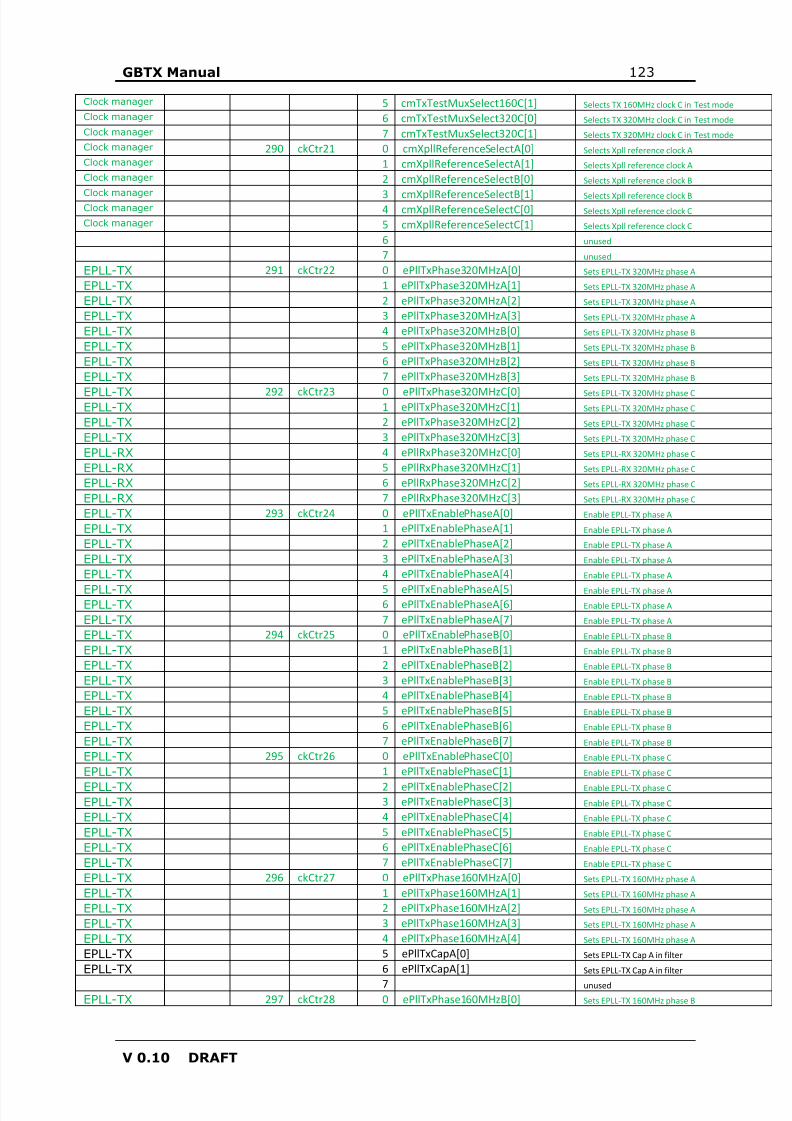
8/15/2019 gbtx Manual
http://slidepdf.com/reader/full/gbtx-manual 123/200
GBTX Manual 123
V 0.10 DRAFT
Clock manager 5 cmTxTestMuxSelect160C[1] Selects TX 160MHz clock C in Test modeClock manager 6 cmTxTestMuxSelect320C[0] Selects TX 320MHz clock C in Test modeClock manager 7 cmTxTestMuxSelect320C[1] Selects TX 320MHz clock C in Test modeClock manager 290 ckCtr21 0 cmXpllReferenceSelectA[0] Selects Xpll reference clock AClock manager 1 cmXpllReferenceSelectA[1] Selects Xpll reference clock AClock manager 2 cmXpllReferenceSelectB[0] Selects Xpll reference clock B
Clock manager 3 cmXpllReferenceSelectB[1] Selects Xpll reference clock BClock manager 4 cmXpllReferenceSelectC[0] Selects Xpll reference clock CClock manager 5 cmXpllReferenceSelectC[1] Selects Xpll reference clock C
6 unused
7 unused
EPLL-TX 291 ckCtr22 0 ePllTxPhase320MHzA[0] Sets EPLL-TX 320MHz phase A
EPLL-TX 1 ePllTxPhase320MHzA[1] Sets EPLL-TX 320MHz phase A
EPLL-TX 2 ePllTxPhase320MHzA[2] Sets EPLL-TX 320MHz phase A
EPLL-TX 3 ePllTxPhase320MHzA[3] Sets EPLL-TX 320MHz phase A
EPLL-TX 4 ePllTxPhase320MHzB[0] Sets EPLL-TX 320MHz phase B
EPLL-TX 5 ePllTxPhase320MHzB[1] Sets EPLL-TX 320MHz phase B
EPLL-TX 6 ePllTxPhase320MHzB[2] Sets EPLL-TX 320MHz phase B
EPLL-TX 7 ePllTxPhase320MHzB[3] Sets EPLL-TX 320MHz phase B
EPLL-TX 292 ckCtr23 0 ePllTxPhase320MHzC[0] Sets EPLL-TX 320MHz phase CEPLL-TX 1 ePllTxPhase320MHzC[1] Sets EPLL-TX 320MHz phase C
EPLL-TX 2 ePllTxPhase320MHzC[2] Sets EPLL-TX 320MHz phase C
EPLL-TX 3 ePllTxPhase320MHzC[3] Sets EPLL-TX 320MHz phase C
EPLL-RX 4 ePllRxPhase320MHzC[0] Sets EPLL-RX 320MHz phase C
EPLL-RX 5 ePllRxPhase320MHzC[1] Sets EPLL-RX 320MHz phase C
EPLL-RX 6 ePllRxPhase320MHzC[2] Sets EPLL-RX 320MHz phase C
EPLL-RX 7 ePllRxPhase320MHzC[3] Sets EPLL-RX 320MHz phase C
EPLL-TX 293 ckCtr24 0 ePllTxEnablePhaseA[0] Enable EPLL-TX phase A
EPLL-TX 1 ePllTxEnablePhaseA[1] Enable EPLL-TX phase A
EPLL-TX 2 ePllTxEnablePhaseA[2] Enable EPLL-TX phase A
EPLL-TX 3 ePllTxEnablePhaseA[3] Enable EPLL-TX phase A
EPLL-TX 4 ePllTxEnablePhaseA[4] Enable EPLL-TX phase A
EPLL-TX 5 ePllTxEnablePhaseA[5] Enable EPLL-TX phase AEPLL-TX 6 ePllTxEnablePhaseA[6] Enable EPLL-TX phase A
EPLL-TX 7 ePllTxEnablePhaseA[7] Enable EPLL-TX phase A
EPLL-TX 294 ckCtr25 0 ePllTxEnablePhaseB[0] Enable EPLL-TX phase B
EPLL-TX 1 ePllTxEnablePhaseB[1] Enable EPLL-TX phase B
EPLL-TX 2 ePllTxEnablePhaseB[2] Enable EPLL-TX phase B
EPLL-TX 3 ePllTxEnablePhaseB[3] Enable EPLL-TX phase B
EPLL-TX 4 ePllTxEnablePhaseB[4] Enable EPLL-TX phase B
EPLL-TX 5 ePllTxEnablePhaseB[5] Enable EPLL-TX phase B
EPLL-TX 6 ePllTxEnablePhaseB[6] Enable EPLL-TX phase B
EPLL-TX 7 ePllTxEnablePhaseB[7] Enable EPLL-TX phase B
EPLL-TX 295 ckCtr26 0 ePllTxEnablePhaseC[0] Enable EPLL-TX phase C
EPLL-TX 1 ePllTxEnablePhaseC[1] Enable EPLL-TX phase C
EPLL-TX 2 ePllTxEnablePhaseC[2] Enable EPLL-TX phase C
EPLL-TX 3 ePllTxEnablePhaseC[3] Enable EPLL-TX phase C
EPLL-TX 4 ePllTxEnablePhaseC[4] Enable EPLL-TX phase C
EPLL-TX 5 ePllTxEnablePhaseC[5] Enable EPLL-TX phase C
EPLL-TX 6 ePllTxEnablePhaseC[6] Enable EPLL-TX phase C
EPLL-TX 7 ePllTxEnablePhaseC[7] Enable EPLL-TX phase C
EPLL-TX 296 ckCtr27 0 ePllTxPhase160MHzA[0] Sets EPLL-TX 160MHz phase A
EPLL-TX 1 ePllTxPhase160MHzA[1] Sets EPLL-TX 160MHz phase A
EPLL-TX 2 ePllTxPhase160MHzA[2] Sets EPLL-TX 160MHz phase A
EPLL-TX 3 ePllTxPhase160MHzA[3] Sets EPLL-TX 160MHz phase A
EPLL-TX 4 ePllTxPhase160MHzA[4] Sets EPLL-TX 160MHz phase A
EPLL-TX 5 ePllTxCapA[0] Sets EPLL-TX Cap A in filter
EPLL-TX 6 ePllTxCapA[1] Sets EPLL-TX Cap A in filter
7 unused
EPLL-TX 297 ckCtr28 0 ePllTxPhase160MHzB[0] Sets EPLL-TX 160MHz phase B
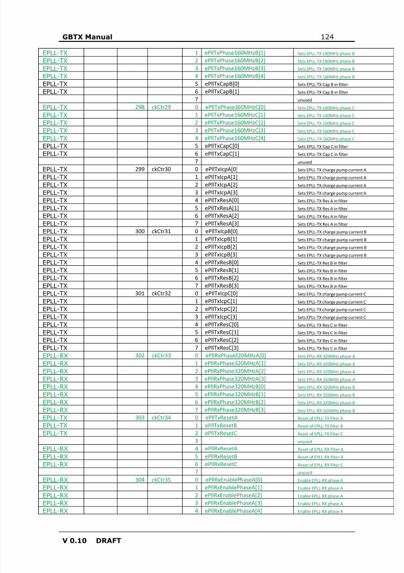
8/15/2019 gbtx Manual
http://slidepdf.com/reader/full/gbtx-manual 124/200
GBTX Manual 124
V 0.10 DRAFT
EPLL-TX 1 ePllTxPhase160MHzB[1] Sets EPLL-TX 160MHz phase B
EPLL-TX 2 ePllTxPhase160MHzB[2] Sets EPLL-TX 160MHz phase B
EPLL-TX 3 ePllTxPhase160MHzB[3] Sets EPLL-TX 160MHz phase B
EPLL-TX 4 ePllTxPhase160MHzB[4] Sets EPLL-TX 160MHz phase B
EPLL-TX 5 ePllTxCapB[0] Sets EPLL-TX Cap B in filter
EPLL-TX 6 ePllTxCapB[1] Sets EPLL-TX Cap B in filter
7 unusedEPLL-TX 298 ckCtr29 0 ePllTxPhase160MHzC[0] Sets EPLL-TX 160MHz phase C
EPLL-TX 1 ePllTxPhase160MHzC[1] Sets EPLL-TX 160MHz phase C
EPLL-TX 2 ePllTxPhase160MHzC[2] Sets EPLL-TX 160MHz phase C
EPLL-TX 3 ePllTxPhase160MHzC[3] Sets EPLL-TX 160MHz phase C
EPLL-TX 4 ePllTxPhase160MHzC[4] Sets EPLL-TX 160MHz phase C
EPLL-TX 5 ePllTxCapC[0] Sets EPLL-TX Cap C in filter
EPLL-TX 6 ePllTxCapC[1] Sets EPLL-TX Cap C in filter
7 unused
EPLL-TX 299 ckCtr30 0 ePllTxIcpA[0] Sets EPLL-TX charge pump current A
EPLL-TX 1 ePllTxIcpA[1] Sets EPLL-TX charge pump current A
EPLL-TX 2 ePllTxIcpA[2] Sets EPLL-TX charge pump current A
EPLL-TX 3 ePllTxIcpA[3] Sets EPLL-TX charge pump current A
EPLL-TX 4 ePllTxResA[0] Sets EPLL-TX Res A in filterEPLL-TX 5 ePllTxResA[1] Sets EPLL-TX Res A in filter
EPLL-TX 6 ePllTxResA[2] Sets EPLL-TX Res A in filter
EPLL-TX 7 ePllTxResA[3] Sets EPLL-TX Res A in filter
EPLL-TX 300 ckCtr31 0 ePllTxIcpB[0] Sets EPLL-TX charge pump current B
EPLL-TX 1 ePllTxIcpB[1] Sets EPLL-TX charge pump current B
EPLL-TX 2 ePllTxIcpB[2] Sets EPLL-TX charge pump current B
EPLL-TX 3 ePllTxIcpB[3] Sets EPLL-TX charge pump current B
EPLL-TX 4 ePllTxResB[0] Sets EPLL-TX Res B in filter
EPLL-TX 5 ePllTxResB[1] Sets EPLL-TX Res B in filter
EPLL-TX 6 ePllTxResB[2] Sets EPLL-TX Res B in filter
EPLL-TX 7 ePllTxResB[3] Sets EPLL-TX Res B in filter
EPLL-TX 301 ckCtr32 0 ePllTxIcpC[0] Sets EPLL-TX charge pump current C
EPLL-TX 1 ePllTxIcpC[1] Sets EPLL-TX charge pump current CEPLL-TX 2 ePllTxIcpC[2] Sets EPLL-TX charge pump current C
EPLL-TX 3 ePllTxIcpC[3] Sets EPLL-TX charge pump current C
EPLL-TX 4 ePllTxResC[0] Sets EPLL-TX Res C in filter
EPLL-TX 5 ePllTxResC[1] Sets EPLL-TX Res C in filter
EPLL-TX 6 ePllTxResC[2] Sets EPLL-TX Res C in filter
EPLL-TX 7 ePllTxResC[3] Sets EPLL-TX Res C in filter
EPLL-RX 302 ckCtr33 0 ePllRxPhase320MHzA[0] Sets EPLL-RX 320MHz phase A
EPLL-RX 1 ePllRxPhase320MHzA[1] Sets EPLL-RX 320MHz phase A
EPLL-RX 2 ePllRxPhase320MHzA[2] Sets EPLL-RX 320MHz phase A
EPLL-RX 3 ePllRxPhase320MHzA[3] Sets EPLL-RX 320MHz phase A
EPLL-RX 4 ePllRxPhase320MHzB[0] Sets EPLL-RX 320MHz phase B
EPLL-RX 5 ePllRxPhase320MHzB[1] Sets EPLL-RX 320MHz phase B
EPLL-RX 6 ePllRxPhase320MHzB[2] Sets EPLL-RX 320MHz phase B
EPLL-RX 7 ePllRxPhase320MHzB[3] Sets EPLL-RX 320MHz phase B
EPLL-TX 303 ckCtr34 0 ePllTxResetA Reset of EPLL-TX filter A
EPLL-TX 1 ePllTxResetB Reset of EPLL-TX filter B
EPLL-TX 2 ePllTxResetC Reset of EPLL-TX filter C
3 unused
EPLL-RX 4 ePllRxResetA Reset of EPLL-RX filter A
EPLL-RX 5 ePllRxResetB Reset of EPLL-RX filter B
EPLL-RX 6 ePllRxResetC Reset of EPLL-RX filter C
7 unused
EPLL-RX 304 ckCtr35 0 ePllRxEnablePhaseA[0] Enable EPLL-RX phase A
EPLL-RX 1 ePllRxEnablePhaseA[1] Enable EPLL-RX phase A
EPLL-RX 2 ePllRxEnablePhaseA[2] Enable EPLL-RX phase A
EPLL-RX 3 ePllRxEnablePhaseA[3] Enable EPLL-RX phase A
EPLL-RX 4 ePllRxEnablePhaseA[4] Enable EPLL-RX phase A
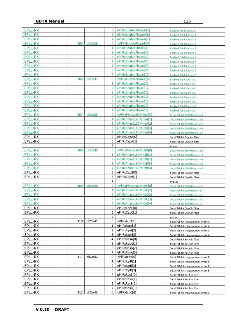
8/15/2019 gbtx Manual
http://slidepdf.com/reader/full/gbtx-manual 125/200
GBTX Manual 125
V 0.10 DRAFT
EPLL-RX 5 ePllRxEnablePhaseA[5] Enable EPLL-RX phase A
EPLL-RX 6 ePllRxEnablePhaseA[6] Enable EPLL-RX phase A
EPLL-RX 7 ePllRxEnablePhaseA[7] Enable EPLL-RX phase A
EPLL-RX 305 ckCtr36 0 ePllRxEnablePhaseB[0] Enable EPLL-RX phase B
EPLL-RX 1 ePllRxEnablePhaseB[1] Enable EPLL-RX phase B
EPLL-RX 2 ePllRxEnablePhaseB[2] Enable EPLL-RX phase B
EPLL-RX 3 ePllRxEnablePhaseB[3] Enable EPLL-RX phase BEPLL-RX 4 ePllRxEnablePhaseB[4] Enable EPLL-RX phase B
EPLL-RX 5 ePllRxEnablePhaseB[5] Enable EPLL-RX phase B
EPLL-RX 6 ePllRxEnablePhaseB[6] Enable EPLL-RX phase B
EPLL-RX 7 ePllRxEnablePhaseB[7] Enable EPLL-RX phase B
EPLL-RX 306 ckCtr37 0 ePllRxEnablePhaseC[0] Enable EPLL-RX phase C
EPLL-RX 1 ePllRxEnablePhaseC[1] Enable EPLL-RX phase C
EPLL-RX 2 ePllRxEnablePhaseC[2] Enable EPLL-RX phase C
EPLL-RX 3 ePllRxEnablePhaseC[3] Enable EPLL-RX phase C
EPLL-RX 4 ePllRxEnablePhaseC[4] Enable EPLL-RX phase C
EPLL-RX 5 ePllRxEnablePhaseC[5] Enable EPLL-RX phase C
EPLL-RX 6 ePllRxEnablePhaseC[6] Enable EPLL-RX phase C
EPLL-RX 7 ePllRxEnablePhaseC[7] Enable EPLL-RX phase C
EPLL-RX 307 ckCtr38 0 ePllRxPhase160MHzA[0] Sets EPLL-RX 160MHz phase AEPLL-RX 1 ePllRxPhase160MHzA[1] Sets EPLL-RX 160MHz phase A
EPLL-RX 2 ePllRxPhase160MHzA[2] Sets EPLL-RX 160MHz phase A
EPLL-RX 3 ePllRxPhase160MHzA[3] Sets EPLL-RX 160MHz phase A
EPLL-RX 4 ePllRxPhase160MHzA[4] Sets EPLL-RX 160MHz phase A
EPLL-RX 5 ePllRxCapA[0] Sets EPLL-RX Cap A in filter
EPLL-RX 6 ePllRxCapA[1] Sets EPLL-RX Cap A in filter
7 unused
EPLL-RX 308 ckCtr39 0 ePllRxPhase160MHzB[0] Sets EPLL-RX 160MHz phase B
EPLL-RX 1 ePllRxPhase160MHzB[1] Sets EPLL-RX 160MHz phase B
EPLL-RX 2 ePllRxPhase160MHzB[2] Sets EPLL-RX 160MHz phase B
EPLL-RX 3 ePllRxPhase160MHzB[3] Sets EPLL-RX 160MHz phase B
EPLL-RX 4 ePllRxPhase160MHzB[4] Sets EPLL-RX 160MHz phase B
EPLL-RX 5 ePllRxCapB[0] Sets EPLL-RX Cap B in filterEPLL-RX 6 ePllRxCapB[1] Sets EPLL-RX Cap B in filter
7 unused
EPLL-RX 309 ckCtr40 0 ePllRxPhase160MHzC[0] Sets EPLL-RX 160MHz phase C
EPLL-RX 1 ePllRxPhase160MHzC[1] Sets EPLL-RX 160MHz phase C
EPLL-RX 2 ePllRxPhase160MHzC[2] Sets EPLL-RX 160MHz phase C
EPLL-RX 3 ePllRxPhase160MHzC[3] Sets EPLL-RX 160MHz phase C
EPLL-RX 4 ePllRxPhase160MHzC[4] Sets EPLL-RX 160MHz phase C
EPLL-RX 5 ePllRxCapC[0] Sets EPLL-RX Cap C in filter
EPLL-RX 6 ePllRxCapC[1] Sets EPLL-RX Cap C in filter
7 unused
EPLL-RX 310 ckCtr41 0 ePllRxIcpA[0] Sets EPLL-RX charge pump current A
EPLL-RX 1 ePllRxIcpA[1] Sets EPLL-RX charge pump current A
EPLL-RX 2 ePllRxIcpA[2] Sets EPLL-RX charge pump current A
EPLL-RX 3 ePllRxIcpA[3] Sets EPLL-RX charge pump current A
EPLL-RX 4 ePllRxResA[0] Sets EPLL-RX Res A in filter
EPLL-RX 5 ePllRxResA[1] Sets EPLL-RX Res A in filter
EPLL-RX 6 ePllRxResA[2] Sets EPLL-RX Res A in filter
EPLL-RX 7 ePllRxResA[3] Sets EPLL-RX Res A in filter
EPLL-RX 311 ckCtr42 0 ePllRxIcpB[0] Sets EPLL-RX charge pump current B
EPLL-RX 1 ePllRxIcpB[1] Sets EPLL-RX charge pump current B
EPLL-RX 2 ePllRxIcpB[2] Sets EPLL-RX charge pump current B
EPLL-RX 3 ePllRxIcpB[3] Sets EPLL-RX charge pump current B
EPLL-RX 4 ePllRxResB[0] Sets EPLL-RX Res B in filter
EPLL-RX 5 ePllRxResB[1] Sets EPLL-RX Res B in filter
EPLL-RX 6 ePllRxResB[2] Sets EPLL-RX Res B in filter
EPLL-RX 7 ePllRxResB[3] Sets EPLL-RX Res B in filter
EPLL-RX 312 ckCtr43 0 ePllRxIcpC[0] Sets EPLL-RX charge pump current C
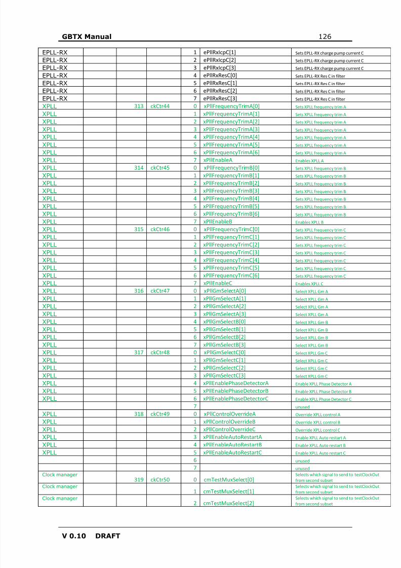
8/15/2019 gbtx Manual
http://slidepdf.com/reader/full/gbtx-manual 126/200

8/15/2019 gbtx Manual
http://slidepdf.com/reader/full/gbtx-manual 127/200
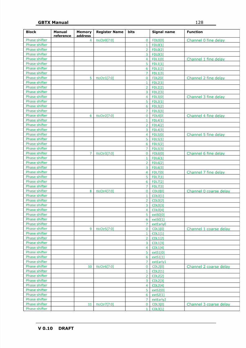
8/15/2019 gbtx Manual
http://slidepdf.com/reader/full/gbtx-manual 128/200
GBTX Manual 128
V 0.10 DRAFT
Block Manualreference
Memoryaddress
Register Name bits Signal name Function
Phase shifter 4 ttcCtr0[7:0] 0 FDL0[0] Channel 0 fine delayPhase shifter 1 FDL0[1]Phase shifter 2 FDL0[2]Phase shifter 3 FDL0[3]Phase shifter 4 FDL1[0]
Channel 1 fine delayPhase shifter 5 FDL1[1]Phase shifter 6 FDL1[2]Phase shifter 7 FDL1[3]Phase shifter 5 ttcCtr1[7:0] 0 FDL2[0] Channel 2 fine delayPhase shifter 1 FDL2[1]Phase shifter 2 FDL2[2]Phase shifter 3 FDL2[3]Phase shifter 4 FDL3[0] Channel 3 fine delayPhase shifter 5 FDL3[1]Phase shifter 6 FDL3[2]Phase shifter 7 FDL3[3]Phase shifter 6 ttcCtr2[7:0] 0 FDL4[0] Channel 4 fine delay
Phase shifter 1 FDL4[1]Phase shifter 2 FDL4[2]Phase shifter 3 FDL4[3]Phase shifter 4 FDL5[0] Channel 5 fine delayPhase shifter 5 FDL5[1]Phase shifter 6 FDL5[2]Phase shifter 7 FDL5[3]Phase shifter 7 ttcCtr3[7:0] 0 FDL6[0] Channel 6 fine delayPhase shifter 1 FDL6[1]Phase shifter 2 FDL6[2]Phase shifter 3 FDL6[3]Phase shifter 4 FDL7[0] Channel 7 fine delayPhase shifter 5 FDL7[1]
Phase shifter 6 FDL7[2]Phase shifter 7 FDL7[3]Phase shifter 8 ttcCtr4[7:0] 0 CDL0[0] Channel 0 coarse delayPhase shifter 1 CDL0[1]Phase shifter 2 CDL0[2]Phase shifter 3 CDL0[3]Phase shifter 4 CDL0[4]Phase shifter 5 extS0[0]Phase shifter 6 extS0[1]Phase shifter 7 extEarly0Phase shifter 9 ttcCtr5[7:0] 0 CDL1[0] Channel 1 coarse delayPhase shifter 1 CDL1[1]Phase shifter 2 CDL1[2]
Phase shifter 3 CDL1[3]Phase shifter 4 CDL1[4]Phase shifter 5 extS1[0]Phase shifter 6 extS1[1]Phase shifter 7 extEarly1Phase shifter 10 ttcCtr6[7:0] 0 CDL2[0] Channel 2 coarse delayPhase shifter 1 CDL2[1]Phase shifter 2 CDL2[2]Phase shifter 3 CDL2[3]Phase shifter 4 CDL2[4]Phase shifter 5 extS2[0]Phase shifter 6 extS2[1]Phase shifter 7 extEarly2
Phase shifter 11 ttcCtr7[7:0] 0 CDL3[0] Channel 3 coarse delayPhase shifter 1 CDL3[1]
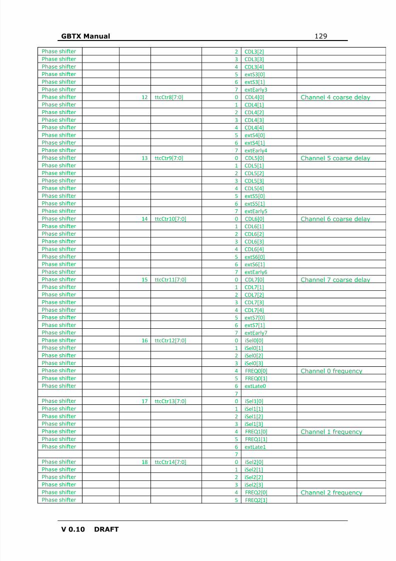
8/15/2019 gbtx Manual
http://slidepdf.com/reader/full/gbtx-manual 129/200
GBTX Manual 129
V 0.10 DRAFT
Phase shifter 2 CDL3[2]Phase shifter 3 CDL3[3]Phase shifter 4 CDL3[4]Phase shifter 5 extS3[0]Phase shifter 6 extS3[1]Phase shifter 7 extEarly3
Phase shifter 12 ttcCtr8[7:0] 0 CDL4[0] Channel 4 coarse delayPhase shifter 1 CDL4[1]Phase shifter 2 CDL4[2]Phase shifter 3 CDL4[3]Phase shifter 4 CDL4[4]Phase shifter 5 extS4[0]Phase shifter 6 extS4[1]Phase shifter 7 extEarly4Phase shifter 13 ttcCtr9[7:0] 0 CDL5[0] Channel 5 coarse delayPhase shifter 1 CDL5[1]Phase shifter 2 CDL5[2]Phase shifter 3 CDL5[3]Phase shifter 4 CDL5[4]
Phase shifter 5 extS5[0]Phase shifter 6 extS5[1]Phase shifter 7 extEarly5Phase shifter 14 ttcCtr10[7:0] 0 CDL6[0] Channel 6 coarse delayPhase shifter 1 CDL6[1]Phase shifter 2 CDL6[2]Phase shifter 3 CDL6[3]Phase shifter 4 CDL6[4]Phase shifter 5 extS6[0]Phase shifter 6 extS6[1]Phase shifter 7 extEarly6Phase shifter 15 ttcCtr11[7:0] 0 CDL7[0] Channel 7 coarse delayPhase shifter 1 CDL7[1]
Phase shifter 2 CDL7[2]Phase shifter 3 CDL7[3]Phase shifter 4 CDL7[4]Phase shifter 5 extS7[0]Phase shifter 6 extS7[1]Phase shifter 7 extEarly7Phase shifter 16 ttcCtr12[7:0] 0 iSel0[0]Phase shifter 1 iSel0[1]Phase shifter 2 iSel0[2]Phase shifter 3 iSel0[3]Phase shifter 4 FREQ0[0] Channel 0 frequencyPhase shifter 5 FREQ0[1]Phase shifter 6 extLate0
7Phase shifter 17 ttcCtr13[7:0] 0 iSel1[0]Phase shifter 1 iSel1[1]Phase shifter 2 iSel1[2]Phase shifter 3 iSel1[3]Phase shifter 4 FREQ1[0] Channel 1 frequencyPhase shifter 5 FREQ1[1]Phase shifter 6 extLate1
7Phase shifter 18 ttcCtr14[7:0] 0 iSel2[0]Phase shifter 1 iSel2[1]Phase shifter 2 iSel2[2]Phase shifter 3 iSel2[3]
Phase shifter 4 FREQ2[0] Channel 2 frequencyPhase shifter 5 FREQ2[1]
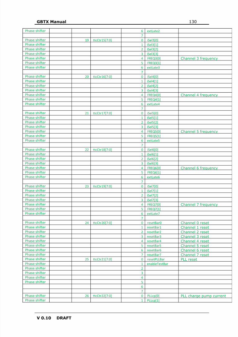
8/15/2019 gbtx Manual
http://slidepdf.com/reader/full/gbtx-manual 130/200
GBTX Manual 130
V 0.10 DRAFT
Phase shifter 6 extLate27
Phase shifter 19 ttcCtr15[7:0] 0 iSel3[0]Phase shifter 1 iSel3[1]Phase shifter 2 iSel3[2]Phase shifter 3 iSel3[3]
Phase shifter 4 FREQ3[0] Channel 3 frequencyPhase shifter 5 FREQ3[1]Phase shifter 6 extLate3
7Phase shifter 20 ttcCtr16[7:0] 0 iSel4[0]Phase shifter 1 iSel4[1]Phase shifter 2 iSel4[2]Phase shifter 3 iSel4[3]Phase shifter 4 FREQ4[0] Channel 4 frequencyPhase shifter 5 FREQ4[1]Phase shifter 6 extLate4
7Phase shifter 21 ttcCtr17[7:0] 0 iSel5[0]
Phase shifter 1 iSel5[1]Phase shifter 2 iSel5[2]Phase shifter 3 iSel5[3]Phase shifter 4 FREQ5[0] Channel 5 frequencyPhase shifter 5 FREQ5[1]Phase shifter 6 extLate5
7Phase shifter 22 ttcCtr18[7:0] 0 iSel6[0]Phase shifter 1 iSel6[1]Phase shifter 2 iSel6[2]Phase shifter 3 iSel6[3]Phase shifter 4 FREQ6[0] Channel 6 frequencyPhase shifter 5 FREQ6[1]
Phase shifter 6 extLate67
Phase shifter 23 ttcCtr19[7:0] 0 iSel7[0]Phase shifter 1 iSel7[1]Phase shifter 2 iSel7[2]Phase shifter 3 iSel7[3]Phase shifter 4 FREQ7[0] Channel 7 frequencyPhase shifter 5 FREQ7[1]Phase shifter 6 extLate7
7Phase shifter 24 ttcCtr20[7:0] 0 resetBar0 Channel 0 resetPhase shifter 1 resetBar1 Channel 1 resetPhase shifter 2 resetBar2 Channel 2 resetPhase shifter 3 resetBar3 Channel 3 resetPhase shifter 4 resetBar4 Channel 4 resetPhase shifter 5 resetBar5 Channel 5 resetPhase shifter 6 resetBar6 Channel 6 resetPhase shifter 7 resetBar7 Channel 7 resetPhase shifter 25 ttcCtr21[7:0] 0 resetPLLBar PLL resetPhase shifter 1 enableTestBarPhase shifter 2Phase shifter 3Phase shifter 4Phase shifter 5
67
Phase shifter 26 ttcCtr22[7:0] 0 PLLcp[0] PLL charge pump currentPhase shifter 1 PLLcp[1]
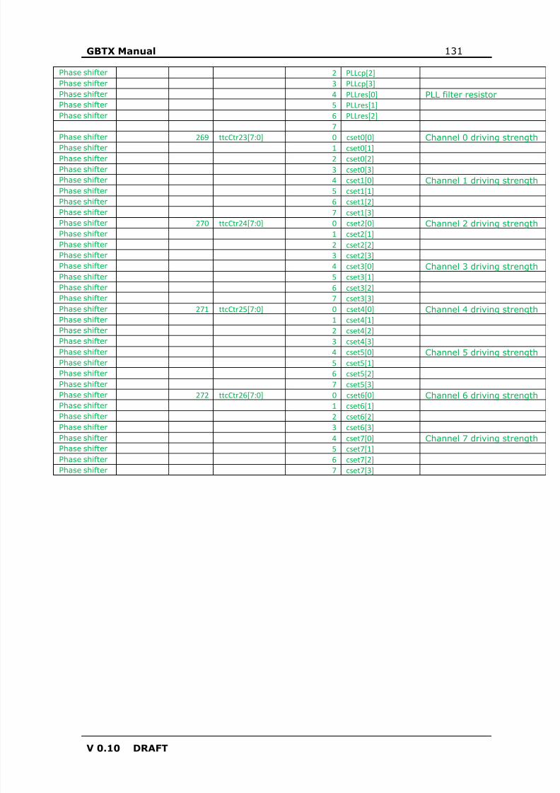
8/15/2019 gbtx Manual
http://slidepdf.com/reader/full/gbtx-manual 131/200
GBTX Manual 131
V 0.10 DRAFT
Phase shifter 2 PLLcp[2]Phase shifter 3 PLLcp[3]Phase shifter 4 PLLres[0] PLL filter resistorPhase shifter 5 PLLres[1]Phase shifter 6 PLLres[2]
7
Phase shifter 269 ttcCtr23[7:0] 0 cset0[0] Channel 0 driving strengthPhase shifter 1 cset0[1]Phase shifter 2 cset0[2]Phase shifter 3 cset0[3]Phase shifter 4 cset1[0] Channel 1 driving strengthPhase shifter 5 cset1[1]Phase shifter 6 cset1[2]Phase shifter 7 cset1[3]Phase shifter 270 ttcCtr24[7:0] 0 cset2[0] Channel 2 driving strengthPhase shifter 1 cset2[1]Phase shifter 2 cset2[2]Phase shifter 3 cset2[3]Phase shifter 4 cset3[0] Channel 3 driving strength
Phase shifter 5 cset3[1]Phase shifter 6 cset3[2]Phase shifter 7 cset3[3]Phase shifter 271 ttcCtr25[7:0] 0 cset4[0] Channel 4 driving strengthPhase shifter 1 cset4[1]Phase shifter 2 cset4[2]Phase shifter 3 cset4[3]Phase shifter 4 cset5[0] Channel 5 driving strengthPhase shifter 5 cset5[1]Phase shifter 6 cset5[2]Phase shifter 7 cset5[3]Phase shifter 272 ttcCtr26[7:0] 0 cset6[0] Channel 6 driving strengthPhase shifter 1 cset6[1]
Phase shifter 2 cset6[2]Phase shifter 3 cset6[3]Phase shifter 4 cset7[0] Channel 7 driving strengthPhase shifter 5 cset7[1]Phase shifter 6 cset7[2]Phase shifter 7 cset7[3]
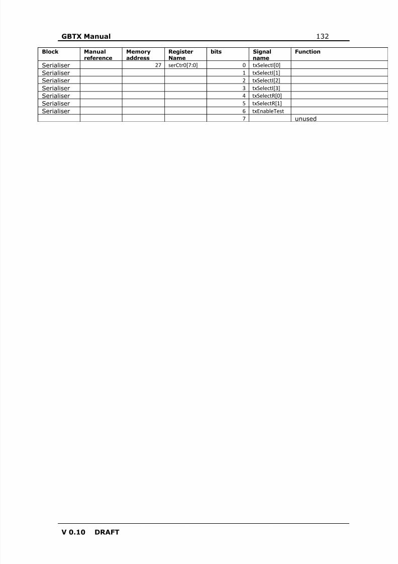
8/15/2019 gbtx Manual
http://slidepdf.com/reader/full/gbtx-manual 132/200
GBTX Manual 132
V 0.10 DRAFT
Block Manualreference
Memoryaddress
RegisterName
bits Signalname
Function
Serialiser 27 serCtr0[7:0] 0 txSelectI[0]Serialiser 1 txSelectI[1]Serialiser 2 txSelectI[2]Serialiser 3 txSelectI[3]
Serialiser4 txSelectR[0]
Serialiser 5 txSelectR[1]Serialiser 6 txEnableTest
7 unused
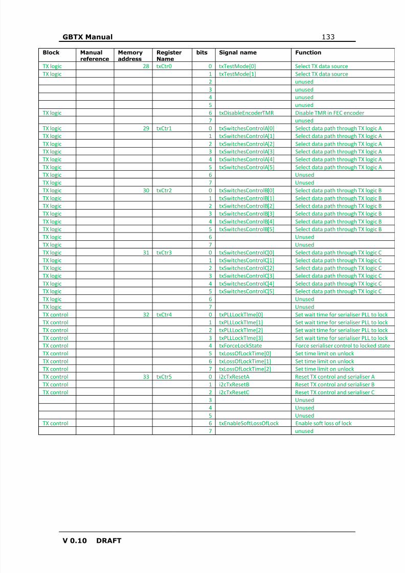
8/15/2019 gbtx Manual
http://slidepdf.com/reader/full/gbtx-manual 133/200
GBTX Manual 133
V 0.10 DRAFT
Block Manualreference
Memoryaddress
RegisterName
bits Signal name Function
TX logic 28 txCtr0 0 txTestMode[0] Select TX data sourceTX logic 1 txTestMode[1] Select TX data source
2 unused3 unused4 unused5 unused
TX logic 6 txDisableEncoderTMR Disable TMR in FEC encoder7 unused
TX logic 29 txCtr1 0 txSwitchesControlA[0] Select data path through TX logic ATX logic 1 txSwitchesControlA[1] Select data path through TX logic ATX logic 2 txSwitchesControlA[2] Select data path through TX logic ATX logic 3 txSwitchesControlA[3] Select data path through TX logic ATX logic 4 txSwitchesControlA[4] Select data path through TX logic ATX logic 5 txSwitchesControlA[5] Select data path through TX logic ATX logic 6 UnusedTX logic 7 UnusedTX logic 30 txCtr2 0 txSwitchesControlB[0] Select data path through TX logic B
TX logic 1 txSwitchesControlB[1] Select data path through TX logic BTX logic 2 txSwitchesControlB[2] Select data path through TX logic BTX logic 3 txSwitchesControlB[3] Select data path through TX logic BTX logic 4 txSwitchesControlB[4] Select data path through TX logic BTX logic 5 txSwitchesControlB[5] Select data path through TX logic BTX logic 6 UnusedTX logic 7 UnusedTX logic 31 txCtr3 0 txSwitchesControlC[0] Select data path through TX logic CTX logic 1 txSwitchesControlC[1] Select data path through TX logic CTX logic 2 txSwitchesControlC[2] Select data path through TX logic CTX logic 3 txSwitchesControlC[3] Select data path through TX logic CTX logic 4 txSwitchesControlC[4] Select data path through TX logic CTX logic 5 txSwitchesControlC[5] Select data path through TX logic C
TX logic 6 UnusedTX logic 7 UnusedTX control 32 txCtr4 0 txPLLLockTIme[0] Set wait time for serialiser PLL to lockTX control 1 txPLLLockTIme[1] Set wait time for serialiser PLL to lockTX control 2 txPLLLockTIme[2] Set wait time for serialiser PLL to lockTX control 3 txPLLLockTIme[3] Set wait time for serialiser PLL to lockTX control 4 txForceLockState Force serialiser control to locked stateTX control 5 txLossOfLockTime[0] Set time limit on unlockTX control 6 txLossOfLockTime[1] Set time limit on unlockTX control 7 txLossOfLockTime[2] Set time limit on unlockTX control 33 txCtr5 0 i2cTxResetA Reset TX control and serialiser ATX control 1 i2cTxResetB Reset TX control and serialiser BTX control 2 i2cTxResetC Reset TX control and serialiser C
3 Unused4 Unused5 Unused
TX control 6 txEnableSoftLossOfLock Enable soft loss of lock7 unused
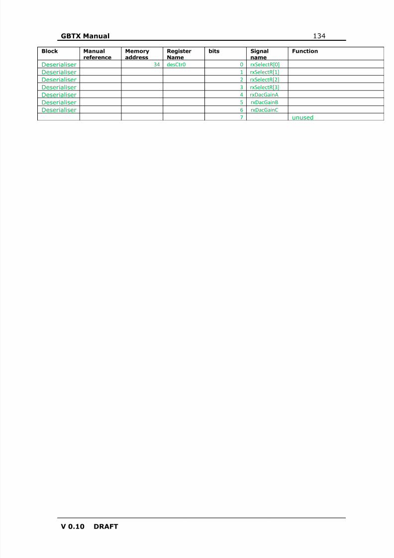
8/15/2019 gbtx Manual
http://slidepdf.com/reader/full/gbtx-manual 134/200
GBTX Manual 134
V 0.10 DRAFT
Block Manualreference
Memoryaddress
RegisterName
bits Signalname
Function
Deserialiser 34 desCtr0 0 rxSelectR[0]Deserialiser 1 rxSelectR[1]Deserialiser 2 rxSelectR[2]Deserialiser 3 rxSelectR[3]
Deserialiser4 rxDacGainA
Deserialiser 5 rxDacGainBDeserialiser 6 rxDacGainC
7 unused
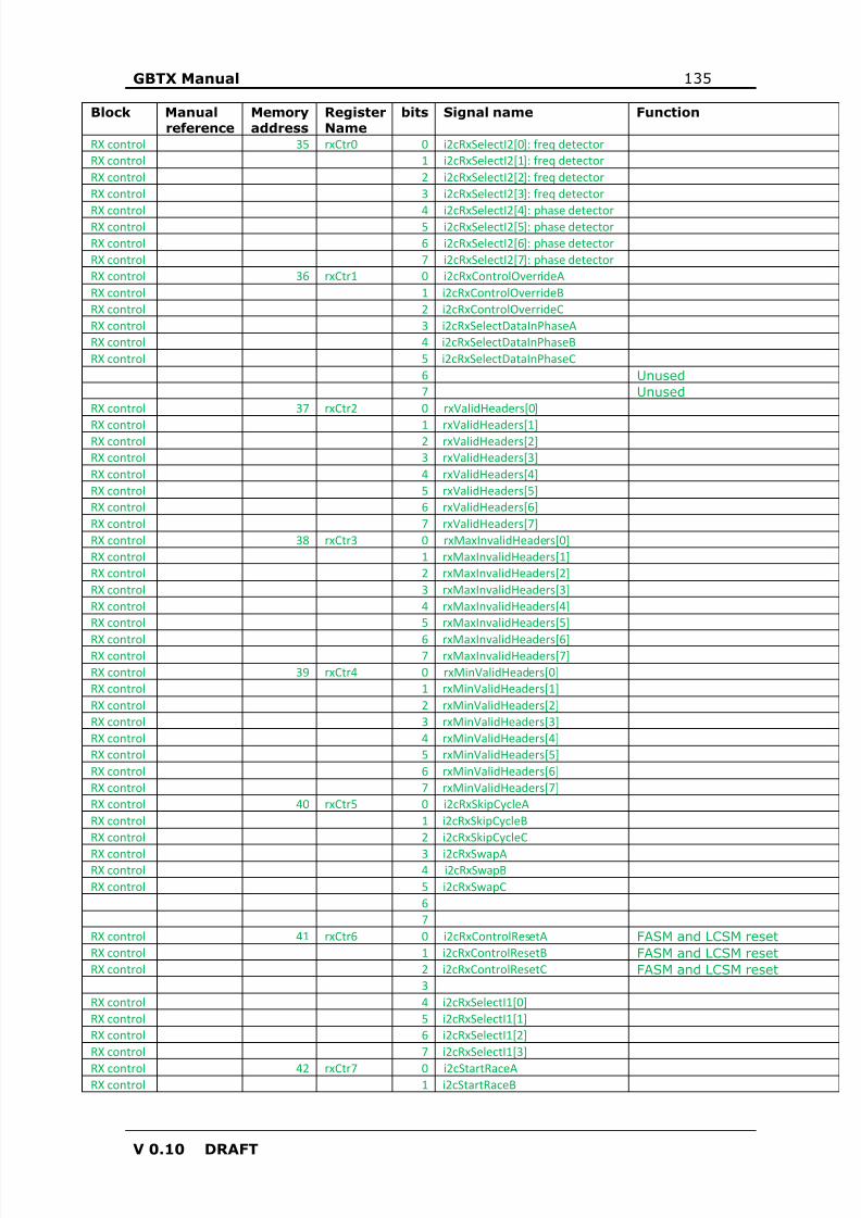
8/15/2019 gbtx Manual
http://slidepdf.com/reader/full/gbtx-manual 135/200
GBTX Manual 135
V 0.10 DRAFT
Block Manualreference
Memoryaddress
RegisterName
bits Signal name Function
RX control 35 rxCtr0 0 i2cRxSelectI2[0]: freq detectorRX control 1 i2cRxSelectI2[1]: freq detectorRX control 2 i2cRxSelectI2[2]: freq detectorRX control 3 i2cRxSelectI2[3]: freq detector
RX control 4 i2cRxSelectI2[4]: phase detectorRX control 5 i2cRxSelectI2[5]: phase detectorRX control 6 i2cRxSelectI2[6]: phase detectorRX control 7 i2cRxSelectI2[7]: phase detectorRX control 36 rxCtr1 0 i2cRxControlOverrideARX control 1 i2cRxControlOverrideBRX control 2 i2cRxControlOverrideCRX control 3 i2cRxSelectDataInPhaseARX control 4 i2cRxSelectDataInPhaseBRX control 5 i2cRxSelectDataInPhaseC
6 Unused7 Unused
RX control 37 rxCtr2 0 rxValidHeaders[0]
RX control 1 rxValidHeaders[1]RX control 2 rxValidHeaders[2]RX control 3 rxValidHeaders[3]RX control 4 rxValidHeaders[4]RX control 5 rxValidHeaders[5]RX control 6 rxValidHeaders[6]RX control 7 rxValidHeaders[7]RX control 38 rxCtr3 0 rxMaxInvalidHeaders[0]RX control 1 rxMaxInvalidHeaders[1]RX control 2 rxMaxInvalidHeaders[2]RX control 3 rxMaxInvalidHeaders[3]RX control 4 rxMaxInvalidHeaders[4]RX control 5 rxMaxInvalidHeaders[5]
RX control 6 rxMaxInvalidHeaders[6]RX control 7 rxMaxInvalidHeaders[7]RX control 39 rxCtr4 0 rxMinValidHeaders[0]RX control 1 rxMinValidHeaders[1]RX control 2 rxMinValidHeaders[2]RX control 3 rxMinValidHeaders[3]RX control 4 rxMinValidHeaders[4]RX control 5 rxMinValidHeaders[5]RX control 6 rxMinValidHeaders[6]RX control 7 rxMinValidHeaders[7]RX control 40 rxCtr5 0 i2cRxSkipCycleARX control 1 i2cRxSkipCycleBRX control 2 i2cRxSkipCycleC
RX control 3 i2cRxSwapARX control 4 i2cRxSwapBRX control 5 i2cRxSwapC
67
RX control 41 rxCtr6 0 i2cRxControlResetA FASM and LCSM resetRX control 1 i2cRxControlResetB FASM and LCSM resetRX control 2 i2cRxControlResetC FASM and LCSM reset
3RX control 4 i2cRxSelectI1[0]RX control 5 i2cRxSelectI1[1]RX control 6 i2cRxSelectI1[2]RX control 7 i2cRxSelectI1[3]
RX control 42 rxCtr7 0 i2cStartRaceARX control 1 i2cStartRaceB
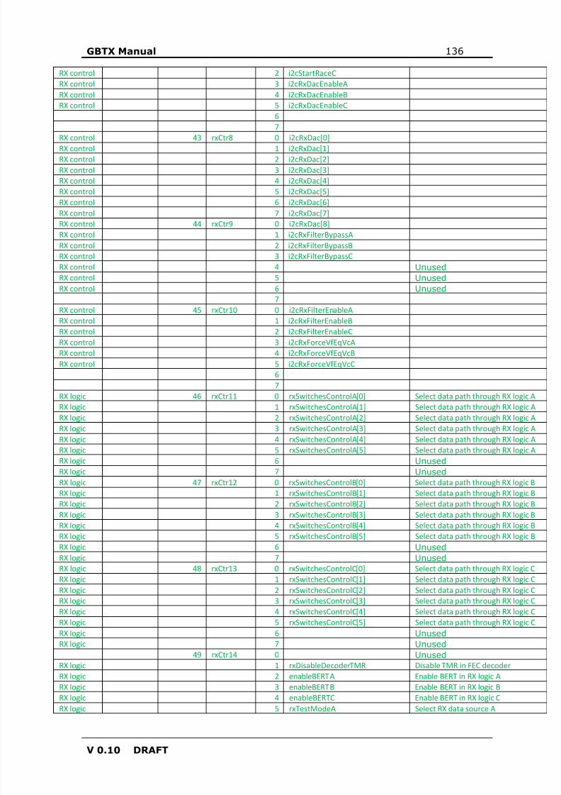
8/15/2019 gbtx Manual
http://slidepdf.com/reader/full/gbtx-manual 136/200
GBTX Manual 136
V 0.10 DRAFT
RX control 2 i2cStartRaceCRX control 3 i2cRxDacEnableARX control 4 i2cRxDacEnableBRX control 5 i2cRxDacEnableC
67
RX control 43 rxCtr8 0 i2cRxDac[0]RX control 1 i2cRxDac[1]RX control 2 i2cRxDac[2]RX control 3 i2cRxDac[3]RX control 4 i2cRxDac[4]RX control 5 i2cRxDac[5]RX control 6 i2cRxDac[6]RX control 7 i2cRxDac[7]RX control 44 rxCtr9 0 i2cRxDac[8]RX control 1 i2cRxFilterBypassARX control 2 i2cRxFilterBypassBRX control 3 i2cRxFilterBypassCRX control 4 Unused
RX control 5 UnusedRX control 6 Unused
7RX control 45 rxCtr10 0 i2cRxFilterEnableARX control 1 i2cRxFilterEnableBRX control 2 i2cRxFilterEnableCRX control 3 i2cRxForceVfEqVcARX control 4 i2cRxForceVfEqVcBRX control 5 i2cRxForceVfEqVcC
67
RX logic 46 rxCtr11 0 rxSwitchesControlA[0] Select data path through RX logic ARX logic 1 rxSwitchesControlA[1] Select data path through RX logic A
RX logic 2 rxSwitchesControlA[2] Select data path through RX logic ARX logic 3 rxSwitchesControlA[3] Select data path through RX logic ARX logic 4 rxSwitchesControlA[4] Select data path through RX logic ARX logic 5 rxSwitchesControlA[5] Select data path through RX logic ARX logic 6 UnusedRX logic 7 UnusedRX logic 47 rxCtr12 0 rxSwitchesControlB[0] Select data path through RX logic BRX logic 1 rxSwitchesControlB[1] Select data path through RX logic BRX logic 2 rxSwitchesControlB[2] Select data path through RX logic BRX logic 3 rxSwitchesControlB[3] Select data path through RX logic BRX logic 4 rxSwitchesControlB[4] Select data path through RX logic BRX logic 5 rxSwitchesControlB[5] Select data path through RX logic BRX logic 6 UnusedRX logic 7 UnusedRX logic 48 rxCtr13 0 rxSwitchesControlC[0] Select data path through RX logic CRX logic 1 rxSwitchesControlC[1] Select data path through RX logic CRX logic 2 rxSwitchesControlC[2] Select data path through RX logic CRX logic 3 rxSwitchesControlC[3] Select data path through RX logic CRX logic 4 rxSwitchesControlC[4] Select data path through RX logic CRX logic 5 rxSwitchesControlC[5] Select data path through RX logic CRX logic 6 UnusedRX logic 7 Unused
49 rxCtr14 0 Unused RX logic 1 rxDisableDecoderTMR Disable TMR in FEC decoderRX logic 2 enableBERTA Enable BERT in RX logic ARX logic 3 enableBERTB Enable BERT in RX logic B
RX logic 4 enableBERTC Enable BERT in RX logic CRX logic 5 rxTestModeA Select RX data source A
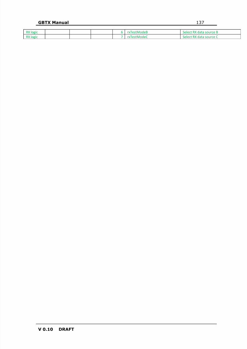
8/15/2019 gbtx Manual
http://slidepdf.com/reader/full/gbtx-manual 137/200
GBTX Manual 137
V 0.10 DRAFT
RX logic 6 rxTestModeB Select RX data source BRX logic 7 rxTestModeC Select RX data source C
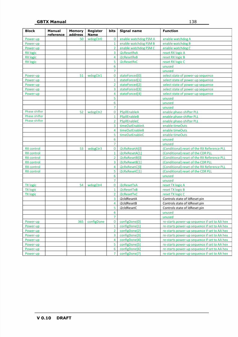
8/15/2019 gbtx Manual
http://slidepdf.com/reader/full/gbtx-manual 138/200
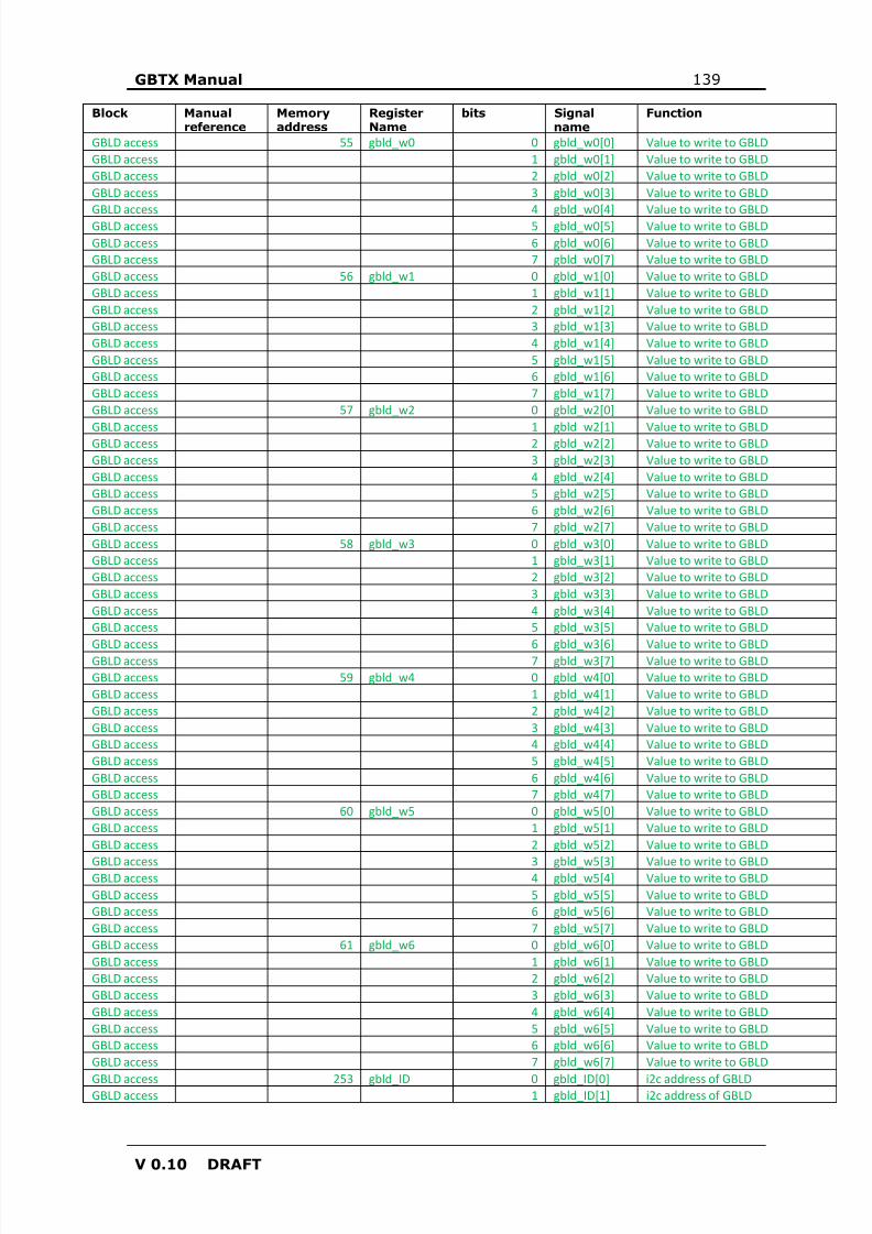
8/15/2019 gbtx Manual
http://slidepdf.com/reader/full/gbtx-manual 139/200
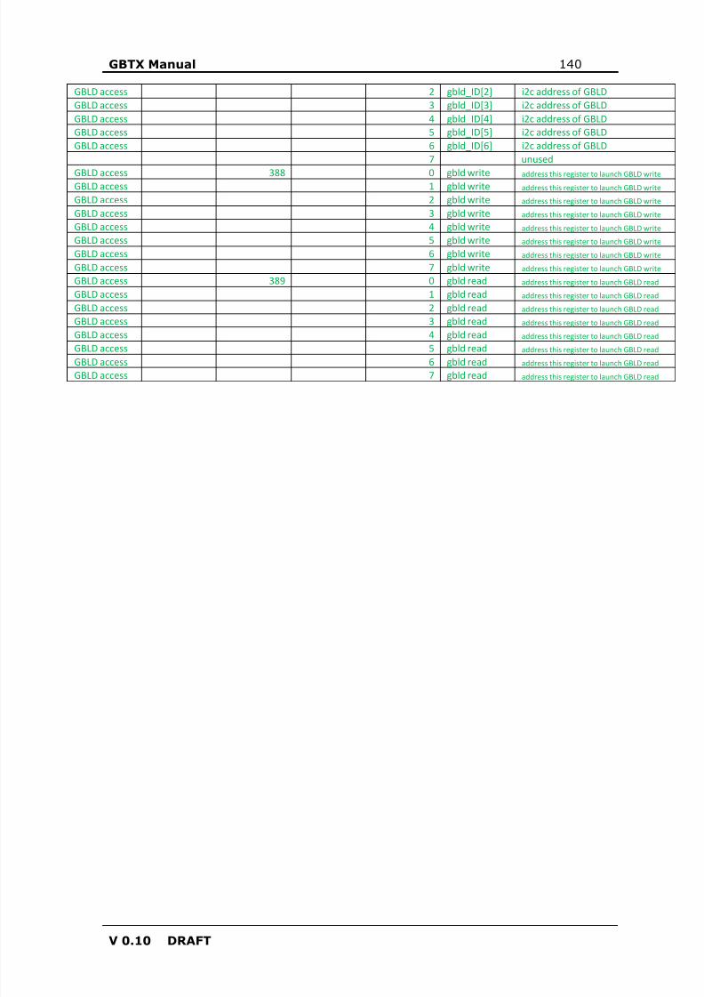
8/15/2019 gbtx Manual
http://slidepdf.com/reader/full/gbtx-manual 140/200
GBTX Manual 140
V 0.10 DRAFT
GBLD access 2 gbld_ID[2] i2c address of GBLDGBLD access 3 gbld_ID[3] i2c address of GBLDGBLD access 4 gbld_ID[4] i2c address of GBLDGBLD access 5 gbld_ID[5] i2c address of GBLDGBLD access 6 gbld_ID[6] i2c address of GBLD
7 unused
GBLD access 388 0 gbld write address this register to launch GBLD writeGBLD access 1 gbld write address this register to launch GBLD write
GBLD access 2 gbld write address this register to launch GBLD write
GBLD access 3 gbld write address this register to launch GBLD write
GBLD access 4 gbld write address this register to launch GBLD write
GBLD access 5 gbld write address this register to launch GBLD write
GBLD access 6 gbld write address this register to launch GBLD write
GBLD access 7 gbld write address this register to launch GBLD write
GBLD access 389 0 gbld read address this register to launch GBLD read
GBLD access 1 gbld read address this register to launch GBLD read
GBLD access 2 gbld read address this register to launch GBLD read
GBLD access 3 gbld read address this register to launch GBLD read
GBLD access 4 gbld read address this register to launch GBLD read
GBLD access 5 gbld read address this register to launch GBLD readGBLD access 6 gbld read address this register to launch GBLD read
GBLD access 7 gbld read address this register to launch GBLD read
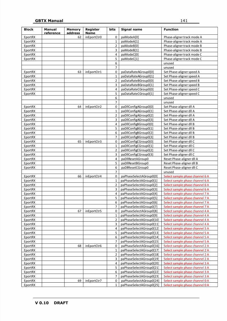
8/15/2019 gbtx Manual
http://slidepdf.com/reader/full/gbtx-manual 141/200
GBTX Manual 141
V 0.10 DRAFT
Block Manualreference
Memoryaddress
RegisterName
bits Signal name Function
EportRX 62 inEportCtr0 0 paModeA[0] Phase-aligner track mode AEportRX 1 paModeA[1] Phase-aligner track mode AEportRX 2 paModeB[0] Phase-aligner track mode BEportRX 3 paModeB[1] Phase-aligner track mode BEportRX 4 paModeC[0] Phase-aligner track mode CEportRX 5 paModeC[1] Phase-aligner track mode C
6 unused7 unused
EportRX 63 inEportCtr1 0 paDataRateAGroup0[0] Set Phase-aligner speed AEportRX 1 paDataRateAGroup0[1] Set Phase-aligner speed AEportRX 2 paDataRateBGroup0[0] Set Phase-aligner speed BEportRX 3 paDataRateBGroup0[1] Set Phase-aligner speed BEportRX 4 paDataRateCGroup0[0] Set Phase-aligner speed CEportRX 5 paDataRateCGroup0[1] Set Phase-aligner speed C
6 unused7 unused
EportRX 64 inEportCtr2 0 paDllConfigAGroup0[0] Set Phase-aligner dll A
EportRX 1 paDllConfigAGroup0[1] Set Phase-aligner dll AEportRX 2 paDllConfigAGroup0[2] Set Phase-aligner dll AEportRX 3 paDllConfigAGroup0[3] Set Phase-aligner dll AEportRX 4 paDllConfigBGroup0[0] Set Phase-aligner dll BEportRX 5 paDllConfigBGroup0[1] Set Phase-aligner dll BEportRX 6 paDllConfigBGroup0[2] Set Phase-aligner dll BEportRX 7 paDllConfigBGroup0[3] Set Phase-aligner dll BEportRX 65 inEportCtr3 0 paDllConfigCGroup0[0] Set Phase-aligner dll CEportRX 1 paDllConfigCGroup0[1] Set Phase-aligner dll CEportRX 2 paDllConfigCGroup0[2] Set Phase-aligner dll CEportRX 3 paDllConfigCGroup0[3] Set Phase-aligner dll CEportRX 4 paDllResetAGroup0 Reset Phase-aligner dll AEportRX 5 paDllResetBGroup0 Reset Phase-aligner dll B
EportRX 6 paDllResetCGroup0 Reset Phase-aligner dll C7 unusedEportRX 66 inEportCtr4 0 paPhaseSelectAGroup0[0] Select sample phase channel 6 AEportRX 1 paPhaseSelectAGroup0[1] Select sample phase channel 6 AEportRX 2 paPhaseSelectAGroup0[2] Select sample phase channel 6 AEportRX 3 paPhaseSelectAGroup0[3] Select sample phase channel 6 AEportRX 4 paPhaseSelectAGroup0[4] Select sample phase channel 7 AEportRX 5 paPhaseSelectAGroup0[5] Select sample phase channel 7 AEportRX 6 paPhaseSelectAGroup0[6] Select sample phase channel 7 AEportRX 7 paPhaseSelectAGroup0[7] Select sample phase channel 7 AEportRX 67 inEportCtr5 0 paPhaseSelectAGroup0[8] Select sample phase channel 4 AEportRX 1 paPhaseSelectAGroup0[9] Select sample phase channel 4 AEportRX 2 paPhaseSelectAGroup0[10] Select sample phase channel 4 A
EportRX 3 paPhaseSelectAGroup0[11] Select sample phase channel 4 AEportRX 4 paPhaseSelectAGroup0[12] Select sample phase channel 5 AEportRX 5 paPhaseSelectAGroup0[13] Select sample phase channel 5 AEportRX 6 paPhaseSelectAGroup0[14] Select sample phase channel 5 AEportRX 7 paPhaseSelectAGroup0[15] Select sample phase channel 5 AEportRX 68 inEportCtr6 0 paPhaseSelectAGroup0[16] Select sample phase channel 2 AEportRX 1 paPhaseSelectAGroup0[17] Select sample phase channel 2 AEportRX 2 paPhaseSelectAGroup0[18] Select sample phase channel 2 AEportRX 3 paPhaseSelectAGroup0[19] Select sample phase channel 2 AEportRX 4 paPhaseSelectAGroup0[20] Select sample phase channel 3 AEportRX 5 paPhaseSelectAGroup0[21] Select sample phase channel 3 AEportRX 6 paPhaseSelectAGroup0[22] Select sample phase channel 3 AEportRX 7 paPhaseSelectAGroup0[23] Select sample phase channel 3 A
EportRX 69 inEportCtr7 0 paPhaseSelectAGroup0[24] Select sample phase channel 0 AEportRX 1 paPhaseSelectAGroup0[25] Select sample phase channel 0 A

8/15/2019 gbtx Manual
http://slidepdf.com/reader/full/gbtx-manual 142/200
GBTX Manual 142
V 0.10 DRAFT
EportRX 2 paPhaseSelectAGroup0[26] Select sample phase channel 0 AEportRX 3 paPhaseSelectAGroup0[27] Select sample phase channel 0 AEportRX 4 paPhaseSelectAGroup0[28] Select sample phase channel 1 AEportRX 5 paPhaseSelectAGroup0[29] Select sample phase channel 1 AEportRX 6 paPhaseSelectAGroup0[30] Select sample phase channel 1 AEportRX 7 paPhaseSelectAGroup0[31] Select sample phase channel 1 A
EportRX 70 inEportCtr8 0 paPhaseSelectBGroup0[0] Select sample phase channel 6 BEportRX 1 paPhaseSelectBGroup0[1] Select sample phase channel 6 BEportRX 2 paPhaseSelectBGroup0[2] Select sample phase channel 6 BEportRX 3 paPhaseSelectBGroup0[3] Select sample phase channel 6 BEportRX 4 paPhaseSelectBGroup0[4] Select sample phase channel 7 BEportRX 5 paPhaseSelectBGroup0[5] Select sample phase channel 7 BEportRX 6 paPhaseSelectBGroup0[6] Select sample phase channel 7 BEportRX 7 paPhaseSelectBGroup0[7] Select sample phase channel 7 BEportRX 71 inEportCtr9 0 paPhaseSelectBGroup0[8] Select sample phase channel 4 BEportRX 1 paPhaseSelectBGroup0[9] Select sample phase channel 4 BEportRX 2 paPhaseSelectBGroup0[10] Select sample phase channel 4 BEportRX 3 paPhaseSelectBGroup0[11] Select sample phase channel 4 BEportRX 4 paPhaseSelectBGroup0[12] Select sample phase channel 5 B
EportRX 5 paPhaseSelectBGroup0[13] Select sample phase channel 5 BEportRX 6 paPhaseSelectBGroup0[14] Select sample phase channel 5 BEportRX 7 paPhaseSelectBGroup0[15] Select sample phase channel 5 BEportRX 72 inEportCtr10 0 paPhaseSelectBGroup0[16] Select sample phase channel 2 BEportRX 1 paPhaseSelectBGroup0[17] Select sample phase channel 2 BEportRX 2 paPhaseSelectBGroup0[18] Select sample phase channel 2 BEportRX 3 paPhaseSelectBGroup0[19] Select sample phase channel 2 BEportRX 4 paPhaseSelectBGroup0[20] Select sample phase channel 3 BEportRX 5 paPhaseSelectBGroup0[21] Select sample phase channel 3 BEportRX 6 paPhaseSelectBGroup0[22] Select sample phase channel 3 BEportRX 7 paPhaseSelectBGroup0[23] Select sample phase channel 3 BEportRX 73 inEportCtr11 0 paPhaseSelectBGroup0[24] Select sample phase channel 0 BEportRX 1 paPhaseSelectBGroup0[25] Select sample phase channel 0 B
EportRX 2 paPhaseSelectBGroup0[26] Select sample phase channel 0 BEportRX 3 paPhaseSelectBGroup0[27] Select sample phase channel 0 BEportRX 4 paPhaseSelectBGroup0[28] Select sample phase channel 1 BEportRX 5 paPhaseSelectBGroup0[29] Select sample phase channel 1 BEportRX 6 paPhaseSelectBGroup0[30] Select sample phase channel 1 BEportRX 7 paPhaseSelectBGroup0[31] Select sample phase channel 1 BEportRX 74 inEportCtr12 0 paPhaseSelectCGroup0[0] Select sample phase channel 6 CEportRX 1 paPhaseSelectCGroup0[1] Select sample phase channel 6 CEportRX 2 paPhaseSelectCGroup0[2] Select sample phase channel 6 CEportRX 3 paPhaseSelectCGroup0[3] Select sample phase channel 6 CEportRX 4 paPhaseSelectCGroup0[4] Select sample phase channel 7 CEportRX 5 paPhaseSelectCGroup0[5] Select sample phase channel 7 CEportRX 6 paPhaseSelectCGroup0[6] Select sample phase channel 7 C
EportRX 7 paPhaseSelectCGroup0[7] Select sample phase channel 7 CEportRX 75 inEportCtr13 0 paPhaseSelectCGroup0[8] Select sample phase channel 4 CEportRX 1 paPhaseSelectCGroup0[9] Select sample phase channel 4 CEportRX 2 paPhaseSelectCGroup0[10] Select sample phase channel 4 CEportRX 3 paPhaseSelectCGroup0[11] Select sample phase channel 4 CEportRX 4 paPhaseSelectCGroup0[12] Select sample phase channel 5 CEportRX 5 paPhaseSelectCGroup0[13] Select sample phase channel 5 CEportRX 6 paPhaseSelectCGroup0[14] Select sample phase channel 5 CEportRX 7 paPhaseSelectCGroup0[15] Select sample phase channel 5 CEportRX 76 inEportCtr14 0 paPhaseSelectCGroup0[16] Select sample phase channel 2 CEportRX 1 paPhaseSelectCGroup0[17] Select sample phase channel 2 CEportRX 2 paPhaseSelectCGroup0[18] Select sample phase channel 2 CEportRX 3 paPhaseSelectCGroup0[19] Select sample phase channel 2 C
EportRX 4 paPhaseSelectCGroup0[20] Select sample phase channel 3 CEportRX 5 paPhaseSelectCGroup0[21] Select sample phase channel 3 C
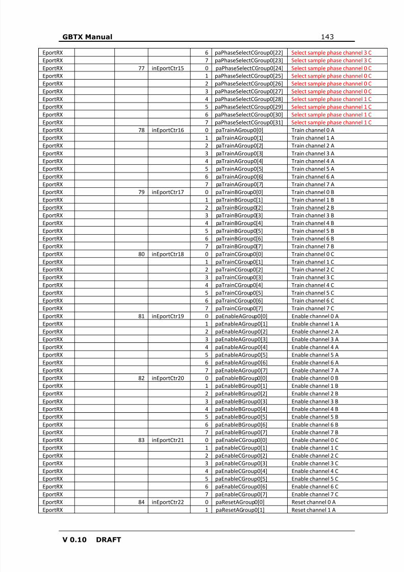
8/15/2019 gbtx Manual
http://slidepdf.com/reader/full/gbtx-manual 143/200
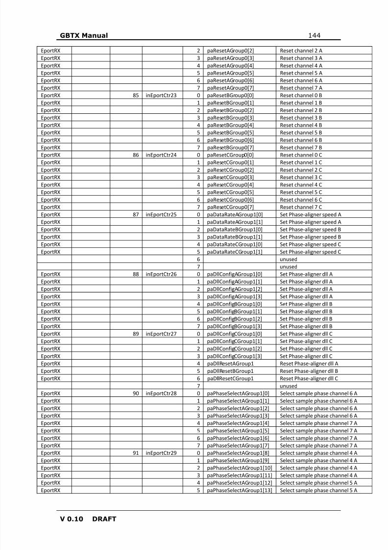
8/15/2019 gbtx Manual
http://slidepdf.com/reader/full/gbtx-manual 144/200
GBTX Manual 144
V 0.10 DRAFT
EportRX 2 paResetAGroup0[2] Reset channel 2 AEportRX 3 paResetAGroup0[3] Reset channel 3 AEportRX 4 paResetAGroup0[4] Reset channel 4 AEportRX 5 paResetAGroup0[5] Reset channel 5 AEportRX 6 paResetAGroup0[6] Reset channel 6 AEportRX 7 paResetAGroup0[7] Reset channel 7 A
EportRX 85 inEportCtr23 0 paResetBGroup0[0] Reset channel 0 BEportRX 1 paResetBGroup0[1] Reset channel 1 BEportRX 2 paResetBGroup0[2] Reset channel 2 BEportRX 3 paResetBGroup0[3] Reset channel 3 BEportRX 4 paResetBGroup0[4] Reset channel 4 BEportRX 5 paResetBGroup0[5] Reset channel 5 BEportRX 6 paResetBGroup0[6] Reset channel 6 BEportRX 7 paResetBGroup0[7] Reset channel 7 BEportRX 86 inEportCtr24 0 paResetCGroup0[0] Reset channel 0 CEportRX 1 paResetCGroup0[1] Reset channel 1 CEportRX 2 paResetCGroup0[2] Reset channel 2 CEportRX 3 paResetCGroup0[3] Reset channel 3 CEportRX 4 paResetCGroup0[4] Reset channel 4 C
EportRX 5 paResetCGroup0[5] Reset channel 5 CEportRX 6 paResetCGroup0[6] Reset channel 6 CEportRX 7 paResetCGroup0[7] Reset channel 7 CEportRX 87 inEportCtr25 0 paDataRateAGroup1[0] Set Phase-aligner speed AEportRX 1 paDataRateAGroup1[1] Set Phase-aligner speed AEportRX 2 paDataRateBGroup1[0] Set Phase-aligner speed BEportRX 3 paDataRateBGroup1[1] Set Phase-aligner speed BEportRX 4 paDataRateCGroup1[0] Set Phase-aligner speed CEportRX 5 paDataRateCGroup1[1] Set Phase-aligner speed C
6 unused7 unused
EportRX 88 inEportCtr26 0 paDllConfigAGroup1[0] Set Phase-aligner dll AEportRX 1 paDllConfigAGroup1[1] Set Phase-aligner dll A
EportRX 2 paDllConfigAGroup1[2] Set Phase-aligner dll AEportRX 3 paDllConfigAGroup1[3] Set Phase-aligner dll AEportRX 4 paDllConfigBGroup1[0] Set Phase-aligner dll BEportRX 5 paDllConfigBGroup1[1] Set Phase-aligner dll BEportRX 6 paDllConfigBGroup1[2] Set Phase-aligner dll BEportRX 7 paDllConfigBGroup1[3] Set Phase-aligner dll BEportRX 89 inEportCtr27 0 paDllConfigCGroup1[0] Set Phase-aligner dll CEportRX 1 paDllConfigCGroup1[1] Set Phase-aligner dll CEportRX 2 paDllConfigCGroup1[2] Set Phase-aligner dll CEportRX 3 paDllConfigCGroup1[3] Set Phase-aligner dll CEportRX 4 paDllResetAGroup1 Reset Phase-aligner dll AEportRX 5 paDllResetBGroup1 Reset Phase-aligner dll BEportRX 6 paDllResetCGroup1 Reset Phase-aligner dll C
7 unusedEportRX 90 inEportCtr28 0 paPhaseSelectAGroup1[0] Select sample phase channel 6 AEportRX 1 paPhaseSelectAGroup1[1] Select sample phase channel 6 AEportRX 2 paPhaseSelectAGroup1[2] Select sample phase channel 6 AEportRX 3 paPhaseSelectAGroup1[3] Select sample phase channel 6 AEportRX 4 paPhaseSelectAGroup1[4] Select sample phase channel 7 AEportRX 5 paPhaseSelectAGroup1[5] Select sample phase channel 7 AEportRX 6 paPhaseSelectAGroup1[6] Select sample phase channel 7 AEportRX 7 paPhaseSelectAGroup1[7] Select sample phase channel 7 AEportRX 91 inEportCtr29 0 paPhaseSelectAGroup1[8] Select sample phase channel 4 AEportRX 1 paPhaseSelectAGroup1[9] Select sample phase channel 4 AEportRX 2 paPhaseSelectAGroup1[10] Select sample phase channel 4 AEportRX 3 paPhaseSelectAGroup1[11] Select sample phase channel 4 A
EportRX 4 paPhaseSelectAGroup1[12] Select sample phase channel 5 AEportRX 5 paPhaseSelectAGroup1[13] Select sample phase channel 5 A

8/15/2019 gbtx Manual
http://slidepdf.com/reader/full/gbtx-manual 145/200
GBTX Manual 145
V 0.10 DRAFT
EportRX 6 paPhaseSelectAGroup1[14] Select sample phase channel 5 AEportRX 7 paPhaseSelectAGroup1[15] Select sample phase channel 5 AEportRX 92 inEportCtr30 0 paPhaseSelectAGroup1[16] Select sample phase channel 2 AEportRX 1 paPhaseSelectAGroup1[17] Select sample phase channel 2 AEportRX 2 paPhaseSelectAGroup1[18] Select sample phase channel 2 AEportRX 3 paPhaseSelectAGroup1[19] Select sample phase channel 2 A
EportRX 4 paPhaseSelectAGroup1[20] Select sample phase channel 3 AEportRX 5 paPhaseSelectAGroup1[21] Select sample phase channel 3 AEportRX 6 paPhaseSelectAGroup1[22] Select sample phase channel 3 AEportRX 7 paPhaseSelectAGroup1[23] Select sample phase channel 3 AEportRX 93 inEportCtr31 0 paPhaseSelectAGroup1[24] Select sample phase channel 0 AEportRX 1 paPhaseSelectAGroup1[25] Select sample phase channel 0 AEportRX 2 paPhaseSelectAGroup1[26] Select sample phase channel 0 AEportRX 3 paPhaseSelectAGroup1[27] Select sample phase channel 0 AEportRX 4 paPhaseSelectAGroup1[28] Select sample phase channel 1 AEportRX 5 paPhaseSelectAGroup1[29] Select sample phase channel 1 AEportRX 6 paPhaseSelectAGroup1[30] Select sample phase channel 1 AEportRX 7 paPhaseSelectAGroup1[31] Select sample phase channel 1 AEportRX 94 inEportCtr32 0 paPhaseSelectBGroup1[0] Select sample phase channel 6 B
EportRX 1 paPhaseSelectBGroup1[1] Select sample phase channel 6 BEportRX 2 paPhaseSelectBGroup1[2] Select sample phase channel 6 BEportRX 3 paPhaseSelectBGroup1[3] Select sample phase channel 6 BEportRX 4 paPhaseSelectBGroup1[4] Select sample phase channel 7 BEportRX 5 paPhaseSelectBGroup1[5] Select sample phase channel 7 BEportRX 6 paPhaseSelectBGroup1[6] Select sample phase channel 7 BEportRX 7 paPhaseSelectBGroup1[7] Select sample phase channel 7 BEportRX 95 inEportCtr33 0 paPhaseSelectBGroup1[8] Select sample phase channel 4 BEportRX 1 paPhaseSelectBGroup1[9] Select sample phase channel 4 BEportRX 2 paPhaseSelectBGroup1[10] Select sample phase channel 4 BEportRX 3 paPhaseSelectBGroup1[11] Select sample phase channel 4 BEportRX 4 paPhaseSelectBGroup1[12] Select sample phase channel 5 BEportRX 5 paPhaseSelectBGroup1[13] Select sample phase channel 5 B
EportRX 6 paPhaseSelectBGroup1[14] Select sample phase channel 5 BEportRX 7 paPhaseSelectBGroup1[15] Select sample phase channel 5 BEportRX 96 inEportCtr34 0 paPhaseSelectBGroup1[16] Select sample phase channel 2 BEportRX 1 paPhaseSelectBGroup1[17] Select sample phase channel 2 BEportRX 2 paPhaseSelectBGroup1[18] Select sample phase channel 2 BEportRX 3 paPhaseSelectBGroup1[19] Select sample phase channel 2 BEportRX 4 paPhaseSelectBGroup1[20] Select sample phase channel 3 BEportRX 5 paPhaseSelectBGroup1[21] Select sample phase channel 3 BEportRX 6 paPhaseSelectBGroup1[22] Select sample phase channel 3 BEportRX 7 paPhaseSelectBGroup1[23] Select sample phase channel 3 BEportRX 97 inEportCtr35 0 paPhaseSelectBGroup1[24] Select sample phase channel 0 BEportRX 1 paPhaseSelectBGroup1[25] Select sample phase channel 0 BEportRX 2 paPhaseSelectBGroup1[26] Select sample phase channel 0 B
EportRX 3 paPhaseSelectBGroup1[27] Select sample phase channel 0 BEportRX 4 paPhaseSelectBGroup1[28] Select sample phase channel 1 BEportRX 5 paPhaseSelectBGroup1[29] Select sample phase channel 1 BEportRX 6 paPhaseSelectBGroup1[30] Select sample phase channel 1 BEportRX 7 paPhaseSelectBGroup1[31] Select sample phase channel 1 BEportRX 98 inEportCtr36 0 paPhaseSelectCGroup1[0] Select sample phase channel 6 CEportRX 1 paPhaseSelectCGroup1[1] Select sample phase channel 6 CEportRX 2 paPhaseSelectCGroup1[2] Select sample phase channel 6 CEportRX 3 paPhaseSelectCGroup1[3] Select sample phase channel 6 CEportRX 4 paPhaseSelectCGroup1[4] Select sample phase channel 7 CEportRX 5 paPhaseSelectCGroup1[5] Select sample phase channel 7 CEportRX 6 paPhaseSelectCGroup1[6] Select sample phase channel 7 CEportRX 7 paPhaseSelectCGroup1[7] Select sample phase channel 7 C
EportRX 99 inEportCtr37 0 paPhaseSelectCGroup1[8] Select sample phase channel 4 CEportRX 1 paPhaseSelectCGroup1[9] Select sample phase channel 4 C
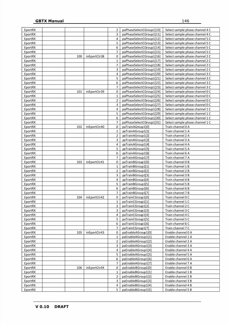
8/15/2019 gbtx Manual
http://slidepdf.com/reader/full/gbtx-manual 146/200
GBTX Manual 146
V 0.10 DRAFT
EportRX 2 paPhaseSelectCGroup1[10] Select sample phase channel 4 CEportRX 3 paPhaseSelectCGroup1[11] Select sample phase channel 4 CEportRX 4 paPhaseSelectCGroup1[12] Select sample phase channel 5 CEportRX 5 paPhaseSelectCGroup1[13] Select sample phase channel 5 CEportRX 6 paPhaseSelectCGroup1[14] Select sample phase channel 5 CEportRX 7 paPhaseSelectCGroup1[15] Select sample phase channel 5 C
EportRX 100 inEportCtr38 0 paPhaseSelectCGroup1[16] Select sample phase channel 2 CEportRX 1 paPhaseSelectCGroup1[17] Select sample phase channel 2 CEportRX 2 paPhaseSelectCGroup1[18] Select sample phase channel 2 CEportRX 3 paPhaseSelectCGroup1[19] Select sample phase channel 2 CEportRX 4 paPhaseSelectCGroup1[20] Select sample phase channel 3 CEportRX 5 paPhaseSelectCGroup1[21] Select sample phase channel 3 CEportRX 6 paPhaseSelectCGroup1[22] Select sample phase channel 3 CEportRX 7 paPhaseSelectCGroup1[23] Select sample phase channel 3 CEportRX 101 inEportCtr39 0 paPhaseSelectCGroup1[24] Select sample phase channel 0 CEportRX 1 paPhaseSelectCGroup1[25] Select sample phase channel 0 CEportRX 2 paPhaseSelectCGroup1[26] Select sample phase channel 0 CEportRX 3 paPhaseSelectCGroup1[27] Select sample phase channel 0 CEportRX 4 paPhaseSelectCGroup1[28] Select sample phase channel 1 C
EportRX 5 paPhaseSelectCGroup1[29] Select sample phase channel 1 CEportRX 6 paPhaseSelectCGroup1[30] Select sample phase channel 1 CEportRX 7 paPhaseSelectCGroup1[31] Select sample phase channel 1 CEportRX 102 inEportCtr40 0 paTrainAGroup1[0] Train channel 0 AEportRX 1 paTrainAGroup1[1] Train channel 1 AEportRX 2 paTrainAGroup1[2] Train channel 2 AEportRX 3 paTrainAGroup1[3] Train channel 3 AEportRX 4 paTrainAGroup1[4] Train channel 4 AEportRX 5 paTrainAGroup1[5] Train channel 5 AEportRX 6 paTrainAGroup1[6] Train channel 6 AEportRX 7 paTrainAGroup1[7] Train channel 7 AEportRX 103 inEportCtr41 0 paTrainBGroup1[0] Train channel 0 BEportRX 1 paTrainBGroup1[1] Train channel 1 B
EportRX 2 paTrainBGroup1[2] Train channel 2 BEportRX 3 paTrainBGroup1[3] Train channel 3 BEportRX 4 paTrainBGroup1[4] Train channel 4 BEportRX 5 paTrainBGroup1[5] Train channel 5 BEportRX 6 paTrainBGroup1[6] Train channel 6 BEportRX 7 paTrainBGroup1[7] Train channel 7 BEportRX 104 inEportCtr42 0 paTrainCGroup1[0] Train channel 0 CEportRX 1 paTrainCGroup1[1] Train channel 1 CEportRX 2 paTrainCGroup1[2] Train channel 2 CEportRX 3 paTrainCGroup1[3] Train channel 3 CEportRX 4 paTrainCGroup1[4] Train channel 4 CEportRX 5 paTrainCGroup1[5] Train channel 5 CEportRX 6 paTrainCGroup1[6] Train channel 6 C
EportRX 7 paTrainCGroup1[7] Train channel 7 CEportRX 105 inEportCtr43 0 paEnableAGroup1[0] Enable channel 0 AEportRX 1 paEnableAGroup1[1] Enable channel 1 AEportRX 2 paEnableAGroup1[2] Enable channel 2 AEportRX 3 paEnableAGroup1[3] Enable channel 3 AEportRX 4 paEnableAGroup1[4] Enable channel 4 AEportRX 5 paEnableAGroup1[5] Enable channel 5 AEportRX 6 paEnableAGroup1[6] Enable channel 6 AEportRX 7 paEnableAGroup1[7] Enable channel 7 AEportRX 106 inEportCtr44 0 paEnableBGroup1[0] Enable channel 0 BEportRX 1 paEnableBGroup1[1] Enable channel 1 BEportRX 2 paEnableBGroup1[2] Enable channel 2 BEportRX 3 paEnableBGroup1[3] Enable channel 3 B
EportRX 4 paEnableBGroup1[4] Enable channel 4 BEportRX 5 paEnableBGroup1[5] Enable channel 5 B
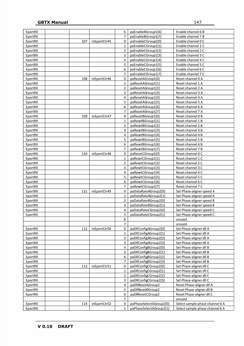
8/15/2019 gbtx Manual
http://slidepdf.com/reader/full/gbtx-manual 147/200
GBTX Manual 147
V 0.10 DRAFT
EportRX 6 paEnableBGroup1[6] Enable channel 6 BEportRX 7 paEnableBGroup1[7] Enable channel 7 BEportRX 107 inEportCtr45 0 paEnableCGroup1[0] Enable channel 0 CEportRX 1 paEnableCGroup1[1] Enable channel 1 CEportRX 2 paEnableCGroup1[2] Enable channel 2 CEportRX 3 paEnableCGroup1[3] Enable channel 3 C
EportRX 4 paEnableCGroup1[4] Enable channel 4 CEportRX 5 paEnableCGroup1[5] Enable channel 5 CEportRX 6 paEnableCGroup1[6] Enable channel 6 CEportRX 7 paEnableCGroup1[7] Enable channel 7 CEportRX 108 inEportCtr46 0 paResetAGroup1[0] Reset channel 0 AEportRX 1 paResetAGroup1[1] Reset channel 1 AEportRX 2 paResetAGroup1[2] Reset channel 2 AEportRX 3 paResetAGroup1[3] Reset channel 3 AEportRX 4 paResetAGroup1[4] Reset channel 4 AEportRX 5 paResetAGroup1[5] Reset channel 5 AEportRX 6 paResetAGroup1[6] Reset channel 6 AEportRX 7 paResetAGroup1[7] Reset channel 7 AEportRX 109 inEportCtr47 0 paResetBGroup1[0] Reset channel 0 B
EportRX 1 paResetBGroup1[1] Reset channel 1 BEportRX 2 paResetBGroup1[2] Reset channel 2 BEportRX 3 paResetBGroup1[3] Reset channel 3 BEportRX 4 paResetBGroup1[4] Reset channel 4 BEportRX 5 paResetBGroup1[5] Reset channel 5 BEportRX 6 paResetBGroup1[6] Reset channel 6 BEportRX 7 paResetBGroup1[7] Reset channel 7 BEportRX 110 inEportCtr48 0 paResetCGroup1[0] Reset channel 0 CEportRX 1 paResetCGroup1[1] Reset channel 1 CEportRX 2 paResetCGroup1[2] Reset channel 2 CEportRX 3 paResetCGroup1[3] Reset channel 3 CEportRX 4 paResetCGroup1[4] Reset channel 4 CEportRX 5 paResetCGroup1[5] Reset channel 5 C
EportRX 6 paResetCGroup1[6] Reset channel 6 CEportRX 7 paResetCGroup1[7] Reset channel 7 CEportRX 111 inEportCtr49 0 paDataRateAGroup2[0] Set Phase-aligner speed AEportRX 1 paDataRateAGroup2[1] Set Phase-aligner speed AEportRX 2 paDataRateBGroup2[0] Set Phase-aligner speed BEportRX 3 paDataRateBGroup2[1] Set Phase-aligner speed BEportRX 4 paDataRateCGroup2[0] Set Phase-aligner speed CEportRX 5 paDataRateCGroup2[1] Set Phase-aligner speed C
6 unused7 unused
EportRX 112 inEportCtr50 0 paDllConfigAGroup2[0] Set Phase-aligner dll AEportRX 1 paDllConfigAGroup2[1] Set Phase-aligner dll AEportRX 2 paDllConfigAGroup2[2] Set Phase-aligner dll A
EportRX 3 paDllConfigAGroup2[3] Set Phase-aligner dll AEportRX 4 paDllConfigBGroup2[0] Set Phase-aligner dll BEportRX 5 paDllConfigBGroup2[1] Set Phase-aligner dll BEportRX 6 paDllConfigBGroup2[2] Set Phase-aligner dll BEportRX 7 paDllConfigBGroup2[3] Set Phase-aligner dll BEportRX 113 inEportCtr51 0 paDllConfigCGroup2[0] Set Phase-aligner dll CEportRX 1 paDllConfigCGroup2[1] Set Phase-aligner dll CEportRX 2 paDllConfigCGroup2[2] Set Phase-aligner dll CEportRX 3 paDllConfigCGroup2[3] Set Phase-aligner dll CEportRX 4 paDllResetAGroup2 Reset Phase-aligner dll AEportRX 5 paDllResetBGroup2 Reset Phase-aligner dll BEportRX 6 paDllResetCGroup2 Reset Phase-aligner dll C
7 unused
EportRX 114 inEportCtr52 0 paPhaseSelectAGroup2[0] Select sample phase channel 6 AEportRX 1 paPhaseSelectAGroup2[1] Select sample phase channel 6 A
8/15/2019 gbtx Manual
http://slidepdf.com/reader/full/gbtx-manual 148/200
GBTX Manual 148
V 0.10 DRAFT
EportRX 2 paPhaseSelectAGroup2[2] Select sample phase channel 6 AEportRX 3 paPhaseSelectAGroup2[3] Select sample phase channel 6 AEportRX 4 paPhaseSelectAGroup2[4] Select sample phase channel 7 AEportRX 5 paPhaseSelectAGroup2[5] Select sample phase channel 7 AEportRX 6 paPhaseSelectAGroup2[6] Select sample phase channel 7 AEportRX 7 paPhaseSelectAGroup2[7] Select sample phase channel 7 A
EportRX 115 inEportCtr53 0 paPhaseSelectAGroup2[8] Select sample phase channel 4 AEportRX 1 paPhaseSelectAGroup2[9] Select sample phase channel 4 AEportRX 2 paPhaseSelectAGroup2[10] Select sample phase channel 4 AEportRX 3 paPhaseSelectAGroup2[11] Select sample phase channel 4 AEportRX 4 paPhaseSelectAGroup2[12] Select sample phase channel 5 AEportRX 5 paPhaseSelectAGroup2[13] Select sample phase channel 5 AEportRX 6 paPhaseSelectAGroup2[14] Select sample phase channel 5 AEportRX 7 paPhaseSelectAGroup2[15] Select sample phase channel 5 AEportRX 116 inEportCtr54 0 paPhaseSelectAGroup2[16] Select sample phase channel 2 AEportRX 1 paPhaseSelectAGroup2[17] Select sample phase channel 2 AEportRX 2 paPhaseSelectAGroup2[18] Select sample phase channel 2 AEportRX 3 paPhaseSelectAGroup2[19] Select sample phase channel 2 AEportRX 4 paPhaseSelectAGroup2[20] Select sample phase channel 3 A
EportRX 5 paPhaseSelectAGroup2[21] Select sample phase channel 3 AEportRX 6 paPhaseSelectAGroup2[22] Select sample phase channel 3 AEportRX 7 paPhaseSelectAGroup2[23] Select sample phase channel 3 AEportRX 117 inEportCtr55 0 paPhaseSelectAGroup2[24] Select sample phase channel 0 AEportRX 1 paPhaseSelectAGroup2[25] Select sample phase channel 0 AEportRX 2 paPhaseSelectAGroup2[26] Select sample phase channel 0 AEportRX 3 paPhaseSelectAGroup2[27] Select sample phase channel 0 AEportRX 4 paPhaseSelectAGroup2[28] Select sample phase channel 1 AEportRX 5 paPhaseSelectAGroup2[29] Select sample phase channel 1 AEportRX 6 paPhaseSelectAGroup2[30] Select sample phase channel 1 AEportRX 7 paPhaseSelectAGroup2[31] Select sample phase channel 1 AEportRX 118 inEportCtr56 0 paPhaseSelectBGroup2[0] Select sample phase channel 6 BEportRX 1 paPhaseSelectBGroup2[1] Select sample phase channel 6 B
EportRX 2 paPhaseSelectBGroup2[2] Select sample phase channel 6 BEportRX 3 paPhaseSelectBGroup2[3] Select sample phase channel 6 BEportRX 4 paPhaseSelectBGroup2[4] Select sample phase channel 7 BEportRX 5 paPhaseSelectBGroup2[5] Select sample phase channel 7 BEportRX 6 paPhaseSelectBGroup2[6] Select sample phase channel 7 BEportRX 7 paPhaseSelectBGroup2[7] Select sample phase channel 7 BEportRX 119 inEportCtr57 0 paPhaseSelectBGroup2[8] Select sample phase channel 4 BEportRX 1 paPhaseSelectBGroup2[9] Select sample phase channel 4 BEportRX 2 paPhaseSelectBGroup2[10] Select sample phase channel 4 BEportRX 3 paPhaseSelectBGroup2[11] Select sample phase channel 4 BEportRX 4 paPhaseSelectBGroup2[12] Select sample phase channel 5 BEportRX 5 paPhaseSelectBGroup2[13] Select sample phase channel 5 BEportRX 6 paPhaseSelectBGroup2[14] Select sample phase channel 5 B
EportRX 7 paPhaseSelectBGroup2[15] Select sample phase channel 5 BEportRX 120 inEportCtr58 0 paPhaseSelectBGroup2[16] Select sample phase channel 2 BEportRX 1 paPhaseSelectBGroup2[17] Select sample phase channel 2 BEportRX 2 paPhaseSelectBGroup2[18] Select sample phase channel 2 BEportRX 3 paPhaseSelectBGroup2[19] Select sample phase channel 2 BEportRX 4 paPhaseSelectBGroup2[20] Select sample phase channel 3 BEportRX 5 paPhaseSelectBGroup2[21] Select sample phase channel 3 BEportRX 6 paPhaseSelectBGroup2[22] Select sample phase channel 3 BEportRX 7 paPhaseSelectBGroup2[23] Select sample phase channel 3 BEportRX 121 inEportCtr59 0 paPhaseSelectBGroup2[24] Select sample phase channel 0 BEportRX 1 paPhaseSelectBGroup2[25] Select sample phase channel 0 BEportRX 2 paPhaseSelectBGroup2[26] Select sample phase channel 0 BEportRX 3 paPhaseSelectBGroup2[27] Select sample phase channel 0 B
EportRX 4 paPhaseSelectBGroup2[28] Select sample phase channel 1 BEportRX 5 paPhaseSelectBGroup2[29] Select sample phase channel 1 B
8/15/2019 gbtx Manual
http://slidepdf.com/reader/full/gbtx-manual 149/200
GBTX Manual 149
V 0.10 DRAFT
EportRX 6 paPhaseSelectBGroup2[30] Select sample phase channel 1 BEportRX 7 paPhaseSelectBGroup2[31] Select sample phase channel 1 BEportRX 122 inEportCtr60 0 paPhaseSelectCGroup2[0] Select sample phase channel 6 CEportRX 1 paPhaseSelectCGroup2[1] Select sample phase channel 6 CEportRX 2 paPhaseSelectCGroup2[2] Select sample phase channel 6 CEportRX 3 paPhaseSelectCGroup2[3] Select sample phase channel 6 C
EportRX 4 paPhaseSelectCGroup2[4] Select sample phase channel 7 CEportRX 5 paPhaseSelectCGroup2[5] Select sample phase channel 7 CEportRX 6 paPhaseSelectCGroup2[6] Select sample phase channel 7 CEportRX 7 paPhaseSelectCGroup2[7] Select sample phase channel 7 CEportRX 123 inEportCtr61 0 paPhaseSelectCGroup2[8] Select sample phase channel 4 CEportRX 1 paPhaseSelectCGroup2[9] Select sample phase channel 4 CEportRX 2 paPhaseSelectCGroup2[10] Select sample phase channel 4 CEportRX 3 paPhaseSelectCGroup2[11] Select sample phase channel 4 CEportRX 4 paPhaseSelectCGroup2[12] Select sample phase channel 5 CEportRX 5 paPhaseSelectCGroup2[13] Select sample phase channel 5 CEportRX 6 paPhaseSelectCGroup2[14] Select sample phase channel 5 CEportRX 7 paPhaseSelectCGroup2[15] Select sample phase channel 5 CEportRX 124 inEportCtr62 0 paPhaseSelectCGroup2[16] Select sample phase channel 2 C
EportRX 1 paPhaseSelectCGroup2[17] Select sample phase channel 2 CEportRX 2 paPhaseSelectCGroup2[18] Select sample phase channel 2 CEportRX 3 paPhaseSelectCGroup2[19] Select sample phase channel 2 CEportRX 4 paPhaseSelectCGroup2[20] Select sample phase channel 3 CEportRX 5 paPhaseSelectCGroup2[21] Select sample phase channel 3 CEportRX 6 paPhaseSelectCGroup2[22] Select sample phase channel 3 CEportRX 7 paPhaseSelectCGroup2[23] Select sample phase channel 3 CEportRX 125 inEportCtr63 0 paPhaseSelectCGroup2[24] Select sample phase channel 0 CEportRX 1 paPhaseSelectCGroup2[25] Select sample phase channel 0 CEportRX 2 paPhaseSelectCGroup2[26] Select sample phase channel 0 CEportRX 3 paPhaseSelectCGroup2[27] Select sample phase channel 0 CEportRX 4 paPhaseSelectCGroup2[28] Select sample phase channel 1 CEportRX 5 paPhaseSelectCGroup2[29] Select sample phase channel 1 C
EportRX 6 paPhaseSelectCGroup2[30] Select sample phase channel 1 CEportRX 7 paPhaseSelectCGroup2[31] Select sample phase channel 1 CEportRX 126 inEportCtr64 0 paTrainAGroup2[0] Train channel 0 AEportRX 1 paTrainAGroup2[1] Train channel 1 AEportRX 2 paTrainAGroup2[2] Train channel 2 AEportRX 3 paTrainAGroup2[3] Train channel 3 AEportRX 4 paTrainAGroup2[4] Train channel 4 AEportRX 5 paTrainAGroup2[5] Train channel 5 AEportRX 6 paTrainAGroup2[6] Train channel 6 AEportRX 7 paTrainAGroup2[7] Train channel 7 AEportRX 127 inEportCtr65 0 paTrainBGroup2[0] Train channel 0 BEportRX 1 paTrainBGroup2[1] Train channel 1 BEportRX 2 paTrainBGroup2[2] Train channel 2 B
EportRX 3 paTrainBGroup2[3] Train channel 3 BEportRX 4 paTrainBGroup2[4] Train channel 4 BEportRX 5 paTrainBGroup2[5] Train channel 5 BEportRX 6 paTrainBGroup2[6] Train channel 6 BEportRX 7 paTrainBGroup2[7] Train channel 7 BEportRX 128 inEportCtr66 0 paTrainCGroup2[0] Train channel 0 CEportRX 1 paTrainCGroup2[1] Train channel 1 CEportRX 2 paTrainCGroup2[2] Train channel 2 CEportRX 3 paTrainCGroup2[3] Train channel 3 CEportRX 4 paTrainCGroup2[4] Train channel 4 CEportRX 5 paTrainCGroup2[5] Train channel 5 CEportRX 6 paTrainCGroup2[6] Train channel 6 CEportRX 7 paTrainCGroup2[7] Train channel 7 C
EportRX 129 inEportCtr67 0 paEnableAGroup2[0] Enable channel 0 AEportRX 1 paEnableAGroup2[1] Enable channel 1 A
8/15/2019 gbtx Manual
http://slidepdf.com/reader/full/gbtx-manual 150/200
GBTX Manual 150
V 0.10 DRAFT
EportRX 2 paEnableAGroup2[2] Enable channel 2 AEportRX 3 paEnableAGroup2[3] Enable channel 3 AEportRX 4 paEnableAGroup2[4] Enable channel 4 AEportRX 5 paEnableAGroup2[5] Enable channel 5 AEportRX 6 paEnableAGroup2[6] Enable channel 6 AEportRX 7 paEnableAGroup2[7] Enable channel 7 A
EportRX 130 inEportCtr68 0 paEnableBGroup2[0] Enable channel 0 BEportRX 1 paEnableBGroup2[1] Enable channel 1 BEportRX 2 paEnableBGroup2[2] Enable channel 2 BEportRX 3 paEnableBGroup2[3] Enable channel 3 BEportRX 4 paEnableBGroup2[4] Enable channel 4 BEportRX 5 paEnableBGroup2[5] Enable channel 5 BEportRX 6 paEnableBGroup2[6] Enable channel 6 BEportRX 7 paEnableBGroup2[7] Enable channel 7 BEportRX 131 inEportCtr69 0 paEnableCGroup2[0] Enable channel 0 CEportRX 1 paEnableCGroup2[1] Enable channel 1 CEportRX 2 paEnableCGroup2[2] Enable channel 2 CEportRX 3 paEnableCGroup2[3] Enable channel 3 CEportRX 4 paEnableCGroup2[4] Enable channel 4 C
EportRX 5 paEnableCGroup2[5] Enable channel 5 CEportRX 6 paEnableCGroup2[6] Enable channel 6 CEportRX 7 paEnableCGroup2[7] Enable channel 7 CEportRX 132 inEportCtr70 0 paResetAGroup2[0] Reset channel 0 AEportRX 1 paResetAGroup2[1] Reset channel 1 AEportRX 2 paResetAGroup2[2] Reset channel 2 AEportRX 3 paResetAGroup2[3] Reset channel 3 AEportRX 4 paResetAGroup2[4] Reset channel 4 AEportRX 5 paResetAGroup2[5] Reset channel 5 AEportRX 6 paResetAGroup2[6] Reset channel 6 AEportRX 7 paResetAGroup2[7] Reset channel 7 AEportRX 133 inEportCtr71 0 paResetBGroup2[0] Reset channel 0 BEportRX 1 paResetBGroup2[1] Reset channel 1 B
EportRX 2 paResetBGroup2[2] Reset channel 2 BEportRX 3 paResetBGroup2[3] Reset channel 3 BEportRX 4 paResetBGroup2[4] Reset channel 4 BEportRX 5 paResetBGroup2[5] Reset channel 5 BEportRX 6 paResetBGroup2[6] Reset channel 6 BEportRX 7 paResetBGroup2[7] Reset channel 7 BEportRX 134 inEportCtr72 0 paResetCGroup2[0] Reset channel 0 CEportRX 1 paResetCGroup2[1] Reset channel 1 CEportRX 2 paResetCGroup2[2] Reset channel 2 CEportRX 3 paResetCGroup2[3] Reset channel 3 CEportRX 4 paResetCGroup2[4] Reset channel 4 CEportRX 5 paResetCGroup2[5] Reset channel 5 CEportRX 6 paResetCGroup2[6] Reset channel 6 C
EportRX 7 paResetCGroup2[7] Reset channel 7 CEportRX 135 inEportCtr73 0 paDataRateAGroup3[0] Set Phase-aligner speed AEportRX 1 paDataRateAGroup3[1] Set Phase-aligner speed AEportRX 2 paDataRateBGroup3[0] Set Phase-aligner speed BEportRX 3 paDataRateBGroup3[1] Set Phase-aligner speed BEportRX 4 paDataRateCGroup3[0] Set Phase-aligner speed CEportRX 5 paDataRateCGroup3[1] Set Phase-aligner speed C
6 unused7 unused
EportRX 136 inEportCtr74 0 paDllConfigAGroup3[0] Set Phase-aligner dll AEportRX 1 paDllConfigAGroup3[1] Set Phase-aligner dll AEportRX 2 paDllConfigAGroup3[2] Set Phase-aligner dll AEportRX 3 paDllConfigAGroup3[3] Set Phase-aligner dll A
EportRX 4 paDllConfigBGroup3[0] Set Phase-aligner dll BEportRX 5 paDllConfigBGroup3[1] Set Phase-aligner dll B
8/15/2019 gbtx Manual
http://slidepdf.com/reader/full/gbtx-manual 151/200
GBTX Manual 151
V 0.10 DRAFT
EportRX 6 paDllConfigBGroup3[2] Set Phase-aligner dll BEportRX 7 paDllConfigBGroup3[3] Set Phase-aligner dll BEportRX 137 inEportCtr75 0 paDllConfigCGroup3[0] Set Phase-aligner dll CEportRX 1 paDllConfigCGroup3[1] Set Phase-aligner dll CEportRX 2 paDllConfigCGroup3[2] Set Phase-aligner dll CEportRX 3 paDllConfigCGroup3[3] Set Phase-aligner dll C
EportRX 4 paDllResetAGroup3 Reset Phase-aligner dll AEportRX 5 paDllResetBGroup3 Reset Phase-aligner dll BEportRX 6 paDllResetCGroup3 Reset Phase-aligner dll C
7 unusedEportRX 138 inEportCtr76 0 paPhaseSelectAGroup3[0] Select sample phase channel 6 AEportRX 1 paPhaseSelectAGroup3[1] Select sample phase channel 6 AEportRX 2 paPhaseSelectAGroup3[2] Select sample phase channel 6 AEportRX 3 paPhaseSelectAGroup3[3] Select sample phase channel 6 AEportRX 4 paPhaseSelectAGroup3[4] Select sample phase channel 7 AEportRX 5 paPhaseSelectAGroup3[5] Select sample phase channel 7 AEportRX 6 paPhaseSelectAGroup3[6] Select sample phase channel 7 AEportRX 7 paPhaseSelectAGroup3[7] Select sample phase channel 7 AEportRX 139 inEportCtr77 0 paPhaseSelectAGroup3[8] Select sample phase channel 4 A
EportRX 1 paPhaseSelectAGroup3[9] Select sample phase channel 4 AEportRX 2 paPhaseSelectAGroup3[10] Select sample phase channel 4 AEportRX 3 paPhaseSelectAGroup3[11] Select sample phase channel 4 AEportRX 4 paPhaseSelectAGroup3[12] Select sample phase channel 5 AEportRX 5 paPhaseSelectAGroup3[13] Select sample phase channel 5 AEportRX 6 paPhaseSelectAGroup3[14] Select sample phase channel 5 AEportRX 7 paPhaseSelectAGroup3[15] Select sample phase channel 5 AEportRX 140 inEportCtr78 0 paPhaseSelectAGroup3[16] Select sample phase channel 2 AEportRX 1 paPhaseSelectAGroup3[17] Select sample phase channel 2 AEportRX 2 paPhaseSelectAGroup3[18] Select sample phase channel 2 AEportRX 3 paPhaseSelectAGroup3[19] Select sample phase channel 2 AEportRX 4 paPhaseSelectAGroup3[20] Select sample phase channel 3 AEportRX 5 paPhaseSelectAGroup3[21] Select sample phase channel 3 A
EportRX 6 paPhaseSelectAGroup3[22] Select sample phase channel 3 AEportRX 7 paPhaseSelectAGroup3[23] Select sample phase channel 3 AEportRX 141 inEportCtr79 0 paPhaseSelectAGroup3[24] Select sample phase channel 0 AEportRX 1 paPhaseSelectAGroup3[25] Select sample phase channel 0 AEportRX 2 paPhaseSelectAGroup3[26] Select sample phase channel 0 AEportRX 3 paPhaseSelectAGroup3[27] Select sample phase channel 0 AEportRX 4 paPhaseSelectAGroup3[28] Select sample phase channel 1 AEportRX 5 paPhaseSelectAGroup3[29] Select sample phase channel 1 AEportRX 6 paPhaseSelectAGroup3[30] Select sample phase channel 1 AEportRX 7 paPhaseSelectAGroup3[31] Select sample phase channel 1 AEportRX 142 inEportCtr80 0 paPhaseSelectBGroup3[0] Select sample phase channel 6 BEportRX 1 paPhaseSelectBGroup3[1] Select sample phase channel 6 BEportRX 2 paPhaseSelectBGroup3[2] Select sample phase channel 6 B
EportRX 3 paPhaseSelectBGroup3[3] Select sample phase channel 6 BEportRX 4 paPhaseSelectBGroup3[4] Select sample phase channel 7 BEportRX 5 paPhaseSelectBGroup3[5] Select sample phase channel 7 BEportRX 6 paPhaseSelectBGroup3[6] Select sample phase channel 7 BEportRX 7 paPhaseSelectBGroup3[7] Select sample phase channel 7 BEportRX 143 inEportCtr81 0 paPhaseSelectBGroup3[8] Select sample phase channel 4 BEportRX 1 paPhaseSelectBGroup3[9] Select sample phase channel 4 BEportRX 2 paPhaseSelectBGroup3[10] Select sample phase channel 4 BEportRX 3 paPhaseSelectBGroup3[11] Select sample phase channel 4 BEportRX 4 paPhaseSelectBGroup3[12] Select sample phase channel 5 BEportRX 5 paPhaseSelectBGroup3[13] Select sample phase channel 5 BEportRX 6 paPhaseSelectBGroup3[14] Select sample phase channel 5 BEportRX 7 paPhaseSelectBGroup3[15] Select sample phase channel 5 B
EportRX 144 inEportCtr82 0 paPhaseSelectBGroup3[16] Select sample phase channel 2 BEportRX 1 paPhaseSelectBGroup3[17] Select sample phase channel 2 B
8/15/2019 gbtx Manual
http://slidepdf.com/reader/full/gbtx-manual 152/200
GBTX Manual 152
V 0.10 DRAFT
EportRX 2 paPhaseSelectBGroup3[18] Select sample phase channel 2 BEportRX 3 paPhaseSelectBGroup3[19] Select sample phase channel 2 BEportRX 4 paPhaseSelectBGroup3[20] Select sample phase channel 3 BEportRX 5 paPhaseSelectBGroup3[21] Select sample phase channel 3 BEportRX 6 paPhaseSelectBGroup3[22] Select sample phase channel 3 BEportRX 7 paPhaseSelectBGroup3[23] Select sample phase channel 3 B
EportRX 145 inEportCtr83 0 paPhaseSelectBGroup3[24] Select sample phase channel 0 BEportRX 1 paPhaseSelectBGroup3[25] Select sample phase channel 0 BEportRX 2 paPhaseSelectBGroup3[26] Select sample phase channel 0 BEportRX 3 paPhaseSelectBGroup3[27] Select sample phase channel 0 BEportRX 4 paPhaseSelectBGroup3[28] Select sample phase channel 1 BEportRX 5 paPhaseSelectBGroup3[29] Select sample phase channel 1 BEportRX 6 paPhaseSelectBGroup3[30] Select sample phase channel 1 BEportRX 7 paPhaseSelectBGroup3[31] Select sample phase channel 1 BEportRX 146 inEportCtr84 0 paPhaseSelectCGroup3[0] Select sample phase channel 6 CEportRX 1 paPhaseSelectCGroup3[1] Select sample phase channel 6 CEportRX 2 paPhaseSelectCGroup3[2] Select sample phase channel 6 CEportRX 3 paPhaseSelectCGroup3[3] Select sample phase channel 6 CEportRX 4 paPhaseSelectCGroup3[4] Select sample phase channel 7 C
EportRX 5 paPhaseSelectCGroup3[5] Select sample phase channel 7 CEportRX 6 paPhaseSelectCGroup3[6] Select sample phase channel 7 CEportRX 7 paPhaseSelectCGroup3[7] Select sample phase channel 7 CEportRX 147 inEportCtr85 0 paPhaseSelectCGroup3[8] Select sample phase channel 4 CEportRX 1 paPhaseSelectCGroup3[9] Select sample phase channel 4 CEportRX 2 paPhaseSelectCGroup3[10] Select sample phase channel 4 CEportRX 3 paPhaseSelectCGroup3[11] Select sample phase channel 4 CEportRX 4 paPhaseSelectCGroup3[12] Select sample phase channel 5 CEportRX 5 paPhaseSelectCGroup3[13] Select sample phase channel 5 CEportRX 6 paPhaseSelectCGroup3[14] Select sample phase channel 5 CEportRX 7 paPhaseSelectCGroup3[15] Select sample phase channel 5 CEportRX 148 inEportCtr86 0 paPhaseSelectCGroup3[16] Select sample phase channel 2 CEportRX 1 paPhaseSelectCGroup3[17] Select sample phase channel 2 C
EportRX 2 paPhaseSelectCGroup3[18] Select sample phase channel 2 CEportRX 3 paPhaseSelectCGroup3[19] Select sample phase channel 2 CEportRX 4 paPhaseSelectCGroup3[20] Select sample phase channel 3 CEportRX 5 paPhaseSelectCGroup3[21] Select sample phase channel 3 CEportRX 6 paPhaseSelectCGroup3[22] Select sample phase channel 3 CEportRX 7 paPhaseSelectCGroup3[23] Select sample phase channel 3 CEportRX 149 inEportCtr87 0 paPhaseSelectCGroup3[24] Select sample phase channel 0 CEportRX 1 paPhaseSelectCGroup3[25] Select sample phase channel 0 CEportRX 2 paPhaseSelectCGroup3[26] Select sample phase channel 0 CEportRX 3 paPhaseSelectCGroup3[27] Select sample phase channel 0 CEportRX 4 paPhaseSelectCGroup3[28] Select sample phase channel 1 CEportRX 5 paPhaseSelectCGroup3[29] Select sample phase channel 1 CEportRX 6 paPhaseSelectCGroup3[30] Select sample phase channel 1 C
EportRX 7 paPhaseSelectCGroup3[31] Select sample phase channel 1 CEportRX 150 inEportCtr88 0 paTrainAGroup3[0] Train channel 0 AEportRX 1 paTrainAGroup3[1] Train channel 1 AEportRX 2 paTrainAGroup3[2] Train channel 2 AEportRX 3 paTrainAGroup3[3] Train channel 3 AEportRX 4 paTrainAGroup3[4] Train channel 4 AEportRX 5 paTrainAGroup3[5] Train channel 5 AEportRX 6 paTrainAGroup3[6] Train channel 6 AEportRX 7 paTrainAGroup3[7] Train channel 7 AEportRX 151 inEportCtr89 0 paTrainBGroup3[0] Train channel 0 BEportRX 1 paTrainBGroup3[1] Train channel 1 BEportRX 2 paTrainBGroup3[2] Train channel 2 BEportRX 3 paTrainBGroup3[3] Train channel 3 B
EportRX 4 paTrainBGroup3[4] Train channel 4 BEportRX 5 paTrainBGroup3[5] Train channel 5 B
8/15/2019 gbtx Manual
http://slidepdf.com/reader/full/gbtx-manual 153/200
GBTX Manual 153
V 0.10 DRAFT
EportRX 6 paTrainBGroup3[6] Train channel 6 BEportRX 7 paTrainBGroup3[7] Train channel 7 BEportRX 152 inEportCtr90 0 paTrainCGroup3[0] Train channel 0 CEportRX 1 paTrainCGroup3[1] Train channel 1 CEportRX 2 paTrainCGroup3[2] Train channel 2 CEportRX 3 paTrainCGroup3[3] Train channel 3 C
EportRX 4 paTrainCGroup3[4] Train channel 4 CEportRX 5 paTrainCGroup3[5] Train channel 5 CEportRX 6 paTrainCGroup3[6] Train channel 6 CEportRX 7 paTrainCGroup3[7] Train channel 7 CEportRX 153 inEportCtr91 0 paEnableAGroup3[0] Enable channel 0 AEportRX 1 paEnableAGroup3[1] Enable channel 1 AEportRX 2 paEnableAGroup3[2] Enable channel 2 AEportRX 3 paEnableAGroup3[3] Enable channel 3 AEportRX 4 paEnableAGroup3[4] Enable channel 4 AEportRX 5 paEnableAGroup3[5] Enable channel 5 AEportRX 6 paEnableAGroup3[6] Enable channel 6 AEportRX 7 paEnableAGroup3[7] Enable channel 7 AEportRX 154 inEportCtr92 0 paEnableBGroup3[0] Enable channel 0 B
EportRX 1 paEnableBGroup3[1] Enable channel 1 BEportRX 2 paEnableBGroup3[2] Enable channel 2 BEportRX 3 paEnableBGroup3[3] Enable channel 3 BEportRX 4 paEnableBGroup3[4] Enable channel 4 BEportRX 5 paEnableBGroup3[5] Enable channel 5 BEportRX 6 paEnableBGroup3[6] Enable channel 6 BEportRX 7 paEnableBGroup3[7] Enable channel 7 BEportRX 155 inEportCtr93 0 paEnableCGroup3[0] Enable channel 0 CEportRX 1 paEnableCGroup3[1] Enable channel 1 CEportRX 2 paEnableCGroup3[2] Enable channel 2 CEportRX 3 paEnableCGroup3[3] Enable channel 3 CEportRX 4 paEnableCGroup3[4] Enable channel 4 CEportRX 5 paEnableCGroup3[5] Enable channel 5 C
EportRX 6 paEnableCGroup3[6] Enable channel 6 CEportRX 7 paEnableCGroup3[7] Enable channel 7 CEportRX 156 inEportCtr94 0 paResetAGroup3[0] Reset channel 0 AEportRX 1 paResetAGroup3[1] Reset channel 1 AEportRX 2 paResetAGroup3[2] Reset channel 2 AEportRX 3 paResetAGroup3[3] Reset channel 3 AEportRX 4 paResetAGroup3[4] Reset channel 4 AEportRX 5 paResetAGroup3[5] Reset channel 5 AEportRX 6 paResetAGroup3[6] Reset channel 6 AEportRX 7 paResetAGroup3[7] Reset channel 7 AEportRX 157 inEportCtr95 0 paResetBGroup3[0] Reset channel 0 BEportRX 1 paResetBGroup3[1] Reset channel 1 BEportRX 2 paResetBGroup3[2] Reset channel 2 B
EportRX 3 paResetBGroup3[3] Reset channel 3 BEportRX 4 paResetBGroup3[4] Reset channel 4 BEportRX 5 paResetBGroup3[5] Reset channel 5 BEportRX 6 paResetBGroup3[6] Reset channel 6 BEportRX 7 paResetBGroup3[7] Reset channel 7 BEportRX 158 inEportCtr96 0 paResetCGroup3[0] Reset channel 0 CEportRX 1 paResetCGroup3[1] Reset channel 1 CEportRX 2 paResetCGroup3[2] Reset channel 2 CEportRX 3 paResetCGroup3[3] Reset channel 3 CEportRX 4 paResetCGroup3[4] Reset channel 4 CEportRX 5 paResetCGroup3[5] Reset channel 5 CEportRX 6 paResetCGroup3[6] Reset channel 6 CEportRX 7 paResetCGroup3[7] Reset channel 7 C
EportRX 159 inEportCtr97 0 paDataRateAGroup4[0] Set Phase-aligner speed AEportRX 1 paDataRateAGroup4[1] Set Phase-aligner speed A
8/15/2019 gbtx Manual
http://slidepdf.com/reader/full/gbtx-manual 154/200
GBTX Manual 154
V 0.10 DRAFT
EportRX 2 paDataRateBGroup4[0] Set Phase-aligner speed BEportRX 3 paDataRateBGroup4[1] Set Phase-aligner speed BEportRX 4 paDataRateCGroup4[0] Set Phase-aligner speed CEportRX 5 paDataRateCGroup4[1] Set Phase-aligner speed C
6 unused7 unused
EportRX 160 inEportCtr98 0 paDllConfigAGroup4[0] Set Phase-aligner dll AEportRX 1 paDllConfigAGroup4[1] Set Phase-aligner dll AEportRX 2 paDllConfigAGroup4[2] Set Phase-aligner dll AEportRX 3 paDllConfigAGroup4[3] Set Phase-aligner dll AEportRX 4 paDllConfigBGroup4[0] Set Phase-aligner dll BEportRX 5 paDllConfigBGroup4[1] Set Phase-aligner dll BEportRX 6 paDllConfigBGroup4[2] Set Phase-aligner dll BEportRX 7 paDllConfigBGroup4[3] Set Phase-aligner dll BEportRX 161 inEportCtr99 0 paDllConfigCGroup4[0] Set Phase-aligner dll CEportRX 1 paDllConfigCGroup4[1] Set Phase-aligner dll CEportRX 2 paDllConfigCGroup4[2] Set Phase-aligner dll CEportRX 3 paDllConfigCGroup4[3] Set Phase-aligner dll CEportRX 4 paDllResetAGroup4 Reset Phase-aligner dll A
EportRX 5 paDllResetBGroup4 Reset Phase-aligner dll BEportRX 6 paDllResetCGroup4 Reset Phase-aligner dll C
7 unusedEportRX 162 inEportCtr100 0 paPhaseSelectAGroup4[0] Select sample phase channel 6 AEportRX 1 paPhaseSelectAGroup4[1] Select sample phase channel 6 AEportRX 2 paPhaseSelectAGroup4[2] Select sample phase channel 6 AEportRX 3 paPhaseSelectAGroup4[3] Select sample phase channel 6 AEportRX 4 paPhaseSelectAGroup4[4] Select sample phase channel 7 AEportRX 5 paPhaseSelectAGroup4[5] Select sample phase channel 7 AEportRX 6 paPhaseSelectAGroup4[6] Select sample phase channel 7 AEportRX 7 paPhaseSelectAGroup4[7] Select sample phase channel 7 AEportRX 163 inEportCtr101 0 paPhaseSelectAGroup4[8] Select sample phase channel 4 AEportRX 1 paPhaseSelectAGroup4[9] Select sample phase channel 4 A
EportRX 2 paPhaseSelectAGroup4[10] Select sample phase channel 4 AEportRX 3 paPhaseSelectAGroup4[11] Select sample phase channel 4 AEportRX 4 paPhaseSelectAGroup4[12] Select sample phase channel 5 AEportRX 5 paPhaseSelectAGroup4[13] Select sample phase channel 5 AEportRX 6 paPhaseSelectAGroup4[14] Select sample phase channel 5 AEportRX 7 paPhaseSelectAGroup4[15] Select sample phase channel 5 AEportRX 164 inEportCtr102 0 paPhaseSelectAGroup4[16] Select sample phase channel 2 AEportRX 1 paPhaseSelectAGroup4[17] Select sample phase channel 2 AEportRX 2 paPhaseSelectAGroup4[18] Select sample phase channel 2 AEportRX 3 paPhaseSelectAGroup4[19] Select sample phase channel 2 AEportRX 4 paPhaseSelectAGroup4[20] Select sample phase channel 3 AEportRX 5 paPhaseSelectAGroup4[21] Select sample phase channel 3 AEportRX 6 paPhaseSelectAGroup4[22] Select sample phase channel 3 A
EportRX 7 paPhaseSelectAGroup4[23] Select sample phase channel 3 AEportRX 165 inEportCtr103 0 paPhaseSelectAGroup4[24] Select sample phase channel 0 AEportRX 1 paPhaseSelectAGroup4[25] Select sample phase channel 0 AEportRX 2 paPhaseSelectAGroup4[26] Select sample phase channel 0 AEportRX 3 paPhaseSelectAGroup4[27] Select sample phase channel 0 AEportRX 4 paPhaseSelectAGroup4[28] Select sample phase channel 1 AEportRX 5 paPhaseSelectAGroup4[29] Select sample phase channel 1 AEportRX 6 paPhaseSelectAGroup4[30] Select sample phase channel 1 AEportRX 7 paPhaseSelectAGroup4[31] Select sample phase channel 1 AEportRX 166 inEportCtr104 0 paPhaseSelectBGroup4[0] Select sample phase channel 6 BEportRX 1 paPhaseSelectBGroup4[1] Select sample phase channel 6 BEportRX 2 paPhaseSelectBGroup4[2] Select sample phase channel 6 BEportRX 3 paPhaseSelectBGroup4[3] Select sample phase channel 6 B
EportRX 4 paPhaseSelectBGroup4[4] Select sample phase channel 7 BEportRX 5 paPhaseSelectBGroup4[5] Select sample phase channel 7 B
8/15/2019 gbtx Manual
http://slidepdf.com/reader/full/gbtx-manual 155/200
GBTX Manual 155
V 0.10 DRAFT
EportRX 6 paPhaseSelectBGroup4[6] Select sample phase channel 7 BEportRX 7 paPhaseSelectBGroup4[7] Select sample phase channel 7 BEportRX 167 inEportCtr105 0 paPhaseSelectBGroup4[8] Select sample phase channel 4 BEportRX 1 paPhaseSelectBGroup4[9] Select sample phase channel 4 BEportRX 2 paPhaseSelectBGroup4[10] Select sample phase channel 4 BEportRX 3 paPhaseSelectBGroup4[11] Select sample phase channel 4 B
EportRX 4 paPhaseSelectBGroup4[12] Select sample phase channel 5 BEportRX 5 paPhaseSelectBGroup4[13] Select sample phase channel 5 BEportRX 6 paPhaseSelectBGroup4[14] Select sample phase channel 5 BEportRX 7 paPhaseSelectBGroup4[15] Select sample phase channel 5 BEportRX 168 inEportCtr106 0 paPhaseSelectBGroup4[16] Select sample phase channel 2 BEportRX 1 paPhaseSelectBGroup4[17] Select sample phase channel 2 BEportRX 2 paPhaseSelectBGroup4[18] Select sample phase channel 2 BEportRX 3 paPhaseSelectBGroup4[19] Select sample phase channel 2 BEportRX 4 paPhaseSelectBGroup4[20] Select sample phase channel 3 BEportRX 5 paPhaseSelectBGroup4[21] Select sample phase channel 3 BEportRX 6 paPhaseSelectBGroup4[22] Select sample phase channel 3 BEportRX 7 paPhaseSelectBGroup4[23] Select sample phase channel 3 BEportRX 169 inEportCtr107 0 paPhaseSelectBGroup4[24] Select sample phase channel 0 B
EportRX 1 paPhaseSelectBGroup4[25] Select sample phase channel 0 BEportRX 2 paPhaseSelectBGroup4[26] Select sample phase channel 0 BEportRX 3 paPhaseSelectBGroup4[27] Select sample phase channel 0 BEportRX 4 paPhaseSelectBGroup4[28] Select sample phase channel 1 BEportRX 5 paPhaseSelectBGroup4[29] Select sample phase channel 1 BEportRX 6 paPhaseSelectBGroup4[30] Select sample phase channel 1 BEportRX 7 paPhaseSelectBGroup4[31] Select sample phase channel 1 BEportRX 170 inEportCtr108 0 paPhaseSelectCGroup4[0] Select sample phase channel 6 CEportRX 1 paPhaseSelectCGroup4[1] Select sample phase channel 6 CEportRX 2 paPhaseSelectCGroup4[2] Select sample phase channel 6 CEportRX 3 paPhaseSelectCGroup4[3] Select sample phase channel 6 CEportRX 4 paPhaseSelectCGroup4[4] Select sample phase channel 7 CEportRX 5 paPhaseSelectCGroup4[5] Select sample phase channel 7 C
EportRX 6 paPhaseSelectCGroup4[6] Select sample phase channel 7 CEportRX 7 paPhaseSelectCGroup4[7] Select sample phase channel 7 CEportRX 171 inEportCtr109 0 paPhaseSelectCGroup4[8] Select sample phase channel 4 CEportRX 1 paPhaseSelectCGroup4[9] Select sample phase channel 4 CEportRX 2 paPhaseSelectCGroup4[10] Select sample phase channel 4 CEportRX 3 paPhaseSelectCGroup4[11] Select sample phase channel 4 CEportRX 4 paPhaseSelectCGroup4[12] Select sample phase channel 5 CEportRX 5 paPhaseSelectCGroup4[13] Select sample phase channel 5 CEportRX 6 paPhaseSelectCGroup4[14] Select sample phase channel 5 CEportRX 7 paPhaseSelectCGroup4[15] Select sample phase channel 5 CEportRX 172 inEportCtr110 0 paPhaseSelectCGroup4[16] Select sample phase channel 2 CEportRX 1 paPhaseSelectCGroup4[17] Select sample phase channel 2 CEportRX 2 paPhaseSelectCGroup4[18] Select sample phase channel 2 C
EportRX 3 paPhaseSelectCGroup4[19] Select sample phase channel 2 CEportRX 4 paPhaseSelectCGroup4[20] Select sample phase channel 3 CEportRX 5 paPhaseSelectCGroup4[21] Select sample phase channel 3 CEportRX 6 paPhaseSelectCGroup4[22] Select sample phase channel 3 CEportRX 7 paPhaseSelectCGroup4[23] Select sample phase channel 3 CEportRX 173 inEportCtr111 0 paPhaseSelectCGroup4[24] Select sample phase channel 0 CEportRX 1 paPhaseSelectCGroup4[25] Select sample phase channel 0 CEportRX 2 paPhaseSelectCGroup4[26] Select sample phase channel 0 CEportRX 3 paPhaseSelectCGroup4[27] Select sample phase channel 0 CEportRX 4 paPhaseSelectCGroup4[28] Select sample phase channel 1 CEportRX 5 paPhaseSelectCGroup4[29] Select sample phase channel 1 CEportRX 6 paPhaseSelectCGroup4[30] Select sample phase channel 1 CEportRX 7 paPhaseSelectCGroup4[31] Select sample phase channel 1 C
EportRX 174 inEportCtr112 0 paTrainAGroup4[0] Train channel 0 AEportRX 1 paTrainAGroup4[1] Train channel 1 A
8/15/2019 gbtx Manual
http://slidepdf.com/reader/full/gbtx-manual 156/200
GBTX Manual 156
V 0.10 DRAFT
EportRX 2 paTrainAGroup4[2] Train channel 2 AEportRX 3 paTrainAGroup4[3] Train channel 3 AEportRX 4 paTrainAGroup4[4] Train channel 4 AEportRX 5 paTrainAGroup4[5] Train channel 5 AEportRX 6 paTrainAGroup4[6] Train channel 6 AEportRX 7 paTrainAGroup4[7] Train channel 7 A
EportRX 175 inEportCtr113 0 paTrainBGroup4[0] Train channel 0 BEportRX 1 paTrainBGroup4[1] Train channel 1 BEportRX 2 paTrainBGroup4[2] Train channel 2 BEportRX 3 paTrainBGroup4[3] Train channel 3 BEportRX 4 paTrainBGroup4[4] Train channel 4 BEportRX 5 paTrainBGroup4[5] Train channel 5 BEportRX 6 paTrainBGroup4[6] Train channel 6 BEportRX 7 paTrainBGroup4[7] Train channel 7 BEportRX 176 inEportCtr114 0 paTrainCGroup4[0] Train channel 0 CEportRX 1 paTrainCGroup4[1] Train channel 1 CEportRX 2 paTrainCGroup4[2] Train channel 2 CEportRX 3 paTrainCGroup4[3] Train channel 3 CEportRX 4 paTrainCGroup4[4] Train channel 4 C
EportRX 5 paTrainCGroup4[5] Train channel 5 CEportRX 6 paTrainCGroup4[6] Train channel 6 CEportRX 7 paTrainCGroup4[7] Train channel 7 CEportRX 177 inEportCtr115 0 paEnableAGroup4[0] Enable channel 0 AEportRX 1 paEnableAGroup4[1] Enable channel 1 AEportRX 2 paEnableAGroup4[2] Enable channel 2 AEportRX 3 paEnableAGroup4[3] Enable channel 3 AEportRX 4 paEnableAGroup4[4] Enable channel 4 AEportRX 5 paEnableAGroup4[5] Enable channel 5 AEportRX 6 paEnableAGroup4[6] Enable channel 6 AEportRX 7 paEnableAGroup4[7] Enable channel 7 AEportRX 178 inEportCtr116 0 paEnableBGroup4[0] Enable channel 0 BEportRX 1 paEnableBGroup4[1] Enable channel 1 B
EportRX 2 paEnableBGroup4[2] Enable channel 2 BEportRX 3 paEnableBGroup4[3] Enable channel 3 BEportRX 4 paEnableBGroup4[4] Enable channel 4 BEportRX 5 paEnableBGroup4[5] Enable channel 5 BEportRX 6 paEnableBGroup4[6] Enable channel 6 BEportRX 7 paEnableBGroup4[7] Enable channel 7 BEportRX 179 inEportCtr117 0 paEnableCGroup4[0] Enable channel 0 CEportRX 1 paEnableCGroup4[1] Enable channel 1 CEportRX 2 paEnableCGroup4[2] Enable channel 2 CEportRX 3 paEnableCGroup4[3] Enable channel 3 CEportRX 4 paEnableCGroup4[4] Enable channel 4 CEportRX 5 paEnableCGroup4[5] Enable channel 5 CEportRX 6 paEnableCGroup4[6] Enable channel 6 C
EportRX 7 paEnableCGroup4[7] Enable channel 7 CEportRX 180 inEportCtr118 0 paResetAGroup4[0] Reset channel 0 AEportRX 1 paResetAGroup4[1] Reset channel 1 AEportRX 2 paResetAGroup4[2] Reset channel 2 AEportRX 3 paResetAGroup4[3] Reset channel 3 AEportRX 4 paResetAGroup4[4] Reset channel 4 AEportRX 5 paResetAGroup4[5] Reset channel 5 AEportRX 6 paResetAGroup4[6] Reset channel 6 AEportRX 7 paResetAGroup4[7] Reset channel 7 AEportRX 181 inEportCtr119 0 paResetBGroup4[0] Reset channel 0 BEportRX 1 paResetBGroup4[1] Reset channel 1 BEportRX 2 paResetBGroup4[2] Reset channel 2 BEportRX 3 paResetBGroup4[3] Reset channel 3 B
EportRX 4 paResetBGroup4[4] Reset channel 4 BEportRX 5 paResetBGroup4[5] Reset channel 5 B
8/15/2019 gbtx Manual
http://slidepdf.com/reader/full/gbtx-manual 157/200
GBTX Manual 157
V 0.10 DRAFT
EportRX 6 paResetBGroup4[6] Reset channel 6 BEportRX 7 paResetBGroup4[7] Reset channel 7 BEportRX 182 inEportCtr120 0 paResetCGroup4[0] Reset channel 0 CEportRX 1 paResetCGroup4[1] Reset channel 1 CEportRX 2 paResetCGroup4[2] Reset channel 2 CEportRX 3 paResetCGroup4[3] Reset channel 3 C
EportRX 4 paResetCGroup4[4] Reset channel 4 CEportRX 5 paResetCGroup4[5] Reset channel 5 CEportRX 6 paResetCGroup4[6] Reset channel 6 CEportRX 7 paResetCGroup4[7] Reset channel 7 CEportRX 183 inEportCtr121 0 paDataRateAGroup5[0] Set Phase-aligner speed AEportRX 1 paDataRateAGroup5[1] Set Phase-aligner speed AEportRX 2 paDataRateBGroup5[0] Set Phase-aligner speed BEportRX 3 paDataRateBGroup5[1] Set Phase-aligner speed BEportRX 4 paDataRateCGroup5[0] Set Phase-aligner speed CEportRX 5 paDataRateCGroup5[1] Set Phase-aligner speed C
6 unused7 unused
EportRX 184 inEportCtr122 0 paDllConfigAGroup5[0] Set Phase-aligner dll A
EportRX 1 paDllConfigAGroup5[1] Set Phase-aligner dll AEportRX 2 paDllConfigAGroup5[2] Set Phase-aligner dll AEportRX 3 paDllConfigAGroup5[3] Set Phase-aligner dll AEportRX 4 paDllConfigBGroup5[0] Set Phase-aligner dll BEportRX 5 paDllConfigBGroup5[1] Set Phase-aligner dll BEportRX 6 paDllConfigBGroup5[2] Set Phase-aligner dll BEportRX 7 paDllConfigBGroup5[3] Set Phase-aligner dll BEportRX 185 inEportCtr123 0 paDllConfigCGroup5[0] Set Phase-aligner dll CEportRX 1 paDllConfigCGroup5[1] Set Phase-aligner dll CEportRX 2 paDllConfigCGroup5[2] Set Phase-aligner dll CEportRX 3 paDllConfigCGroup5[3] Set Phase-aligner dll CEportRX 4 paDllResetAGroup5 Reset Phase-aligner dll AEportRX 5 paDllResetBGroup5 Reset Phase-aligner dll B
EportRX 6 paDllResetCGroup5 Reset Phase-aligner dll C7 unused
EportRX 186 inEportCtr124 0 paPhaseSelectAGroup5[0] Select sample phase channel 6 AEportRX 1 paPhaseSelectAGroup5[1] Select sample phase channel 6 AEportRX 2 paPhaseSelectAGroup5[2] Select sample phase channel 6 AEportRX 3 paPhaseSelectAGroup5[3] Select sample phase channel 6 AEportRX 4 paPhaseSelectAGroup5[4] Select sample phase channel 7 AEportRX 5 paPhaseSelectAGroup5[5] Select sample phase channel 7 AEportRX 6 paPhaseSelectAGroup5[6] Select sample phase channel 7 AEportRX 7 paPhaseSelectAGroup5[7] Select sample phase channel 7 AEportRX 187 inEportCtr125 0 paPhaseSelectAGroup5[8] Select sample phase channel 4 AEportRX 1 paPhaseSelectAGroup5[9] Select sample phase channel 4 AEportRX 2 paPhaseSelectAGroup5[10] Select sample phase channel 4 A
EportRX 3 paPhaseSelectAGroup5[11] Select sample phase channel 4 AEportRX 4 paPhaseSelectAGroup5[12] Select sample phase channel 5 AEportRX 5 paPhaseSelectAGroup5[13] Select sample phase channel 5 AEportRX 6 paPhaseSelectAGroup5[14] Select sample phase channel 5 AEportRX 7 paPhaseSelectAGroup5[15] Select sample phase channel 5 AEportRX 188 inEportCtr126 0 paPhaseSelectAGroup5[16] Select sample phase channel 2 AEportRX 1 paPhaseSelectAGroup5[17] Select sample phase channel 2 AEportRX 2 paPhaseSelectAGroup5[18] Select sample phase channel 2 AEportRX 3 paPhaseSelectAGroup5[19] Select sample phase channel 2 AEportRX 4 paPhaseSelectAGroup5[20] Select sample phase channel 3 AEportRX 5 paPhaseSelectAGroup5[21] Select sample phase channel 3 AEportRX 6 paPhaseSelectAGroup5[22] Select sample phase channel 3 AEportRX 7 paPhaseSelectAGroup5[23] Select sample phase channel 3 A
EportRX 189 inEportCtr127 0 paPhaseSelectAGroup5[24] Select sample phase channel 0 AEportRX 1 paPhaseSelectAGroup5[25] Select sample phase channel 0 A
8/15/2019 gbtx Manual
http://slidepdf.com/reader/full/gbtx-manual 158/200
GBTX Manual 158
V 0.10 DRAFT
EportRX 2 paPhaseSelectAGroup5[26] Select sample phase channel 0 AEportRX 3 paPhaseSelectAGroup5[27] Select sample phase channel 0 AEportRX 4 paPhaseSelectAGroup5[28] Select sample phase channel 1 AEportRX 5 paPhaseSelectAGroup5[29] Select sample phase channel 1 AEportRX 6 paPhaseSelectAGroup5[30] Select sample phase channel 1 AEportRX 7 paPhaseSelectAGroup5[31] Select sample phase channel 1 A
EportRX 190 inEportCtr128 0 paPhaseSelectBGroup5[0] Select sample phase channel 6 BEportRX 1 paPhaseSelectBGroup5[1] Select sample phase channel 6 BEportRX 2 paPhaseSelectBGroup5[2] Select sample phase channel 6 BEportRX 3 paPhaseSelectBGroup5[3] Select sample phase channel 6 BEportRX 4 paPhaseSelectBGroup5[4] Select sample phase channel 7 BEportRX 5 paPhaseSelectBGroup5[5] Select sample phase channel 7 BEportRX 6 paPhaseSelectBGroup5[6] Select sample phase channel 7 BEportRX 7 paPhaseSelectBGroup5[7] Select sample phase channel 7 BEportRX 191 inEportCtr129 0 paPhaseSelectBGroup5[8] Select sample phase channel 4 BEportRX 1 paPhaseSelectBGroup5[9] Select sample phase channel 4 BEportRX 2 paPhaseSelectBGroup5[10] Select sample phase channel 4 BEportRX 3 paPhaseSelectBGroup5[11] Select sample phase channel 4 BEportRX 4 paPhaseSelectBGroup5[12] Select sample phase channel 5 B
EportRX 5 paPhaseSelectBGroup5[13] Select sample phase channel 5 BEportRX 6 paPhaseSelectBGroup5[14] Select sample phase channel 5 BEportRX 7 paPhaseSelectBGroup5[15] Select sample phase channel 5 BEportRX 192 inEportCtr130 0 paPhaseSelectBGroup5[16] Select sample phase channel 2 BEportRX 1 paPhaseSelectBGroup5[17] Select sample phase channel 2 BEportRX 2 paPhaseSelectBGroup5[18] Select sample phase channel 2 BEportRX 3 paPhaseSelectBGroup5[19] Select sample phase channel 2 BEportRX 4 paPhaseSelectBGroup5[20] Select sample phase channel 3 BEportRX 5 paPhaseSelectBGroup5[21] Select sample phase channel 3 BEportRX 6 paPhaseSelectBGroup5[22] Select sample phase channel 3 BEportRX 7 paPhaseSelectBGroup5[23] Select sample phase channel 3 BEportRX 193 inEportCtr131 0 paPhaseSelectBGroup5[24] Select sample phase channel 0 BEportRX 1 paPhaseSelectBGroup5[25] Select sample phase channel 0 B
EportRX 2 paPhaseSelectBGroup5[26] Select sample phase channel 0 BEportRX 3 paPhaseSelectBGroup5[27] Select sample phase channel 0 BEportRX 4 paPhaseSelectBGroup5[28] Select sample phase channel 1 BEportRX 5 paPhaseSelectBGroup5[29] Select sample phase channel 1 BEportRX 6 paPhaseSelectBGroup5[30] Select sample phase channel 1 BEportRX 7 paPhaseSelectBGroup5[31] Select sample phase channel 1 BEportRX 194 inEportCtr132 0 paPhaseSelectCGroup5[0] Select sample phase channel 6 CEportRX 1 paPhaseSelectCGroup5[1] Select sample phase channel 6 CEportRX 2 paPhaseSelectCGroup5[2] Select sample phase channel 6 CEportRX 3 paPhaseSelectCGroup5[3] Select sample phase channel 6 CEportRX 4 paPhaseSelectCGroup5[4] Select sample phase channel 7 CEportRX 5 paPhaseSelectCGroup5[5] Select sample phase channel 7 CEportRX 6 paPhaseSelectCGroup5[6] Select sample phase channel 7 C
EportRX 7 paPhaseSelectCGroup5[7] Select sample phase channel 7 CEportRX 195 inEportCtr133 0 paPhaseSelectCGroup5[8] Select sample phase channel 4 CEportRX 1 paPhaseSelectCGroup5[9] Select sample phase channel 4 CEportRX 2 paPhaseSelectCGroup5[10] Select sample phase channel 4 CEportRX 3 paPhaseSelectCGroup5[11] Select sample phase channel 4 CEportRX 4 paPhaseSelectCGroup5[12] Select sample phase channel 5 CEportRX 5 paPhaseSelectCGroup5[13] Select sample phase channel 5 CEportRX 6 paPhaseSelectCGroup5[14] Select sample phase channel 5 CEportRX 7 paPhaseSelectCGroup5[15] Select sample phase channel 5 CEportRX 196 inEportCtr134 0 paPhaseSelectCGroup5[16] Select sample phase channel 2 CEportRX 1 paPhaseSelectCGroup5[17] Select sample phase channel 2 CEportRX 2 paPhaseSelectCGroup5[18] Select sample phase channel 2 CEportRX 3 paPhaseSelectCGroup5[19] Select sample phase channel 2 C
EportRX 4 paPhaseSelectCGroup5[20] Select sample phase channel 3 CEportRX 5 paPhaseSelectCGroup5[21] Select sample phase channel 3 C
8/15/2019 gbtx Manual
http://slidepdf.com/reader/full/gbtx-manual 159/200
GBTX Manual 159
V 0.10 DRAFT
EportRX 6 paPhaseSelectCGroup5[22] Select sample phase channel 3 CEportRX 7 paPhaseSelectCGroup5[23] Select sample phase channel 3 CEportRX 197 inEportCtr135 0 paPhaseSelectCGroup5[24] Select sample phase channel 0 CEportRX 1 paPhaseSelectCGroup5[25] Select sample phase channel 0 CEportRX 2 paPhaseSelectCGroup5[26] Select sample phase channel 0 CEportRX 3 paPhaseSelectCGroup5[27] Select sample phase channel 0 C
EportRX 4 paPhaseSelectCGroup5[28] Select sample phase channel 1 CEportRX 5 paPhaseSelectCGroup5[29] Select sample phase channel 1 CEportRX 6 paPhaseSelectCGroup5[30] Select sample phase channel 1 CEportRX 7 paPhaseSelectCGroup5[31] Select sample phase channel 1 CEportRX 198 inEportCtr136 0 paTrainAGroup5[0] Train channel 0 AEportRX 1 paTrainAGroup5[1] Train channel 1 AEportRX 2 paTrainAGroup5[2] Train channel 2 AEportRX 3 paTrainAGroup5[3] Train channel 3 AEportRX 4 paTrainAGroup5[4] Train channel 4 AEportRX 5 paTrainAGroup5[5] Train channel 5 AEportRX 6 paTrainAGroup5[6] Train channel 6 AEportRX 7 paTrainAGroup5[7] Train channel 7 AEportRX 199 inEportCtr137 0 paTrainBGroup5[0] Train channel 0 B
EportRX 1 paTrainBGroup5[1] Train channel 1 BEportRX 2 paTrainBGroup5[2] Train channel 2 BEportRX 3 paTrainBGroup5[3] Train channel 3 BEportRX 4 paTrainBGroup5[4] Train channel 4 BEportRX 5 paTrainBGroup5[5] Train channel 5 BEportRX 6 paTrainBGroup5[6] Train channel 6 BEportRX 7 paTrainBGroup5[7] Train channel 7 BEportRX 200 inEportCtr138 0 paTrainCGroup5[0] Train channel 0 CEportRX 1 paTrainCGroup5[1] Train channel 1 CEportRX 2 paTrainCGroup5[2] Train channel 2 CEportRX 3 paTrainCGroup5[3] Train channel 3 CEportRX 4 paTrainCGroup5[4] Train channel 4 CEportRX 5 paTrainCGroup5[5] Train channel 5 C
EportRX 6 paTrainCGroup5[6] Train channel 6 CEportRX 7 paTrainCGroup5[7] Train channel 7 CEportRX 201 inEportCtr139 0 paEnableAGroup5[0] Enable channel 0 AEportRX 1 paEnableAGroup5[1] Enable channel 1 AEportRX 2 paEnableAGroup5[2] Enable channel 2 AEportRX 3 paEnableAGroup5[3] Enable channel 3 AEportRX 4 paEnableAGroup5[4] Enable channel 4 AEportRX 5 paEnableAGroup5[5] Enable channel 5 AEportRX 6 paEnableAGroup5[6] Enable channel 6 AEportRX 7 paEnableAGroup5[7] Enable channel 7 AEportRX 202 inEportCtr140 0 paEnableBGroup5[0] Enable channel 0 BEportRX 1 paEnableBGroup5[1] Enable channel 1 BEportRX 2 paEnableBGroup5[2] Enable channel 2 B
EportRX 3 paEnableBGroup5[3] Enable channel 3 BEportRX 4 paEnableBGroup5[4] Enable channel 4 BEportRX 5 paEnableBGroup5[5] Enable channel 5 BEportRX 6 paEnableBGroup5[6] Enable channel 6 BEportRX 7 paEnableBGroup5[7] Enable channel 7 BEportRX 203 inEportCtr141 0 paEnableCGroup5[0] Enable channel 0 CEportRX 1 paEnableCGroup5[1] Enable channel 1 CEportRX 2 paEnableCGroup5[2] Enable channel 2 CEportRX 3 paEnableCGroup5[3] Enable channel 3 CEportRX 4 paEnableCGroup5[4] Enable channel 4 CEportRX 5 paEnableCGroup5[5] Enable channel 5 CEportRX 6 paEnableCGroup5[6] Enable channel 6 CEportRX 7 paEnableCGroup5[7] Enable channel 7 C
EportRX 204 inEportCtr142 0 paResetAGroup5[0] Reset channel 0 AEportRX 1 paResetAGroup5[1] Reset channel 1 A
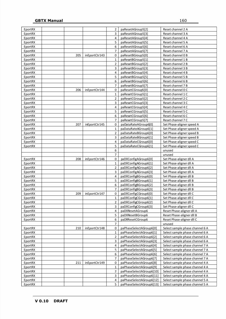
8/15/2019 gbtx Manual
http://slidepdf.com/reader/full/gbtx-manual 160/200
GBTX Manual 160
V 0.10 DRAFT
EportRX 2 paResetAGroup5[2] Reset channel 2 AEportRX 3 paResetAGroup5[3] Reset channel 3 AEportRX 4 paResetAGroup5[4] Reset channel 4 AEportRX 5 paResetAGroup5[5] Reset channel 5 AEportRX 6 paResetAGroup5[6] Reset channel 6 AEportRX 7 paResetAGroup5[7] Reset channel 7 A
EportRX 205 inEportCtr143 0 paResetBGroup5[0] Reset channel 0 BEportRX 1 paResetBGroup5[1] Reset channel 1 BEportRX 2 paResetBGroup5[2] Reset channel 2 BEportRX 3 paResetBGroup5[3] Reset channel 3 BEportRX 4 paResetBGroup5[4] Reset channel 4 BEportRX 5 paResetBGroup5[5] Reset channel 5 BEportRX 6 paResetBGroup5[6] Reset channel 6 BEportRX 7 paResetBGroup5[7] Reset channel 7 BEportRX 206 inEportCtr144 0 paResetCGroup5[0] Reset channel 0 CEportRX 1 paResetCGroup5[1] Reset channel 1 CEportRX 2 paResetCGroup5[2] Reset channel 2 CEportRX 3 paResetCGroup5[3] Reset channel 3 CEportRX 4 paResetCGroup5[4] Reset channel 4 C
EportRX 5 paResetCGroup5[5] Reset channel 5 CEportRX 6 paResetCGroup5[6] Reset channel 6 CEportRX 7 paResetCGroup5[7] Reset channel 7 CEportRX 207 inEportCtr145 0 paDataRateAGroup6[0] Set Phase-aligner speed AEportRX 1 paDataRateAGroup6[1] Set Phase-aligner speed AEportRX 2 paDataRateBGroup6[0] Set Phase-aligner speed BEportRX 3 paDataRateBGroup6[1] Set Phase-aligner speed BEportRX 4 paDataRateCGroup6[0] Set Phase-aligner speed CEportRX 5 paDataRateCGroup6[1] Set Phase-aligner speed C
6 unused7 unused
EportRX 208 inEportCtr146 0 paDllConfigAGroup6[0] Set Phase-aligner dll AEportRX 1 paDllConfigAGroup6[1] Set Phase-aligner dll A
EportRX 2 paDllConfigAGroup6[2] Set Phase-aligner dll AEportRX 3 paDllConfigAGroup6[3] Set Phase-aligner dll AEportRX 4 paDllConfigBGroup6[0] Set Phase-aligner dll BEportRX 5 paDllConfigBGroup6[1] Set Phase-aligner dll BEportRX 6 paDllConfigBGroup6[2] Set Phase-aligner dll BEportRX 7 paDllConfigBGroup6[3] Set Phase-aligner dll BEportRX 209 inEportCtr147 0 paDllConfigCGroup6[0] Set Phase-aligner dll CEportRX 1 paDllConfigCGroup6[1] Set Phase-aligner dll CEportRX 2 paDllConfigCGroup6[2] Set Phase-aligner dll CEportRX 3 paDllConfigCGroup6[3] Set Phase-aligner dll CEportRX 4 paDllResetAGroup6 Reset Phase-aligner dll AEportRX 5 paDllResetBGroup6 Reset Phase-aligner dll BEportRX 6 paDllResetCGroup6 Reset Phase-aligner dll C
7 unusedEportRX 210 inEportCtr148 0 paPhaseSelectAGroup6[0] Select sample phase channel 6 AEportRX 1 paPhaseSelectAGroup6[1] Select sample phase channel 6 AEportRX 2 paPhaseSelectAGroup6[2] Select sample phase channel 6 AEportRX 3 paPhaseSelectAGroup6[3] Select sample phase channel 6 AEportRX 4 paPhaseSelectAGroup6[4] Select sample phase channel 7 AEportRX 5 paPhaseSelectAGroup6[5] Select sample phase channel 7 AEportRX 6 paPhaseSelectAGroup6[6] Select sample phase channel 7 AEportRX 7 paPhaseSelectAGroup6[7] Select sample phase channel 7 AEportRX 211 inEportCtr149 0 paPhaseSelectAGroup6[8] Select sample phase channel 4 AEportRX 1 paPhaseSelectAGroup6[9] Select sample phase channel 4 AEportRX 2 paPhaseSelectAGroup6[10] Select sample phase channel 4 AEportRX 3 paPhaseSelectAGroup6[11] Select sample phase channel 4 A
EportRX 4 paPhaseSelectAGroup6[12] Select sample phase channel 5 AEportRX 5 paPhaseSelectAGroup6[13] Select sample phase channel 5 A
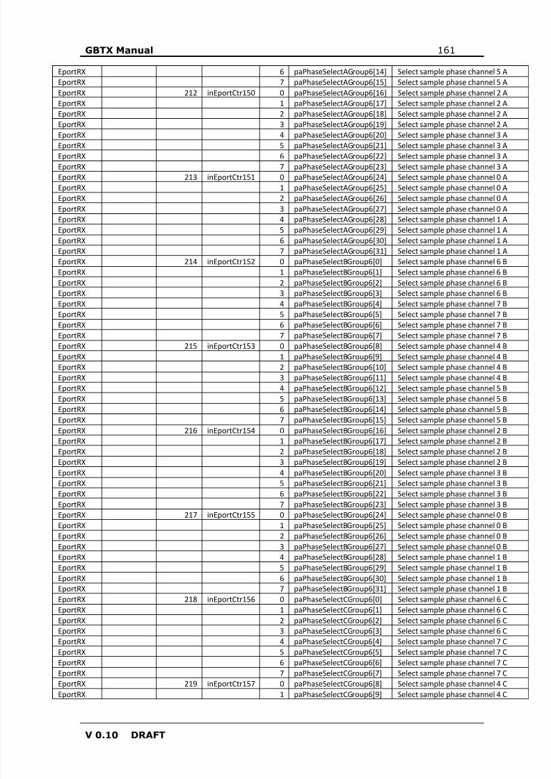
8/15/2019 gbtx Manual
http://slidepdf.com/reader/full/gbtx-manual 161/200
GBTX Manual 161
V 0.10 DRAFT
EportRX 6 paPhaseSelectAGroup6[14] Select sample phase channel 5 AEportRX 7 paPhaseSelectAGroup6[15] Select sample phase channel 5 AEportRX 212 inEportCtr150 0 paPhaseSelectAGroup6[16] Select sample phase channel 2 AEportRX 1 paPhaseSelectAGroup6[17] Select sample phase channel 2 AEportRX 2 paPhaseSelectAGroup6[18] Select sample phase channel 2 AEportRX 3 paPhaseSelectAGroup6[19] Select sample phase channel 2 A
EportRX 4 paPhaseSelectAGroup6[20] Select sample phase channel 3 AEportRX 5 paPhaseSelectAGroup6[21] Select sample phase channel 3 AEportRX 6 paPhaseSelectAGroup6[22] Select sample phase channel 3 AEportRX 7 paPhaseSelectAGroup6[23] Select sample phase channel 3 AEportRX 213 inEportCtr151 0 paPhaseSelectAGroup6[24] Select sample phase channel 0 AEportRX 1 paPhaseSelectAGroup6[25] Select sample phase channel 0 AEportRX 2 paPhaseSelectAGroup6[26] Select sample phase channel 0 AEportRX 3 paPhaseSelectAGroup6[27] Select sample phase channel 0 AEportRX 4 paPhaseSelectAGroup6[28] Select sample phase channel 1 AEportRX 5 paPhaseSelectAGroup6[29] Select sample phase channel 1 AEportRX 6 paPhaseSelectAGroup6[30] Select sample phase channel 1 AEportRX 7 paPhaseSelectAGroup6[31] Select sample phase channel 1 AEportRX 214 inEportCtr152 0 paPhaseSelectBGroup6[0] Select sample phase channel 6 B
EportRX 1 paPhaseSelectBGroup6[1] Select sample phase channel 6 BEportRX 2 paPhaseSelectBGroup6[2] Select sample phase channel 6 BEportRX 3 paPhaseSelectBGroup6[3] Select sample phase channel 6 BEportRX 4 paPhaseSelectBGroup6[4] Select sample phase channel 7 BEportRX 5 paPhaseSelectBGroup6[5] Select sample phase channel 7 BEportRX 6 paPhaseSelectBGroup6[6] Select sample phase channel 7 BEportRX 7 paPhaseSelectBGroup6[7] Select sample phase channel 7 BEportRX 215 inEportCtr153 0 paPhaseSelectBGroup6[8] Select sample phase channel 4 BEportRX 1 paPhaseSelectBGroup6[9] Select sample phase channel 4 BEportRX 2 paPhaseSelectBGroup6[10] Select sample phase channel 4 BEportRX 3 paPhaseSelectBGroup6[11] Select sample phase channel 4 BEportRX 4 paPhaseSelectBGroup6[12] Select sample phase channel 5 BEportRX 5 paPhaseSelectBGroup6[13] Select sample phase channel 5 B
EportRX 6 paPhaseSelectBGroup6[14] Select sample phase channel 5 BEportRX 7 paPhaseSelectBGroup6[15] Select sample phase channel 5 BEportRX 216 inEportCtr154 0 paPhaseSelectBGroup6[16] Select sample phase channel 2 BEportRX 1 paPhaseSelectBGroup6[17] Select sample phase channel 2 BEportRX 2 paPhaseSelectBGroup6[18] Select sample phase channel 2 BEportRX 3 paPhaseSelectBGroup6[19] Select sample phase channel 2 BEportRX 4 paPhaseSelectBGroup6[20] Select sample phase channel 3 BEportRX 5 paPhaseSelectBGroup6[21] Select sample phase channel 3 BEportRX 6 paPhaseSelectBGroup6[22] Select sample phase channel 3 BEportRX 7 paPhaseSelectBGroup6[23] Select sample phase channel 3 BEportRX 217 inEportCtr155 0 paPhaseSelectBGroup6[24] Select sample phase channel 0 BEportRX 1 paPhaseSelectBGroup6[25] Select sample phase channel 0 BEportRX 2 paPhaseSelectBGroup6[26] Select sample phase channel 0 B
EportRX 3 paPhaseSelectBGroup6[27] Select sample phase channel 0 BEportRX 4 paPhaseSelectBGroup6[28] Select sample phase channel 1 BEportRX 5 paPhaseSelectBGroup6[29] Select sample phase channel 1 BEportRX 6 paPhaseSelectBGroup6[30] Select sample phase channel 1 BEportRX 7 paPhaseSelectBGroup6[31] Select sample phase channel 1 BEportRX 218 inEportCtr156 0 paPhaseSelectCGroup6[0] Select sample phase channel 6 CEportRX 1 paPhaseSelectCGroup6[1] Select sample phase channel 6 CEportRX 2 paPhaseSelectCGroup6[2] Select sample phase channel 6 CEportRX 3 paPhaseSelectCGroup6[3] Select sample phase channel 6 CEportRX 4 paPhaseSelectCGroup6[4] Select sample phase channel 7 CEportRX 5 paPhaseSelectCGroup6[5] Select sample phase channel 7 CEportRX 6 paPhaseSelectCGroup6[6] Select sample phase channel 7 CEportRX 7 paPhaseSelectCGroup6[7] Select sample phase channel 7 C
EportRX 219 inEportCtr157 0 paPhaseSelectCGroup6[8] Select sample phase channel 4 CEportRX 1 paPhaseSelectCGroup6[9] Select sample phase channel 4 C

8/15/2019 gbtx Manual
http://slidepdf.com/reader/full/gbtx-manual 162/200
GBTX Manual 162
V 0.10 DRAFT
EportRX 2 paPhaseSelectCGroup6[10] Select sample phase channel 4 CEportRX 3 paPhaseSelectCGroup6[11] Select sample phase channel 4 CEportRX 4 paPhaseSelectCGroup6[12] Select sample phase channel 5 CEportRX 5 paPhaseSelectCGroup6[13] Select sample phase channel 5 CEportRX 6 paPhaseSelectCGroup6[14] Select sample phase channel 5 CEportRX 7 paPhaseSelectCGroup6[15] Select sample phase channel 5 C
EportRX 220 inEportCtr158 0 paPhaseSelectCGroup6[16] Select sample phase channel 2 CEportRX 1 paPhaseSelectCGroup6[17] Select sample phase channel 2 CEportRX 2 paPhaseSelectCGroup6[18] Select sample phase channel 2 CEportRX 3 paPhaseSelectCGroup6[19] Select sample phase channel 2 CEportRX 4 paPhaseSelectCGroup6[20] Select sample phase channel 3 CEportRX 5 paPhaseSelectCGroup6[21] Select sample phase channel 3 CEportRX 6 paPhaseSelectCGroup6[22] Select sample phase channel 3 CEportRX 7 paPhaseSelectCGroup6[23] Select sample phase channel 3 CEportRX 221 inEportCtr159 0 paPhaseSelectCGroup6[24] Select sample phase channel 0 CEportRX 1 paPhaseSelectCGroup6[25] Select sample phase channel 0 CEportRX 2 paPhaseSelectCGroup6[26] Select sample phase channel 0 CEportRX 3 paPhaseSelectCGroup6[27] Select sample phase channel 0 CEportRX 4 paPhaseSelectCGroup6[28] Select sample phase channel 1 C
EportRX 5 paPhaseSelectCGroup6[29] Select sample phase channel 1 CEportRX 6 paPhaseSelectCGroup6[30] Select sample phase channel 1 CEportRX 7 paPhaseSelectCGroup6[31] Select sample phase channel 1 CEportRX 222 inEportCtr160 0 paTrainAGroup6[0] Train channel 0 AEportRX 1 paTrainAGroup6[1] Train channel 1 AEportRX 2 paTrainAGroup6[2] Train channel 2 AEportRX 3 paTrainAGroup6[3] Train channel 3 AEportRX 4 paTrainAGroup6[4] Train channel 4 AEportRX 5 paTrainAGroup6[5] Train channel 5 AEportRX 6 paTrainAGroup6[6] Train channel 6 AEportRX 7 paTrainAGroup6[7] Train channel 7 AEportRX 223 inEportCtr161 0 paTrainBGroup6[0] Train channel 0 BEportRX 1 paTrainBGroup6[1] Train channel 1 B
EportRX 2 paTrainBGroup6[2] Train channel 2 BEportRX 3 paTrainBGroup6[3] Train channel 3 BEportRX 4 paTrainBGroup6[4] Train channel 4 BEportRX 5 paTrainBGroup6[5] Train channel 5 BEportRX 6 paTrainBGroup6[6] Train channel 6 BEportRX 7 paTrainBGroup6[7] Train channel 7 BEportRX 224 inEportCtr162 0 paTrainCGroup6[0] Train channel 0 CEportRX 1 paTrainCGroup6[1] Train channel 1 CEportRX 2 paTrainCGroup6[2] Train channel 2 CEportRX 3 paTrainCGroup6[3] Train channel 3 CEportRX 4 paTrainCGroup6[4] Train channel 4 CEportRX 5 paTrainCGroup6[5] Train channel 5 CEportRX 6 paTrainCGroup6[6] Train channel 6 C
EportRX 7 paTrainCGroup6[7] Train channel 7 CEportRX 225 inEportCtr163 0 paEnableAGroup6[0] Enable channel 0 AEportRX 1 paEnableAGroup6[1] Enable channel 1 AEportRX 2 paEnableAGroup6[2] Enable channel 2 AEportRX 3 paEnableAGroup6[3] Enable channel 3 AEportRX 4 paEnableAGroup6[4] Enable channel 4 AEportRX 5 paEnableAGroup6[5] Enable channel 5 AEportRX 6 paEnableAGroup6[6] Enable channel 6 AEportRX 7 paEnableAGroup6[7] Enable channel 7 AEportRX 226 inEportCtr164 0 paEnableBGroup6[0] Enable channel 0 BEportRX 1 paEnableBGroup6[1] Enable channel 1 BEportRX 2 paEnableBGroup6[2] Enable channel 2 BEportRX 3 paEnableBGroup6[3] Enable channel 3 B
EportRX 4 paEnableBGroup6[4] Enable channel 4 BEportRX 5 paEnableBGroup6[5] Enable channel 5 B
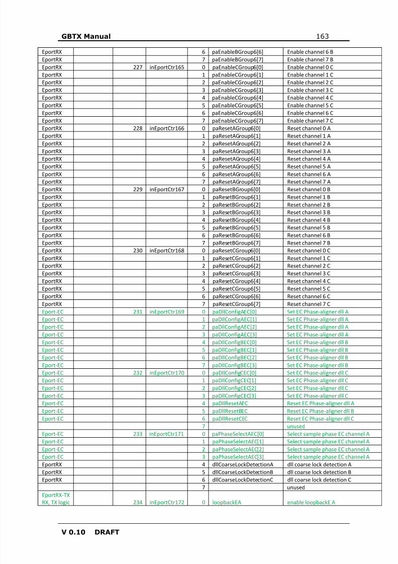
8/15/2019 gbtx Manual
http://slidepdf.com/reader/full/gbtx-manual 163/200
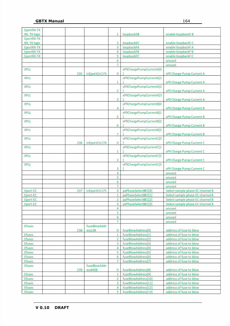
8/15/2019 gbtx Manual
http://slidepdf.com/reader/full/gbtx-manual 164/200
GBTX Manual 164
V 0.10 DRAFT
EportRX-TXRX, TX logic 1 loopbackEB enable loopbackE BEportRX-TXRX, TX logic 2 loopbackEC enable loopbackE CEportRX-TX 3 loopbackFA enable loopbackF AEportRX-TX 4 loopbackFB enable loopbackF B
EportRX-TX 5 loopbackFC enable loopbackF C6 unused7 unused
XPLL235 inEportCtr173 0
xPllChargePumpCurrentA[0] xPll Charge Pump Current A
XPLL 1
xPllChargePumpCurrentA[1] xPll Charge Pump Current A
XPLL 2
xPllChargePumpCurrentA[2] xPll Charge Pump Current A
XPLL 3
xPllChargePumpCurrentA[3] xPll Charge Pump Current A
XPLL 4
xPllChargePumpCurrentB[0] xPll Charge Pump Current B
XPLL 5 xPllChargePumpCurrentB[1] xPll Charge Pump Current BXPLL
6xPllChargePumpCurrentB[2] xPll Charge Pump Current B
XPLL 7
xPllChargePumpCurrentB[3] xPll Charge Pump Current B
XPLL 236 inEportCtr174 0
xPllChargePumpCurrentC[0] xPll Charge Pump Current C
XPLL 1
xPllChargePumpCurrentC[1] xPll Charge Pump Current C
XPLL 2
xPllChargePumpCurrentC[2] xPll Charge Pump Current C
XPLL 3
xPllChargePumpCurrentC[3] xPll Charge Pump Current C
4 unused5 unused6 unused7 unused
Eport-EC 237 inEportCtr175 0 paPhaseSelectBEC[0] Select sample phase EC channel BEport-EC 1 paPhaseSelectBEC[1] Select sample phase EC channel BEport-EC 2 paPhaseSelectBEC[2] Select sample phase EC channel BEport-EC 3 paPhaseSelectBEC[3] Select sample phase EC channel B
4 unused5 unused6 unused7 unused
Efuses238
fuseBlowAddressLSB 0 fuseBlowAddress[0] address of fuse to blow
Efuses 1 fuseBlowAddress[1] address of fuse to blowEfuses 2 fuseBlowAddress[2] address of fuse to blowEfuses 3 fuseBlowAddress[3] address of fuse to blowEfuses 4 fuseBlowAddress[4] address of fuse to blowEfuses 5 fuseBlowAddress[5] address of fuse to blowEfuses 6 fuseBlowAddress[6] address of fuse to blowEfuses 7 fuseBlowAddress[7] address of fuse to blowEfuses
239fuseBlowAddressMSB 0 fuseBlowAddress[8] address of fuse to blow
Efuses 1 fuseBlowAddress[9] address of fuse to blowEfuses 2 fuseBlowAddress[10] address of fuse to blowEfuses 3 fuseBlowAddress[11] address of fuse to blowEfuses 4 fuseBlowAddress[12] address of fuse to blowEfuses 5 fuseBlowAddress[13] address of fuse to blow
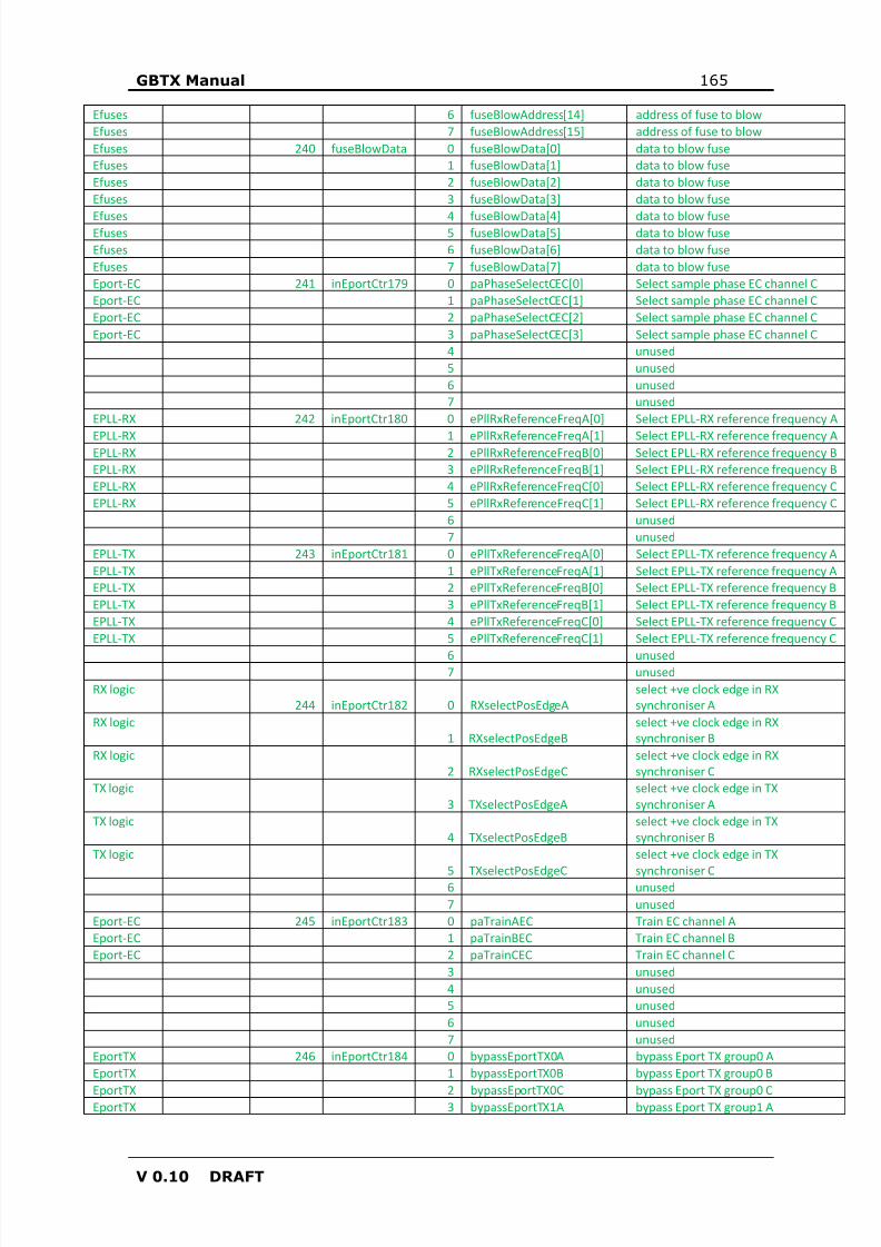
8/15/2019 gbtx Manual
http://slidepdf.com/reader/full/gbtx-manual 165/200
GBTX Manual 165
V 0.10 DRAFT
Efuses 6 fuseBlowAddress[14] address of fuse to blowEfuses 7 fuseBlowAddress[15] address of fuse to blowEfuses 240 fuseBlowData 0 fuseBlowData[0] data to blow fuseEfuses 1 fuseBlowData[1] data to blow fuseEfuses 2 fuseBlowData[2] data to blow fuseEfuses 3 fuseBlowData[3] data to blow fuse
Efuses 4 fuseBlowData[4] data to blow fuseEfuses 5 fuseBlowData[5] data to blow fuseEfuses 6 fuseBlowData[6] data to blow fuseEfuses 7 fuseBlowData[7] data to blow fuseEport-EC 241 inEportCtr179 0 paPhaseSelectCEC[0] Select sample phase EC channel CEport-EC 1 paPhaseSelectCEC[1] Select sample phase EC channel CEport-EC 2 paPhaseSelectCEC[2] Select sample phase EC channel CEport-EC 3 paPhaseSelectCEC[3] Select sample phase EC channel C
4 unused5 unused6 unused7 unused
EPLL-RX 242 inEportCtr180 0 ePllRxReferenceFreqA[0] Select EPLL-RX reference frequency A
EPLL-RX 1 ePllRxReferenceFreqA[1] Select EPLL-RX reference frequency AEPLL-RX 2 ePllRxReferenceFreqB[0] Select EPLL-RX reference frequency BEPLL-RX 3 ePllRxReferenceFreqB[1] Select EPLL-RX reference frequency BEPLL-RX 4 ePllRxReferenceFreqC[0] Select EPLL-RX reference frequency CEPLL-RX 5 ePllRxReferenceFreqC[1] Select EPLL-RX reference frequency C
6 unused7 unused
EPLL-TX 243 inEportCtr181 0 ePllTxReferenceFreqA[0] Select EPLL-TX reference frequency AEPLL-TX 1 ePllTxReferenceFreqA[1] Select EPLL-TX reference frequency AEPLL-TX 2 ePllTxReferenceFreqB[0] Select EPLL-TX reference frequency BEPLL-TX 3 ePllTxReferenceFreqB[1] Select EPLL-TX reference frequency BEPLL-TX 4 ePllTxReferenceFreqC[0] Select EPLL-TX reference frequency CEPLL-TX 5 ePllTxReferenceFreqC[1] Select EPLL-TX reference frequency C
6 unused7 unused
RX logic244 inEportCtr182 0 RXselectPosEdgeA
select +ve clock edge in RXsynchroniser A
RX logic 1 RXselectPosEdgeB
select +ve clock edge in RXsynchroniser B
RX logic 2 RXselectPosEdgeC
select +ve clock edge in RXsynchroniser C
TX logic3 TXselectPosEdgeA
select +ve clock edge in TXsynchroniser A
TX logic 4 TXselectPosEdgeB
select +ve clock edge in TXsynchroniser B
TX logic
5 TXselectPosEdgeC
select +ve clock edge in TX
synchroniser C6 unused7 unused
Eport-EC 245 inEportCtr183 0 paTrainAEC Train EC channel AEport-EC 1 paTrainBEC Train EC channel BEport-EC 2 paTrainCEC Train EC channel C
3 unused4 unused5 unused6 unused7 unused
EportTX 246 inEportCtr184 0 bypassEportTX0A bypass Eport TX group0 AEportTX 1 bypassEportTX0B bypass Eport TX group0 B
EportTX 2 bypassEportTX0C bypass Eport TX group0 CEportTX 3 bypassEportTX1A bypass Eport TX group1 A
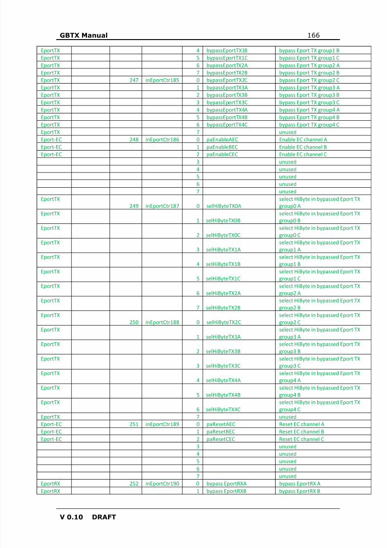
8/15/2019 gbtx Manual
http://slidepdf.com/reader/full/gbtx-manual 166/200
GBTX Manual 166
V 0.10 DRAFT
EportTX 4 bypassEportTX1B bypass Eport TX group1 BEportTX 5 bypassEportTX1C bypass Eport TX group1 CEportTX 6 bypassEportTX2A bypass Eport TX group2 AEportTX 7 bypassEportTX2B bypass Eport TX group2 BEportTX 247 inEportCtr185 0 bypassEportTX2C bypass Eport TX group2 CEportTX 1 bypassEportTX3A bypass Eport TX group3 A
EportTX 2 bypassEportTX3B bypass Eport TX group3 BEportTX 3 bypassEportTX3C bypass Eport TX group3 CEportTX 4 bypassEportTX4A bypass Eport TX group4 AEportTX 5 bypassEportTX4B bypass Eport TX group4 BEportTX 6 bypassEportTX4C bypass Eport TX group4 CEportTX 7 unusedEport-EC 248 inEportCtr186 0 paEnableAEC Enable EC channel AEport-EC 1 paEnableBEC Enable EC channel BEport-EC 2 paEnableCEC Enable EC channel C
3 unused4 unused5 unused6 unused
7 unusedEportTX
249 inEportCtr187 0 selHiByteTX0Aselect HiByte in bypassed Eport TXgroup0 A
EportTX 1 selHiByteTX0B
select HiByte in bypassed Eport TXgroup0 B
EportTX 2 selHiByteTX0C
select HiByte in bypassed Eport TXgroup0 C
EportTX 3 selHiByteTX1A
select HiByte in bypassed Eport TXgroup1 A
EportTX4 selHiByteTX1B
select HiByte in bypassed Eport TXgroup1 B
EportTX 5 selHiByteTX1C
select HiByte in bypassed Eport TXgroup1 C
EportTX 6 selHiByteTX2A select HiByte in bypassed Eport TXgroup2 AEportTX
7 selHiByteTX2Bselect HiByte in bypassed Eport TXgroup2 B
EportTX250 inEportCtr188 0 selHiByteTX2C
select HiByte in bypassed Eport TXgroup2 C
EportTX 1 selHiByteTX3A
select HiByte in bypassed Eport TXgroup3 A
EportTX 2 selHiByteTX3B
select HiByte in bypassed Eport TXgroup3 B
EportTX 3 selHiByteTX3C
select HiByte in bypassed Eport TXgroup3 C
EportTX4 selHiByteTX4A
select HiByte in bypassed Eport TXgroup4 A
EportTX 5 selHiByteTX4B
select HiByte in bypassed Eport TXgroup4 B
EportTX 6 selHiByteTX4C
select HiByte in bypassed Eport TXgroup4 C
EportTX 7 unusedEport-EC 251 inEportCtr189 0 paResetAEC Reset EC channel AEport-EC 1 paResetBEC Reset EC channel BEport-EC 2 paResetCEC Reset EC channel C
3 unused4 unused5 unused6 unused7 unused
EportRX 252 inEportCtr190 0 bypass EportRXA bypass EportRX AEportRX 1 bypass EportRXB bypass EportRX B
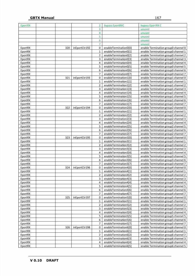
8/15/2019 gbtx Manual
http://slidepdf.com/reader/full/gbtx-manual 167/200
GBTX Manual 167
V 0.10 DRAFT
EportRX 2 bypass EportRXC bypass EportRX C3 unused4 unused5 unused6 unused7 unused
EportRX 320 inEportCtr192 0 enableTermination0[0] enable Termination group0 channel 0EportRX 1 enableTermination0[1] enable Termination group0 channel 1EportRX 2 enableTermination0[2] enable Termination group0 channel 2EportRX 3 enableTermination0[3] enable Termination group0 channel 3EportRX 4 enableTermination0[4] enable Termination group0 channel 4EportRX 5 enableTermination0[5] enable Termination group0 channel 5EportRX 6 enableTermination0[6] enable Termination group0 channel 6EportRX 7 enableTermination0[7] enable Termination group0 channel 7EportRX 321 inEportCtr193 0 enableTermination1[0] enable Termination group1 channel 0EportRX 1 enableTermination1[1] enable Termination group1 channel 1EportRX 2 enableTermination1[2] enable Termination group1 channel 2EportRX 3 enableTermination1[3] enable Termination group1 channel 3EportRX 4 enableTermination1[4] enable Termination group1 channel 4
EportRX 5 enableTermination1[5] enable Termination group1 channel 5EportRX 6 enableTermination1[6] enable Termination group1 channel 6EportRX 7 enableTermination1[7] enable Termination group1 channel 7EportRX 322 inEportCtr194 0 enableTermination2[0] enable Termination group2 channel 0EportRX 1 enableTermination2[1] enable Termination group2 channel 1EportRX 2 enableTermination2[2] enable Termination group2 channel 2EportRX 3 enableTermination2[3] enable Termination group2 channel 3EportRX 4 enableTermination2[4] enable Termination group2 channel 4EportRX 5 enableTermination2[5] enable Termination group2 channel 5EportRX 6 enableTermination2[6] enable Termination group2 channel 6EportRX 7 enableTermination2[7] enable Termination group2 channel 7EportRX 323 inEportCtr195 0 enableTermination3[0] enable Termination group3 channel 0EportRX 1 enableTermination3[1] enable Termination group3 channel 1
EportRX 2 enableTermination3[2] enable Termination group3 channel 2EportRX 3 enableTermination3[3] enable Termination group3 channel 3EportRX 4 enableTermination3[4] enable Termination group3 channel 4EportRX 5 enableTermination3[5] enable Termination group3 channel 5EportRX 6 enableTermination3[6] enable Termination group3 channel 6EportRX 7 enableTermination3[7] enable Termination group3 channel 7EportRX 324 inEportCtr196 0 enableTermination4[0] enable Termination group4 channel 0EportRX 1 enableTermination4[1] enable Termination group4 channel 1EportRX 2 enableTermination4[2] enable Termination group4 channel 2EportRX 3 enableTermination4[3] enable Termination group4 channel 3EportRX 4 enableTermination4[4] enable Termination group4 channel 4EportRX 5 enableTermination4[5] enable Termination group4 channel 5EportRX 6 enableTermination4[6] enable Termination group4 channel 6
EportRX 7 enableTermination4[7] enable Termination group4 channel 7EportRX 325 inEportCtr197 0 enableTermination5[0] enable Termination group5 channel 0EportRX 1 enableTermination5[1] enable Termination group5 channel 1EportRX 2 enableTermination5[2] enable Termination group5 channel 2EportRX 3 enableTermination5[3] enable Termination group5 channel 3EportRX 4 enableTermination5[4] enable Termination group5 channel 4EportRX 5 enableTermination5[5] enable Termination group5 channel 5EportRX 6 enableTermination5[6] enable Termination group5 channel 6EportRX 7 enableTermination5[7] enable Termination group5 channel 7EportRX 326 inEportCtr198 0 enableTermination6[0] enable Termination group6 channel 0EportRX 1 enableTermination6[1] enable Termination group6 channel 1EportRX 2 enableTermination6[2] enable Termination group6 channel 2EportRX 3 enableTermination6[3] enable Termination group6 channel 3
EportRX 4 enableTermination6[4] enable Termination group6 channel 4EportRX 5 enableTermination6[5] enable Termination group6 channel 5

8/15/2019 gbtx Manual
http://slidepdf.com/reader/full/gbtx-manual 168/200
GBTX Manual 168
V 0.10 DRAFT
EportRX 6 enableTermination6[6] enable Termination group6 channel 6EportRX 7 enableTermination6[7] enable Termination group6 channel 7
Ttt
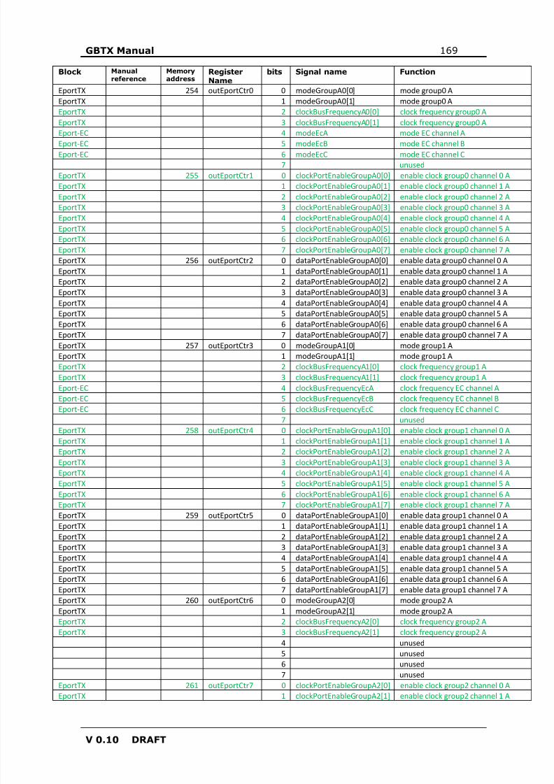
8/15/2019 gbtx Manual
http://slidepdf.com/reader/full/gbtx-manual 169/200
GBTX Manual 169
V 0.10 DRAFT
Block Manualreference
Memoryaddress
RegisterName
bits Signal name Function
EportTX 254 outEportCtr0 0 modeGroupA0[0] mode group0 AEportTX 1 modeGroupA0[1] mode group0 AEportTX 2 clockBusFrequencyA0[0] clock frequency group0 AEportTX 3 clockBusFrequencyA0[1] clock frequency group0 AEport-EC 4 modeEcA mode EC channel AEport-EC 5 modeEcB mode EC channel BEport-EC 6 modeEcC mode EC channel C
7 unusedEportTX 255 outEportCtr1 0 clockPortEnableGroupA0[0] enable clock group0 channel 0 AEportTX 1 clockPortEnableGroupA0[1] enable clock group0 channel 1 AEportTX 2 clockPortEnableGroupA0[2] enable clock group0 channel 2 AEportTX 3 clockPortEnableGroupA0[3] enable clock group0 channel 3 AEportTX 4 clockPortEnableGroupA0[4] enable clock group0 channel 4 AEportTX 5 clockPortEnableGroupA0[5] enable clock group0 channel 5 AEportTX 6 clockPortEnableGroupA0[6] enable clock group0 channel 6 AEportTX 7 clockPortEnableGroupA0[7] enable clock group0 channel 7 AEportTX 256 outEportCtr2 0 dataPortEnableGroupA0[0] enable data group0 channel 0 A
EportTX 1 dataPortEnableGroupA0[1] enable data group0 channel 1 AEportTX 2 dataPortEnableGroupA0[2] enable data group0 channel 2 AEportTX 3 dataPortEnableGroupA0[3] enable data group0 channel 3 AEportTX 4 dataPortEnableGroupA0[4] enable data group0 channel 4 AEportTX 5 dataPortEnableGroupA0[5] enable data group0 channel 5 AEportTX 6 dataPortEnableGroupA0[6] enable data group0 channel 6 AEportTX 7 dataPortEnableGroupA0[7] enable data group0 channel 7 AEportTX 257 outEportCtr3 0 modeGroupA1[0] mode group1 AEportTX 1 modeGroupA1[1] mode group1 AEportTX 2 clockBusFrequencyA1[0] clock frequency group1 AEportTX 3 clockBusFrequencyA1[1] clock frequency group1 AEport-EC 4 clockBusFrequencyEcA clock frequency EC channel AEport-EC 5 clockBusFrequencyEcB clock frequency EC channel B
Eport-EC 6 clockBusFrequencyEcC clock frequency EC channel C7 unusedEportTX 258 outEportCtr4 0 clockPortEnableGroupA1[0] enable clock group1 channel 0 AEportTX 1 clockPortEnableGroupA1[1] enable clock group1 channel 1 AEportTX 2 clockPortEnableGroupA1[2] enable clock group1 channel 2 AEportTX 3 clockPortEnableGroupA1[3] enable clock group1 channel 3 AEportTX 4 clockPortEnableGroupA1[4] enable clock group1 channel 4 AEportTX 5 clockPortEnableGroupA1[5] enable clock group1 channel 5 AEportTX 6 clockPortEnableGroupA1[6] enable clock group1 channel 6 AEportTX 7 clockPortEnableGroupA1[7] enable clock group1 channel 7 AEportTX 259 outEportCtr5 0 dataPortEnableGroupA1[0] enable data group1 channel 0 AEportTX 1 dataPortEnableGroupA1[1] enable data group1 channel 1 AEportTX 2 dataPortEnableGroupA1[2] enable data group1 channel 2 A
EportTX 3 dataPortEnableGroupA1[3] enable data group1 channel 3 AEportTX 4 dataPortEnableGroupA1[4] enable data group1 channel 4 AEportTX 5 dataPortEnableGroupA1[5] enable data group1 channel 5 AEportTX 6 dataPortEnableGroupA1[6] enable data group1 channel 6 AEportTX 7 dataPortEnableGroupA1[7] enable data group1 channel 7 AEportTX 260 outEportCtr6 0 modeGroupA2[0] mode group2 AEportTX 1 modeGroupA2[1] mode group2 AEportTX 2 clockBusFrequencyA2[0] clock frequency group2 AEportTX 3 clockBusFrequencyA2[1] clock frequency group2 A
4 unused5 unused6 unused7 unused
EportTX 261 outEportCtr7 0 clockPortEnableGroupA2[0] enable clock group2 channel 0 AEportTX 1 clockPortEnableGroupA2[1] enable clock group2 channel 1 A
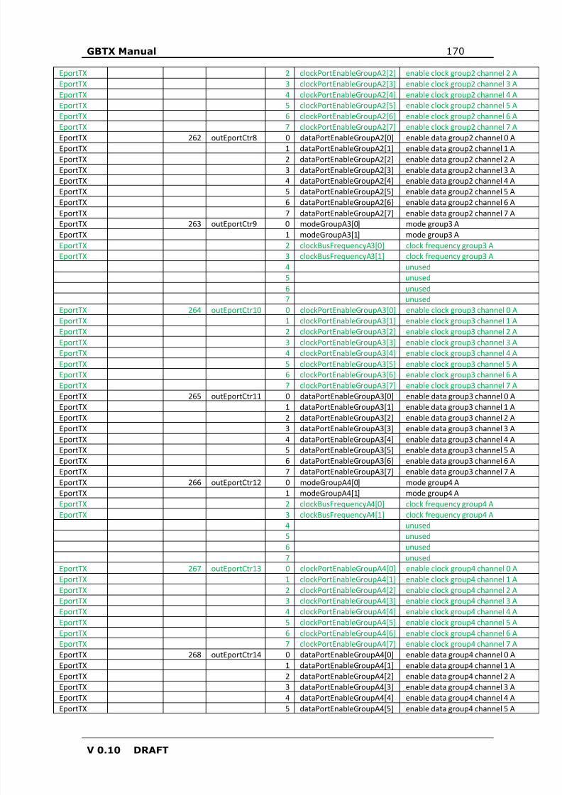
8/15/2019 gbtx Manual
http://slidepdf.com/reader/full/gbtx-manual 170/200
GBTX Manual 170
V 0.10 DRAFT
EportTX 2 clockPortEnableGroupA2[2] enable clock group2 channel 2 AEportTX 3 clockPortEnableGroupA2[3] enable clock group2 channel 3 AEportTX 4 clockPortEnableGroupA2[4] enable clock group2 channel 4 AEportTX 5 clockPortEnableGroupA2[5] enable clock group2 channel 5 AEportTX 6 clockPortEnableGroupA2[6] enable clock group2 channel 6 AEportTX 7 clockPortEnableGroupA2[7] enable clock group2 channel 7 A
EportTX 262 outEportCtr8 0 dataPortEnableGroupA2[0] enable data group2 channel 0 AEportTX 1 dataPortEnableGroupA2[1] enable data group2 channel 1 AEportTX 2 dataPortEnableGroupA2[2] enable data group2 channel 2 AEportTX 3 dataPortEnableGroupA2[3] enable data group2 channel 3 AEportTX 4 dataPortEnableGroupA2[4] enable data group2 channel 4 AEportTX 5 dataPortEnableGroupA2[5] enable data group2 channel 5 AEportTX 6 dataPortEnableGroupA2[6] enable data group2 channel 6 AEportTX 7 dataPortEnableGroupA2[7] enable data group2 channel 7 AEportTX 263 outEportCtr9 0 modeGroupA3[0] mode group3 AEportTX 1 modeGroupA3[1] mode group3 AEportTX 2 clockBusFrequencyA3[0] clock frequency group3 AEportTX 3 clockBusFrequencyA3[1] clock frequency group3 A
4 unused
5 unused6 unused7 unused
EportTX 264 outEportCtr10 0 clockPortEnableGroupA3[0] enable clock group3 channel 0 AEportTX 1 clockPortEnableGroupA3[1] enable clock group3 channel 1 AEportTX 2 clockPortEnableGroupA3[2] enable clock group3 channel 2 AEportTX 3 clockPortEnableGroupA3[3] enable clock group3 channel 3 AEportTX 4 clockPortEnableGroupA3[4] enable clock group3 channel 4 AEportTX 5 clockPortEnableGroupA3[5] enable clock group3 channel 5 AEportTX 6 clockPortEnableGroupA3[6] enable clock group3 channel 6 AEportTX 7 clockPortEnableGroupA3[7] enable clock group3 channel 7 AEportTX 265 outEportCtr11 0 dataPortEnableGroupA3[0] enable data group3 channel 0 AEportTX 1 dataPortEnableGroupA3[1] enable data group3 channel 1 A
EportTX 2 dataPortEnableGroupA3[2] enable data group3 channel 2 AEportTX 3 dataPortEnableGroupA3[3] enable data group3 channel 3 AEportTX 4 dataPortEnableGroupA3[4] enable data group3 channel 4 AEportTX 5 dataPortEnableGroupA3[5] enable data group3 channel 5 AEportTX 6 dataPortEnableGroupA3[6] enable data group3 channel 6 AEportTX 7 dataPortEnableGroupA3[7] enable data group3 channel 7 AEportTX 266 outEportCtr12 0 modeGroupA4[0] mode group4 AEportTX 1 modeGroupA4[1] mode group4 AEportTX 2 clockBusFrequencyA4[0] clock frequency group4 AEportTX 3 clockBusFrequencyA4[1] clock frequency group4 A
4 unused5 unused6 unused
7 unusedEportTX 267 outEportCtr13 0 clockPortEnableGroupA4[0] enable clock group4 channel 0 AEportTX 1 clockPortEnableGroupA4[1] enable clock group4 channel 1 AEportTX 2 clockPortEnableGroupA4[2] enable clock group4 channel 2 AEportTX 3 clockPortEnableGroupA4[3] enable clock group4 channel 3 AEportTX 4 clockPortEnableGroupA4[4] enable clock group4 channel 4 AEportTX 5 clockPortEnableGroupA4[5] enable clock group4 channel 5 AEportTX 6 clockPortEnableGroupA4[6] enable clock group4 channel 6 AEportTX 7 clockPortEnableGroupA4[7] enable clock group4 channel 7 AEportTX 268 outEportCtr14 0 dataPortEnableGroupA4[0] enable data group4 channel 0 AEportTX 1 dataPortEnableGroupA4[1] enable data group4 channel 1 AEportTX 2 dataPortEnableGroupA4[2] enable data group4 channel 2 AEportTX 3 dataPortEnableGroupA4[3] enable data group4 channel 3 A
EportTX 4 dataPortEnableGroupA4[4] enable data group4 channel 4 AEportTX 5 dataPortEnableGroupA4[5] enable data group4 channel 5 A
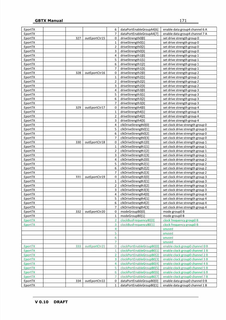
8/15/2019 gbtx Manual
http://slidepdf.com/reader/full/gbtx-manual 171/200
GBTX Manual 171
V 0.10 DRAFT
EportTX 6 dataPortEnableGroupA4[6] enable data group4 channel 6 AEportTX 7 dataPortEnableGroupA4[7] enable data group4 channel 7 AEportTX 327 outEportCtr15 0 driveStrength0[0] set drive strength group 0EportTX 1 driveStrength0[1] set drive strength group 0EportTX 2 driveStrength0[2] set drive strength group 0EportTX 3 driveStrength0[3] set drive strength group 0
EportTX 4 driveStrength1[0] set drive strength group 1EportTX 5 driveStrength1[1] set drive strength group 1EportTX 6 driveStrength1[2] set drive strength group 1EportTX 7 driveStrength1[3] set drive strength group 1EportTX 328 outEportCtr16 0 driveStrength2[0] set drive strength group 2EportTX 1 driveStrength2[1] set drive strength group 2EportTX 2 driveStrength2[2] set drive strength group 2EportTX 3 driveStrength2[3] set drive strength group 2EportTX 4 driveStrength3[0] set drive strength group 3EportTX 5 driveStrength3[1] set drive strength group 3EportTX 6 driveStrength3[2] set drive strength group 3EportTX 7 driveStrength3[3] set drive strength group 3EportTX 329 outEportCtr17 0 driveStrength4[0] set drive strength group 4
EportTX 1 driveStrength4[1] set drive strength group 4EportTX 2 driveStrength4[2] set drive strength group 4EportTX 3 driveStrength4[3] set drive strength group 4EportTX 4 clkDriveStrength0[0] set clock drive strength group 0EportTX 5 clkDriveStrength0[1] set clock drive strength group 0EportTX 6 clkDriveStrength0[2] set clock drive strength group 0EportTX 7 clkDriveStrength0[3] set clock drive strength group 0EportTX 330 outEportCtr18 0 clkDriveStrength1[0] set clock drive strength group 1EportTX 1 clkDriveStrength1[1] set clock drive strength group 1EportTX 2 clkDriveStrength1[2] set clock drive strength group 1EportTX 3 clkDriveStrength1[3] set clock drive strength group 1EportTX 4 clkDriveStrength2[0] set clock drive strength group 2EportTX 5 clkDriveStrength2[1] set clock drive strength group 2
EportTX 6 clkDriveStrength2[2] set clock drive strength group 2EportTX 7 clkDriveStrength2[3] set clock drive strength group 2EportTX 331 outEportCtr19 0 clkDriveStrength3[0] set clock drive strength group 3EportTX 1 clkDriveStrength3[1] set clock drive strength group 3EportTX 2 clkDriveStrength3[2] set clock drive strength group 3EportTX 3 clkDriveStrength3[3] set clock drive strength group 3EportTX 4 clkDriveStrength4[0] set clock drive strength group 4EportTX 5 clkDriveStrength4[1] set clock drive strength group 4EportTX 6 clkDriveStrength4[2] set clock drive strength group 4EportTX 7 clkDriveStrength4[3] set clock drive strength group 4EportTX 332 outEportCtr20 0 modeGroupB0[0] mode group0 BEportTX 1 modeGroupB0[1] mode group0 BEportTX 2 clockBusFrequencyB0[0] clock frequency group0 B
EportTX 3 clockBusFrequencyB0[1] clock frequency group0 B4 unused5 unused6 unused7 unused
EportTX 333 outEportCtr21 0 clockPortEnableGroupB0[0] enable clock group0 channel 0 BEportTX 1 clockPortEnableGroupB0[1] enable clock group0 channel 1 BEportTX 2 clockPortEnableGroupB0[2] enable clock group0 channel 2 BEportTX 3 clockPortEnableGroupB0[3] enable clock group0 channel 3 BEportTX 4 clockPortEnableGroupB0[4] enable clock group0 channel 4 BEportTX 5 clockPortEnableGroupB0[5] enable clock group0 channel 5 BEportTX 6 clockPortEnableGroupB0[6] enable clock group0 channel 6 BEportTX 7 clockPortEnableGroupB0[7] enable clock group0 channel 7 B
EportTX 334 outEportCtr22 0 dataPortEnableGroupB0[0] enable data group0 channel 0 BEportTX 1 dataPortEnableGroupB0[1] enable data group0 channel 1 B
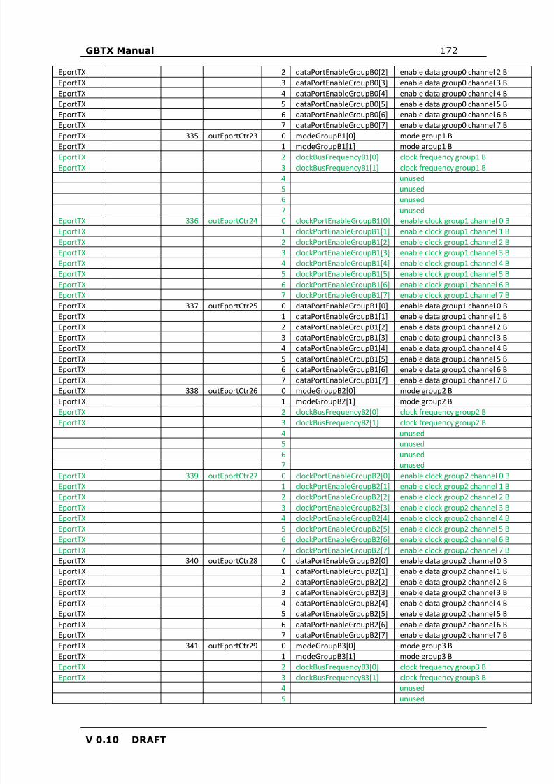
8/15/2019 gbtx Manual
http://slidepdf.com/reader/full/gbtx-manual 172/200
GBTX Manual 172
V 0.10 DRAFT
EportTX 2 dataPortEnableGroupB0[2] enable data group0 channel 2 BEportTX 3 dataPortEnableGroupB0[3] enable data group0 channel 3 BEportTX 4 dataPortEnableGroupB0[4] enable data group0 channel 4 BEportTX 5 dataPortEnableGroupB0[5] enable data group0 channel 5 BEportTX 6 dataPortEnableGroupB0[6] enable data group0 channel 6 BEportTX 7 dataPortEnableGroupB0[7] enable data group0 channel 7 B
EportTX 335 outEportCtr23 0 modeGroupB1[0] mode group1 BEportTX 1 modeGroupB1[1] mode group1 BEportTX 2 clockBusFrequencyB1[0] clock frequency group1 BEportTX 3 clockBusFrequencyB1[1] clock frequency group1 B
4 unused5 unused6 unused7 unused
EportTX 336 outEportCtr24 0 clockPortEnableGroupB1[0] enable clock group1 channel 0 BEportTX 1 clockPortEnableGroupB1[1] enable clock group1 channel 1 BEportTX 2 clockPortEnableGroupB1[2] enable clock group1 channel 2 BEportTX 3 clockPortEnableGroupB1[3] enable clock group1 channel 3 BEportTX 4 clockPortEnableGroupB1[4] enable clock group1 channel 4 B
EportTX 5 clockPortEnableGroupB1[5] enable clock group1 channel 5 BEportTX 6 clockPortEnableGroupB1[6] enable clock group1 channel 6 BEportTX 7 clockPortEnableGroupB1[7] enable clock group1 channel 7 BEportTX 337 outEportCtr25 0 dataPortEnableGroupB1[0] enable data group1 channel 0 BEportTX 1 dataPortEnableGroupB1[1] enable data group1 channel 1 BEportTX 2 dataPortEnableGroupB1[2] enable data group1 channel 2 BEportTX 3 dataPortEnableGroupB1[3] enable data group1 channel 3 BEportTX 4 dataPortEnableGroupB1[4] enable data group1 channel 4 BEportTX 5 dataPortEnableGroupB1[5] enable data group1 channel 5 BEportTX 6 dataPortEnableGroupB1[6] enable data group1 channel 6 BEportTX 7 dataPortEnableGroupB1[7] enable data group1 channel 7 BEportTX 338 outEportCtr26 0 modeGroupB2[0] mode group2 BEportTX 1 modeGroupB2[1] mode group2 B
EportTX 2 clockBusFrequencyB2[0] clock frequency group2 BEportTX 3 clockBusFrequencyB2[1] clock frequency group2 B
4 unused5 unused6 unused7 unused
EportTX 339 outEportCtr27 0 clockPortEnableGroupB2[0] enable clock group2 channel 0 BEportTX 1 clockPortEnableGroupB2[1] enable clock group2 channel 1 BEportTX 2 clockPortEnableGroupB2[2] enable clock group2 channel 2 BEportTX 3 clockPortEnableGroupB2[3] enable clock group2 channel 3 BEportTX 4 clockPortEnableGroupB2[4] enable clock group2 channel 4 BEportTX 5 clockPortEnableGroupB2[5] enable clock group2 channel 5 BEportTX 6 clockPortEnableGroupB2[6] enable clock group2 channel 6 B
EportTX 7 clockPortEnableGroupB2[7] enable clock group2 channel 7 BEportTX 340 outEportCtr28 0 dataPortEnableGroupB2[0] enable data group2 channel 0 BEportTX 1 dataPortEnableGroupB2[1] enable data group2 channel 1 BEportTX 2 dataPortEnableGroupB2[2] enable data group2 channel 2 BEportTX 3 dataPortEnableGroupB2[3] enable data group2 channel 3 BEportTX 4 dataPortEnableGroupB2[4] enable data group2 channel 4 BEportTX 5 dataPortEnableGroupB2[5] enable data group2 channel 5 BEportTX 6 dataPortEnableGroupB2[6] enable data group2 channel 6 BEportTX 7 dataPortEnableGroupB2[7] enable data group2 channel 7 BEportTX 341 outEportCtr29 0 modeGroupB3[0] mode group3 BEportTX 1 modeGroupB3[1] mode group3 BEportTX 2 clockBusFrequencyB3[0] clock frequency group3 BEportTX 3 clockBusFrequencyB3[1] clock frequency group3 B
4 unused5 unused
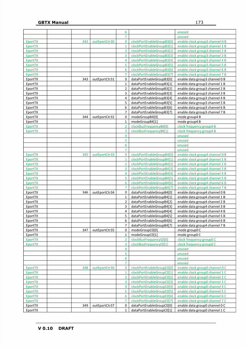
8/15/2019 gbtx Manual
http://slidepdf.com/reader/full/gbtx-manual 173/200
GBTX Manual 173
V 0.10 DRAFT
6 unused7 unused
EportTX 342 outEportCtr30 0 clockPortEnableGroupB3[0] enable clock group3 channel 0 BEportTX 1 clockPortEnableGroupB3[1] enable clock group3 channel 1 BEportTX 2 clockPortEnableGroupB3[2] enable clock group3 channel 2 BEportTX 3 clockPortEnableGroupB3[3] enable clock group3 channel 3 B
EportTX 4 clockPortEnableGroupB3[4] enable clock group3 channel 4 BEportTX 5 clockPortEnableGroupB3[5] enable clock group3 channel 5 BEportTX 6 clockPortEnableGroupB3[6] enable clock group3 channel 6 BEportTX 7 clockPortEnableGroupB3[7] enable clock group3 channel 7 BEportTX 343 outEportCtr31 0 dataPortEnableGroupB3[0] enable data group3 channel 0 BEportTX 1 dataPortEnableGroupB3[1] enable data group3 channel 1 BEportTX 2 dataPortEnableGroupB3[2] enable data group3 channel 2 BEportTX 3 dataPortEnableGroupB3[3] enable data group3 channel 3 BEportTX 4 dataPortEnableGroupB3[4] enable data group3 channel 4 BEportTX 5 dataPortEnableGroupB3[5] enable data group3 channel 5 BEportTX 6 dataPortEnableGroupB3[6] enable data group3 channel 6 BEportTX 7 dataPortEnableGroupB3[7] enable data group3 channel 7 BEportTX 344 outEportCtr32 0 modeGroupB4[0] mode group4 B
EportTX 1 modeGroupB4[1] mode group4 BEportTX 2 clockBusFrequencyB4[0] clock frequency group4 BEportTX 3 clockBusFrequencyB4[1] clock frequency group4 B
4 unused5 unused6 unused7 unused
EportTX 345 outEportCtr33 0 clockPortEnableGroupB4[0] enable clock group4 channel 0 BEportTX 1 clockPortEnableGroupB4[1] enable clock group4 channel 1 BEportTX 2 clockPortEnableGroupB4[2] enable clock group4 channel 2 BEportTX 3 clockPortEnableGroupB4[3] enable clock group4 channel 3 BEportTX 4 clockPortEnableGroupB4[4] enable clock group4 channel 4 BEportTX 5 clockPortEnableGroupB4[5] enable clock group4 channel 5 B
EportTX 6 clockPortEnableGroupB4[6] enable clock group4 channel 6 BEportTX 7 clockPortEnableGroupB4[7] enable clock group4 channel 7 BEportTX 346 outEportCtr34 0 dataPortEnableGroupB4[0] enable data group4 channel 0 BEportTX 1 dataPortEnableGroupB4[1] enable data group4 channel 1 BEportTX 2 dataPortEnableGroupB4[2] enable data group4 channel 2 BEportTX 3 dataPortEnableGroupB4[3] enable data group4 channel 3 BEportTX 4 dataPortEnableGroupB4[4] enable data group4 channel 4 BEportTX 5 dataPortEnableGroupB4[5] enable data group4 channel 5 BEportTX 6 dataPortEnableGroupB4[6] enable data group4 channel 6 BEportTX 7 dataPortEnableGroupB4[7] enable data group4 channel 7 BEportTX 347 outEportCtr35 0 modeGroupC0[0] mode group0 CEportTX 1 modeGroupC0[1] mode group0 CEportTX 2 clockBusFrequencyC0[0] clock frequency group0 C
EportTX 3 clockBusFrequencyC0[1] clock frequency group0 C4 unused5 unused6 unused7 unused
EportTX 348 outEportCtr36 0 clockPortEnableGroupC0[0] enable clock group0 channel 0 CEportTX 1 clockPortEnableGroupC0[1] enable clock group0 channel 1 CEportTX 2 clockPortEnableGroupC0[2] enable clock group0 channel 2 CEportTX 3 clockPortEnableGroupC0[3] enable clock group0 channel 3 CEportTX 4 clockPortEnableGroupC0[4] enable clock group0 channel 4 CEportTX 5 clockPortEnableGroupC0[5] enable clock group0 channel 5 CEportTX 6 clockPortEnableGroupC0[6] enable clock group0 channel 6 CEportTX 7 clockPortEnableGroupC0[7] enable clock group0 channel 7 C
EportTX 349 outEportCtr37 0 dataPortEnableGroupC0[0] enable data group0 channel 0 CEportTX 1 dataPortEnableGroupC0[1] enable data group0 channel 1 C
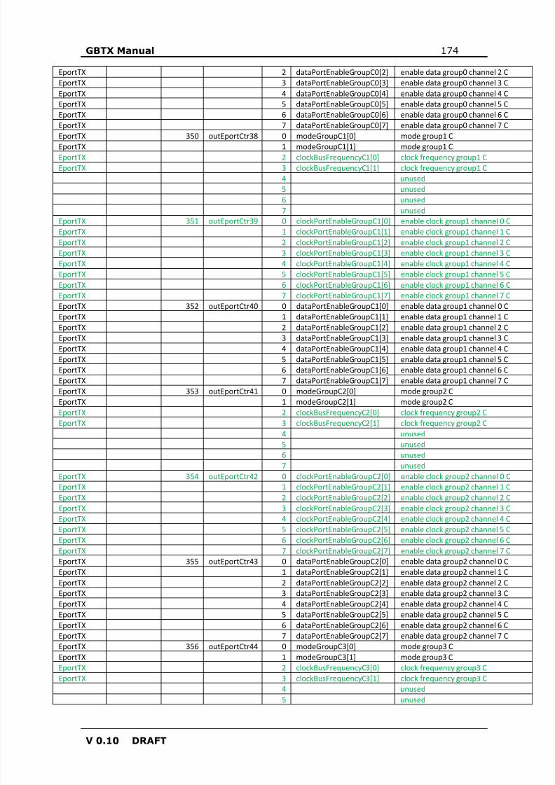
8/15/2019 gbtx Manual
http://slidepdf.com/reader/full/gbtx-manual 174/200
GBTX Manual 174
V 0.10 DRAFT
EportTX 2 dataPortEnableGroupC0[2] enable data group0 channel 2 CEportTX 3 dataPortEnableGroupC0[3] enable data group0 channel 3 CEportTX 4 dataPortEnableGroupC0[4] enable data group0 channel 4 CEportTX 5 dataPortEnableGroupC0[5] enable data group0 channel 5 CEportTX 6 dataPortEnableGroupC0[6] enable data group0 channel 6 CEportTX 7 dataPortEnableGroupC0[7] enable data group0 channel 7 C
EportTX 350 outEportCtr38 0 modeGroupC1[0] mode group1 CEportTX 1 modeGroupC1[1] mode group1 CEportTX 2 clockBusFrequencyC1[0] clock frequency group1 CEportTX 3 clockBusFrequencyC1[1] clock frequency group1 C
4 unused5 unused6 unused7 unused
EportTX 351 outEportCtr39 0 clockPortEnableGroupC1[0] enable clock group1 channel 0 CEportTX 1 clockPortEnableGroupC1[1] enable clock group1 channel 1 CEportTX 2 clockPortEnableGroupC1[2] enable clock group1 channel 2 CEportTX 3 clockPortEnableGroupC1[3] enable clock group1 channel 3 CEportTX 4 clockPortEnableGroupC1[4] enable clock group1 channel 4 C
EportTX 5 clockPortEnableGroupC1[5] enable clock group1 channel 5 CEportTX 6 clockPortEnableGroupC1[6] enable clock group1 channel 6 CEportTX 7 clockPortEnableGroupC1[7] enable clock group1 channel 7 CEportTX 352 outEportCtr40 0 dataPortEnableGroupC1[0] enable data group1 channel 0 CEportTX 1 dataPortEnableGroupC1[1] enable data group1 channel 1 CEportTX 2 dataPortEnableGroupC1[2] enable data group1 channel 2 CEportTX 3 dataPortEnableGroupC1[3] enable data group1 channel 3 CEportTX 4 dataPortEnableGroupC1[4] enable data group1 channel 4 CEportTX 5 dataPortEnableGroupC1[5] enable data group1 channel 5 CEportTX 6 dataPortEnableGroupC1[6] enable data group1 channel 6 CEportTX 7 dataPortEnableGroupC1[7] enable data group1 channel 7 CEportTX 353 outEportCtr41 0 modeGroupC2[0] mode group2 CEportTX 1 modeGroupC2[1] mode group2 C
EportTX 2 clockBusFrequencyC2[0] clock frequency group2 CEportTX 3 clockBusFrequencyC2[1] clock frequency group2 C
4 unused5 unused6 unused7 unused
EportTX 354 outEportCtr42 0 clockPortEnableGroupC2[0] enable clock group2 channel 0 CEportTX 1 clockPortEnableGroupC2[1] enable clock group2 channel 1 CEportTX 2 clockPortEnableGroupC2[2] enable clock group2 channel 2 CEportTX 3 clockPortEnableGroupC2[3] enable clock group2 channel 3 CEportTX 4 clockPortEnableGroupC2[4] enable clock group2 channel 4 CEportTX 5 clockPortEnableGroupC2[5] enable clock group2 channel 5 CEportTX 6 clockPortEnableGroupC2[6] enable clock group2 channel 6 C
EportTX 7 clockPortEnableGroupC2[7] enable clock group2 channel 7 CEportTX 355 outEportCtr43 0 dataPortEnableGroupC2[0] enable data group2 channel 0 CEportTX 1 dataPortEnableGroupC2[1] enable data group2 channel 1 CEportTX 2 dataPortEnableGroupC2[2] enable data group2 channel 2 CEportTX 3 dataPortEnableGroupC2[3] enable data group2 channel 3 CEportTX 4 dataPortEnableGroupC2[4] enable data group2 channel 4 CEportTX 5 dataPortEnableGroupC2[5] enable data group2 channel 5 CEportTX 6 dataPortEnableGroupC2[6] enable data group2 channel 6 CEportTX 7 dataPortEnableGroupC2[7] enable data group2 channel 7 CEportTX 356 outEportCtr44 0 modeGroupC3[0] mode group3 CEportTX 1 modeGroupC3[1] mode group3 CEportTX 2 clockBusFrequencyC3[0] clock frequency group3 CEportTX 3 clockBusFrequencyC3[1] clock frequency group3 C
4 unused5 unused
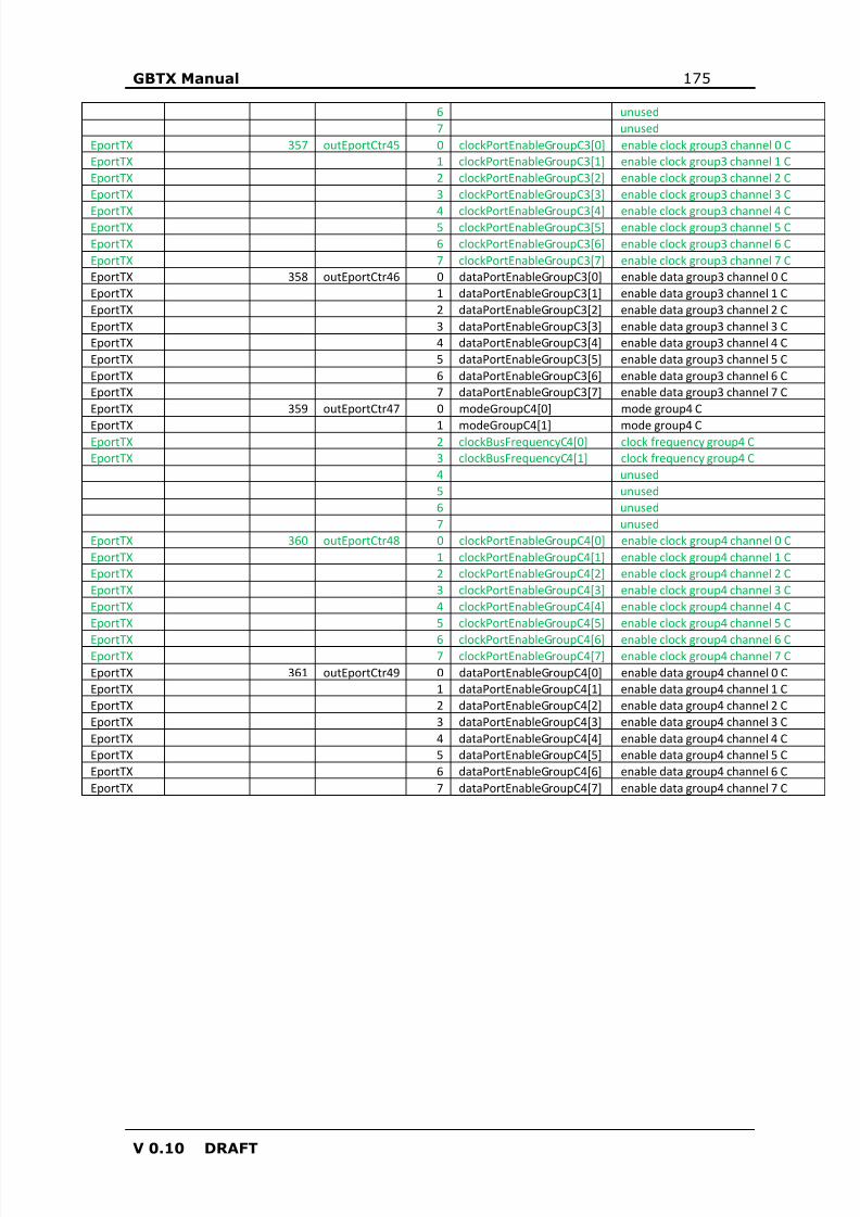
8/15/2019 gbtx Manual
http://slidepdf.com/reader/full/gbtx-manual 175/200
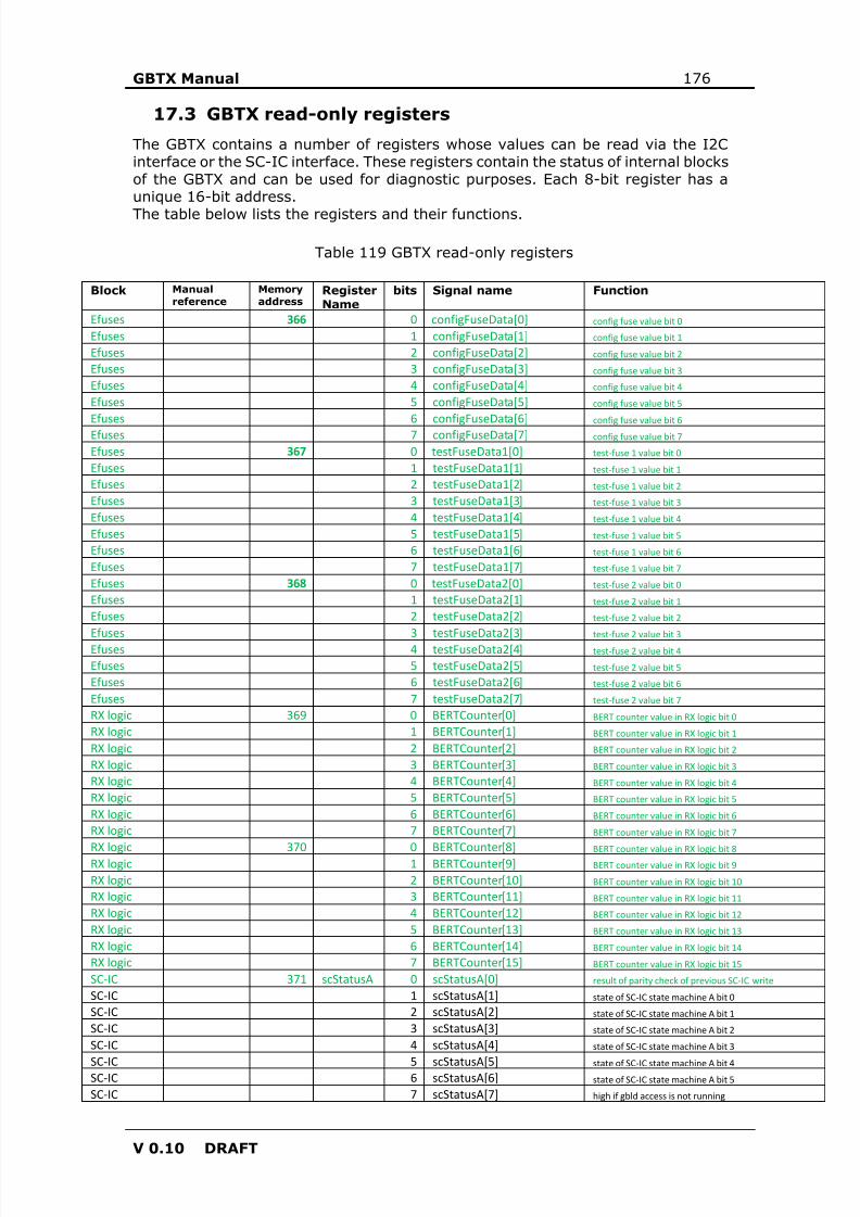
8/15/2019 gbtx Manual
http://slidepdf.com/reader/full/gbtx-manual 176/200
GBTX Manual 176
V 0.10 DRAFT
17.3 GBTX read-only registers
The GBTX contains a number of registers whose values can be read via the I2Cinterface or the SC-IC interface. These registers contain the status of internal blocksof the GBTX and can be used for diagnostic purposes. Each 8-bit register has aunique 16-bit address.The table below lists the registers and their functions.
Table 119 GBTX read-only registers
Block Manualreference
Memoryaddress
RegisterName
bits Signal name Function
Efuses 366 0 configFuseData[0] config fuse value bit 0
Efuses 1 configFuseData[1] config fuse value bit 1
Efuses 2 configFuseData[2] config fuse value bit 2
Efuses 3 configFuseData[3] config fuse value bit 3
Efuses 4 configFuseData[4] config fuse value bit 4
Efuses 5 configFuseData[5] config fuse value bit 5
Efuses 6 configFuseData[6] config fuse value bit 6
Efuses 7 configFuseData[7] config fuse value bit 7
Efuses 367 0 testFuseData1[0] test-fuse 1 value bit 0
Efuses 1 testFuseData1[1] test-fuse 1 value bit 1
Efuses 2 testFuseData1[2] test-fuse 1 value bit 2
Efuses 3 testFuseData1[3] test-fuse 1 value bit 3
Efuses 4 testFuseData1[4] test-fuse 1 value bit 4
Efuses 5 testFuseData1[5] test-fuse 1 value bit 5
Efuses 6 testFuseData1[6] test-fuse 1 value bit 6
Efuses 7 testFuseData1[7] test-fuse 1 value bit 7
Efuses 368 0 testFuseData2[0] test-fuse 2 value bit 0
Efuses 1 testFuseData2[1] test-fuse 2 value bit 1
Efuses 2 testFuseData2[2] test-fuse 2 value bit 2
Efuses 3 testFuseData2[3] test-fuse 2 value bit 3
Efuses 4 testFuseData2[4] test-fuse 2 value bit 4
Efuses 5 testFuseData2[5] test-fuse 2 value bit 5
Efuses 6 testFuseData2[6] test-fuse 2 value bit 6
Efuses 7 testFuseData2[7] test-fuse 2 value bit 7
RX logic 369 0 BERTCounter[0] BERT counter value in RX logic bit 0
RX logic 1 BERTCounter[1] BERT counter value in RX logic bit 1
RX logic 2 BERTCounter[2] BERT counter value in RX logic bit 2
RX logic 3 BERTCounter[3] BERT counter value in RX logic bit 3
RX logic 4 BERTCounter[4] BERT counter value in RX logic bit 4
RX logic 5 BERTCounter[5] BERT counter value in RX logic bit 5
RX logic 6 BERTCounter[6] BERT counter value in RX logic bit 6
RX logic 7 BERTCounter[7] BERT counter value in RX logic bit 7
RX logic 370 0 BERTCounter[8] BERT counter value in RX logic bit 8RX logic 1 BERTCounter[9] BERT counter value in RX logic bit 9
RX logic 2 BERTCounter[10] BERT counter value in RX logic bit 10
RX logic 3 BERTCounter[11] BERT counter value in RX logic bit 11
RX logic 4 BERTCounter[12] BERT counter value in RX logic bit 12
RX logic 5 BERTCounter[13] BERT counter value in RX logic bit 13
RX logic 6 BERTCounter[14] BERT counter value in RX logic bit 14
RX logic 7 BERTCounter[15] BERT counter value in RX logic bit 15
SC-IC 371 scStatusA 0 scStatusA[0] result of parity check of previous SC-IC write
SC-IC 1 scStatusA[1] state of SC-IC state machine A bit 0
SC-IC 2 scStatusA[2] state of SC-IC state machine A bit 1
SC-IC 3 scStatusA[3] state of SC-IC state machine A bit 2
SC-IC 4 scStatusA[4] state of SC-IC state machine A bit 3
SC-IC 5 scStatusA[5] state of SC-IC state machine A bit 4SC-IC 6 scStatusA[6] state of SC-IC state machine A bit 5
SC-IC 7 scStatusA[7] high if gbld access is not running
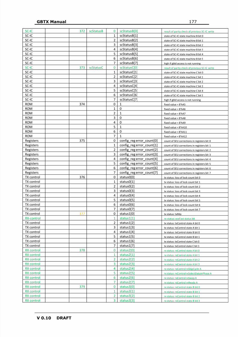
8/15/2019 gbtx Manual
http://slidepdf.com/reader/full/gbtx-manual 177/200
GBTX Manual 177
V 0.10 DRAFT
SC-IC 372 scStatusB 0 scStatusB[0] result of parity check of previous SC-IC write
SC-IC 1 scStatusB[1] state of SC-IC state machine B bit 0
SC-IC 2 scStatusB[2] state of SC-IC state machine B bit 1
SC-IC 3 scStatusB[3] state of SC-IC state machine B bit 2
SC-IC 4 scStatusB[4] state of SC-IC state machine B bit 3
SC-IC 5 scStatusB[5] state of SC-IC state machine B bit 4
SC-IC 6 scStatusB[6] state of SC-IC state machine B bit 5SC-IC 7 scStatusB[7] high if gbld access is not running
SC-IC 373 scStatusC 0 scStatusC[0] result of parity check of previous SC-IC write
SC-IC 1 scStatusC[1] state of SC-IC state machine C bit 0
SC-IC 2 scStatusC[2] state of SC-IC state machine C bit 1
SC-IC 3 scStatusC[3] state of SC-IC state machine C bit 2
SC-IC 4 scStatusC[4] state of SC-IC state machine C bit 3
SC-IC 5 scStatusC[5] state of SC-IC state machine C bit 4
SC-IC 6 scStatusC[6] state of SC-IC state machine C bit 5
SC-IC 7 scStatusC[7] high if gbld access is not running
ROM 374 0 1 fixed value = 8'hA5
ROM 1 0 fixed value = 8'hA6
ROM 2 1 fixed value = 8'hA7
ROM 3 0 fixed value = 8'hA8ROM 4 0 fixed value = 8'hA9
ROM 5 1 fixed value = 8'hA10
ROM 6 0 fixed value = 8'hA11
ROM 7 1 fixed value = 8'hA12
Registers 375 0 config_reg error_count[0] count of SEU corrections in registers bit 0
Registers 1 config_reg error_count[1] count of SEU corrections in registers bit 1
Registers 2 config_reg error_count[2] count of SEU corrections in registers bit 2
Registers 3 config_reg error_count[3] count of SEU corrections in registers bit 3
Registers 4 config_reg error_count[4] count of SEU corrections in registers bit 4
Registers 5 config_reg error_count[5] count of SEU corrections in registers bit 5
Registers 6 config_reg error_count[6] count of SEU corrections in registers bit 6
Registers 7 config_reg error_count[7] count of SEU corrections in registers bit 7
TX control 376 0 status0[0] tx status: loss of lock count bit 0TX control 1 status0[1] tx status: loss of lock count bit 1
TX control 2 status0[2] tx status: loss of lock count bit 2
TX control 3 status0[3] tx status: loss of lock count bit 3
TX control 4 status0[4] tx status: loss of lock count bit 4
TX control 5 status0[5] tx status: loss of lock count bit 5
TX control 6 status0[6] tx status: loss of lock count bit 6
TX control 7 status0[7] tx status: loss of lock count bit 7
TX control 377 0 status1[0] tx status: txRdy
RX-control 1 status1[1] rx-status: vcoFast status bit
TX control 2 status1[2] tx status: txControl state A bit 0
TX control 3 status1[3] tx status: txControl state A bit 1
TX control 4 status1[4] tx status: txControl state B bit 0
TX control 5 status1[5] tx status: txControl state B bit 1TX control 6 status1[6] tx status: txControl state C bit 0
TX control 7 status1[7] tx status: txControl state C bit 1
RX control 378 0 status2[0] rx status: rxControl state A bit 0
RX control 1 status2[1] rx status: rxControl state A bit 1
RX control 2 status2[2] rx status: rxControl state A bit 2
RX control 3 status2[3] rx status: rxControl state A bit 3
RX control 4 status2[4] rx status: rxControl rxSkipCycle A
RX control 5 status2[5] rx status: rxControl rxSelectDataInPhase A
RX control 6 status2[6] rx status: rxControl rxSwap A
RX control 7 status2[7] rx status: rxControl rxReady A
RX control 379 0 status3[0] rx status: rxControl state B bit 0
RX control 1 status3[1] rx status: rxControl state B bit 1
RX control 2 status3[2] rx status: rxControl state B bit 2
RX control 3 status3[3] rx status: rxControl state B bit 3
8/15/2019 gbtx Manual
http://slidepdf.com/reader/full/gbtx-manual 178/200
GBTX Manual 178
V 0.10 DRAFT
RX control 4 status3[4] rx status: rxControl rxSkipCycle B
RX control 5 status3[5] rx status: rxControl rxSelectDataInPhase B
RX control 6 status3[6] rx status: rxControl rxSwap B
RX control 7 status3[7] rx status: rxControl rxReady B
RX control 380 0 status4[0] rx status: rxControl state C bit 0
RX control 1 status4[1] rx status: rxControl state C bit 1
RX control 2 status4[2] rx status: rxControl state C bit 2RX control 3 status4[3] rx status: rxControl state C bit 3
RX control 4 status4[4] rx status: rxControl rxSkipCycle C
RX control 5 status4[5] rx status: rxControl rxSelectDataInPhase C
RX control 6 status4[6] rx status: rxControl rxSwap C
RX control 7 status4[7] rx status: rxControl rxReady C
GBLD access 381 0 gbld_r0[0] GBLD read data, register0, bit 0
GBLD access 1 gbld_r0[1] GBLD read data, register0, bit 1
GBLD access 2 gbld_r0[2] GBLD read data, register0, bit 2
GBLD access 3 gbld_r0[3] GBLD read data, register0, bit 3
GBLD access 4 gbld_r0[4] GBLD read data, register0, bit 4
GBLD access 5 gbld_r0[5] GBLD read data, register0, bit 5
GBLD access 6 gbld_r0[6] GBLD read data, register0, bit 6
GBLD access 7 gbld_r0[7] GBLD read data, register0, bit 7GBLD access 382 0 gbld_r1[0] GBLD read data, register1, bit 0
GBLD access 1 gbld_r1[1] GBLD read data, register1, bit 1
GBLD access 2 gbld_r1[2] GBLD read data, register1, bit 2
GBLD access 3 gbld_r1[3] GBLD read data, register1, bit 3
GBLD access 4 gbld_r1[4] GBLD read data, register1, bit 4
GBLD access 5 gbld_r1[5] GBLD read data, register1, bit 5
GBLD access 6 gbld_r1[6] GBLD read data, register1, bit 6
GBLD access 7 gbld_r1[7] GBLD read data, register1, bit 7
GBLD access 383 0 gbld_r2[0] GBLD read data, register2, bit 0
GBLD access 1 gbld_r2[1] GBLD read data, register2, bit 1
GBLD access 2 gbld_r2[2] GBLD read data, register2, bit 2
GBLD access 3 gbld_r2[3] GBLD read data, register2, bit 3
GBLD access 4 gbld_r2[4] GBLD read data, register2, bit 4GBLD access 5 gbld_r2[5] GBLD read data, register2, bit 5
GBLD access 6 gbld_r2[6] GBLD read data, register2, bit 6
GBLD access 7 gbld_r2[7] GBLD read data, register2, bit 7
GBLD access 384 0 gbld_r3[0] GBLD read data, register3, bit 0
GBLD access 1 gbld_r3[1] GBLD read data, register3, bit 1
GBLD access 2 gbld_r3[2] GBLD read data, register3, bit 2
GBLD access 3 gbld_r3[3] GBLD read data, register3, bit 3
GBLD access 4 gbld_r3[4] GBLD read data, register3, bit 4
GBLD access 5 gbld_r3[5] GBLD read data, register3, bit 5
GBLD access 6 gbld_r3[6] GBLD read data, register3, bit 6
GBLD access 7 gbld_r3[7] GBLD read data, register3, bit 7
GBLD access 385 0 gbld_r4[0] GBLD read data, register4, bit 0
GBLD access 1 gbld_r4[1] GBLD read data, register4, bit 1GBLD access 2 gbld_r4[2] GBLD read data, register4, bit 2
GBLD access 3 gbld_r4[3] GBLD read data, register4, bit 3
GBLD access 4 gbld_r4[4] GBLD read data, register4, bit 4
GBLD access 5 gbld_r4[5] GBLD read data, register4, bit 5
GBLD access 6 gbld_r4[6] GBLD read data, register4, bit 6
GBLD access 7 gbld_r4[7] GBLD read data, register4, bit 7
GBLD access 386 0 gbld_r5[0] GBLD read data, register5, bit 0
GBLD access 1 gbld_r5[1] GBLD read data, register5, bit 1
GBLD access 2 gbld_r5[2] GBLD read data, register5, bit 2
GBLD access 3 gbld_r5[3] GBLD read data, register5, bit 3
GBLD access 4 gbld_r5[4] GBLD read data, register5, bit 4
GBLD access 5 gbld_r5[5] GBLD read data, register5, bit 5
GBLD access 6 gbld_r5[6] GBLD read data, register5, bit 6
GBLD access 7 gbld_r5[7] GBLD read data, register5, bit 7
8/15/2019 gbtx Manual
http://slidepdf.com/reader/full/gbtx-manual 179/200
GBTX Manual 179
V 0.10 DRAFT
GBLD access 387 0 gbld_r6[0] GBLD read data, register6, bit 0
GBLD access 1 gbld_r6[1] GBLD read data, register6, bit 1
GBLD access 2 gbld_r6[2] GBLD read data, register6, bit 2
GBLD access 3 gbld_r6[3] GBLD read data, register6, bit 3
GBLD access 4 gbld_r6[4] GBLD read data, register6, bit 4
GBLD access 5 gbld_r6[5] GBLD read data, register6, bit 5
GBLD access 6 gbld_r6[6] GBLD read data, register6, bit 6GBLD access 7 gbld_r6[7] GBLD read data, register6, bit 7
EportRX 390 0 dllLockedGroup0 EportRX dll locked status, group 0
EportRX 1 dllLockedGroup1 EportRX dll locked status, group 1
EportRX 2 dllLockedGroup2 EportRX dll locked status, group 2
EportRX 3 dllLockedGroup3 EportRX dll locked status, group 3
EportRX 4 dllLockedGroup4 EportRX dll locked status, group 4
EportRX 5 dllLockedGroup5 EportRX dll locked status, group 5
EportRX 6 dllLockedGroup EportRX dll locked status, group 6
EportRX 7 dllLockedEc EportRX dll locked status, EC channel
EportRX 391 0 channelLockedGroup0[0] EportRX phase aligner locked status, group0 ch 0
EportRX 1 channelLockedGroup0[1] EportRX phase aligner locked status, group0 ch 1
EportRX 2 channelLockedGroup0[2] EportRX phase aligner locked status, group0 ch 2
EportRX 3 channelLockedGroup0[3] EportRX phase aligner locked status, group0 ch 3EportRX 4 channelLockedGroup0[4] EportRX phase aligner locked status, group0 ch 4
EportRX 5 channelLockedGroup0[5] EportRX phase aligner locked status, group0 ch 5
EportRX 6 channelLockedGroup0[6] EportRX phase aligner locked status, group0 ch 6
EportRX 7 channelLockedGroup0[7] EportRX phase aligner locked status, group0 ch 7
EportRX 392 0 channelLockedGroup1[0] EportRX phase aligner locked status, group1 ch 0
EportRX 1 channelLockedGroup1[1] EportRX phase aligner locked status, group1 ch 1
EportRX 2 channelLockedGroup1[2] EportRX phase aligner locked status, group1 ch 2
EportRX 3 channelLockedGroup1[3] EportRX phase aligner locked status, group1 ch 3
EportRX 4 channelLockedGroup1[4] EportRX phase aligner locked status, group1 ch 4
EportRX 5 channelLockedGroup1[5] EportRX phase aligner locked status, group1 ch 5
EportRX 6 channelLockedGroup1[6] EportRX phase aligner locked status, group1 ch 6
EportRX 7 channelLockedGroup1[7] EportRX phase aligner locked status, group1 ch 7
EportRX 393 0 channelLockedGroup2[0] EportRX phase aligner locked status, group2 ch 0EportRX 1 channelLockedGroup2[1] EportRX phase aligner locked status, group2 ch 1
EportRX 2 channelLockedGroup2[2] EportRX phase aligner locked status, group2 ch 2
EportRX 3 channelLockedGroup2[3] EportRX phase aligner locked status, group2 ch 3
EportRX 4 channelLockedGroup2[4] EportRX phase aligner locked status, group2 ch 4
EportRX 5 channelLockedGroup2[5] EportRX phase aligner locked status, group2 ch 5
EportRX 6 channelLockedGroup2[6] EportRX phase aligner locked status, group2 ch 6
EportRX 7 channelLockedGroup2[7] EportRX phase aligner locked status, group2 ch 7
EportRX 394 0 channelLockedGroup3[0] EportRX phase aligner locked status, group3 ch 0
EportRX 1 channelLockedGroup3[1] EportRX phase aligner locked status, group3 ch 1
EportRX 2 channelLockedGroup3[2] EportRX phase aligner locked status, group3 ch 2
EportRX 3 channelLockedGroup3[3] EportRX phase aligner locked status, group3 ch 3
EportRX 4 channelLockedGroup3[4] EportRX phase aligner locked status, group3 ch 4
EportRX 5 channelLockedGroup3[5] EportRX phase aligner locked status, group3 ch 5EportRX 6 channelLockedGroup3[6] EportRX phase aligner locked status, group3 ch 6
EportRX 7 channelLockedGroup3[7] EportRX phase aligner locked status, group3 ch 7
EportRX 395 0 channelLockedGroup4[0] EportRX phase aligner locked status, group4 ch 0
EportRX 1 channelLockedGroup4[1] EportRX phase aligner locked status, group4 ch 1
EportRX 2 channelLockedGroup4[2] EportRX phase aligner locked status, group4 ch 2
EportRX 3 channelLockedGroup4[3] EportRX phase aligner locked status, group4 ch 3
EportRX 4 channelLockedGroup4[4] EportRX phase aligner locked status, group4 ch 4
EportRX 5 channelLockedGroup4[5] EportRX phase aligner locked status, group4 ch 5
EportRX 6 channelLockedGroup4[6] EportRX phase aligner locked status, group4 ch 6
EportRX 7 channelLockedGroup4[7] EportRX phase aligner locked status, group4 ch 7
EportRX 396 0 channelLockedGroup5[0] EportRX phase aligner locked status, group5 ch 0
EportRX 1 channelLockedGroup5[1] EportRX phase aligner locked status, group5 ch 1
EportRX 2 channelLockedGroup5[2] EportRX phase aligner locked status, group5 ch 2
EportRX 3 channelLockedGroup5[3] EportRX phase aligner locked status, group5 ch 3
8/15/2019 gbtx Manual
http://slidepdf.com/reader/full/gbtx-manual 180/200
GBTX Manual 180
V 0.10 DRAFT
EportRX 4 channelLockedGroup5[4] EportRX phase aligner locked status, group5 ch 4
EportRX 5 channelLockedGroup5[5] EportRX phase aligner locked status, group5 ch 5
EportRX 6 channelLockedGroup5[6] EportRX phase aligner locked status, group5 ch 6
EportRX 7 channelLockedGroup5[7] EportRX phase aligner locked status, group5 ch 7
EportRX 397 0 channelLockedGroup6[0] EportRX phase aligner locked status, group6 ch 0
EportRX 1 channelLockedGroup6[1] EportRX phase aligner locked status, group6 ch 1
EportRX 2 channelLockedGroup6[2] EportRX phase aligner locked status, group6 ch 2EportRX 3 channelLockedGroup6[3] EportRX phase aligner locked status, group6 ch 3
EportRX 4 channelLockedGroup6[4] EportRX phase aligner locked status, group6 ch 4
EportRX 5 channelLockedGroup6[5] EportRX phase aligner locked status, group6 ch 5
EportRX 6 channelLockedGroup6[6] EportRX phase aligner locked status, group6 ch 6
EportRX 7 channelLockedGroup6[7] EportRX phase aligner locked status, group6 ch 7
EportRX 398 0 phaseSelectOutEc[0] EportRX selected phase EC channel bit 0
EportRX 1 phaseSelectOutEc[1] EportRX selected phase EC channel bit 1
EportRX 2 phaseSelectOutEc[2] EportRX selected phase EC channel bit 2
EportRX 3 phaseSelectOutEc[3] EportRX selected phase EC channel bit 3
EportRX 4 channelLockedGroupEc EportRX phase aligner locked status, EC channel
Unused 5 unused
Unused 6 unused
Unused 7 unusedEportRX 399 0 phaseSelectOutGroup0[0] EportRX selected phase, group0, ch0, bit 0
EportRX 1 phaseSelectOutGroup0[1] EportRX selected phase, group0, ch0, bit 1
EportRX 2 phaseSelectOutGroup0[2] EportRX selected phase, group0, ch0, bit 2
EportRX 3 phaseSelectOutGroup0[3] EportRX selected phase, group0, ch0, bit 3
EportRX 4 phaseSelectOutGroup0[4] EportRX selected phase, group0, ch1, bit 0
EportRX 5 phaseSelectOutGroup0[5] EportRX selected phase, group0, ch1, bit 1
EportRX 6 phaseSelectOutGroup0[6] EportRX selected phase, group0, ch1, bit 2
EportRX 7 phaseSelectOutGroup0[7] EportRX selected phase, group0, ch1, bit 3
EportRX 400 0 phaseSelectOutGroup0[8] EportRX selected phase, group0, ch2, bit 0
EportRX 1 phaseSelectOutGroup0[9] EportRX selected phase, group0, ch2, bit 1
EportRX 2 phaseSelectOutGroup0[10] EportRX selected phase, group0, ch2, bit 2
EportRX 3 phaseSelectOutGroup0[11] EportRX selected phase, group0, ch2, bit 3
EportRX 4 phaseSelectOutGroup0[12] EportRX selected phase, group0, ch3, bit 0EportRX 5 phaseSelectOutGroup0[13] EportRX selected phase, group0, ch3, bit 1
EportRX 6 phaseSelectOutGroup0[14] EportRX selected phase, group0, ch3, bit 2
EportRX 7 phaseSelectOutGroup0[15] EportRX selected phase, group0, ch3, bit 3
EportRX 401 0 phaseSelectOutGroup0[16] EportRX selected phase, group0, ch4, bit 0
EportRX 1 phaseSelectOutGroup0[17] EportRX selected phase, group0, ch4, bit 1
EportRX 2 phaseSelectOutGroup0[18] EportRX selected phase, group0, ch4, bit 2
EportRX 3 phaseSelectOutGroup0[19] EportRX selected phase, group0, ch4, bit 3
EportRX 4 phaseSelectOutGroup0[20] EportRX selected phase, group0, ch5, bit 0
EportRX 5 phaseSelectOutGroup0[21] EportRX selected phase, group0, ch5, bit 1
EportRX 6 phaseSelectOutGroup0[22] EportRX selected phase, group0, ch5, bit 2
EportRX 7 phaseSelectOutGroup0[23] EportRX selected phase, group0, ch5, bit 3
EportRX 402 0 phaseSelectOutGroup0[24] EportRX selected phase, group0, ch6, bit 0
EportRX 1 phaseSelectOutGroup0[25] EportRX selected phase, group0, ch6, bit 1EportRX 2 phaseSelectOutGroup0[26] EportRX selected phase, group0, ch6, bit 2
EportRX 3 phaseSelectOutGroup0[27] EportRX selected phase, group0, ch6, bit 3
EportRX 4 phaseSelectOutGroup0[28] EportRX selected phase, group0, ch7, bit 0
EportRX 5 phaseSelectOutGroup0[29] EportRX selected phase, group0, ch7, bit 1
EportRX 6 phaseSelectOutGroup0[30] EportRX selected phase, group0, ch7, bit 2
EportRX 7 phaseSelectOutGroup0[31] EportRX selected phase, group0, ch7, bit 3
EportRX 403 0 phaseSelectOutGroup1[0] EportRX selected phase, group1, ch0, bit 0
EportRX 1 phaseSelectOutGroup1[1] EportRX selected phase, group1, ch0, bit 1
EportRX 2 phaseSelectOutGroup1[2] EportRX selected phase, group1, ch0, bit 2
EportRX 3 phaseSelectOutGroup1[3] EportRX selected phase, group1, ch0, bit 3
EportRX 4 phaseSelectOutGroup1[4] EportRX selected phase, group1, ch1, bit 0
EportRX 5 phaseSelectOutGroup1[5] EportRX selected phase, group1, ch1, bit 1
EportRX 6 phaseSelectOutGroup1[6] EportRX selected phase, group1, ch1, bit 2
EportRX 7 phaseSelectOutGroup1[7] EportRX selected phase, group1, ch1, bit 3
8/15/2019 gbtx Manual
http://slidepdf.com/reader/full/gbtx-manual 181/200
GBTX Manual 181
V 0.10 DRAFT
EportRX 404 0 phaseSelectOutGroup1[8] EportRX selected phase, group1, ch2, bit 0
EportRX 1 phaseSelectOutGroup1[9] EportRX selected phase, group1, ch2, bit 1
EportRX 2 phaseSelectOutGroup1[10] EportRX selected phase, group1, ch2, bit 2
EportRX 3 phaseSelectOutGroup1[11] EportRX selected phase, group1, ch2, bit 3
EportRX 4 phaseSelectOutGroup1[12] EportRX selected phase, group1, ch3, bit 0
EportRX 5 phaseSelectOutGroup1[13] EportRX selected phase, group1, ch3, bit 1
EportRX 6 phaseSelectOutGroup1[14] EportRX selected phase, group1, ch3, bit 2EportRX 7 phaseSelectOutGroup1[15] EportRX selected phase, group1, ch3, bit 3
EportRX 405 0 phaseSelectOutGroup1[16] EportRX selected phase, group1, ch4, bit 0
EportRX 1 phaseSelectOutGroup1[17] EportRX selected phase, group1, ch4, bit 1
EportRX 2 phaseSelectOutGroup1[18] EportRX selected phase, group1, ch4, bit 2
EportRX 3 phaseSelectOutGroup1[19] EportRX selected phase, group1, ch4, bit 3
EportRX 4 phaseSelectOutGroup1[20] EportRX selected phase, group1, ch5, bit 0
EportRX 5 phaseSelectOutGroup1[21] EportRX selected phase, group1, ch5, bit 1
EportRX 6 phaseSelectOutGroup1[22] EportRX selected phase, group1, ch5, bit 2
EportRX 7 phaseSelectOutGroup1[23] EportRX selected phase, group1, ch5, bit 3
EportRX 406 0 phaseSelectOutGroup1[24] EportRX selected phase, group1, ch6, bit 0
EportRX 1 phaseSelectOutGroup1[25] EportRX selected phase, group1, ch6, bit 1
EportRX 2 phaseSelectOutGroup1[26] EportRX selected phase, group1, ch6, bit 2
EportRX 3 phaseSelectOutGroup1[27] EportRX selected phase, group1, ch6, bit 3EportRX 4 phaseSelectOutGroup1[28] EportRX selected phase, group1, ch7, bit 0
EportRX 5 phaseSelectOutGroup1[29] EportRX selected phase, group1, ch7, bit 1
EportRX 6 phaseSelectOutGroup1[30] EportRX selected phase, group1, ch7, bit 2
EportRX 7 phaseSelectOutGroup1[31] EportRX selected phase, group1, ch7, bit 3
EportRX 407 0 phaseSelectOutGroup2[0] EportRX selected phase, group2, ch0, bit 0
EportRX 1 phaseSelectOutGroup2[1] EportRX selected phase, group2, ch0, bit 1
EportRX 2 phaseSelectOutGroup2[2] EportRX selected phase, group2, ch0, bit 2
EportRX 3 phaseSelectOutGroup2[3] EportRX selected phase, group2, ch0, bit 3
EportRX 4 phaseSelectOutGroup2[4] EportRX selected phase, group2, ch1, bit 0
EportRX 5 phaseSelectOutGroup2[5] EportRX selected phase, group2, ch1, bit 1
EportRX 6 phaseSelectOutGroup2[6] EportRX selected phase, group2, ch1, bit 2
EportRX 7 phaseSelectOutGroup2[7] EportRX selected phase, group2, ch1, bit 3
EportRX 408 0 phaseSelectOutGroup2[8] EportRX selected phase, group2, ch2, bit 0EportRX 1 phaseSelectOutGroup2[9] EportRX selected phase, group2, ch2, bit 1
EportRX 2 phaseSelectOutGroup2[10] EportRX selected phase, group2, ch2, bit 2
EportRX 3 phaseSelectOutGroup2[11] EportRX selected phase, group2, ch2, bit 3
EportRX 4 phaseSelectOutGroup2[12] EportRX selected phase, group2, ch3, bit 0
EportRX 5 phaseSelectOutGroup2[13] EportRX selected phase, group2, ch3, bit 1
EportRX 6 phaseSelectOutGroup2[14] EportRX selected phase, group2, ch3, bit 2
EportRX 7 phaseSelectOutGroup2[15] EportRX selected phase, group2, ch3, bit 3
EportRX 409 0 phaseSelectOutGroup2[16] EportRX selected phase, group2, ch4, bit 0
EportRX 1 phaseSelectOutGroup2[17] EportRX selected phase, group2, ch4, bit 1
EportRX 2 phaseSelectOutGroup2[18] EportRX selected phase, group2, ch4, bit 2
EportRX 3 phaseSelectOutGroup2[19] EportRX selected phase, group2, ch4, bit 3
EportRX 4 phaseSelectOutGroup2[20] EportRX selected phase, group2, ch5, bit 0
EportRX 5 phaseSelectOutGroup2[21] EportRX selected phase, group2, ch5, bit 1EportRX 6 phaseSelectOutGroup2[22] EportRX selected phase, group2, ch5, bit 2
EportRX 7 phaseSelectOutGroup2[23] EportRX selected phase, group2, ch5, bit 3
EportRX 410 0 phaseSelectOutGroup2[24] EportRX selected phase, group2, ch6, bit 0
EportRX 1 phaseSelectOutGroup2[25] EportRX selected phase, group2, ch6, bit 1
EportRX 2 phaseSelectOutGroup2[26] EportRX selected phase, group2, ch6, bit 2
EportRX 3 phaseSelectOutGroup2[27] EportRX selected phase, group2, ch6, bit 3
EportRX 4 phaseSelectOutGroup2[28] EportRX selected phase, group2, ch7, bit 0
EportRX 5 phaseSelectOutGroup2[29] EportRX selected phase, group2, ch7, bit 1
EportRX 6 phaseSelectOutGroup2[30] EportRX selected phase, group2, ch7, bit 2
EportRX 7 phaseSelectOutGroup2[31] EportRX selected phase, group2, ch7, bit 3
EportRX 411 0 phaseSelectOutGroup3[0] EportRX selected phase, group3, ch0, bit 0
EportRX 1 phaseSelectOutGroup3[1] EportRX selected phase, group3, ch0, bit 1
EportRX 2 phaseSelectOutGroup3[2] EportRX selected phase, group3, ch0, bit 2
EportRX 3 phaseSelectOutGroup3[3] EportRX selected phase, group3, ch0, bit 3
8/15/2019 gbtx Manual
http://slidepdf.com/reader/full/gbtx-manual 182/200
GBTX Manual 182
V 0.10 DRAFT
EportRX 4 phaseSelectOutGroup3[4] EportRX selected phase, group3, ch1, bit 0
EportRX 5 phaseSelectOutGroup3[5] EportRX selected phase, group3, ch1, bit 1
EportRX 6 phaseSelectOutGroup3[6] EportRX selected phase, group3, ch1, bit 2
EportRX 7 phaseSelectOutGroup3[7] EportRX selected phase, group3, ch1, bit 3
EportRX 412 0 phaseSelectOutGroup3[8] EportRX selected phase, group3, ch2, bit 0
EportRX 1 phaseSelectOutGroup3[9] EportRX selected phase, group3, ch2, bit 1
EportRX 2 phaseSelectOutGroup3[10] EportRX selected phase, group3, ch2, bit 2EportRX 3 phaseSelectOutGroup3[11] EportRX selected phase, group3, ch2, bit 3
EportRX 4 phaseSelectOutGroup3[12] EportRX selected phase, group3, ch3, bit 0
EportRX 5 phaseSelectOutGroup3[13] EportRX selected phase, group3, ch3, bit 1
EportRX 6 phaseSelectOutGroup3[14] EportRX selected phase, group3, ch3, bit 2
EportRX 7 phaseSelectOutGroup3[15] EportRX selected phase, group3, ch3, bit 3
EportRX 413 0 phaseSelectOutGroup3[16] EportRX selected phase, group3, ch4, bit 0
EportRX 1 phaseSelectOutGroup3[17] EportRX selected phase, group3, ch4, bit 1
EportRX 2 phaseSelectOutGroup3[18] EportRX selected phase, group3, ch4, bit 2
EportRX 3 phaseSelectOutGroup3[19] EportRX selected phase, group3, ch4, bit 3
EportRX 4 phaseSelectOutGroup3[20] EportRX selected phase, group3, ch5, bit 0
EportRX 5 phaseSelectOutGroup3[21] EportRX selected phase, group3, ch5, bit 1
EportRX 6 phaseSelectOutGroup3[22] EportRX selected phase, group3, ch5, bit 2
EportRX 7 phaseSelectOutGroup3[23] EportRX selected phase, group3, ch5, bit 3EportRX 414 0 phaseSelectOutGroup3[24] EportRX selected phase, group3, ch6, bit 0
EportRX 1 phaseSelectOutGroup3[25] EportRX selected phase, group3, ch6, bit 1
EportRX 2 phaseSelectOutGroup3[26] EportRX selected phase, group3, ch6, bit 2
EportRX 3 phaseSelectOutGroup3[27] EportRX selected phase, group3, ch6, bit 3
EportRX 4 phaseSelectOutGroup3[28] EportRX selected phase, group3, ch7, bit 0
EportRX 5 phaseSelectOutGroup3[29] EportRX selected phase, group3, ch7, bit 1
EportRX 6 phaseSelectOutGroup3[30] EportRX selected phase, group3, ch7, bit 2
EportRX 7 phaseSelectOutGroup3[31] EportRX selected phase, group3, ch7, bit 3
EportRX 415 0 phaseSelectOutGroup4[0] EportRX selected phase, group4, ch0, bit 0
EportRX 1 phaseSelectOutGroup4[1] EportRX selected phase, group4, ch0, bit 1
EportRX 2 phaseSelectOutGroup4[2] EportRX selected phase, group4, ch0, bit 2
EportRX 3 phaseSelectOutGroup4[3] EportRX selected phase, group4, ch0, bit 3
EportRX 4 phaseSelectOutGroup4[4] EportRX selected phase, group4, ch1, bit 0EportRX 5 phaseSelectOutGroup4[5] EportRX selected phase, group4, ch1, bit 1
EportRX 6 phaseSelectOutGroup4[6] EportRX selected phase, group4, ch1, bit 2
EportRX 7 phaseSelectOutGroup4[7] EportRX selected phase, group4, ch1, bit 3
EportRX 416 0 phaseSelectOutGroup4[8] EportRX selected phase, group4, ch2, bit 0
EportRX 1 phaseSelectOutGroup4[9 EportRX selected phase, group4, ch2, bit 1
EportRX 2 phaseSelectOutGroup4[10] EportRX selected phase, group4, ch2, bit 2
EportRX 3 phaseSelectOutGroup4[11] EportRX selected phase, group4, ch2, bit 3
EportRX 4 phaseSelectOutGroup4[12] EportRX selected phase, group4, ch3, bit 0
EportRX 5 phaseSelectOutGroup4[13] EportRX selected phase, group4, ch3, bit 1
EportRX 6 phaseSelectOutGroup4[14] EportRX selected phase, group4, ch3, bit 2
EportRX 7 phaseSelectOutGroup4[15] EportRX selected phase, group4, ch3, bit 3
EportRX 417 0 phaseSelectOutGroup4[16] EportRX selected phase, group4, ch4, bit 0
EportRX 1 phaseSelectOutGroup4[17] EportRX selected phase, group4, ch4, bit 1EportRX 2 phaseSelectOutGroup4[18] EportRX selected phase, group4, ch4, bit 2
EportRX 3 phaseSelectOutGroup4[19] EportRX selected phase, group4, ch4, bit 3
EportRX 4 phaseSelectOutGroup4[20] EportRX selected phase, group4, ch5, bit 0
EportRX 5 phaseSelectOutGroup4[21] EportRX selected phase, group4, ch5, bit 1
EportRX 6 phaseSelectOutGroup4[22] EportRX selected phase, group4, ch5, bit 2
EportRX 7 phaseSelectOutGroup4[23] EportRX selected phase, group4, ch5, bit 3
EportRX 418 0 phaseSelectOutGroup4[24] EportRX selected phase, group4, ch6, bit 0
EportRX 1 phaseSelectOutGroup4[25] EportRX selected phase, group4, ch6, bit 1
EportRX 2 phaseSelectOutGroup4[26] EportRX selected phase, group4, ch6, bit 2
EportRX 3 phaseSelectOutGroup4[27] EportRX selected phase, group4, ch6, bit 3
EportRX 4 phaseSelectOutGroup4[28] EportRX selected phase, group4, ch7, bit 0
EportRX 5 phaseSelectOutGroup4[29] EportRX selected phase, group4, ch7, bit 1
EportRX 6 phaseSelectOutGroup4[30] EportRX selected phase, group4, ch7, bit 2
EportRX 7 phaseSelectOutGroup4[31] EportRX selected phase, group4, ch7, bit 3
8/15/2019 gbtx Manual
http://slidepdf.com/reader/full/gbtx-manual 183/200
GBTX Manual 183
V 0.10 DRAFT
EportRX 419 0 phaseSelectOutGroup5[0] EportRX selected phase, group5, ch0, bit 0
EportRX 1 phaseSelectOutGroup5[1] EportRX selected phase, group5, ch0, bit 1
EportRX 2 phaseSelectOutGroup5[2] EportRX selected phase, group5, ch0, bit 2
EportRX 3 phaseSelectOutGroup5[3] EportRX selected phase, group5, ch0, bit 3
EportRX 4 phaseSelectOutGroup5[4] EportRX selected phase, group5, ch1, bit 0
EportRX 5 phaseSelectOutGroup5[5] EportRX selected phase, group5, ch1, bit 1
EportRX 6 phaseSelectOutGroup5[6] EportRX selected phase, group5, ch1, bit 2EportRX 7 phaseSelectOutGroup5[7] EportRX selected phase, group5, ch1, bit 3
EportRX 420 0 phaseSelectOutGroup5[8] EportRX selected phase, group5, ch2, bit 0
EportRX 1 phaseSelectOutGroup5[9] EportRX selected phase, group5, ch2, bit 1
EportRX 2 phaseSelectOutGroup5[10] EportRX selected phase, group5, ch2, bit 2
EportRX 3 phaseSelectOutGroup5[11] EportRX selected phase, group5, ch2, bit 3
EportRX 4 phaseSelectOutGroup5[12] EportRX selected phase, group5, ch3, bit 0
EportRX 5 phaseSelectOutGroup5[13] EportRX selected phase, group5, ch3, bit 1
EportRX 6 phaseSelectOutGroup5[14] EportRX selected phase, group5, ch3, bit 2
EportRX 7 phaseSelectOutGroup5[15] EportRX selected phase, group5, ch3, bit 3
EportRX 421 0 phaseSelectOutGroup5[16] EportRX selected phase, group5, ch4, bit 0
EportRX 1 phaseSelectOutGroup5[17] EportRX selected phase, group5, ch4, bit 1
EportRX 2 phaseSelectOutGroup5[18] EportRX selected phase, group5, ch4, bit 2
EportRX 3 phaseSelectOutGroup5[19] EportRX selected phase, group5, ch4, bit 3EportRX 4 phaseSelectOutGroup5[20] EportRX selected phase, group5, ch5, bit 0
EportRX 5 phaseSelectOutGroup5[21] EportRX selected phase, group5, ch5, bit 1
EportRX 6 phaseSelectOutGroup5[22] EportRX selected phase, group5, ch5, bit 2
EportRX 7 phaseSelectOutGroup5[23] EportRX selected phase, group5, ch5, bit 3
EportRX 422 0 phaseSelectOutGroup5[24] EportRX selected phase, group5, ch6, bit 0
EportRX 1 phaseSelectOutGroup5[25] EportRX selected phase, group5, ch6, bit 1
EportRX 2 phaseSelectOutGroup5[26] EportRX selected phase, group5, ch6, bit 2
EportRX 3 phaseSelectOutGroup5[27] EportRX selected phase, group5, ch6, bit 3
EportRX 4 phaseSelectOutGroup5[28] EportRX selected phase, group5, ch7, bit 0
EportRX 5 phaseSelectOutGroup5[29] EportRX selected phase, group5, ch7, bit 1
EportRX 6 phaseSelectOutGroup5[30] EportRX selected phase, group5, ch7, bit 2
EportRX 7 phaseSelectOutGroup5[31] EportRX selected phase, group5, ch7, bit 3
EportRX 423 0 phaseSelectOutGroup6[0] EportRX selected phase, group6, ch0, bit 0EportRX 1 phaseSelectOutGroup6[1] EportRX selected phase, group6, ch0, bit 1
EportRX 2 phaseSelectOutGroup6[2] EportRX selected phase, group6, ch0, bit 2
EportRX 3 phaseSelectOutGroup6[3] EportRX selected phase, group6, ch0, bit 3
EportRX 4 phaseSelectOutGroup6[4] EportRX selected phase, group6, ch1, bit 0
EportRX 5 phaseSelectOutGroup6[5] EportRX selected phase, group6, ch1, bit 1
EportRX 6 phaseSelectOutGroup6[6] EportRX selected phase, group6, ch1, bit 2
EportRX 7 phaseSelectOutGroup6[7] EportRX selected phase, group6, ch1, bit 3
EportRX 424 0 phaseSelectOutGroup6[8] EportRX selected phase, group6, ch2, bit 0
EportRX 1 phaseSelectOutGroup6[9] EportRX selected phase, group6, ch2, bit 1
EportRX 2 phaseSelectOutGroup6[10] EportRX selected phase, group6, ch2, bit 2
EportRX 3 phaseSelectOutGroup6[11] EportRX selected phase, group6, ch2, bit 3
EportRX 4 phaseSelectOutGroup6[12] EportRX selected phase, group6, ch3, bit 0
EportRX 5 phaseSelectOutGroup6[13] EportRX selected phase, group6, ch3, bit 1EportRX 6 phaseSelectOutGroup6[14] EportRX selected phase, group6, ch3, bit 2
EportRX 7 phaseSelectOutGroup6[15] EportRX selected phase, group6, ch3, bit 3
EportRX 425 0 phaseSelectOutGroup6[16] EportRX selected phase, group6, ch4, bit 0
EportRX 1 phaseSelectOutGroup6[17] EportRX selected phase, group6, ch4, bit 1
EportRX 2 phaseSelectOutGroup6[18] EportRX selected phase, group6, ch4, bit 2
EportRX 3 phaseSelectOutGroup6[19] EportRX selected phase, group6, ch4, bit 3
EportRX 4 phaseSelectOutGroup6[20] EportRX selected phase, group6, ch5, bit 0
EportRX 5 phaseSelectOutGroup6[21] EportRX selected phase, group6, ch5, bit 1
EportRX 6 phaseSelectOutGroup6[22] EportRX selected phase, group6, ch5, bit 2
EportRX 7 phaseSelectOutGroup6[23] EportRX selected phase, group6, ch5, bit 3
EportRX 426 0 phaseSelectOutGroup6[24] EportRX selected phase, group6, ch6, bit 0
EportRX 1 phaseSelectOutGroup6[25] EportRX selected phase, group6, ch6, bit 1
EportRX 2 phaseSelectOutGroup6[26] EportRX selected phase, group6, ch6, bit 2
EportRX 3 phaseSelectOutGroup6[27] EportRX selected phase, group6, ch6, bit 3
8/15/2019 gbtx Manual
http://slidepdf.com/reader/full/gbtx-manual 184/200
GBTX Manual 184
V 0.10 DRAFT
EportRX 4 phaseSelectOutGroup6[28] EportRX selected phase, group6, ch7, bit 0
EportRX 5 phaseSelectOutGroup6[29] EportRX selected phase, group6, ch7, bit 1
EportRX 6 phaseSelectOutGroup6[30] EportRX selected phase, group6, ch7, bit 2
EportRX 7 phaseSelectOutGroup6[31] EportRX selected phase, group6, ch7, bit 3
EPLL-TX 427 0 TXEPLLLocked EPLL-TX locked status
TX control 1 txRdy_control txControl txRdy
EPLL-RX 2 RXEPLLLocked EPLL-RX locked statusRX control 3 rxRdy_control rxControl rxRdy
XPLL 4 XPLLLocked XPLL locked status
5 unused
6 unused
7 unusedPhase shifter 428 0 ttcDivideOut phase shifter DivideOutPhase shifter 1 ttcTestDown phase shifter TestDownPhase shifter 2 ttcTestUp phase shifter TestUp
Serialiser 3 txTestUp Serialiser TestUp
Serialiser 4 txTestDown Serialiser TestDown
EPLL-RX 5 ePLLRXInstantLock EPLL-RX instant lock status
EPLL-TX 6 ePLLTXInstantLock EPLL-TX instant lock status
XPLL 7 xPllInstantLock XPLL instant lock statusPhase shifter 429 0 ttcEarly[0] phase shifter Early bit 0Phase shifter 1 ttcEarly[1] phase shifter Early bit 1Phase shifter 2 ttcEarly[2] phase shifter Early bit 2Phase shifter 3 ttcEarly[3] phase shifter Early bit 3Phase shifter 4 ttcEarly[4] phase shifter Early bit 4Phase shifter 5 ttcEarly[5] phase shifter Early bit 5Phase shifter 6 ttcEarly[6] phase shifter Early bit 6Phase shifter 7 ttcEarly[7] phase shifter Early bit 7Phase shifter 430 0 ttcLate[0] phase shifter Late bit 0Phase shifter 1 ttcLate[1] phase shifter Late bit 1Phase shifter 2 ttcLate[2] phase shifter Late bit 2Phase shifter 3 ttcLate[3] phase shifter Late bit 3
Phase shifter 4 ttcLate[4] phase shifter Late bit 4Phase shifter 5 ttcLate[5] phase shifter Late bit 5Phase shifter 6 ttcLate[6] phase shifter Late bit 6Phase shifter 7 ttcLate[7] phase shifter Late bit 7
TX control 431 0 txInstantLockgated Serialiser instant lock status
RX control 1 rxInstantLockRefGated Deserialiser instant lock status
Power-up 2 powerUpFSMState[0] state of powerUp FSM bit 0
Power-up 3 powerUpFSMState[1] state of powerUp FSM bit 1
Power-up 4 powerUpFSMState[2] state of powerUp FSM bit 2
Power-up 5 powerUpFSMState[3] state of powerUp FSM bit 3
Power-up 6 powerUpFSMState[4] state of powerUp FSM bit 4
7 unused
RX control 432 0 rxRefPllLossOfLockCount[0] RF PLL loss of lock count bit 0
RX control 1 rxRefPllLossOfLockCount[1] RF PLL loss of lock count bit 1RX control 2 rxRefPllLossOfLockCount[2] RF PLL loss of lock count bit 2
RX control 3 rxRefPllLossOfLockCount[3] RF PLL loss of lock count bit 3
RX control 4 rxRefPllLossOfLockCount[4] RF PLL loss of lock count bit 4
RX control 5 rxRefPllLossOfLockCount[5] RF PLL loss of lock count bit 5
RX control 6 rxRefPllLossOfLockCount[6] RF PLL loss of lock count bit 6
RX control 7 rxRefPllLossOfLockCount[7] RF PLL loss of lock count bit 7
EPLL-TX 433 0 EPLLTXlossOfLockCount[0] EPLL-TX loss of lock count bit 0
EPLL-TX 1 EPLLTXlossOfLockCount[1] EPLL-TX loss of lock count bit 1
EPLL-TX 2 EPLLTXlossOfLockCount[2] EPLL-TX loss of lock count bit 2
EPLL-TX 3 EPLLTXlossOfLockCount[3] EPLL-TX loss of lock count bit 3
EPLL-TX 4 EPLLTXlossOfLockCount[4] EPLL-TX loss of lock count bit 4
EPLL-TX 5 EPLLTXlossOfLockCount[5] EPLL-TX loss of lock count bit 5
EPLL-TX 6 EPLLTXlossOfLockCount[6] EPLL-TX loss of lock count bit 6
EPLL-TX 7 EPLLTXlossOfLockCount[7] EPLL-TX loss of lock count bit 7
8/15/2019 gbtx Manual
http://slidepdf.com/reader/full/gbtx-manual 185/200
GBTX Manual 185
V 0.10 DRAFT
EPLL-RX 434 0 EPLLRXlossOfLockCount[0] EPLL-RX loss of lock count bit 0
EPLL-RX 1 EPLLRXlossOfLockCount[1] EPLL-RX loss of lock count bit 1
EPLL-RX 2 EPLLRXlossOfLockCount[2] EPLL-RX loss of lock count bit 2
EPLL-RX 3 EPLLRXlossOfLockCount[3] EPLL-RX loss of lock count bit 3
EPLL-RX 4 EPLLRXlossOfLockCount[4] EPLL-RX loss of lock count bit 4
EPLL-RX 5 EPLLRXlossOfLockCount[5] EPLL-RX loss of lock count bit 5
EPLL-RX 6 EPLLRXlossOfLockCount[6] EPLL-RX loss of lock count bit 6EPLL-RX 7 EPLLRXlossOfLockCount[7] EPLL-RX loss of lock count bit 7
RX logic 435 0 FECcorrectionCount[0] Count of FEC corrections in RX, bit 0
RX logic 1 FECcorrectionCount[1] Count of FEC corrections in RX, bit 1
RX logic 2 FECcorrectionCount[2] Count of FEC corrections in RX, bit 2
RX logic 3 FECcorrectionCount[3] Count of FEC corrections in RX, bit 3
RX logic 4 FECcorrectionCount[4] Count of FEC corrections in RX, bit 4
RX logic 5 FECcorrectionCount[5] Count of FEC corrections in RX, bit 5
RX logic 6 FECcorrectionCount[6] Count of FEC corrections in RX, bit 6
RX logic 7 FECcorrectionCount[7] Count of FEC corrections in RX, bit 7

8/15/2019 gbtx Manual
http://slidepdf.com/reader/full/gbtx-manual 186/200
GBTX Manual 186
V 0.10 DRAFT
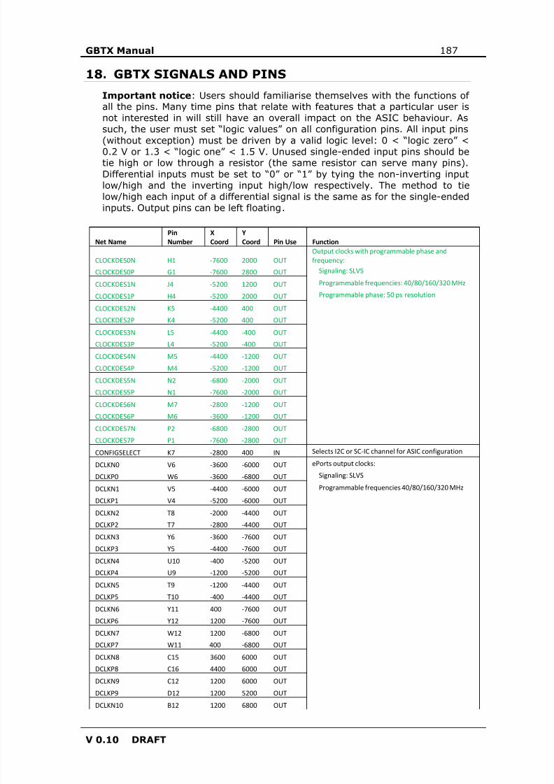
8/15/2019 gbtx Manual
http://slidepdf.com/reader/full/gbtx-manual 187/200
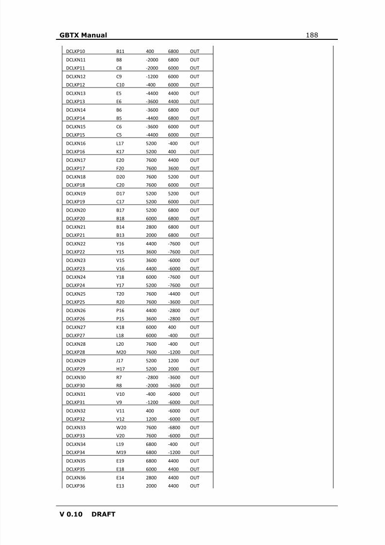
8/15/2019 gbtx Manual
http://slidepdf.com/reader/full/gbtx-manual 188/200
GBTX Manual 188
V 0.10 DRAFT
DCLKP10 B11 400 6800 OUT
DCLKN11 B8 -2000 6800 OUT
DCLKP11 C8 -2000 6000 OUT
DCLKN12 C9 -1200 6000 OUT
DCLKP12 C10 -400 6000 OUT
DCLKN13 E5 -4400 4400 OUTDCLKP13 E6 -3600 4400 OUT
DCLKN14 B6 -3600 6800 OUT
DCLKP14 B5 -4400 6800 OUT
DCLKN15 C6 -3600 6000 OUT
DCLKP15 C5 -4400 6000 OUT
DCLKN16 L17 5200 -400 OUT
DCLKP16 K17 5200 400 OUT
DCLKN17 E20 7600 4400 OUT
DCLKP17 F20 7600 3600 OUT
DCLKN18 D20 7600 5200 OUT
DCLKP18 C20 7600 6000 OUT
DCLKN19 D17 5200 5200 OUT
DCLKP19 C17 5200 6000 OUT
DCLKN20 B17 5200 6800 OUT
DCLKP20 B18 6000 6800 OUT
DCLKN21 B14 2800 6800 OUT
DCLKP21 B13 2000 6800 OUT
DCLKN22 Y16 4400 -7600 OUT
DCLKP22 Y15 3600 -7600 OUT
DCLKN23 V15 3600 -6000 OUT
DCLKP23 V16 4400 -6000 OUT
DCLKN24 Y18 6000 -7600 OUT
DCLKP24 Y17 5200 -7600 OUTDCLKN25 T20 7600 -4400 OUT
DCLKP25 R20 7600 -3600 OUT
DCLKN26 P16 4400 -2800 OUT
DCLKP26 P15 3600 -2800 OUT
DCLKN27 K18 6000 400 OUT
DCLKP27 L18 6000 -400 OUT
DCLKN28 L20 7600 -400 OUT
DCLKP28 M20 7600 -1200 OUT
DCLKN29 J17 5200 1200 OUT
DCLKP29 H17 5200 2000 OUT
DCLKN30 R7 -2800 -3600 OUT
DCLKP30 R8 -2000 -3600 OUT
DCLKN31 V10 -400 -6000 OUT
DCLKP31 V9 -1200 -6000 OUT
DCLKN32 V11 400 -6000 OUT
DCLKP32 V12 1200 -6000 OUT
DCLKN33 W20 7600 -6800 OUT
DCLKP33 V20 7600 -6000 OUT
DCLKN34 L19 6800 -400 OUT
DCLKP34 M19 6800 -1200 OUT
DCLKN35 E19 6800 4400 OUT
DCLKP35 E18 6000 4400 OUT
DCLKN36 E14 2800 4400 OUTDCLKP36 E13 2000 4400 OUT
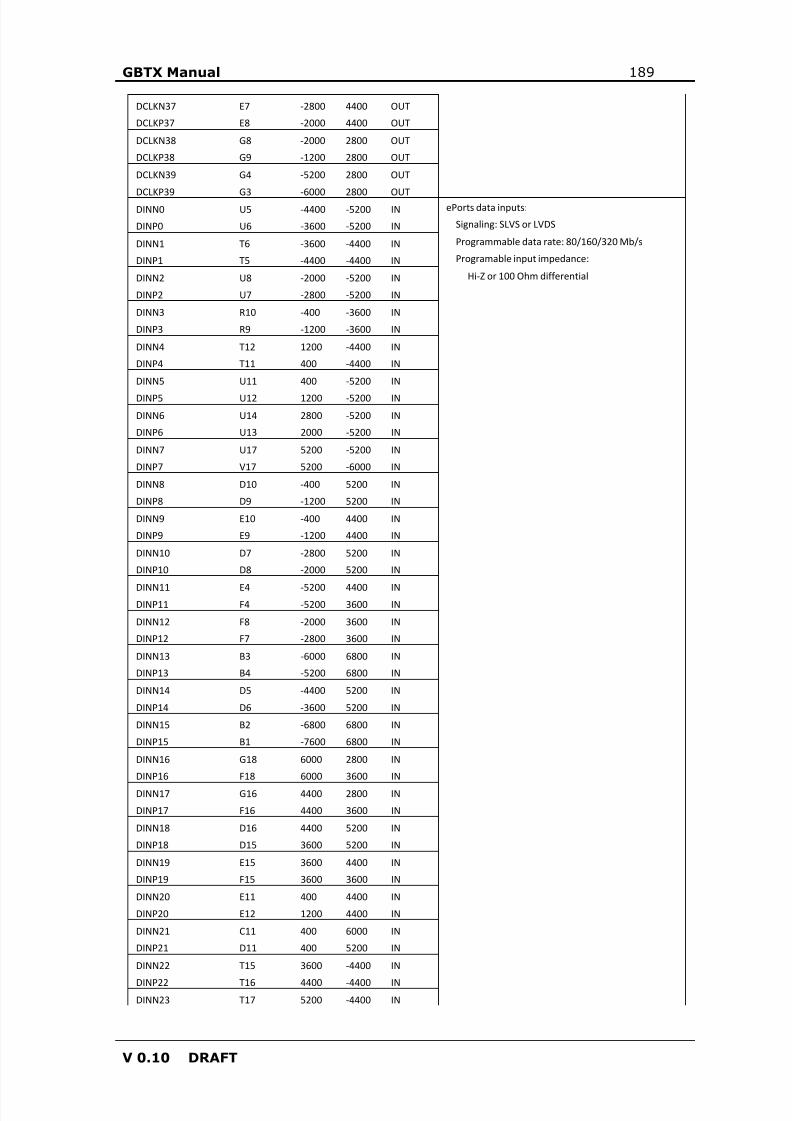
8/15/2019 gbtx Manual
http://slidepdf.com/reader/full/gbtx-manual 189/200
GBTX Manual 189
V 0.10 DRAFT
DCLKN37 E7 -2800 4400 OUT
DCLKP37 E8 -2000 4400 OUT
DCLKN38 G8 -2000 2800 OUT
DCLKP38 G9 -1200 2800 OUT
DCLKN39 G4 -5200 2800 OUT
DCLKP39 G3 -6000 2800 OUTDINN0 U5 -4400 -5200 IN ePorts data inputs:
DINP0 U6 -3600 -5200 IN Signaling: SLVS or LVDS
DINN1 T6 -3600 -4400 IN Programmable data rate: 80/160/320 Mb/s
DINP1 T5 -4400 -4400 IN Programable input impedance:
DINN2 U8 -2000 -5200 IN Hi-Z or 100 Ohm differential
DINP2 U7 -2800 -5200 IN
DINN3 R10 -400 -3600 IN
DINP3 R9 -1200 -3600 IN
DINN4 T12 1200 -4400 IN
DINP4 T11 400 -4400 IN
DINN5 U11 400 -5200 IN
DINP5 U12 1200 -5200 IN
DINN6 U14 2800 -5200 IN
DINP6 U13 2000 -5200 IN
DINN7 U17 5200 -5200 IN
DINP7 V17 5200 -6000 IN
DINN8 D10 -400 5200 IN
DINP8 D9 -1200 5200 IN
DINN9 E10 -400 4400 IN
DINP9 E9 -1200 4400 IN
DINN10 D7 -2800 5200 IN
DINP10 D8 -2000 5200 IN
DINN11 E4 -5200 4400 INDINP11 F4 -5200 3600 IN
DINN12 F8 -2000 3600 IN
DINP12 F7 -2800 3600 IN
DINN13 B3 -6000 6800 IN
DINP13 B4 -5200 6800 IN
DINN14 D5 -4400 5200 IN
DINP14 D6 -3600 5200 IN
DINN15 B2 -6800 6800 IN
DINP15 B1 -7600 6800 IN
DINN16 G18 6000 2800 IN
DINP16 F18 6000 3600 IN
DINN17 G16 4400 2800 IN
DINP17 F16 4400 3600 IN
DINN18 D16 4400 5200 IN
DINP18 D15 3600 5200 IN
DINN19 E15 3600 4400 IN
DINP19 F15 3600 3600 IN
DINN20 E11 400 4400 IN
DINP20 E12 1200 4400 IN
DINN21 C11 400 6000 IN
DINP21 D11 400 5200 IN
DINN22 T15 3600 -4400 IN
DINP22 T16 4400 -4400 INDINN23 T17 5200 -4400 IN
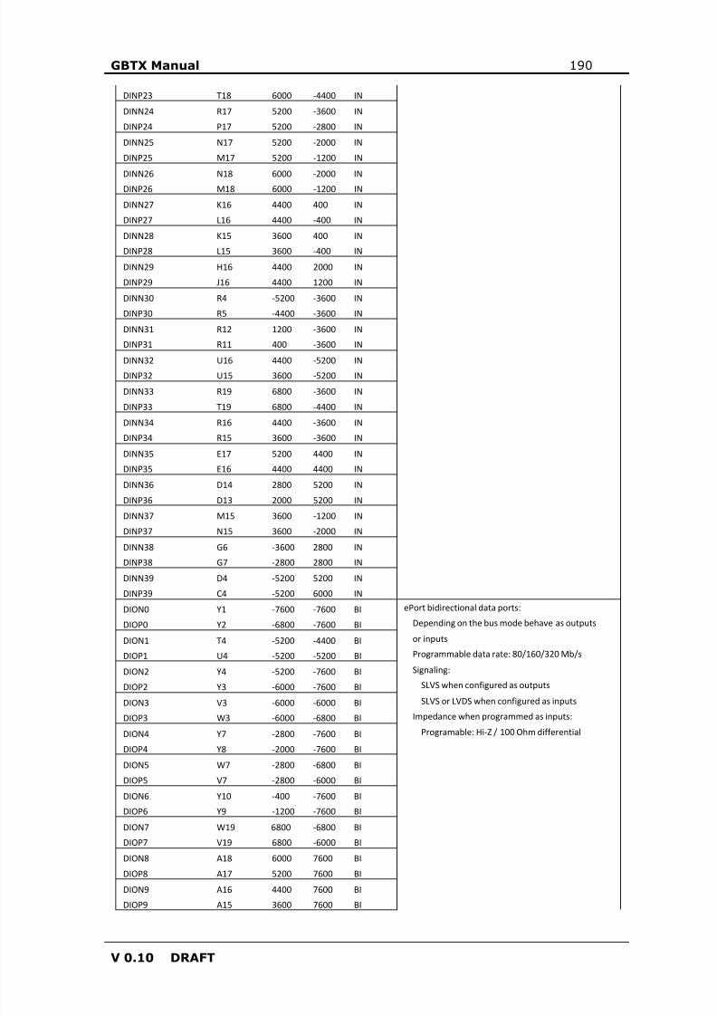
8/15/2019 gbtx Manual
http://slidepdf.com/reader/full/gbtx-manual 190/200
GBTX Manual 190
V 0.10 DRAFT
DINP23 T18 6000 -4400 IN
DINN24 R17 5200 -3600 IN
DINP24 P17 5200 -2800 IN
DINN25 N17 5200 -2000 IN
DINP25 M17 5200 -1200 IN
DINN26 N18 6000 -2000 INDINP26 M18 6000 -1200 IN
DINN27 K16 4400 400 IN
DINP27 L16 4400 -400 IN
DINN28 K15 3600 400 IN
DINP28 L15 3600 -400 IN
DINN29 H16 4400 2000 IN
DINP29 J16 4400 1200 IN
DINN30 R4 -5200 -3600 IN
DINP30 R5 -4400 -3600 IN
DINN31 R12 1200 -3600 IN
DINP31 R11 400 -3600 IN
DINN32 U16 4400 -5200 IN
DINP32 U15 3600 -5200 IN
DINN33 R19 6800 -3600 IN
DINP33 T19 6800 -4400 IN
DINN34 R16 4400 -3600 IN
DINP34 R15 3600 -3600 IN
DINN35 E17 5200 4400 IN
DINP35 E16 4400 4400 IN
DINN36 D14 2800 5200 IN
DINP36 D13 2000 5200 IN
DINN37 M15 3600 -1200 IN
DINP37 N15 3600 -2000 INDINN38 G6 -3600 2800 IN
DINP38 G7 -2800 2800 IN
DINN39 D4 -5200 5200 IN
DINP39 C4 -5200 6000 IN
DION0 Y1 -7600 -7600 BI ePort bidirectional data ports:
DIOP0 Y2 -6800 -7600 BI Depending on the bus mode behave as outputs
DION1 T4 -5200 -4400 BI or inputs
DIOP1 U4 -5200 -5200 BI Programmable data rate: 80/160/320 Mb/s
DION2 Y4 -5200 -7600 BI Signaling:
DIOP2 Y3 -6000 -7600 BI SLVS when configured as outputs
DION3 V3 -6000 -6000 BI SLVS or LVDS when configured as inputs
DIOP3 W3 -6000 -6800 BI Impedance when programmed as inputs:
DION4 Y7 -2800 -7600 BI Programable: Hi-Z / 100 Ohm differential
DIOP4 Y8 -2000 -7600 BI
DION5 W7 -2800 -6800 BI
DIOP5 V7 -2800 -6000 BI
DION6 Y10 -400 -7600 BI
DIOP6 Y9 -1200 -7600 BI
DION7 W19 6800 -6800 BI
DIOP7 V19 6800 -6000 BI
DION8 A18 6000 7600 BI
DIOP8 A17 5200 7600 BI
DION9 A16 4400 7600 BIDIOP9 A15 3600 7600 BI
8/15/2019 gbtx Manual
http://slidepdf.com/reader/full/gbtx-manual 191/200
GBTX Manual 191
V 0.10 DRAFT
DION10 A13 2000 7600 BI
DIOP10 A14 2800 7600 BI
DION11 A11 400 7600 BI
DIOP11 A12 1200 7600 BI
DION12 A10 -400 7600 BI
DIOP12 A9 -1200 7600 BI
DION13 A8 -2000 7600 BI
DIOP13 A7 -2800 7600 BI
DION14 A5 -4400 7600 BI
DIOP14 A6 -3600 7600 BI
DION15 A4 -5200 7600 BI
DIOP15 A3 -6000 7600 BI
DOUTN16 H18 6000 2000 OUT ePorts data outputs:
DOUTP16 J18 6000 1200 OUT Programmable data rates: 80/160/320 Mb/s
DOUTN17 H20 7600 2000 OUT Signaling: SLVS
DOUTP17 G20 7600 2800 OUT
DOUTN18 H19 6800 2000 OUT
DOUTP18 G19 6800 2800 OUT
DOUTN19 C19 6800 6000 OUT
DOUTP19 D19 6800 5200 OUT
DOUTN20 B20 7600 6800 OUT
DOUTP20 A20 7600 7600 OUT
DOUTN21 C18 6000 6000 OUT
DOUTP21 D18 6000 5200 OUT
DOUTN22 Y13 2000 -7600 OUT
DOUTP22 Y14 2800 -7600 OUT
DOUTN23 V14 2800 -6000 OUT
DOUTP23 V13 2000 -6000 OUT
DOUTN24 W16 4400 -6800 OUTDOUTP24 W15 3600 -6800 OUT
DOUTN25 Y20 7600 -7600 OUT
DOUTP25 Y19 6800 -7600 OUT
DOUTN26 U20 7600 -5200 OUT
DOUTP26 U19 6800 -5200 OUT
DOUTN27 N19 6800 -2000 OUT
DOUTP27 N20 7600 -2000 OUT
DOUTN28 N16 4400 -2000 OUT
DOUTP28 M16 4400 -1200 OUT
DOUTN29 K19 6800 400 OUT
DOUTP29 J19 6800 1200 OUT
DOUTN30 W2 -6800 -6800 OUT
DOUTP30 W1 -7600 -6800 OUT
DOUTN31 V8 -2000 -6000 OUT
DOUTP31 W8 -2000 -6800 OUT
DOUTN32 T13 2000 -4400 OUT
DOUTP32 T14 2800 -4400 OUT
DOUTN33 U18 6000 -5200 OUT
DOUTP33 V18 6000 -6000 OUT
DOUTN34 P20 7600 -2800 OUT
DOUTP34 P19 6800 -2800 OUT
DOUTN35 F13 2000 3600 OUT
DOUTP35 F14 2800 3600 OUTDOUTN36 B15 3600 6800 OUT
8/15/2019 gbtx Manual
http://slidepdf.com/reader/full/gbtx-manual 192/200
GBTX Manual 192
V 0.10 DRAFT
DOUTP36 B16 4400 6800 OUT
DOUTN37 C7 -2800 6000 OUT
DOUTP37 B7 -2800 6800 OUT
DOUTN38 F5 -4400 3600 OUT
DOUTP38 F6 -3600 3600 OUT
DOUTN39 A2 -6800 7600 OUTDOUTP39 A1 -7600 7600 OUT
EFUSEPOWER P14 2800 -2800 POWERE-Fuse power: 3.3V during programing, 1.5Votherwise
EFUSEPROGRAMPULSE P11 400 -2800 IN
E-Fuse write pulse
GND A19 6800 7600 GROUND Digital and digital I/O ground
GND B9 -1200 6800 GROUND
GND C13 2000 6000 GROUND
GND F10 -400 3600 GROUND
GND F11 400 3600 GROUND
GND F12 1200 3600 GROUND
GND F17 5200 3600 GROUND
GND G10 -400 2800 GROUND
GND G11 400 2800 GROUND
GND G12 1200 2800 GROUND
GND G13 2000 2800 GROUND
GND H10 -400 2000 GROUND
GND H11 400 2000 GROUND
GND H12 1200 2000 GROUND
GND J10 -400 1200 GROUND
GND J11 400 1200 GROUND
GND J20 7600 1200 GROUND
GND K11 400 400 GROUND
GND K12 1200 400 GROUND
GND L11 400 -400 GROUND
GND L12 1200 -400 GROUND
GND M11 400 -1200 GROUND
GND M12 1200 -1200 GROUND
GND P18 6000 -2800 GROUND
GND R14 2800 -3600 GROUND
GND W4 -5200 -6800 GROUND
GND W9 -1200 -6800 GROUND
GND W13 2000 -6800 GROUND
GND W17 5200 -6800 GROUND
GNDCM J1 -7600 1200 GROUND Clock manager groundGNDCM K2 -6800 400 GROUND
GNDCM L2 -6800 -400 GROUND
GNDCM M1 -7600 -1200 GROUND
GNDPS H2 -6800 2000 GROUND Phase-shifter ground
GNDPS J5 -4400 1200 GROUND
GNDPS L6 -3600 -400 GROUND
GNDPS L9 -1200 -400 GROUND
GNDPS N3 -6000 -2000 GROUND
GNDRX R1 -7600 -3600 GROUND Receiver ground
GNDRX T2 -6800 -4400 GROUND
GNDRX U2 -6800 -5200 GROUNDGNDRX V1 -7600 -6000 GROUND
8/15/2019 gbtx Manual
http://slidepdf.com/reader/full/gbtx-manual 193/200
GBTX Manual 193
V 0.10 DRAFT
GNDTX C1 -7600 6000 GROUND Transmitter ground
GNDTX C2 -6800 6000 GROUND
GNDTX D2 -6800 5200 GROUND
GNDTX E2 -6800 4400 GROUND
GNDTX F1 -7600 3600 GROUND
I2CADDRESS<0> L8 -2000 -400 IN I2C address: Bit<0> has internal pull-up to VDDIO,I2CADDRESS<1> N6 -3600 -2000 IN Bits<3:1> have internal pull-downs to GND
I2CADDRESS<2> N7 -2800 -2000 IN The resistors are 4.7 kohm.
I2CADDRESS<3> P5 -4400 -2800 IN
LDRESET J7 -2800 1200 OUT Laser driver reset
LDSCL K8 -2000 400 OUT Laser driver I2C clock
LDSDA H8 -2000 2000 BI Laser Driver I2C data
MODE<0> N5 -4400 -2000 IN Transceiver mode select signal
MODE<1> L7 -2800 -400 IN
MODE<2> L10 -400 -400 IN
MODE<3> P10 -400 -2800 IN
REFCLKN K1 -7600 400 IN Reference clock differential
REFCLKP L1 -7600 -400 IN Input impedance: 100 Ohm differential
REFCLKSELECT J9 -1200 1200 IN Selects the internal xPLL or REFCLKN/REFCLKP
RESETB M10 -400 -1200 IN Chip reset
RXDATAVALID N9 -1200 -2000 OUT Receiver data valid flag
RXINN U1 -7600 -5200 IN Receiver differential serial input. Data rate 4.8Gb/s
RXINP T1 -7600 -4400 IN Input impedance: 100 Ohm differential
RXLOCKMODE<0> J8 -2000 1200 IN Rx lock mode select signal
RXLOCKMODE<1> M9 -1200 -1200 IN
RXRDY N10 -400 -2000 OUT Receiver ready flag
SCCLKN R6 -3600 -3600 OUT Slow control ePort clock: 80 MHz
SCCLKP P6 -3600 -2800 OUT
SCINN P13 2000 -2800 IN Slow control ePort data input. Data rate 80 Mb/s
SCINP P12 1200 -2800 INProgramable input impedance: Hi-Z / 100 Ohmdifferential
SCL G5 -4400 2800 IN I2C slave clock
SCOUTN P3 -6000 -2800 OUT Slow control ePort data output. Data rate 80 Mb/s
SCOUTP P4 -5200 -2800 OUT
SDA H5 -4400 2000 BI I2C slave data line
autoReset(SLVSTESTINJECT) H15 3600 2000 IN
Enable/disable autoReset feature (GBTXv2 only) (alsoSLVS Test input)
STATEOVERRIDE H9 -1200 2000 IN Disables the automatic power-up state machine
TCK N8 -2000 -2000 IN JTAG: TCK and TDI have internal pull-ups to VDDIO.
TDI P7 -2800 -2800 IN The resistors are 4.7 kohm.
TDO P9 -1200 -2800 OUTTESTCLOCKIN1 H7 -2800 2000 IN test clock inputs
TESTCLOCKIN2 J15 3600 1200 IN
TESTCLOCKOUT H6 -3600 2000 OUT test clock output
TESTOUTPUT K10 -400 400 OUT test output
TMS P8 -2000 -2800 IN JTAG: TMS and TRESETB have internal pull-ups to
TRESETB M8 -2000 -1200 IN VDDIO. The resistors are 4.7 kohm.
TXDATAVALID N11 400 -2000 IN Transmitter data valid qualifier
TXOUTN D1 -7600 5200 OUTTransmitter differential serial output. Data rate4.8Gb/s
TXOUTP E1 -7600 4400 OUTExternal termination impedance : 100 Ohmdifferential
TXRDY L13 2000 -400 OUTTransmitter ready flag
UNUSED G17 5200 2800 n.a.
8/15/2019 gbtx Manual
http://slidepdf.com/reader/full/gbtx-manual 194/200

8/15/2019 gbtx Manual
http://slidepdf.com/reader/full/gbtx-manual 195/200
GBTX Manual 195
V 0.10 DRAFT
19. PACKAGE
Details of the GBTX ball-grid-array package can be found at the following link:https://espace.cern.ch/GBT-Project/GBTX/Manuals/Forms/AllItems.aspx
8/15/2019 gbtx Manual
http://slidepdf.com/reader/full/gbtx-manual 196/200
GBTX Manual 196
V 0.10 DRAFT
20. SC – CHANNEL PROTOCOL ENCODING/DECODING
This chapter describes the operation of the FPGA firmware used to encode anddecode the SC channel data.The encoding/decoding operations between the byte-wide frames and the 2 bitsinserted in the GBT frame are done by physical (PHY) layer blocks borrowedfrom the GBT-SCA design. These are known as PHY-TX and PHY-RX. Theiroperation is illustrated in Figure 40. The clock of these blocks is the global 40MHz clock.
Figure 44: Encoding/decoding blocks for the SC-IC bits.
The same blocks can be used for the opposite coding procedure in the FPGA atthe other end of the link.PHY-TXFor the PHY-TX, the user should assert the dValid signal when ready to starttransmitting. The dStrobe signal is generated by the PHY-TX to tell the userwhen to send a new 8-bit word of data. On average, dStrobe is asserted every
FSM Logic & registers
PHY_TX PHY_RX
SER
2 Other data
DES
2 Other data
8 data dValid dStrobe
8 data dValid dStrobe GBT-FPGA
DES SER
2 2 Other data Other data
PHY_RX
8
data dValid dStrobe
PHY_TX
8
data dValid dStrobe
GBTX
8/15/2019 gbtx Manual
http://slidepdf.com/reader/full/gbtx-manual 197/200
GBTX Manual 197
V 0.10 DRAFT
4 clock cycles (8/2), but this depends on the data content and thecorresponding bit-stuffing by the PHY-TX. All operations are synchronous to therising edge of the clock.A timing diagram is shown in Figure 41. The corresponding frame is shown inTable 32 Receiver lock mode configuration signals and the operation is thefollowing:1. The PHY-TX automatically creates the frame-delimiter 01111110 when
dValid is asserted by the user.2. The user should then wait until the PHY-TX asserts dStrobe . At the clock
edge when dStrobe is high, the user should enter the first 8-bit word ofdata (00000100).
3. At the next dStrobe and clock edge, the user should enter the next 8-bitword of data , and repeat this for each subsequent word.
4. After the last data word is entered, the PHY-TX will assert the final dStrobe which should be used by the user to de-assert the dValid .
5. The PHY-TX automatically creates the frame-delimiter 01111110 to markthe end of the frame.
Note that the number of dStrobes (9 in the example) generated by the PHY-TX will be always one more than the number of words in the frame (8 in theexample).
Figure 45: Timing diagram for the PHY-TX signals
Byte Example in diagramGBTX i2c address (7 bits) + R(1)/W(0) (1bit)
00000100 (address = 0000010,write operation)
Command (8 bits) 00000001Number of data words n[7:0] 00000001Number of data words n[15:8] 00000000 (1 byte of data)Memory address [7:0] 00001101Memory address [15:8] 00000001 (address = 269 dec)data (8 bits) 00000100Parity word (8 bits) 00001000
Table 120: Example data frame for IC configuration.
PHY-RXFor the PHY-RX, the data is validated by the dStrobe signal. A timing diagramis shown in Figure 42 for the same example as above. All operations aresynchronous to the rising edge of the clock and the operation is the following:
Figure 46 Timing diagram for the PHY-RX signals
clo da dVa dStr SC-
clo da dVa dStr SC-

8/15/2019 gbtx Manual
http://slidepdf.com/reader/full/gbtx-manual 198/200
GBTX Manual 198
V 0.10 DRAFT
1. When the PHY-RX finds the frame-delimiter, it asserts the dValid .2. Some cycles later, it asserts dStrobe for the first time. However, the data
here should be ignored.3. The second assertion of dStrobe indicates that the first data word
(00000100) is available on the bus. The data should be registered by theuser on the clock edge when dStrobe is high.
4. Each subsequent assertion of dStrobe can be used to register thecorresponding word.
5. When the PHY-RX finds the frame-delimiter at the end of frame, it de-asserts dValid .
Note that the number of dStrobes (9 in the example) generated by the PHY-RX will be always one more than the number of words in the frame (8 in theexample).
8/15/2019 gbtx Manual
http://slidepdf.com/reader/full/gbtx-manual 199/200
GBTX Manual 199
V 0.10 DRAFT
21. GBT PROJECT RELATED DOCUMENTS
The GBT project web site (http://cern.ch/proj-gbt ) makes the followingdocuments available:
GBTX Specifications (this document)
ePort SpecificationsGBTIA SpecificationsGBLD SpecificationsGBT-SCA SpecificationsGBT-FPGA project
The Versatile Link project site (https://espace.cern.ch/project-versatile-Link/default.aspx ) makes the following documents available:
Versatile Link Project description (UPDATE LISTOF DOCUMENTS FROMVERSATILE LINK)
8/15/2019 gbtx Manual
http://slidepdf.com/reader/full/gbtx-manual 200/200
GBTX Manual 200
22. REFERENCES
[1] GBTIA specifications http://cern.ch/proj-gbt [2] GBLD specifications http://cern.ch/proj-gbt [3] GBT-SCA specification http://cern.ch/proj-gbt
[4] http://www.latticesemi.com/ [5] http://www.xilinx.com/ [6] http://www.altera.com/index.jsp [7] http://www.actel.com/ [8] R. D. Schrimpf and D. M. Fleetwood, Editors, “Radiation effects and softerrors in integrated circuits and electronic devices,” World scientific publishingCo. 2004[9] H. Nussbaumer, “Computer Communication Systems: Data Circuits ErrorDetection Data Links,” Vol. 1, John Wiley & Sons, 1990[10] C.J.Marshall, P.W.Marshall, M.A.Carts, R.Reed, S.Baier, K.LaBel
“Characterization of transient error cross sections in high speed commercial
fiber optic data links”, IEEE Radiation Effects Data Workshop, 2001, pp142-145.[11] P.W.Marshall, P.T.Wiley, R.N.Prusia, G.D. Rash, H.Kim, K.A.LaBel “Protoni d d bi di i 10Gb/ Fib O i Li k” IEEE T i