Embed Size (px)
Citation preview

3.3V Uniform Sector Standard and Dual Serial Flash GD25D10C/05C
1
GD25D10C/05C
DATASHEET

3.3V Uniform Sector Standard and Dual Serial Flash GD25D10C/05C
2
CONTENTS
1. FEATURES ................................................................................................................................................................ 4
2. GENERAL DESCRIPTION ..................................................................................................................................... 5
3. MEMORY ORGANIZATION .................................................................................................................................. 7
4. DEVICE OPERATION ............................................................................................................................................. 8
5. DATA PROTECTION ............................................................................................................................................... 9
6. STATUS REGISTER ............................................................................................................................................... 10
7. COMMANDS DESCRIPTION............................................................................................................................... 11
7.1. WRITE ENABLE (WREN) (06H) ......................................................................................................................... 13
7.2. WRITE DISABLE (WRDI) (04H) ......................................................................................................................... 13
7.3. READ STATUS REGISTER (RDSR) (05H) ............................................................................................................. 13
7.4. WRITE STATUS REGISTER (WRSR) (01H) .......................................................................................................... 14
7.5. READ DATA BYTES (READ) (03H)..................................................................................................................... 15
7.6. READ DATA BYTES AT HIGHER SPEED (FAST READ) (0BH) ................................................................................ 15
7.7. DUAL OUTPUT FAST READ (3BH) ...................................................................................................................... 16
7.8. PAGE PROGRAM (PP) (02H) ................................................................................................................................ 16
7.9. SECTOR ERASE (SE) (20H) ................................................................................................................................. 17
7.10. 32KB BLOCK ERASE (BE) (52H) ....................................................................................................................... 18
7.11. 64KB BLOCK ERASE (BE) (D8H) ...................................................................................................................... 18
7.12. CHIP ERASE (CE) (60/C7H)................................................................................................................................ 19
7.13. DEEP POWER-DOWN (DP) (B9H) ....................................................................................................................... 19
7.14. RELEASE FROM DEEP POWER-DOWN / READ DEVICE ID (ABH) ........................................................................ 20
7.15. READ MANUFACTURE ID/ DEVICE ID (REMS) (90H) ........................................................................................ 21
7.16. READ IDENTIFICATION (RDID) (9FH) ................................................................................................................ 21
8. ELECTRICAL CHARACTERISTICS .................................................................................................................. 23
8.1. POWER-ON TIMING ....................................................................................................................................... 23
8.2. INITIAL DELIVERY STATE ............................................................................................................................ 23
8.3. ABSOLUTE MAXIMUM RATINGS ............................................................................................................... 23
8.4. CAPACITANCE MEASUREMENT CONDITIONS ........................................................................................ 24
8.5. DC CHARACTERISTICS................................................................................................................................. 25
8.6. AC CHARACTERISTICS................................................................................................................................. 28
9. ORDERING INFORMATION ............................................................................................................................... 32
9.1. VALID PART NUMBERS ........................................................................................................................................ 33
10. PACKAGE INFORMATION ............................................................................................................................. 35
10.1. PACKAGE SOP8 150MIL .................................................................................................................................... 35
10.2. PACKAGE SOP8 208MIL .................................................................................................................................... 36
10.3. PACKAGE TSSOP8 173MIL ............................................................................................................................... 37
10.4. PACKAGE DIP8 300MIL ..................................................................................................................................... 38

3.3V Uniform Sector Standard and Dual Serial Flash GD25D10C/05C
3
10.5. PACKAGE USON8 (1.5*1.5MM) ......................................................................................................................... 39
10.6. PACKAGE USON8 (3*2MM, 0.45MM THICKNESS) ............................................................................................... 40
11. REVISION HISTORY ........................................................................................................................................ 41

3.3V Uniform Sector Standard and Dual Serial Flash GD25D10C/05C
4
1. FEATURES
◆ 1M/512K-bit Serial Flash ◆ Fast Program/Erase Speed
-128K/64K-byte -Page Program time: 0.7ms typical
-256 bytes per programmable page -Sector Erase time: 100ms typical
-Block Erase time: 0.3/0.5s typical
◆ Standard SPI, Dual Output -Chip Erase time: 1/0.5s typical
-Standard SPI: SCLK, CS#, SI, SO, WP#
-Dual Output: SCLK, CS#, IO0, O1, WP# ◆ Flexible Architecture
-Uniform Sector of 4K-byte
◆ Clock Frequency -Uniform Block of 32/64K-byte
-100MHz for fast read with 30PF load
-Dual Output Data transfer up to 160Mbits/s ◆ Low Power Consumption
-0.1uA typical standby current
◆ Software/Hardware Write Protection -0.1uA typical power down current
-Write protect all/portion of memory via software
-Enable/Disable protection with WP# Pin ◆ Advanced Security Features
-128-bit Unique ID
◆ Minimum 100,000 Program/Erase Cycles
◆ Single Power Supply Voltage
◆ Data retention -Full voltage range: 2.7~3.6V
-20-year data retention typical
◆ Package option
-SOP8 150mil
-SOP8 208mil
-TSSOP8 173mil
-DIP8 300mil
-USON8 3*2mm
-USON8 1.5*1.5mm

3.3V Uniform Sector Standard and Dual Serial Flash GD25D10C/05C
5
2. GENERAL DESCRIPTION
The GD25D10C/05C (1M/512K-bit) Serial flash supports the standard Serial Peripheral Interface (SPI), and
supports the Dual Output: Serial Clock, Chip Select, Serial Data I/O0 (SI), O1 (SO). The Dual Output data is transferred
with speed of 160Mbits/s.
CONNECTION DIAGRAM
CS#
SO
(O1)
WP#
VSS
Top View
VCC
NC
SCLK
SI
(IO0)
8–LEAD
SOP/TSSOP/DIP
1
2
3
4 5
6
7
8 CS#
SO
(O1)
WP#
VSS
Top View
VCC
NC
SCLK
SI
(IO0)
8–LEAD USON
1
2
3
4 5
6
7
8
PIN DESCRIPTION
Pin Name I/O Description
CS# I Chip Select Input
SO (O1) O Data Output (Data Output 1)
WP# I Write Protect Input
VSS Ground
SI (IO0) I/O Data Input (Data Input Output 0)
SCLK I Serial Clock Input
NC No Connection
VCC Power Supply
Note: CS# must be driven high if chip is not selected. Please don’t leave CS# floating any time after power is on.

3.3V Uniform Sector Standard and Dual Serial Flash GD25D10C/05C
6
BLOCK DIAGRAM
SPI
Command &
Control Logic
High Voltage
Generators
Page Address
Latch/Counter
Status
Register
Write Control
Logic
Byte Address
Latch/Counter
Column Decode And
256-Byte Page Buffer
Wri
te P
rote
ct
Lo
gic
and
Ro
w D
eco
de
Flash
Memory
CS#
SCLK
SI(IO0)
SO(O1)
WP#

3.3V Uniform Sector Standard and Dual Serial Flash GD25D10C/05C
7
3. MEMORY ORGANIZATION
GD25D10C
Each device has Each block has Each sector has Each page has
128K 64/32K 4K 256 bytes
512 256/128 16 - pages
32 16/8 - - sectors
2/4 - - - blocks
GD25D05C
Each device has Each block has Each sector has Each page has
64K 64/32K 4K 256 Bytes
256 256/128 16 - pages
16 16/8 - - sectors
1/2 - - - blocks
UNIFORM BLOCK SECTOR ARCHITECTURE
GD25D10C 64K Bytes Block Sector Architecture
Block Sector Address range
1
31 01F000H 01FFFFH
…… …… ……
16 010000H 010FFFH
0
15 00F000H 00FFFFH
…… …… ……
0 000000H 000FFFH
GD25D05C 64K Bytes Block Sector Architecture
Block Sector Address range
0
15 00F000H 00FFFFH
…… …… ……
0 000000H 000FFFH

3.3V Uniform Sector Standard and Dual Serial Flash GD25D10C/05C
8
4. DEVICE OPERATION
SPI Mode
Standard SPI
The GD25D10C/05C features a serial peripheral interface on 4 signals bus: Serial Clock (SCLK), Chip Select (CS#),
Serial Data Input (SI) and Serial Data Output (SO). Both SPI bus mode 0 and 3 are supported. Input data is latched on the
rising edge of SCLK and data shifts out on the falling edge of SCLK.
Dual SPI
The GD25D10C/05C supports Dual Output operation when using the “Dual Output Fast Read” (3BH) commands.
These commands allow data to be transferred to or from the device at twice the rate of the standard SPI. When using the
Dual Output command the SI and SO pins become bidirectional I/O pins: IO0 and O1.

3.3V Uniform Sector Standard and Dual Serial Flash GD25D10C/05C
9
5. DATA PROTECTION
The GD25D10C/05C provides the following data protection methods:
◆ Write Enable (WREN) command: The WREN command is set the Write Enable Latch bit (WEL). The WEL bit will
reset to 0 in the following situations:
-Power-Up
-Write Disable (WRDI)
-Write Status Register (WRSR)
-Page Program (PP)
-Sector Erase (SE) / Block Erase (BE) / Chip Erase (CE)
◆ Software Protection Mode: The Block Protect (BP2, BP1, BP0) bits define the section of the protected memory area
which is read-only and unalterable.
◆ Hardware Protection Mode: WP# goes low to protect the BP0~BP2 bits and SRP bits.
◆ Deep Power-Down Mode: In Deep Power-Down Mode, all commands are ignored except the Release from Deep
Power-Down Mode command.
◆ Write Inhibit Voltage (VWI): Device would reset automatically when VCC is below a certain threshold VWI.
Table1(a) GD25D10C Protected area size
Status Register Content Memory Content
BP2 BP1 BP0 Blocks Addresses Density Portion
0 0 0 NONE NONE NONE NONE
0 0 1 Sector 0 to 29 000000H-01DFFFH 120KB Lower 30/32
0 1 0 Sector 0 to 27 000000H-01BFFFH 112KB Lower 28/32
0 1 1 Sector 0 to 23 000000H-017FFFH 96KB Lower 24/32
1 0 0 Sector 0 to 15 000000H-00FFFFH 64KB Lower 16/32
1 0 1 All 000000H-01FFFFH 128KB ALL
1 1 X All 000000H-01FFFFH 128KB ALL
Table1(b) GD25D05C Protected area size
Status Register Content Memory Content
BP2 BP1 BP0 Blocks Addresses Density Portion
0 0 0 NONE NONE NONE NONE
0 0 1 Sector 0 to 13 000000H-00DFFFH 56KB Lower 14/16
0 1 0 Sector 0 to 11 000000H-00BFFFH 48KB Lower 12/16
0 1 1 Sector 0 to 7 000000H-007FFFH 32KB Lower 8/16
1 X X All 000000H-00FFFFH 64KB ALL

3.3V Uniform Sector Standard and Dual Serial Flash GD25D10C/05C
10
6. STATUS REGISTER
S7 S6 S5 S4 S3 S2 S1 S0
SRP Reserved Reserved BP2 BP1 BP0 WEL WIP
The status and control bits of the Status Register are as follows:
WIP bit.
The Write In Progress (WIP) bit indicates whether the memory is busy in program/erase/write status register progress.
When WIP bit is set to 1, it means the device is busy in program/erase/write status register progress. when WIP bit is cleared
to 0, it means the device is not in program/erase/write status register progress. The default value of WIP is 0.
WEL bit.
The Write Enable Latch (WEL) bit indicates the status of the internal Write Enable Latch. When set to 1 the internal
Write Enable Latch is set, when set to 0 the internal Write Enable Latch is reset and no Write Status Register, Program or
Erase command is accepted. The default value of WEL is 0.
BP2, BP1, BP0 bits.
The Block Protect (BP2, BP1, BP0) bits are non-volatile. They define the size of the area to be software protected
against Program and Erase commands. These bits are written with the Write Status Register (WRSR) command. When the
Block Protect (BP2, BP1, BP0) bits are set to 1, the relevant memory area (as defined in Table1).becomes protected against
Page Program (PP), Sector Erase (SE) and Block Erase (BE) commands. The Block Protect (BP2, BP1, BP0) bits can be
written provided that the Hardware Protected mode has not been set. The Chip Erase (CE) command is executed, if the
Block Protect (BP2, BP1, BP0) bits are all 0. The default value of BP2:0 are 0s.
SRP bit
The Status Register Protect (SRP) bit operates in conjunction with the Write Protect (WP#) signal. The Status Register
Write Protect (SRP) bit and Write Protect (WP#) signal set the device to the Hardware Protected mode. When the Status
Register Protect (SRP) bit is set to 1, and Write Protect (WP#) is driven Low. In this mode, the non-volatile bits of the Status
Register(SRP, BP2, BP1, BP0) become read-only bits and the Write Status Register (WRSR) instruction is not execution.
The default value of SRP is 0.

3.3V Uniform Sector Standard and Dual Serial Flash GD25D10C/05C
11
7. COMMANDS DESCRIPTION
All commands, addresses and data are shifted in and out of the device by the host system, with the most significant
bit first. On the first rising edge of SCLK after CS# is driven low, the one-byte command code must be shifted into the device,
with the most significant bit first on SI, and each bit being latched on the rising edges of SCLK.
See Table2, every command sequence starts with a one-byte command code. Depending on the command, this might
be followed by address bytes, or data bytes, or dummy bytes. CS# must be driven high after the last bit of the command
sequence has been completed.
For the command of Read, Fast Read, Read Status Register or Release from Deep Power-Down, and Read Device
ID, the shifted-in command sequence is followed by a data-out sequence. All read instruction can be completed after any
bit of the data-out sequence is being shifted out, and then CS# must be driven high to return to deselected status.
For the command of Page Program, Sector Erase, Block Erase, Chip Erase, Write Status Register, Write Enable,
Write Disable or Deep Power-Down command, CS# must be driven high exactly at a byte boundary, which means the clock
pulse number should be an exact multiple of eight. Otherwise the command is rejected to executed. Especially for Page
Program command, if at any time the input end is not a completed byte, nothing will be written into the memory array, neither
would WEL bit be reset.
Table2. Commands
Command Name Byte 1 Byte 2 Byte 3 Byte 4 Byte 5 Byte 6 n-Bytes
Write Enable 06H
Write Disable 04H
Read Status Register 05H (S7-S0) (continuous)
Write Status Register 01H S7-S0
Read Data 03H A23-A16 A15-A8 A7-A0 (D7-D0) (Next byte) (continuous)
Fast Read 0BH A23-A16 A15-A8 A7-A0 dummy (D7-D0) (continuous)
Dual Output
Fast Read
3BH A23-A16 A15-A8 A7-A0 dummy (D7-D0)(1) (continuous)
Page Program 02H A23-A16 A15-A8 A7-A0 D7-D0 Next byte
Sector Erase 20H A23-A16 A15-A8 A7-A0
Block Erase(32K) 52H A23-A16 A15-A8 A7-A0
Block Erase(64K) D8H A23-A16 A15-A8 A7-A0
Chip Erase C7/60 H
Deep Power-Down B9H
Release From Deep
Power-Down, And
Read Device ID
ABH dummy dummy dummy (DID7-
DID0)
(continuous)
Release From Deep
Power-Down
ABH
Manufacturer/
Device ID
90H 00H 00H 00H (MID7-
MID0)
(DID7-
DID0)
(continuous)
Read Identification 9FH (MID7-
MID0)
(JDID15-
JDID8)
(JDID7-
JDID0)
(continuous)
Read Unique ID 4BH 00H 00H 00H dummy (UID7-
UID0)
(continuous)
NOTE:
1. Dual Output data
IO0 = (D6, D4, D2, D0)
O1 = (D7, D5, D3, D1)

3.3V Uniform Sector Standard and Dual Serial Flash GD25D10C/05C
12
TABLE OF ID DEFINATION:
GD25D10C
Operation Code M7-M0 ID15-ID8 ID7-ID0
9FH C8 40 11
90H C8 10
ABH 10
GD25D05C
Operation Code M7-M0 ID15-ID8 ID7-ID0
9FH C8 40 10
90H C8 05
ABH 05

3.3V Uniform Sector Standard and Dual Serial Flash GD25D10C/05C
13
7.1. Write Enable (WREN) (06H)
The Write Enable (WREN) command is for setting the Write Enable Latch (WEL) bit to 1. The Write Enable Latch
(WEL) bit must be set prior to every Page Program (PP), Sector Erase (SE), Block Erase (BE), Chip Erase (CE) and Write
Status Register (WRSR) command.
The Write Enable (WREN) command sequence: CS# goes low sending the Write Enable command CS# goes
high.
Figure1. Write Enable Sequence Diagram
7.2. Write Disable (WRDI) (04H)
The Write Disable command is for resetting the Write Enable Latch (WEL) bit to 0. The WEL bit is reset by following
condition: Power-up and upon completion of the Write Status Register, Page Program, Sector Erase, Block Erase and Chip
Erase commands.
The Write Disable command sequence: CS# goes lowSending the Write Disable command CS# goes high.
Figure2. Write Disable Sequence Diagram
7.3. Read Status Register (RDSR) (05H)
The Read Status Register (RDSR) command is for reading the Status Register. The Status Register may be read at
any time, even while a Program, Erase or Write Status Register cycle is in progress.
When one of these cycles is in progress, it is recommended to check the Write In Progress (WIP) bit before sending
a new command to the device. It is also possible to read the Status Register continuously. For command code “05H”, the
SO will output Status Register bits S7~S0.
Command
0 1 2 3 4 5 6 7
06H
CS#
SCLK
SI
SOHigh-Z
Command
0 1 2 3 4 5 6 7
04H
CS#
SCLK
SI
SOHigh-Z

3.3V Uniform Sector Standard and Dual Serial Flash GD25D10C/05C
14
Figure3. Read Status Register Sequence Diagram
7.4. Write Status Register (WRSR) (01H)
The Write Status Register (WRSR) instruction allows new values to be written to the Status Register. A Write Enable
(WREN) instruction must be executed previously to set the Write Enable Latch (WEL) bit, before it can be accepted.
The Write Status Register (WRSR) instruction is entered by driving Chip Select (CS#) Low, followed by the instruction
code and the data byte on Serial Data Input (DI).
The Write Status Register (WRSR) instruction has no effect on S6, S5, S1 and S0 of the Status Register. S6 and S5
are always read as 0. Chip Select (CS#) must be driven High after the eighth bit of the data byte has been latched in.
Otherwise, the Write Status Register (WRSR) instruction is not executed. As soon as Chip Select (CS#) is driven High, the
self-timed Write Status Register cycle (the duration is tW) is initiated. While the Write Status Register cycle is in progress,
reading Status Register to check the Write In Progress (WIP) bit is achievable.
The Write In Progress (WIP) bit is 1 during the self-timed Write Status Register cycle, and turn to 0 on the completion
of the Write Status Register. When the cycle is completed, the Write Enable Latch (WEL) is reset to 0.
The Write Status Register (WRSR) instruction allows the user to change the values of the Block Protect (BP2, BP1,
BP0) bits, which are utilized to define the size of the read-only area.
The Write Status Register (WRSR) instruction also allows the user to set or reset the Status Register Protect (SRP)
bit in accordance with the Write Protect (WP#) signal, by setting which the device can enter into Hardware Protected Mode
(HPM). The Write Status Register (WRSR) instruction is not executed once enter into the Hardware Protected Mode (HPM).
Figure4. Write Status Register Sequence Diagram
Command
0 1 2 3 4 5 6 7
05H
CS#
SCLK
SI
SO High-Z
8 9 10 11 12 13 14 15
7 6 5 4 3 2 1 0 7 6 5 4 3 2 1 0 7
MSB
S7~S0 out S7~S0 out
MSB
Command
0 1 2 3 4 5 6 7
01H
CS#
SCLK
SI
SO High-Z
8 9 10 11 12 13 14 15
MSB
7 6 5 4 3 2 1 0
Status Register in

3.3V Uniform Sector Standard and Dual Serial Flash GD25D10C/05C
15
7.5. Read Data Bytes (READ) (03H)
The Read Data Bytes (READ) command is followed by a 3-byte address (A23-A0), and each bit being latched-in on
the rising edge of SCLK. Then the memory content, at that address, is shifted out on SO, and each bit being shifted out, at
a Max frequency fR, on the falling edge of SCLK. The first byte addressed can be at any location. The address is
automatically incremented to the next higher address after each byte of data is shifted out. The whole memory can, therefore,
be read with a single Read Data Bytes (READ) command. Any Read Data Bytes (READ) command, while an Erase,
Program or Write cycle is in progress, is rejected without having any effects on the cycle that is in progress.
Figure5. Read Data Bytes Sequence Diagram
7.6. Read Data Bytes At Higher Speed (Fast Read) (0BH)
The Read Data Bytes at Higher Speed (Fast Read) command is for quickly reading data out. It is followed by a 3-byte
address (A23-A0) and a dummy byte, and each bit being latched-in on the rising edge of SCLK. Then the memory content,
at that address, is shifted out on SO, and each bit being shifted out, at a Max frequency fC, on the falling edge of SCLK. The
first byte addressed can be at any location. The address is automatically incremented to the next higher address after each
byte of data is shifted out.
Figure6. Read Data Bytes at Higher Speed Sequence Diagram
Command
0 1 2 3 4 5 6 7
03H
CS#
SCLK
SI
SO High-Z
8 9 10 28 29 30 31 32
MSB
3 2 1 0
34 35 36 3733
23 22 21
7 6 5 4 3 2 1 0
38 39
24-bit address
MSB
Data Out1 Data Out2
Command
0 1 2 3 4 5 6 7
0BH
CS#
SCLK
SI
SO High-Z
8 9 10 28 29 30 31
3 2 1 023 22 21
24-bit address
MSB
34 35 36 3733
6 5 4 3 2 1 0
38 39
Data Out1
32 42 43 44 4541 46 4740
7
6 5 4 3 2 1 07
6 57
Data Out2
CS#
SCLK
SI
SO
MSB
Dummy Byte

3.3V Uniform Sector Standard and Dual Serial Flash GD25D10C/05C
16
7.7. Dual Output Fast Read (3BH)
The Dual Output Fast Read command is followed by 3-byte address (A23-A0) and a dummy byte, and each bit being
latched in on the rising edge of SCLK, then the memory contents are shifted out 2-bit per clock cycle from SI and SO.
The command sequence is shown in followed Figure7. The first byte addressed can be at any location. The address is
automatically incremented to the next higher address after each byte of data is shifted out.
Figure7. Dual Output Fast Read Sequence Diagram
7.8. Page Program (PP) (02H)
The Page Program (PP) command is for programming the memory. A Write Enable (WREN) command must
previously have been executed to set the Write Enable Latch (WEL) bit before sending the Page Program command.
The Page Program (PP) command is entered by driving CS# Low, followed by the command code, three address
bytes and at least one data byte on SI.
If the 8 least significant address bits (A7-A0) are not all zero, all transmitted data that goes beyond the end of the
current page are programmed from the start address of the same page (from the address whose 8 least significant bits (A7-
A0) are all zero). CS# must be driven low for the entire duration of the sequence.
The Page Program command sequence: CS# goes low sending Page Program command 3-byte address on SI
at least 1 byte data on SI CS# goes high. The command sequence is shown in Figure8.
If more than 256 bytes are sent to the device, previously latched data are discarded and the last 256 data bytes are
guaranteed to be programmed correctly within the same page. If less than 256 data bytes are sent to device, they are
correctly programmed at the requested addresses without having any effects on the other bytes of the same page. CS#
must be driven high after the eighth bit of the last data byte has been latched in; otherwise the Page Program (PP) command
is not executed.
As soon as CS# is driven high, the self-timed Page Program cycle (whose duration is tPP) is initiated. While the Page
Program cycle is in progress, the Status Register may be read to check the value of the Write In Progress (WIP) bit. The
Write In Progress (WIP) bit is 1 during the self-timed Page Program cycle, and is 0 when it is completed. At some unspecified
time before the cycle is completed, the Write Enable Latch (WEL) bit is reset.
A Page Program (PP) command is not executed when it is applied to a page protected by the Block Protect (BP2,
BP1, BP0).
Command
0 1 2 3 4 5 6 7
3BH
CS#
SCLK
SI
SO High-Z
8 9 10 28 29 30 31
3 2 1 023 22 21
24-bit address
MSB
34 35 36 3733
5 3 1 7 5 3 1
38 39
Data Out1
32 42 43 44 4541 46 4740
7
Data Out2
CS#
SCLK
SI
SO
MSB
Dummy Clocks
4 2 0 6 4 2 06 6
7

3.3V Uniform Sector Standard and Dual Serial Flash GD25D10C/05C
17
Figure8. Page Program Sequence Diagram
7.9. Sector Erase (SE) (20H)
The Sector Erase (SE) command is for erasing the all data of the specific sector. A Write Enable (WREN) command
must previously have been executed to set the Write Enable Latch (WEL) bit. The Sector Erase (SE) command is entered
by driving CS# low, followed by the command code, and 3-address byte on SI. Any address inside the sector is a valid
address for the Sector Erase (SE) command. CS# must be driven low for the entire duration of the sequence.
The Sector Erase command sequence: CS# goes low sending Sector Erase command 3-byte address on SI
CS# goes high. The command sequence is shown in Figure9. CS# must be driven high after the eighth bit of the last address
byte has been latched in; otherwise the Sector Erase (SE) command is not executed. As soon as CS# is driven high, the
self-timed Sector Erase cycle (whose duration is tSE) is initiated. While the Sector Erase cycle is in progress, the Status
Register is accessed to check the value of the Write In Progress (WIP) bit. The Write In Progress (WIP) bit is 1 during the
self-timed Sector Erase cycle, and becomes 0 when it is completed. At some unspecified time before the cycle is completed,
the Write Enable Latch (WEL) bit is reset. A Sector Erase (SE) command applied to a sector which is protected by the Block
Protect (BP2, BP1, BP0) bit (see Table1) is not executed.
Figure9. Sector Erase Sequence Diagram
Command
0 1 2 3 4 5 6 7
02H
CS#
SCLK
SI
8 9 10 28 29 30 31
3 2 1 023 22 21
24-bit address
42 43 44 4541 46 4740 50 51 52 5349 54 5548
6 5 4 3 2 1 07
CS#
SCLK
SI
MSB
Data Byte 2
32 33 34 35
7 6 5 4 3 2 1 0
MSB
6 5 4 3 2 1 07 6 5 4 3 2 1 07
Data Byte 1
Data Byte 3 Data Byte 256
MSB MSB MSB
36 37 38 39
20
72
207
3
20
74
207
5
207
6
20
77
207
8
20
79
Command
0 1 2 3 4 5 6 7
20H
CS#
SCLK
SI
8 9 29 30 31
MSB
2 1 0
24 Bits Address
23 22

3.3V Uniform Sector Standard and Dual Serial Flash GD25D10C/05C
18
7.10. 32KB Block Erase (BE) (52H)
The 32KB Block Erase (BE) command is for erasing the all data of the chosen block. A Write Enable (WREN)
command must previously have been executed to set the Write Enable Latch (WEL) bit. The 32KB Block Erase (BE)
command is entered by driving CS# low, followed by the command code, and three address bytes on SI. Any address inside
the block is a valid address for the 32KB Block Erase (BE) command. CS# must be driven low for the entire duration of the
sequence.
The 32KB Block Erase command sequence: CS# goes low sending 32KB Block Erase command 3-byte address
on SI CS# goes high. The command sequence is shown in Figure10. CS# must be driven high after the eighth bit of the
last address byte has been latched in; otherwise the 32KB Block Erase (BE) command is not executed. As soon as CS# is
driven high, the self-timed Block Erase cycle (whose duration is tBE) is initiated. While the Block Erase cycle is in progress,
the Status Register is accessed to check the value of the Write In Progress (WIP) bit. The Write In Progress (WIP) bit is 1
during the self-timed Block Erase cycle, and becomes 0 when it is completed. At some unspecified time before the cycle is
completed, the Write Enable Latch (WEL) bit is reset. A 32KB Block Erase (BE) command applied to a block which is
protected by the Block Protect (BP2, BP1, BP0) bits (see Table1) is not executed.
Figure10. 32KB Block Erase Sequence Diagram
7.11. 64KB Block Erase (BE) (D8H)
The 64KB Block Erase (BE) command is for erasing the all data of the chosen block. A Write Enable (WREN)
command must previously have been executed to set the Write Enable Latch (WEL) bit. The 64KB Block Erase (BE)
command is entered by driving CS# low, followed by the command code, and three address bytes on SI. Any address inside
the block is a valid address for the 64KB Block Erase (BE) command. CS# must be driven low for the entire duration of the
sequence.
The 64KB Block Erase command sequence: CS# goes low sending 64KB Block Erase command 3-byte address
on SI CS# goes high. The command sequence is shown in Figure11. CS# must be driven high after the eighth bit of the
last address byte has been latched in; otherwise the 64KB Block Erase (BE) command is not executed. As soon as CS# is
driven high, the self-timed Block Erase cycle (whose duration is tBE) is initiated. While the Block Erase cycle is in progress,
the Status Register is accessed to check the value of the Write In Progress (WIP) bit. The Write In Progress (WIP) bit is 1
during the self-timed Block Erase cycle, and becomes 0 when it is completed. At some unspecified time before the cycle is
completed, the Write Enable Latch (WEL) bit is reset. A 64KB Block Erase (BE) command applied to a block which is
protected by the Block Protect (BP2, BP1, BP0) bits (see Table1) is not executed.
Command
0 1 2 3 4 5 6 7
52H
CS#
SCLK
SI
8 9 29 30 31
MSB
2 1 0
24 Bits Address
23 22

3.3V Uniform Sector Standard and Dual Serial Flash GD25D10C/05C
19
Figure11. 64KB Block Erase Sequence Diagram
7.12. Chip Erase (CE) (60/C7H)
The Chip Erase (CE) command is for erasing the all data of the chip. A Write Enable (WREN) command must
previously have been executed to set the Write Enable Latch (WEL) bit .The Chip Erase (CE) command is entered by driving
CS# Low, followed by the command code on Serial Data Input (SI). CS# must be driven Low for the entire duration of the
sequence.
The Chip Erase command sequence: CS# goes low sending Chip Erase command CS# goes high. The
command sequence is shown in Figure12. CS# must be driven high after the eighth bit of the command code has been
latched in, otherwise the Chip Erase command is not executed. As soon as CS# is driven high, the self-timed Chip Erase
cycle (whose duration is tCE) is initiated. While the Chip Erase cycle is in progress, the Status Register may be read to check
the value of the Write In Progress (WIP) bit. The Write In Progress (WIP) bit is 1 during the self-timed Chip Erase cycle, and
is 0 when it is completed. At some unspecified time before the cycle is completed, the Write Enable Latch (WEL) bit is reset.
The Chip Erase (CE) command is executed if the Block Protect (BP2, BP1, BP0) bits are all 0. The Chip Erase (CE)
command is not executed if any sector is under protection.
Figure12. Chip Erase Sequence Diagram
7.13. Deep Power-Down (DP) (B9H)
Executing the Deep Power-Down (DP) command is the only way to enter the lowest consumption mode (the Deep
Power-Down Mode). Unlike deselecting the device by driving CS# high, or entering into the Standby Mode (if there is no
internal cycle currently in progress), the Deep Power-Down Mode provides an extra software protection mechanism while
the device is not in active use. The only access to this mode is by executing the Deep Power-Down (DP) command. Since
in the Deep Power-Down mode, the device ignores all Write, Program and Erase commands. Once the device is in the
Deep Power-Down Mode, all commands are ignored except the Release from Deep Power-Down and Read Device ID (RDI)
command. The Release from Deep Power-Down and Read Device ID (RDI) command releases the device from Deep
Power-Down mode, also allows the Device ID of the device to be output on SO.
The Deep Power-Down Mode automatically stops at Power-Down, and the device is in the Standby Mode after Power-
Up.
Command
0 1 2 3 4 5 6 7
60H or C7H
CS#
SCLK
SI
Command
0 1 2 3 4 5 6 7
D8H
CS#
SCLK
SI
8 9 29 30 31
MSB
2 1 0
24 Bits Address
23 22

3.3V Uniform Sector Standard and Dual Serial Flash GD25D10C/05C
20
The Deep Power-Down command sequence: CS# goes low sending Deep Power-Down command CS# goes
high. The command sequence is shown in Figure13. CS# must be driven high after the eighth bit of the command code has
been latched in; otherwise the Deep Power-Down (DP) command is not executed. As soon as CS# is driven high, it requires
a delay of tDP before the supply current is reduced to ICC2 and the Deep Power-Down Mode is entered. Any Deep Power-
Down (DP) command, while an Erase, Program or Write cycle is in progress, is rejected without having any effects on the
cycle that is in progress.
Figure13. Deep Power-Down Sequence Diagram
7.14. Release from Deep Power-Down / Read Device ID (ABH)
The Release from Power-Down and Read Device ID command is a multi-purpose command, which can be used to
release the device from the Power-Down state or obtain the devices electronic identification (ID) number.
When used to release the device from the Power-Down state, the command is issued by driving the CS# pin low,
shifting the instruction code “ABH” and driving CS# high as shown in Figure14. Release from Power-Down will take the
time duration of tRES1 (See AC Characteristics) before the device will resume normal operation and other command are
accepted. The CS# pin must keep high during the tRES1 time duration.
When used only to obtain the Device ID while not in the Power-Down state, the command is initiated by driving the
CS# pin low and shifting the instruction code “ABH” followed by 3-dummy byte. The Device ID bits are then shifted out on
the falling edge of SCLK with most significant bit (MSB) first as shown in Figure15. The Device ID value for the
GD25D10C/05C is listed in Manufacturer and Device Identification table. The Device ID can be read continuously. The
command is completed by driving CS# high.
When used to release the device from the Power-Down state and obtain the Device ID, the command is the same
as previously described, and shown in Figure15, except that after CS# is driven high it must remain high for a time
duration of tRES2 (See AC Characteristics). After this time duration the device will resume normal operation and other
command will be accepted. If the Release from Power-Down and Read Device ID command is issued while an Erase,
Program or Write cycle is in process (when WIP equal 1) the command is ignored and will not have any effects on the
current cycle.
Figure14. Release Power-Down Sequence Diagram
Command
0 1 2 3 4 5 6 7
B9H
CS#
SCLK
SI
tDP
Stand-by mode Deep Power-down mode
Command
0 1 2 3 4 5 6 7
ABH
CS#
SCLK
SI
RES1
Stand-by modeDeep Power-down mode
t

3.3V Uniform Sector Standard and Dual Serial Flash GD25D10C/05C
21
Figure15. Release Power-Down and Read Device ID Sequence Diagram
7.15. Read Manufacture ID/ Device ID (REMS) (90H)
The Read Manufacturer/Device ID command is an alternative to the Release from Power-Down / Device ID command
that provides both the JEDEC assigned Manufacturer ID and the specific Device ID.
The command is initiated by driving the CS# pin low and shifting the command code “90H” followed by a 24-bit address
(A23-A0) of 000000H. After that, the Manufacturer ID and the Device ID are shifted out on the falling edge of SCLK with
most significant bit (MSB) first as shown in Figure16. If the 24-bit address is initially set to 000001H, the Device ID will be
read first.
Figure16. Read Manufacture ID/ Device ID Sequence Diagram
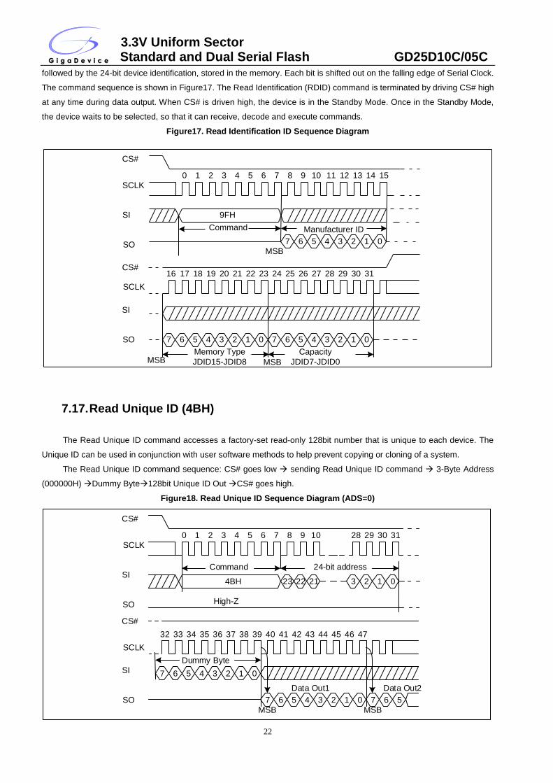
7.16. Read Identification (RDID) (9FH)
The Read Identification (RDID) command allows the 8-bit manufacturer identification to be read, followed by two bytes
of device identification. The device identification indicates the memory type in the first byte, and the memory capacity of the
device in the second byte. Any Read Identification (RDID) command while an Erase or Program cycle is in progress is not
decoded, and has no effect on the cycle that is in progress. The Read Identification (RDID) command should not be issued
while the device is in Deep Power-Down Mode.
The device is first selected by driving CS# low. Then, the 8-bit command code for the command is shifted in. This is
Command
0 1 2 3 4 5 6 7
ABH
CS#
SCLK
SI
8 9 29 30 31
MSB
2 1 0
3 Dummy Bytes
23 22
32 33 34 35 36 37 38
7 6 5 4 3 2 1 0SO
MSB
t RES2
Stand-by ModeDeep Power-down Mode
High-ZDevice ID
Command
0 1 2 3 4 5 6 7
90H
CS#
SCLK
SI
SO High-Z
8 9 10 28 29 30 31
3 2 1 023 22 21
24-bit address
MSB
34 35 36 3733
6 5 4 3 2 1 0
38 3932 42 43 44 4541 46 4740
7
Device ID
CS#
SCLK
SI
SO
MSB
Manufacturer ID
6 5 4 3 2 1 07
3.3V Uniform Sector Standard and Dual Serial Flash GD25D10C/05C
22
followed by the 24-bit device identification, stored in the memory. Each bit is shifted out on the falling edge of Serial Clock.
The command sequence is shown in Figure17. The Read Identification (RDID) command is terminated by driving CS# high
at any time during data output. When CS# is driven high, the device is in the Standby Mode. Once in the Standby Mode,
the device waits to be selected, so that it can receive, decode and execute commands.
Figure17. Read Identification ID Sequence Diagram
7.17. Read Unique ID (4BH)
The Read Unique ID command accesses a factory-set read-only 128bit number that is unique to each device. The
Unique ID can be used in conjunction with user software methods to help prevent copying or cloning of a system.
The Read Unique ID command sequence: CS# goes low sending Read Unique ID command 3-Byte Address
(000000H) Dummy Byte128bit Unique ID Out CS# goes high.
Figure18. Read Unique ID Sequence Diagram (ADS=0)
Command
0 1 2 3 4 5 6 7
4BH
CS#
SCLK
SI
SO High-Z
8 9 10 28 29 30 31
3 2 1 023 22 21
24-bit address
MSB
34 35 36 3733
6 5 4 3 2 1 0
38 39
Data Out1
32 42 43 44 4541 46 4740
7
6 5 4 3 2 1 07
6 57
Data Out2
CS#
SCLK
SI
SO
MSB
Dummy Byte
0 1 2 3 4 5 6 7
CS#
SCLK
SI
SO
8 9 10
MSB
18 19 20 2117
6 5 4 3 2 1 0
22 2316 26 27 28 2925 30 3124
7
Capacity
JDID7-JDID0
CS#
SCLK
SI
SO
MSB
Memory Type
JDID15-JDID8
6 5 4 3 2 1 07
11 12 13 14 15
9FH
6 5 4 3 2 1 07
Manufacturer ID
MSB
Command

3.3V Uniform Sector Standard and Dual Serial Flash GD25D10C/05C
23
8. ELECTRICAL CHARACTERISTICS
8.1. POWER-ON TIMING
Figure19. Power-On Timing Sequence Diagram
Table 3. Power-Up Timing and Write Inhibit Threshold
Symbol Parameter Min. Max. Unit
tVSL VCC (min.) to device operation 0.3 ms
VWI Write Inhibit Voltage 1.5 2.5 V
VPWD VCC voltage needed to below VPWD for ensuring initialization will occur 0.5 V
tPWD The minimum duration for ensuring initialization will occur 300 us
8.2. INITIAL DELIVERY STATE
The device is delivered with the memory array erased: all bits are set to 1(each byte contains FFH).The Status Register
contains 00H (all Status Register bits are 0).
8.3. ABSOLUTE MAXIMUM RATINGS
Parameter Value Unit
Ambient Operating Temperature -40 to 85
-40 to 105
-40 to 125
℃
Storage Temperature -65 to 150 ℃
Transient Input/Output Voltage (note: overshoot) -2.0 to VCC+2.0 V
Applied Input/Output Voltage -0.6 to VCC+0.4 V
VCC -0.6 to 4.2 V
VCC(max.)
VCC(min.)
tVSL
Chip Selection is not allowed
Full Device
Access
Allowed
Time
VPWD(max.)
tPWD
VCC

3.3V Uniform Sector Standard and Dual Serial Flash GD25D10C/05C
24
Figure 20. Maximum Negative/positive Overshoot
8.4. CAPACITANCE MEASUREMENT CONDITIONS
Symbol Parameter Min Tpy Max Unit Conditions
CIN Input Capacitance 6 pF VIN=0V
COUT Output Capacitance 8 pF VOUT=0V
CL Load Capacitance 30 pF
Input Rise And Fall time 5 ns
Input Pulse Voltage 0.1VCC to 0.8VCC V
Input Timing Reference Voltage 0.2VCC to 0.7VCC V
Output Timing Reference Voltage 0.5VCC V
Figure21. Diagram Input Test Waveform and Measurement Level
0.8VCC
0.1VCC
0.7VCC
0.2VCC
0.5VCCAC Measurement Level
Input timing reference level Output timing reference level
Note: Input pulse rise and fall time are <5ns
Vss
20ns
Maximum Negative Overshoot Waveform Maximum Positive Overshoot Waveform
20ns
20ns
Vss-2.0V
Vcc
20ns
20ns
20ns
Vcc + 2.0V

3.3V Uniform Sector Standard and Dual Serial Flash GD25D10C/05C
25
8.5. DC CHARACTERISTICS
(T= -40℃~85℃, VCC=2.7~3.6V)
Symbol Parameter Test Condition Min. Typ. Max. Unit.
ILI Input Leakage Current ±2 μA
ILO Output Leakage Current ±2 μA
ICC1 Standby Current CS#=VCC,
VIN=VCC or VSS
0.1 2 μA
ICC2 Deep Power-Down
Current
CS#=VCC,
VIN=VCC or VSS
0.1 2 μA
ICC3 Operating Current (Read)
CLK=0.1VCC /
0.9VCC
at 80MHz,
Q=Open(*1 I/O,*2
Output)
12 15 mA
CLK=0.1VCC /
0.9VCC
at 100MHz,
Q=Open(*1 I/O)
13 18 mA
ICC4 Operating Current (PP) CS#=VCC 20 mA
ICC5 Operating Current (WRSR) CS#=VCC 20 mA
ICC6 Operating Current (SE) CS#=VCC 20 mA
ICC7 Operating Current (BE) CS#=VCC 20 mA
ICC8 Operating Current (CE) CS#=VCC 20 mA
VIL Input Low Voltage -0.5 0.2VCC V
VIH Input High Voltage 0.7VCC VCC+0.4 V
VOL Output Low Voltage IOL = 100μA 0.4 V
VOH Output High Voltage IOH =-100μA VCC-0.2 V
Note:
1. Typical values given for TA=25°C.
2. Value guaranteed by design and/or characterization, not 100% tested in production.

3.3V Uniform Sector Standard and Dual Serial Flash GD25D10C/05C
26
(T= -40℃~105℃, VCC=2.7~3.6V)
Symbol Parameter Test Condition Min. Typ. Max. Unit.
ILI Input Leakage Current ±2 μA
ILO Output Leakage Current ±2 μA
ICC1 Standby Current CS#=VCC,
VIN=VCC or VSS
0.1 10 μA
ICC2 Deep Power-Down
Current
CS#=VCC,
VIN=VCC or VSS
0.1 10 μA
ICC3 Operating Current (Read)
CLK=0.1VCC /
0.9VCC
at 80MHz,
Q=Open(*1 I/O,*2
Output)
12 15 mA
CLK=0.1VCC /
0.9VCC
at 100MHz,
Q=Open(*1 I/O)
13 18 mA
ICC4 Operating Current (PP) CS#=VCC 20 mA
ICC5 Operating Current (WRSR) CS#=VCC 20 mA
ICC6 Operating Current (SE) CS#=VCC 20 mA
ICC7 Operating Current (BE) CS#=VCC 20 mA
ICC8 Operating Current (CE) CS#=VCC 20 mA
VIL Input Low Voltage -0.5 0.2VCC V
VIH Input High Voltage 0.7VCC VCC+0.4 V
VOL Output Low Voltage IOL = 100μA 0.4 V
VOH Output High Voltage IOH =-100μA VCC-0.2 V
Note:
1. Typical values given for TA=25°C.
2. Value guaranteed by design and/or characterization, not 100% tested in production.

3.3V Uniform Sector Standard and Dual Serial Flash GD25D10C/05C
27
(T= -40℃~125℃, VCC=2.7~3.6V)
Symbol Parameter Test Condition Min. Typ. Max. Unit.
ILI Input Leakage Current ±2 μA
ILO Output Leakage Current ±2 μA
ICC1 Standby Current CS#=VCC,
VIN=VCC or VSS
0.1 15 μA
ICC2 Deep Power-Down
Current
CS#=VCC,
VIN=VCC or VSS
0.1 15 μA
ICC3 Operating Current (Read)
CLK=0.1VCC /
0.9VCC
at 80MHz,
Q=Open(*1 I/O,*2
Output)
12 15 mA
CLK=0.1VCC /
0.9VCC
at 100MHz,
Q=Open(*1 I/O)
13 18 mA
ICC4 Operating Current (PP) CS#=VCC 20 mA
ICC5 Operating Current (WRSR) CS#=VCC 20 mA
ICC6 Operating Current (SE) CS#=VCC 20 mA
ICC7 Operating Current (BE) CS#=VCC 20 mA
ICC8 Operating Current (CE) CS#=VCC 20 mA
VIL Input Low Voltage -0.5 0.2VCC V
VIH Input High Voltage 0.7VCC VCC+0.4 V
VOL Output Low Voltage IOL = 100μA 0.4 V
VOH Output High Voltage IOH =-100μA VCC-0.2 V
Note:
1. Typical values given for TA=25°C.
2. Value guaranteed by design and/or characterization, not 100% tested in production.
3.3V Uniform Sector Standard and Dual Serial Flash GD25D10C/05C
28
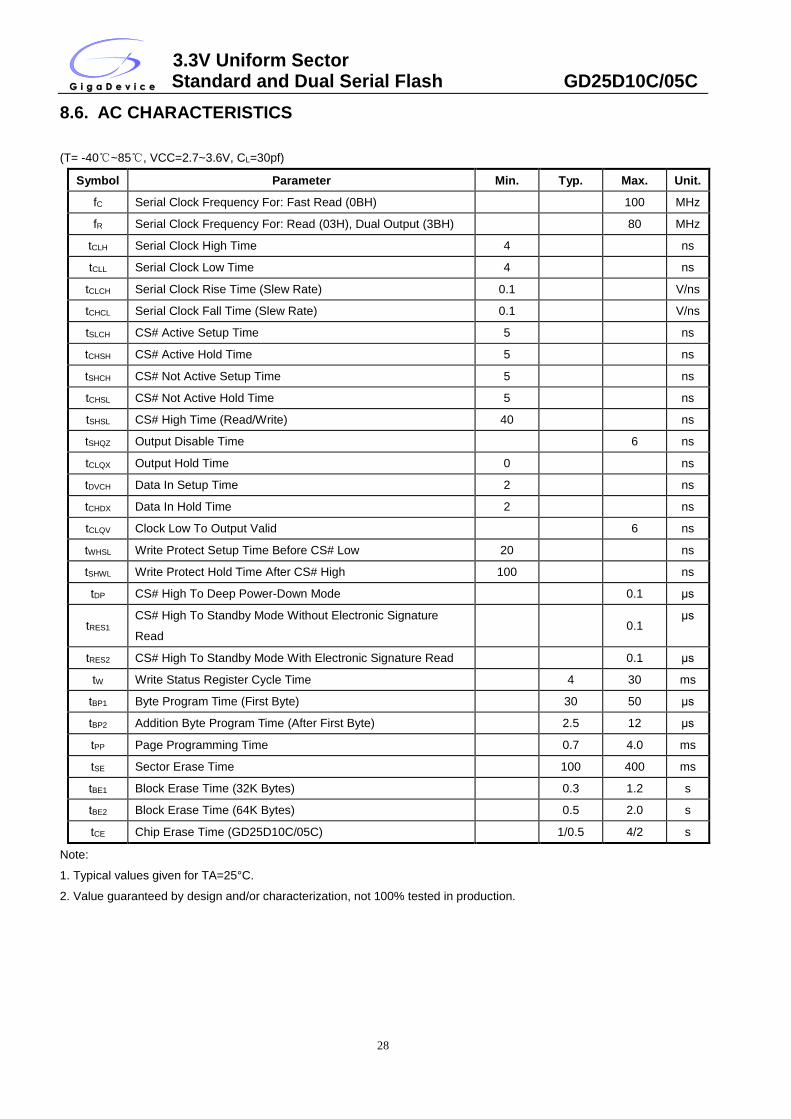
8.6. AC CHARACTERISTICS
(T= -40℃~85℃, VCC=2.7~3.6V, CL=30pf)
Symbol Parameter Min. Typ. Max. Unit.
fC Serial Clock Frequency For: Fast Read (0BH) 100 MHz
fR Serial Clock Frequency For: Read (03H), Dual Output (3BH) 80 MHz
tCLH Serial Clock High Time 4 ns
tCLL Serial Clock Low Time 4 ns
tCLCH Serial Clock Rise Time (Slew Rate) 0.1 V/ns
tCHCL Serial Clock Fall Time (Slew Rate) 0.1 V/ns
tSLCH CS# Active Setup Time 5 ns
tCHSH CS# Active Hold Time 5 ns
tSHCH CS# Not Active Setup Time 5 ns
tCHSL CS# Not Active Hold Time 5 ns
tSHSL CS# High Time (Read/Write) 40 ns
tSHQZ Output Disable Time 6 ns
tCLQX Output Hold Time 0 ns
tDVCH Data In Setup Time 2 ns
tCHDX Data In Hold Time 2 ns
tCLQV Clock Low To Output Valid 6 ns
tWHSL Write Protect Setup Time Before CS# Low 20 ns
tSHWL Write Protect Hold Time After CS# High 100 ns
tDP CS# High To Deep Power-Down Mode 0.1 μs
tRES1 CS# High To Standby Mode Without Electronic Signature
Read 0.1
μs
tRES2 CS# High To Standby Mode With Electronic Signature Read 0.1 μs
tW Write Status Register Cycle Time 4 30 ms
tBP1 Byte Program Time (First Byte) 30 50 μs
tBP2 Addition Byte Program Time (After First Byte) 2.5 12 μs
tPP Page Programming Time 0.7 4.0 ms
tSE Sector Erase Time 100 400 ms
tBE1 Block Erase Time (32K Bytes) 0.3 1.2 s
tBE2 Block Erase Time (64K Bytes) 0.5 2.0 s
tCE Chip Erase Time (GD25D10C/05C) 1/0.5 4/2 s
Note:
1. Typical values given for TA=25°C.
2. Value guaranteed by design and/or characterization, not 100% tested in production.

3.3V Uniform Sector Standard and Dual Serial Flash GD25D10C/05C
29
(T= -40℃~105℃, VCC=2.7~3.6V, CL=30pf)
Symbol Parameter Min. Typ. Max. Unit.
fC Serial Clock Frequency For: Fast Read (0BH) 100 MHz
fR Serial Clock Frequency For: Read (03H), Dual Output (3BH) 80 MHz
tCLH Serial Clock High Time 4 ns
tCLL Serial Clock Low Time 4 ns
tCLCH Serial Clock Rise Time (Slew Rate) 0.1 V/ns
tCHCL Serial Clock Fall Time (Slew Rate) 0.1 V/ns
tSLCH CS# Active Setup Time 5 ns
tCHSH CS# Active Hold Time 5 ns
tSHCH CS# Not Active Setup Time 5 ns
tCHSL CS# Not Active Hold Time 5 ns
tSHSL CS# High Time (Read/Write) 40 ns
tSHQZ Output Disable Time 6 ns
tCLQX Output Hold Time 0 ns
tDVCH Data In Setup Time 2 ns
tCHDX Data In Hold Time 2 ns
tCLQV Clock Low To Output Valid 6 ns
tWHSL Write Protect Setup Time Before CS# Low 20 ns
tSHWL Write Protect Hold Time After CS# High 100 ns
tDP CS# High To Deep Power-Down Mode 0.1 μs
tRES1 CS# High To Standby Mode Without Electronic Signature
Read 0.1
μs
tRES2 CS# High To Standby Mode With Electronic Signature Read 0.1 μs
tW Write Status Register Cycle Time 4 30 ms
tBP1 Byte Program Time (First Byte) 30 60 μs
tBP2 Addition Byte Program Time (After First Byte) 2.5 15 μs
tPP Page Programming Time 0.7 4.0 ms
tSE Sector Erase Time 100 400 ms
tBE1 Block Erase Time (32K Bytes) 0.3 1.2 s
tBE2 Block Erase Time (64K Bytes) 0.5 2.0 s
tCE Chip Erase Time (GD25D10C/05C) 1/0.5 4/2 s
Note:
1. Typical values given for TA=25°C.
2. Value guaranteed by design and/or characterization, not 100% tested in production.

3.3V Uniform Sector Standard and Dual Serial Flash GD25D10C/05C
30
(T= -40℃~125℃, VCC=2.7~3.6V, CL=30pf)
Symbol Parameter Min. Typ. Max. Unit.
fC Serial Clock Frequency For: Fast Read (0BH) 100 MHz
fR Serial Clock Frequency For: Read (03H), Dual Output (3BH) 80 MHz
tCLH Serial Clock High Time 4 ns
tCLL Serial Clock Low Time 4 ns
tCLCH Serial Clock Rise Time (Slew Rate) 0.1 V/ns
tCHCL Serial Clock Fall Time (Slew Rate) 0.1 V/ns
tSLCH CS# Active Setup Time 5 ns
tCHSH CS# Active Hold Time 5 ns
tSHCH CS# Not Active Setup Time 5 ns
tCHSL CS# Not Active Hold Time 5 ns
tSHSL CS# High Time (Read/Write) 40 ns
tSHQZ Output Disable Time 6 ns
tCLQX Output Hold Time 0 ns
tDVCH Data In Setup Time 2 ns
tCHDX Data In Hold Time 2 ns
tCLQV Clock Low To Output Valid 6 ns
tWHSL Write Protect Setup Time Before CS# Low 20 ns
tSHWL Write Protect Hold Time After CS# High 100 ns
tDP CS# High To Deep Power-Down Mode 0.1 μs
tRES1 CS# High To Standby Mode Without Electronic Signature
Read 0.1
μs
tRES2 CS# High To Standby Mode With Electronic Signature Read 0.1 μs
tW Write Status Register Cycle Time 4 30 ms
tBP1 Byte Program Time (First Byte) 30 80 μs
tBP2 Addition Byte Program Time (After First Byte) 2.5 20 μs
tPP Page Programming Time 0.7 4.0 ms
tSE Sector Erase Time 100 400 ms
tBE1 Block Erase Time (32K Bytes) 0.3 1.2 s
tBE2 Block Erase Time (64K Bytes) 0.5 2.0 s
tCE Chip Erase Time (GD25D10C/05C) 1/0.5 4/2 s
Note:
1. Typical values given for TA=25°C.
2. Value guaranteed by design and/or characterization, not 100% tested in production.

3.3V Uniform Sector Standard and Dual Serial Flash GD25D10C/05C
31
Figure22. Serial Input Timing
Figure23. Output Timing
SCLK
CS#
SI MSB
SO High-Z
LSB
tCHSL tSLCH
tDVCHtCHDX
tSHCHtCHSH
tCHCLtCLCH
tSHSL
CS#
SCLK
SO
SI
Least significant address bit (LIB) in
tCLQV
tCLQX tCLQX
tCLQV
tCLH
tCLL
tSHQZ
LSB

3.3V Uniform Sector Standard and Dual Serial Flash GD25D10C/05C
32
9. ORDERING INFORMATION
*Please contact GigaDevice sales for automotive products.
Packing
T or no mark: Tube
Y: Tray
R: Tape and Reel
Green Code
G: Pb Free + Halogen Free Green Package
Temperature Range
I: Industrial (-40℃ to +85℃)
J: Industrial (-40℃ to +105℃)
E: Industrial (-40℃ to +125℃)
F: Industrial+ (-40℃ to +85℃)
3: Automotive (-40℃ to +85℃)*
2: Automotive (-40℃ to +105℃)*
A: Automotive (-40℃ to +125℃)*
Package Type
T: SOP8 150mil
S: SOP8 208mil
O: TSSOP8 173mil
P: DIP8 300mil
K: USON8 (1.5x1.5mm)
E: USON8 (3x2mm, 0.45mm thickness)
Generation
C: C Version
Density
10: 1M bit
05: 512K bit
Series
D: 3V, 4KB Uniform Sector
Product Family
25: SPI Interface Flash
X X XGD XX XX XX X X

3.3V Uniform Sector Standard and Dual Serial Flash GD25D10C/05C
33
9.1. Valid Part Numbers
Please contact GigaDevice regional sales for the latest product selection and available form factors.
Temperature Range I: Industrial (-40℃ to +85℃)
Product Number Density Package Type
GD25D10CTIG 1Mbit SOP8 150mil
GD25D05CTIG 512Kbit
GD25D10CSIG 1Mbit SOP8 208mil
GD25D05CSIG 512Kbit
GD25D10COIG 1Mbit TSSOP8 173mil
GD25D05COIG 512Kbit
GD25D10CPIG 1Mbit DIP8 300mil
GD25D05CPIG 512Kbit
GD25D10CKIG 1Mbit USON8 (1.5x1.5mm)
GD25D05CKIG 512Kbit
GD25D10CEIG 1Mbit USON8 (3x2mm, 0.45mm thickness)
GD25D05CEIG 512Kbit
Temperature Range J: Industrial (-40℃ to +105℃)
Product Number Density Package Type
GD25D10CTJG 1Mbit SOP8 150mil
GD25D05CTJG 512Kbit
GD25D10CSJG 1Mbit SOP8 208mil
GD25D05CSJG 512Kbit
GD25D10COJG 1Mbit TSSOP8 173mil
GD25D05COJG 512Kbit
GD25D10CPJG 1Mbit DIP8 300mil
GD25D05CPJG 512Kbit
GD25D10CKJG 1Mbit USON8 (1.5x1.5mm)
GD25D05CKJG 512Kbit
GD25D10CEJG 1Mbit USON8 (3x2mm, 0.45mm thickness)
GD25D05CEJG 512Kbit

3.3V Uniform Sector Standard and Dual Serial Flash GD25D10C/05C
34
Temperature Range E: Industrial (-40℃ to +125℃)
Product Number Density Package Type
GD25D10CTEG 1Mbit SOP8 150mil
GD25D05CTEG 512Kbit
GD25D10CSEG 1Mbit SOP8 208mil
GD25D05CSEG 512Kbit
GD25D10COEG 1Mbit TSSOP8 173mil
GD25D05COEG 512Kbit
GD25D10CPEG 1Mbit DIP8 300mil
GD25D05CPEG 512Kbit
GD25D10CKEG 1Mbit USON8 (1.5x1.5mm)
GD25D05CKEG 512Kbit
GD25D10CEEG 1Mbit USON8 (3x2mm, 0.45mm thickness)
GD25D05CEEG 512Kbit
Temperature Range F: Industrial+ (-40℃ to +85℃)
Product Number Density Package Type
GD25D10CTFG 1Mbit SOP8 150mil
GD25D05CTFG 512Kbit
GD25D10CSFG 1Mbit SOP8 208mil
GD25D05CSFG 512Kbit
GD25D10COFG 1Mbit TSSOP8 173mil
GD25D05COFG 512Kbit
GD25D10CPFG 1Mbit DIP8 300mil
GD25D05CPFG 512Kbit
GD25D10CKFG 1Mbit USON8 (1.5x1.5mm)
GD25D05CKFG 512Kbit
GD25D10CEFG 1Mbit USON8 (3x2mm, 0.45mm thickness)
GD25D05CEFG 512Kbit

3.3V Uniform Sector Standard and Dual Serial Flash GD25D10C/05C
35
10. PACKAGE INFORMATION
10.1. Package SOP8 150MIL
D
E E1
A A2
A1b e
“A”
L1L
θ
b
c
Base Metal
Detail “A”
h
1 4
8 5
Dimensions
Symbol A A1 A2 b c D E E1 e L L1 h θ
Unit
mm
Min - 0.10 1.25 0.31 0.10 4.80 5.80 3.80
1.27
0.40
1.04
0.25 0°
Nom - 0.15 1.45 0.41 0.20 4.90 6.00 3.90 - - -
Max 1.75 0.25 1.55 0.51 0.25 5.00 6.20 4.00 0.90 0.50 8°
Note:
1. Both the package length and width include the mold flash.
2. Seating plane: Max. 0.1mm.

3.3V Uniform Sector Standard and Dual Serial Flash GD25D10C/05C
36
10.2. Package SOP8 208MIL
D
E E1
A A2
A1b e
“A”
L1L
θ
b
c
Base Metal
Detail “A”
1 4
8 5
Dimensions
Symbol A A1 A2 b c D E E1 e L L1 θ
Unit
mm
Min - 0.05 1.70 0.31 0.15 5.13 7.70 5.18
1.27
0.50
1.31
0°
Nom - 0.15 1.80 0.41 0.20 5.23 7.90 5.28 - -
Max 2.16 0.25 1.90 0.51 0.25 5.33 8.10 5.38 0.85 8°
Note:
1. Both the package length and width do not include the mold flash.
2. Seating plane: Max. 0.1mm.

3.3V Uniform Sector Standard and Dual Serial Flash GD25D10C/05C
37
10.3. Package TSSOP8 173MIL
D
E E1
A
A1
A2
b e
“A”
L1L
θ
b
c
Base Metal
Detail “A”
1 4
8 5
Dimensions
Symbol A A1 A2 b c D E E1 e L L1 θ
Unit
mm
Min - 0.05 0.80 0.19 0.09 2.90 6.20 4.30
0.65
0.45
1.00
0°
Nom - 0.10 1.00 0.25 0.15 3.00 6.40 4.40 - -
Max 1.20 0.15 1.05 0.30 0.20 3.10 6.60 4.50 0.75 8°
Notes:
1. Both package length and width do not include mold flash.
2. Seating plane: Max. 0.1mm.

3.3V Uniform Sector Standard and Dual Serial Flash GD25D10C/05C
38
10.4. Package DIP8 300MIL
E
E1
AA2
A1
b1 e
θ
D
L
b
eA
14
85
c
Dimensions
Symbol A A1 A2 b b1 C D E E1 e L eA θ
Unit
mm
Min - 0.38 3.00 1.14 0.36 0.20 9.02 7.62 6.10
2.54
2.92 8.45 0°
Nom - - 3.30 1.52 0.46 0.25 9.27 7.87 6.35 3.30 8.90 -
Max 3.88 - 3.50 1.78 0.56 0.35 9.59 8.26 6.60 3.81 9.35 11°
Note: Both the package length and width do not include the mold flash.

3.3V Uniform Sector Standard and Dual Serial Flash GD25D10C/05C
39
10.5. Package USON8 (1.5*1.5mm)
Dimensions
Symbol A A1 A2 A3 b D E D1 E1 D2 E2 e L L1 K K1 K2
Unit
mm
Min 0.40 0.00 0.33
REF
0.127
REF
0.13 1.40 1.40 0.20
REF
0.05
REF
0.60 1.20 0.40
REF
0.125 0.06
REF
0.20
REF
0.10
REF
0.15
REF Nom 0.45 0.02 0.18 1.50 1.50 0.70 1.30 0.20
Max 0.50 0.05 0.25 1.60 1.60 0.80 1.40 0.25
Note:
1. Both the package length and width do not include the mold flash.
2. The exposed metal pad area on the bottom of the package is floating.
3. Coplanarity ≤0.08mm. Package edge tolerance≤0.10mm.
4. The lead shape may be of little difference according to different package factories. These lead shapes
are compatible with each other.
D
E
Top View
D1
E2
L1
e
Bottom View
A1
Side View
1
4
8
5
K1
PIN 1#
A3
A
K
E1
L
b
K2
D2
A2

3.3V Uniform Sector Standard and Dual Serial Flash GD25D10C/05C
40
10.6. Package USON8 (3*2mm, 0.45mm thickness)
D
E
Top View
L
E1
D1L1
b
Bottom View
Note(4)
e
A1
Side View
c
ANote(4)
1
4
8
5
PIN 1#
or
or
Dimensions
Symbol A A1 c b D D1 E E1 e L L1
Unit
mm
Min 0.40 0.00 0.10 0.20 2.90 0.15 1.90 1.55
0.50
0.30
0.10 Nom 0.45 0.02 0.15 0.25 3.00 0.20 2.00 1.60 0.35
Max 0.50 0.05 0.20 0.30 3.10 0.25 2.10 1.65 0.40
Note:
1. Both the package length and width do not include the mold flash.
2. The exposed metal pad area on the bottom of the package is floating.
3. Coplanarity ≤0.08mm. Package edge tolerance≤0.10mm.
4. The lead shape may be of little difference according to different package factories. These lead shapes
are compatible with each other.

3.3V Uniform Sector Standard and Dual Serial Flash GD25D10C/05C
41
11. REVISION HISTORY
Version No Description Page Date
1.0 Initial Released All 2017-12-12
1.1 Modify tVSL from 5ms to 0.5ms
Add “F”, “3”, “2”, and “A” to the 7th code of the Ordering Information
P23
P28 2018-4-16
1.2 Modify tBP1 from 25~50us to 30~50us
Modify tBP2 from 2.5~5us to 2.5~12us
P26
P26 2018-4-23
1.3 Modify tVSL min value from 0.5ms to 0.3ms
Add package of USON8 1.5*1.5mm
P23
P28, 29, 34 2018-5-30
1.4
Add 4BH command
Add DC/AC characteristics @-40℃~105℃
Add DC/AC characteristics @-40℃~125℃
Modify Ordering Information
Modify Package USON8 1.5*1.5mm Dimensions
P12
P26/29
P27/30
P32
P39
2018-7-17

3.3V Uniform Sector Standard and Dual Serial Flash GD25D10C/05C
42
Important Notice
This document is the property of GigaDevice Semiconductor (Beijing) Inc. and its subsidiaries (the "Company"). This
document, including any product of the Company described in this document (the “Product”), is owned by the Company
under the intellectual property laws and treaties of the People’s Republic of China and other jurisdictions worldwide. The
Company reserves all rights under such laws and treaties and does not grant any license under its patents, copyrights,
trademarks, or other intellectual property rights. The names and brands of third party referred thereto (if any) are the property
of their respective owner and referred to for identification purposes only.
The Company makes no warranty of any kind, express or implied, with regard to this document or any Product,
including, but not limited to, the implied warranties of merchantability and fitness for a particular purpose. The Company
does not assume any liability arising out of the application or use of any Product described in this document. Any information
provided in this document is provided only for reference purposes. It is the responsibility of the user of this document to
properly design, program, and test the functionality and safety of any application made of this information and any resulting
product. Except for customized products which has been expressly identified in the applicable agreement, the Products are
designed, developed, and/or manufactured for ordinary business, industrial, personal, and/or household applications only.
The Products are not designed, intended, or authorized for use as components in systems designed or intended for the
operation of weapons, weapons systems, nuclear installations, atomic energy control instruments, combustion control
instruments, airplane or spaceship instruments, traffic signal instruments, life-support devices or systems, other medical
devices or systems (including resuscitation equipment and surgical implants), pollution control or hazardous substances
management, or other uses where the failure of the device or Product could cause personal injury, death, property or
environmental damage ("Unintended Uses"). Customers shall take any and all actions to ensure using and selling the
Products in accordance with the applicable laws and regulations. The Company is not liable, in whole or in part, and
customers shall and hereby do release the Company as well as it’s suppliers and/or distributors from any claim, damage,
or other liability arising from or related to all Unintended Uses of the Products. Customers shall indemnify and hold the
Company as well as it’s suppliers and/or distributors harmless from and against all claims, costs, damages, and other
liabilities, including claims for personal injury or death, arising from or related to any Unintended Uses of the Products.
Information in this document is provided solely in connection with the Products. The Company reserves the
right to make changes, corrections, modifications or improvements to this document and the Products and
services described herein at any time, without notice.