Embed Size (px)
Citation preview
Low Power Stereo Audio DAC
With Headphone Amplifier
Version 1.0 3/29/2011 1
ES8155
GENERAL DESCRIPTION FEATURES ES8155 is a high performance, low power and low cost audio DAC. It consists of 2-ch DAC, headphone amplifier, digital sound effects, and analog mixing and gain functions. The device uses advanced multi-bit delta-sigma modulation technique to convert data between digital and analog. The multi-bit delta-sigma modulators make the device with low sensitivity to clock jitter and low out of band noise.
DAC • 24-bit, 8 kHz to 96 kHz sampling frequency • 96 dB dynamic range, 96 dB signal to noise ratio,
-83 dB THD+N • 40 mW headphone amplifier, pop noise free,
capless option • Stereo enhancement • 3-band fully parametric graphic equalizer • Various analog output mixing and gains Low Power • 1.8V to 3.3V operation • 7 mW playback System • I2C or SPI uC interface • 256Fs, 384Fs, USB 12 MHz or 24 MHz • Fractional PLL for wide range of system clocks • Master or slave serial port • I2S, Left Justified, Right Justified, DSP Mode
APPLICATIONS ORDERING INFORMATION • Cell phone • GPS • MP3, MP4, PMP • Digital camera, camcorder • Bluetooth • Portable audio devices
ES8155 -40°C ~ +85°C QFN-28
Everest Semiconductor ES8155
Version 1.0 3/29/2011 2
1 BLOCK DIAGRAM ..................................................................................... 4 2 28-PIN QFN AND PIN DESCRIPTIONS .................................................... 5 3 TYPICAL APPLICATION CIRCUIT ............................................................ 6 4 CLOCK MODES AND SAMPLING FREQUENCIES.................................. 6 5 MICRO-CONTROLLER CONFIGURATION INTERFACE ......................... 9
5.1 SPI ...................................................................................................... 9 5.2 2-wire ................................................................................................ 10
6 CONFIGURATION REGISTER DEFINITION .......................................... 11 6.1 Output Setting ................................................................................... 15
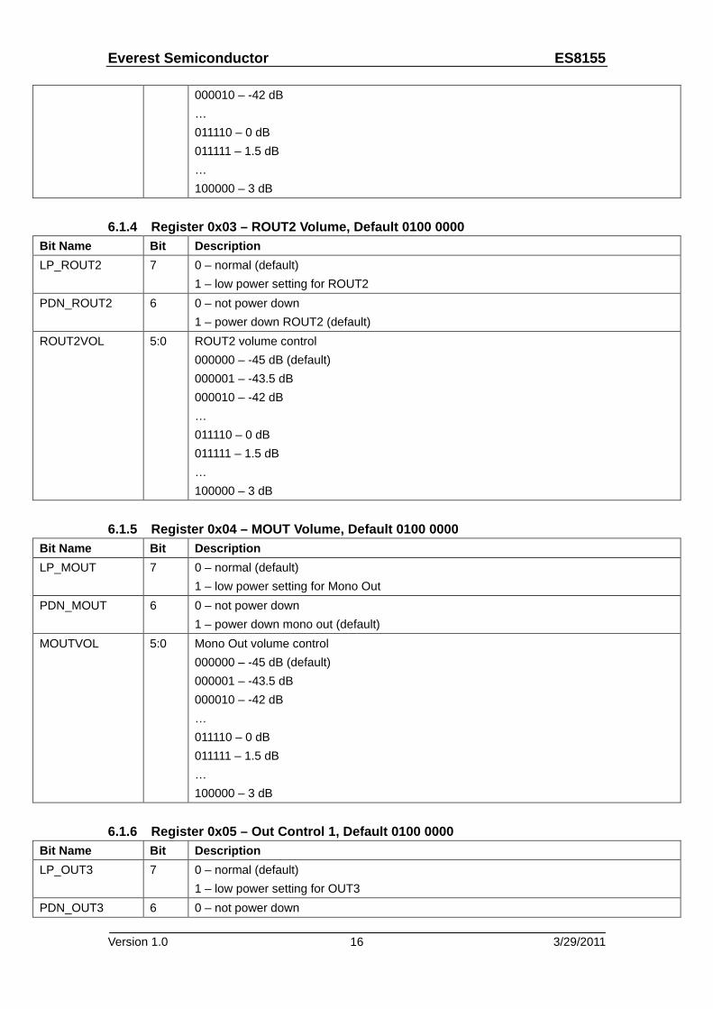
6.1.1 Register 0x00 – LOUT1 Volume, Default 0100 0000 .................. 15 6.1.2 Register 0x01 – ROUT1 Volume, Default 0100 0000 .................. 15 6.1.3 Register 0x02 – LOUT2 Volume, Default 0100 0000 .................. 15 6.1.4 Register 0x03 – ROUT2 Volume, Default 0100 0000 .................. 16 6.1.5 Register 0x04 – MOUT Volume, Default 0100 0000 ................... 16 6.1.6 Register 0x05 – Out Control 1, Default 0100 0000 ...................... 16 6.1.7 Register 0x06 – Out Control 2, Default 0000 0000 ...................... 17
6.2 Mixer Setting ..................................................................................... 17 6.2.1 Register 0x07 – Left Mixer, Default 1111 1111 ............................. 17 6.2.2 Register 0x08 – Right Mixer, Default 1111 1111 ........................... 18 6.2.3 Register 0x09 – Mono Mixer, Default 1111 1111 .......................... 18 6.2.4 Register 0x0A – DAC to Mixer, Default 1011 1111 ....................... 19 6.2.5 Register 0x0B – Mixer LP Mode, Default 0000 0000 .................. 19
6.3 DAC Setting ....................................................................................... 19 6.3.1 Register 0x0C – Left DAC Volume, Default 1100 0000 ............... 19 6.3.2 Register 0x0D – Right DAC Volume, Default 1100 0000 ............. 20 6.3.3 Register 0x0E – DAC Control 1, Default 0101 0101 ................... 20 6.3.4 Register 0x0F – DAC Control 2, Default 1100 0100 .................... 20 6.3.5 Register 0x10 DAC Control 3, Default 0000 1000 ....................... 21 6.3.6 Register 0x11– DAC Control 4, Default 0000 0000 ..................... 21 6.3.7 Register 0x12– SHELVING1_A[29:24], Default 0001 1111.......... 21 6.3.8 Register 0x13– SHELVING1_A[23:16], Default 1111 0111 .......... 21 6.3.9 Register 0x14– SHELVING1_A[15:8], Default 1111 1101 ............ 21 6.3.10 Register 0x15– SHELVING1_A[7:0], Default 1111 1111 .............. 21 6.3.11 Register 0x16– SHELVING1_B[29:24], Default 0001 1111.......... 21 6.3.12 Register 0x17– SHELVING1_B[23:16], Default 1111 0111 .......... 22 6.3.13 Register 0x18– SHELVING1_B[15:8], Default 1111 1101 ............ 22 6.3.14 Register 0x19– SHELVING1_B[7:0], Default 1111 1111 .............. 22 6.3.15 Register 0x1A– SHELVING2_A[29:24], Default 0001 1111 ......... 22 6.3.16 Register 0x1B SHELVING2_A[23:16], Default 1111 0111 ............ 22 6.3.17 Register 0x1C– SHELVING2_A[15:8], Default 1111 1101 ........... 22 6.3.18 Register 0x1D– SHELVING2_A[7:0], Default 1111 1111 .............. 22 6.3.19 Register 0x1E– SHELVING2_B[29:24], Default 0001 1111 ......... 22 6.3.20 Register 0x1F– SHELVING2_B[23:16], Default 1111 0111 .......... 22
Everest Semiconductor ES8155
Version 1.0 3/29/2011 3
6.3.21 Register 0x20– SHELVING2_B[15:8], Default 1111 1101 ............ 22 6.3.22 Register 0x21 – SHELVING2_B[7:0], Default 1111 1111 ............. 22 6.3.23 Register 0x22 – SHELVING3_A[29:24], Default 0001 1111 ......... 23 6.3.24 Register 0x23 – SHELVING3_A[23:16], Default 1111 0111 ......... 23 6.3.25 Register 0x24 – SHELVING3_A[15:8], Default 1111 1101 ........... 23 6.3.26 Register 0x25 – SHELVING3_A[7:0], Default 1111 1111 ............. 23 6.3.27 Register 0x26 – SHELVING3_B[29:24], Default 0001 1111 ......... 23 6.3.28 Register 0x27 – SHELVING3_B[23:16], Default 1111 0111 ......... 23 6.3.29 Register 0x28 – SHELVING3_B[15:8], Default 1111 1101 ........... 23 6.3.30 Register 0x29 – SHELVING3_B[7:0], Default 1111 1111 ............. 23
6.4 Digital Audio Interface Setting ........................................................... 23 6.4.1 Register 0x2A – Digital Audio Interface 1, Default 0000 0000 ..... 23 6.4.2 Register 0x2B – Digital Audio Interface 2, Default 0000 0001 ..... 24 6.4.3 Register 0x2C – Digital Audio Sample Rate, Default 0000 0110 . 24 6.4.4 Register 0x2D – SCLK Divider, Default 0000 0000 ..................... 25
6.5 Reference Setting .............................................................................. 25 6.5.1 Register 0x2E – Control Port Registers Reset, Default 0000 0000 25 6.5.2 Register 0x2F – Power Down Control, Default 0000 1100 .......... 26 6.5.3 Register 0x30 – Reference 1, Default 0000 0000 ....................... 26 6.5.4 Register 0x31 – Reference 2, Default 0010 1000 ....................... 26 6.5.5 Register 0x32 – Reference 3, Default 0011 0100 ........................ 26 6.5.6 Register 0x33 – Reference 4, Default 1111 1100 ........................ 27 6.5.7 Register 0x34 – Reference 5, Default 0101 0101 ....................... 27 6.5.8 Register 0x35 – Reference 6, Default 0000 0101 ....................... 27
6.6 PLL Setting ........................................................................................ 27 6.6.1 Register 0x36 – PLL Control 1, Default 0000 1000 ..................... 27 6.6.2 Register 0x37 – PLL Control 2, Default 0000 0000 ..................... 27 6.6.3 Register 0x38 – PLL Control 3, Default 0000 0000 ..................... 28 6.6.4 Register 0x39 – PLL_K[21:16], Default 0000 0000 ..................... 28 6.6.5 Register 0x3A – PLL_K[15:8], Default 0000 0000 ....................... 28 6.6.6 Register 0x3B – PLL_K[7:0], Default 0000 0000 ......................... 28
7 Digital Audio Interface .............................................................................. 28 8 ELECTRICAL CHARACTERISTICS ........................................................ 29
8.1 Absolute Maximum Ratings ............................................................... 29 8.2 Recommended Operating Conditions ............................................... 30 8.3 DAC Analog and Filter Characteristics and Specifications ................ 30 8.4 Power Consumption Characteristics ................................................. 31 8.5 Serial Audio Port Switching Specifications ........................................ 31 8.6 Serial Control Port Switching Specifications ...................................... 31
9 PACKAGE INFORMATION ...................................................................... 33 10 CORPOARATION INFORMATION ....................................................... 33
Everest Semiconductor ES8155
Version 1.0 3/29/2011 4
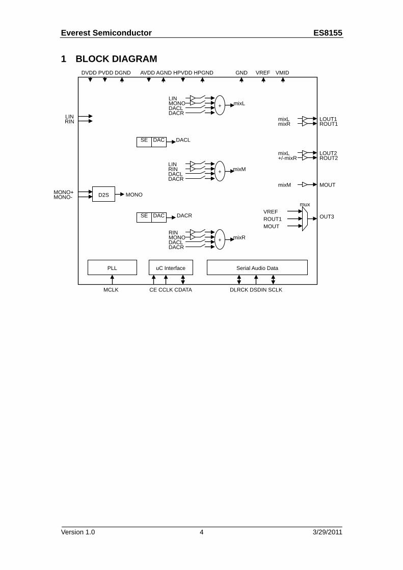
1 BLOCK DIAGRAM
LIN RIN
SE DAC DACL
MONO MONO+ MONO-
SE DAC DACR
mixL + LIN MONO DACL DACR
mixR + RIN MONO DACL DACR
mixM + LIN RIN DACL DACR
mixL mixR
LOUT1 ROUT1
mixL +/-mixR
LOUT2 ROUT2
mixM MOUT
OUT3 VREF ROUT1 MOUT
DVDD PVDD DGND AVDD AGND HPVDD HPGND GND VREF VMID
mux
MCLK
PLL uC Interface
CE CCLK CDATA
Serial Audio Data
DLRCK DSDIN SCLK
D2S
Everest Semiconductor ES8155
Version 1.0 3/29/2011 5
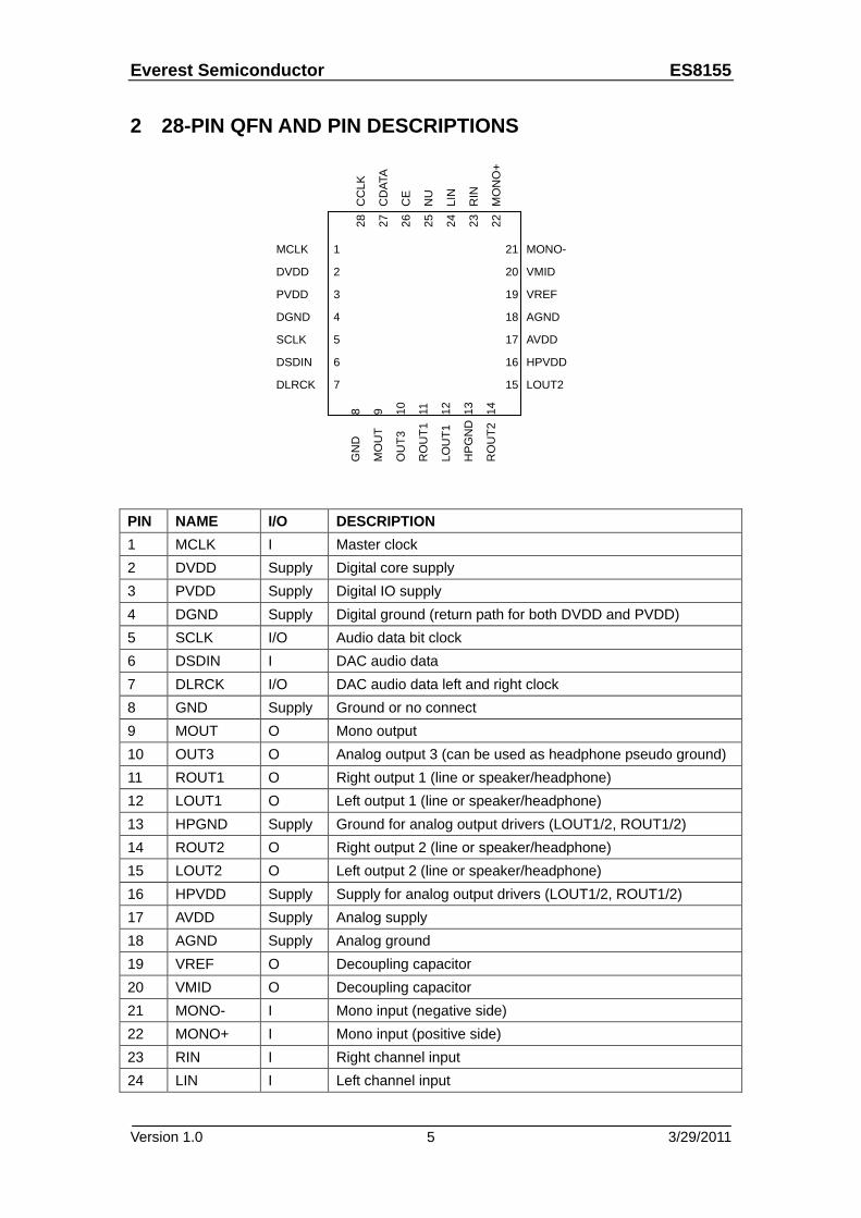
2 28-PIN QFN AND PIN DESCRIPTIONS
PIN NAME I/O DESCRIPTION 1 MCLK I Master clock 2 DVDD Supply Digital core supply 3 PVDD Supply Digital IO supply 4 DGND Supply Digital ground (return path for both DVDD and PVDD) 5 SCLK I/O Audio data bit clock 6 DSDIN I DAC audio data 7 DLRCK I/O DAC audio data left and right clock 8 GND Supply Ground or no connect 9 MOUT O Mono output 10 OUT3 O Analog output 3 (can be used as headphone pseudo ground) 11 ROUT1 O Right output 1 (line or speaker/headphone) 12 LOUT1 O Left output 1 (line or speaker/headphone) 13 HPGND Supply Ground for analog output drivers (LOUT1/2, ROUT1/2) 14 ROUT2 O Right output 2 (line or speaker/headphone) 15 LOUT2 O Left output 2 (line or speaker/headphone) 16 HPVDD Supply Supply for analog output drivers (LOUT1/2, ROUT1/2) 17 AVDD Supply Analog supply 18 AGND Supply Analog ground 19 VREF O Decoupling capacitor 20 VMID O Decoupling capacitor 21 MONO- I Mono input (negative side) 22 MONO+ I Mono input (positive side) 23 RIN I Right channel input 24 LIN I Left channel input
GN
D
MO
UT
OU
T3
RO
UT1
LOU
T1
HP
GN
D
RO
UT2
8 9 10
11
12
13
14
MONO-
VMID
VREF
AGND
AVDD
HPVDD
LOUT2
21
20
19
18
17
16
15
CC
LK
CD
ATA
CE
NU
LIN
RIN
MO
NO
+
28
27
26
25
24
23
22
MCLK
DVDD
PVDD
DGND
SCLK
DSDIN
DLRCK
1
2
3
4
5
6
7
Everest Semiconductor ES8155
Version 1.0 3/29/2011 6
25 NU Not used by chip (arbitrary connection) 26 CE I Control select or device address selection 27 CDATA I/O Control data input or output 28 CCLK I Control clock input
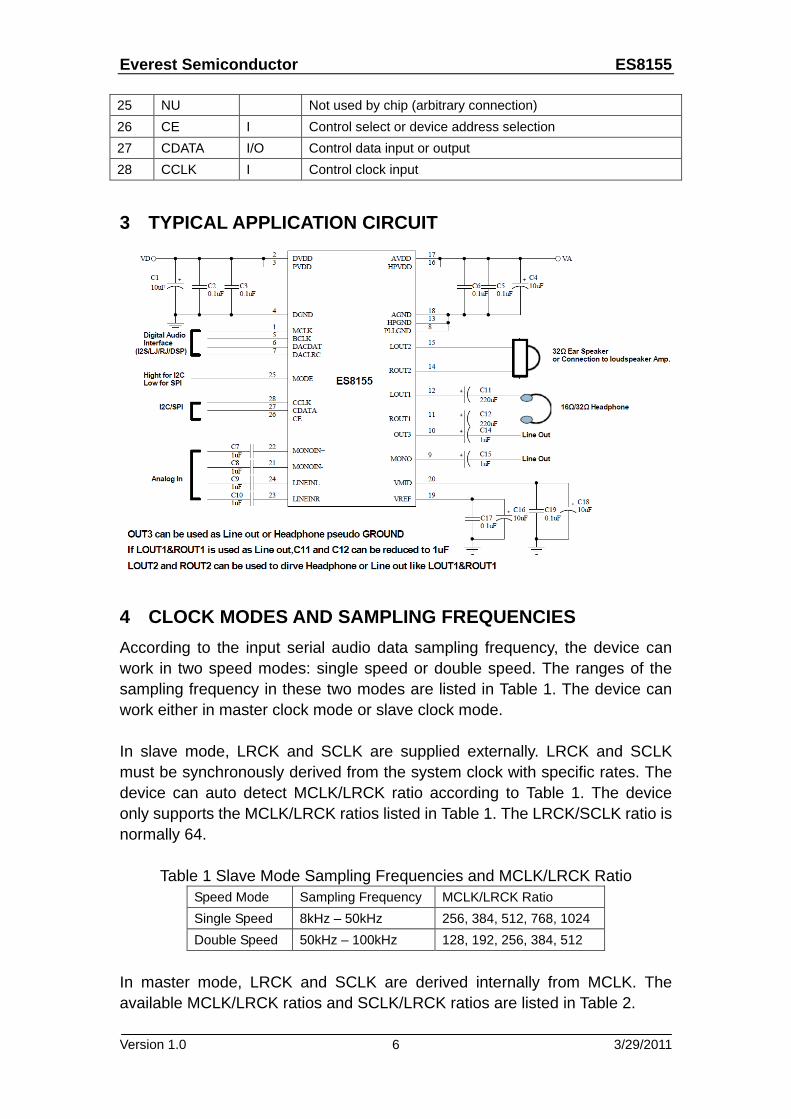
3 TYPICAL APPLICATION CIRCUIT
4 CLOCK MODES AND SAMPLING FREQUENCIES According to the input serial audio data sampling frequency, the device can work in two speed modes: single speed or double speed. The ranges of the sampling frequency in these two modes are listed in Table 1. The device can work either in master clock mode or slave clock mode. In slave mode, LRCK and SCLK are supplied externally. LRCK and SCLK must be synchronously derived from the system clock with specific rates. The device can auto detect MCLK/LRCK ratio according to Table 1. The device only supports the MCLK/LRCK ratios listed in Table 1. The LRCK/SCLK ratio is normally 64.
Table 1 Slave Mode Sampling Frequencies and MCLK/LRCK Ratio Speed Mode Sampling Frequency MCLK/LRCK Ratio Single Speed 8kHz – 50kHz 256, 384, 512, 768, 1024 Double Speed 50kHz – 100kHz 128, 192, 256, 384, 512
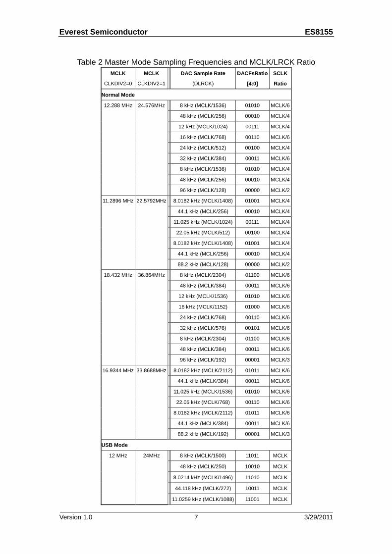
In master mode, LRCK and SCLK are derived internally from MCLK. The available MCLK/LRCK ratios and SCLK/LRCK ratios are listed in Table 2.
Everest Semiconductor ES8155
Version 1.0 3/29/2011 7
Table 2 Master Mode Sampling Frequencies and MCLK/LRCK Ratio
MCLK
CLKDIV2=0
MCLK
CLKDIV2=1
DAC Sample Rate
(DLRCK)
DACFsRatio
[4:0]
SCLK
Ratio
Normal Mode
12.288 MHz 24.576MHz 8 kHz (MCLK/1536) 01010 MCLK/6
48 kHz (MCLK/256) 00010 MCLK/4
12 kHz (MCLK/1024) 00111 MCLK/4
16 kHz (MCLK/768) 00110 MCLK/6
24 kHz (MCLK/512) 00100 MCLK/4
32 kHz (MCLK/384) 00011 MCLK/6
8 kHz (MCLK/1536) 01010 MCLK/4
48 kHz (MCLK/256) 00010 MCLK/4
96 kHz (MCLK/128) 00000 MCLK/2
11.2896 MHz 22.5792MHz 8.0182 kHz (MCLK/1408) 01001 MCLK/4
44.1 kHz (MCLK/256) 00010 MCLK/4
11.025 kHz (MCLK/1024) 00111 MCLK/4
22.05 kHz (MCLK/512) 00100 MCLK/4
8.0182 kHz (MCLK/1408) 01001 MCLK/4
44.1 kHz (MCLK/256) 00010 MCLK/4
88.2 kHz (MCLK/128) 00000 MCLK/2
18.432 MHz 36.864MHz 8 kHz (MCLK/2304) 01100 MCLK/6
48 kHz (MCLK/384) 00011 MCLK/6
12 kHz (MCLK/1536) 01010 MCLK/6
16 kHz (MCLK/1152) 01000 MCLK/6
24 kHz (MCLK/768) 00110 MCLK/6
32 kHz (MCLK/576) 00101 MCLK/6
8 kHz (MCLK/2304) 01100 MCLK/6
48 kHz (MCLK/384) 00011 MCLK/6
96 kHz (MCLK/192) 00001 MCLK/3
16.9344 MHz 33.8688MHz 8.0182 kHz (MCLK/2112) 01011 MCLK/6
44.1 kHz (MCLK/384) 00011 MCLK/6
11.025 kHz (MCLK/1536) 01010 MCLK/6
22.05 kHz (MCLK/768) 00110 MCLK/6
8.0182 kHz (MCLK/2112) 01011 MCLK/6
44.1 kHz (MCLK/384) 00011 MCLK/6
88.2 kHz (MCLK/192) 00001 MCLK/3
USB Mode
12 MHz 24MHz 8 kHz (MCLK/1500) 11011 MCLK
48 kHz (MCLK/250) 10010 MCLK
8.0214 kHz (MCLK/1496) 11010 MCLK
44.118 kHz (MCLK/272) 10011 MCLK
11.0259 kHz (MCLK/1088) 11001 MCLK
Everest Semiconductor ES8155
Version 1.0 3/29/2011 8
12 kHz (MCLK/1000) 11000 MCLK
16 kHz (MCLK/750) 10111 MCLK
22.0588 kHz (MCLK/544) 10110 MCLK
24 kHz (MCLK/500) 10101 MCLK
32 kHz (MCLK/375) 10100* MCLK
8.0214 kHz (MCLK/1496) 11010 MCLK
44.118 kHz (MCLK/272) 10011 MCLK
8 kHz (MCLK/1500) 11011 MCLK
48 kHz (MCLK/250) 10010 MCLK
88.235 kHz (MCLK/136) 10001 MCLK
96 kHz (MCLK/125) 10000 MCLK
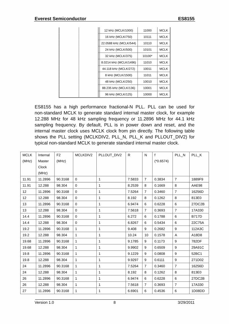
ES8155 has a high performance fractional-N PLL. PLL can be used for non-standard MCLK to generate standard internal master clock, for example 12.288 MHz for 48 kHz sampling frequency or 11.2896 MHz for 44.1 kHz sampling frequency. By default, PLL is in power down and reset, and the internal master clock uses MCLK clock from pin directly. The following table shows the PLL setting (MCLKDIV2, PLL_N, PLL_K and PLLOUT_DIV2) for typical non-standard MCLK to generate standard internal master clock.
MCLK
(MHz)
Internal
Master
Clock
(MHz)
F2
(MHz)
MCLKDIV2 PLLOUT_DIV2 R N f
(*0.6574)
PLL_N PLL_K
11.91 11.2896 90.3168 0 1 7.5833 7 0.3834 7 1889F9
11.91 12.288 98.304 0 1 8.2539 8 0.1669 8 AAE98
12 11.2896 90.3168 0 1 7.5264 7 0.3460 7 16256D
12 12.288 98.304 0 1 8.192 8 0.1262 8 813E0
13 11.2896 90.3168 0 1 6.9474 6 0.6228 6 27DC2B
13 12.288 98.304 0 1 7.5618 7 0.3693 7 17A330
14.4 11.2896 90.3168 0 1 6.272 6 0.1788 6 B717D
14.4 12.288 98.304 0 1 6.8267 6 0.5434 6 22C75A
19.2 11.2896 90.3168 1 1 9.408 9 0.2682 9 112A3C
19.2 12.288 98.304 1 1 10.24 10 0.1578 A A18D8
19.68 11.2896 90.3168 1 1 9.1785 9 0.1173 9 782DF
19.68 12.288 98.304 1 1 9.9902 9 0.6509 9 29A91C
19.8 11.2896 90.3168 1 1 9.1229 9 0.0808 9 52BC1
19.8 12.288 98.304 1 1 9.9297 9 0.6111 9 271D02
24 11.2896 90.3168 1 1 7.5264 7 0.3460 7 16256D
24 12.288 98.304 1 1 8.192 8 0.1262 8 813E0
26 11.2896 90.3168 1 1 6.9474 6 0.6228 6 27DC2B
26 12.288 98.304 1 1 7.5618 7 0.3693 7 17A330
27 11.2896 90.3168 1 1 6.6901 6 0.4536 6 1D08DD
Everest Semiconductor ES8155
Version 1.0 3/29/2011 9
27 12.288 98.304 1 1 7.2818 7 0.1852 7 BDACC
5 MICRO-CONTROLLER CONFIGURATION INTERFACE The device supports standard SPI and 2-wire micro-controller configuration interface. External micro-controller can completely configure the device through writing to internal configuration registers. Please see section 8 for the details of configuration register definition. The identical device pins are used to configure either SPI or 2-wire interface. In SPI mode, pin CE, CCLK and CDATA function as SPI_CSn, SPI_CLK and SPI_DIN. In 2-wire mode, pin CE, CCLK and CDATA function as AD0, SCL and SDA. To select SPI mode, apply high to low transition signal to CE pin. Otherwise the device will operate in 2-wire interface mode.
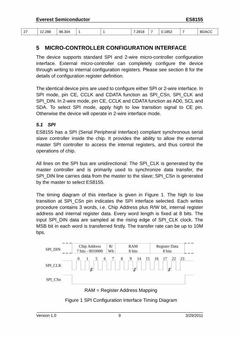
5.1 SPI ES8155 has a SPI (Serial Peripheral Interface) compliant synchronous serial slave controller inside the chip. It provides the ability to allow the external master SPI controller to access the internal registers, and thus control the operations of chip. All lines on the SPI bus are unidirectional: The SPI_CLK is generated by the master controller and is primarily used to synchronize data transfer, the SPI_DIN line carries data from the master to the slave; SPI_CSn is generated by the master to select ES8155. The timing diagram of this interface is given in Figure 1. The high to low transition at SPI_CSn pin indicates the SPI interface selected. Each writes procedure contains 3 words, i.e. Chip Address plus R/W bit, internal register address and internal register data. Every word length is fixed at 8 bits. The input SPI_DIN data are sampled at the rising edge of SPI_CLK clock. The MSB bit in each word is transferred firstly. The transfer rate can be up to 10M bps.
Chip Address7 bits - 0010000
0
SPI_DIN
SPI_CLK
SPI_CSn
1
R/Wb
5 6 7 8 9 14 15 16 17 22 23
RAM8 bits
Register Data8 bits
Figure 1 SPI Configuration Interface Timing Diagram
RAM = Register Address Mapping
Everest Semiconductor ES8155
Version 1.0 3/29/2011 10
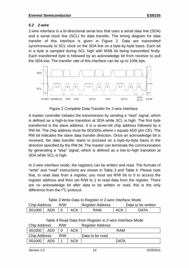
5.2 2-wire 2-wire interface is a bi-directional serial bus that uses a serial data line (SDA) and a serial clock line (SCL) for data transfer. The timing diagram for data transfer of this interface is given in Figure 2. Data are transmitted synchronously to SCL clock on the SDA line on a byte-by-byte basis. Each bit in a byte is sampled during SCL high with MSB bit being transmitted firstly. Each transferred byte is followed by an acknowledge bit from receiver to pull the SDA low. The transfer rate of this interface can be up to 100k bps.
A master controller initiates the transmission by sending a “start” signal, which is defined as a high-to-low transition at SDA while SCL is high. The first byte transferred is the slave address. It is a seven-bit chip address followed by a RW bit. The chip address must be 001000x,where x equals AD0 (pin CE). The RW bit indicates the slave data transfer direction. Once an acknowledge bit is received, the data transfer starts to proceed on a byte-by-byte basis in the direction specified by the RW bit. The master can terminate the communication by generating a “stop” signal, which is defined as a low-to-high transition at SDA while SCL is high. In 2-wire interface mode, the registers can be written and read. The formats of “write” and “read” instructions are shown in Table 3 and Table 4. Please note that, to read data from a register, you must set R/W bit to 0 to access the register address and then set R/W to 1 to read data from the register. There are no acknowledge bit after data to be written or read, this is the only difference from the I2C protocol.
Table 3 Write Data to Register in 2-wire Interface Mode Chip Address R/W Register Address Data to be written 001000 AD0 0 ACK RAM ACK DATA
Table 4 Read Data from Register in 2-wire Interface Mode
Chip Address R/W Register Address 001000 AD0 0 ACK RAM Chip Address R/W Data to be read 001000 AD0 1 ACK DATA
Figure 2 Complete Data Transfer for 2-wire Interface
Everest Semiconductor ES8155
Version 1.0 3/29/2011 11
6 CONFIGURATION REGISTER DEFINITION SPI and 2-wire configuration interface share the same registers because there is only one interface active at any time. There are total of 61 user programmable 8-bit registers in this device. These registers control the operations of DAC. External master controller can access these registers by using the slave address specified in RAM (Register Address Map) register as shown in the Table 5.
Everest Semiconductor ES8155
Version 1.0 3/29/2011 12
Table 5 Bit Content of Register Address Map
Adr Name Bit7 Bit6 Bit5 Bit4 Bit3 Bit2 Bit1 Bit0 default
0
Output
Setting
LOUT1 Volume LP_OUT1 PDN_LOUT1 LOUT1VOL 40
1 ROUT1 Volume PDN_ROUT1 ROUT1VOL 40
2 LOUT2 Volume LP_OUT2 PDN_LOUT2 LOUT2VOL 40
3 ROUT2 Volume PDN_ROUT2 ROUT2VOL 40
4 MOUT Volume LP_MOUT PDN_MOUT MOUTVOL 40
5 OUT Control 1 LP_OUT3 PDN_OUT3 OUT3SW LP_ROUT2INV ROUT2INV 40
6 OUT Control 2 L2R2BOTH L1R1BOTH 00
7
Mixer
Setting
Left Mixer LI2LOMU LI2LOVOL MI2LOMU MI2LOVOL FF
8 Right Mixer MI2ROMU RI2ROVOL RI2ROMU MI2ROVOL FF
9 Mono Mixer LI2MOMU LI2MOVOL RI2MOMU RI2MOVOL FF
A DAC to Mixer PDN_MONODIFF DMEN LD2MOMU RD2MOMU LD2LOMU RD2LOMU LD2ROMU RD2ROMU BF
B Mixer LP mode LP_MONODIFF LP_MMIX LP_LMIX LP_RMIX 00
C
DAC
Setting
Left DAC Volume DACLVOL C0
D Right DAC Volume DACRVOL C0
E DAC Control LP_DACL PDN_DACL LP_DACR PDN_DACR DACLMU DACRMU 55
F DAC Control AUTOMUTE CLICKFREE VPPSCALE DACLRBOTH DACSOFTRAMP DACRAMPRATE C4
10 DAC Control DACINVL DACINVR DACTOEN DACDAT 08
11 DAC Control DACZEROL DACZEROR DACMONO DACSE 00
12
Shelving1_A
SHV1_A[29:24] 1F
13 SHV1_A[23:16] F7
14 SHV1_A[15:8] FD
15 SHV1_A[7:0] FF
Everest Semiconductor ES8155
Version 1.0 3/29/2011 13
16
Shelving1_B
SHV1_B[29:24] 1F
17 SHV1_B[23:16] F7
18 SHV1_B[15:8] FD
19 SHV1_B[7:0] FF
1A
Shelving2_A
SHV2_A[29:24] 1F
1B SHV2_A[23:16] F7
1C SHV2_A[15:8] FD
1D SHV2_A[7:0] FF
1E
Shelving2_B
SHV2_B[29:24] 1F
1F SHV2_B[23:16] F7
20 SHV2_B[15:8] FD
21 SHV2_B[7:0] FF
22
Shelving3_A
SHV3_A[29:24] 1F
23 SHV3_A[23:16] F7
24 SHV3_A[15:8] FD
25 SHV3_A[7:0] FF
26
Shelving3_B
SHV3_B[29:24] 1F
27 SHV3_B[23:16] F7
28 SHV3_B[15:8] FD
29 SHV3_B[7:0] FF
2A Digital
Audio
I/F
Setting
Digital Interface DACFORMAT DACLRSWP DACLRP DACWL 00
2B Digital Interface MCLKDIV2 SCLKINV FSMODE DACMSC 01
2C Sample Rate DACSR 06
2D SCLK Divider SCLKDIV 00
2E Reference Reset RST_CP 00
Everest Semiconductor ES8155
Version 1.0 3/29/2011 14
2F Setting Power Down PDN_ANA PDN_DIG PDN_FSM PDN_DLL 0C
30 Reference SEQEN 00
31 Reference ENREFR VROI VMIDSEL VMIDLOW 28
32 Reference PDN_VREFGEN PDN_IBIASGEN LP_DACVRP LP_VREFBUF PDN_VREFBUF VREFR_LO 34
33 Reference IBIASSW VSEL FC
34 Reference MOUT_REF2 MOUT_REF1 OUT3_REF2 OUT3_REF1 OUT2_REF2 OUT2_REF1 OUT1_REF2 OUT1_REF1 55
35 Reference MONO_REF2 MONO_REF1 MIX_REF2 MIX_REF1 05
36
PLL
Setting
PLL Control pdn cp2 cp1 cp0 SupSel1 SupSel0 kvco1 kvco0 08
37 PLL Control LP MCLKSEL PLLOUT_DIV2 PLL_RB PLL_EN 00
38 PLL Control DITH_MAG PLL_N 00
39 PLL Control PLL_K[21:16] 00
3A PLL Control PLL_K[15:8] 00
3B PLL Control PLL_K[7:0] 00
Everest Semiconductor ES8155
Version 1.0 3/29/2011 15
6.1 Output Setting 6.1.1 Register 0x00 – LOUT1 Volume, Default 0100 0000
Bit Name Bit Description LP_LOUT1 7 0 – normal (default)
1 – low power setting for LOUT1 PDN_LOUT1 6 0 – not power down
1 – power down LOUT1 (default) LOUT1VOL 5:0 LOUT1 volume control
000000 – -45 dB (default) 000001 – -43.5 dB 000010 – -42 dB … 011110 – 0 dB 011111 – 1.5 dB … 100000 – 3 dB
6.1.2 Register 0x01 – ROUT1 Volume, Default 0100 0000
Bit Name Bit Description LP_ROUT1 7 0 – normal (default)
1 – low power setting for ROUT1 PDN_ROUT1 6 0 – not power down
1 – power down ROUT1 (default) ROUT1VOL 5:0 ROUT1 volume control
000000 – -45 dB (default) 000001 – -43.5 dB 000010 – -42 dB … 011110 – 0 dB 011111 – 1.5 dB … 100000 – 3 dB
6.1.3 Register 0x02 – LOUT2 Volume, Default 0100 0000
Bit Name Bit Description LP_LOUT2 7 0 – normal (default)
1 – low power setting for LOUT2 PDN_LOUT2 6 0 – not power down
1 – power down LOUT2 (default) LOUT2VOL 5:0 LOUT2 volume control
000000 – -45 dB (default) 000001 – -43.5 dB
Everest Semiconductor ES8155
Version 1.0 3/29/2011 16
000010 – -42 dB … 011110 – 0 dB 011111 – 1.5 dB … 100000 – 3 dB
6.1.4 Register 0x03 – ROUT2 Volume, Default 0100 0000
Bit Name Bit Description LP_ROUT2 7 0 – normal (default)
1 – low power setting for ROUT2 PDN_ROUT2 6 0 – not power down
1 – power down ROUT2 (default) ROUT2VOL 5:0 ROUT2 volume control
000000 – -45 dB (default) 000001 – -43.5 dB 000010 – -42 dB … 011110 – 0 dB 011111 – 1.5 dB … 100000 – 3 dB
6.1.5 Register 0x04 – MOUT Volume, Default 0100 0000
Bit Name Bit Description LP_MOUT 7 0 – normal (default)
1 – low power setting for Mono Out PDN_MOUT 6 0 – not power down
1 – power down mono out (default) MOUTVOL 5:0 Mono Out volume control
000000 – -45 dB (default) 000001 – -43.5 dB 000010 – -42 dB … 011110 – 0 dB 011111 – 1.5 dB … 100000 – 3 dB
6.1.6 Register 0x05 – Out Control 1, Default 0100 0000
Bit Name Bit Description LP_OUT3 7 0 – normal (default)
1 – low power setting for OUT3 PDN_OUT3 6 0 – not power down
Everest Semiconductor ES8155
Version 1.0 3/29/2011 17
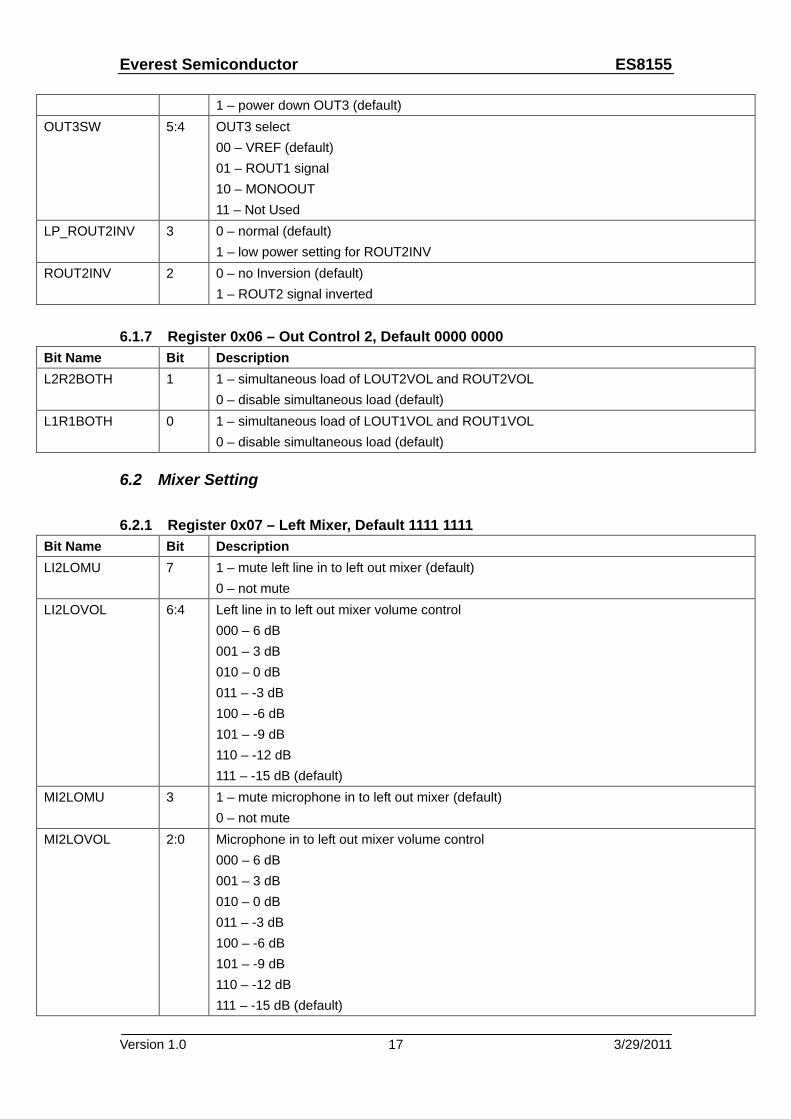
1 – power down OUT3 (default) OUT3SW 5:4 OUT3 select
00 – VREF (default) 01 – ROUT1 signal 10 – MONOOUT 11 – Not Used
LP_ROUT2INV 3 0 – normal (default) 1 – low power setting for ROUT2INV
ROUT2INV 2 0 – no Inversion (default) 1 – ROUT2 signal inverted
6.1.7 Register 0x06 – Out Control 2, Default 0000 0000
Bit Name Bit Description L2R2BOTH 1 1 – simultaneous load of LOUT2VOL and ROUT2VOL
0 – disable simultaneous load (default) L1R1BOTH 0 1 – simultaneous load of LOUT1VOL and ROUT1VOL
0 – disable simultaneous load (default)
6.2 Mixer Setting 6.2.1 Register 0x07 – Left Mixer, Default 1111 1111
Bit Name Bit Description LI2LOMU 7 1 – mute left line in to left out mixer (default)
0 – not mute LI2LOVOL 6:4 Left line in to left out mixer volume control
000 – 6 dB 001 – 3 dB 010 – 0 dB 011 – -3 dB 100 – -6 dB 101 – -9 dB 110 – -12 dB 111 – -15 dB (default)
MI2LOMU 3 1 – mute microphone in to left out mixer (default) 0 – not mute
MI2LOVOL 2:0 Microphone in to left out mixer volume control 000 – 6 dB 001 – 3 dB 010 – 0 dB 011 – -3 dB 100 – -6 dB 101 – -9 dB 110 – -12 dB 111 – -15 dB (default)
Everest Semiconductor ES8155
Version 1.0 3/29/2011 18
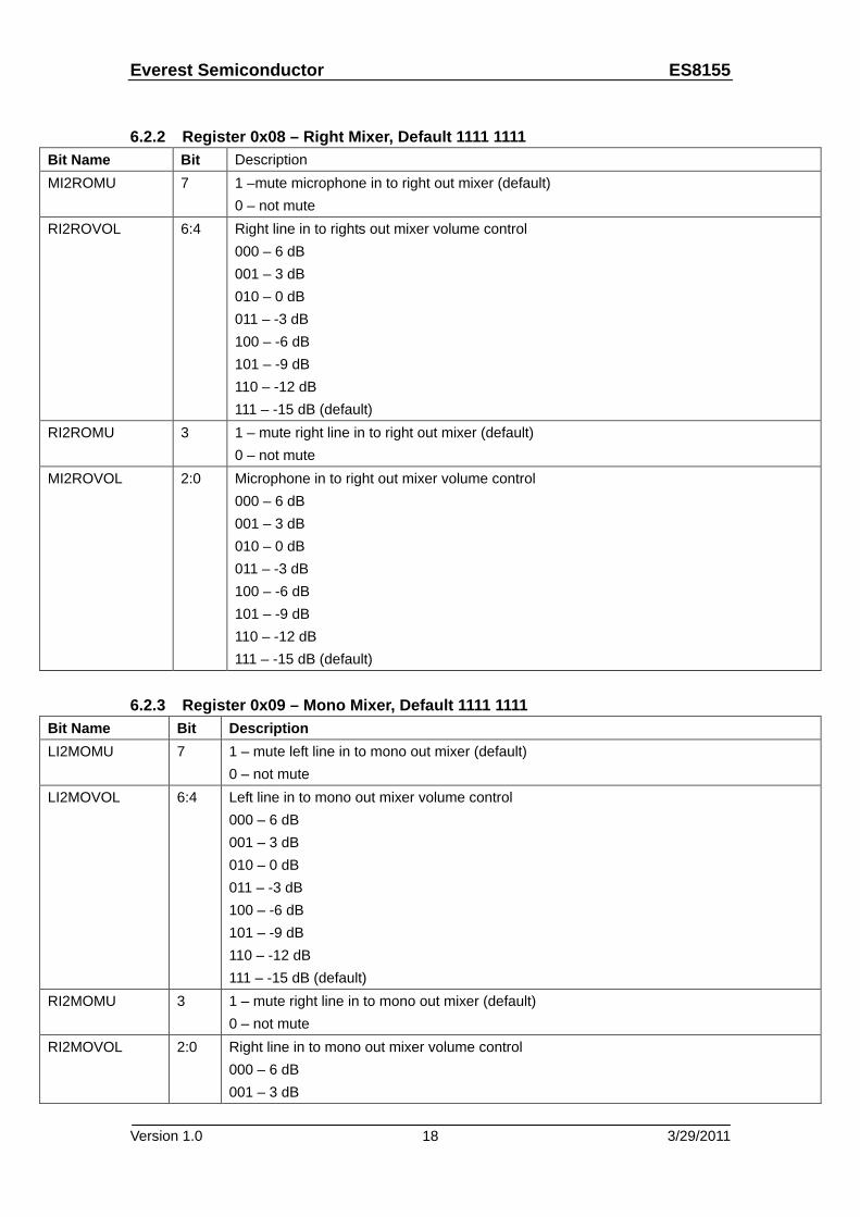
6.2.2 Register 0x08 – Right Mixer, Default 1111 1111
Bit Name Bit Description MI2ROMU 7 1 –mute microphone in to right out mixer (default)
0 – not mute RI2ROVOL 6:4 Right line in to rights out mixer volume control
000 – 6 dB 001 – 3 dB 010 – 0 dB 011 – -3 dB 100 – -6 dB 101 – -9 dB 110 – -12 dB 111 – -15 dB (default)
RI2ROMU 3 1 – mute right line in to right out mixer (default) 0 – not mute
MI2ROVOL 2:0 Microphone in to right out mixer volume control 000 – 6 dB 001 – 3 dB 010 – 0 dB 011 – -3 dB 100 – -6 dB 101 – -9 dB 110 – -12 dB 111 – -15 dB (default)
6.2.3 Register 0x09 – Mono Mixer, Default 1111 1111
Bit Name Bit Description LI2MOMU 7 1 – mute left line in to mono out mixer (default)
0 – not mute LI2MOVOL 6:4 Left line in to mono out mixer volume control
000 – 6 dB 001 – 3 dB 010 – 0 dB 011 – -3 dB 100 – -6 dB 101 – -9 dB 110 – -12 dB 111 – -15 dB (default)
RI2MOMU 3 1 – mute right line in to mono out mixer (default) 0 – not mute
RI2MOVOL 2:0 Right line in to mono out mixer volume control 000 – 6 dB 001 – 3 dB
Everest Semiconductor ES8155
Version 1.0 3/29/2011 19
010 – 0 dB 011 – -3 dB 100 – -6 dB 101 – -9 dB 110 – -12 dB 111 – -15 dB (default)
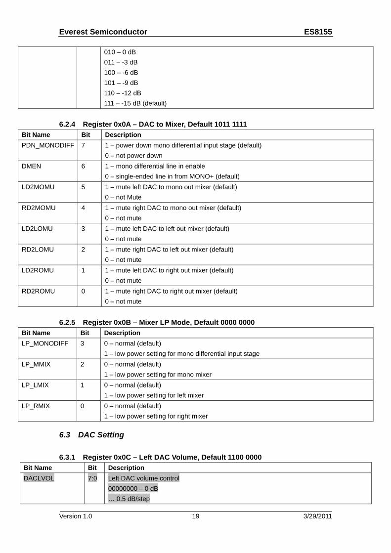
6.2.4 Register 0x0A – DAC to Mixer, Default 1011 1111
Bit Name Bit Description PDN_MONODIFF 7 1 – power down mono differential input stage (default)
0 – not power down DMEN 6 1 – mono differential line in enable
0 – single-ended line in from MONO+ (default) LD2MOMU 5 1 – mute left DAC to mono out mixer (default)
0 – not Mute RD2MOMU 4 1 – mute right DAC to mono out mixer (default)
0 – not mute LD2LOMU 3 1 – mute left DAC to left out mixer (default)
0 – not mute RD2LOMU 2 1 – mute right DAC to left out mixer (default)
0 – not mute LD2ROMU 1 1 – mute left DAC to right out mixer (default)
0 – not mute RD2ROMU 0 1 – mute right DAC to right out mixer (default)
0 – not mute 6.2.5 Register 0x0B – Mixer LP Mode, Default 0000 0000
Bit Name Bit Description LP_MONODIFF 3 0 – normal (default)
1 – low power setting for mono differential input stage LP_MMIX 2 0 – normal (default)
1 – low power setting for mono mixer LP_LMIX 1 0 – normal (default)
1 – low power setting for left mixer LP_RMIX 0 0 – normal (default)
1 – low power setting for right mixer
6.3 DAC Setting 6.3.1 Register 0x0C – Left DAC Volume, Default 1100 0000
Bit Name Bit Description DACLVOL 7:0 Left DAC volume control
00000000 – 0 dB … 0.5 dB/step
Everest Semiconductor ES8155
Version 1.0 3/29/2011 20
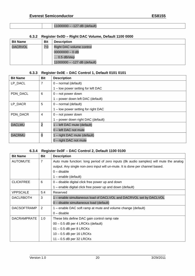
11000000 – -127 dB (default) 6.3.2 Register 0x0D – Right DAC Volume, Default 1100 0000
Bit Name Bit Description DACRVOL 7:0 Right DAC volume control
00000000 – 0 dB … 0.5 dB/step 11000000 – -127 dB (default)
6.3.3 Register 0x0E – DAC Control 1, Default 0101 0101
Bit Name Bit Description LP_DACL 7 0 – normal (default)
1 – low power setting for left DAC PDN_DACL 6 0 – not power down
1 – power down left DAC (default) LP_DACR 5 0 – normal (default)
1 – low power setting for right DAC PDN_DACR 4 0 – not power down
1 – power down right DAC (default) DACLMU 2 1 – left DAC mute (default)
0 – left DAC not mute DACRMU 0 1 – right DAC mute (default)
0 – right DAC not mute 6.3.4 Register 0x0F – DAC Control 2, Default 1100 0100
Bit Name Bit Description AUTOMUTE 7 Auto mute function: long period of zero inputs (8k audio samples) will mute the analog
output. Any single non-zero input will un-mute. It is done per channel based. 0 – disable 1 – enable (default)
CLICKFREE 6 0 – disable digital click free power up and down 1 – enable digital click free power up and down (default)
VPPSCALE 5:4 Reserved DACLRBOTH 3 1 – enable simultaneous load of DACLVOL and DACRVOL set by DACLVOL
0 – disable simultaneous load (default) DACSOFTRAMP 2 1 – enable DAC soft ramp at mute and volume change (default)
0 – disable DACRAMPRATE 1:0 These bits define DAC gain control ramp rate
00 – 0.5 dB per 4 LRCKs (default) 01 – 0.5 dB per 8 LRCKs 10 – 0.5 dB per 16 LRCKs 11 – 0.5 dB per 32 LRCKs
Everest Semiconductor ES8155
Version 1.0 3/29/2011 21
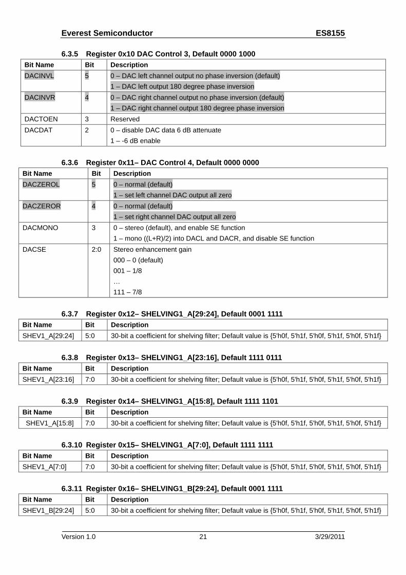
6.3.5 Register 0x10 DAC Control 3, Default 0000 1000 Bit Name Bit Description DACINVL 5 0 – DAC left channel output no phase inversion (default)
1 – DAC left output 180 degree phase inversion DACINVR 4 0 – DAC right channel output no phase inversion (default)
1 – DAC right channel output 180 degree phase inversion DACTOEN 3 Reserved DACDAT 2 0 – disable DAC data 6 dB attenuate
1 – -6 dB enable 6.3.6 Register 0x11– DAC Control 4, Default 0000 0000
Bit Name Bit Description DACZEROL 5 0 – normal (default)
1 – set left channel DAC output all zero DACZEROR 4 0 – normal (default)
1 – set right channel DAC output all zero DACMONO 3 0 – stereo (default), and enable SE function
1 – mono ((L+R)/2) into DACL and DACR, and disable SE function DACSE 2:0 Stereo enhancement gain
000 – 0 (default) 001 – 1/8 … 111 – 7/8
6.3.7 Register 0x12– SHELVING1_A[29:24], Default 0001 1111
Bit Name Bit Description SHEV1_A[29:24] 5:0 30-bit a coefficient for shelving filter; Default value is 5'h0f, 5'h1f, 5'h0f, 5'h1f, 5'h0f, 5'h1f
6.3.8 Register 0x13– SHELVING1_A[23:16], Default 1111 0111
Bit Name Bit Description SHEV1_A[23:16] 7:0 30-bit a coefficient for shelving filter; Default value is 5'h0f, 5'h1f, 5'h0f, 5'h1f, 5'h0f, 5'h1f
6.3.9 Register 0x14– SHELVING1_A[15:8], Default 1111 1101
Bit Name Bit Description SHEV1_A[15:8] 7:0 30-bit a coefficient for shelving filter; Default value is 5'h0f, 5'h1f, 5'h0f, 5'h1f, 5'h0f, 5'h1f
6.3.10 Register 0x15– SHELVING1_A[7:0], Default 1111 1111
Bit Name Bit Description SHEV1_A[7:0] 7:0 30-bit a coefficient for shelving filter; Default value is 5'h0f, 5'h1f, 5'h0f, 5'h1f, 5'h0f, 5'h1f
6.3.11 Register 0x16– SHELVING1_B[29:24], Default 0001 1111
Bit Name Bit Description SHEV1_B[29:24] 5:0 30-bit a coefficient for shelving filter; Default value is 5'h0f, 5'h1f, 5'h0f, 5'h1f, 5'h0f, 5'h1f
Everest Semiconductor ES8155
Version 1.0 3/29/2011 22
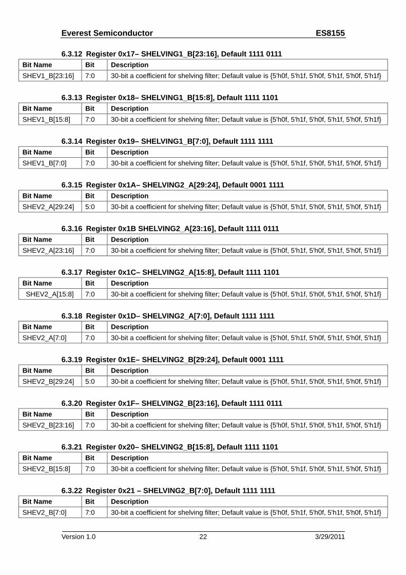
6.3.12 Register 0x17– SHELVING1_B[23:16], Default 1111 0111 Bit Name Bit Description SHEV1_B[23:16] 7:0 30-bit a coefficient for shelving filter; Default value is 5'h0f, 5'h1f, 5'h0f, 5'h1f, 5'h0f, 5'h1f
6.3.13 Register 0x18– SHELVING1_B[15:8], Default 1111 1101
Bit Name Bit Description SHEV1_B[15:8] 7:0 30-bit a coefficient for shelving filter; Default value is 5'h0f, 5'h1f, 5'h0f, 5'h1f, 5'h0f, 5'h1f
6.3.14 Register 0x19– SHELVING1_B[7:0], Default 1111 1111
Bit Name Bit Description SHEV1_B[7:0] 7:0 30-bit a coefficient for shelving filter; Default value is 5'h0f, 5'h1f, 5'h0f, 5'h1f, 5'h0f, 5'h1f
6.3.15 Register 0x1A– SHELVING2_A[29:24], Default 0001 1111
Bit Name Bit Description SHEV2_A[29:24] 5:0 30-bit a coefficient for shelving filter; Default value is 5'h0f, 5'h1f, 5'h0f, 5'h1f, 5'h0f, 5'h1f
6.3.16 Register 0x1B SHELVING2_A[23:16], Default 1111 0111
Bit Name Bit Description SHEV2_A[23:16] 7:0 30-bit a coefficient for shelving filter; Default value is 5'h0f, 5'h1f, 5'h0f, 5'h1f, 5'h0f, 5'h1f
6.3.17 Register 0x1C– SHELVING2_A[15:8], Default 1111 1101
Bit Name Bit Description SHEV2_A[15:8] 7:0 30-bit a coefficient for shelving filter; Default value is 5'h0f, 5'h1f, 5'h0f, 5'h1f, 5'h0f, 5'h1f
6.3.18 Register 0x1D– SHELVING2_A[7:0], Default 1111 1111
Bit Name Bit Description SHEV2_A[7:0] 7:0 30-bit a coefficient for shelving filter; Default value is 5'h0f, 5'h1f, 5'h0f, 5'h1f, 5'h0f, 5'h1f
6.3.19 Register 0x1E– SHELVING2_B[29:24], Default 0001 1111
Bit Name Bit Description SHEV2_B[29:24] 5:0 30-bit a coefficient for shelving filter; Default value is 5'h0f, 5'h1f, 5'h0f, 5'h1f, 5'h0f, 5'h1f
6.3.20 Register 0x1F– SHELVING2_B[23:16], Default 1111 0111
Bit Name Bit Description SHEV2_B[23:16] 7:0 30-bit a coefficient for shelving filter; Default value is 5'h0f, 5'h1f, 5'h0f, 5'h1f, 5'h0f, 5'h1f
6.3.21 Register 0x20– SHELVING2_B[15:8], Default 1111 1101
Bit Name Bit Description SHEV2_B[15:8] 7:0 30-bit a coefficient for shelving filter; Default value is 5'h0f, 5'h1f, 5'h0f, 5'h1f, 5'h0f, 5'h1f
6.3.22 Register 0x21 – SHELVING2_B[7:0], Default 1111 1111
Bit Name Bit Description SHEV2_B[7:0] 7:0 30-bit a coefficient for shelving filter; Default value is 5'h0f, 5'h1f, 5'h0f, 5'h1f, 5'h0f, 5'h1f
Everest Semiconductor ES8155
Version 1.0 3/29/2011 23
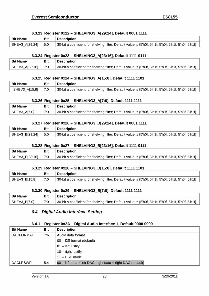
6.3.23 Register 0x22 – SHELVING3_A[29:24], Default 0001 1111
Bit Name Bit Description SHEV3_A[29:24] 5:0 30-bit a coefficient for shelving filter; Default value is 5'h0f, 5'h1f, 5'h0f, 5'h1f, 5'h0f, 5'h1f
6.3.24 Register 0x23 – SHELVING3_A[23:16], Default 1111 0111
Bit Name Bit Description SHEV3_A[23:16] 7:0 30-bit a coefficient for shelving filter; Default value is 5'h0f, 5'h1f, 5'h0f, 5'h1f, 5'h0f, 5'h1f
6.3.25 Register 0x24 – SHELVING3_A[15:8], Default 1111 1101
Bit Name Bit Description SHEV3_A[15:8] 7:0 30-bit a coefficient for shelving filter; Default value is 5'h0f, 5'h1f, 5'h0f, 5'h1f, 5'h0f, 5'h1f
6.3.26 Register 0x25 – SHELVING3_A[7:0], Default 1111 1111
Bit Name Bit Description SHEV3_A[7:0] 7:0 30-bit a coefficient for shelving filter; Default value is 5'h0f, 5'h1f, 5'h0f, 5'h1f, 5'h0f, 5'h1f
6.3.27 Register 0x26 – SHELVING3_B[29:24], Default 0001 1111
Bit Name Bit Description SHEV3_B[29:24] 5:0 30-bit a coefficient for shelving filter; Default value is 5'h0f, 5'h1f, 5'h0f, 5'h1f, 5'h0f, 5'h1f
6.3.28 Register 0x27 – SHELVING3_B[23:16], Default 1111 0111
Bit Name Bit Description SHEV3_B[23:16] 7:0 30-bit a coefficient for shelving filter; Default value is 5'h0f, 5'h1f, 5'h0f, 5'h1f, 5'h0f, 5'h1f
6.3.29 Register 0x28 – SHELVING3_B[15:8], Default 1111 1101
Bit Name Bit Description SHEV3_B[15:8] 7:0 30-bit a coefficient for shelving filter; Default value is 5'h0f, 5'h1f, 5'h0f, 5'h1f, 5'h0f, 5'h1f
6.3.30 Register 0x29 – SHELVING3_B[7:0], Default 1111 1111
Bit Name Bit Description SHEV3_B[7:0] 7:0 30-bit a coefficient for shelving filter; Default value is 5'h0f, 5'h1f, 5'h0f, 5'h1f, 5'h0f, 5'h1f
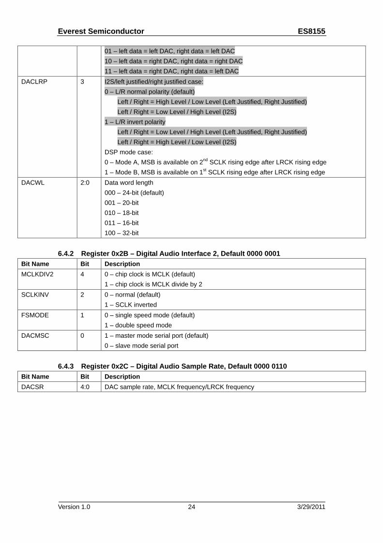
6.4 Digital Audio Interface Setting 6.4.1 Register 0x2A – Digital Audio Interface 1, Default 0000 0000
Bit Name Bit Description DACFORMAT 7:6 Audio data format
00 – I2S format (default) 01 – left justify 10 – right justify, 11 – DSP mode
DACLRSWP 5:4 00 – left data = left DAC, right data = right DAC (default)
Everest Semiconductor ES8155
Version 1.0 3/29/2011 24
01 – left data = left DAC, right data = left DAC 10 – left data = right DAC, right data = right DAC 11 – left data = right DAC, right data = left DAC
DACLRP 3 I2S/left justified/right justified case: 0 – L/R normal polarity (default)
Left / Right = High Level / Low Level (Left Justified, Right Justified) Left / Right = Low Level / High Level (I2S)
1 – L/R invert polarity Left / Right = Low Level / High Level (Left Justified, Right Justified) Left / Right = High Level / Low Level (I2S)
DSP mode case: 0 – Mode A, MSB is available on 2nd SCLK rising edge after LRCK rising edge 1 – Mode B, MSB is available on 1st SCLK rising edge after LRCK rising edge
DACWL 2:0 Data word length 000 – 24-bit (default) 001 – 20-bit 010 – 18-bit 011 – 16-bit 100 – 32-bit
6.4.2 Register 0x2B – Digital Audio Interface 2, Default 0000 0001
Bit Name Bit Description MCLKDIV2 4 0 – chip clock is MCLK (default)
1 – chip clock is MCLK divide by 2 SCLKINV 2 0 – normal (default)
1 – SCLK inverted FSMODE 1 0 – single speed mode (default)
1 – double speed mode DACMSC 0 1 – master mode serial port (default)
0 – slave mode serial port 6.4.3 Register 0x2C – Digital Audio Sample Rate, Default 0000 0110
Bit Name Bit Description DACSR 4:0 DAC sample rate, MCLK frequency/LRCK frequency
Everest Semiconductor ES8155
Version 1.0 3/29/2011 25
00000 – 128 00001 – 192 00010 – 256 00011 – 384 00100 – 512 00101 – 576 00110 – 768 (default) 00111 – 1024 01000 – 1152 01001 – 1408 01010 – 1536 01011 – 2112 01100 – 2304
10000 – 125 10001 – 136 10010 – 250 10011 – 272 10100 – 375 10101 – 500 10110 – 544 10111 – 750 11000 – 1000 11001 – 1088 11010 – 1496 11011 – 1500 Other – Reserved
6.4.4 Register 0x2D – SCLK Divider, Default 0000 0000
Bit Name Bit Description SCLKDIV 4:0 SCLK divider
0 – divide depend on DACSR and clock frequency 1 – divide by 1 2 – divide by 2 3 – divide by 3 4 – divide by 4 5 – divide by 6 6 – divide by 8 7 – divide by 9 8 – divide by 11 9 –divide by 12 10 – divide by 16 11 – divide by 18 12 – divide by 22 13 – divide by 24 14 – divide by 33 15 – divide by 36 16 – divide by 44 17 – divide by 48 18 – divide by 66 19 – divide by 72 other – divide by 4
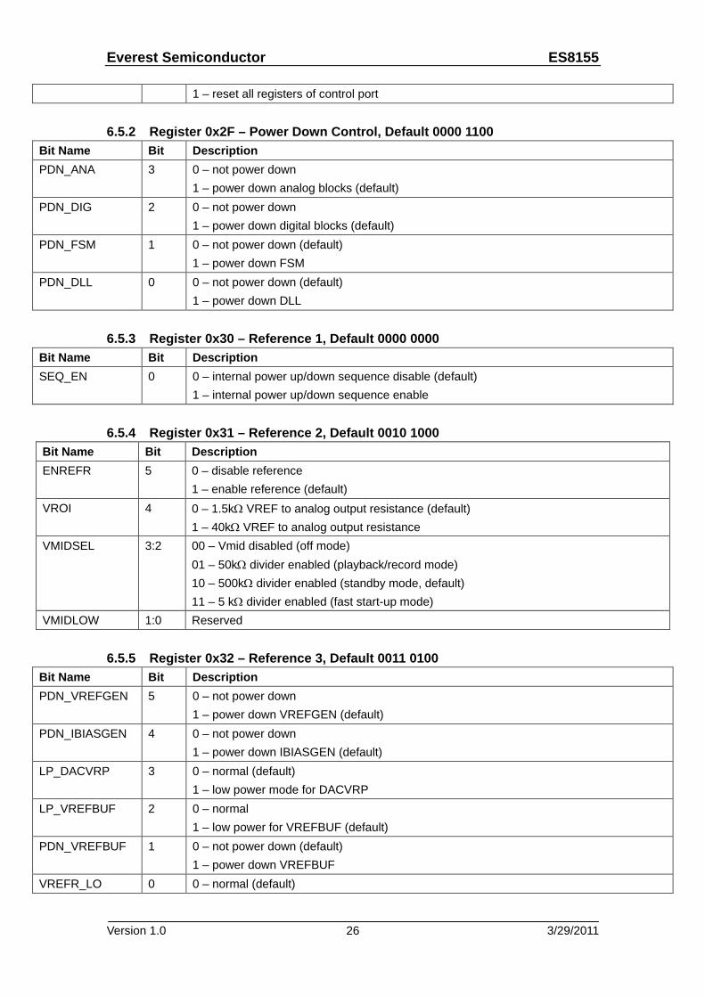
6.5 Reference Setting 6.5.1 Register 0x2E – Control Port Registers Reset, Default 0000 0000
Bit Name Bit Description RST_CP 7 0 – not reset (default)
Everest Semiconductor ES8155
Version 1.0 3/29/2011 26
1 – reset all registers of control port 6.5.2 Register 0x2F – Power Down Control, Default 0000 1100
Bit Name Bit Description PDN_ANA 3 0 – not power down
1 – power down analog blocks (default) PDN_DIG 2 0 – not power down
1 – power down digital blocks (default) PDN_FSM 1 0 – not power down (default)
1 – power down FSM PDN_DLL 0 0 – not power down (default)
1 – power down DLL 6.5.3 Register 0x30 – Reference 1, Default 0000 0000
Bit Name Bit Description SEQ_EN 0 0 – internal power up/down sequence disable (default)
1 – internal power up/down sequence enable 6.5.4 Register 0x31 – Reference 2, Default 0010 1000
Bit Name Bit Description ENREFR 5 0 – disable reference
1 – enable reference (default) VROI 4 0 – 1.5kΩ VREF to analog output resistance (default)
1 – 40kΩ VREF to analog output resistance VMIDSEL 3:2 00 – Vmid disabled (off mode)
01 – 50kΩ divider enabled (playback/record mode) 10 – 500kΩ divider enabled (standby mode, default) 11 – 5 kΩ divider enabled (fast start-up mode)
VMIDLOW 1:0 Reserved 6.5.5 Register 0x32 – Reference 3, Default 0011 0100
Bit Name Bit Description PDN_VREFGEN 5 0 – not power down
1 – power down VREFGEN (default) PDN_IBIASGEN 4 0 – not power down
1 – power down IBIASGEN (default) LP_DACVRP 3 0 – normal (default)
1 – low power mode for DACVRP LP_VREFBUF 2 0 – normal
1 – low power for VREFBUF (default) PDN_VREFBUF 1 0 – not power down (default)
1 – power down VREFBUF VREFR_LO 0 0 – normal (default)
Everest Semiconductor ES8155
Version 1.0 3/29/2011 27
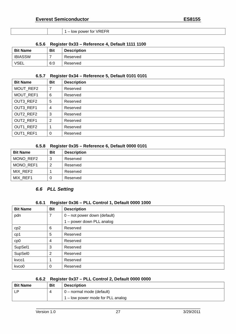
1 – low power for VREFR 6.5.6 Register 0x33 – Reference 4, Default 1111 1100
Bit Name Bit Description IBIASSW 7 Reserved VSEL 6:0 Reserved
6.5.7 Register 0x34 – Reference 5, Default 0101 0101
Bit Name Bit Description MOUT_REF2 7 Reserved MOUT_REF1 6 Reserved OUT3_REF2 5 Reserved OUT3_REF1 4 Reserved OUT2_REF2 3 Reserved OUT2_REF1 2 Reserved OUT1_REF2 1 Reserved OUT1_REF1 0 Reserved
6.5.8 Register 0x35 – Reference 6, Default 0000 0101
Bit Name Bit Description MONO_REF2 3 Reserved MONO_REF1 2 Reserved MIX_REF2 1 Reserved MIX_REF1 0 Reserved
6.6 PLL Setting 6.6.1 Register 0x36 – PLL Control 1, Default 0000 1000
Bit Name Bit Description pdn 7 0 – not power down (default)
1 – power down PLL analog cp2 6 Reserved cp1 5 Reserved cp0 4 Reserved SupSel1 3 Reserved SupSel0 2 Reserved kvco1 1 Reserved kvco0 0 Reserved
6.6.2 Register 0x37 – PLL Control 2, Default 0000 0000
Bit Name Bit Description LP 4 0 – normal mode (default)
1 – low power mode for PLL analog
Everest Semiconductor ES8155
Version 1.0 3/29/2011 28
MCLKSEL 3 Select internal master clock 0 – from MCLK pin (default) 1 – from PLL (to use PLL, make sure PLLEN=1, PLL_RB=1, otherwise, the setting will close chip clock)
PLLOUT_DIV2 2 0 – divide disabled, PLL out clock is vcoout/4 (default) 1 – divide enabled, PLL out clock is vcoout/8
PLL_RB 1 0 – PLL held in reset (default) 1 – PLL running (if PLLEN=1)
PLL_EN 0 0 – PLL disabled (default) 1 – PLL enabled
6.6.3 Register 0x38 – PLL Control 3, Default 0000 0000
Bit Name Bit Description DITH_MAG 6:4 Reserved PLL_N 3:0 Integer part of PLL input/output frequency ratio; Use value greater than 5 and less than 13
6.6.4 Register 0x39 – PLL_K[21:16], Default 0000 0000
Bit Name Bit Description PLL_K[21:16] 5:0 Fractional part of PLL input/output frequency ratio (treat as one 22-digital binary number)
6.6.5 Register 0x3A – PLL_K[15:8], Default 0000 0000
Bit Name Bit Description PLL_K[15:8] 7:0 Fractional part of PLL input/output frequency ratio (treat as one 22-digital binary number)
6.6.6 Register 0x3B – PLL_K[7:0], Default 0000 0000
Bit Name Bit Description PLL_K[7:0] 7:0 Fractional part of PLL input/output frequency ratio (treat as one 22-digital binary number)
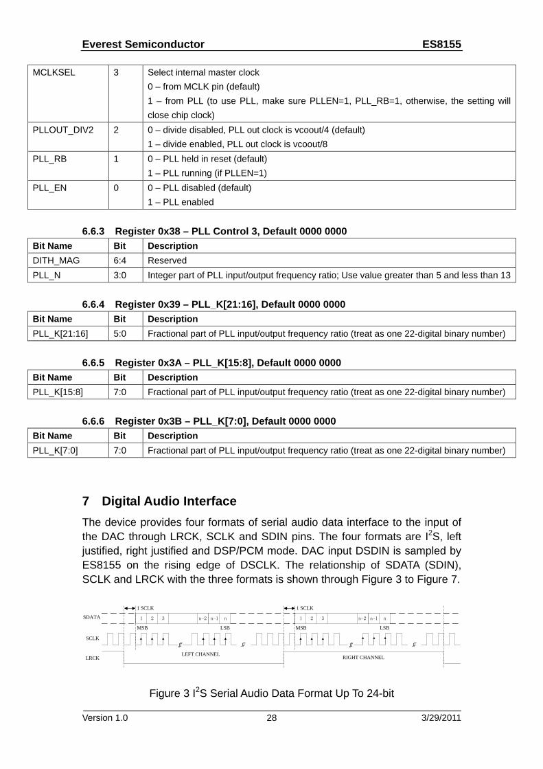
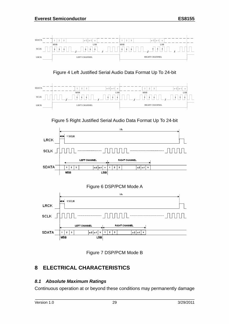
7 Digital Audio Interface The device provides four formats of serial audio data interface to the input of the DAC through LRCK, SCLK and SDIN pins. The four formats are I2S, left justified, right justified and DSP/PCM mode. DAC input DSDIN is sampled by ES8155 on the rising edge of DSCLK. The relationship of SDATA (SDIN), SCLK and LRCK with the three formats is shown through Figure 3 to Figure 7.
n-2 n-1 n321
1 SCLK
MSB LSB
LEFT CHANNEL
n-2 n-1 n321
1 SCLK
MSB LSB
RIGHT CHANNEL
SDATA
SCLK
LRCK
Figure 3 I2S Serial Audio Data Format Up To 24-bit
Everest Semiconductor ES8155
Version 1.0 3/29/2011 29
n-2 n-1 n321
MSB LSB
LEFT CHANNEL
n-2 n-1 n321
MSB LSB
RIGHT CHANNEL
SDATA
SCLK
LRCK
Figure 4 Left Justified Serial Audio Data Format Up To 24-bit
n-2 n-1 n321
MSB LSB
LEFT CHANNEL
n-2 n-1 n321
MSB LSB
RIGHT CHANNEL
SDATA
SCLK
LRCK
Figure 5 Right Justified Serial Audio Data Format Up To 24-bit
Figure 6 DSP/PCM Mode A
Figure 7 DSP/PCM Mode B
8 ELECTRICAL CHARACTERISTICS
8.1 Absolute Maximum Ratings Continuous operation at or beyond these conditions may permanently damage
Everest Semiconductor ES8155
Version 1.0 3/29/2011 30
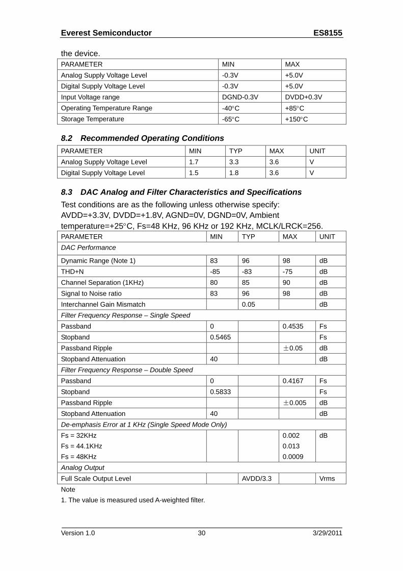
the device. PARAMETER MIN MAX Analog Supply Voltage Level -0.3V +5.0V Digital Supply Voltage Level -0.3V +5.0V Input Voltage range DGND-0.3V DVDD+0.3V Operating Temperature Range -40°C +85°C Storage Temperature -65°C +150°C
8.2 Recommended Operating Conditions PARAMETER MIN TYP MAX UNIT Analog Supply Voltage Level 1.7 3.3 3.6 V Digital Supply Voltage Level 1.5 1.8 3.6 V
8.3 DAC Analog and Filter Characteristics and Specifications Test conditions are as the following unless otherwise specify: AVDD=+3.3V, DVDD=+1.8V, AGND=0V, DGND=0V, Ambient temperature=+25°C, Fs=48 KHz, 96 KHz or 192 KHz, MCLK/LRCK=256. PARAMETER MIN TYP MAX UNIT DAC Performance
Dynamic Range (Note 1) 83 96 98 dB THD+N -85 -83 -75 dB Channel Separation (1KHz) 80 85 90 dB Signal to Noise ratio 83 96 98 dB Interchannel Gain Mismatch 0.05 dB Filter Frequency Response – Single Speed Passband 0 0.4535 Fs Stopband 0.5465 Fs Passband Ripple ±0.05 dB Stopband Attenuation 40 dB Filter Frequency Response – Double Speed Passband 0 0.4167 Fs Stopband 0.5833 Fs Passband Ripple ±0.005 dB Stopband Attenuation 40 dB De-emphasis Error at 1 KHz (Single Speed Mode Only) Fs = 32KHz Fs = 44.1KHz Fs = 48KHz
0.002 0.013 0.0009
dB
Analog Output Full Scale Output Level AVDD/3.3 Vrms Note 1. The value is measured used A-weighted filter.
Everest Semiconductor ES8155
Version 1.0 3/29/2011 31
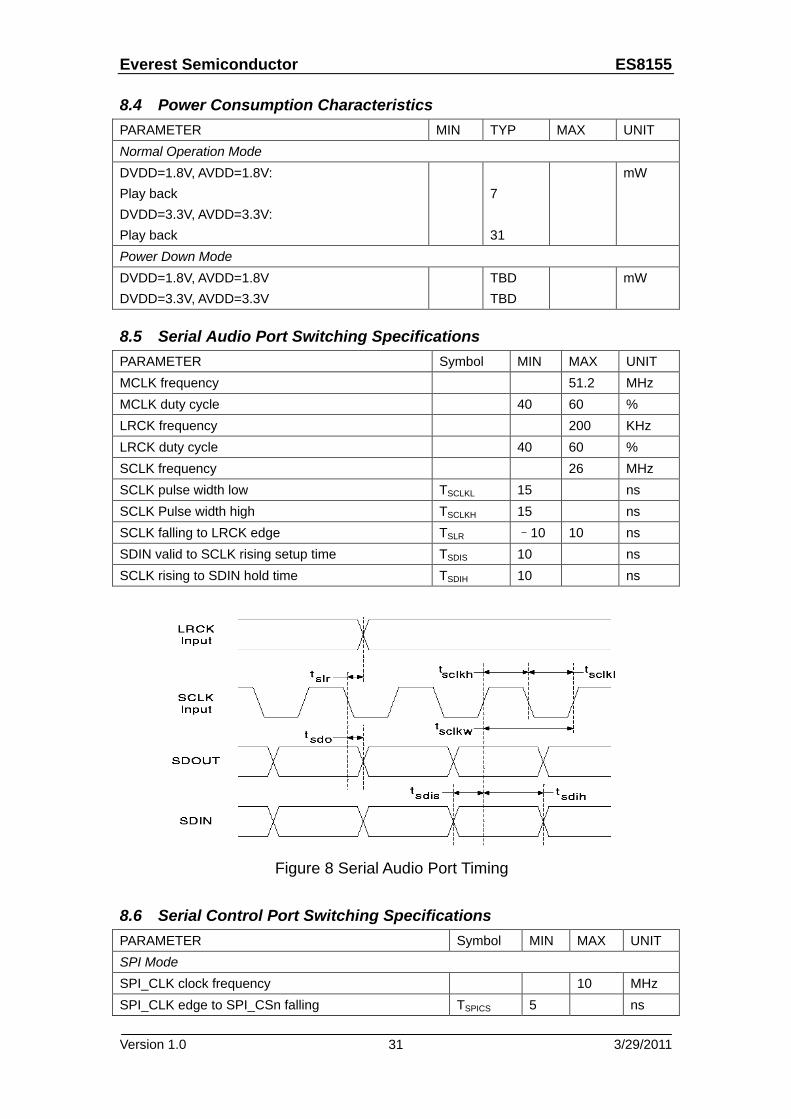
8.4 Power Consumption Characteristics PARAMETER MIN TYP MAX UNIT Normal Operation Mode DVDD=1.8V, AVDD=1.8V: Play back DVDD=3.3V, AVDD=3.3V: Play back
7 31
mW
Power Down Mode DVDD=1.8V, AVDD=1.8V DVDD=3.3V, AVDD=3.3V
TBD TBD
mW
8.5 Serial Audio Port Switching Specifications PARAMETER Symbol MIN MAX UNIT MCLK frequency 51.2 MHz MCLK duty cycle 40 60 % LRCK frequency 200 KHz LRCK duty cycle 40 60 % SCLK frequency 26 MHz SCLK pulse width low TSCLKL 15 ns SCLK Pulse width high TSCLKH 15 ns SCLK falling to LRCK edge TSLR –10 10 ns SDIN valid to SCLK rising setup time TSDIS 10 ns SCLK rising to SDIN hold time TSDIH 10 ns
8.6 Serial Control Port Switching Specifications PARAMETER Symbol MIN MAX UNIT SPI Mode SPI_CLK clock frequency 10 MHz SPI_CLK edge to SPI_CSn falling TSPICS 5 ns
Figure 8 Serial Audio Port Timing
Everest Semiconductor ES8155
Version 1.0 3/29/2011 32
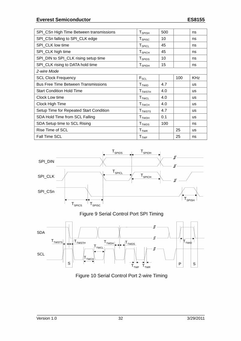
SPI_CSn High Time Between transmissions TSPISH 500 ns SPI_CSn falling to SPI_CLK edge TSPISC 10 ns SPI_CLK low time TSPICL 45 ns SPI_CLK high time TSPICH 45 ns SPI_DIN to SPI_CLK rising setup time TSPIDS 10 ns SPI_CLK rising to DATA hold time TSPIDH 15 ns 2-wire Mode SCL Clock Frequency FSCL 100 KHz Bus Free Time Between Transmissions TTWID 4.7 us Start Condition Hold Time TTWSTH 4.0 us Clock Low time TTWCL 4.0 us Clock High Time TTWCH 4.0 us Setup Time for Repeated Start Condition TTWSTS 4.7 us SDA Hold Time from SCL Falling TTWDH 0.1 us SDA Setup time to SCL Rising TTWDS 100 ns Rise Time of SCL TTWR 25 us Fall Time SCL TTWF 25 ns
SPI_DIN
SPI_CLK
SPI_CSn
TSPICS TSPISC
TSPIDS TSPIDH
TSPICH
TSPICL
TSPISH
S P
SDA
SCL
TTWSTS TTWSTH
TTWCH
TTWCL
TTWDH TTWDS
TTWF TTWRS
TTWID
Figure 10 Serial Control Port 2-wire Timing
Figure 9 Serial Control Port SPI Timing
Everest Semiconductor ES8155
Version 1.0 3/29/2011 33
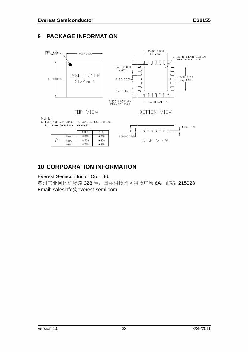
9 PACKAGE INFORMATION
10 CORPOARATION INFORMATION Everest Semiconductor Co., Ltd. 苏州工业园区机场路 328 号,国际科技园区科技广场 6A,邮编 215028 Email: [email protected]