Embed Size (px)
Citation preview
Advanced AFM/SPMProducts & Solutions for Industry and Research
XE-70™ Product DatasheetGeneral Purpose AFM/SPM for Nano Science
From a compact mechanical design standpoint, the XE‑70 satisfies an economic extension of the XE‑100 and continues the innovative technology of the XE‑Series AFM (Atomic Force Microscope). Utilizing the same modes, options, and electronics of the XE‑100 and the rest of the XE‑Series AFMs, the XE‑70 matches the former XE‑Series in performance and flexibility. Especially minimized form factor of the XE‑70 also outperforms in True Non‑Contact Mode optimally, which is the ultimate AFM/SPM (Scanning Probe Microscope) solution for non‑contact nanoscale metrology and characterization of small samples in data storage, semiconductors, nanoscience, materials science, polymers, and electrochemistry. The versatile platform of the XE‑70 has been meticulously designed to meet the diverse functional needs of today’s AFM/SPM users.
General Purpose AFM with True Non-Contact and Full SPM Mode Support
Since the invention of AFM, this technology enables researchers to understand the surface morphology of materials at the nanoscale along with various physical properties in a non‑destructive manner. In the early stages of AFM studies, the main research goal was to invent and develop AFM and additional modes such as MFM (Magnetic Force Microscopy), SCM (Scanning Capacitance Microscopy), and SThM (Scanning Thermal Microscopy). As the modes of the AFM became more established, its role has shifted from the study goal itself to a tool which may provide preliminary physical data of samples at the nanoscale. Therefore it was rapidly introduced to other research fields including semiconductor research, material science, and even biological applications. To provide appropriate measurements of physical and electrical properties of samples, AFM should be outperforming in metrology, and is also functional in additional SPM modes.Among its capabilities, precise metrological measurement
is important which not only means the main performance of AFM, but the ability to rule out topographical artifacts mixed in with other physical properties. That includes precise control of tip‑sample distance and tip wear‑out, which is optimized in True Non‑Contact Mode. When non‑contact AFM (NC‑AFM) is operated with a very small tip‑sample distance, even a slight deviation of tip‑sample interaction force from the set point can be detrimental, unlike in the contact mode. This is why the tip has to be significantly far from the sample surface in conventional NC‑AFM, resulting in poor resolution. It is a
technically challenging task to implement NC‑AFM mode with a very small tip‑sample distance. Tapping mode was initially used to avoid the limitation of precise tip‑sample spacing control. Once correctly engineered, however, True Non‑Contact Mode provides the ultimate resolution of ambient AFM, far surpassing the capabilities of both Contact and Tapping mode. (See appendix for details on “True Non‑Contact Mode vs. Tapping Mode”)Introduced by the original innovators and pioneers of AFM
technology after 4 years of intensive research and product development, the XE Series represents breakthroughs in every aspect of AFM/SPM technology. The XE Series is the first and only AFM/SPM in the market that realizes True Non‑Contact Mode in every specification, not just in principle but in practice. True Non‑Contact Mode achieves an unprecedented tip‑sample distance, combined with superb tip and sample surface preservation. The advantages of True Non‑Contact Mode enable the ultimate resolution of AFM and measurement accuracy which are without peer in the AFM/SPM industry. (See appendix for details on “What is the ultimate resolution of AFM?”)
XE-70, for general purpose AFM/SPM measurements

- � -
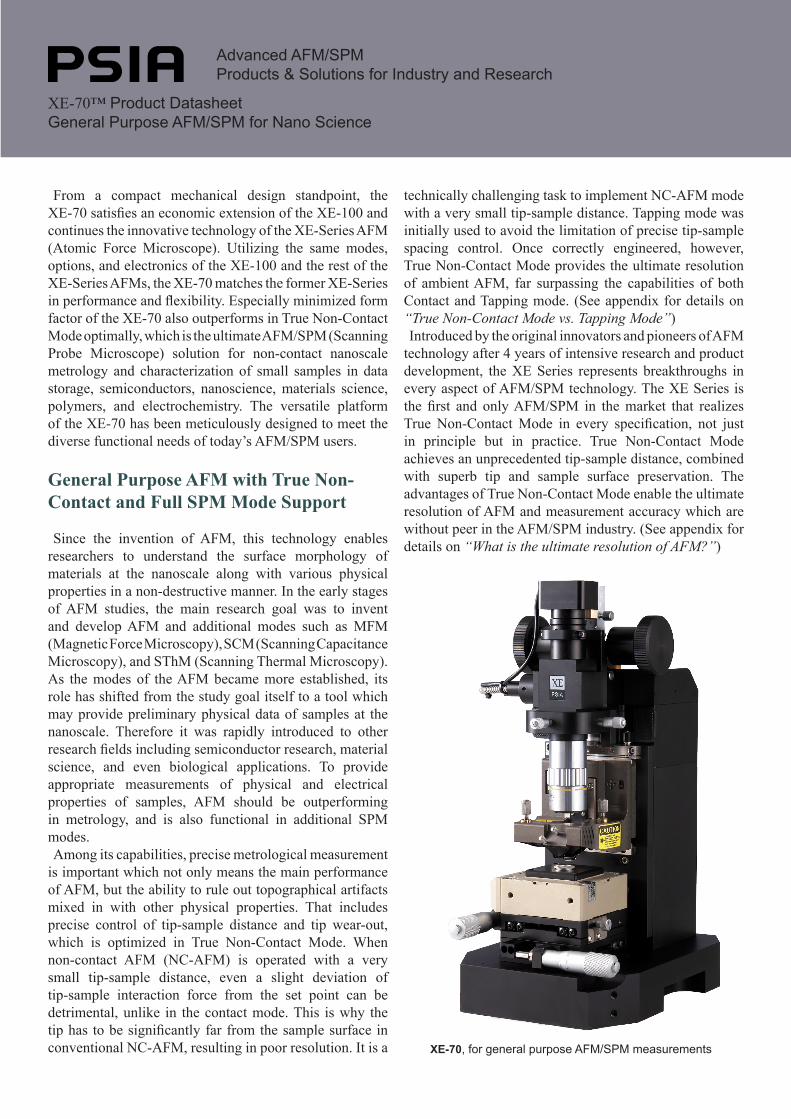
XE Scanning Mechanism
The XE scan system is a core feature that gives the competitive edge to the XE‑Series over other, more traditional designed AFM/SPMs. PSIA’s innovative scanner design separates the Z scanner from the XY, enabling exceptional Z‑servo performance, orthogonality, and scan accuracy, unmatched by other AFM/SPMs. Both the XY and Z scanner are designed to have great versatility.
Separation of XY & Z ScannerThe Z scanner, which controls the vertical movement of
the AFM tip and is fundamental to acquiring the surface morphology information, is completely decoupled from the XY scanner which moves sample in X and Y horizontal directions. This architectural change provides the user with significant operational advantages enabling True Non‑Contact Mode.
Physical separation of the XY scanner from the Z scanner completely removes background curvature from a fundamental standpoint, and effectively eliminates the cross‑talk and non‑linearity problems that are intrinsic to conventional piezoelectric tube based AFM systems. This uniquely designed XE scan system not only increases the data collecting speed by at least 10 times compared to a conventional tube type scanner, but also minimizes the error due to the inherent non‑linearity of the scanner itself.
High Performance Z-ServoThe Z scanner, being separate from the XY scanner,
is designed to have a higher resonant frequency than conventional piezoelectric tube scanners. For this reason, a stacked piezo actuator is used for the Z scanner, which has a very fast response speed, at least 10 kHz, with a high push‑pull force when appropriately pre‑loaded. Since the
XE Scanning MechanismDecoupled XY and Z ScannerUltra High Speed Z Scanner2D Flexure Guided XY ScannerHardware Closed-loop Feedback
XE Electronics21 channels of 16-bit DACs20 channels of 16-bit ADCsSimultaneous acquisition of 16 data imagesI/O of AFM signals via Signal Access Module16.7 Mega pixel data (up to 4096 × 4096)
XE SoftwareXEP – Data Acquisition SoftwareXEI – Data Analysis, Image Processing and Intuitive ReportingXEC – Vision System for AFM OperationXER – Remote Access Protocol for XE-AFMAuxiliary Softwares
for Lithography and Automated Imaging
User ConvenienceSLD XE Head – No Interference NoiseDirect On-Axis OpticsOptical Measurement SupportProbe ExchangeAcoustic EnclosureXE Optical Head for Optical ExperimentsClip-type Probehand25 µm Z scanner
Full Support of AFM/SPM ModesTrue Non-Contact ModeContact ModeDynamic Force MicroscopyPhase ImagingF-d Spectroscopy
Current-AFM and I-V SpectroscopyElectric Force Microscopy / DC-EFM Force Modulation Microscopy Magnetic Force MicroscopyScanning Capacitance MicroscopyScanning Spreading Resistance MicroscopyScanning Tunneling MicroscopyScanning Thermal MicroscopyNano-indentation / Scratch NanolithographyNanomanipulation
True Non-Contact AFM image of a polymer sphere (6 × 6 µm). It is not possible to image this sphere in tapping or contact mode. Only True Non-Contact Mode from the XE-Series with high z-servo performance can accurately image the steep variations of such soft materials.
- � -
Z‑servo response of the XE scan system is very accurate, the probe can precisely follow the steep curvature of a sample without crashing or sticking to the surface. This enables more than 10 times faster scan rates than achievable with a conventional tube type scanner, increasing the speed of the measurements, and enhancing the tip lifetime, resulting in the ability to acquire clear images for an extended period of time. A very high performance Z‑servo system is required for True Non‑Contact Mode. The mechanical response of the Z scanner has to be extremely fast, a requirement met only by the XE scan system.
2D Flexure XY ScannerIn the XE scan system, the XY scanner is a Body Guided
Flexure scanner, which is used to scan a sample in the X and Y directions only. The flexure hinge structure of the XY scanner guarantees highly orthogonal 2D movement with minimum out‑of‑plane motion. The 2D flexure stage of the XE scan system has only 1‑2 nm of out‑of‑plane motion for the scan range of 50 µm, compared to the inherent 80 nm by the tube scanner of conventional AFMs over the same scan range. Due to the Parallel Kinematics design, the X‑Y scanner also has low inertia and axis‑independent performance.
The symmetrical flexure scanner design also makes possible to place much larger samples on the sample stage than could normally be accommodated by a piezoelectric tube type scanner. Because the symmetrical structure of the X‑Y scanner keeps the scanner balanced even when a sample is loaded, the dynamics of the X‑Y scanner is not distorted by the sample holder and/or the loaded sample. Furthermore, since the flexure scanner only moves in the X‑Y direction it can be scanned at much higher rates (10~50 Hz) than would be possible with a standard AFM.
XE Electronics
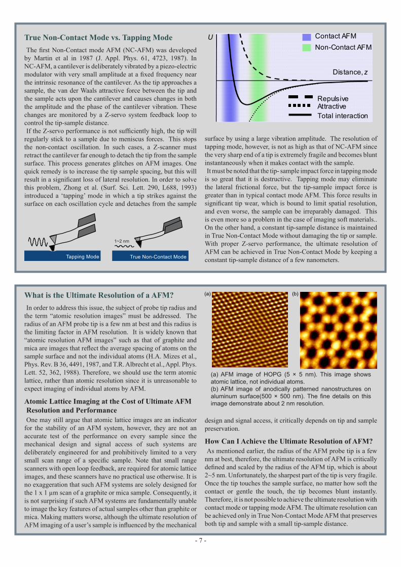
High Speed MeasurementThe XE‑Series not only achieves a structural design
innovation that yields a trend setting AFM performance, but it also brings state‑of‑the‑art improvements to the electronics. The XE Control Electronics incorporates advanced digital circuitry with precision software and hardware components that empower high speed and high capacity data processing. It has a fast and powerful DSP (Digital Signal Processor), 21 channels of 16‑bit DACs (Digital to Analog Converters), and 20 channels of 16‑bit ADCs (Analog to Digital Converters). The XE Control Electronics are designed to enable the scanner, the core unit of the AFM, to provide efficient, accurate and fast control, and to facilitate the acquisition of a stable image even beyond a scan speed of 10Hz.
XE Scan System moves the Z scanner orthogonally decoupled from the X-Y, enabling exceptional Z-servo performance and scan accuracy. The innovative optical design allows for direct on-axis optical view of a sample from the top, the first and only AFM/SPM system in the industry.
Cantilever Deflection Measurement Scheme of the XE-Series. The cantilever and the PSPD moves simultaneously and in parallel, while the Z scanner is on the feedback.
NC-AFM image of 0.16 μm wide, 0.55 μm deep trenches shown in 1:1 aspect ratio 3D rendering (1.5 × 1.5 μm). It is not possible to image such narrow and deep trenches in conventional AFMs. Only True Non-Contact Mode from the XE-Series with high Z-servo performance can accurately trace the steep walls of the trenches.

‑ 4 ‑
Simultaneous Multiple Data Processing with up to 16.7 Mega pixelsXE’s powerful electronics enables multiple data channels,
being able to simultaneously record up to 16 data channels per measurement, and the size of each data image can be up to 16.7 Mega pixels. User can adjust the size of the data image freely, and analyze and compare multiple data sets on the same screen of the image processing/analysis software, XEI.
Closed-loop Scan SystemBesides the high speed measurement ability, XE’s
electronics controls the movement of the AFM system precisely by the closed‑loop scan system, which is indispensable to map each additional property to the very point of enhanced topographic details. Even though an AFM system can acquire data with multiple modes, unless the system displays the exact position of measurement, it needs software correction (or calibration) to map the data on the exact position. Correction by software remapping usually works well when the imaging area is comparatively small, but closed‑loop scan is applicable on any imaging area without distortion.
Signal Access Module In addition, the controller contains input/output
terminals that provide a simple means for users to design advanced experiments that extend far beyond the tool’s basic capabilities and are much more complicated than obtaining basic images. It is the most advanced AFM/SPM controller with superb features, functionality, flexibility, and expandability.
PeripheralsFurthermore, the operating computer is equipped with
the latest high power Intel® Pentium™ 4 processor and Microsoft® Windows® XP operating system. A 19” LCD monitors displays crystal clear images using DVI (Digital Video Interface). All necessary software packages, including XEP, the Data Acquisition program, and XEI, the Image Processing program, are installed on the computer. XE Software
XEP is a data acquisition program that communicates with the XE Control Electronics in order to control the XE‑Series system. The XEP interface allows a user to investigate and analyze a sample area. that is, XEP controls and operates the XE system to collect sample data. XEP supports all the standard and advanced measurement modes.
XEP has full windows multi‑tasking capability with Windows XP based data acquisition and imaging processing programs. It can acquire up to 16 images simultaneously in both forward and reverse scan with real time auto‑tilt and auto‑contrast. XEP provides arbitrary data pixel size in both X and Y directions, up to 4096 × 4096. All images are originally in TIFF format, and can be exported as PNG, JPEG and Text files.
2D guided flexure scanner of the XE-70 enables distortionless high-resolution imaging without background curvature. The raw surface topography images of a bare silicon wafer are compared between conventional tube scanner (a), and the 2D flexure stage (b).
XEP, the AFM control software for XE-70, supports all the modes of AFM. It can acquire up to 16 channels of data simultaneously.
XEI processes and analyzes AFM image data. XEI is designed for generating intuitive and streamlined reports for researchers.

‑ 5 ‑
XEI is an excellent software package that provides user‑friendly and dynamic tools for image processing, quantitative analysis and statistics, including exporting and printing of processed images and measurement results. It is quite important to make good use of the XEI image processing program, just as it is important to collect the best possible data utilizing the XEP data acquisition program. The XEI software maximizes the system’s potential by allowing users to extract more information from the sample surface by utilizing various analysis tools and also by providing the ability to remove certain accidental artifacts from the scan data.
XEI supports all the standard imaging processing such as Fourier Power Spectrum editor, low pass filter and deglitch, and 1st, 2nd, and 3rd order polynomial surface fit. Its analysis functions include but are not limited to user selectable Profile Tracer and Region, Line Measurement of Height, Line Profile, Line Histogram, Region Measurement of Height, Average Roughness, Surface Area, Histogram, Grain Analysis Functions, and many more. If the customer requires additional, non standard XEI functionality, PSIA will gladly accommodate such customer’s demand. For presentations purposes, users can take advantage of our powerful 3‑D image rendering and multi‑image presentation with user selectable color palette. Furthermore, XEI is based on Java™ platform, which enables XEI running on any operating system including Microsoft® Windows® XP, Windows NT®, Mac OS® X, Linux, etc.
User ConvenienceSLD XE AFM HeadXE‑70 uses SLD (Super Luminesence Diode) for cantilever
deflection detection. To avoid interference noise from coherent conventional red laser diode, SLD is introduced to prevent any noise interference, which is crucial in low force F‑d spectroscopy and precision topography measurement. It also is introduced in consideration of optical set‑up, which does not infringe on the region of visual light.
Direct On-Axis OpticsAn optical microscope (with magnification of 10x) is used
to focus the laser beam onto the cantilever and to locate the regions of interest on the sample surface that is to be measured. Since there is suitable clearance above the XE scan head, it is possible to accommodate a direct on‑axis optical microscope. The direct on‑axis optics is the first in the industry that revolutionizes the way AFM users view their samples by providing the natural, on‑axis views with unprecedented clarity.
Clear On-Axis Arrangement of Optical ComponentsA crucial point of the XE‑series design is to ensure that
the laser beam falls on the same point on the cantilever and the reflected beam hits the same point on the Photo Sensitive Photo Detector (PSPD) regardless of the Z scanner motion, so that only the deflection of the cantilever will be monitored by the PSPD. Moreover, the laser beam path configuration is optimized so as not to interfere with a clear on‑axis optical view of the scanning probe and sample surface. In the XE system, since the laser beam is directed to the cantilever from a vertical direction, the beam always
XE-70’s optical vision delivers users clear view of sample surface and cantilever position. The purple spot on the cantilever is the SLD beam spot which is undetected by human eyes.
Probe tip exchange is just a snap with our patented pre-aligned kinematic chip mount
The XE head can be easily removed by turning the dovetail lock and sliding the head from the dovetail rail.

‑ 6 ‑
hits the same point on the cantilever regardless of the Z scanner motion. Therefore, once the laser beam is aligned, there is no need to realign the laser beam, even after the Z scanner has engaged with samples. Also the objective lens, tube lens, and digital CMOS camera are rigidly mounted on a single body and move together for panning and focusing to preserve the highest quality optical vision.
Optical Measurement SupportDue to the optical consideration of XE‑AFM, XE‑Series
provides XE Optical Head (optional) to support various optical instruments including Raman spectroscopy. The structure of the XE Optical Head provides a wide optical path for external optical instruments, which are not easy to achieve in other commercial AFMs.In addition, the XE Optical Head is provided with SLD
(center wavelength of 830 nm) for cantilever deflection detection, which is adopted to avoid interruption when optics of the visible ray region are used in an experiment.
Laser Beam AlignmentSince the digital CMOS camera is aligned directly with
the cantilever with nothing blocking its optical view, it is very convenient to focus on or to observe the sample while moving the camera up and down. To align the laser beam, conventional AFMs use additional positioning equipment, the operation of which is often difficult and cumbersome. However, laser beam alignment becomes easy and convenient with the XE‑Series. Manageable control knobs on the XE‑Series head can be adjusted manually with the help of the control software, making the location and movement of the laser beam easy and accurate.
Probe Tip ExchangeAlthough greatly enhanced tip lifetimes are achieved, it is
necessary to replace the tip probe after certain amount of usage. Probe tip exchange is just a snap with our patented pre-aligned kinematic chip mount that guarantees the same position of a probe tip every time you need to exchange a cantilever. The magnetically coupled kinematic chip mount allows you to exchange a probe tip without the need of tools or head removal.A clip‑type probehand also can be provided for user flexibity, which supports any conventional unmounted cantilevers to be utilized directly.
Dovetail Lock Head MountWith our patented dovetail lock head mount, the AFM
head removal is no longer an expert operation. The AFM head, which includes the Z scanner, is easily inserted or removed by sliding it along a dovetail rail and locking it into place with a convenient turn of two thumb locks. There are no additional knobs or springs to adjust as is common with other AFM designs.
Acoustic Enclosure (Optional)The XE‑70 can be supplied with a hermetically sealed
acoustic enclosure that shows trend‑setting high efficiency in blocking external optical and acoustic noise.
Supporting AFM/SPM Modes
The XE‑70 supports all the modes which are available with the XE‑Series AFMs. The strength of XE‑70 comes from sharing all these options and modes with other XE‑Series AFMs, with proven track records in the scientific community.
True Non-Contact Mode enables acquiring the topographical data without modifying the surface of sample. Due to the decoupled XY and Z scanning structure, XE‑AFM scans the sample surface with high precision resolution.
Phase Imaging is another technique that can be used to map variations in surface properties such as elasticity, adhesion, and friction. It can be produced while an XE‑Series AFM is operating in True Non‑Contact, EFM, or MFM mode.
F-d Spectroscopy is used to measure the vertical force that the tip applies to the surface while a contact‑AFM image is being taken. This technique can also be used to analyze surface contaminants, viscosity, lubrication thickness, and local variations in the elastic properties of the surface.
Current-AFM and I-V Spectroscopy measures the sample conductance/resistance by detecting the electric current up to pico‑ampere from sample surface. For example, the leakage current of sample can be measured by Current‑AFM.
Electric Force Microscopy of XE‑Series AFM maps electric properties of a sample surface by measuring the electrostatic force between the surface and a biased cantilever. By direct observation, sample information such as the surface potential and charge distribution can be found.
Magnetic Force Microscopy measures magnetic properties of samples by reading the magnetic force between the magnetized tip and sample. By utilizing True Non‑Contact Mode, XE‑70 effectively eliminates topographical influence from magnetic fields.
Scanning Capacitance Microscopy is the key to visualize the electronic structure of semiconductors. By measuring the capacitance variation, SCM displays the doping rate of semiconductors.
Scanning Thermal Microscopy probes thermal properties at the nanoscale using nanofabricated thermal probes. The XE‑Series AFMs achieved nanometer scale resolution which is not achievable if a traditional Wollaston wire is used as a probe.
Intel is a registered trademark of Intel Corporation.Microsoft, Windows, and Windows NT are registered trademarks of
Microsoft Corporation.Mac OS is a registered trademark of Apple Computer, Inc.
Pentium is a trademark of Intel Corporation.Java is a trademark of Sun Microsystems, Inc.
- 7 -
True Non-Contact Mode vs. Tapping ModeThe first Non‑Contact mode AFM (NC‑AFM) was developed
by Martin et al in 1987 (J. Appl. Phys. 61, 4723, 1987). In NC‑AFM, a cantilever is deliberately vibrated by a piezo‑electric modulator with very small amplitude at a fixed frequency near the intrinsic resonance of the cantilever. As the tip approaches a sample, the van der Waals attractive force between the tip and the sample acts upon the cantilever and causes changes in both the amplitude and the phase of the cantilever vibration. These changes are monitored by a Z‑servo system feedback loop to control the tip‑sample distance. If the Z‑servo performance is not sufficiently high, the tip will
regularly stick to a sample due to meniscus forces. This stops the non‑contact oscillation. In such cases, a Z‑scanner must retract the cantilever far enough to detach the tip from the sample surface. This process generates glitches on AFM images. One quick remedy is to increase the tip sample spacing, but this will result in a significant loss of lateral resolution. In order to solve this problem, Zhong et al. (Surf. Sci. Lett. 290, L688, 1993) introduced a ‘tapping’ mode in which a tip strikes against the surface on each oscillation cycle and detaches from the sample
surface by using a large vibration amplitude. The resolution of tapping mode, however, is not as high as that of NC‑AFM since the very sharp end of a tip is extremely fragile and becomes blunt instantaneously when it makes contact with the sample. It must be noted that the tip‑ sample impact force in tapping mode
is so great that it is destructive. Tapping mode may eliminate the lateral frictional force, but the tip‑sample impact force is greater than in typical contact mode AFM. This force results in significant tip wear, which is bound to limit spatial resolution, and even worse, the sample can be irreparably damaged. This is even more so a problem in the case of imaging soft materials.. On the other hand, a constant tip‑sample distance is maintained in True Non‑Contact Mode without damaging the tip or sample. With proper Z‑servo performance, the ultimate resolution of AFM can be achieved in True Non‑Contact Mode by keeping a constant tip‑sample distance of a few nanometers.
What is the Ultimate Resolution of a AFM? In order to address this issue, the subject of probe tip radius and
the term “atomic resolution images” must be addressed. The radius of an AFM probe tip is a few nm at best and this radius is the limiting factor in AFM resolution. It is widely known that “atomic resolution AFM images” such as that of graphite and mica are images that reflect the average spacing of atoms on the sample surface and not the individual atoms (H.A. Mizes et al., Phys. Rev. B 36, 4491, 1987, and T.R. Albrecht et al., Appl. Phys. Lett. 52, 362, 1988). Therefore, we should use the term atomic lattice, rather than atomic resolution since it is unreasonable to expect imaging of individual atoms by AFM.
Atomic Lattice Imaging at the Cost of Ultimate AFM Resolution and PerformanceOne may still argue that atomic lattice images are an indicator
for the stability of an AFM system, however, they are not an accurate test of the performance on every sample since the mechanical design and signal access of such systems are deliberately engineered for and prohibitively limited to a very small scan range of a specific sample. Note that small range scanners with open loop feedback, are required for atomic lattice images, and these scanners have no practical use otherwise. It is no exaggeration that such AFM systems are solely designed for the 1 x 1 µm scan of a graphite or mica sample. Consequently, it is not surprising if such AFM systems are fundamentally unable to image the key features of actual samples other than graphite or mica. Making matters worse, although the ultimate resolution of AFM imaging of a user’s sample is influenced by the mechanical
design and signal access, it critically depends on tip and sample preservation.
How Can I Achieve the Ultimate Resolution of AFM?As mentioned earlier, the radius of the AFM probe tip is a few
nm at best, therefore, the ultimate resolution of AFM is critically defined and scaled by the radius of the AFM tip, which is about 2~5 nm. Unfortunately, the sharpest part of the tip is very fragile. Once the tip touches the sample surface, no matter how soft the contact or gentle the touch, the tip becomes blunt instantly. Therefore, it is not possible to achieve the ultimate resolution with contact mode or tapping mode AFM. The ultimate resolution can be achieved only in True Non‑Contact Mode AFM that preserves both tip and sample with a small tip‑sample distance.
(a) AFM image of HOPG (5 × 5 nm). This image shows atomic lattice, not individual atoms. (b) AFM image of anodically patterned nanostructures on aluminum surface(500 × 500 nm). The fine details on this image demonstrate about 2 nm resolution.
True Non-Contact ModeTapping Mode
1~2 nm

PSIA Inc.3040 Olcott St.Santa Clara, CA 95054Toll Free +1-866-979-9330Phone +1-408-986-1110Fax +1-408-986-1199
PSIA Corp.KANC 4FIui-Dong 906-10Suwon, Korea 443-766Phone +82-31-546-6800Fax +82-31546-6805
Website: http://www.psiainc.come-mail: [email protected]
Rev. 11-14-06
SPECIFICATIONSMechanical
Sample Size: Up to 100 × 100 mm, up to 20 mm thickSample Mass: Up to 500 gSample Stage: 25 × 25 mm with manual micrometer, 10 μm per notch
XY ScannerScanner Type: Single module parallel‑kinematics flexure stage with closed loop feedback Scan size: 5 × 5 μm 50 × 50 μm (5 × 5 μm in low voltage mode) 100 × 100 μm (10 × 10 μm in low voltage mode)Resolution: < 0.15 nm (< 0.02 nm in low voltage mode)
Z ScannerScanner Type: Guided flexure stage with closed loop feedbackScan size: 12 μm (1.7 μm in low voltage mode)Resolution: < 0.03 nm (< 0.01 nm in low voltage mode)
Z StageTravel: 30 mm travelResolution: 80 nmMax speed: 30,000 step/sec
OpticalMagnification: 800 ×Resolution: 1 μm (0.28 N.A.)Effective Picture Elements: XGA 1024 × 768 progressive CMOSDigital Interface: USB on a 19” LCD monitorFrame Rate: Up to 30 fpsField of View: 480 μm × 360 μm
ElectricalX, Y, Z Control Electronics: Closed‑loop hardware feedback scan position control systems in all 3 axesDSP control: 200 MHz CPU, 1000 MFLOPS DSPD/As: 21 channel 16‑bit DAC at 500 kHz settling,A/Ds: 20 channel 16‑bit ADC at 500 kHz samplingComputer‑to‑Controller Communication: USB
Computer§
Computer: Intel® Pentium™ 4 3.x GHz 1 GB RAM, 160 GB HD 19” LCD monitor CD‑RW/DVD‑ROMOperating System: Microsoft® Windows® XPGraphics: Super VGA graphics, 1280 × 1024 pixel
SoftwareXEP and XEI for data acquisition and image processing respectively
Operating EnvironmentTemperature: 5°C to 40°CHumidity: 30% ~ 80%, non‑condensingVibration: Vertical floor vibration less than 1×10‑8 m/sec for 0‑50 Hz
§ The specification of the computer provided can be changed to meet the best configuration to run a XE‑70 AFM system.
PSIA Inc.3040 Olcott St.Santa Clara, CA 95054Toll Free +1-866-979-9330Phone +1-408-986-1110Fax +1-408-986-1199
PSIA Corp.KANC 4FIui-Dong 906-10Suwon, Korea 443-766Phone +82-31-546-6800Fax +82-31-546-6805
Website: http://www.psiainc.come-mail: [email protected]
Rev. 2-07-07