Embed Size (px)
Citation preview
-AiS9 goo OPTICAL STUDY OF GER NIUN GERMANIUM PLUS ARSENIC AND t/2GERMANIUM PLUS GALL (U) AIR FORCE INST OF TECHWRIGHT-PATTERSON AF8 OH SCHOOL OF ENGI T G ALLEY
UNCLASSIFIED DEC 87 AFIT/GEP/ENP/87D-i F/G 20112 NI.
mENhECLhEmhhhEmohEEEmhhIEohEEEmhhhhmhE
120
1a .~r 8~
,OPOCOPY j 132UIO ET HR
fJI FILE CMP
~OF
OPTICAL STUDY OF GERMANIUM, GERMANIUMPLUS ARSENIC, AND GERMANIUM PLUS
GALLIUM IMPLANTS IN GALLIUM ARSENIDE
- THESIS
Thomas G. AlleyFirst Lieutenant, USAF
AFIT/GEP/ENP/87D-1
DTICQEL T Ef
DEPARTMENT OF THE AIRFORCE Q IDAIR UNIVERSITY _E
AIR FORCE INSTITUTE OF TECHNOLOGY
WrgtPtesnAr raRce Ohio
S88801 '04
AFI T/GEP/ENP/87D-1
0
e
OPTICAL STUDY OF GERMANIUM, GERMANIUMPLUS ARSENIC, AND GERMANIUM PLUS
GALLIUM IMPLANTS IN GALLIUM ARSENIDE
THES IS
Thomas G. AlleyFirst Lieutenant, USAF
AFIT/GEP/ENP/87D-1
ELECTE t\~.t'us0 31~988f~
Approved for public release; distribution unlimited
0
0
AFIT/GEP/ENP/87D-1
OPTICAL STUDY OF GERMANIUM,
GERMANIUM PLUS ARSENIC, AND GERMANIUM PLUS GALLIUM
IMPLANTS IN GALLIUM ARSENIDE
THESIS
Presented to the Faculty of the School of Engineering
of the Air Force Institue of Technology
Air University
In Partial Fulfillment of the art
Requirements for the Degree of
Master of Science in Engineering Physics
Accession For
~DTIC TABUnannounced []
Thomas G. Alley, B.A. B
First Lieutenant, USAF Distribution/~Availabilit Cods
I Avaii and/or -
December 19871& L
C Approved for public release; distribution unlimited
C.M
Table of Contents
Acknowledgements .................................. iii
Abstract .......................................... iv
List of Figures ................................... vi
List of Tables ................................... ix
I. Introduction ................................. 1
A. Gallium Arsenide ........................ 1B. Germanium Implanted Gallium Arsenide ..... 3C. Objective and Scope ...................... 4
II. Theory ....................................... 6
A. Intrinsic Semiconductor Energy States .... 6B. Extrinsic Semiconductors ................. 7C. Amphoteric Behavior ...................... 9D. Other Impurities and Defects ............. 10E. Ion Implantation ......................... 11F. Dual Implantation .................... 13G. Photoluminescence ..................... 13
* H. Radiative Transitions .................... 161. Band-to-Band Recombination ........... 182. Excitons ............................ 18
a. Free Exciton Transitions ......... 19b. Bound Exciton Transitions ........ 19
3. Free-to-Bound Transitions ............ 20• 4. Donor-Acceptor Pair Transitions ...... 20
5. Phonon Assisted Transitions .......... 22
III. Previous Work ................................ 23
A. Photoluminescence ....................... 23C B. Electrical Measurements .................. 24
IV. Description Of Experiment .................... 27
A. Sample Preparation ....................... 27B. Photoluminescence Experimental Setup ..... 29
1. Excitation Source and Setup .......... 292. Optical Detection System ............. 313. Sample Cryogenics .................... 34
V. Results and Discussion ....................... 38
C A. Control Substrate ........................ 38B. Main Indicators of Activity .............. 41
C
C. Ge Implanted GaAs ..................... .. .. . .. .. 421. Peaks Observed ...... . ... .. . ... .. .. . .. 422. Dose & Anneal Temperature Dependence. 45
D. Ge+As Implanted GaAs........................ 56E . Ge+Ga Implanted GaAs .............. 7F. Ion Species Comparison.................... 8
VI. Conclusions and Recommendations .............. 88
A. Conclusions.................................. 88*B. Recommendations ........................... 89
Bibliography.................................................. 91
Vita .............................................. .. 94
4C
C
Acknowledaements
I am very grateful for the help of all those that
provided assistance in tackling this thesis project. I'd
like to thank my advisors, Dr. R. L. Hengehold and Dr. Y. K.
Yeo for their advice and guidance. Many thanks go to Kevin
Keefer for his constant interest in this project and for the
amount of time he spent in helium transfers and guiding me
through the experimental setup. Additional thanks go to
Walt, Bill and Rick for their technical assistance.
Finally, I want to express my deepest gratitude to my
wife Valerie for her patience and support when our time
together was complicated by school, thesis, and a new son.
Thomas G. Alley
S
iii
C
AFIT/GEP/ENP/87D-1
he low t mpera - re photolumi 5 scence (PL propertie of
single implants and dual /.lants of je Geqio + oL r
into semi-insulatint! -dopedA__ have been analyzed. Room
temperature implantation was performed at 120 keV. When dual
implantation was used, samples were implanted at the, same .. -_-
dose and energy. Ion doses rMdmi to lx0/2.
Samples were encapsulated with andthen annealed at
temperatures ranging from 700 to 950Pc. SiNi was removed
cprior to PL measurements.A PL peak due to Ge-acceptors was identified. A bound
exciton peak related to Ge-donors wos_ also observed. An
*acceptor peak due to residual-J~was found in all samples.
The heights of the Ge-acceptor peak and exciton peak were
compared to the height of the intrinsic Si-acceptor peak.
The height comparison was used in an effort to find trends of
Ge-acceptor and Ge-donor transitions as a function of anneal
temperature and Ion dose. _.Z"Z'
The PL data for GaAs:Ge+As showed a relative decrease of
the Ge-acceptor related peak and an increase in the exciton
peak with increasing dose. This is generally consistent with
electrical measurements in previous work.
The PL data for GaAs:Ge at an anneal temperature of
9500C also showed a relative decrease in the Ge-acceptor
*related peak and an increase in the exciton peak with
iv
increasing dose. This is also consistent with electrical
data. However, trends of dose dependence at other anneal
temperatures were more complicated.
The anneal temperature dependence of the Ge related
peaks for both GaAs:Ge and GaAs:Ge+As showed complicated
behavior. At an anneal temperature of 800oC, the Ge-acceptor
related peak becomes obscured in a large Si-acceptor related
peak.
For GaAs:Ge+Ga, the addition of Ga to the implantation
process generally enhances an observed Ga in As vacancy
antisite defect transition.
C
C
V
4C
111 n I , ; 1 - 1 ''I'
List of Fiaures
Figure Page
1. Donor/Acceptor States Within the Band Gap .......... 9
2. Dual Implantation of Ge and As............ 14
3. Dual Implantation of Ge and Ga ................. 14
4. Commonly Observed Photoluminescence Transitions. 17
5. Ion Implantation Machine Schematic ............ 28
6. PL Experimental Setup ........................ 30
7. Photomultiplier Tube Response Curve ............... 33
8 . Cryogenic System .................................. 35
9. PL Spectrum of GaAs Substrate ................... 39
10. PL Spectrum of Control Substrate .................. 39
11. Dose Dependence Comparative SpectraGaAs:Ge, T..9500C........ ... .. . .. . .. .......... 46
12. Dose Dependence Comparative SpectraGaAs:Ge, TA%=900 0 C. ......... .... ........... 47
13. Dose Dependence Comparative SpectraGaAs:Ge, T.=8000C. .. .. ...................... 48
14. Dose Dependence Comparative SpectraGaAs:Ge, TA=7500 C................... ........ 49
15. Dose Dependence Comparative SpectraC'GaAs:Ge, T.:7000C. ...... ......... .. .... 50
16. Anneal Temperature Dependence Comparative SpectraGaAs:Ge, Dose=lxlOl /cm 2
.. . . . . . . . . . . .
. . . ...... 51
17. Anneal Temperature Dependence Comparative SpectraGaAs:Ge, Dose=3xl1 4 /cm 2 . . . ... . ... .............. 52
18. Anneal Temperature Dependence Comparative SpectraGaAs:Ge,, Dose- 1x10 1 2 /cm 2 . . ........... . .... . .. . .. 53
19. Relative Intensity RatiosGaAs:Ge, Different Anneal Temperatures .......... 54
Vi
20. Relative Intensity RatiosGaA3:Ge, Different Ion Doses ............ ........ 55
*21. Dose Dependence Comparative SpectraGaAs:Ge+As, T.=9500C ..............o..........**** 59
22. Dose Dependence Comparative SpectraGaAs :Ge+ks, T..9000C. ........ . .. . ... .. ... 60
*23. Dose Dependence Comparative SpectraGaAs :Ge4Ls, T.=8500C ........ .. . .. ... . .......... 61
24. Dose Dependence Comparative SpectraGaAs :Ge+Aks, T.=8000C.......................... 62
*25. Dose Dependence Comparative SpectraGaAs :Ge+AS, TA=7500C .............................. 63
26. Dose Dependence Comparative SpectraGa As:Ge+As, TA=7000 C ... ******.. ................. 64
27. Anneal Temperature Dependence Comparative SpectraGaAs:Ge+As, Dose=1x10¹⁵/cm2 ............ ......... 65
28. Anneal Temperature Dependence Comparative SpectraGaAs:Ge+As, Dose=3x10l*/cm2 ..... ................ 66
*29. Anneal Temperature Dependence Comparative SpectraGaAs:Ge+As, Dose=lxlO'3/cm2 . . . ..................... 67
30. Relative intensity RatiosGaAs:Ge+As, Different Anneal Temperatures ......... 68
*31. Relative Intensity RatiosGaAs:Gelks, Different Ion Doses.o.............70
32. Anneal Temperature Dependence Comparative SpectraGaAs:Ge+Ga, Dose=lxlO'/cm2 ...... ............. 73
33. Anneal Temperature Dependence Comparative SpectraGaAs:Ge+Ga, Dose=3x10' 4 /cm2 ....................... 74
34. Anneal Temperature Dependence Comparative SpectraGaAs:Ge+Ga, Dose=lxlO'3/cm2 ..... . ......... o..... 75
35. Dose Dependence Comparative SpectraGaAs:Ge+Ga, TA.950 0C. . .. ..................... 76
36. Dose Dependence Comparative SpectraGa As :Ge+Ga, To,=9000C. . ................. ... 77
C37. Relative Intensity RatiosGaAs:Ge+Ga, Different Anneal Temperatures... ...... 78
Vii
38. Relative Intensity RatiosGaAs:Ge+Ga, Different Ion Doses ................. 79
39. Ion Species Dependence Comparative SpectraDose-lxlO15/cm2 , TA=900 0C. . .............. . ... 82
40. Ion Species Dependence Comparative SpectraDose=1x10 1 3 /cm2 , TA=9000C ......................... 83
41. Ga Ion Species Dependence Comparative SpectraDose= 3x1 "I/cm2 , TA=950 0 C .......................... 84
42. As Ion Species Dependence Comparative SpectraDoseu3xlO '4 /CM 2 , TA=8000C ............ .......... 85
43. Ion Species Dependence Comparative SpectraDose=lxlO*2/cm 2, TA=9500 C............... .. .. . .. 86
44. Ion Species Dependence Comparative SpectraDose=3xl11 /cm 2, TA=9500 C............................. 87
Viii
I0,4List of Tables
*Table Page
1. GaAs:Ge Electrical Activity Type .................. 24
2. GaAs:Ge+As Electrical Activity Type ............... 24
4.3. GaAs:GetGa Electrical Activity Type ............... 25
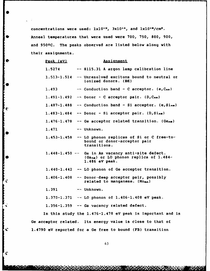
4. List of PL peaks observed .......................... 43
ix
* OPTICAL STUDY OF GERMANIUM,
GERMANIUM PLUS ARSENIC, AND GERMANIUM PLUS GALLIUM
IMPLANTS IN GALLIUM ARSENIDE
I. Introduction
A. Gallium Arsenide
In the world of semiconductors, the demand for ever
faster devices continues. Although the fastest devices in
existing computers can switch on and off in a billionth of a
second (1:80), still faster devices are needed in areas such
as supercomputers and microwave frequency communication
systems. With faster devices, new kinds of radars and
communication satellites could operate In the microwave band
and higher still.
Part of the process of developing better and faster
devices is the characterization of different semiconductor
materials. In the past, much of the emphasis has been focused
on silicon (Si) and germanium (Ge) for application inC-integrated circuit technology. One way to make semiconductor
devices operate faster is to use traditional materials such as
Si and make devices smaller, causing a reduction in the
distance an electron has to travel in a circuit. This has
been the traditional approach.
A different approach is to increase the velocity of the
electrons that flow through the semiconductor. To do this,
L1
IC
C
different material other than the traditional Bi needs to be
* employed. Gallium Arsenide (GaAs) is rapidly becoming the
semiconductor compound of choice for this new role.
GaAs offers some advantages over Si. GaAs is "fast".
*Q The electrons in GaAs behave as if they have a smaller mass
than those in a Si crystal. Thus, when an electric field is
applied to GaAs, The electrons will be accelerated faster than
* in Si. At its conduction band minimum, the GaAs electron has
a small effective mass (me*) equal to 0.07 times the mass of a
free electron (mE) outside the crystal. On the other hand,
for Si, mw*=(0.2)mE at its lowest value.
Other inherent characteristics of GaAs that make it
attractive include its electron mobility (up to 6 times that
* of Si), and its energy band structure. The conduction band
and valance bands in GaAs are separated by a band gap of 1.52
eV at 0 K. In Si the band gap minimum is 1.1 eV. GaAs
* devices are thus able to operate at higher temperatures than
Si, due to the reduction of noise caused by electrons that are
thermally excited into the conduction band. Because the
C conduction band minimum in GaAs is found at the zero value of
momentum of an energy-momentum Brillioun zone curve, GaAs is
known as a "direct-gap" semiconductor. Electrons do not need
any momentum from the lattice to make the lowest energy
transitions. On the other hand, Si Is "Indirect-gap" because
the lowest energy state in the conduction band is found at
Cnonzero values of momentum. The fact that GaAs is direct-gap
2
e
and that it is "fast", allows it to sustain electrical
oscillations in the microwave band which extends to 30
gigahertz. If someday GaAs device technology allows reduction
in gate lengths to a quarter of a micrometer or less, GaAs
devices will be able to operate in the millimeter-wave band
which extends from 30 to 300 gigahertz, and is now largely
unexploited. (1:87) The direct-gap structure of GaAs also
allows it to emit photons efficiently and as a result has made
GaAs important in the fabrication of laser diodes and light-
emitting diodes.
eB. Germanium Implanted Gallium Arsenide
By doping GaAs with different types of impurity atoms,
different characteristics of the material are achieved. Using
* Ge as a dopant in GaAs is interesting because as a Group IV
element, it is an amphoteric dopant, i.e., it can occupy
substitutionally a Ga or an As lattice site. Ge has often
* been used to produce n-type GaAs in a vapor-phase epitaxy
growth method and p-type samples in liquid-phase epitaxy. Ge
is used as a dopant in epitaxial layers due to its low
C, diffusion coefficient. GaAs doped with Ge has been used to
fabricate p/n junctions and p/n multilayers (2,3).
Recently, ion implantation of impurity dopants into semi-
insulating GaAs substrates has been widely used in the
fabrication of various electronic and opto-electronic devices.
Ge ion implantation has been used to produce reliable and
c reproducible ohmic contacts to n-type GaAs (4). As a method
3
(.W
of doping, ion implantation offers good prospects due to
the control one has over various implantation parameters.
Control is achievable over the impurity concentration and its
depth profile allowing for good reproducibility and
uniformity. However, processing after implantation Is made
more difficult because samples that are ion implanted must be
thermally annealed to remove the damage to the crystal caused
by ion bombardment.
In Ge implanted GaAs, n-type or p-type electrical
activity depends on impurity dose concentration and anneal
temperature (5). The electrical properties may be further
It altered by dually Implanting Ga or As with Ge. Electrical
investigation has shown that dual implantion of Ge and As
enhances n-type behavior, while dual implantion of Ge and Ga
enhances p-type behavior (6,7).
C. Objective and Scope
* Preliminary photoluminescence studies of Ge implanted
GaAs (GaAs:Ge) have been made by Yu (8). The objective of
this thesis is to examine a wide assortment of GaAs:Ge,
GaAs:Ge+As, and GaAs:Ge+Ga samples through photoluminescence.
The amphoteric behavior of Ge implanted into GaAs and its
relation to observed photoluminescence peaks is of
4particular interest. GaAs samples implanted singly with Ge,
dually implanted with Ge and As, and dually implanted with
Ge and Ga are all investigated and compared with previous
electrical and photoluminescence studies.
4
The substrate material used is <100> oriented Cr-doped
semi-insulating GaAs obtained from Crystal Specialties, Inc.
All ion implantation occured at room temperature at an ion
energy of 120 keV. Impurity dose concentrations ranged from
lx101 3 to lxl0'/cm2. Dually implanted samples were
implanted sequentually in equal doses and at the same energy
with Ge being implanted first. The samples were annealed at
varying temperatures from 700 to 9500C.
5
(.
e
A. Intrinsic Semiconductor Enerav States
Individual atoms have characteristic discrete energy
* levels of electrons surrounding the atom's nucleus. When a
number of atoms are brought together to form a semiconductor
crystal, the discrete energy levels of the electrons broaden
into regions of allowed electronic states or energy bands. An
intrinsic semiconductor Is characterized by these energy
bands. McKelvey (10:Ch 8) derives the band structure of an
*intrinsic semiconductor using a tight-binding approximation
and a nearly free electron approximation. Other approximation
techniques exist, and the use of one over the other depends on
* the type of semiconductor involved.
The outermost, or valence electrons of individual atoms
become the valence band of the semiconductor. The valence
* band, which consists of almost completely filled energy states
is used in chemical bonding and essentially provides the
structure to hold the crystal together. Higher allowed energy
states occur in the semiconductor band structure, and these
are known as the conduction band. The conduction band Is
almost completely empty. The valence and conduction bands are
eseparated by a region of forbidden energy states called the
band gap.
An ideal intrinsic semiconductor does not contain
c. impurities or defects within its lattice structure. The band
6
gap is completely empty of allowed electronic energy states.
If enough energy is provided through thermal energy, applied
voltage, or photons, such that the amount of energy is equal
to or greater than the band gap, an electron from the valence
band can transit to the conduction band. In such a
transition, a free electron is created in the conduction band,
while a positively charged free hole is created in the valance
band. Because electrons in the conduction band and holes in
the valance band do not take part in the binding of the
crystal lattice, they are free to move through the crystal and
constitute electrically active carriers.C
GaAs is known to have spherically symmetric, parabolic
bands near the bottom of the conduction band and the top of
the valence band. The minimum band gap corresponds to
conduction and valence band extrema located at the same point
in momentum space, i.e. k=O, making it a direct gap
semiconductor. The band gap has an energy value of 1.52 eV at
OOK.
B. Extrinsic Semiconductors
CSemiconductors can contain impurities, whether introduced
intentionally or not. If the impurities lead to overall
negative or positive electrical activity of a semiconductor,
-C these are known as extrinsic semiconductors. Doping with
impurity atoms allows one to control the number of active
carriers in a semiconductor. An impurity atom can occupy
C substitutionally the lattice site of a substrate atom.
7
When the number of electrons in the valance shell of
the dopant is less than that of the substrate atom that it
replaces, the dopant atom is known as an "acceptor". An
acceptor introduces an extra hole due to its lack of one
electron. Acceptors can therefore attract and accept a free
electrons from the lattice. If acceptors dominate in semi-
conductors, it is known as p-type (or positive type) material.
When the number of electrons in the valence shell of the
dopant is greater than that of the substrate atom it replaces,
a dopant atom is known as a "donor". Donors introduce extra
electrons into the lattice. If donors dominate in a semicon-
ductor, the material is known as n-type (or negative type).
Unlike the intrinsic semiconductor, extrinsic semiconduc-
tors have energy levels that exist in the band gap due to
donor and acceptor impurities. Because a donor has an extra
electron, it takes much less energy to ionize that electron
and free it to the conduction band than it does for a
transition to occur from the valence band to the conduction
band. It also takes less energy for an electron to transit
from the valance band to an acceptor than it does from the
valance band to the conduction band. An energy level struc-
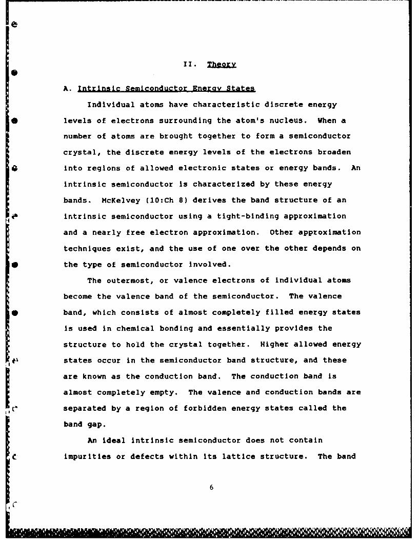
ture for an extrinsic semiconductor is shown in Fig. 1.
8
i
Conduction Band
. . . . . . . . . . Donor levelES
- 4- Acceptor level+ + + + +4++ + + + + + + + ++ 4+ +
+ + + + + + Valence Band+ + + + + + + +
Fig. 1 Donor/Acceptor states located within the band gap.
* The electron or hole ionization energy can be
approximated by a hydrogen-like approximation for both donors
and acceptors. Their ionization energies (Ex), are given by:
E1 =(e4m*/2X2 %
2 ) (1)
where e is the electronic charge, m* is the effective mass of
the electron or hole, X is the dielectric constant, and 1 is
• Planck's constant divided by 2K.
The energy required to activate holes or electrons will
vary, depending on the type of impurities present in the
• substrate and the type of semiconductor substrate used. For
GaAs, a hydrogen-like approximation yields a donor ionization
energy of 5.2 meV and an acceptor ionization energy of 34 meV
c for simple centers (11:327). A simple center is defined as an
impurity that sits on the Ga or As lattice site and
contributes only one additional carrier to the binding.
C. Amohoteric Behavior
Common semiconductor materials of interest include those
made of an element from Group li1A of the periodic table
combined with those of Group VA, which are called III-V
9
compounds. In their p-shells, Group III atoms contain one
* valence electron, while Group V atoms contain three. When
these atoms bond together, the three Group V electrons are
shared with the one Group III electron to form two covalent
* bonds.
If an element from Group IV of the periodic table is
doped into a semiconductor made of III-V material, it can
* substitutionally occupy either a lattice site of the Group III
element or that of the Group V element. This is known as
amphoteric behavior. A Group IV atom contains two valence p-
lshell electrons. If it occupies a Group III lattice site, an
extra electron is present, making it a donor. If it occupies
a Group V lattice site, an electron is lacking, making it an
* acceptor. Thus the Group IV dopant can behave as either an
acceptor or a donor. Whether or not the Group IV atom
replaces the Group III or Group V element depends on
* implantation parameters such as dopant dose, the temperature
at which the semiconductor is annealed, and the combination
of dopants used.
C Ge is known to be an amphoteric dopant in GaAs. Using
photoluminescence as a diagnostic tool, the amphoteric
behavior of Ge in GaAs is the main theme of this thesis.
D. Other Impurities and Defects
Besides those intentionally implanted or doped, other
impurities are found to exist within the substrate. These canc
result from contaminants introduced in the process in which
10
I,'jj
the substrate is grown or from other processing techniques
* such as capping and annealing that take place after crystal
growth. These inherent impurities can cause respective donor
and acceptor energy levels within the band gap.
* Several other types of defects can also be introduced
into the substrate as a result of fabrication and processing.
An impurity atom that lodges in a non-lattice site is an
interstitial defect, while the abscence of a substrate atom in
its respective lattice site is known as a vacancy defect. If,
for example, a Ga atom occupies an As site or vice versa, it
e is known as an anti-site defect. These defects are also known
as point defects. Defects can cause energy levels within the
band gap, and because they are usually too broad and too deep
in the band gap to be approximated by the hydrogenic
approximation, they are known as "complex centers"(11:359),
whereas shallow impurity levels are often simple centers and
* are approximated by the hydrogenic approximation.
E. Ion ImDlantation
In semiconductor fabrication, it is desirable to control
various parameters associated with the doping of impurity
atoms. In the growth of GaAs, introducing the dopant during
the growth process as in liquid phase epitaxial (LPE) growth,
vapor phase epitaxial (VPE) growth, etc., have had limited
success in the control of the doping parameters. A method
such as diffusing the impurity into a heated substrate((thermal diffusion) that is used with silicon substrates has
11
c2
not been developed for GaAs.
* Ion implantation, on the other hand, offers advantages
such as control over impurity concentration, uniformity,
reproducibility, various depth profiles of the Implanted
Impurity, selective area implantation through masking, lower
annealing temperatures, only slight lateral spreading,
application in planar type devices, and the prospect of high
* yields at low cost. The objective of ion implantation is to
develop a reliable, reproducible, and precisely predictable
doping result. Ion implantation is used in several types of
iGaAs devices such as microwave devices, optoelectronic devices
and solar cells.
Ions are implanted into the near surface region of a
* substrate by accelerating the ions to a high velocity and then
directing them in a beam to the surface of the semiconductor.
The ions' mass, velocity and particle flux are used to control
* the impurity concentration and its depth profile (12:109).
As a result of implantation, damage occurs in the
substrate and defects are introduced. Crystalline defects
such as point defects, clusters of point defects, dislocations
and dislocation loops, and stacking faults are produced in the
substrate. To reduce this problem, thermal annealing is
required and this results in a reduction in the number of
defects. In this experiment annealing was done at
temperatures of 700 to 9500C. Because of the tendency of
substrate elements such as As in GaAs to out-diffuse during
12
annealing and cause surface decomposition, encapsulation is
required during the annealing process. Silicon nitride0
(Si=N4) is the common encapsulant used.
F. Dual Imolantation
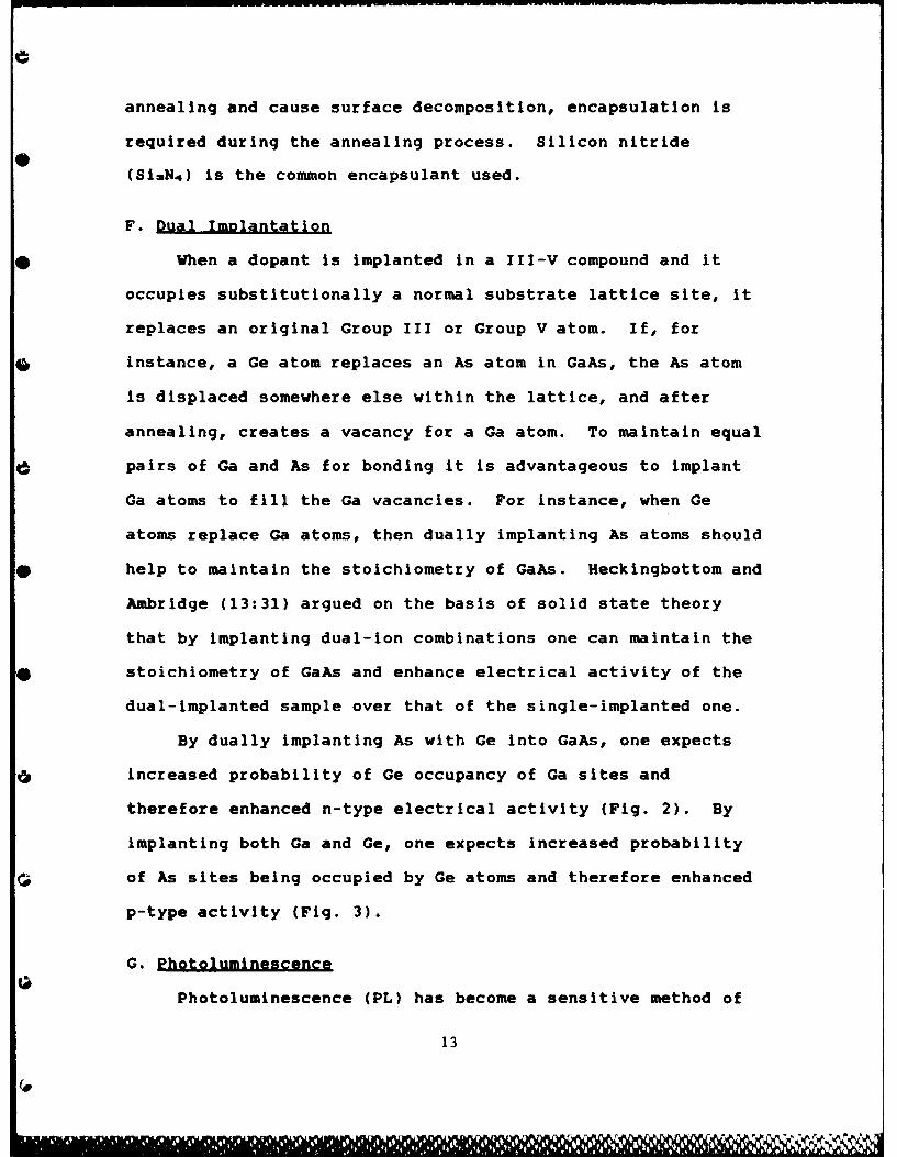
* When a dopant is implanted in a III-V compound and it
occupies substitutionally a normal substrate lattice site, it
replaces an original Group III or Group V atom. If, for
*instance, a Ge atom replaces an As atom in GaAs, the As atom
Is displaced somewhere else within the lattice, and after
annealing, creates a vacancy for a Ga atom. To maintain equal
pairs of Ga and As for bonding it is advantageous to implant
Ga atoms to fill the Ga vacancies. For instance, when Ge
atoms replace Ga atoms, then dually implanting As atoms should
* help to maintain the stoichiometry of GaAs. Heckingbottom and
Ambridge (13:31) argued on the basis of solid state theory
that by implanting dual-ion combinations one can maintain the
* stoichiometry of GaAs and enhance electrical activity of the
dual-implanted sample over that of the single-implanted one.
By dually implanting As with Ge into GaAs, one expects
increased probability of Ge occupancy of Ga sites and
therefore enhanced n-type electrical activity (Fig. 2). By
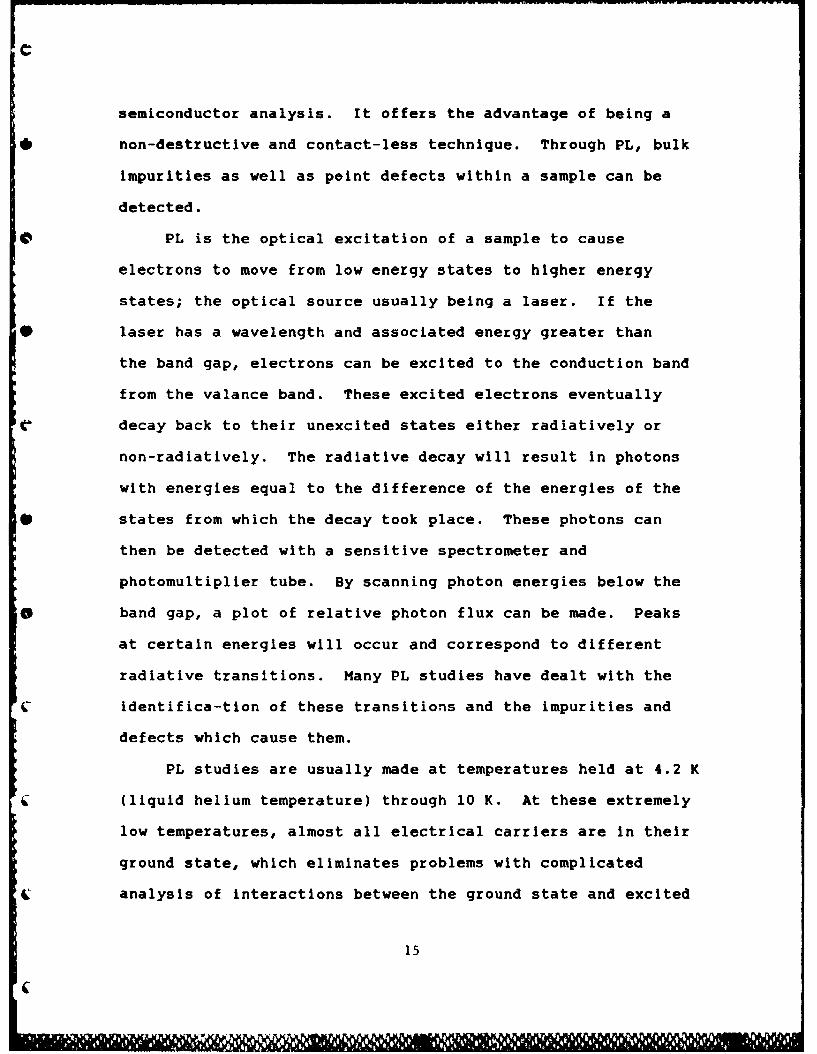
implanting both Ga and Ge, one expects increased probability
of As sites being occupied by Ge atoms and therefore enhanced
p-type activity (Fig. 3).
G. Photoluminescence
Photoluminescence (PL) has become a sensitive method of
13
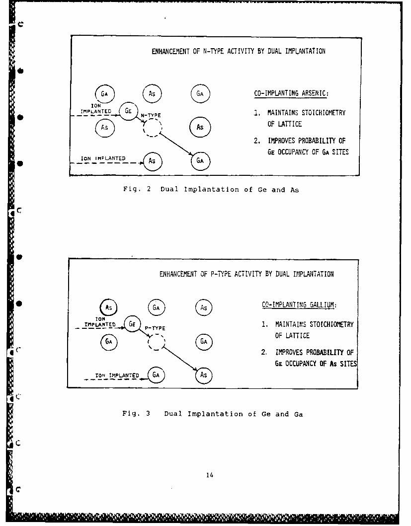
ENHANCEMENT OF N-TYPE ACTIVITY BY DUAL IMPLANTATION
OA OSCO-IMPLANTING ARSENIC:
'ONIPL A TED GE* --- N-TYPE 1. MlAINTAINS STOICHIOMETRY(~) -(~j)OF LATTICE
2. IMPROVES PROBABILITY OF_____GE OCCUPANCY OF GA SITES
ION IMPLA&NTE2 _ As
Fig. 2 Dual implantation of Ge and As
ENHANCEMENT OF P-TYPE ACTIVITY BY DUAL IMIPLANTATION
S* CO-IMPLANTING GALLIUM:
ION-IMPLANTE I GE P-YE1. MAINTAINS STO!CHIOMETRY
OF LATTICE
C 2, IMPROVES PROBABILIT OF
GE OCCUPANCY OF As SITErON IMPLANTED C As
Fig. 3 Dual Implantation of Ge and Ga
14
semiconductor analysis. It offers the advantage of being a
non-destructive and contact-less technique. Through PL, bulk
impurities as well as point defects within a sample can be
detected.
*PL is the optical excitation of a sample to cause
electrons to move from low energy states to higher energy
states; the optical source usually being a laser. If the
*laser has a wavelength and associated energy greater than
the band gap, electrons can be excited to the conduction band
from the valance band. These excited electrons eventually
decay back to their unexcited states either radiatively or
non-radiatively. The radiative decay will result in photons
with energies equal to the difference of the energies of the
* states from which the decay took place. These photons can
then be detected with a sensitive spectrometer and
photomultiplier tube. By scanning photon energies below the
o band gap, a plot of relative photon flux can be made. Peaks
at certain energies will occur and correspond to different
radiative transitions. Many PL studies have dealt with the
identifica-tion of these transitions and the impurities and
defects which cause them.
PL studies are usually made at temperatures held at 4.2 K
(liquid helium temperature) through 10 K. At these extremely
low temperatures, almost all electrical carriers are in their
ground state, which eliminates problems with complicated
analysis of interactions between the ground state and excited
15
C
states. Low temperatures also reduce non-radiative
transitions due to thermal processes, and reduce thermal line
broadening making discrimination between different peaks more
apparent.
Lasers are usually used as the source of optical
excitation due to their localized spatial resolution and
ability to select one coherent wavelength line from a variety
available. Because laser lines of different wavelengths have
different penetration depths into the sample, one can select
an appropriate sampling depth to probe by just choosing a
corresponding laser line. A Krypton-Ion laser with a
wavelength of 647.1 nm has a penetration depth of about 3000 A
in GaAs (8:7167). For ion implanted GaAs, it is important
that the laser penetrate the ion implanted layer to identify
the extrinsic PL peaks. The peak projected range of Ge
implants in GaAs is 464 A with a standard deviation of 173 A
at 120 keV. The Ge distribution is from 0 to 2400 A
(8:7165,7167). So a laser with X=647.1 nm will more than
penetrate the implanted layer.
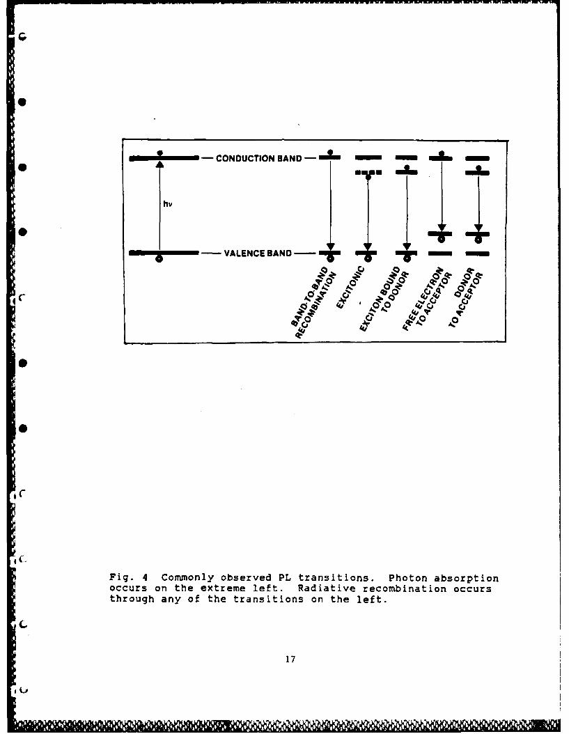
C H. Radiative Transitions
A radiative transition occurs when an electrons in an
excited energy state decays to a lower energy state and emits
energy in the form of photons. The fundamental and most
commonly observed PL transitions are illustrated in Fig. 4.
They are band-to-band recombination, excitonic (free exciton
C recombination), free electron to acceptor (free-to-bound), and
16
4wg
inJ.EEEE CONDUCTION BAND-EELS
-VALENCE BAND-
",_q,
04
Fig. 4 Commnonly observed PL transitions. Photon absorptionoccurs on the extreme left. Radiative recombination occursthrough any of the transitions on the left.
17
donor-to-acceptor.
1. Band-to-Band Recombination
An electron in the conduction band that directly
recombines with a hole in the valence band makes a band-to-
band transition. The photon energy emitted in the process is
equal to Em, the band gap energy. This transition is rarely
seen in materials with small effective masses such as GaAs
(14:173).
2. Exitn
An electron and a hole can combine in such a way
that they will orbit around each other due to coulombic
attraction. This electron-hole pair is called an exiton.
Because the exciton has such a small ionization energy, it is
observed only at low temperatures. The Schr8dinger equation
for the exciton is analogous to that of the hydrogen atom, and
gives solutions of the form:
Ex=(-Ae4/2%2X2 n2 ) (2)
where p is the reduced mass of the respective effective masses
of the electron-hole pair, e is the electronic charge, A is
Planck's constant divided by 2n, K is the dielectric constant,
and n is the quantum number describing the exciton state. For
an unbound exciton that is free to move through the lattice,
the expected value for the electron-orbital radius is:
<r>,=( n2 a.KXm/ma*) (3)
where a. is the Bohr radius (0.53 A) and ma* is the effective
mass of the electron.
In GaAs, X=12.5 and mrw/mz=0.0065. The expected value of
18
the orbital radius for n=1 is then <r>,=1040 A. This radius
* is extremely large due to the small in" and extends over
thousands of Bohr radii! (14:173)
a. Free Exciton Transitions
* An electron-hole pair that is free to move
through the lattice is known as a free exciton. When the
electron and hole recombine, a transition occurs where a
*• photon is emitted. The photon energy is given by:
hV=Ee-Ex (4)
where E. Is the band gap energy value, and Ex is the excitonic
energy as given in eqn. (2). Therefore a free exciton can
have recombination energy up to (pe4 /2K 2X2 ) less than Es.
In GaAs, the higher free exciton states are not always
*distinguishable. The ground state free exciton, however, can
sometimes be distinguished as a narrow peak at 1.515 to 1.5153
eV (15:464).
• b. Bound Exciton Transitions
The presence of an impurity can sometimes
increase the binding energy of an exciton, making it more
energetically favorable to remain in the vicinity of the
impurity. This situation is called a "bound" exciton. When
the electron and hole of a bound exciton recombine, the photon
energy is given by the modified equation (4):
hV=E*-Ex-E. (5)
where B. Is the additional binding energy which depends on the
C Impurity to which the exciton is bound.
19
'A gIIIIIIII U 1'1
All exciton peaks disappear rapidly with increasing
temperature. Bound excitons will first free themselves of the
impurity and then dissociate into individual electrons and
holes due to thermal ionization.
3. Free-to-Bound Transitions
Free-to-bound (FB) transitions, also known as band
impurity transitions, can either be a transition from the
donor level to the valence band or a transition from the
conduction band to the acceptor level. The photon energy from
such a transition is simply:
hV=Eo-Ez (6)
where Ex is the same as in eqn. (1) and can be written as ED
for conduction band to donor level and EA for acceptor level
to valence band. Typically ED ranges from 5 to 7 meV for
shallow donors (14:177). Because the donor levels are so
close to the band edge, it is difficult to identify them
unambiguously. Usually free-to-bound PL studies are
necessarily limited to free electron to acceptor transitions.
As impurity concentrations are increased, donor or
acceptor levels tend to broaden into a band of states (16:135-
136) due to overlapping of the wave functions of electrons.
This can make identification of different impurity peaks more
difficult.
4. Donor-Acceptor Pair Transitions
When donors and acceptors are simultaneously present
in the material, the impurities often form a pair known as a
donor-acceptor pair (DAP). The normal ionization energy is
20
po
reduced by the coulombic interaction between the electron of
the donor and the hole of the acceptor. The recombination
photon energy Is then:
hV=Eo-EA-ED+(e2/Xr) (7)
where B., E^, and ED are as defined previously, X is the
dielectric constant, and r is the separation between
impurities. Note that the last term represents the coulombic
interaction.
If it is assumed that most of the impurities are
substitutional and located at lattice sites, the separation r
will take on discrete values depending on the statistical
distribution of the impurities. As a result, a series of
sharp DAP lines can often be observed corresponding to the
discrete values of r. Contributions from distant pairs will
be unresolvable and merge into a broader peak.
If the activation energies EA and ED are quite small,
only recombinations at relatively distant DAP give bound
states according to eqn. (7), and the discrete series of lines
are not observed, leaving only the broader peak of the distant
pairs (17:119). Discrete DAP lines are not observable in GaAs
because EA Is modest and ED very small.
Williams and Bebb (11:336) list several characteristics
that give evidence for DAP emission:
a) A shift to higher energies as the excitationIntensity increases (about 1 meV per decade ofexcitation intensity in GaAs).b) Narrowing of the emission band with increasingintensity.c) A shift to higher energies as the donor
21
(9
C
concentration increases.d) A rapid decrease in intensity as the temperatureincreases from 25 to 35 K.
* e) A shift to higher energies with increasingtemperature (line broadening occurs also).
It is also interesting to note that with high doping
levels or increases in temperature that the near band gap
luminescence will usually show larger FB peaks than DAP peaks
in GaAs.(17:145-6)
5. Phonon Assited Transitions
All optical transitions must conserve both energy and
momentum. In an indirect gap semiconductor, this means that
phonon coupling with the lattice is required for minimum
energy transitions. In GaAs, which is direct gap, no phonon
assistance is required to conserve momentum. However, phonon
coupling can occur and resulting radiative transitions atS
lower energies can be found in GaAs. As the binding energy of
an electron or hole bound to an impurity gets stronger, its
interaction with lattice vibration increases. This non-
radiative process then reduces the energy released in the
radiative transition. In GaAs, the longitudinal optical (LO)
phonon coupling is by far the strongest, and can reduce
radiative transitions by integer multiples of 36(±2) meV
(11:387-8). Any number of lower energy replicas of near band
gap peaks may be observed in a given GaAs PL spectrum.
22
C
III. Previous Work
A. Photoluminescence
A previous PL study has been made on Ge implanted
* GaAs. Yu (8) studied Ge implanted GaAs as a function of
exciting wavelength, excitation intensity, temperature, and
depth of the implanted layers. Yu used Cr-doped semi-
* insulating GaAs substrates that were implanted at room
temperature at an energy of 120 keY.
The study by Yu included first of all a control substrate
with PL peaks which were assigned as follows:
1.514 eV -- Due to unresolved excitons and a donorto valence band transition
1.488 eV -- Due to Si acceptor in the substrate
* For Ge implanted samples the following peaks were
observed as the dose was varied from 5 x 10¹² to 3 x 10¹⁵/cm2
and were assigned as follows:
A) 1.468-1.480 eV -- Donor-Ge acceptor pair transitionB) 1.43-1.46 eV -- Donor-Ge acceptor pair modified by
a random impurity potentialC) 1.435 eV -- As vacancy-Ge acceptor complexD) 1.38 eV -- Ga vacancy-deep acceptor transitionE) 1.18 eV -- Ga vacancy-Ge donor complex
In addition, Yu made the following conclusions:
1) The As vacancy-Ge acceptor complex emission was
dominant in the near surface region (0-300 A), the donor-Ge
acceptor pair emission was dominant in the region 300-1000 A,
and the Si acceptor related emission was dominant in the
region 1000-3000 A.
2) Emissions due to the donor-Ge acceptor pair are
23
C
present in all Ge-implanted layers.
*• 3) The binding energy associated with the Ge acceptor is
40±3 meV.
* B. Electrical Measurements
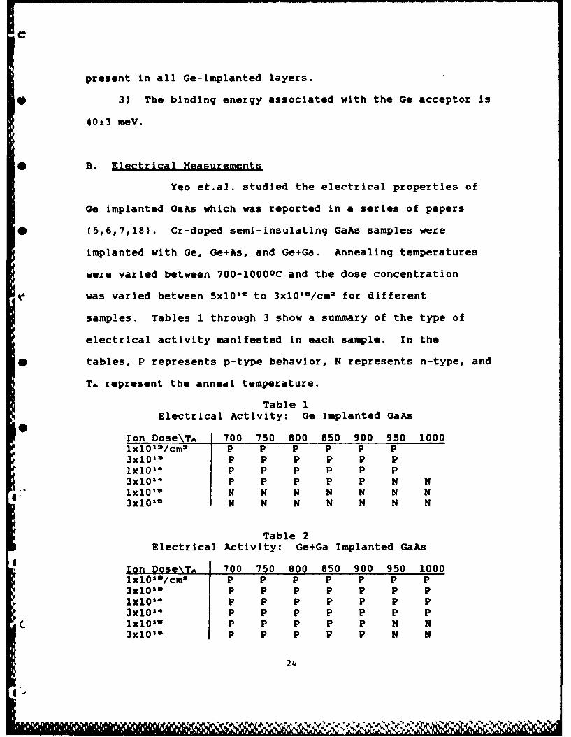
Yeo et.al. studied the electrical properties of
Ge implanted GaAs which was reported in a series of papers
* (5,6,7,18). Cr-doped semi-insulating GaAs samples were
implanted with Ge, Ge+As, and Ge+Ga. Annealing temperatures
were varied between 700-10000C and the dose concentration
was varied between 5x10¹² to 3xl01 s/cm 2 for different
samples. Tables 1 through 3 show a summary of the type of
electrical activity manifested in each sample. In the
* tables, P represents p-type behavior, N represents n-type, and
T^ represent the anneal temperature.
Table 1Electrical Activity: Ge Implanted GaAs
Ion Dose\TA 700 750 800 850 900 950 1000x 10 2'/cm" P P P P P P
3x10l 3 P P P P P P1x10 14 P P P P P P3x10' 4 P P P P P N Nlx10 1 N N N N N N N3x1016 N N N N N N N
Table 2Electrical Activity: Ge+Ga Implanted GaAs
Ion Dose\T. 700 750 800 850 900 950 1000lxlO'3'/cma P P P P P P P3x1012 P P P P P P Plx10' 4 P P P P P P P3x1011 P P P P P P P
- lxlO"S P P P P P N N3x10' P P P P P N N
24
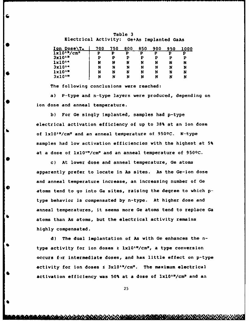
Table 3Electrical Activity: Ge+As Implanted GaAs
0Ion Dose\TA 700 750 800 850 900 950 1000lx1013/cm2 P P P P P P P3x10'2 P P P P P P PlxlO'1 N N N N N N N3x10 N N N N N N N
S1x10 1 N N N N N N N3x10 s N N N N N N N
The following conclusions were reached:
a) P-type and n-type layers were produced, depending on
ion dose and anneal temperature.
b) For Ge singly Implanted, samples had p-type
electrical activation efficiency of up to 38% at an ion dose
of lxlO'3 /cm2 and an anneal temperature of 9500C. N-type
samples had low activation efficiencies with the highest at 5%
at a dose of lxlO'O/cm 2 and an anneal temperature of 9500C.
c) At lower dose and anneal temperature, Ge atoms
apparently prefer to locate in As sites. As the Ge-ion dose
and anneal temperature increase, an increasing number of Ge
atoms tend to go into Ga sites, raising the degree to which p-
type behavior is compensated by n-type. At higher dose and
anneal temperatures, it seems more Ge atoms tend to replace Ga
atoms than As atoms, but the electrical activity remains
highly compensated.
d) The dual implantation of As with Ge enhances the n-
type activity for ion doses a lxlO'U/cm2 , a type conversion
occurs f~,r intermediate doses, and has little effect on p-type
activity for ion doses 5 3xlO'/cm2 . The maximum electrical
activation efficiency was 50% at a dose of lxlOIO/cm2 and an
25
anneal temperature of 9500C for p-type samples, while it was
* 24% at a dose of 3xl0'4/cm2 and an anneal temperature of
10000C for n-type samples.
e) The dual implantation of Ga with Ge enhances the p-
* type activity for ion doses 5 3xl0'4/cm2 , while the original
n-type activity of Ge singly implanted changed to p-type for
doses z lxlOs/cm, except for anneal temperatures > 9000C.
* The maximum p-type activation efficiency was 68% at a dose of
1x10¹³/cM 2 and an anneal temperature of 9500C.
C
26
St
IV. Description of Experiment
A. Sample Preparation
The substrate material used was <100> oriented semi-
• insulating (SI) Cr-doped GaAs obtained from Crystal
Specialties, Inc. The substrate was grown by the Horizontal
Bridgman method. The sample size ranged from 1/4 to 3/16
* inch square wafers. Before ion implantation, the samples were
carefully cleaned with acquasol, deionized water,
trichloroethylene, acetone, and methanol and dried with
* nitrogen gas. Next, the samples were free-etched with an
H2 SO4 :30%H 202 :H2 0 solution in a 3:1:1 ratio by volume for 90
sec. Free-etching removes unwanted surface damage caused by
* crystal cutting and polishing.
Ion implantation was performed at an ion energy of 120
keV at room temperature. The incident ion beam was directed
* from a hot cathode source at 70 off the <100> crystal axis to
minimize Ion-channeling effects. Ion implantation took place
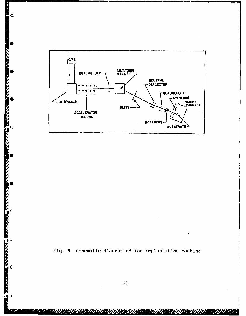
using a Varian/Extrion model 400-10AR ion implanter (Fig. 5).
b When dual implantation was accomplished, the doses and energy
were made equal and implanted sequentually. Implantation was
carried out at dose concentrations ranging from lxlO1 3 to
ixlO"U/cm 2.
After implantation, the samples were once again cleaned
and subsequently encapsulated with an approximately 1000 A
*layer of silicon nitride (Si3N4 ) in a cold-wall pyrolitic
27
* ANALYZINGQUADRUPOLE\ MAGNT NUTA
r T T " 7 1 DEFLECTOR
r rT QUA RPOLE
SLITS CHMBER
ACCELERATOR
COLUMNSCANNERSJ 4J
Fig. 5 Schematic diagram of Ion Implantation Machine
28
4MOM
reactor. The Si3N4 deposition took place in 35 sec. at 7000C,
the samples reaching 700C within 9 sec. (18:618).
Encapsulation was preparatory to thermal annealing and
prevented the tendency of As to outdiffuse, thereby protecting
the surface from decomposition via the encapsulant.
The samples were then annealed at various temperatures in
flowing hydrogen gas for 15 min. Anneal temperatures ranged
from 700 to 9500C. The samples were placed cap-side down on a
GaAs substrate to improve the performance of the encapsulant
at high anneal temperatures. No sign of surface degradation
could be observed by visual inspection (6:5786). Dissolution
of the encapsulant took place in 48% hydroflouric acid for 3
min. The samples were then given one final careful cleaning
using trichloroethylene, acetone, methanol and deionized
water; being blown dry with dichlorodiflouromethane gas.
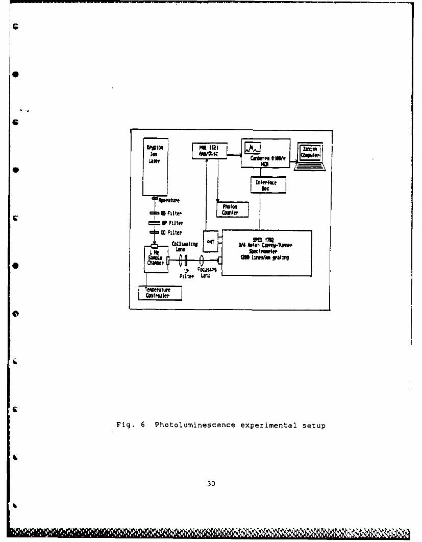
B. Photoluminescence Experimental Setup
*• Photoluminescence measurements were taken using the
experimental setup as shown in Fig. 6.
1. Excitation Source and Setuo
The optical excitation source used was a Spectra-
Physics series 2000 Krypton-ion laser. A single red line set
at 6741 A was used.
Most measurements were taken at a low laser power of 8 to
9 milliwatts (mW). However, certain data was taken at up to
80 mW. To achieve this, the laser was set in its constant
power mode at 200 mW with the plasma tube current running at
29
1 1 1 11
CMS
I'lLaw
r FP Filter00 Filter
LHe Le SICt PetPN O~r nwg a n ting
cntpoller
Fig. 6 Photoluminescence experimental setup
30
30 amps and the magnet current running at about 5 amps. After
the beam exited the laser aperture it was desired that stray
ultraviolet light be removed from the laser beam, so a 6500 A
narrow band-pass filter was placed in the beam's path. This
reduced the beam power to near 80 mW. To reduce the beam even
more, two 0.5 optical density filters were placed in the beam
path, reducing the laser power to approximately 8.5 mW. The
beam then passed through a mirrored optical periscope and was
directed through quartz windows into the cooled sample chamber
and onto the sample. The beam waist was approximately 2 mm in
diameter. As a result, the approximate power density for a
laser power of 8.5 mW was 0.27 W/cm2 . This was the usual
setting. At a power of 80 mW the maximum power density was
2.55 W/cm 2 .
2. ODtical Detection System
After the sample is optically excited by the laser,
photoluminescence is emitted and travels through the sample
chamber window. The PL is approximately collimated outside
the sample chamber by a lens (focal length= 70mm). The PL
then passes through a long-pass filter (passes X > 6650 A) and
then is focused through a second lens (f#=5) onto the
spectrometer entrance slit.
The PL emission was then dispersed with a SPEX 1702 3/4
meter Czerny-Turner Spectrometer. The grating used was blazed
for 5000 A at 170 27' and had 1200 lines/mm. The grating was
used fc first order diffraction. The spectrometer had linear
reciprocal dispersions of 10.24 to 9.70 respectively, for the
31
end values of the range from 8100 to 9320 A (19:19). The
* entrance and exit slit widths were 75 and 150 pm,
respectively. For maximum throughput, the exit slit should be
at least twice the entrance slit (19:20). The resulting
* average resolution was approximately 0.75 A or 0.125 meV in
the wavelength range mentioned.
At the beginning of each experimental run, the entrance
* and exit slits were set to 10 and 20 pm each, so that an argon
lamp could be used to calibrate the spectrum. The 8115.31 A
argon line was used as the calibration point. Immediately
after scanning this line the slits were set to 75 and 150 Um
to complete the run.
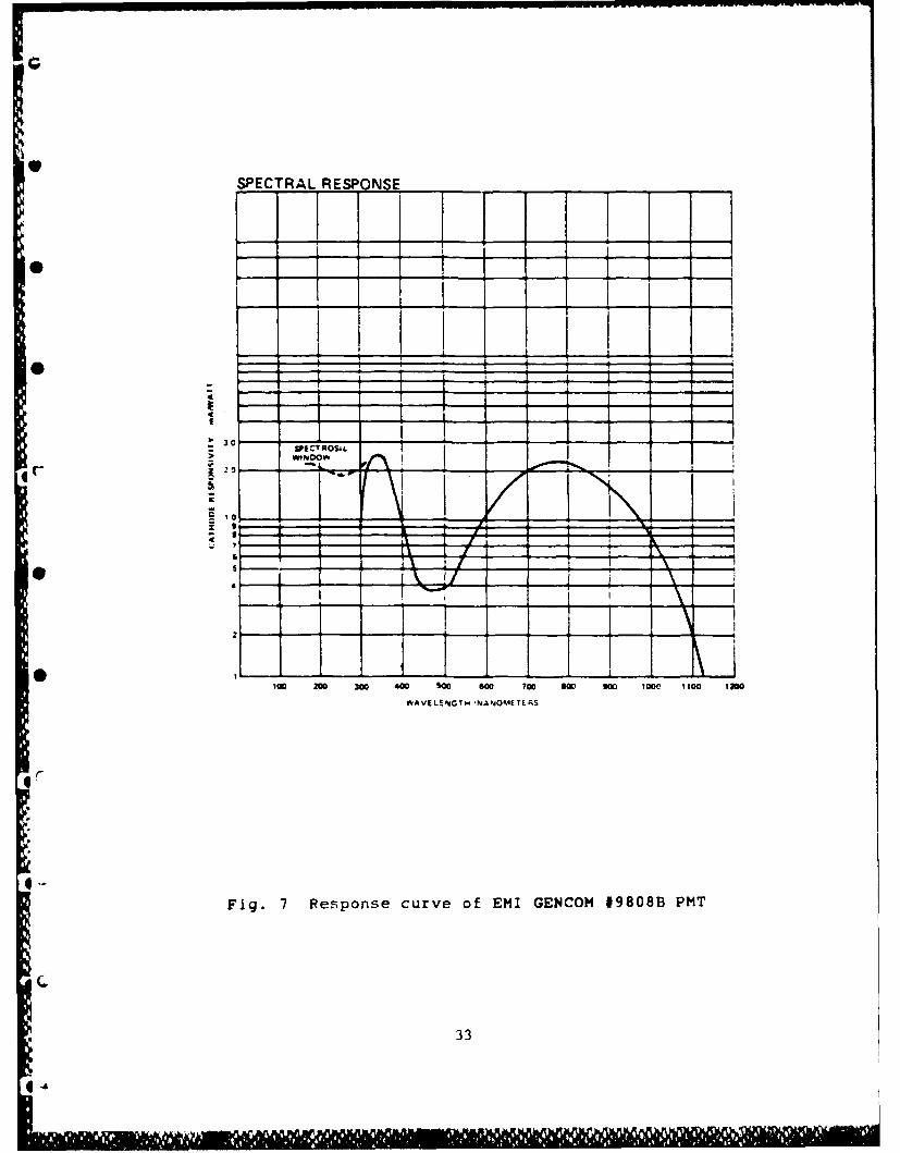
An EMI GENCOM #9808B Photomultiplier Tube (PMT) was
* connected to the exit slit of the spectrometer to collect the
dispersed PL. The PMT was liquid nitrogen cooled and employed
an S-1 type photocathode. The PMT's spectral response curve
* is shown in Fig. 7.
The PMT electrical signals were next sent to a Princeton
Applied Research (PAR) Model 1121A Amplifier/Discriminator
(AD) with a built in high voltage supply to run the PMT. In
order to achieve the best signal to noise ratio, threshold
controls on the AD were optimized for the desired wavelength
region.
At this point, a PAR Model 1112 Photon Counter/Processor
was used to get a real time look at photon counts. The
Cinitial photoluminescence alignment into the spectometer was
32
G
SPECTRAL RESPONSE
- - - T RS
4 1 1 I l1w- IL
=I ,I
4 \
100 200 "300 400 90 600 700 800 !10 10CC 1100 1200
bWAVEILtdGTMN ,NAOM£ TL S
.-
- Fig. 7 Response curve of EMI GENCOM 19808B PMT
-* 33
*I
made much easier by watching and optimizing the photon count
number.
The signal from the AD was next sent to a Canberra 8100/e
Multi-Channel Analyzer (MCA). In order to make the MCA
channel advance rate synchronous with the spectrometer scan
rate, an interface consisting of an external step motor driver
was used. The scan rate was set to scan at 0.434 A/channel
for all experimental runs.
It is important for the resolution obtained from the
electrical components of the optical detection system to be at
least as good as the resolution obtained from the spectrometer
(4:38). In this experiment the electronic component
resolution (0.434 A) was better than the spectrometer slit
resolution (0.75 A).
3. Sample Crvogenics
Photoluminescence is highly dependent on
temperature. At temperatures as high as room temperature a
great deal of the optical transitions cannot take place due to
excessive thermal excitation. A cryogenic system is used to
remedy this situtation and cool samples to near liquid heliumC
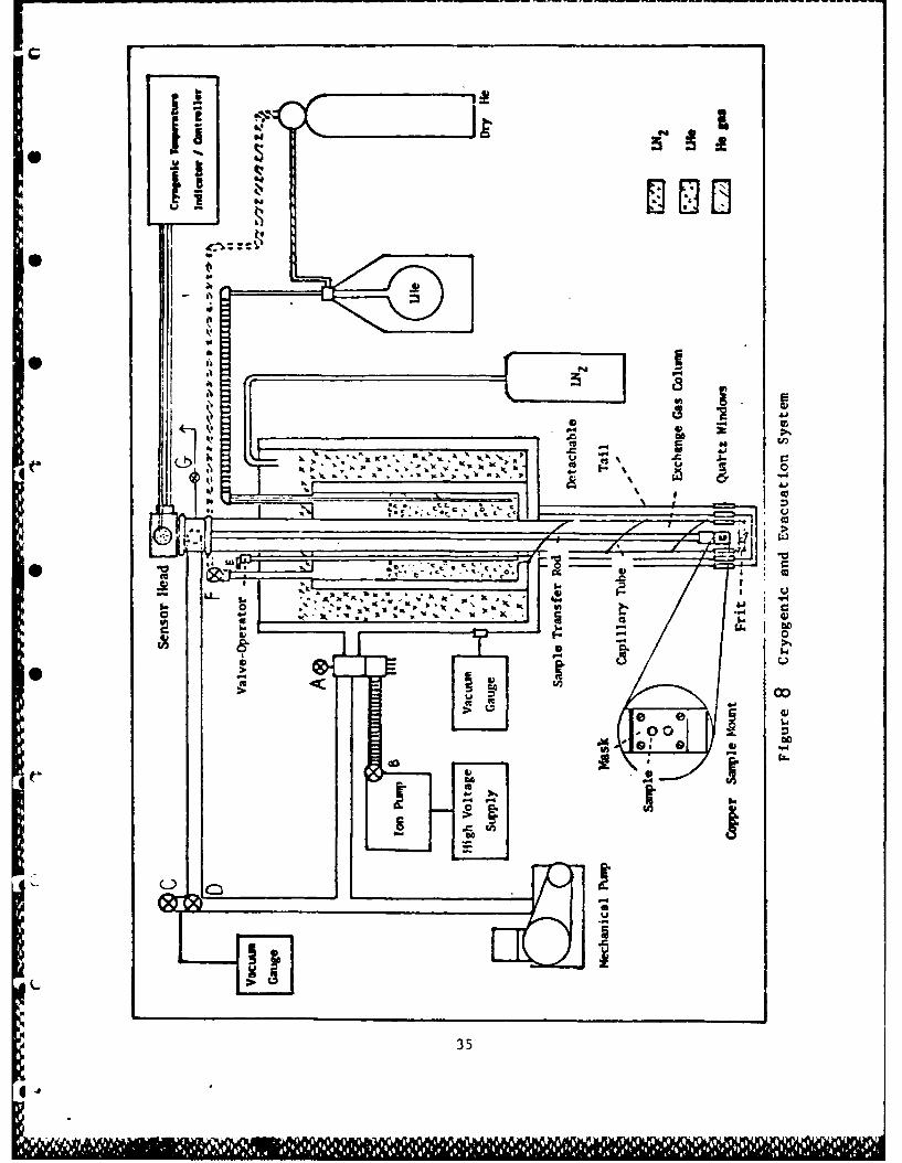
temperatures. An Andonian Cryogenics, Inc. cryostat was used
to cool the sample. A schematic of this cryostat and its
support vacuum pumps is shown in Fig. 8.
The cryostat consisted of an outer 4-liter liquid
nitrogen (LN2 ) reservoir and an inner 3-11ter liquid helium
(LHe) reservoir. Each reservoir is surrounded by a vacuum
chamber to Insulate from external temperatures and keep heat
34
e11
VC. ccI I vI Iw"
)k at I
000
6mm
35
transport to a minimum. The LN2 reservoir acted as a cold
buffer between the room temperature environment and the LHe
reservoir. As the LHe slowly boils off in its reservoir, the
cold liquid helium passes through a capillary tube into the
sample chamber located in the tail of the cryostat. The
sample is cooled by the evaporated helium. Care had to be
taken to control the needle valve to the capillary tube to
avoid flooding the sample chamber with LHe and avoid the
resulting interference due to turbulent boiling.
The following procedure was used in evacuating and
cooling the cryostat:
a) A mechanical roughing pump was used to evacuated the
vacuum chamber to about 10-3 torr by opening valve A.
b) Next, a forepump followed by a diffusion ion pump
evacuated the chamber to about 10-6 torr by opening valve B
and closing valve A.
c) The LHe reservoir is next flushed out with helium gas
through fill hole F, through the capillary tube into the
sample chamber, and out through the flowmeter (G). This is to
ensure that air and moisture are removed to prevent freezing
and blockage of the capillary tube and needle valve. A valve
at fill hole F is closed with a back pressure of helium gas.
d) LN2 was poured into its reservoir through a funnel
placed in the LN2 fill hole. A vent hole is opened during the
filling process. After filling completely, the reservoir is
allowed to settle and both holes are plugged with rubber
36
stoppers.
e) LHe was transferred through a transfer line into the
LHe fill hole. A vent hole was open during the process. Care
was taken to transfer slowly to avoid a volatile transfer.
There was indication that the transfer was complete when a
strong opaque plume caused by helium vapor was observed at the
vent hole.
f) Throughout an experimental run, the needle valve E
was adjusted to maintain a stable temperature.
Samples were inserted into the cryostat by first being
mounted on a sample finger. At the end of the sample finger
was a copper block. On opposing sides, cut into the copper
block, were square depressions to place the samples. Samples
were mounted with a small sticky film of GE varnish applied to
their backsides to prevent them from dislocating within the
sample chamber. Thin copper sheets containing circular
apertures 4 mm in diameter were placed over the samples in
the block and secured into place with two screws. The
circular apertures overlayed the center of each sample. The
sample finger with the mounted samples was then placed into
the center of the cryostat.
The temperature of the samples was monitored via a
temperature sensing diode that was attached to the sample
copper block. This in turn was connected to a Lakeshore
Cryotronics Temperature Controller. The temperature was
maintained at 4.5 to 5 K for most experimental runs.
37
V. Results and Discussion
The photoluminescence spectra of semi-insulating GaAs
can be difficult to evaluate. Crystals grown by the
* horizontal Bridgman method produce PL emission peaks that
are broad and the luminescent efficiencies tend to be low
(14:177). Peaks that are broad often hide information. In
*0 the measurements taken in this experiment, with the exception
of one run, peaks due to exciton transitions were always
unresolved. Also, peaks due to several different impurity
acceptor transitions could merge into one or two peaks,
leaving one with less ability to identify the peaks' origin.
However, more often than not, there was enough resolution in
* the measurements presented here to distinguish and compare
important acceptor related peaks.
A. Control Substrate
An unimplanted, uncapped, unannealed sample of Cr-doped
semi-insulating GaAs was used as the control substrate. Its
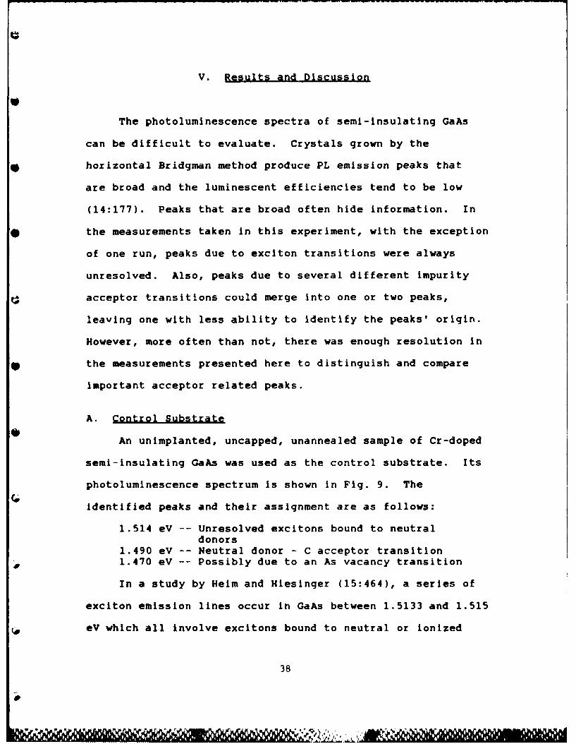
photoluminescence spectrum is shown in Fig. 9. The
identified peaks and their assignment are as follows:
1.514 eV -- Unresolved excitons bound to neutraldonors
1.490 eV -- Neutral donor - C acceptor transition• 1.470 eV -- Possibly due to an As vacancy transition
In a study by Helm and Hiesinger (15:464), a series of
exciton emission lines occur in GaAs between 1.5133 and 1.515
eV which all involve excitons bound to neutral or ionized
38
P. Gal 51 Substrate: unmp)apted wunarveoed
M6 8500 8340 82m0e~ [V Fr! FI fzjr,,r~p....., y .i...... v.I
GaAs SubstrateOEMA~ Laser at 's CVTemp at about i 2K
N
L4307 1.4SO 1470 ;.490
DO~GY [eV)
Fig. 9 PL spectrum of GaAs substrate. Sourceintensity: 2.4 W/cm2 -
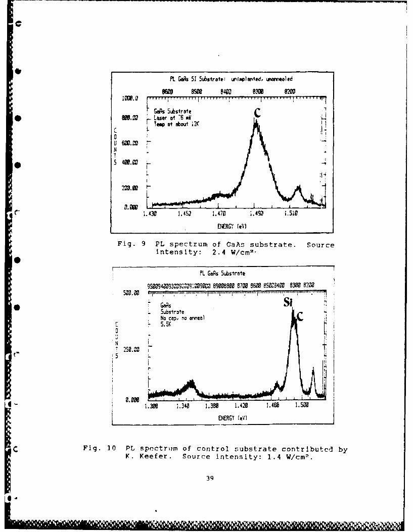
Pt GaAs Substrate
95009400932IJ921109 89088800 8700 8600 85008400 8300 620
* aes SiS ubstrate ana
- 5.5K
1.300 1.340 1.380 1.420 1.460 1.500
ENERGY [.VI
CFig. 10 PL spectrom of control substrate contributed byK. Keefer. Source intensity: 1.4 W/cm2.
39
Kzalam dl !.
e
donors. The exciton line observed in this control substrate
Is unresolved with a peak in the range ascribed to donor
bound excitons. Yu observed a similar peak and assigned it
as several unresolved excitons and a donor to valence band
transition (8:7165).
The next peak, 1.490 eV, is assigned as a neutral donor
to C acceptor peak. It is generally known that carbon is a
common residual impurity in GaAs grown in many different
methods. A donor-C acceptor peak is often observed at about
1.49 eV. In Cr-doped semi-insulating GaAs this peak was seen
at 1.490 eV by Swaminathan et. al. (20:159). Keefer also
observed this peak at 1.491 eV In LEC grown GaAs (21).
It is probable that because of its broadness, the 1.490
eV peak Is an unresolved combination of the C-related peak and
a conduction band to Si acceptor transition. In the contol
substrate in Yu's study, a large emission band assigned as a
Si acceptor related peak was observed at 1.488 eV. The
samples used by Yu were similar to those used in this study.
Measurements taken by Keefer with a similar control substrate,
using the identical experimental equipment used in this study,
resulted in the spectrum shown in Fig. 10. A peak due to Si
at 1.487 eV is evident and merges in such a way that a
shoulder due to C is present at 1.491 eV. As will be seen
later, the Si related peak was always observed in implanted
samples used in this study, and usually dominated the C
related peak. In implanted samples, the SI related peak was
probably enhanced due to the fact that a SiN4 encapsulant was
40
p
G
used during the annealing process. Yu, in another study
* (22:5046), reported that in n-type GaAs substrates that had
been heat treated and encapsulated with SimN4 , "acceptors in
the heat-treated layers are mainly Si diffused from the Si-
rich film under an As-vacancy-rich atmosphere with the Si3 N4
film."
The origin of the peak at 1.470 eV is unclear. However,
it is possible it is due to an As vacancy related transition.
Adegboya and Tuck (23) observed such a peak at 1.4736 eV in
Cr-diffused GaAs. Chatterjee et. al. (24) observed a 1.47 eV
peak in annealed GaAs and assigned it to an As vacancy or
related defects. With the exception of one sample, a 1.470 eV
peak was not observed in implanted samples in this study.
B. Main Indicators of Activity
Before examining the spectra in this study, it should be
noted that there are peaks that are especially important to
consider. First, the peaks that relate to Ge acceptors are
important because these are indicators of Ge atoms occupying
As sites and contributing to the p-type behavior of the
sample. Second, the exciton peaks are important because the
excitons in this study are bound to donors. An increase in
relative exciton Intensity is an indicator of an increase In
the number of donors which contribute n-type activity. Third,
the Si-acceptor (Si~M) related peak is important because it
provides a reference to make a first order comparison of the
relative strength of germanium acceptor (Ge~a) peaks and
41
C
exciton peaks. Since Si is "Intrinsic" to all samples, it is
* used for comparison.
This comparison method is adopted in order to draw some
correlation between electrical data and PL data. Tajima (25)
* used the approach in silicon samples to take the ratio of
"intrinsic" impurity peaks to extrinsic impurity peaks and
found a correlation between higher resistivities and higher
* intensities of intrinsic peaks relative to extrinsic peaks.
This relative intensity approach Is only an approximate way to
try and identify a trend. The approach assumes that the
relative intensity of the SiAB peak doesn't vary much from
sample to sample.
Another important point to mention in regard to peak
* intensity and photoluminescence, is that luminescent
efficiency is dependent on surface quality. Surface defects
can reduce the overall intensity of a sample's PL spectrum
* (14:176). A wide assortment of samples was used in this study
with varying surface quality. Some samples had much stronger
PL than others due to variables in the experiment such as
surface quality and also PL alignment into the spectrometer.
C. Ge Implanted GaAs
The PL data of Ge implanted GaAs will be presented first
4 to have a foundation to build upon for further discussion.
1. Peaks Observed
A matrix of different samples of Ge singly implanted
Into GaAs were measured optically. Three different dose
42
*-
concentrations were used: 1x101 3, 3x10l4 , and lxlO'/cm2 .
* Anneal temperatures that were used were 700, 750, 800, 900,
and 9500C. The peaks observed are listed below along with
their assignments.
SPeak (eV) Assinment
1.5274 -- 8115.31 A argon lamp calibration line
1.513-1.514 -- Unresolved excitons bound to neutral orionized donors. (BE)
1.493 -- Conduction band - C acceptor. (e,CAe)
1.491-1.492 -- Donor - C acceptor pair. (D,CAU)
1.487-1.488 -- Conduction band - Si acceptor. (e,SiAU)
1.483-1.484 -- Donor - Si acceptor pair. (D,SiAS)
1.476-1.478 -- Ge acceptor related transition. (GeAU)
1.471 -- Unknown.
1.453-1.458 -- LO phonon replicas of Si or C free-to-bound or donor-acceptor pairtransitions.
1.448-1.450 -- Ga in As vacancy anti-site defect.• (GaAS) or LO phonon replica of 1.484-
1.486 eV peak.
1.440-1.442 -- LO phonon of Ge acceptor transition.
1.406-1.408 -- Donor-deep acceptor pair, possiblyrelated to manganese. (Mna^)
1.391 -- Unknown.
1.370-1.371 -- LO phonon of 1.406-1.408 eV peak.
1.356-1.359 -- Ga vacancy related defect.
In this study the 1.476-1.478 eV peak is important and is
Ge acceptor related. Its energy value is close to that of
1.4790 eV reported for a Ge free to bound (FB) transition
43
i .
(26:1051). However, in this study, it showed signs of donor-
acceptor pair (DAP) behavior by shifting to a higher energy
with increasing excitation intensity and increasing sample
temperature. Whether or not it is FB, DAP, or a combination
of both is uncertain, but it is important to note that it is
Ge related.
Among all the implanted samples, the 1.471 eV peak was
only observed at a dose of lxl013/cm 2 and an anneal
temperature of 9501C. It behaved like a donor-acceptor pair
by shifting to a higher energy with an increase in excitation
intensity, and it also merged with the previously mentioned
GeAS peak at a high excitation intensity. Its assignment is
uncertain. It is possibly a donor-Ge acceptor modified by a
random impurity potential similar to band observed by Yu (8)
0at 1.43-1.46 eV, or an As vacancy transition as mentioned in
the control subsrate section. However, there is not enough
information available here to determine its origin.
The peak at 1.448-1.450 is probably associated with the
neutral state of the GaAS antisite double acceptor defect.
Evidence in the literature for the identification as an
antisite defect is circumstantial, but it is based on studies
where Ga-rich melts in crystal growth favor the formation
of Gae antisite defects (27:1785). The samples studied here
give support for its assignment as a GaAs defect because the
peak is enhanced in samples dually implanted with Ge and Ga.
The 1.406-1.408 eV peak is caused by a donor-deep
acceptor pair transition. In this study, the peak shifted to
44
higher energy with increasing excitation intensity, suggestive
* of a DAP. Hallais et. al. (28) and Zucca (29) have attributed
this peak to an isolated MneA acceptor based on Mn-doped GaAs.
Swaminathan et. al. (20:163-164), report that this peak may
o not necessarily be due to Mn and were unable to identify the
peak as that of the donor and acceptor.
The last peak to be discussed is one observed at 1.356-
* 1.359 eV. ChatterJee et. al. (24) studied defects generated
by outdiffusion of Ga and As during annealing, and assigned
the peak at 1.35 eV as that associated with Ga vacancies
(VGA). In this study, the VeA peak disappears with high
anneal temperature.
2. Dose and Anneal Temperature Dependence
* The peaks mentioned just previously can be seen In
the comparative spectra in Figs. 11-18. These figures show
Ge dose concentration or anneal temperature dependence, with
* each figure representing either one anneal temperature or one
dose concentration.
Figs. 19 and 20 show several graphs summarizing the
relative intensity ratios observed in the comparative
spectra. Each graph shows points of the relative heights of
the GeAS peak to the (e,Si~u) peak and connects the points
with a dashed line, and also shows points of the relative
heights of the donor bound exciton peak and the (e,SiAs) peak
and connects those points with a solid line.
For an anneal temperature of 9500C the tren] of dose
45
W e " ' ,
SS
c BEINTENSITY y1 1 11111111
(arb.
units)
ENERGY (eV)
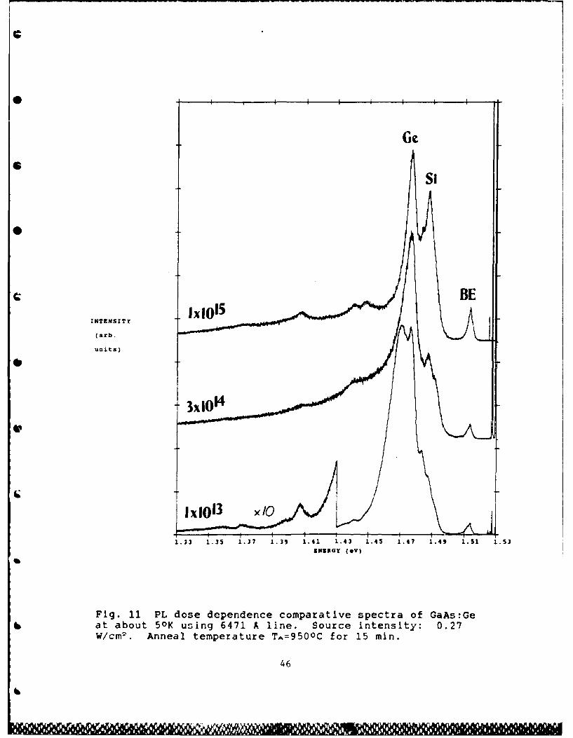
Fig. 11 PL dose dependence comparative spectra of GaAs:Ge46 at about 50K using 6471 A line. Source intensity: 0.27
W/cm2. Anneal temperature TA=9500C for 15 min.
46
GG
rNTENS ITY
(arb.xI 5units)B
Si
001
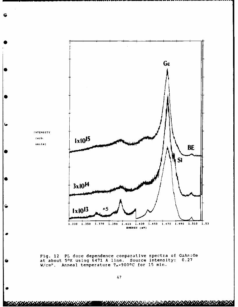
Fig. 12 PL dose dependence comparative spectra of GaAs:Gere at about 50K using 6471 A line. Source intensity: 0.27
W/cm2. Anneal temperature T,.=9000C for 15 min.
47
nu1 n I I - I • -
Si
ttINTINSITY
Sarb. I l l3BEun its)
1,330 1.350 1.370 1.390 1.410 1.430 1.450 1.470 1.490 1.510 1.53
INIIGY (eV)
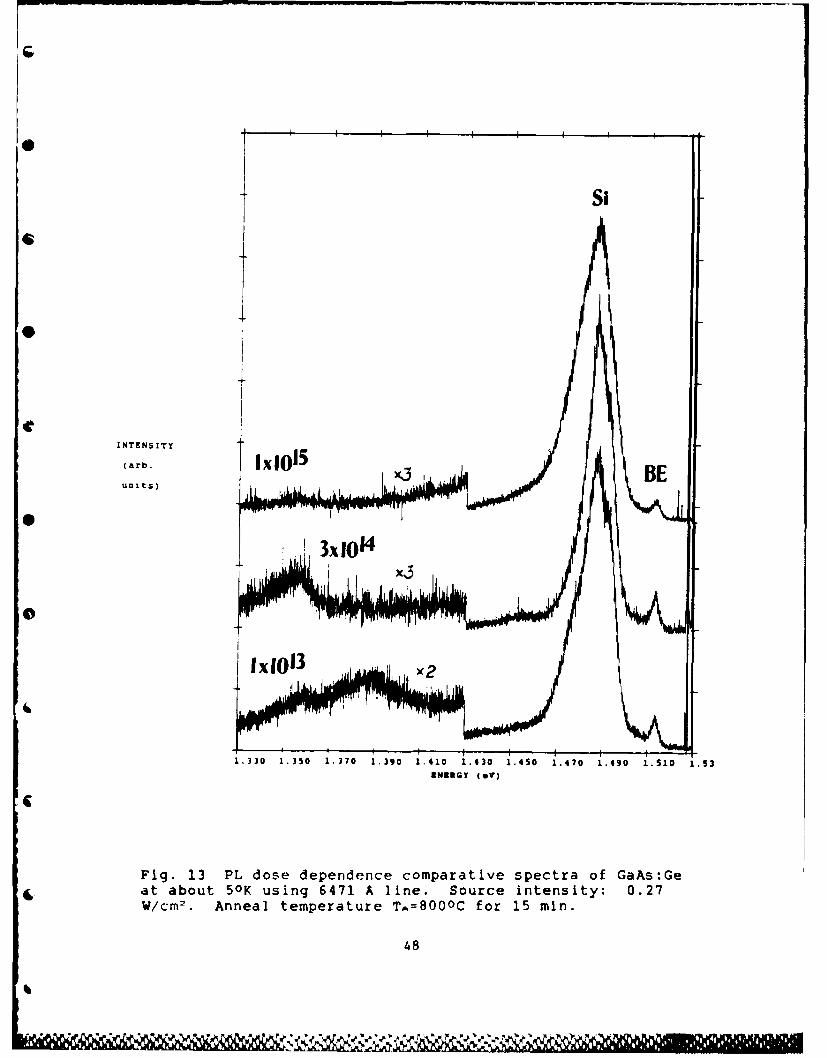
Fig. 13 PL dose dependence comparative spectra of GaAs:Geat about 50 K using 6471 A line. Source intensity: 0.27W/cm7. Anneal temperature T,=800oC for 15 min.
48
Ge
INTENSITY X5I-115B
(arb.
1.330 1.350 14a.37 1 .311.1 1.43 1.i-.7 .40 150 15
ENE*GY (@V)
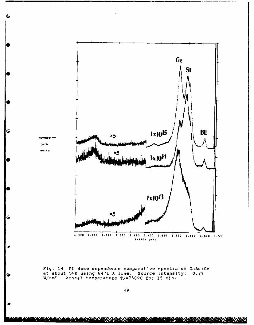
Fig. 14 PL dose dependence comparative spectra of GaAs:Geat about 50K using 6471 A line. Source intensity: 0.27WC'crn. Anneal temperature T.=75OOC for 15 min.
49
Ge
* Si
C
INTENSITY
(arb. 5105
units) BE
ENERGY C@V)
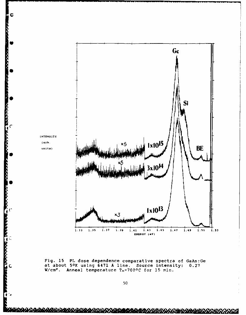
Fig. 15 PL dose dependence comparative spectra of GaAs:Gec. at about 50K using 6471 A line. Source intensity: 0.27
W/cm2 . Anneal temperature TA=7 0 0 0C for 15 min.
so
I Si
95010CBE
INTCNSITY
(arb.
80000* 750CC
1.330 1. 350 1 370 1390 1.410 1.430 1. 450 14 70 1.490 1.510 1.530
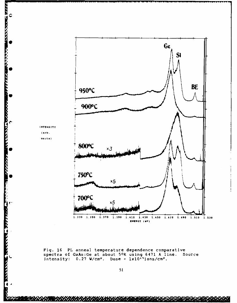
Fig. 16 PL anneal temperature dependence comparativespectra of GaAs:Ge at about 50 K using 6471 A line. SourceIntensity: 0.27 W/cm2 . Dose =lxlO'lons/cm'.
51
Ge
Si
* - 9500C B
(4rb
un its) 8(0 0 1C
7500C
10 )0 10 1Jeo 10 1 10 1 %0 1 470 1 490 1 510 5 53eNtAGY (OV)
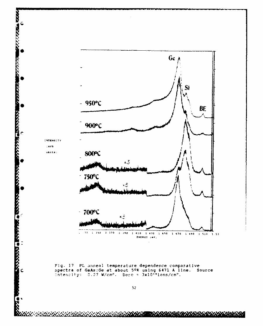
Fig. 17 PL anineal temperature dependence comparativeC spectra of GaAs:Ge at about 50K using 6471 A line. Source
It e rity .2 y/r Dovec 3x10' 4 ions/cmI.
52
CG
SI
*950 0C X/Q N BE
tHTENSITY
Carb.
Suni ts) X3
S7500C
-7000CI \
1.330 1 350 1.370 1. 390 1.410 1.430 1.450 1 470 1.490 1.510 1.53
CNERGY eOV)
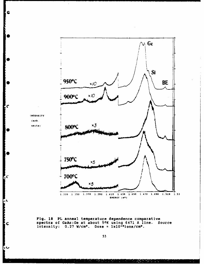
Fig. 18 PL anneal temperature dependence comparativec spectra of GaAs:Ge at about 50K( using 6471 A line. Source
intensity: 0.27 V/cm2. Dose = lxlO12 ions/cm2 .
53
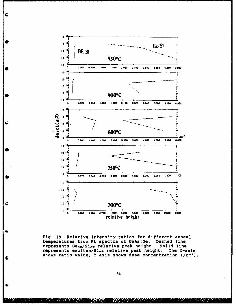
10 24L
,,.. BE Si ....10 --- G--S
o 950c -
100. 0.300 070 1.000 1.440 1.800 2.160 2.520 2.80 3.240 3.600
10 , /10
101 900PC10 l ,,
0. O 0.84 I.no I.M 2.100 80 L940 & O &.M 4MO
10
0. 0.600 1200O 1.600 2.400 3.000 5.6100 .200 4.600 3.400 61.000
1 0 -k "i
ii - -----------
10
10Z0.
0. 0.170 0340 0.510 0.60 0.60 1.020 1.100 1.380 1.30 1.70010
10 14E - ---- - ----------
,o,4 / o c10 11I e ,
0. 0.160 0.10 0.70 1.040 1.300 1.020 1.620 2.060 2340 2.00
relative hc-ight
S
Fig. 19 Relative intensity ratios for different annealtemperatures from PL spectra of GaAs:Ge. Dashed linerepresents GeAS/SiA. relative peak height. Solid linerepresents exciton/Si.. relative peak height. The X-axisshows ratio value, Y-axis shows dose concentration C/cm2 ).
54
' ++g~ |Ignllll l'i I W " ' '" "!++"' ' ' r' 's '10 '
to . .
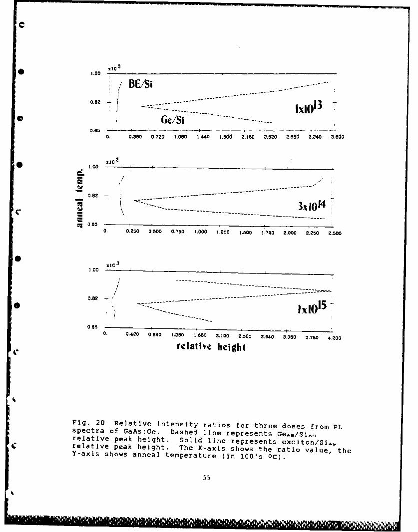
* ~1.00 ~o ES
0.85 Ge/Si
0. 0.360 0.720 1.080 1.440 1.800 2.160 2.520 2.880 3.240 3.600
*1.00 10
0.82
-------------------------------------
0.65-
0. 0.250 0.500 0.750 1.000 1.250 1.500 1.750 2.000 2.250 2.500
1.00 c
----- ----------------------- ----- ------------0.82-
* -* lIO'05
0.650. 0.420 0.840 1.260 1.680 2.100 2.520 2.940 31.360 3 .760 4.200
relative height
Fig. 20 Relative intensity ratios for three doses from PLspectra of GaAs:Ge. Dashed line represents GeAa/SIAYrelative peak height. Solid line represents exciton/Si,,relative peak height. The X-axis shows the ratio value, theY-axis shows anneal temperature (in 100's OC).
55
dependence is clearest as shown in Figs. 11 and 19. The
relative height of the GeAs peak decreases while the relative
height of the exciton peak increases as the dose increases.
As mentioned previously, relative height refers to a
comparison ratio with the Si. peak. The PL data seems to
indicate that an increasing number of Ge atoms are being
located on Ga sites with an increasing dose concentration at
this high anneal temperature. Electrically, a type conversion0
occured between doses of ix10 1 3 and 3xl01 4/cm 2 according to
the electrical study mentioned in chapter III (5).
The dose dependence trend for lower anneal temperatures
isn't as clear. At anneal temperatures 5 8000C the relative
height of the exciton peak is increasing up to a dose of
3x10 1 4/cm 2 and then decreases at 1xl0 15 /cm 2 . At 900 0 C the0
relative height of the exciton peak seems to increase, but the
conclusion is not obvious because the SiM. peak is obscured by
a large Ge.s peak. At 8000C the GeAS peak is obscured by a0
large Si~w peak. The relative height of the GeAs peak at
anneal temperatures at or between 750 and 9000C show a
decrease in size at a dose of 3x10 1 4 /cm 2 and then an increase
in size at 1x101 5 /cm 2 -
In Fig. 20 we can see a complicated behavior in the
anneal temperature dependence of the both the GeM. peak and
the exciton peak. At all dose concentrations, the relative
height of the GeM. peak decreases between 700 and 8000C, and
then increases again. This increase continues up to 9500C for
a dose concentration of ixl01 and 3x101 4/cm 2 , whereas for a
56
dose of ixl0l"/cm 2, the increase continues to 9000C and then
makes a sharp decline at 9500C. The relative height of the
exciton peak shows an increase between 900 and 9500C for all
doses. An overall increase in the relative height of the
* exciton peak with increasing anneal temperature is observed
for both lxlO'3 and ixl0l"/cm2 . This suggests a trend of
increasing donor activity with increasing anneal temperature.
* In the electrical data, the Ge implanted samples showed
n-type behavior at all anneal temperatures for a dose of
Ix10 1 5 /cm 2 , and also at an anneal temperature of 9500C and a
dose of 3xl0'4 /cm 2 . The activation efficiencies for these
samples were low, apparently due to an electrical compensating
effect that occurred between Ge donors and Ge acceptors. The
• PL trends that correlate best with electrical data are those
at high anneal temperatures where p-type activation was the
highest for low doses, and n-type activation was highest at
*the high doses.
It is also noted that for the samples annealed at higher
temperatures of 900 and 9500C, and having higher doses of
3x10"4 and Ixl01'/cm 2 , a high luminescent background is
detected at energies below the GeM. peak. Also, the Ga.
antisite defect is observed, and the 1.406-1.408 eV DAP peak
becomes apparant.
At lower anneal temperatures, the Ga vacancy related
transition at 1.356-1.359 eV is observed and disappears at
higher temperatures.
57
D. Ge+As rmplanted GaAs
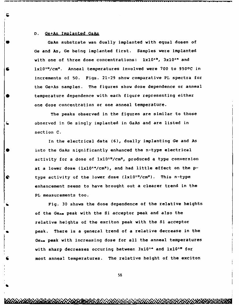
* GaAs substrate was dually implanted with equal doses of
Ge and As, Ge being implanted first. Samples were implanted
with one of three dose concentrations: 1x101 1, 3x10 1 4 and
* 1x101 5/cm 2 . Anneal temperatures involved were 700 to 950 0 C in
increments of 50. Figs. 21-29 show comparative PL spectra for
the Ge+As samples. The figures show dose dependence or anneal
* temperature dependence with each figure representing either
one dose concentration or one anneal temperature.
The peaks observed in the figures are similar to those
observed in Ge singly implanted in GaAs and are listed in
section C.
In the electrical data (6), dually implanting Ge and As
• into the GaAs significantly enhanced the n-type electrical
activity for a dose of 1x10¹¹/cm2 , produced a type conversion
at a lower dose (1xl0 14/cm2 ), and had little effect on the p-
type activity of the lower dose (lxlOIO/cm 2 ). This n-type
enhancement seems to have brought out a clearer trend in the
PL measurements too.
Fig. 30 shows the dose dependence of the relative heights
of the Ge.. peak with the Si acceptor peak and also the
relative heights of the exciton peak with the Si acceptor
* peak. There is a general trend of a relative decrease in the
GeA. peak with Increasing dose for all the anneal temperatures
with sharp decreases occuring between 3x10 4 and lxlO' g for
most anneal temperatures. The relative height of the exciton
58
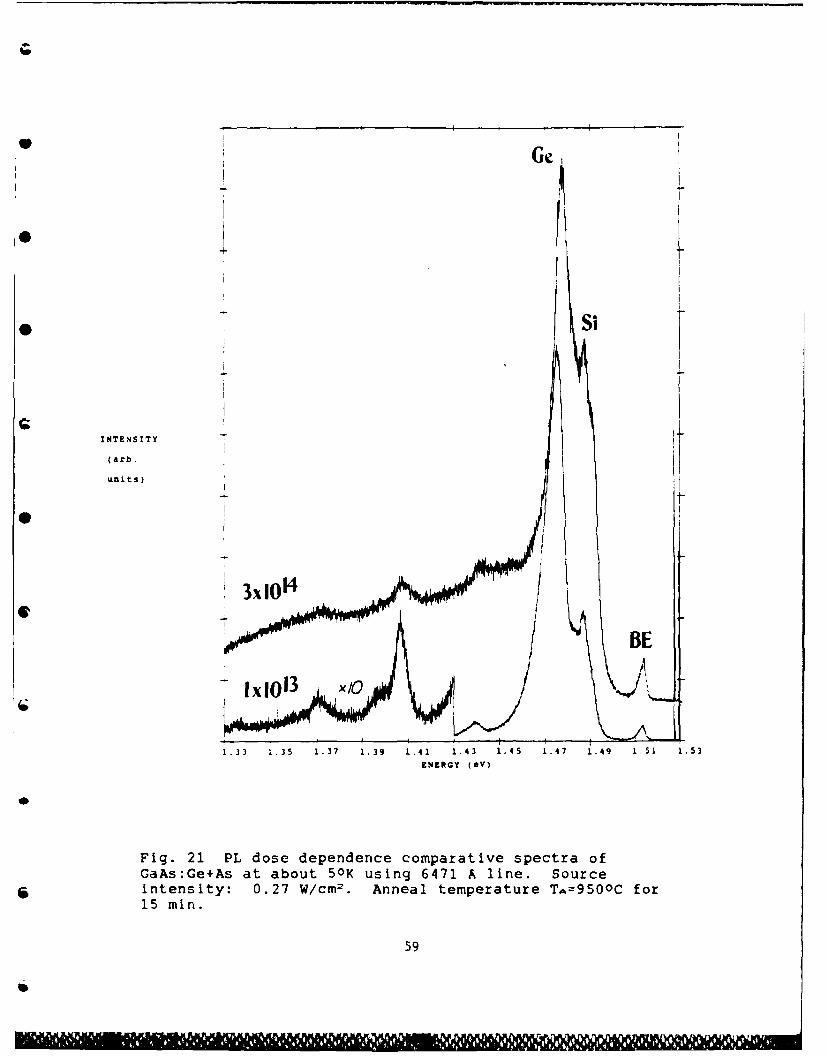
I Ge
* Si
INTENSITY
(arb. t
BE
1.33 1.35 1.37 1.39 1.41 1.43 1.45 1.47 1.49 1.51 1.53
ENERGY (OY)
Fig. 21 PL dose dependence comparative spectra ofGaAs:Ge+As at about 50 K using 6471 A line. Sourceintensity: 0.27 W/cm2 . Anneal temperature TA=9500C for15 min.
59
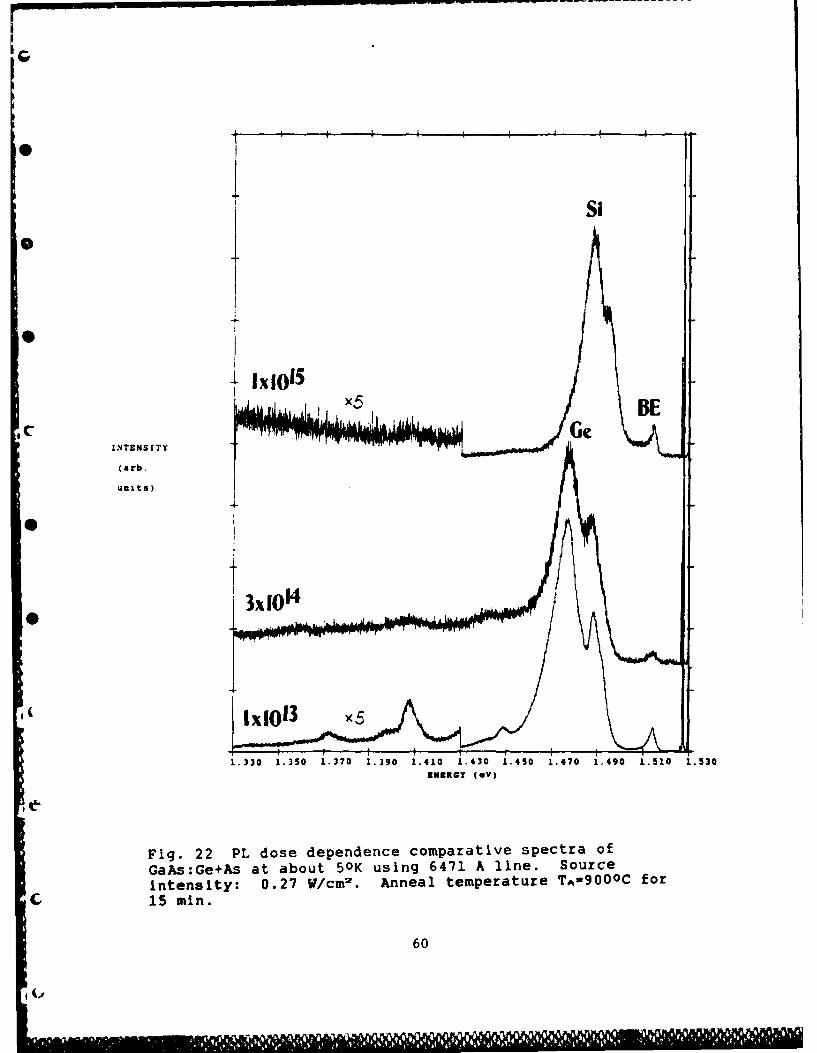
0 Si
1 1,%10 15
i~x 1 .. ,IBEINTENSITY
(arb.
un its)
3%01
13 30 1 .350 1.310 1.390 1.410 1.430 1.450 1.470 1.490 1.510 i.530RNROY (Oy)
Fig. 22 PL dose dependence comparative spectra ofGaAs:Ge+As at about 50K using 6471 A line. Sourceintensity: 0.27 V/cm2. Anneal temperature TA=9000 C for15 min.
60
C 11 1 (A11j l l i m
Si
G,
INTENSITY-
(arb
units)
3.1 1
) 1.330 1.350~ ~~~~A -AA7 1.39 1 .41 . 4 0 . 50 . 70 1 4 0 1 1O . 3INRG (gV)
1aG . at0 abu 35 0 K un 67 .9 .1 .3 O1471 A line Source 5
intensity: 0.27 W/crn2 . Anneal temperature TA=8500 C for15 min.
61
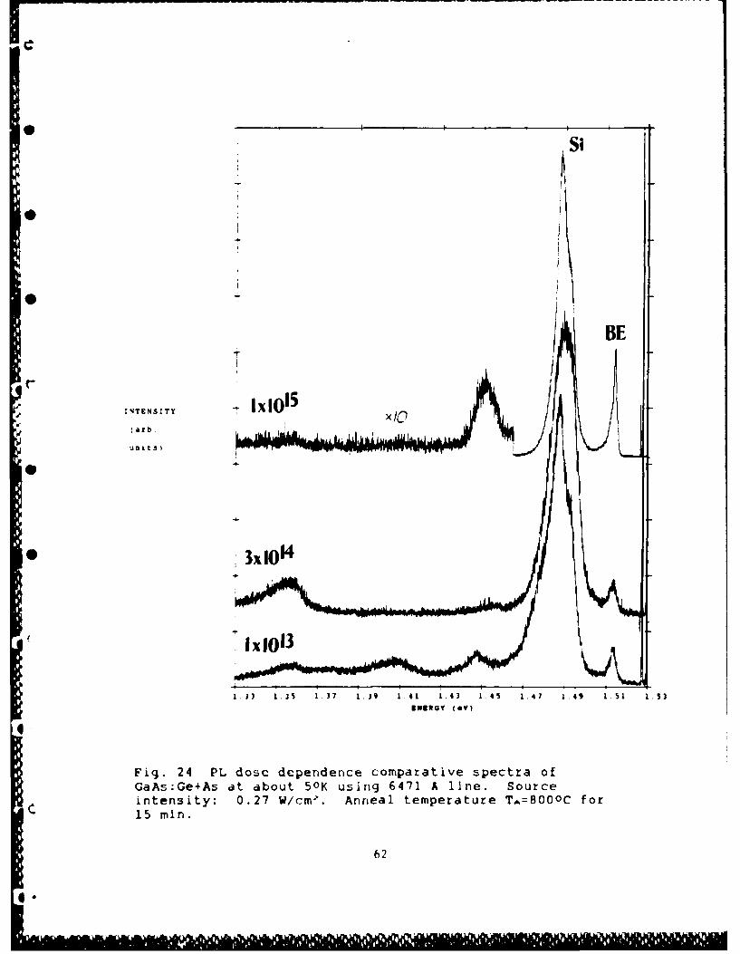
Si
/ BE
INTENSITY I I 1
f arb
3%01
1,J] 1.35 1.37 3.39 1.41 1.43 1.45 1.47 1.49 1.51 1.53ENERGY (V
Fig. 24 PL dose dependence comparative spectra ofGaAs:Ge+As at about 50K using 6471 A line. Sourceintensity: 0.27 W/cm?. Anneal temperature TA=80O0C for
C 15 min.
62
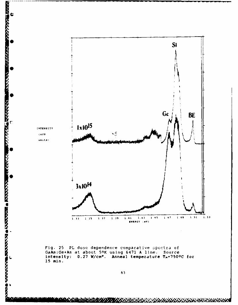
C;
Si
+
tGe BE
TE SIT I,
3%1014
Is1 1 1 37 1 ,19 1 .41 1 4 ) 1 45 1 47 1,49 1 51 1 53
gM33GY (OV)
Fig. 25 PL dose dependence comparative opcctra ofGaAs:Ge+As at about 50 K using 6471 A line. SourceIntensity: 0.27 W/cm2 . Anneal temperature T'=7500C for
15 min.
63
@11
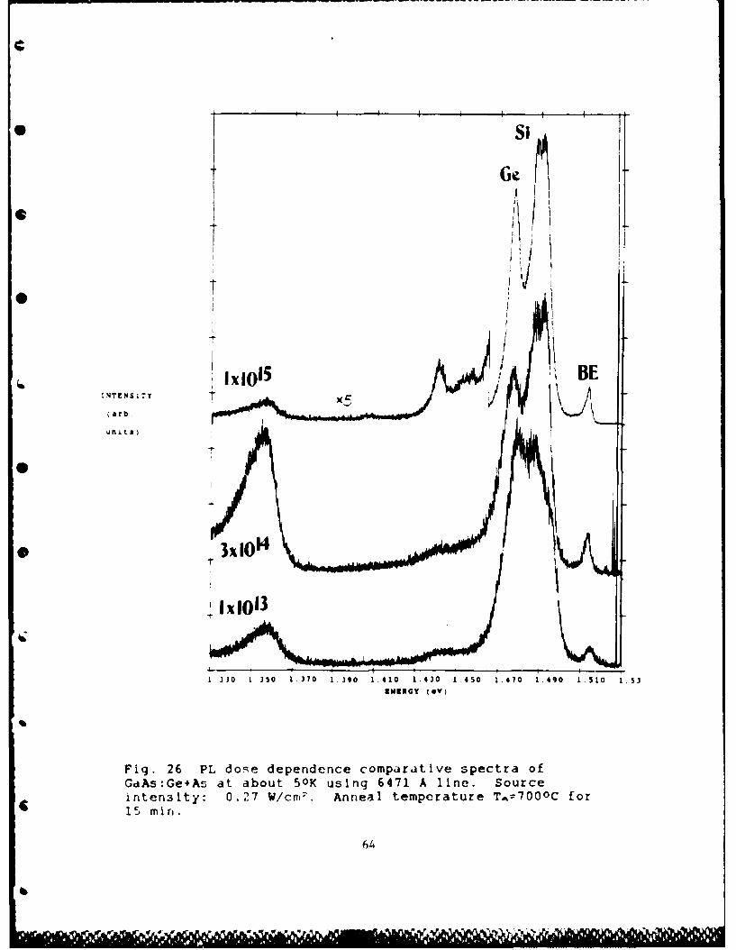
C7
I I I i
C arb
13j30 1 350 13170 1.390 1.410 1.430 1.450 1.470 1.490 1,510 1.53ENOGY (OV)
Fig. 26 PL dose dependence comparative spectra ofGdAs:Ge+As at about 50K using 6471 A line. Source
inltensity: 0.27 W/crn'-. Anneal temperature T^=70OOC for15 min.
64
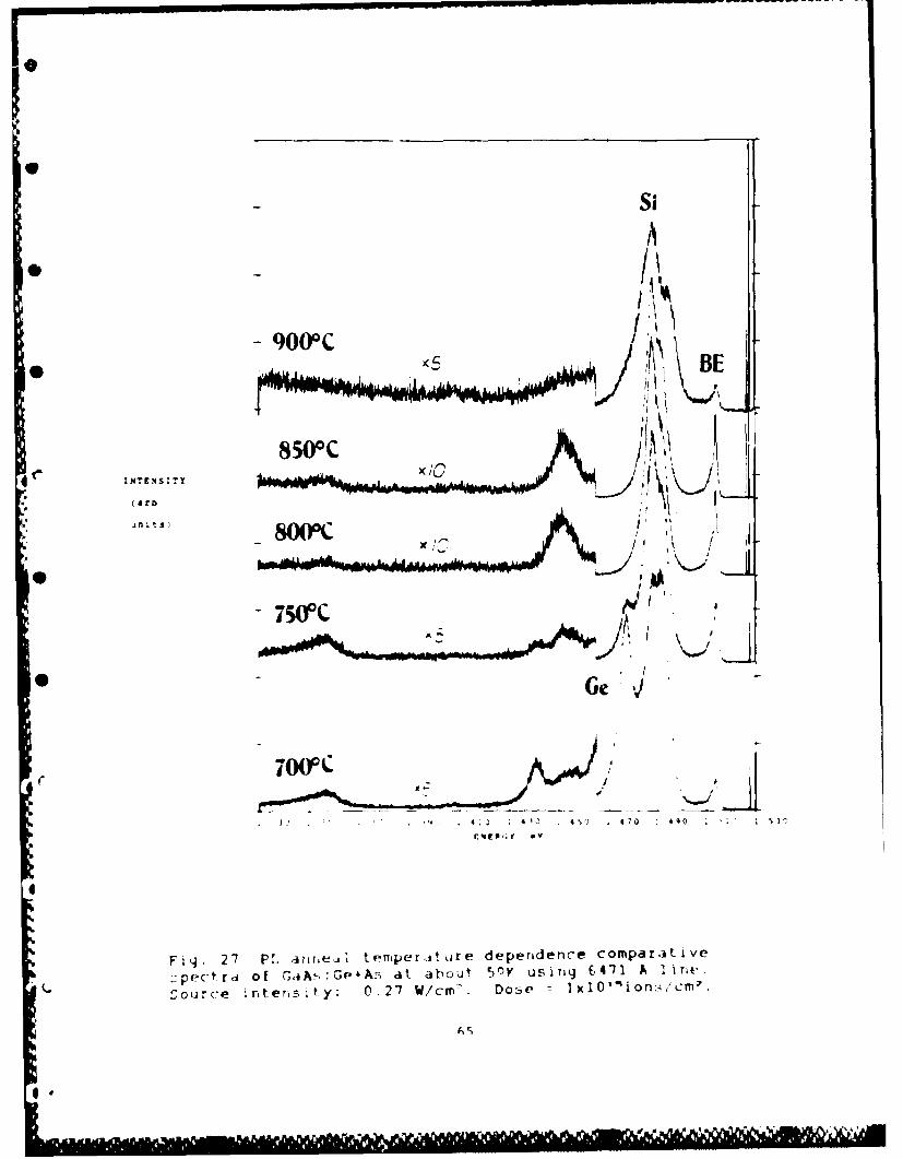
Si
I A
050
INflTE SIT (a:b
*nt3
* Ge8001C
c70; e 40 t0SI
Fig 27 p. f, eA tenmper~iture depenidence comparat~ive:-peclira of (,aA-,: Ge*A~i at about 50Y us ing 6471 A 'A ncv.
o u r cp i rt er y: 0O.27 U/cm7 . Dose xOin:/c-
mmjL.~~~~ -A&Ajj ".-%dlij
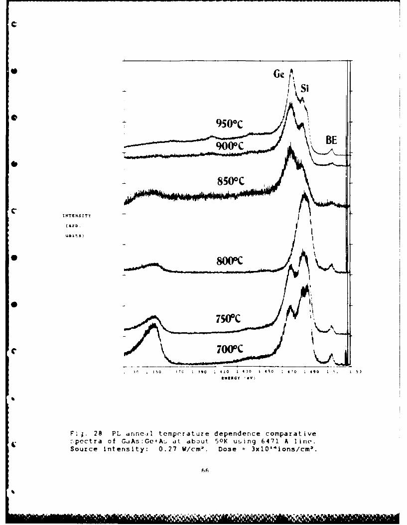
959O
000
INTENSITY
(arb.
units)
7500
3n )so~ )7 0 )9 0 1 4 0 1 4 0 4 ,0 i 490 1;. i l
F~j 28 Pll arne.,jl tempnrature dependence comparativepectra of GjAs:Ge4AL, at about 50K u!,ing 6471 A linv.
Source Intensity: 0.27 V/cm2 . Dose 3x10'4 lons/cm2 .
66p
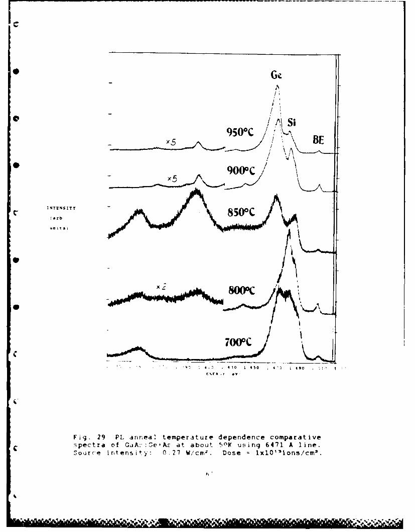
eG
9500C Si B
85-0:&rb
Uf t S)
Sx
C1
14 4, a 4)0 1 4SO 4n,0 'i ,
E1%FP Y *V
Fig. 29 P1. anneal temperature dependence comparativespectra of GaA-: :Ze4Az at about 50YK using 6471 A line.Source intensity: 0.27 W,'cm,?. Dose -lxlO'"lons/cn 2 .
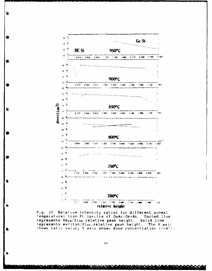
* 0,- G 1SI0
!0 BE/Si 950"C
0120 0820 0930 10 , 50 1MS 0 270 2460 790 .103
S
Ic----------- ----- -
0:
10~ 900PC __ _
c 0 170 0340 0 517 .38' C0G 1.020 2 190 2360 : 30 .703
10
10
r4 0850 0C7 0 170 0340 0510 346 0850 1.020 1 1OO 1.360 :30 03
20
0 AL
01.... . ._ .,,f __._ ---.--_------ -- -
1100
0 500 000 530: 300 2 500 3000 1500 4000 00 003
IC -
10
c7 70 3 41 50C
Ile 00 7IX 27 0 0600 07?00 c 60o 00 PM 0W
700
Fig. 30 Relative intensity ratios for different anneal1emperaturei frory, Pl. 5pectra of GaAs:Ge+As. Dashed linerepresents GeA/Si.% relative peak height. Solid linerepresents exciton,'Si.,. relative peak height. The X-axi:.;hows ratio value, Y axis show:: dose concentration (c~
peak increases between doses of 3x101 4 and 1xl0'"/cm2 for
anneal temperatures 750-9000C. In the electrical data, the
sharpest increase in sheet carrier concentration and
activation efficiency occured between 3x10 14 and 1xl0 1s/cm 2
for anneal temperatures ! 8500C. The dose dependence suggests
a trend of a decreasing percentage of Ge atoms locating on As
sites with increasing dose, whereas an increasing number of Ge
atoms locating on Ga sites which becomes apparant at the
higher doses.
The anneal temperature dependence (Figs. 27-29) shows
a similar behavior to that of Ge singly implanted in GaAs, in
that the Ge.. peak becomes obscured in a large SIAm peak at an
anneal temperature of 800oC. This gives the trend of relative
Ge,. intensity a characteristic "V" shape as graphed in Fig.
31. This relative Ge,. peak height tends to decrease up to
800oC and then increase again at higher anneal temperatures.
At a dose of lxl0"/cm2, the GeA. peak decreases up until it
has mostly disappeared at an anneal temperature of 8500C, and
then slightly beg is to reappear as part of a broad Si.. at
900 0 C. The exciton mirrors this behavior by increasing in
relative height up to 8500C and then by decreasing at 9000C.
This dose does seem to show an overall trend towards
increasing n-type activity with increasing anneal
temperature. On the other hand, the other two doses show an
overall trend of increasing p-type activity with anneal
temperature.
It is interesting to note that like Ge singly implanted
69
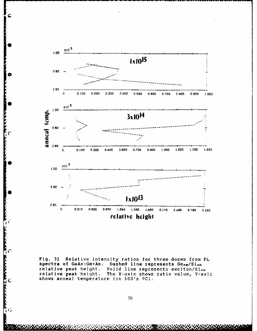
1.00
-------- - - - - - -------- - --- --- - --
0.650 0.100 0200 0.300 0.400 0.500 08600 0.700 0.800 0.900 1.000
. 1.00
------------------ ----------082 -- - - -- - - -- - - -
0. 0.150 0300 0.450 3.800 0.750 0.900 1.050 1.200 1.350 1.503
SIC31.00.
------------ --- -- ------------ -
0.82 -- - -- - -- - -
* --------- --------
085 lxIOl3
0. 0.310 0820 0.930 1.240 1.550 1.880 2.170 2.480 2.790 3.100
relative height
Fig. 31 Relative intensity ratios for three doses from PLspectra of GaAs:Ge+As. Dashed line represents GeAs/SiAGrelative peak height. Solid line represents exciton/SiA&relative peak height. The X-axis shows ratio value, Y-axisshows anneal temperature (in 100's OC).
70
1i~~~ .... . . . . . . -.. ...
GaAs, the Va^ defect at 1.356-1.359 eV only appears in samples
* •that were annealed at temperatures s 8500C. The 1.406-1.408
eV DAP peak appears in samples with anneal temperatures ;
8000C for a dose of 1x10¹³/cm, and at temperatures t 9000C
for a dose of 3xl0'4/cm2 , and is not observable for a dose of
1xl0 15 /cm2 . For an anneal temperature of 8500C and a dose of
1x10 1 3/cm 2 , the 1.406 eV peak is the most significant peak in
* the PL spectrum.
Ge+As Implanted GaAs, like Ge implanted GaAs, sometimes
shows a high relative background emission at energies below
the GeAe peak. This occured at 850-9500C for a dose of
3x10 14/cm 2 , and 850 0C for a dose of Ix101 3 /cm2 .
E. Ge+Ga Implanted GaAs
For these samples, Ge and Ga were implanted sequentually
into GaAs substrate. The dose concentrations were ixl01 3 ,
1x10 1 4 , 3x10' 4 , and lxlO'5 /cm2 . Only two anneal temperatures
were studied, 900 and 9500C. The peaks observed were again
similar to those seen in Ge singly implanted GaAs, with two
exceptions: a) A resolved exciton peak at 1.512 eV shows up at
an anneal temperature of 9500C and a dose of lxlO 3 /cm2 .
According to Heim and Hiesinger (15:464) this peak fits the
assignment of an exciton bound to a neutral acceptor. b) A
peak at approximately 1.239 eV was observed at a dose of
3x10 14 /cm2 and an anneal temperature of 9500C (it is not shown
In the figure). This seems to be the same peak that has been
,tserved at 1.283 eV by Shanabrook et. al., and they
71
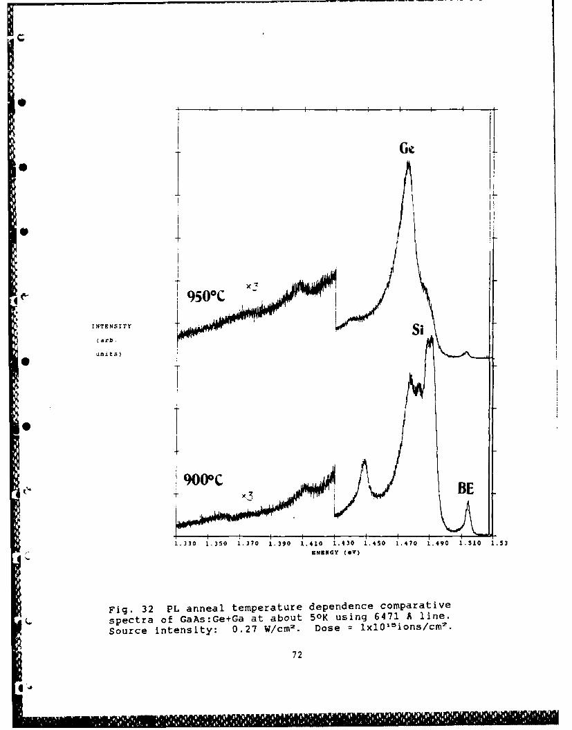
Ge
0x
9510
INTENSITY S(arb.
units)
+9000C BE
1.330 1.350 1.370 1.390 1.410 1.430 1.450 1.470 1.490 1.510 1.53
ENERGY (OT)
Fig. 32 PL anneal temperature dependence comparativespectra of GaAs:Ge+Ga at about 50K using 6471 A line.
Source intensity: 0.27 W/cm2.- Dose = lXlO15Jions/cm2.
72
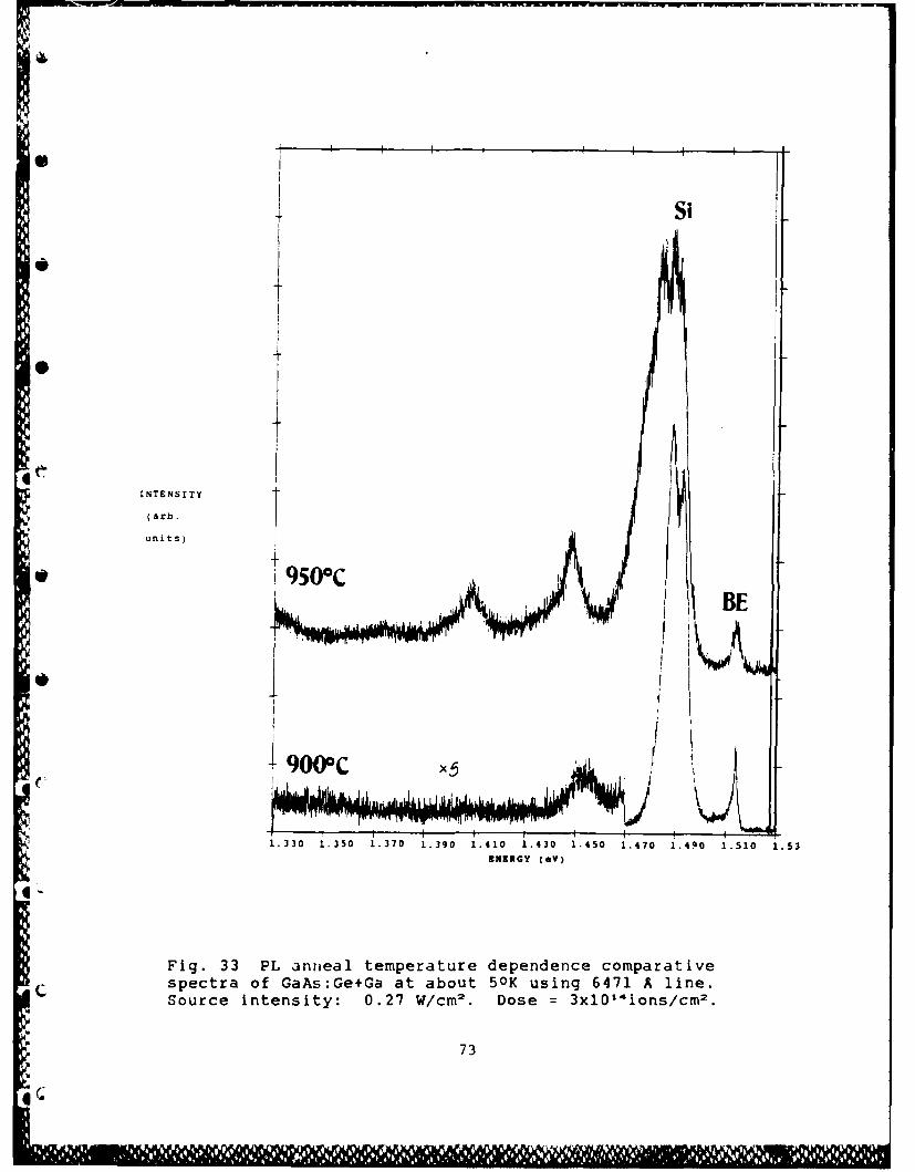
T Si
INTENSITY
) (arb.
units)
BE
1. 330 1. 350 1. 370 1. 390 1.410 1.430 1.450 1.470 1.490 1 510 1.53ENERGY (eV)
Fig. 33 PL anneal temperature dependence comparative
spectra of GaAs:Ge+Ga at about 50K using 6471 A line.Source intensity: 0.27 W/cni2 . Dose =3xl1 4i1ons/cm 2 .
73
"MMI
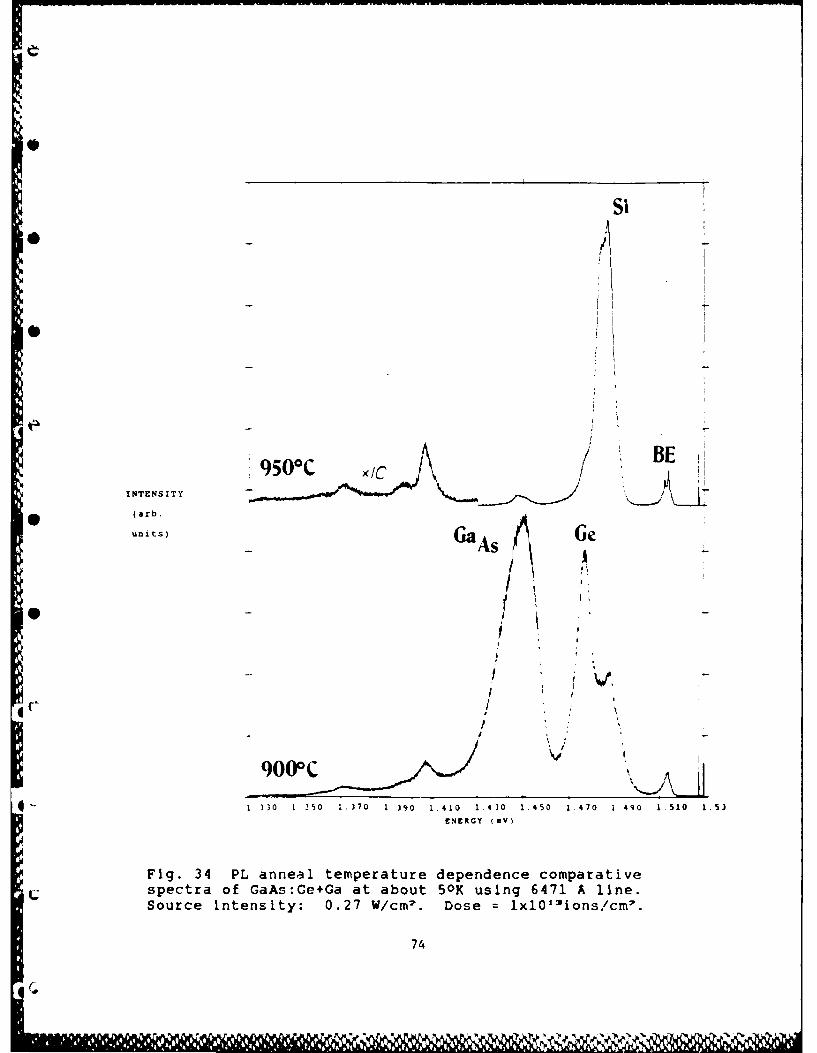
Si
* I'
eF
95010C xCB
I NTENS ITY .,S4P
* (arb.
units) GaAs Ge
jt
'
E
I
a
I
9000C V
1,330 1 250 1.370 1 390 1.410 1.430 1.450 1.470 1 490 1.510 1,53
ENERGY (eV)
Fig. 34 PL anneal temperature dependence comparativespectra of GaAs:Ce+Ga at about 50K using 6471 A line.Source intensity: 0.27 W/cm?. Dose = lxl01ions/cm'.
74
C
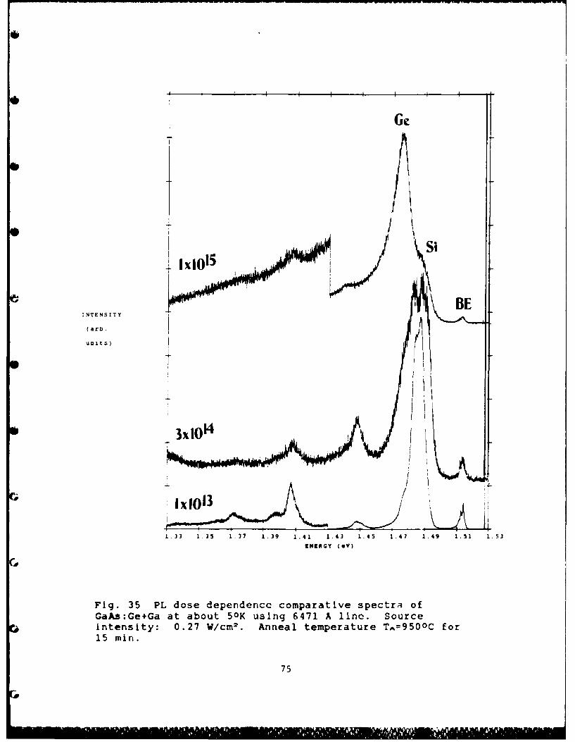
I I I Ge
Si
BEINTENSITY
(arb.
units)t
3xION4
1.3 13 .7 1.39 1.41 1.43 1.45 1.47 1.49 1.51 1.53ENERGY COY)
C,
Fig. 35 PL dose dependence comparative spectra ofGaAs:Ge+Ga at about 50K using 6471 A line. Sourceintensity: 0.27 W/cm2. Anneal temperature TA=9500 C for15 mini.
75
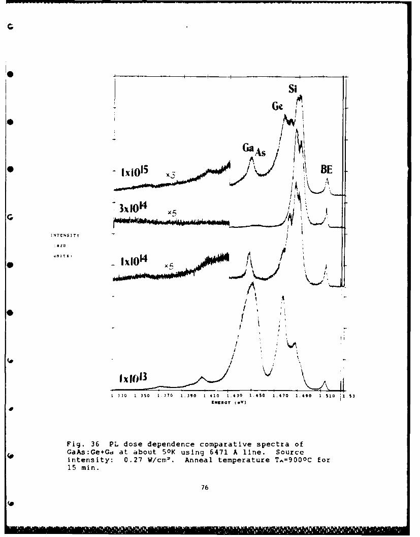
Si
+ Ga As
I~ ~ ~ ~ XA0 7B
3x10¹⁴
:NTENSITY -
arb
in I t A I/L t
jxjO14
1 3)0 1 350 1.370 1390 1 410 1.430 1.450 1.470 1.490 1.510 1.S3
IERCGY (OV)
Fig. 36 PL dose dependence comparative spectra ofGaAs:Ge+Gd at about SOK using 6471 A line. Sourceintensity: 0.27 W/CM2 . Anneal temperature T^=90OOC for15 min.
76
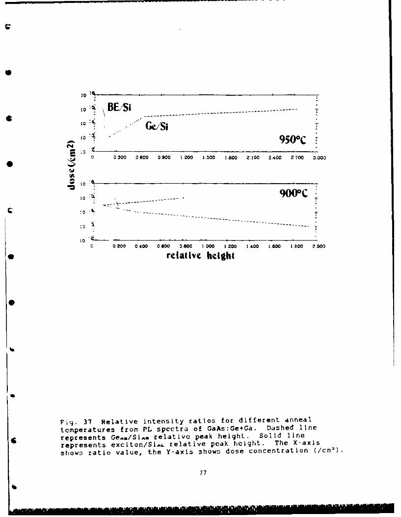
10
C 10 4, 'S
~ - G&SiC~d 950 0C
0 0.300 0600 0.900 1.200 2.500 1.800 Z.100 2,400 2700 3.000
0 ----------------------------------------- .-------------------
10-- - - - - - -
10:;0 0200 0400 0600 3,800 1000O 1200 1.400 1.600 100o 2000
* rcInv hclght
Fig. 37 Relative intensity ratios for different anneal
temperatures from PL spectra of GaAs:Ge+Ga. Diished line
*represents Ge~f/Si~o relative peak height. Solid line
represents exciton/SI,. relative peak height. The X-axis
shows ratio value, the Y-axis shows dose concentration (/cm').
77
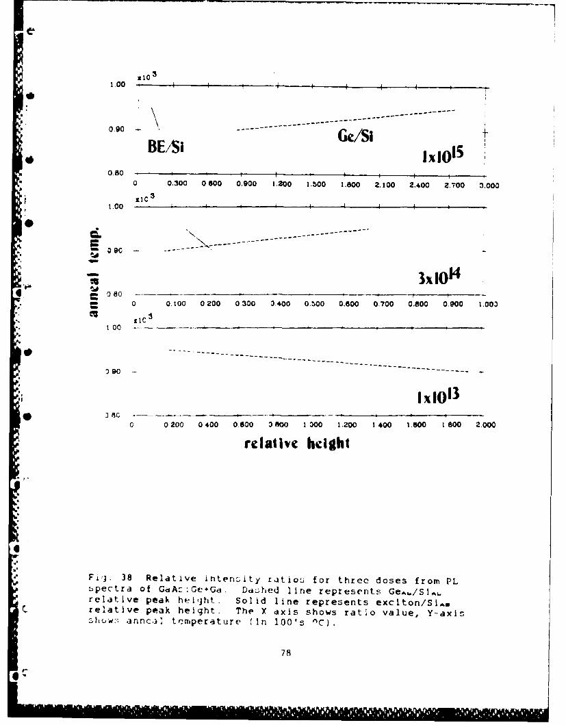
ztC3
1.00 , .
0.90 -- - - - - - - - -
BESGe/Si
0.80 , I-. . I ,,0 0.300 0 800 0.900 1.200 1.500 1.800 2.100 2.400 2.700 3.000
100 lC3 I~~~~~~1.00 , , i€ _ _
-----..-------------------0 0
0 0.100 020 00300 0.400 0.500 0.600 0.700 0.800 0.900 1.000
",. tic1 00
~9 - - - ---- -----------------------------------------------I IxlOI13
0 0200 0400 0600 06800 1 000 1.200 1400 1600 1800 2000
relative height
*. Fij. 38 Relative intensity rdtio5 for three doses from PLbpectra of GdAz:Gc+Gd. Ddi ,hed line representS, Ge^./Sl,,.relative peak heijht. Solid line represents exciton/SiA.
C. relative peak height. The X axis shows ratio value, Y-axlsowc; annc,3" temperature (In 100's AC).
78
attributed it to a donor-Ga.. double acceptor transition. The
transition leaves the final state of the negatively charged
double acceptor in an excited state (30).
The comparative spectra are presented in Figs. 32-36, and
graphs of relative intensity ratios are presented in Figs. 37
and 38. In observing the anneal temperature dependence
(Figs. 32-34, and Fig. 38), a relative height increase occurs
for the Ge.. peak and a decrease occurs for the exciton peak
between 900 and 9500C for doses of 3x10l* and lxl0'l/cm.
This suggests that Ge atoms are tending to locate more on As
sites than on Ga sites from 900 to 9500C. This is interesting
because in the electrical data, GeAs:Ge+Ga showed a type
conversion from p-type to n-type activity at these high anneal
temperatures. On the other hand, the PL data implies a shift
to stronger p type electrical activity. At lxl0'"/cm " , the
relative height of both the Ger peak and the exciton peak
decreases from 900 to 9500C. This behavior is not yet well
understood.
The trends for dose dependence (Figs. 35,37) are also not
well understood. At an anneal temperAture of 900 0 C, the
relative height of the Ge.. peak decreases with increasing
dose up to 3xl0'4 /cm', at which point it mostly disappears.
The peak returns at a dose of lxlOO/cm*. The relative
height of the exciton peak shows a general decrease with
Increasing dose. At an anneal temperature of 9500C, the trend
shows a relative height increase for the Ge.. peak and a
79
*. .
decrease for the exciton peak with increasing dvse, Implying
an Increase In p-type electrical activity. This is Just
opposite of what one might expect, because in the electrical
data there is a type conversion to n-type activity between
doses of 3xl1' and lxlO"5/cm2 at an anneal temperature of
9500C.
In the electrical data, for GaAs:Ge+Ga, the p-type
activity was enhanced over that of GaAs:Ge for doses of
3xl0'4/cm2 or below, and the original n-type activity of
GaAs:Ge changed to p-type except at 900 0C or above.
The maximum activation efficiency OrCCured at an annealt
temperature of 9500C and a dose of lxlO'",cm~. From the PL
data, it seems that the maior contributor by far to the p-type
activity for this sample is the Si.. peak, riot the Ge,%s peak,
and this is not well understood at presen'
At 9000C and 1x101 3 /cm' an interest irii phienomenon occurs.
* The Ga,. ant isite defect peak at 1.4,n~ cv ho'wr lip as the
dominant peak In the spectrum. Other '-m '*at 9000C anneal,
lxin-' and lxl0l"/cm2 dose (Fig. 36), arid ore at 4500C anneal,
*3x10'/cml dose (Fig. 3'1, show relat iv# ., ir it Ga.. peaks
also. The implantation of Ga into the samp~p!5 qeneral'ly
increases the probability of this defet );-jrrinq. This
defect, which acts as a double acceptor, may orit r Ibute to the
p-type electrical activity.
F. Ia 1 cisCniaio
- As a final comparisors, several samples with Identical
anneal temperatures and dose concentrations but different ion
80
species combinations were measured optically and plotted
* together. The different combinations of ion species include
Ge singly, Ge+As dually, GetGa dually, Ga singly, and As
singly Implanted into GaAs. The data for Ga singly and As
6 singly implanted at doses of lxlO' 3 and 1xl01 8 /cm2 and an
anneal temperature of 9000C, was provided by Capt. K. Keefer.
The comparative spectra are shown in Figs. 39-44.
* Figs. 39-41 show how dually implanting Ge and Ga enhance
the Ga.e antisite defect peak. In Fig. 42, implanting As
enhances the 1.357 eV Ga vacancy related transition. Any
trends dealing with the ion species dependence of the Ge.
peak and the exciton peak are not apparant. In Figs. 43 and
44, dually implanting Ge+Ga and annealing at 9500 C greatly
* enhance the SiM. peak relative to the Ge. peak, whereas Ge+As
dual implantion seems to only slightly reduce the Ge.. peak
relative to the Si . peak. However, for a dose of lxl0'l/cm2
* and an anneal temperature of 9000C (Fig. 39), dually
implanting Ge+As qreatly reduces the relative height of the
Ge,.o peak.
81
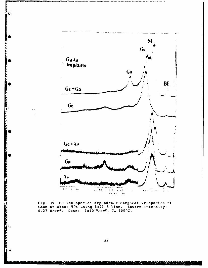
Si
implantsGa '
A
G~~Galaws'BE
Ge +As
(.A
)00 4. a a
Fig. 39 PL ion species dependence comnparative spectr4 rtGaAs at about SOK using 6471 A line. Source intensity:0.27 V/cm2 . Dose: 1xlO's/cm', TA%-900OC.
82
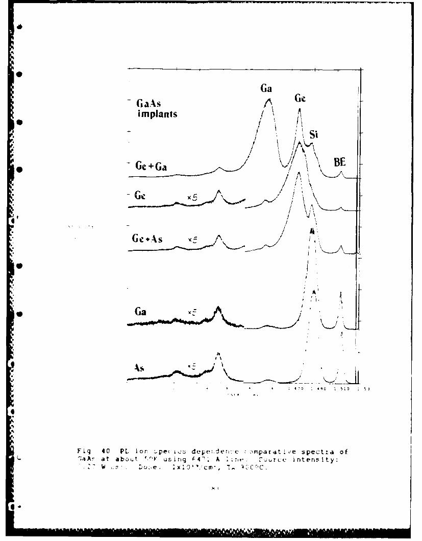
,
Ga
implants ASi
/ B
- Ge+Ga BE
I A
i-
BE
A \G+
Gc a
A /I'/
II'
F g 40 PL or', pec ic de ve:der-c mpardt.i'e spectra of
a T A ! a t a b out, i r i . 4' A i t . f r c L i n t e n s i t y :
. . ,e .C
-. c
l
eII
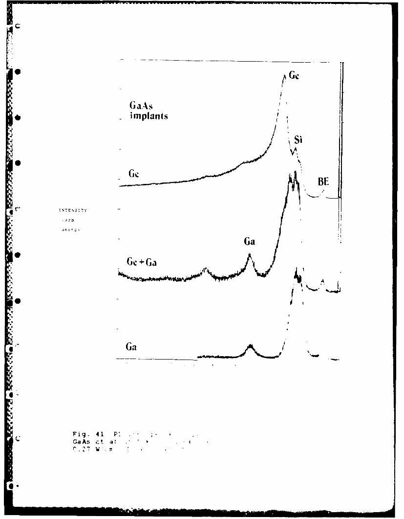
- . Ga-As/i
ICI
G-AS/ .implants
I Si
"e BE
NTENSTy-
In 1r
Ga
Ge+Ga
,,
Ga Now
Fig. 41 P' ,;
C" ~ 41Ga A s c t a., 4r . 2 W rr
rO -A89 688 OPTICAL. STUDY OF GERMN~IUM GERMNIUM PLUS ASENIC
AND 212GERMNIUM PLUS GALL (U) RIR FORCE JUST OF TECHURIGMT-PATTERSON AFS ON SCHOOL OF ENGI T G ALLEY
UNCLASIFE DEC 87 AFIT/GEP/ENP/87D-i F/G 28112 U
I~Wo
.. IWA OCOPY RESOLUTION TEST 'CHART
0iil
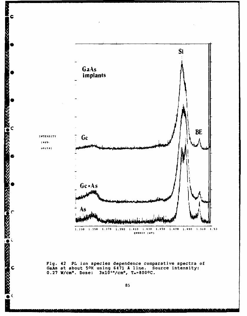
Si
GaAsimplants
C BE
(arb.
units)
10 o
1. 230 1. 350 1.370 1. 390 1.410 1,430 1.450 1 .470 1. 490 1.510 1. 53ENERCY (eV)
Fig. 42 PL ion species dependence comparative spectra ofC GaAs at about 50K using 6471 A line. Source Intensity:
0.27 V/cm2 . Dose: 3x10'14/CM2 , TA=8000C.
85
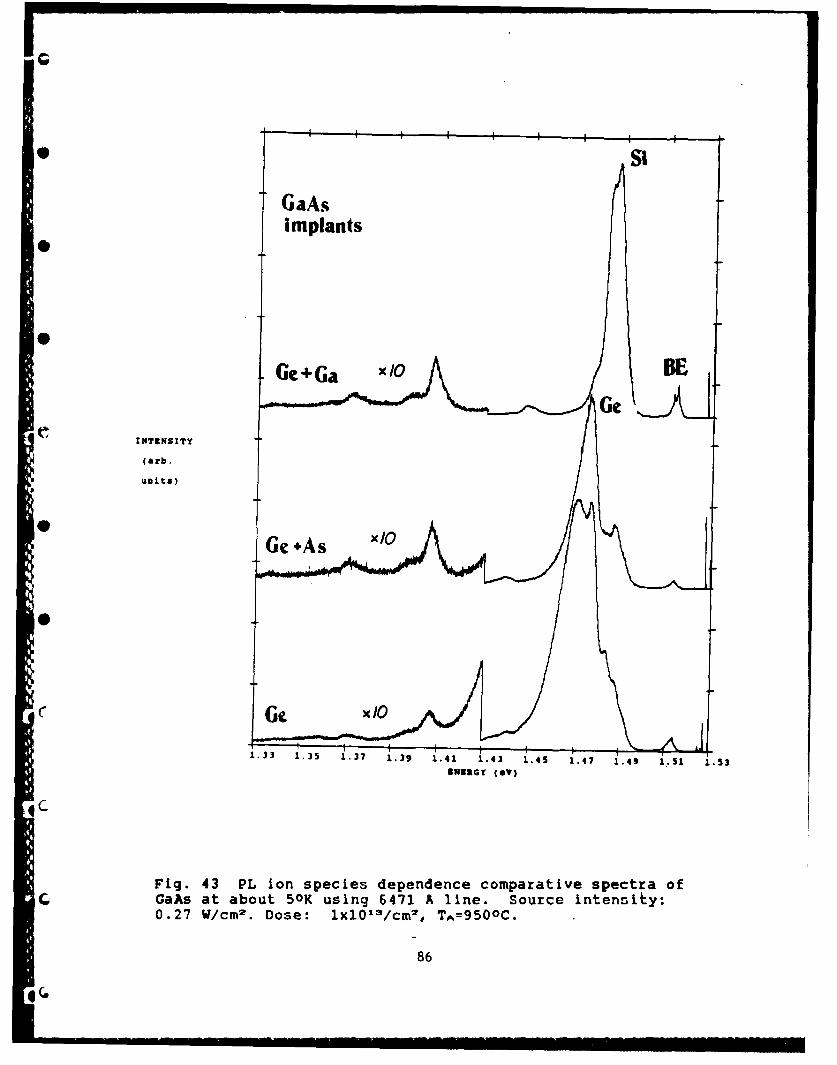
* SI
GaAsimplants
0
G +Ga x /0EG
eINTRNSITY
(arb.
units)
Gc x/O
1.33 1.35 1.37 1.39 1.41 1.43 1.45 1.47 1.49 1.51 1.53
SNERGY (OV)
IC
Fig. 43 PL ion species dependence comparative spectra ofC GaAs at about 50K using 6471 A line. Source intensity:
0.27 W/cm 2 . Dose: ixl0'3/cm2 , TA=950oC.
86
*c:
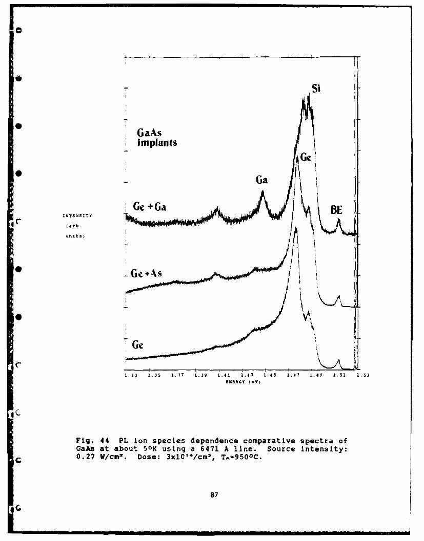
S1
GaAsimplants Ge
GGa
G- Ga.a.BEINTENSITY
(arb.
units)
• - Ge +,As
-G/
1.33 1.35 1.37 1.39 1.41 1.43 1.45 1.47 1.49 1.51 1.53
ENERGY (*V)
IC
Fig. 44 PL ion species dependence comparative spectra ofGaAs at about 50 K using a 6471 A line. Source intensity:0.27 W/cm2 . Dose: 3x10¹⁴ /cm2, TA=9500 C.
87
CG
V. Conclusions and Recommendations
A. C
In the past chapter, the comparative PL spectra was
reviewed for Ge, Ge+As, and Ge+Ga implanted GaAs, some of
which was compared to electrical data from previous studies
as discussed in chapter III. Much of the PL data does not
directly correlate with the electrical data. An effort was
made to use the height of the Ge~e acceptor peak relative to
the (e,SiAo) peak as an indicator of p-type activation and to
use the height of the donor bound exciton peak as an
indicator of n-type activation.
It seems that when the n-type electrical activity is the
greatest in a group of samples, the PL trend becomes more
apparant, and when the n-type activity is reduced, the PL
trend is more obscure. This is substantiated by the fact that
dual implantation of Ge and As showed trends that more closely
matched the results of the electrical data, while the dual
implantation of Ge and Ga showed the least clear trends.
The PL data for Ge+As dually implanted GaAs showed an
overall dose dependent trend of a decreasing percentage of Ge
atoms locating on As sites with increasing dose. It also
showed an increasing number of Ge atoms locating on Ga sites,
which is more apparent at higher doses. An anneal temperature
dependent trend at a dose of lxlO'M/cm2 indicated an overall
tendency towards more n-type activation with increasing
anneal temperature. However, other doses were less clear.
88
For Ge singly implanted GaAs, a clear trend in dose
* dependence, matching the electrical data, occurs at an anneal
temperature of 9500C. The relative height of the GeM. peak
decreases while the exciton peak increases, indicating a
* tendency towards greater n-type behavior. The anneal
temperature dependence for doses of lxl01 and 1x101 a/cm2
showed a general tendency of increasing relative exciton peak
* height with increasing anneal temperature, while the other
dose studied showed an increase in relative exciton peak
height between 900 and 9500C. Although the indicator of p-
type activity, the GeAs peak, didn't show corresponding
behavior, the exciton peak trend suggests an increase in donor
activity with increasing anneal temperature at high ion dose
* concentration.
For Ge and Ga dually implanted GaAs, no definite trend
is observed with the limited number of samples studied.
* However, adding Ga does generally enhance the Ga~n antisite
defect transition that functions as a double acceptor.
B. RecommendationsC
The PL measurements in this study were all done using a
647.1 nm laser line. This line penetrates about 3000 A, well
past the Ge projected range of 464 A, or most of the implanted
region that extends to about 2400 A. Therefore, it is
possible that the Si and C transitions intrinsic to the
substrate are masking the trends in the transitions occuring
in the Implanted layer. The use of a laser line less than
89
I III I . . . I I I . . . ' i -
647.1 nm that does not penetrate the sample as far might have
given clearer results by showing more of what goes on in the
implanted layer only.
I would therefore recommend conducting a study similar to
* this one at a lower laser wavelength. The silicon acceptor
peak may or may not still be a dominant transition.
A study could also be conducted as a function of depth
* into the sample by either etching samples themselves or
varying the laser wavelength.
I would also recommend "filling in the gaps" in this
C study by especially measuring more GaAs:Ge+Ga samples annealed
at lower temperatures than 9000C. It might be useful to study
more dose concentrations such as 3xl10' or lxlO'4/cm2 for all
* species of samples.
9
90
6
Bibi ogaphy
1. Frensley, William R. "Gallium Arsenide Transistors,"BSci...Am., 257(1980),80-87.
*2. Chan, S. S., G. T. Harcyk, B. C. Streetman. "ElectricalProperties and Photoluminescence Studies of Ge-Implanted GaAs," J_ Electron. Mat., 10(1981), 213-238.
3. Ploog, K., A. Fischer, H. Kunzel. "Improved P/NJunctions in Ge doped GaAs Grown by Molecular BeamEpitaxy," App.Ph&, 18(1979), 353-356.
4. Yoder, H. N. "Ohmic Contacts in GaAs," olidS.L
5. Yeo, Y. K., 3. E. Ehret, F. L. Pedrotti, Y. S. Park,C W. H. Theis. "Amphoteric Behavior of Ge Implants In
GaAs," Appl. Phys. Lett., 35(1979), 197-199.
6. Yeo, Y. K., F. L. Pedrotti, Y. S. Park. "Modificationof the Amphoteric Activity of Ge Implants in GaAs byDual Implantation of Ge and As," J. ADpi. Phvs.1, 51(1980), 5785-5788.
7. Pedrotti, F. L., Y'. K. Yeo, 3. E. Ehret, Y. S. Park."Dual Implantation of Ga and Ge into GaAs," J.AplPhs. 51(1980), 5781-5784.
*8. Yu, P. W. "Deep Emission Centers in Ge-Implanted GaAs,"J. Appl. Phvs., 50(1979), 7165-7167.
9. Thoma, Capt Barry P. Photoluminescence Study of GetImplanted GaAs. MS thesis, AFIT/GEP/ENP/86D-11.
( School of Engineering, Air Force Institute ofTechnology (AU), Wright-Patterson AFB OH, Dec. 1986.
10. McKelvey, 3. P. Solid State and Semiconductor Physics.New York: Harper Row Publishers, 1966.
11. Williams, E. W., H. Barry Bebb. "Photoluminescence II:Gallium Arsenide," Semiconductors and Semi-metals. Vol.L edited by R. K. Villardson and A. C. Beer, New York:Academic Press, 1969.
12. Morgan, D. V. et. al. "Prospects for Ion Bombardmentarnd Ion Implantation In GaAs and IriP DeviceFabrication," IRA Proceedincs, 128(1981), 109-130.
91
13. Ambridge, T., and R. Heckingbottom. "Ion Implantationin Compound Semiconductors--An Approach Based on SolidState Theory," Radiat. Eff., 17(1973), 31-36
14. Smith, Kevin K. "Photoluminescence of SemiconductorMaterials," Thin Solid Films, 84(1981), 171-182.
15. Heim, U., and P. Hiesinger. "Luminescence andExcitation Spectra of Exciton Emission in GaAs," Phys.Stat. Sol. (b), 66(1974), 461-464.
16. Pankove, J. I. Optical Processes in Semiconductors,Englewood Cliffs: Prentice-Hall Inc., 1971.
17. Dean, P. J. "Photoluminescence as a Diagnostic ofSemiconductors," Progress in Crystal GrowthCharacterization. Vol. 5, Great Britain: PergamonPress Ltd., 1982.
18. Park, Y. S., Y. K. Yeo, F. L. Pedrotti. "DualImplantation and Amphoteric Behavior of Ge Implants inGaAs," Nuclear Instruments and Methods, 182/183(1981),617-624.
19. "SPEX 1702 3/4 Meter Czerny-Turner SpectrometerOperating, Maintenance, and Instruction Manual," AFIT,WPAFB OH, 13 Oct. 1970.
20. Swaminathan, V. et. al. "Photoluminescence of ThemallyTreated n" Si-doped and Semi-insulating Cr-doped GaAsSubstrates," Journal of Luminescence, 22(1981), 153-170.
21. Keefer, Capt Kevin. Photoluminescence Study of Siliconand Oxyaen Implanted Gallium Arsenide. MS thesis, AFIT/GEP/85D-8. School of Engineering, Air Force Instituteof Technology (AU), Wright-Patterson AFB OH, Dec 1985.
22. Yu, P. W. "Excitation-Dependent Emission in Mg-, Be-,Cd-, and Zn-implanted GaAs," J. Aool. Phys., 48(1977),5043-5051.
23. Adegboya, G. A. and B. Tuck. "Photoluminescence fromChromium Diffused GaAs," Solid State Communications,40(1981), 487-489.
24. ChatterJee et. al. "Photoluminescence Study of NativeDefects in Annealed GaAs," Solid State Communications,17(1975), 1421-1424.
25. TaJima, M. "Correlation Between PhotoluminescenceSpectra and Impurity Concentrations In Silicon,"Japan. J. Anol. Phys., 16(1977), 2265-2266.
92
26. Ashen, D. J. et. al. "The Incorporation andCharacterization of Acceptors in GaAs," J. of Phys. Chemmnd Sokl., 36(1975), 1041-1053.
27. Bishop, S. G. et. al. "Photoluminescence and infraredSpectroscopy of Acceptors in GaAs," J. Arol. Phvs.,,56(1984), 1785-1790.
28. Hallais, J. et. al. Gallium Arsenide and RelatedCompund(Inst. Phys. Conf. Ser. No. 33b, 1976), 220.
29. Zucca, R. Gallium Arsenide and Related Compounds(Inst.Phys. Conf. Ser. No. 33b, 1976), 220.
030. Shanabrook, B. V. "Model for the 1.28 eV DoubleAcceptor Luminescence in GaAs," J. ADpl. Phys.59(1986), 2535-2537.
93
VITA
* First Lieutenant Thomas G. Alley was born 21 June 1960
in Salt Lake City, Utah. He graduated In 1978 from
Bountiful High School In Bountiful, Utah and then attended
0 the University of Utah. He graduated cum laude In 1984 with
a Bachelor of Arts degree in Physics and a minor in
Mathematics. Upon graduation, he received a commission in
* the USAF through the ROTC program. He then married Valerie
K. Adamson before moving to Ohio to begin his first USAF
assignment. His Air Force career began with an assignment
as a program manager for the AN/ALQ-131 Electronic
Countermeasures Set Receiver-Processor at the Deputate for
Recon/Strike and Electronic Varfare Systems, Aeronautical
* Systems Division, Wright-Patterson Air Force Base, Ohio
(1984-1986). In June 1986, he entered the School of
Engineering, Air Force Institute of Technology to pursue a
* Master of Science degree in Engineering Physics.
Permanent Address: 1600 S. Orchard Dr.
Bountiful, Utah 84010
G
94
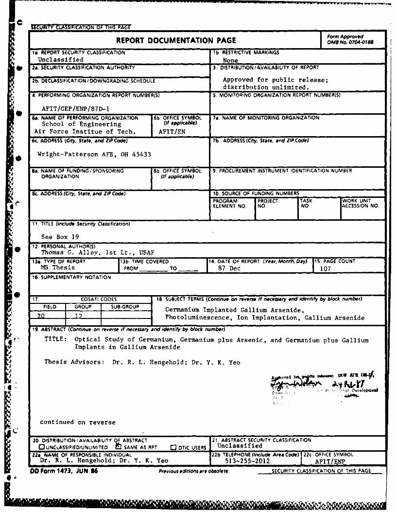
SECURITY CLASSIFICATION OF THIS PAGEForm Approved
REPORT DOCUMENTATION PAGE OM No. 070-018e
Is. REPORT SECURITY CLASSIFICATION lb. RESTRICTIVE MARKINGSUnclassified None
p 2a. SECURITY CLASSIFICATION AUTHORITY 3. DISTRIBUTION /AVAILABILITY OF REPORT
2b. DECLASSIFICATION/DOWNGRADING SCHEDULE Approved for public release;distribution unlimited.
4. PERFORMING ORGANIZATION REPORT NUMBER(S) 5. MONITOR NG ORGANIZATION REPORT NUMBER(S)
AFIT/GEP/ENP/87D-1
60. NAME OF PERFORMING ORGANIZATION 6b. OFFICE SYMBOL 7a. NAME OF MONITORING ORGANIZATIONSchool of Engineering (if applicable)
Air Force Institue of Tech. AFIT/EN
6c. ADDRESS (City, State, and ZIPCode) 7b. ADDRESS (City, State, and ZIP Code)
Wright-Patterson AFB, OH 45433
Ba. NAME OF FUNDING/SPONSORING 8b. OFFICE SYMBOL 9. PROCUREMENT INSTRUMENT IDENTIFICATION NUMBERORGANIZATION (If applicable)
ADDRESS (City, State, and ZIP Code) 10. SOURCE OF FUNDING NUMBERS
PROGRAM PROJECT TASK ' WORK UNITELEMENT NO. NO NO ACCESSION NO.
11. TITLE (Include Security Classification)
See Box 19
12. PERSONAL AUTHOR(S)Thomas G. Alley, 1st Lt., USAF
13e. TYPE OF REPORT 13b. TIME COVERED 14. DATE OF REPORT (Year, Month, Day) 1S. PAGE COUNTMS Thesis FROM TO 87 Dec 107
16. SUPPLEMENTARY NOTATION
17. COSATI CODES 18. SUBJECT TERMS (Continue on reverse if necessary and identify by block number)FIELD GROUP SUB-GROUP Germanium Implanted Gallium Arsenide,
12 Photoluminescence, Ion Implantation, Gallium Arsenide
19. ABSTRACT (Continue on reverse if necessary and identify by block number)TITLE: Optical Study of Germanium, Germanium plus Arsenic, and Germanium plus Gallium
Implants in Gallium Arsenide
Thesis Advisors: Dr. R. L. Hengehold; Dr. Y. K. Yeo
,Wo 1AW~U AM *-(
continued on reverse
20 DISTRIBUTION /AVAILABILITY OF ABSTRACT 21. ABSTRACT SECURITY CLASSIFICATIONEO UNCLASSIFIEDIUNLIMITED E3 SAME AS RPT D DTIC USERS Unclassified
22a NAME OF RESPONSIBLE INDIVIDUAL 22b TELEPHONE (Include Area Code) 22c OFFICE SYMBOLDr. R. L. Hengehold; Dr. Y. K. Yeo 513-255-2012 AFIT/ENP
DO Form 1473, JUN 86 Previous editions are obsolete. SECURITY CLASSIFICATION OF THIS PAGE*4 .
Block 19 cont.
The low temperature photoluminescence (PL) properties ofsingle implants of Ge and dual implants of Ge+As or Ge+Gainto semi-insulating Cr-doped GaAs have been analyzed. Roomtemperature implantation was performed at 120 keV. When dualimplantation was used, samples were implanted at the samedose and energy. Ion doses ranged from lxlO13 to lxlO1"/cm2 .Samples were encapsulated with SimN4 and then annealed attemperatures ranging from 700 to 9500C. SI2 N4 was removedprior to PL measurements.
A PL peak due to Ge-acceptors was identified. A boundexciton peak related to Ge-donors was also observed. Anacceptor peak due to residual Si was found in all samples.The heights of the Ge-acceptor peak and exciton peak werecompared to the height of the intrinsic Si-acceptor 4eak.
0 The height comparison was used in an effort to find trends ofGe-acceptor and Ge-donor transitions as a function of annealtemperature and Ion dese.
The PL data for GaAs:Ge+As showed a relative decrease ofthe Ge-acceptor related peak and an increase in the excitonpeak with increasing dose. This is generally consistent withelectrical measurements in previous work.
The PL data for GaAs:Ge at an anneal temperature of9500C also showed a relative decrease in the Ge-acceptorrelated peak and an increase in the exciton peak withincreasing dose. This is also consistent with electricaldata. However, trends of dose dependence at other annealtemperatures were more complicated.
The anneal temperature dependence of the Ge relatedpeaks for both GaAs:Ge and GaAs:Ge+As showed complicatedbehavior. At an anneal temperature of 800 0C, the Ge-acceptorrelated peak becomes obscured in a large Si-acceptor relatedpeak.
For GaAs:Ge+Ga, the addition of Ga to the implantationprocess generally enhances an observed Ga in As vacancyantisite defect transition.
iI~
S
*~~@* * S S *~ S 5 0 5 0 S *~ 0 0 0.